EP4160238A1 - Magnetic field detection device and magnetic field detection device array - Google Patents
Magnetic field detection device and magnetic field detection device array Download PDFInfo
- Publication number
- EP4160238A1 EP4160238A1 EP21811992.3A EP21811992A EP4160238A1 EP 4160238 A1 EP4160238 A1 EP 4160238A1 EP 21811992 A EP21811992 A EP 21811992A EP 4160238 A1 EP4160238 A1 EP 4160238A1
- Authority
- EP
- European Patent Office
- Prior art keywords
- magnetic field
- field detection
- cancel
- detection device
- magnetic
- Prior art date
- Legal status (The legal status is an assumption and is not a legal conclusion. Google has not performed a legal analysis and makes no representation as to the accuracy of the status listed.)
- Pending
Links
Images






Classifications
-
- G—PHYSICS
- G01—MEASURING; TESTING
- G01R—MEASURING ELECTRIC VARIABLES; MEASURING MAGNETIC VARIABLES
- G01R33/00—Arrangements or instruments for measuring magnetic variables
- G01R33/0094—Sensor arrays
-
- G—PHYSICS
- G01—MEASURING; TESTING
- G01R—MEASURING ELECTRIC VARIABLES; MEASURING MAGNETIC VARIABLES
- G01R33/00—Arrangements or instruments for measuring magnetic variables
- G01R33/0023—Electronic aspects, e.g. circuits for stimulation, evaluation, control; Treating the measured signals; calibration
- G01R33/0041—Electronic aspects, e.g. circuits for stimulation, evaluation, control; Treating the measured signals; calibration using feed-back or modulation techniques
-
- G—PHYSICS
- G01—MEASURING; TESTING
- G01R—MEASURING ELECTRIC VARIABLES; MEASURING MAGNETIC VARIABLES
- G01R33/00—Arrangements or instruments for measuring magnetic variables
- G01R33/02—Measuring direction or magnitude of magnetic fields or magnetic flux
- G01R33/025—Compensating stray fields
-
- G—PHYSICS
- G01—MEASURING; TESTING
- G01R—MEASURING ELECTRIC VARIABLES; MEASURING MAGNETIC VARIABLES
- G01R33/00—Arrangements or instruments for measuring magnetic variables
- G01R33/02—Measuring direction or magnitude of magnetic fields or magnetic flux
- G01R33/06—Measuring direction or magnitude of magnetic fields or magnetic flux using galvano-magnetic devices
- G01R33/09—Magnetoresistive devices
- G01R33/091—Constructional adaptation of the sensor to specific applications
-
- G—PHYSICS
- G01—MEASURING; TESTING
- G01R—MEASURING ELECTRIC VARIABLES; MEASURING MAGNETIC VARIABLES
- G01R33/00—Arrangements or instruments for measuring magnetic variables
- G01R33/02—Measuring direction or magnitude of magnetic fields or magnetic flux
- G01R33/0206—Three-component magnetometers
Definitions
- the present invention relates to a magnetic field detection device and, more particularly, to a magnetic field detection device capable of detecting a weak magnetic field without using a shield room.
- the present invention also relates to a magnetic field detection device array including a plurality of magnetic field detection devices.
- Patent Document 1 As a magnetic field detection device capable of detecting a weak magnetic field without a shield room, one described in Patent Document 1 is known.
- a magnetic field detection device exemplified in FIG. 1 of Patent Document 1 detects an environmental magnetic field using a reference magnetic sensor and makes a cancel current flow in a cancel coil based on the detected environmental magnetic field to thereby cancel the environmental magnetic field applied to a measurement magnetic sensor.
- a magnetic field detection device exemplified in FIG. 7 of Patent Document 1 extracts a environmental magnetic field component by adding output signals from a plurality of magnetic sensors and makes a cancel current flowing in cancel coils provided in the plurality of respective magnetic sensors to thereby cancel the environmental magnetic field applied to the plurality of magnetic sensors.
- a magnetic field detection device includes: a bobbin; a cancel coil wound around a winding core part of the bobbin; first and second magnetic sensors fixed to mutually different positions of the bobbin and configured to detect a magnetic field component in mutually the same direction; and a feedback circuit that makes a cancel current flow in the cancel coil according to an output signal of the first magnetic sensor to cancel an environmental magnetic field in a cancel space.
- the second magnetic sensor is disposed within the cancel space.
- the cancel coil is used in common for the first and second magnetic sensors, so that it is possible to reduce the number of components to be used and to simplify the circuit configuration.
- the first and second magnetic sensors may each be disposed at a position overlapping the inner diameter area of the cancel coil as viewed in the axial direction of the cancel coil. This makes it possible to reduce the overall size of the device.
- sensor heads of the first and second magnetic sensors may be different in position in the axial direction of the cancel coil. This makes it possible to prevent a signal magnetic field component from being cancelled by the cancel coil.
- the winding core part of the bobbin may have a first cavity opened at a first flange part and a second cavity opened at a second flange part, and the first and second magnetic sensors may be installed in the first and second cavities, respectively. This arrangement makes it possible to sufficiently separate the first and second magnetic sensors from each other.
- the sensor head of the first magnetic sensor may protrude from the first flange part of the bobbin, and the sensor head of the second magnetic sensor may protrude from the second flange part of the bobbin. This arrangement makes it possible to bring an object to be measured close to the second magnetic sensor.
- the magnetic field detection device may further have a circuit board fixed to the first or second flange part, and then the feedback circuit may be provided in the circuit board. This arrangement makes it possible to effectively use the first or second flange part.
- the magnetic field detection device may have a plurality of the second magnetic sensors. This arrangement makes it possible to measure the spatial distribution of the signal magnetic field component.
- the magnetic field detection device may further have a resistor connected in parallel to the cancel coil and having a resistance value larger than the equivalent series resistance of the cancel coil. This arrangement makes it possible to prevent oscillation of a feedback loop constituted by the first magnetic sensor, feedback circuit, and cancel coil.
- a magnetic field detection device array includes a plurality of the above-described magnetic field detection devices each having the plurality of second magnetic sensors.
- the plurality of magnetic field detection devices are arranged in a matrix with the axial directions of the cancel coils coinciding with one another.
- the present invention makes it possible to measure the spatial distribution of the signal magnetic field component over a wide range.
- a magnetic field detection device array is obtained by arranging a plurality of magnetic field detection devices in an array. At least one of the plurality of magnetic field detection devices has the same configuration as that of the magnetic field detection device having the plurality of second magnetic sensors.
- the remaining magnetic field detection devices each have a configuration obtained by removing the first magnetic sensor from the magnetic field detection device having the plurality of second magnetic sensors and configured to cancel the environmental magnetic field in a cancel space by making a cancel current flow in a cancel coil.
- the plurality of magnetic field detection devices constituting the magnetic field detection device array are arranged in a matrix with the axial directions of the cancel coils coinciding with one another.
- the present invention makes it possible to measure the spatial distribution of the signal magnetic field component over a wide range and also to reduce the number of magnetic sensors to be used.
- the plurality of second magnetic sensors provided in each of the plurality of magnetic field detection devices are disposed at each of the intersections between a plurality of first virtual lines extending in a first direction perpendicular to the axial direction of the cancel coil and a plurality of second virtual lines extending in a second direction perpendicular to the axial direction of the cancel coil and the first direction, and a pitch between the plurality of first virtual lines and a pitch between the plurality of second virtual lines may be equal to each other, whereby the spatial distribution of the signal magnetic field component in an xy plane as a detection surface can be measured at equal intervals.
- a magnetic field detection device and a magnetic field detection device array capable of detecting a weak magnetic field without using a shield room with a reduced number of components and a simplified circuit configuration.
- FIGS. 1 and 2 are views illustrating the outer appearance of a magnetic field detection device 1 according to a first embodiment of the present invention.
- FIG. 1 is a schematic perspective view seen from a measurement surface side
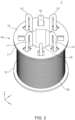
- FIG. 2 is a schematic perspective view seen from a back surface side.
- the magnetic field detection device 1 includes a bobbin 10 made of a resin material, a cancel coil C2 wound around the bobbin 10, and a plurality of magnetic sensors S1 and S21 to S24 fixed to the bobbin 10.
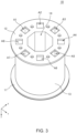
- the bobbin 10 includes a winding core part 13 and flange parts 11 and 12 provided at both ends of the winding core part 13 in the z-direction.
- the outer peripheral surface of the winding core part 13 has a circular shape as viewed in the z-direction.
- the cancel coil C2 is wound around the winding core part 13 of the bobbin 10, and thus the axial direction of the cancel coil C2 is the z-direction.
- the winding core part 13 is formed into a tubular shape and has a hollow part 14 extending in the z-direction.
- cavities A1 to A8 are formed in the winding core part 13 of the bobbin 10.
- the cavities A1 to A8 are through holes penetrating the winding core part 13 in the z-direction.
- One end of each of the cavities A1 to A8 in the z-direction is opened at the surface of the flange part 11, and the other end thereof in the z-direction is opened at the surface of the flange part 12.
- the radial direction positions of the respective cavities A1 to A8 are the same.
- the magnetic sensor S1 is installed in the cavity A6, and the magnetic sensors S21 to S24 are installed in the cavities A1, A3, A5, and A7 respectively.
- a sensor head of the magnetic sensor S1 protrudes in the z-direction from the flange part 11, and sensor heads of the respective magnetic sensors S21 to S24 protrude in the z-direction from the flange part 12.
- the magnetic sensors S1 and S21 to S24 are connected to a circuit board 15 fixed to the flange part 11 of the bobbin 10 through wirings L0 to L4, respectively.
- the cavities A2, A4, and A8 are vacant in the example illustrated in FIGS. 1 and 2 , other magnetic sensors may be installed in the cavities A2, A4, and A8. That is, at most eight magnetic sensors may be fixed to the bobbin 10.
- the magnetic sensors S1 and S21 to S24 are each disposed at a position overlapping the inner diameter area of the cancel coil C2 as viewed in the z-direction. Further, the position of the sensor head of the magnetic sensor S1 in the z-direction and the positions of the sensor heads of the respective magnetic sensors S21 to S24 in the z-direction differ from each other. The positions of the sensor heads of the respective magnetic sensors S21 to S24 in the z-direction are the same. Further, the radial direction positions of the sensor heads centering around the coil axis are the same among the magnetic sensors S1 and S21 to S24.
- the magnetic sensor S1 is a sensor for detecting an environmental magnetic field component such as terrestrial magnetism, while the magnetic sensors S21 to S24 are sensors for detecting a signal magnetic field component emitted from an object to be measured.
- the sensitivity axis directions of the magnetic sensors S1 and S21 to S24 are all along the z-direction. Although most part of each of the magnetic sensors S1 and S21 to S24 are positioned in the inner diameter area of the cancel coil C2, the sensor heads of the respective magnetic sensors S21 to S24 protrude from the flange part 12, as described above. This is intended to bring the sensor heads of the magnetic sensors S21 to S24 closer to an object to be measured.
- the sensor heads of the magnetic sensors S21 to S24 are embedded in the bobbin 10, a distance between an object to be measured and the sensor heads of the magnetic sensors S21 to S24 becomes large.
- the sensor head of the magnetic sensor S1 need not protrude from the flange part 11; however, to enhance the symmetry with the magnetic sensors S21 to S24, the magnetic sensor S1 preferably protrudes from the flange part 11 by the amount equal to the protruding amount of the magnetic sensors S21 to S24 from the flange part 12.
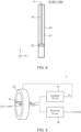
- FIG. 4 is a schematic view illustrating an example of the internal structure of the magnetic sensors S1 and S21 to S24.
- the magnetic sensors S1 and S21 to S24 have the same structure and each include a sensor housing body 20, a substrate 21 housed in the sensor housing body 20, a sensor chip 22, and a magnetism collector 23.
- the sensor chip 22 and magnetism collector 23 are mounted on the substrate 21.
- the magnetism collector 23 has a rod-like shape extending in the z-direction and is made of a high permeability material such as ferrite.
- One end of the magnetism collector 23 in the z-direction constitutes a sensor head H, and the sensor chip 22 is disposed at the other end of the magnetism collector 23 in the z-direction.
- FIG. 5 is a block diagram illustrating the circuit configuration of the magnetic field detection device 1 according to the present embodiment.
- the magnetic field detection device 1 includes a feedback circuit 31 connected to the magnetic sensor S1 and a detection circuit 32 connected to the magnetic sensors S21 to S24.
- the feedback circuit 31 is a circuit generating a feedback current F1 for canceling the environmental magnetic field component, and the feedback current F1 generated by the feedback circuit 31 is supplied to the cancel coil C2.
- the magnetic sensor S1, feedback circuit 31, and cancel coil C2 constitute a feedback loop for canceling the environmental magnetic field component.
- the detection circuit 32 generates, according to output signals from the magnetic sensors S21 to S24, a detection signal Vout indicating the signal magnetic field component emitted from an object to be measured.
- FIG. 6 is a schematic plan view of the sensor chip 22
- FIG. 7 is a schematic cross-sectional view taken along the line A-A in FIG. 6 .
- the sensor chip 22 has, on its element formation surface, four magnetoresistance effect elements M1 to M4 and a cancel coil C1.
- the cancel coil C1 is covered with an insulating film 24, and the magnetoresistance effect elements M1 to M4 are formed on the insulating film 24.
- the magnetoresistance effect elements M1 to M4 are covered with an insulating film 25.
- the magnetism collector 23 is disposed between the magnetoresistance effect elements M1, M2 and the magnetoresistance effect elements M3, M4 as viewed in the z-direction.
- a magnetic field in the z-direction collected by the magnetism collector 23 is distributed in the positive x-direction and the negative x-direction on the element formation surface of the sensor chip 22.
- magnetic field components in mutually opposite directions are applied to the magnetoresistance effect elements M1, M2 and magnetoresistance effect elements M3, M4.
- the fixed magnetization directions of the magnetoresistance effect elements M1 to M4 are made uniform in the positive x-direction or negative x-direction.
- the cancel coil C1 is disposed so as to overlap the magnetoresistance effect elements M1 to M4.
- cancel magnetic fields in mutually opposite directions are applied to the magnetoresistance effect elements M1, M2 and the magnetoresistance effect elements M3, M4.
- FIG. 8 is a circuit diagram of the feedback loop constituted by the magnetic sensor S1, feedback circuit 31, and cancel coil C2.
- the magnetoresistance effect elements M1 to M4 included in the magnetic sensor S1 are bridge-connected, and a differential signal generated thereby is supplied to a differential amplifier 31a included in the feedback circuit 31.
- the differential amplifier 31a generates the feedback current F1 based on the supplied differential signal.
- the feedback current F1 flows in the series-connected cancel coils C1 and C2. This causes the cancel coils C1 and C2 to generate a cancel magnetic field so as to make a differential signal component which is an output signal of the magnetic sensor S1 zero.
- a resistor R1 is connected in parallel to the cancel coil C2.
- the resistance value of the resistor R1 is larger than the equivalent series resistance (ESR) of the cancel coil C2 and is preferably set to 10 times or more, and more preferably, 100 times or more the ESR of the cancel coil C2.
- ESR equivalent series resistance
- FIG. 9 is a circuit diagram of a circuit constituted by the magnetic sensors S21 to S24 and detection circuit 32.
- the magnetoresistance effect elements M1 to M4 included in each of the magnetic sensors S21 to S24 are bridge-connected, and a differential signal generated thereby is supplied to a differential amplifier 32a.
- the differential amplifier 32a generates a feedback current F2 based on the differentia signal.
- the feedback current F2 flows in the cancel coil C1. This causes the cancel coil C1 to generate a cancel magnetic field so as to make a differential signal component as output signals of the magnetic sensors S21 to S24 zero.
- the detection circuit 32 has a resistor R2 that current-voltage converts the feedback current F2 and a voltage measurement circuit 33 that measures a voltage across the resistor R2.
- a detection signal Vout proportional to the amount of the flowing current is generated.
- FIG. 10 is a schematic view for explaining the positions of the magnetic sensors S1 and S21 to S24 in the radial direction.
- the magnetic sensor S1 is disposed at a position offset from the center of the inner diameter area of the cancel coil C2.
- the cancel coil C2 generates a cancel magnetic field so as to make the environmental magnetic field component to be applied to the magnetic sensor S1 zero.
- the environmental magnetic field component becomes zero not only at the position where the magnetic sensor S1 is disposed but also in a cancel space 40 distributed concentrically with the cancel coil C2. This is because that the intensity distribution of the cancel magnetic field spreads concentrically, so that when the environmental magnetic field component is uniform, it is completely cancelled in the area lying in the same radial position as the magnetic sensor S1.
- the cancel space 40 is present on the flange part 11 side where the sensor head of the magnetic sensor S1 is positioned, and also formed symmetrically on the flange part 12 side where the sensor heads of the magnetic sensors S21 to S24 are positioned.
- the magnetic sensors S21 to S24 are disposed in the cancel space 40 on the flange part 12 side.
- the environmental magnetic field component to be applied to the magnetic sensors S21 to S24 also becomes zero, with the result that only the signal magnetic field component emitted from an object to be measured is applied to the magnetic sensors S21 to S24.
- the cancel coil C2 is assigned in common to the five magnetic sensors S1 and S21 to S24, so that it is possible to reduce the number of components and to simplify the circuit configuration.
- the cavities A1 to A8 are disposed at the same radial position, so that the environmental magnetic field component to be applied to the magnetic sensors S21 to S24 becomes zero, no matter which one of the cavities any of the magnetic sensors S21 to S24 is installed in.
- the sensor head of the magnetic sensor S1 for detecting the environmental magnetic field component is provided on the flange part 11 side, and the sensor heads of the respective magnetic sensors S21 to S24 for detecting the signal magnetic field component are provided on the flange part 12 side, so that the signal magnetic field component emitted from an object to be measured is hardly applied to the magnetic sensor S1. This prevents a part or all of the signal magnetic field component from being cancelled.
- the signal magnetic field component emitted from the object to be measured can be detected in real time. Further, since the cancel coil C2 and magnetic sensors S1 and S21 to S24 are fixed to the same bobbin 10, displacement between the cancel coil C2 and the magnetic sensors S1 and S21 to S24 hardly occurs.
- the magnetic sensors S21 to S24 for detecting the signal magnetic field component can be arranged in a matrix in the xy plane.
- the magnetic sensor S21, S22, S23 or S24 is disposed at each of the intersections between the virtual lines x1 to x6 extending in the x-direction and the virtual lines y1 to y6 extending in the y-direction.
- the magnetic sensor S1 for detecting the environmental magnetic field component need not be provided in all the magnetic field detection devices 1, but it may be provided only in one of the magnetic field detection devices 1 and, in this case, the feedback current F1 may be supplied to the cancel coil C2 of each of the plurality of magnetic field detection devices 1. This can reduce the number of magnetic sensors to be used.
- FIG. 13 is a schematic cross-sectional view for explaining the structure of a magnetic field detection device 2 according to a second embodiment of the present invention.
- FIG. 14 is a schematically exploded perspective view of the outer appearance of the magnetic field detection device 2.
- the magnetic field detection device 2 according to the second embodiment differs from the magnetic field detection device 1 according to the first embodiment in that it includes a bobbin 50 inserted into the hollow part 14 of the bobbin 10 and a cancel coil C3 wound around a winding core part 53 of the bobbin 50.
- Other basic configurations are the same as those of the magnetic field detection device 1 according to the first embodiment, so the same reference numerals are given to the same elements, and overlapping description will be omitted.
- the bobbin 50 has the winding core part 53 and flange parts 51 and 52 provided at both ends of the winding core part 53 in the z-direction.
- the cancel coil C3 is wound around the winding core part 53 of the bobbin 50, and thus the axial direction of the cancel coil C3 is the z-direction.
- the cancel coil C3 is connected in series to the cancel coil C2. As a result, it is possible to generate a stronger cancel magnetic field than in the magnetic field detection device 1 according to the first embodiment.
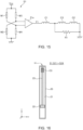
- the cancel coil C3 may be wound around the magnetism collector 23 in the magnetic sensor S1, as illustrated in FIG. 16 . With this configuration, even when the environmental magnetic field component is relatively strong, the magnetism collector 23 can be prevented from being magnetically saturated.
- the configuration illustrated in FIG. 16 is applicable to the magnetic sensors S21 to S24.
- FIGS. 17 to 19 are schematic perspective views illustrating the outer appearances of magnetic field detection devices 3 to 5 according to third to fifth embodiments of the present invention.
- the magnetic field detection device 3 according to the third embodiment differs from the magnetic field detection device 1 according to the first embodiment in that the bobbin 10 has a quadrangular shape as viewed in the z-direction.
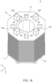
- the magnetic field detection device 4 according to the fourth embodiment differs from the magnetic field detection device 1 according to the first embodiment in that the bobbin 10 has an octagonal shape as viewed in the z-direction.
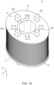
- the magnetic field detection device 5 according to the fifth embodiment differs from the magnetic field detection device 1 according to the first embodiment in that the bobbin 10 has an elliptic shape as viewed in the z-direction.
- the shape of the bobbin is not limited to a circular shape in the present invention.
- FIG. 20 is a schematic perspective view illustrating the outer appearance of a magnetic field detection device 6 according to a sixth embodiment of the present invention.
- the magnetic field detection device 6 according to the sixth embodiment differs from the magnetic field detection device 1 according to the first embodiment in that the position of the magnetic sensor S1 in the z-direction and the positions of the magnetic sensors S21 to S24 in the z-direction are the same and that the position of the magnetic sensor S1 in the radial direction centering around the coil axis and the positions of the magnetic sensors S21 to S24 in the radial direction centering around the coil axis are different.
- the magnetic sensor S1 is positioned at the center of the coil axis.
- the magnetic sensor S1 and the magnetic sensors S21 to S24 may be the same in position in the z-direction in the present invention. Further, in the present embodiment, the magnetic sensor S1 and the magnetic sensors S21 to S24 are different in position in the radial direction centering around the coil axis, so that when the environmental magnetic field component is completely cancelled at the position (center of the coil axis) where the magnetic sensor S1 is installed, it remains at the positions (positions offset from the center of the coil axis) where the magnetic sensors S21 to S24 are installed. Therefore, in the present embodiment, it is necessary to adjust the gain of the feedback loop so as not to completely cancel the environmental magnetic field component at the position of the magnetic sensor S1 but to completely cancel the environmental magnetic field component at the positions of the magnetic sensors S21 to S24.
- FIG. 21 is a schematic perspective view illustrating the outer appearance of a magnetic field detection device 7 according to a seventh embodiment of the present invention.
- the magnetic field detection device 7 according to the seventh embodiment differs from the magnetic field detection device 1 according to the first embodiment in that the areas of the respective flange parts 11 and 12 in the radial direction are enlarged and that cavities B1 to B8 are formed on a radially outer side of the winding core part 13.
- the four magnetic sensors S21 to S24 are installed respectively in any one of the cavities A1 to A8 positioned on a radially inner side, and the four magnetic sensors S1 are installed in the cavities B1 to B8 positioned on the radially outer side.
- all the cavities for installation of the magnetic sensors need not be the same in radial position, but a plurality of cavities different in radial position may be formed in the bobbin.
- the number of the magnetic sensors S1 for detecting the environmental magnetic field component is not limited to one, but may be two or more.
- the numbers of the magnetic sensors for detecting the signal magnetic field component is four, and the number of the magnetic sensors for detecting the environmental magnetic field component is one in the magnetic field detection device 1 according to the first embodiment, the numbers of the magnetic sensors for detecting the signa magnetic field component and environmental magnetic field component are not particularly limited to specific numbers.
Landscapes
- Physics & Mathematics (AREA)
- Condensed Matter Physics & Semiconductors (AREA)
- General Physics & Mathematics (AREA)
- Measuring Magnetic Variables (AREA)
- Shielding Devices Or Components To Electric Or Magnetic Fields (AREA)
Abstract
Description
- The present invention relates to a magnetic field detection device and, more particularly, to a magnetic field detection device capable of detecting a weak magnetic field without using a shield room. The present invention also relates to a magnetic field detection device array including a plurality of magnetic field detection devices.
- As a magnetic field detection device capable of detecting a weak magnetic field without a shield room, one described in
Patent Document 1 is known. A magnetic field detection device exemplified inFIG. 1 ofPatent Document 1 detects an environmental magnetic field using a reference magnetic sensor and makes a cancel current flow in a cancel coil based on the detected environmental magnetic field to thereby cancel the environmental magnetic field applied to a measurement magnetic sensor. On the other hand, a magnetic field detection device exemplified inFIG. 7 ofPatent Document 1 extracts a environmental magnetic field component by adding output signals from a plurality of magnetic sensors and makes a cancel current flowing in cancel coils provided in the plurality of respective magnetic sensors to thereby cancel the environmental magnetic field applied to the plurality of magnetic sensors. - [Patent Document 1]
JP 2017-133993A - However, in the magnetic field detection device exemplified in
FIG. 1 ofPatent Document 1, different cancel coils are assigned respectively to the measurement magnetic sensor and the reference magnetic sensor, so that the number of components is large. On the other hand, in the magnetic field detection device exemplified inFIG. 7 ofPatent Document 1, cancel coils are assigned to the plurality of respective magnetic sensors, thus also increasing the number of components. Further, in the magnetic field detection device exemplified inFIG. 7 ofPatent Document 1, it is necessary to add output signals from the plurality of magnetic sensors, thus complicating the circuit configuration. - It is therefore an object of the present invention to reduce the number of components and simplifying the circuit configuration in a magnetic field detection device and a magnetic field detection device array capable of detecting a weak magnetic field without using a shield room.
- A magnetic field detection device according to the present invention includes: a bobbin; a cancel coil wound around a winding core part of the bobbin; first and second magnetic sensors fixed to mutually different positions of the bobbin and configured to detect a magnetic field component in mutually the same direction; and a feedback circuit that makes a cancel current flow in the cancel coil according to an output signal of the first magnetic sensor to cancel an environmental magnetic field in a cancel space. The second magnetic sensor is disposed within the cancel space.
- According to the present invention, the cancel coil is used in common for the first and second magnetic sensors, so that it is possible to reduce the number of components to be used and to simplify the circuit configuration.
- In the present invention, the first and second magnetic sensors may each be disposed at a position overlapping the inner diameter area of the cancel coil as viewed in the axial direction of the cancel coil. This makes it possible to reduce the overall size of the device.
- In the present invention, sensor heads of the first and second magnetic sensors may be different in position in the axial direction of the cancel coil. This makes it possible to prevent a signal magnetic field component from being cancelled by the cancel coil. In this case, the winding core part of the bobbin may have a first cavity opened at a first flange part and a second cavity opened at a second flange part, and the first and second magnetic sensors may be installed in the first and second cavities, respectively. This arrangement makes it possible to sufficiently separate the first and second magnetic sensors from each other. Further, in this case, the sensor head of the first magnetic sensor may protrude from the first flange part of the bobbin, and the sensor head of the second magnetic sensor may protrude from the second flange part of the bobbin. This arrangement makes it possible to bring an object to be measured close to the second magnetic sensor.
- The magnetic field detection device according to the present invention may further have a circuit board fixed to the first or second flange part, and then the feedback circuit may be provided in the circuit board. This arrangement makes it possible to effectively use the first or second flange part.
- The magnetic field detection device according to the present invention may have a plurality of the second magnetic sensors. This arrangement makes it possible to measure the spatial distribution of the signal magnetic field component.
- The magnetic field detection device according to the present invention may further have a resistor connected in parallel to the cancel coil and having a resistance value larger than the equivalent series resistance of the cancel coil. This arrangement makes it possible to prevent oscillation of a feedback loop constituted by the first magnetic sensor, feedback circuit, and cancel coil.
- A magnetic field detection device array according to one aspect of the present invention includes a plurality of the above-described magnetic field detection devices each having the plurality of second magnetic sensors. The plurality of magnetic field detection devices are arranged in a matrix with the axial directions of the cancel coils coinciding with one another. The present invention makes it possible to measure the spatial distribution of the signal magnetic field component over a wide range.
- A magnetic field detection device array according to another aspect of the present invention is obtained by arranging a plurality of magnetic field detection devices in an array. At least one of the plurality of magnetic field detection devices has the same configuration as that of the magnetic field detection device having the plurality of second magnetic sensors. The remaining magnetic field detection devices each have a configuration obtained by removing the first magnetic sensor from the magnetic field detection device having the plurality of second magnetic sensors and configured to cancel the environmental magnetic field in a cancel space by making a cancel current flow in a cancel coil. The plurality of magnetic field detection devices constituting the magnetic field detection device array are arranged in a matrix with the axial directions of the cancel coils coinciding with one another. The present invention makes it possible to measure the spatial distribution of the signal magnetic field component over a wide range and also to reduce the number of magnetic sensors to be used.
- In the present invention, the plurality of second magnetic sensors provided in each of the plurality of magnetic field detection devices are disposed at each of the intersections between a plurality of first virtual lines extending in a first direction perpendicular to the axial direction of the cancel coil and a plurality of second virtual lines extending in a second direction perpendicular to the axial direction of the cancel coil and the first direction, and a pitch between the plurality of first virtual lines and a pitch between the plurality of second virtual lines may be equal to each other, whereby the spatial distribution of the signal magnetic field component in an xy plane as a detection surface can be measured at equal intervals.
- According to the present invention, there can be provided a magnetic field detection device and a magnetic field detection device array capable of detecting a weak magnetic field without using a shield room with a reduced number of components and a simplified circuit configuration.
-
-
FIG. 1 is a schematic perspective view illustrating a magneticfield detection device 1 according to a first embodiment of the present invention seen from a measurement surface side. -
FIG. 2 is a schematic perspective view illustrating the magneticfield detection device 1 seen from a back surface side. -
FIG. 3 is a schematic perspective view illustrating the outer appearance of abobbin 10. -
FIG. 4 is a schematic view illustrating an example of the internal structure of the magnetic sensors S1 and S21 to S24. -
FIG. 5 is a block diagram illustrating the circuit configuration of the magneticfield detection device 1. -
FIG. 6 is a schematic plan view of thesensor chip 22. -
FIG. 7 is a schematic cross-sectional view taken along the line A-A inFIG. 6 . -
FIG. 8 is a circuit diagram of the feedback loop constituted by the magnetic sensor S1,feedback circuit 31, and cancel coil C2. -
FIG. 9 is a circuit diagram of the magnetic sensors S21 to S24 anddetection circuit 32. -
FIG. 10 is a schematic view for explaining the positions of the magnetic sensors S1 and S21 to S24 in the radial direction. -
FIG. 11 is a schematic view for explaining the position of acancel space 40. -
FIG. 12 is a schematic view for explaining an example in which a plurality of the magneticfield detection devices 1 are arranged in an array. -
FIG. 13 is a schematic cross-sectional view for explaining the structure of a magneticfield detection device 2 according to a second embodiment of the present invention. -
FIG. 14 is a schematically exploded perspective view of the outer appearance of the magneticfield detection device 2. -
FIG. 15 is a circuit diagram of the feedback loop constituted by the magnetic sensor S1,feedback circuit 31, and cancel coils C2 and C3. -
FIG. 16 is a schematic view illustrating an example of the internal structure of the magnetic sensors S1 and S21 to S24 including the cancel coil C3. -
FIG. 17 is a schematic perspective view illustrating the outer appearances of magneticfield detection device 3 according to a third embodiment of the present invention. -
FIG. 18 is a schematic perspective view illustrating the outer appearances of magneticfield detection device 4 according to a fourth embodiment of the present invention. -
FIG. 19 is a schematic perspective view illustrating the outer appearances of magneticfield detection device 5 according to a fifth embodiment of the present invention. -
FIG. 20 is a schematic perspective view illustrating the outer appearances of magneticfield detection device 6 according to a sixth embodiment of the present invention. -
FIG. 21 is a schematic perspective view illustrating the outer appearances of magneticfield detection device 7 according to a seventh embodiment of the present invention. - Hereinafter, preferred embodiments of the present invention will be described in detail with reference to the accompanying drawings.
-
FIGS. 1 and2 are views illustrating the outer appearance of a magneticfield detection device 1 according to a first embodiment of the present invention.FIG. 1 is a schematic perspective view seen from a measurement surface side, andFIG. 2 is a schematic perspective view seen from a back surface side. - As illustrated in
FIGS. 1 and2 , the magneticfield detection device 1 according to the first embodiment includes abobbin 10 made of a resin material, a cancel coil C2 wound around thebobbin 10, and a plurality of magnetic sensors S1 and S21 to S24 fixed to thebobbin 10. As illustrated inFIG. 3 , thebobbin 10 includes a windingcore part 13 andflange parts core part 13 in the z-direction. The outer peripheral surface of the windingcore part 13 has a circular shape as viewed in the z-direction. The cancel coil C2 is wound around the windingcore part 13 of thebobbin 10, and thus the axial direction of the cancel coil C2 is the z-direction. The windingcore part 13 is formed into a tubular shape and has ahollow part 14 extending in the z-direction. - In the present embodiment, eight cavities A1 to A8 are formed in the winding
core part 13 of thebobbin 10. The cavities A1 to A8 are through holes penetrating the windingcore part 13 in the z-direction. One end of each of the cavities A1 to A8 in the z-direction is opened at the surface of theflange part 11, and the other end thereof in the z-direction is opened at the surface of theflange part 12. The radial direction positions of the respective cavities A1 to A8 are the same. In the present embodiment, the magnetic sensor S1 is installed in the cavity A6, and the magnetic sensors S21 to S24 are installed in the cavities A1, A3, A5, and A7 respectively. A sensor head of the magnetic sensor S1 protrudes in the z-direction from theflange part 11, and sensor heads of the respective magnetic sensors S21 to S24 protrude in the z-direction from theflange part 12. The magnetic sensors S1 and S21 to S24 are connected to acircuit board 15 fixed to theflange part 11 of thebobbin 10 through wirings L0 to L4, respectively. Although the cavities A2, A4, and A8 are vacant in the example illustrated inFIGS. 1 and2 , other magnetic sensors may be installed in the cavities A2, A4, and A8. That is, at most eight magnetic sensors may be fixed to thebobbin 10. - With the above configuration, the magnetic sensors S1 and S21 to S24 are each disposed at a position overlapping the inner diameter area of the cancel coil C2 as viewed in the z-direction. Further, the position of the sensor head of the magnetic sensor S1 in the z-direction and the positions of the sensor heads of the respective magnetic sensors S21 to S24 in the z-direction differ from each other. The positions of the sensor heads of the respective magnetic sensors S21 to S24 in the z-direction are the same. Further, the radial direction positions of the sensor heads centering around the coil axis are the same among the magnetic sensors S1 and S21 to S24.
- The magnetic sensor S1 is a sensor for detecting an environmental magnetic field component such as terrestrial magnetism, while the magnetic sensors S21 to S24 are sensors for detecting a signal magnetic field component emitted from an object to be measured. The sensitivity axis directions of the magnetic sensors S1 and S21 to S24 are all along the z-direction. Although most part of each of the magnetic sensors S1 and S21 to S24 are positioned in the inner diameter area of the cancel coil C2, the sensor heads of the respective magnetic sensors S21 to S24 protrude from the
flange part 12, as described above. This is intended to bring the sensor heads of the magnetic sensors S21 to S24 closer to an object to be measured. That is, when the sensor heads of the magnetic sensors S21 to S24 are embedded in thebobbin 10, a distance between an object to be measured and the sensor heads of the magnetic sensors S21 to S24 becomes large. On the other hand, the sensor head of the magnetic sensor S1 need not protrude from theflange part 11; however, to enhance the symmetry with the magnetic sensors S21 to S24, the magnetic sensor S1 preferably protrudes from theflange part 11 by the amount equal to the protruding amount of the magnetic sensors S21 to S24 from theflange part 12. -
FIG. 4 is a schematic view illustrating an example of the internal structure of the magnetic sensors S1 and S21 to S24. - In the example illustrated in
FIG. 4 , the magnetic sensors S1 and S21 to S24 have the same structure and each include asensor housing body 20, asubstrate 21 housed in thesensor housing body 20, asensor chip 22, and amagnetism collector 23. Thesensor chip 22 andmagnetism collector 23 are mounted on thesubstrate 21. Themagnetism collector 23 has a rod-like shape extending in the z-direction and is made of a high permeability material such as ferrite. One end of themagnetism collector 23 in the z-direction constitutes a sensor head H, and thesensor chip 22 is disposed at the other end of themagnetism collector 23 in the z-direction. With this configuration, the signal magnetic field component in the z-direction component emitted from an object to be measured positioned in the vicinity of the sensor head H is collected by themagnetism collector 23 to be applied to thesensor chip 22. -
FIG. 5 is a block diagram illustrating the circuit configuration of the magneticfield detection device 1 according to the present embodiment. - As illustrated in
FIG. 5 , the magneticfield detection device 1 according to the present embodiment includes afeedback circuit 31 connected to the magnetic sensor S1 and adetection circuit 32 connected to the magnetic sensors S21 to S24. Thefeedback circuit 31 is a circuit generating a feedback current F1 for canceling the environmental magnetic field component, and the feedback current F1 generated by thefeedback circuit 31 is supplied to the cancel coil C2. As a result, the magnetic sensor S1,feedback circuit 31, and cancel coil C2 constitute a feedback loop for canceling the environmental magnetic field component. On the other hand, thedetection circuit 32 generates, according to output signals from the magnetic sensors S21 to S24, a detection signal Vout indicating the signal magnetic field component emitted from an object to be measured. -
FIG. 6 is a schematic plan view of thesensor chip 22, andFIG. 7 is a schematic cross-sectional view taken along the line A-A inFIG. 6 . - As illustrated in
FIGS. 6 and 7 , thesensor chip 22 has, on its element formation surface, four magnetoresistance effect elements M1 to M4 and a cancel coil C1. The cancel coil C1 is covered with an insulatingfilm 24, and the magnetoresistance effect elements M1 to M4 are formed on the insulatingfilm 24. The magnetoresistance effect elements M1 to M4 are covered with an insulatingfilm 25. Themagnetism collector 23 is disposed between the magnetoresistance effect elements M1, M2 and the magnetoresistance effect elements M3, M4 as viewed in the z-direction. With this configuration, a magnetic field in the z-direction collected by themagnetism collector 23 is distributed in the positive x-direction and the negative x-direction on the element formation surface of thesensor chip 22. As a result, magnetic field components in mutually opposite directions are applied to the magnetoresistance effect elements M1, M2 and magnetoresistance effect elements M3, M4. The fixed magnetization directions of the magnetoresistance effect elements M1 to M4 are made uniform in the positive x-direction or negative x-direction. - The cancel coil C1 is disposed so as to overlap the magnetoresistance effect elements M1 to M4. When a cancel current is made to flow in the cancel coil C1, cancel magnetic fields in mutually opposite directions are applied to the magnetoresistance effect elements M1, M2 and the magnetoresistance effect elements M3, M4.
-
FIG. 8 is a circuit diagram of the feedback loop constituted by the magnetic sensor S1,feedback circuit 31, and cancel coil C2. - As illustrated in
FIG. 8 , the magnetoresistance effect elements M1 to M4 included in the magnetic sensor S1 are bridge-connected, and a differential signal generated thereby is supplied to adifferential amplifier 31a included in thefeedback circuit 31. Thedifferential amplifier 31a generates the feedback current F1 based on the supplied differential signal. The feedback current F1 flows in the series-connected cancel coils C1 and C2. This causes the cancel coils C1 and C2 to generate a cancel magnetic field so as to make a differential signal component which is an output signal of the magnetic sensor S1 zero. - In the present embodiment, a resistor R1 is connected in parallel to the cancel coil C2. The resistance value of the resistor R1 is larger than the equivalent series resistance (ESR) of the cancel coil C2 and is preferably set to 10 times or more, and more preferably, 100 times or more the ESR of the cancel coil C2. Thus, of the feedback current F1, a lower frequency component attributable to terrestrial magnetism flows in the cancel coil C2, while a high frequency component that is a cause of oscillation is detoured to the resistor R1. This makes it possible to properly cancel the environmental magnetic field component such as terrestrial magnetism while preventing oscillation of the feedback loop.
-
FIG. 9 is a circuit diagram of a circuit constituted by the magnetic sensors S21 to S24 anddetection circuit 32. - As illustrated in
FIG. 9 , the magnetoresistance effect elements M1 to M4 included in each of the magnetic sensors S21 to S24 are bridge-connected, and a differential signal generated thereby is supplied to adifferential amplifier 32a. Thedifferential amplifier 32a generates a feedback current F2 based on the differentia signal. The feedback current F2 flows in the cancel coil C1. This causes the cancel coil C1 to generate a cancel magnetic field so as to make a differential signal component as output signals of the magnetic sensors S21 to S24 zero. - Further, the
detection circuit 32 has a resistor R2 that current-voltage converts the feedback current F2 and avoltage measurement circuit 33 that measures a voltage across the resistor R2. Thus, when the feedback current F2 flows, a detection signal Vout proportional to the amount of the flowing current is generated. -
FIG. 10 is a schematic view for explaining the positions of the magnetic sensors S1 and S21 to S24 in the radial direction. - As illustrated in
FIG. 10 , as viewed in the axial direction (z-direction) of the cancel coil C2, the magnetic sensor S1 is disposed at a position offset from the center of the inner diameter area of the cancel coil C2. As described above, the cancel coil C2 generates a cancel magnetic field so as to make the environmental magnetic field component to be applied to the magnetic sensor S1 zero. However, the environmental magnetic field component becomes zero not only at the position where the magnetic sensor S1 is disposed but also in a cancelspace 40 distributed concentrically with the cancel coil C2. This is because that the intensity distribution of the cancel magnetic field spreads concentrically, so that when the environmental magnetic field component is uniform, it is completely cancelled in the area lying in the same radial position as the magnetic sensor S1. - As illustrated in
FIG. 11 , the cancelspace 40 is present on theflange part 11 side where the sensor head of the magnetic sensor S1 is positioned, and also formed symmetrically on theflange part 12 side where the sensor heads of the magnetic sensors S21 to S24 are positioned. In the present embodiment, the magnetic sensors S21 to S24 are disposed in the cancelspace 40 on theflange part 12 side. Thus, the environmental magnetic field component to be applied to the magnetic sensors S21 to S24 also becomes zero, with the result that only the signal magnetic field component emitted from an object to be measured is applied to the magnetic sensors S21 to S24. This makes it possible to detect even a weak magnetic field without using a shield room. In addition, the cancel coil C2 is assigned in common to the five magnetic sensors S1 and S21 to S24, so that it is possible to reduce the number of components and to simplify the circuit configuration. - In the present embodiment, the cavities A1 to A8 are disposed at the same radial position, so that the environmental magnetic field component to be applied to the magnetic sensors S21 to S24 becomes zero, no matter which one of the cavities any of the magnetic sensors S21 to S24 is installed in. In addition, in the present embodiment, the sensor head of the magnetic sensor S1 for detecting the environmental magnetic field component is provided on the
flange part 11 side, and the sensor heads of the respective magnetic sensors S21 to S24 for detecting the signal magnetic field component are provided on theflange part 12 side, so that the signal magnetic field component emitted from an object to be measured is hardly applied to the magnetic sensor S1. This prevents a part or all of the signal magnetic field component from being cancelled. Thus, when measurement is performed with an object to be measured that generates a weak magnetic field brought close to the sensor heads of the magnetic sensors S21 to S24, the signal magnetic field component emitted from the object to be measured can be detected in real time. Further, since the cancel coil C2 and magnetic sensors S1 and S21 to S24 are fixed to thesame bobbin 10, displacement between the cancel coil C2 and the magnetic sensors S1 and S21 to S24 hardly occurs. - As descried above, using the magnetic
field detection device 1 according to the present embodiment allows a weak magnetic field to be detected with high sensitivity by a simple configuration. Further, as illustrated inFIG. 12 , when a plurality of the magneticfield detection devices 1 according to the present embodiment are arranged in an array with the axial directions of the cancel coils coinciding with one another, the magnetic sensors S21 to S24 for detecting the signal magnetic field component can be arranged in a matrix in the xy plane. In the example illustrated inFIG. 12 , the magnetic sensor S21, S22, S23 or S24 is disposed at each of the intersections between the virtual lines x1 to x6 extending in the x-direction and the virtual lines y1 to y6 extending in the y-direction. By designing a pitch P between the virtual lines x1 to x6 and a pitch P between the virtual lines y1 to y6 equal to each other, the spatial distribution of the signal magnetic field component can be measured over a wide range. - When a plurality of the magnetic
field detection devices 1 are arranged in an array, the magnetic sensor S1 for detecting the environmental magnetic field component need not be provided in all the magneticfield detection devices 1, but it may be provided only in one of the magneticfield detection devices 1 and, in this case, the feedback current F1 may be supplied to the cancel coil C2 of each of the plurality of magneticfield detection devices 1. This can reduce the number of magnetic sensors to be used. -
FIG. 13 is a schematic cross-sectional view for explaining the structure of a magneticfield detection device 2 according to a second embodiment of the present invention.FIG. 14 is a schematically exploded perspective view of the outer appearance of the magneticfield detection device 2. - As illustrated in
FIG. 13 , the magneticfield detection device 2 according to the second embodiment differs from the magneticfield detection device 1 according to the first embodiment in that it includes abobbin 50 inserted into thehollow part 14 of thebobbin 10 and a cancel coil C3 wound around a windingcore part 53 of thebobbin 50. Other basic configurations are the same as those of the magneticfield detection device 1 according to the first embodiment, so the same reference numerals are given to the same elements, and overlapping description will be omitted. - The
bobbin 50 has the windingcore part 53 andflange parts core part 53 in the z-direction. The cancel coil C3 is wound around the windingcore part 53 of thebobbin 50, and thus the axial direction of the cancel coil C3 is the z-direction. As illustrated inFIG. 15 , the cancel coil C3 is connected in series to the cancel coil C2. As a result, it is possible to generate a stronger cancel magnetic field than in the magneticfield detection device 1 according to the first embodiment. - The cancel coil C3 may be wound around the
magnetism collector 23 in the magnetic sensor S1, as illustrated inFIG. 16 . With this configuration, even when the environmental magnetic field component is relatively strong, themagnetism collector 23 can be prevented from being magnetically saturated. The configuration illustrated inFIG. 16 is applicable to the magnetic sensors S21 to S24. -
FIGS. 17 to 19 are schematic perspective views illustrating the outer appearances of magneticfield detection devices 3 to 5 according to third to fifth embodiments of the present invention. - As illustrated in
FIG. 17 , the magneticfield detection device 3 according to the third embodiment differs from the magneticfield detection device 1 according to the first embodiment in that thebobbin 10 has a quadrangular shape as viewed in the z-direction. As illustrated inFIG. 18 , the magneticfield detection device 4 according to the fourth embodiment differs from the magneticfield detection device 1 according to the first embodiment in that thebobbin 10 has an octagonal shape as viewed in the z-direction. As illustrated inFIG. 19 , the magneticfield detection device 5 according to the fifth embodiment differs from the magneticfield detection device 1 according to the first embodiment in that thebobbin 10 has an elliptic shape as viewed in the z-direction. - As exemplified by the magnetic
field detection devices 3 to 5 according to the third to fifth embodiments, the shape of the bobbin is not limited to a circular shape in the present invention. -
FIG. 20 is a schematic perspective view illustrating the outer appearance of a magneticfield detection device 6 according to a sixth embodiment of the present invention. - As illustrated in
FIG. 20 , the magneticfield detection device 6 according to the sixth embodiment differs from the magneticfield detection device 1 according to the first embodiment in that the position of the magnetic sensor S1 in the z-direction and the positions of the magnetic sensors S21 to S24 in the z-direction are the same and that the position of the magnetic sensor S1 in the radial direction centering around the coil axis and the positions of the magnetic sensors S21 to S24 in the radial direction centering around the coil axis are different. In the example illustrated inFIG. 20 , the magnetic sensor S1 is positioned at the center of the coil axis. - As exemplified by the magnetic
field detection device 6 according to the sixth embodiment, the magnetic sensor S1 and the magnetic sensors S21 to S24 may be the same in position in the z-direction in the present invention. Further, in the present embodiment, the magnetic sensor S1 and the magnetic sensors S21 to S24 are different in position in the radial direction centering around the coil axis, so that when the environmental magnetic field component is completely cancelled at the position (center of the coil axis) where the magnetic sensor S1 is installed, it remains at the positions (positions offset from the center of the coil axis) where the magnetic sensors S21 to S24 are installed. Therefore, in the present embodiment, it is necessary to adjust the gain of the feedback loop so as not to completely cancel the environmental magnetic field component at the position of the magnetic sensor S1 but to completely cancel the environmental magnetic field component at the positions of the magnetic sensors S21 to S24. -
FIG. 21 is a schematic perspective view illustrating the outer appearance of a magneticfield detection device 7 according to a seventh embodiment of the present invention. - As illustrated in
FIG. 21 , the magneticfield detection device 7 according to the seventh embodiment differs from the magneticfield detection device 1 according to the first embodiment in that the areas of therespective flange parts core part 13. In the example illustrated inFIG. 21 , the four magnetic sensors S21 to S24 are installed respectively in any one of the cavities A1 to A8 positioned on a radially inner side, and the four magnetic sensors S1 are installed in the cavities B1 to B8 positioned on the radially outer side. - As exemplified by the magnetic
field detection device 7 according to the seventh embodiment, all the cavities for installation of the magnetic sensors need not be the same in radial position, but a plurality of cavities different in radial position may be formed in the bobbin. Further, the number of the magnetic sensors S1 for detecting the environmental magnetic field component is not limited to one, but may be two or more. - While the preferred embodiment of the present invention has been described, the present invention is not limited to the above embodiment, and various modifications may be made within the scope of the present invention, and all such modifications are included in the present invention.
- For example, although the number of the magnetic sensors for detecting the signal magnetic field component is four, and the number of the magnetic sensors for detecting the environmental magnetic field component is one in the magnetic
field detection device 1 according to the first embodiment, the numbers of the magnetic sensors for detecting the signa magnetic field component and environmental magnetic field component are not particularly limited to specific numbers. -
- 1-7
- magnetic field detection device
- 10, 50
- bobbin
- 11, 12, 51, 52
- flange part
- 13, 53
- winding core part
- 14
- hollow part
- 15
- circuit board
- 20
- sensor housing body
- 21
- substrate
- 22
- sensor chip
- 23
- magnetism collector
- 24, 25
- insulating film
- 31
- feedback circuit
- 31a
- differential amplifier
- 32
- detection circuit
- 32a
- differential amplifier
- 33
- voltage measurement circuit
- 40
- cancel space
- A1-A8, B1-B8
- cavity
- C1-C3
- cancel coil
- F1, F2
- feedback current
- H
- sensor head
- L0-L4
- wiring
- M1-M4
- magnetoresistance effect element
- R1, R2
- resistor
- S1, S21-S24
- magnetic sensor
Claims (11)
- A magnetic field detection device comprising:a bobbin;a cancel coil wound around a winding core part of the bobbin;first and second magnetic sensors fixed to mutually different positions of the bobbin and configured to detect a magnetic field component in mutually a same direction; anda feedback circuit that makes a cancel current flow in the cancel coil according to an output signal of the first magnetic sensor to cancel an environmental magnetic field in a cancel space,wherein the second magnetic sensor is disposed within the cancel space.
- The magnetic field detection device as claimed in claim 1, wherein each of the first and second magnetic sensors is disposed at a position overlapping an inner diameter area of the cancel coil as viewed in an axial direction of the cancel coil.
- The magnetic field detection device as claimed in claim 1 or 2, wherein sensor heads of the first and second magnetic sensors are different in position in an axial direction of the cancel coil.
- The magnetic field detection device as claimed in claim 3,wherein the winding core part of the bobbin has a first cavity opened at a first flange part and a second cavity opened at a second flange part,wherein the first magnetic sensor is installed in the first cavity, andwherein the second magnetic sensor is installed in the second cavity.
- The magnetic field detection device as claimed in claim 4,wherein the sensor head of the first magnetic sensor protrudes from the first flange part of the bobbin, andwherein the sensor head of the second magnetic sensor protrudes from the second flange part of the bobbin.
- The magnetic field detection device as claimed in claim 4 or 5, further comprising a circuit board fixed to the first or second flange part,
wherein the feedback circuit is provided in the circuit board. - The magnetic field detection device as claimed in any one of claims 1 to 6, wherein a plurality of the second magnetic sensors are provided.
- The magnetic field detection device as claimed in any one of claims 1 to 7, further comprising a resistor connected in parallel to the cancel coil and having a resistance value larger than an equivalent series resistance of the cancel coil.
- A magnetic field detection device array comprising a plurality of the magnetic field detection devices as claimed in claim 7,
wherein the plurality of magnetic field detection devices are arranged in a matrix with axial directions of the cancel coils coinciding with one another. - A magnetic field detection device array obtained by arranging a plurality of magnetic field detection devices in an array,wherein at least one of the plurality of magnetic field detection devices has a same configuration as that of the magnetic field detection device as claimed in claim 7,wherein remaining magnetic field detection devices each have a configuration obtained by removing the first magnetic sensor from the magnetic field detection device as claimed in claim 7 and configured to cancel the environmental magnetic field in a cancel space by making the cancel current flow in the cancel coil, andwherein the plurality of magnetic field detection devices are arranged in a matrix with axial directions of the cancel coils coinciding with one another.
- The magnetic field detection device array as claimed in claim 9 or 10,wherein the plurality of second magnetic sensors provided in each of the plurality of magnetic field detection devices are disposed at each of the intersections between a plurality of first virtual lines extending in a first direction perpendicular to the axial direction of the cancel coil and a plurality of second virtual lines extending in a second direction perpendicular to the axial direction of the cancel coil and the first direction, andwherein a pitch between the plurality of first virtual lines and a pitch between the plurality of second virtual lines are equal to each other.
Applications Claiming Priority (2)
| Application Number | Priority Date | Filing Date | Title |
|---|---|---|---|
| JP2020092889A JP7521933B2 (en) | 2020-05-28 | 2020-05-28 | Magnetic field detection device and magnetic field detection device array |
| PCT/JP2021/017622 WO2021241174A1 (en) | 2020-05-28 | 2021-05-10 | Magnetic field detection device and magnetic field detection device array |
Publications (2)
| Publication Number | Publication Date |
|---|---|
| EP4160238A1 true EP4160238A1 (en) | 2023-04-05 |
| EP4160238A4 EP4160238A4 (en) | 2024-06-26 |
Family
ID=78723375
Family Applications (1)
| Application Number | Title | Priority Date | Filing Date |
|---|---|---|---|
| EP21811992.3A Pending EP4160238A4 (en) | 2020-05-28 | 2021-05-10 | MAGNETIC FIELD DETECTION DEVICE AND MAGNETIC FIELD DETECTION DEVICE ARRAY |
Country Status (5)
| Country | Link |
|---|---|
| US (1) | US12117506B2 (en) |
| EP (1) | EP4160238A4 (en) |
| JP (1) | JP7521933B2 (en) |
| CN (1) | CN115667966B (en) |
| WO (1) | WO2021241174A1 (en) |
Families Citing this family (4)
| Publication number | Priority date | Publication date | Assignee | Title |
|---|---|---|---|---|
| EP4427250A1 (en) | 2021-11-04 | 2024-09-11 | Safefields Technologies Ltd. | System and method for active cancellation of magnetic fields |
| IL291200B1 (en) * | 2022-03-08 | 2026-02-01 | סייפפילדס טכנול& | Magnetic field cancellation system |
| CN118244371B (en) * | 2024-05-24 | 2024-09-27 | 微传智能科技(常州)有限公司 | Geomagnetic detection magnetic circuit structure with magnetic attraction |
| CN120977718B (en) * | 2025-10-22 | 2026-01-30 | 杭州极弱磁场国家重大科技基础设施研究院 | Self-adaptive active-adjustment type demagnetizing circuit and device of magnetic shielding device |
Family Cites Families (17)
| Publication number | Priority date | Publication date | Assignee | Title |
|---|---|---|---|---|
| JP4016750B2 (en) * | 2002-07-15 | 2007-12-05 | 富士電機ホールディングス株式会社 | Magnetic detector |
| JP4263544B2 (en) * | 2003-06-23 | 2009-05-13 | 株式会社日立ハイテクノロジーズ | Magnetic field measuring device |
| JP2005351746A (en) * | 2004-06-10 | 2005-12-22 | Sumitomo Denko Hightecs Kk | Signal detecting apparatus |
| JP4919873B2 (en) * | 2007-05-10 | 2012-04-18 | 株式会社竹中工務店 | Magnetic shield device |
| EP2851702A1 (en) * | 2013-09-11 | 2015-03-25 | Seiko Epson Corporation | Magnetic shielding apparatus and magnetic shielding method |
| DE102015009603B4 (en) | 2015-07-24 | 2019-05-09 | Te Connectivity Germany Gmbh | DEVICE FOR MEASURING AN ELECTRIC CURRENT THROUGH A CIRCUIT |
| US11073576B2 (en) * | 2015-11-04 | 2021-07-27 | Tdk Corporation | Magnetic field detection device and magnetic field detection method |
| JP6666732B2 (en) | 2016-01-29 | 2020-03-18 | 株式会社アドバンテスト | Magnetic noise canceling device and magnetic field measuring device |
| JP6724459B2 (en) * | 2016-03-23 | 2020-07-15 | Tdk株式会社 | Magnetic sensor |
| JP6969142B2 (en) | 2017-04-12 | 2021-11-24 | Tdk株式会社 | Magnetic sensor |
| JP6890484B2 (en) * | 2017-07-03 | 2021-06-18 | 株式会社日立ハイテク | Magnetic field measuring device and measured magnetic field display method |
| JP6968720B2 (en) * | 2018-01-31 | 2021-11-17 | ヒロセ電機株式会社 | Wire winding method and magnetic sensor |
| CN108459076A (en) | 2018-06-22 | 2018-08-28 | 河北布鲁克科技有限公司 | A kind of magnetic shielding system for wire rope flaw detection |
| JP6658823B2 (en) * | 2018-08-24 | 2020-03-04 | Tdk株式会社 | Magnetic sensor and magnetic sensor system |
| JP7115224B2 (en) * | 2018-11-02 | 2022-08-09 | Tdk株式会社 | magnetic sensor |
| JP6791237B2 (en) * | 2018-12-28 | 2020-11-25 | Tdk株式会社 | Magnetic sensor device |
| JP7525297B2 (en) * | 2020-05-08 | 2024-07-30 | 旭化成エレクトロニクス株式会社 | Magnetic field measurement device, magnetic field measurement method, and magnetic field measurement program |
-
2020
- 2020-05-28 JP JP2020092889A patent/JP7521933B2/en active Active
-
2021
- 2021-05-10 US US17/927,134 patent/US12117506B2/en active Active
- 2021-05-10 EP EP21811992.3A patent/EP4160238A4/en active Pending
- 2021-05-10 CN CN202180038524.8A patent/CN115667966B/en active Active
- 2021-05-10 WO PCT/JP2021/017622 patent/WO2021241174A1/en not_active Ceased
Also Published As
| Publication number | Publication date |
|---|---|
| WO2021241174A1 (en) | 2021-12-02 |
| US20230204686A1 (en) | 2023-06-29 |
| CN115667966A (en) | 2023-01-31 |
| JP2021188976A (en) | 2021-12-13 |
| JP7521933B2 (en) | 2024-07-24 |
| US12117506B2 (en) | 2024-10-15 |
| EP4160238A4 (en) | 2024-06-26 |
| CN115667966B (en) | 2026-03-27 |
Similar Documents
| Publication | Publication Date | Title |
|---|---|---|
| US12117506B2 (en) | Magnetic field detection device and magnetic field detection device array | |
| US12066506B2 (en) | Magnetic sensor | |
| EP2682763B1 (en) | Magnetic transducer and current transducer for measuring an electrical current | |
| EP2520945B1 (en) | Magnetic field detecting apparatus and current sensor | |
| US8836317B2 (en) | Current sensor | |
| US20120146620A1 (en) | Current sensor | |
| JP2020071198A (en) | Magnetic sensor | |
| US12188997B2 (en) | Magnetic field detection device and magnetic field detection device array | |
| JP6974898B2 (en) | Current converter | |
| US20250116735A1 (en) | Magnetic sensor | |
| JP7479888B2 (en) | Magnetic Field Detection Device | |
| US11573280B2 (en) | Coil assembly for compensation current sensor | |
| US20250048554A1 (en) | Flexible printed circuit rogowski coil | |
| JPH022544B2 (en) | ||
| WO2025033425A1 (en) | Current sensor, measuring device, and measuring method | |
| WO2025033424A1 (en) | Current sensor, measurement device, and measurement method | |
| CN120595203A (en) | Magnetic measurement device | |
| US20040263156A1 (en) | Magnetoresistive angle sensor | |
| JP2025026376A (en) | Current Sensors and Measuring Devices | |
| JP2615961B2 (en) | Current detection unit | |
| JPH02163666A (en) | Magnetic detection unit | |
| JPH0754333B2 (en) | Current detection unit | |
| JPH0754331B2 (en) | Current detection unit |
Legal Events
| Date | Code | Title | Description |
|---|---|---|---|
| STAA | Information on the status of an ep patent application or granted ep patent |
Free format text: STATUS: THE INTERNATIONAL PUBLICATION HAS BEEN MADE |
|
| PUAI | Public reference made under article 153(3) epc to a published international application that has entered the european phase |
Free format text: ORIGINAL CODE: 0009012 |
|
| STAA | Information on the status of an ep patent application or granted ep patent |
Free format text: STATUS: REQUEST FOR EXAMINATION WAS MADE |
|
| 17P | Request for examination filed |
Effective date: 20221205 |
|
| AK | Designated contracting states |
Kind code of ref document: A1 Designated state(s): AL AT BE BG CH CY CZ DE DK EE ES FI FR GB GR HR HU IE IS IT LI LT LU LV MC MK MT NL NO PL PT RO RS SE SI SK SM TR |
|
| DAV | Request for validation of the european patent (deleted) | ||
| DAX | Request for extension of the european patent (deleted) | ||
| REG | Reference to a national code |
Ref country code: DE Ref legal event code: R079 Free format text: PREVIOUS MAIN CLASS: G01R0033020000 Ipc: G01R0033025000 |
|
| A4 | Supplementary search report drawn up and despatched |
Effective date: 20240524 |
|
| RIC1 | Information provided on ipc code assigned before grant |
Ipc: H05K 9/00 20060101ALI20240517BHEP Ipc: G01R 33/02 20060101ALI20240517BHEP Ipc: G01R 33/00 20060101ALI20240517BHEP Ipc: G01R 33/025 20060101AFI20240517BHEP |