EP4156891A1 - Capacitor with an electrically conductive layer coupled with a metal layer of the capacitor - Google Patents
Capacitor with an electrically conductive layer coupled with a metal layer of the capacitor Download PDFInfo
- Publication number
- EP4156891A1 EP4156891A1 EP22197335.7A EP22197335A EP4156891A1 EP 4156891 A1 EP4156891 A1 EP 4156891A1 EP 22197335 A EP22197335 A EP 22197335A EP 4156891 A1 EP4156891 A1 EP 4156891A1
- Authority
- EP
- European Patent Office
- Prior art keywords
- metal layer
- layer
- capacitor
- electrically conductive
- conductive layer
- Prior art date
- Legal status (The legal status is an assumption and is not a legal conclusion. Google has not performed a legal analysis and makes no representation as to the accuracy of the status listed.)
- Pending
Links
- 229910052751 metal Inorganic materials 0.000 title claims abstract description 172
- 239000002184 metal Substances 0.000 title claims abstract description 172
- 239000003990 capacitor Substances 0.000 title claims abstract description 57
- 238000000034 method Methods 0.000 claims abstract description 40
- -1 BaHfO3 Inorganic materials 0.000 claims description 14
- BASFCYQUMIYNBI-UHFFFAOYSA-N platinum Chemical compound [Pt] BASFCYQUMIYNBI-UHFFFAOYSA-N 0.000 claims description 14
- QVGXLLKOCUKJST-UHFFFAOYSA-N atomic oxygen Chemical compound [O] QVGXLLKOCUKJST-UHFFFAOYSA-N 0.000 claims description 13
- 229910052760 oxygen Inorganic materials 0.000 claims description 13
- 239000001301 oxygen Substances 0.000 claims description 13
- 229910052782 aluminium Inorganic materials 0.000 claims description 9
- XAGFODPZIPBFFR-UHFFFAOYSA-N aluminium Chemical compound [Al] XAGFODPZIPBFFR-UHFFFAOYSA-N 0.000 claims description 9
- QCWXUUIWCKQGHC-UHFFFAOYSA-N Zirconium Chemical compound [Zr] QCWXUUIWCKQGHC-UHFFFAOYSA-N 0.000 claims description 8
- 229910052735 hafnium Inorganic materials 0.000 claims description 8
- VBJZVLUMGGDVMO-UHFFFAOYSA-N hafnium atom Chemical compound [Hf] VBJZVLUMGGDVMO-UHFFFAOYSA-N 0.000 claims description 8
- 229910052726 zirconium Inorganic materials 0.000 claims description 8
- KJTLSVCANCCWHF-UHFFFAOYSA-N Ruthenium Chemical compound [Ru] KJTLSVCANCCWHF-UHFFFAOYSA-N 0.000 claims description 7
- 229910052788 barium Inorganic materials 0.000 claims description 7
- DSAJWYNOEDNPEQ-UHFFFAOYSA-N barium atom Chemical compound [Ba] DSAJWYNOEDNPEQ-UHFFFAOYSA-N 0.000 claims description 7
- 229910017052 cobalt Inorganic materials 0.000 claims description 7
- 239000010941 cobalt Substances 0.000 claims description 7
- GUTLYIVDDKVIGB-UHFFFAOYSA-N cobalt atom Chemical compound [Co] GUTLYIVDDKVIGB-UHFFFAOYSA-N 0.000 claims description 7
- 229910052746 lanthanum Inorganic materials 0.000 claims description 7
- FZLIPJUXYLNCLC-UHFFFAOYSA-N lanthanum atom Chemical compound [La] FZLIPJUXYLNCLC-UHFFFAOYSA-N 0.000 claims description 7
- 229910052697 platinum Inorganic materials 0.000 claims description 7
- 229910052707 ruthenium Inorganic materials 0.000 claims description 7
- 229910052712 strontium Inorganic materials 0.000 claims description 7
- CIOAGBVUUVVLOB-UHFFFAOYSA-N strontium atom Chemical compound [Sr] CIOAGBVUUVVLOB-UHFFFAOYSA-N 0.000 claims description 7
- 229910002254 LaCoO3 Inorganic materials 0.000 claims description 6
- ZOKXTWBITQBERF-UHFFFAOYSA-N Molybdenum Chemical compound [Mo] ZOKXTWBITQBERF-UHFFFAOYSA-N 0.000 claims description 6
- 229910004410 SrSnO3 Inorganic materials 0.000 claims description 6
- 229910002370 SrTiO3 Inorganic materials 0.000 claims description 6
- ATJFFYVFTNAWJD-UHFFFAOYSA-N Tin Chemical compound [Sn] ATJFFYVFTNAWJD-UHFFFAOYSA-N 0.000 claims description 6
- 229910002113 barium titanate Inorganic materials 0.000 claims description 6
- 229910021523 barium zirconate Inorganic materials 0.000 claims description 6
- 229910052750 molybdenum Inorganic materials 0.000 claims description 6
- 239000011733 molybdenum Substances 0.000 claims description 6
- 229910052702 rhenium Inorganic materials 0.000 claims description 6
- WUAPFZMCVAUBPE-UHFFFAOYSA-N rhenium atom Chemical compound [Re] WUAPFZMCVAUBPE-UHFFFAOYSA-N 0.000 claims description 6
- 229910052703 rhodium Inorganic materials 0.000 claims description 6
- 239000010948 rhodium Substances 0.000 claims description 6
- MHOVAHRLVXNVSD-UHFFFAOYSA-N rhodium atom Chemical compound [Rh] MHOVAHRLVXNVSD-UHFFFAOYSA-N 0.000 claims description 6
- 229910052718 tin Inorganic materials 0.000 claims description 6
- WFKWXMTUELFFGS-UHFFFAOYSA-N tungsten Chemical compound [W] WFKWXMTUELFFGS-UHFFFAOYSA-N 0.000 claims description 6
- 229910052721 tungsten Inorganic materials 0.000 claims description 6
- 239000010937 tungsten Substances 0.000 claims description 6
- 239000000463 material Substances 0.000 abstract description 19
- 230000008569 process Effects 0.000 abstract description 19
- 230000000694 effects Effects 0.000 abstract description 7
- 239000010410 layer Substances 0.000 description 217
- 239000000758 substrate Substances 0.000 description 31
- 238000010586 diagram Methods 0.000 description 17
- 238000004891 communication Methods 0.000 description 15
- 239000012212 insulator Substances 0.000 description 14
- VYPSYNLAJGMNEJ-UHFFFAOYSA-N Silicium dioxide Chemical compound O=[Si]=O VYPSYNLAJGMNEJ-UHFFFAOYSA-N 0.000 description 10
- 239000004065 semiconductor Substances 0.000 description 8
- XUIMIQQOPSSXEZ-UHFFFAOYSA-N Silicon Chemical compound [Si] XUIMIQQOPSSXEZ-UHFFFAOYSA-N 0.000 description 6
- 239000003989 dielectric material Substances 0.000 description 6
- 229910052710 silicon Inorganic materials 0.000 description 6
- 239000010703 silicon Substances 0.000 description 6
- 125000006850 spacer group Chemical group 0.000 description 5
- 238000004519 manufacturing process Methods 0.000 description 4
- 150000002739 metals Chemical class 0.000 description 4
- 235000012239 silicon dioxide Nutrition 0.000 description 4
- 239000000377 silicon dioxide Substances 0.000 description 4
- 229910052581 Si3N4 Inorganic materials 0.000 description 3
- 239000002019 doping agent Substances 0.000 description 3
- 229910052732 germanium Inorganic materials 0.000 description 3
- GNPVGFCGXDBREM-UHFFFAOYSA-N germanium atom Chemical compound [Ge] GNPVGFCGXDBREM-UHFFFAOYSA-N 0.000 description 3
- 239000011521 glass Substances 0.000 description 3
- HQVNEWCFYHHQES-UHFFFAOYSA-N silicon nitride Chemical compound N12[Si]34N5[Si]62N3[Si]51N64 HQVNEWCFYHHQES-UHFFFAOYSA-N 0.000 description 3
- BTOCFTAWZMMTNB-UHFFFAOYSA-N 1,2,3,4,5-pentachloro-6-(4-chlorophenyl)benzene Chemical compound C1=CC(Cl)=CC=C1C1=C(Cl)C(Cl)=C(Cl)C(Cl)=C1Cl BTOCFTAWZMMTNB-UHFFFAOYSA-N 0.000 description 2
- ZOXJGFHDIHLPTG-UHFFFAOYSA-N Boron Chemical compound [B] ZOXJGFHDIHLPTG-UHFFFAOYSA-N 0.000 description 2
- OKTJSMMVPCPJKN-UHFFFAOYSA-N Carbon Chemical compound [C] OKTJSMMVPCPJKN-UHFFFAOYSA-N 0.000 description 2
- PXHVJJICTQNCMI-UHFFFAOYSA-N Nickel Chemical compound [Ni] PXHVJJICTQNCMI-UHFFFAOYSA-N 0.000 description 2
- KDLHZDBZIXYQEI-UHFFFAOYSA-N Palladium Chemical compound [Pd] KDLHZDBZIXYQEI-UHFFFAOYSA-N 0.000 description 2
- 229910000676 Si alloy Inorganic materials 0.000 description 2
- RTAQQCXQSZGOHL-UHFFFAOYSA-N Titanium Chemical compound [Ti] RTAQQCXQSZGOHL-UHFFFAOYSA-N 0.000 description 2
- 229910045601 alloy Inorganic materials 0.000 description 2
- 239000000956 alloy Substances 0.000 description 2
- 238000000137 annealing Methods 0.000 description 2
- 229910052785 arsenic Inorganic materials 0.000 description 2
- RQNWIZPPADIBDY-UHFFFAOYSA-N arsenic atom Chemical compound [As] RQNWIZPPADIBDY-UHFFFAOYSA-N 0.000 description 2
- 238000000429 assembly Methods 0.000 description 2
- 230000000712 assembly Effects 0.000 description 2
- 238000000231 atomic layer deposition Methods 0.000 description 2
- 230000015572 biosynthetic process Effects 0.000 description 2
- 229910052796 boron Inorganic materials 0.000 description 2
- 229910052799 carbon Inorganic materials 0.000 description 2
- 230000008878 coupling Effects 0.000 description 2
- 238000010168 coupling process Methods 0.000 description 2
- 238000005859 coupling reaction Methods 0.000 description 2
- 238000005137 deposition process Methods 0.000 description 2
- 239000003822 epoxy resin Substances 0.000 description 2
- 238000005530 etching Methods 0.000 description 2
- BHEPBYXIRTUNPN-UHFFFAOYSA-N hydridophosphorus(.) (triplet) Chemical compound [PH] BHEPBYXIRTUNPN-UHFFFAOYSA-N 0.000 description 2
- MRELNEQAGSRDBK-UHFFFAOYSA-N lanthanum(3+);oxygen(2-) Chemical compound [O-2].[O-2].[O-2].[La+3].[La+3] MRELNEQAGSRDBK-UHFFFAOYSA-N 0.000 description 2
- 238000012986 modification Methods 0.000 description 2
- 230000004048 modification Effects 0.000 description 2
- 229920000647 polyepoxide Polymers 0.000 description 2
- HBMJWWWQQXIZIP-UHFFFAOYSA-N silicon carbide Chemical compound [Si+]#[C-] HBMJWWWQQXIZIP-UHFFFAOYSA-N 0.000 description 2
- 229910010271 silicon carbide Inorganic materials 0.000 description 2
- 229910052814 silicon oxide Inorganic materials 0.000 description 2
- 229910052715 tantalum Inorganic materials 0.000 description 2
- GUVRBAGPIYLISA-UHFFFAOYSA-N tantalum atom Chemical compound [Ta] GUVRBAGPIYLISA-UHFFFAOYSA-N 0.000 description 2
- 229910052719 titanium Inorganic materials 0.000 description 2
- 239000010936 titanium Substances 0.000 description 2
- JBRZTFJDHDCESZ-UHFFFAOYSA-N AsGa Chemical compound [As]#[Ga] JBRZTFJDHDCESZ-UHFFFAOYSA-N 0.000 description 1
- RYGMFSIKBFXOCR-UHFFFAOYSA-N Copper Chemical compound [Cu] RYGMFSIKBFXOCR-UHFFFAOYSA-N 0.000 description 1
- 229910001218 Gallium arsenide Inorganic materials 0.000 description 1
- 229910000530 Gallium indium arsenide Inorganic materials 0.000 description 1
- 229910000673 Indium arsenide Inorganic materials 0.000 description 1
- GPXJNWSHGFTCBW-UHFFFAOYSA-N Indium phosphide Chemical compound [In]#P GPXJNWSHGFTCBW-UHFFFAOYSA-N 0.000 description 1
- 239000004642 Polyimide Substances 0.000 description 1
- 229910000577 Silicon-germanium Inorganic materials 0.000 description 1
- GWEVSGVZZGPLCZ-UHFFFAOYSA-N Titan oxide Chemical compound O=[Ti]=O GWEVSGVZZGPLCZ-UHFFFAOYSA-N 0.000 description 1
- HCHKCACWOHOZIP-UHFFFAOYSA-N Zinc Chemical compound [Zn] HCHKCACWOHOZIP-UHFFFAOYSA-N 0.000 description 1
- 229910026551 ZrC Inorganic materials 0.000 description 1
- OTCHGXYCWNXDOA-UHFFFAOYSA-N [C].[Zr] Chemical compound [C].[Zr] OTCHGXYCWNXDOA-UHFFFAOYSA-N 0.000 description 1
- KXNLCSXBJCPWGL-UHFFFAOYSA-N [Ga].[As].[In] Chemical compound [Ga].[As].[In] KXNLCSXBJCPWGL-UHFFFAOYSA-N 0.000 description 1
- XWCMFHPRATWWFO-UHFFFAOYSA-N [O-2].[Ta+5].[Sc+3].[O-2].[O-2].[O-2] Chemical compound [O-2].[Ta+5].[Sc+3].[O-2].[O-2].[O-2] XWCMFHPRATWWFO-UHFFFAOYSA-N 0.000 description 1
- LEVVHYCKPQWKOP-UHFFFAOYSA-N [Si].[Ge] Chemical compound [Si].[Ge] LEVVHYCKPQWKOP-UHFFFAOYSA-N 0.000 description 1
- ILCYGSITMBHYNK-UHFFFAOYSA-N [Si]=O.[Hf] Chemical compound [Si]=O.[Hf] ILCYGSITMBHYNK-UHFFFAOYSA-N 0.000 description 1
- CAVCGVPGBKGDTG-UHFFFAOYSA-N alumanylidynemethyl(alumanylidynemethylalumanylidenemethylidene)alumane Chemical compound [Al]#C[Al]=C=[Al]C#[Al] CAVCGVPGBKGDTG-UHFFFAOYSA-N 0.000 description 1
- 229910052787 antimony Inorganic materials 0.000 description 1
- WATWJIUSRGPENY-UHFFFAOYSA-N antimony atom Chemical compound [Sb] WATWJIUSRGPENY-UHFFFAOYSA-N 0.000 description 1
- 238000003491 array Methods 0.000 description 1
- VKJLWXGJGDEGSO-UHFFFAOYSA-N barium(2+);oxygen(2-);titanium(4+) Chemical compound [O-2].[O-2].[O-2].[Ti+4].[Ba+2] VKJLWXGJGDEGSO-UHFFFAOYSA-N 0.000 description 1
- 230000008901 benefit Effects 0.000 description 1
- 229910010293 ceramic material Inorganic materials 0.000 description 1
- 230000000052 comparative effect Effects 0.000 description 1
- 229910052802 copper Inorganic materials 0.000 description 1
- 239000010949 copper Substances 0.000 description 1
- 230000003247 decreasing effect Effects 0.000 description 1
- 230000000593 degrading effect Effects 0.000 description 1
- 230000003111 delayed effect Effects 0.000 description 1
- 230000001419 dependent effect Effects 0.000 description 1
- 238000000151 deposition Methods 0.000 description 1
- 230000008021 deposition Effects 0.000 description 1
- 238000009792 diffusion process Methods 0.000 description 1
- KPUWHANPEXNPJT-UHFFFAOYSA-N disiloxane Chemical class [SiH3]O[SiH3] KPUWHANPEXNPJT-UHFFFAOYSA-N 0.000 description 1
- 230000005670 electromagnetic radiation Effects 0.000 description 1
- 230000005669 field effect Effects 0.000 description 1
- 229940104869 fluorosilicate Drugs 0.000 description 1
- VTGARNNDLOTBET-UHFFFAOYSA-N gallium antimonide Chemical compound [Sb]#[Ga] VTGARNNDLOTBET-UHFFFAOYSA-N 0.000 description 1
- 229910000449 hafnium oxide Inorganic materials 0.000 description 1
- WIHZLLGSGQNAGK-UHFFFAOYSA-N hafnium(4+);oxygen(2-) Chemical compound [O-2].[O-2].[Hf+4] WIHZLLGSGQNAGK-UHFFFAOYSA-N 0.000 description 1
- WHJFNYXPKGDKBB-UHFFFAOYSA-N hafnium;methane Chemical compound C.[Hf] WHJFNYXPKGDKBB-UHFFFAOYSA-N 0.000 description 1
- 238000002513 implantation Methods 0.000 description 1
- 238000011065 in-situ storage Methods 0.000 description 1
- WPYVAWXEWQSOGY-UHFFFAOYSA-N indium antimonide Chemical compound [Sb]#[In] WPYVAWXEWQSOGY-UHFFFAOYSA-N 0.000 description 1
- RPQDHPTXJYYUPQ-UHFFFAOYSA-N indium arsenide Chemical compound [In]#[As] RPQDHPTXJYYUPQ-UHFFFAOYSA-N 0.000 description 1
- 239000011229 interlayer Substances 0.000 description 1
- 238000005468 ion implantation Methods 0.000 description 1
- 229910052741 iridium Inorganic materials 0.000 description 1
- GKOZUEZYRPOHIO-UHFFFAOYSA-N iridium atom Chemical compound [Ir] GKOZUEZYRPOHIO-UHFFFAOYSA-N 0.000 description 1
- JQJCSZOEVBFDKO-UHFFFAOYSA-N lead zinc Chemical compound [Zn].[Pb] JQJCSZOEVBFDKO-UHFFFAOYSA-N 0.000 description 1
- 230000007774 longterm Effects 0.000 description 1
- 238000007726 management method Methods 0.000 description 1
- 150000001247 metal acetylides Chemical class 0.000 description 1
- 229910001092 metal group alloy Inorganic materials 0.000 description 1
- 229910044991 metal oxide Inorganic materials 0.000 description 1
- 150000004706 metal oxides Chemical class 0.000 description 1
- NFFIWVVINABMKP-UHFFFAOYSA-N methylidynetantalum Chemical compound [Ta]#C NFFIWVVINABMKP-UHFFFAOYSA-N 0.000 description 1
- 239000002074 nanoribbon Substances 0.000 description 1
- 239000002070 nanowire Substances 0.000 description 1
- 229910052759 nickel Inorganic materials 0.000 description 1
- 229910052758 niobium Inorganic materials 0.000 description 1
- 239000010955 niobium Substances 0.000 description 1
- GUCVJGMIXFAOAE-UHFFFAOYSA-N niobium atom Chemical compound [Nb] GUCVJGMIXFAOAE-UHFFFAOYSA-N 0.000 description 1
- BCCOBQSFUDVTJQ-UHFFFAOYSA-N octafluorocyclobutane Chemical compound FC1(F)C(F)(F)C(F)(F)C1(F)F BCCOBQSFUDVTJQ-UHFFFAOYSA-N 0.000 description 1
- 235000019407 octafluorocyclobutane Nutrition 0.000 description 1
- 229920000620 organic polymer Polymers 0.000 description 1
- TWNQGVIAIRXVLR-UHFFFAOYSA-N oxo(oxoalumanyloxy)alumane Chemical compound O=[Al]O[Al]=O TWNQGVIAIRXVLR-UHFFFAOYSA-N 0.000 description 1
- KJXBRHIPHIVJCS-UHFFFAOYSA-N oxo(oxoalumanyloxy)lanthanum Chemical compound O=[Al]O[La]=O KJXBRHIPHIVJCS-UHFFFAOYSA-N 0.000 description 1
- SIWVEOZUMHYXCS-UHFFFAOYSA-N oxo(oxoyttriooxy)yttrium Chemical compound O=[Y]O[Y]=O SIWVEOZUMHYXCS-UHFFFAOYSA-N 0.000 description 1
- BPUBBGLMJRNUCC-UHFFFAOYSA-N oxygen(2-);tantalum(5+) Chemical compound [O-2].[O-2].[O-2].[O-2].[O-2].[Ta+5].[Ta+5] BPUBBGLMJRNUCC-UHFFFAOYSA-N 0.000 description 1
- RVTZCBVAJQQJTK-UHFFFAOYSA-N oxygen(2-);zirconium(4+) Chemical compound [O-2].[O-2].[Zr+4] RVTZCBVAJQQJTK-UHFFFAOYSA-N 0.000 description 1
- 238000004806 packaging method and process Methods 0.000 description 1
- 229910052763 palladium Inorganic materials 0.000 description 1
- 229920001721 polyimide Polymers 0.000 description 1
- 239000002861 polymer material Substances 0.000 description 1
- 229920001343 polytetrafluoroethylene Polymers 0.000 description 1
- 239000004810 polytetrafluoroethylene Substances 0.000 description 1
- 239000011148 porous material Substances 0.000 description 1
- 229910001925 ruthenium oxide Inorganic materials 0.000 description 1
- WOCIAKWEIIZHES-UHFFFAOYSA-N ruthenium(iv) oxide Chemical compound O=[Ru]=O WOCIAKWEIIZHES-UHFFFAOYSA-N 0.000 description 1
- 229910052706 scandium Inorganic materials 0.000 description 1
- SIXSYDAISGFNSX-UHFFFAOYSA-N scandium atom Chemical compound [Sc] SIXSYDAISGFNSX-UHFFFAOYSA-N 0.000 description 1
- 239000007787 solid Substances 0.000 description 1
- 238000003860 storage Methods 0.000 description 1
- VEALVRVVWBQVSL-UHFFFAOYSA-N strontium titanate Chemical compound [Sr+2].[O-][Ti]([O-])=O VEALVRVVWBQVSL-UHFFFAOYSA-N 0.000 description 1
- CZXRMHUWVGPWRM-UHFFFAOYSA-N strontium;barium(2+);oxygen(2-);titanium(4+) Chemical compound [O-2].[O-2].[O-2].[O-2].[Ti+4].[Sr+2].[Ba+2] CZXRMHUWVGPWRM-UHFFFAOYSA-N 0.000 description 1
- 229910003468 tantalcarbide Inorganic materials 0.000 description 1
- 229910001936 tantalum oxide Inorganic materials 0.000 description 1
- OCGWQDWYSQAFTO-UHFFFAOYSA-N tellanylidenelead Chemical compound [Pb]=[Te] OCGWQDWYSQAFTO-UHFFFAOYSA-N 0.000 description 1
- OGIDPMRJRNCKJF-UHFFFAOYSA-N titanium oxide Inorganic materials [Ti]=O OGIDPMRJRNCKJF-UHFFFAOYSA-N 0.000 description 1
- MTPVUVINMAGMJL-UHFFFAOYSA-N trimethyl(1,1,2,2,2-pentafluoroethyl)silane Chemical compound C[Si](C)(C)C(F)(F)C(F)(F)F MTPVUVINMAGMJL-UHFFFAOYSA-N 0.000 description 1
- 229910052727 yttrium Inorganic materials 0.000 description 1
- VWQVUPCCIRVNHF-UHFFFAOYSA-N yttrium atom Chemical compound [Y] VWQVUPCCIRVNHF-UHFFFAOYSA-N 0.000 description 1
- 229910052725 zinc Inorganic materials 0.000 description 1
- 239000011701 zinc Substances 0.000 description 1
- 229910001928 zirconium oxide Inorganic materials 0.000 description 1
- GFQYVLUOOAAOGM-UHFFFAOYSA-N zirconium(iv) silicate Chemical compound [Zr+4].[O-][Si]([O-])([O-])[O-] GFQYVLUOOAAOGM-UHFFFAOYSA-N 0.000 description 1
Images


Classifications
-
- H—ELECTRICITY
- H01—ELECTRIC ELEMENTS
- H01G—CAPACITORS; CAPACITORS, RECTIFIERS, DETECTORS, SWITCHING DEVICES OR LIGHT-SENSITIVE DEVICES, OF THE ELECTROLYTIC TYPE
- H01G4/00—Fixed capacitors; Processes of their manufacture
- H01G4/30—Stacked capacitors
-
- H—ELECTRICITY
- H01—ELECTRIC ELEMENTS
- H01G—CAPACITORS; CAPACITORS, RECTIFIERS, DETECTORS, SWITCHING DEVICES OR LIGHT-SENSITIVE DEVICES, OF THE ELECTROLYTIC TYPE
- H01G4/00—Fixed capacitors; Processes of their manufacture
- H01G4/002—Details
- H01G4/018—Dielectrics
- H01G4/06—Solid dielectrics
- H01G4/08—Inorganic dielectrics
-
- H—ELECTRICITY
- H01—ELECTRIC ELEMENTS
- H01G—CAPACITORS; CAPACITORS, RECTIFIERS, DETECTORS, SWITCHING DEVICES OR LIGHT-SENSITIVE DEVICES, OF THE ELECTROLYTIC TYPE
- H01G4/00—Fixed capacitors; Processes of their manufacture
- H01G4/35—Feed-through capacitors or anti-noise capacitors
-
- H—ELECTRICITY
- H01—ELECTRIC ELEMENTS
- H01L—SEMICONDUCTOR DEVICES NOT COVERED BY CLASS H10
- H01L28/00—Passive two-terminal components without a potential-jump or surface barrier for integrated circuits; Details thereof; Multistep manufacturing processes therefor
- H01L28/40—Capacitors
- H01L28/55—Capacitors with a dielectric comprising a perovskite structure material
-
- H—ELECTRICITY
- H01—ELECTRIC ELEMENTS
- H01L—SEMICONDUCTOR DEVICES NOT COVERED BY CLASS H10
- H01L28/00—Passive two-terminal components without a potential-jump or surface barrier for integrated circuits; Details thereof; Multistep manufacturing processes therefor
- H01L28/40—Capacitors
- H01L28/60—Electrodes
- H01L28/82—Electrodes with an enlarged surface, e.g. formed by texturisation
- H01L28/90—Electrodes with an enlarged surface, e.g. formed by texturisation having vertical extensions
Definitions
- Embodiments of the present disclosure generally relate to the field of semiconductor packaging, and in particular to capacitors within dies or packages.
- Embodiments described herein may be related to apparatuses, processes, and techniques directed to MIM capacitors that have a multiple trench structure to increase a charge density, where a dielectric of the MIM capacitor includes a perovskite-based high-k (dielectric constant) material.
- a first conductive layer such as a conductive metal
- a second conductive layer may be coupled with a bottom metal layer of the MIM.
- the first conductive layer may be electrically coupled with the top metal layer
- the second conductive layer may be electrically coupled with the bottom metal layer.
- the first conductive layer may extend the length of the top metal layer
- the second conductive layer may extend the length of the bottom metal layer.
- the top metal layer may be referred to as a first metal layer and a top electrode
- the bottom metal layer may be referred to as a second metal layer or a bottom electrode.
- a multiple trench structure may be used to increase the overall surface area of the active portion of the MIM capacitor. This may be done by narrowing the distances between the trenches, which may be referred to as increasing the density of the trenches, and/or increasing the height of the trenches. This increases the surface area to which the top metal layer, dielectric, and bottom metal layer are applied. However, by narrowing the distances between the trenches, during operation a resistor-capacitor (RC) effect on the MIM will be larger.
- RC resistor-capacitor
- the RC effect may be reduced by 100 times or more.
- phrase “A and/or B” means (A), (B), or (A and B).
- phrase “A, B, and/or C” means (A), (B), (C), (A and B), (A and C), (B and C), or (A, B and C).
- Coupled may mean one or more of the following. “Coupled” may mean that two or more elements are in direct physical or electrical contact. However, “coupled” may also mean that two or more elements indirectly contact each other, but yet still cooperate or interact with each other, and may mean that one or more other elements are coupled or connected between the elements that are said to be coupled with each other.
- directly coupled may mean that two or more elements are in direct contact.
- module may refer to, be part of, or include an ASIC, an electronic circuit, a processor (shared, dedicated, or group) and/or memory (shared, dedicated, or group) that execute one or more software or firmware programs, a combinational logic circuit, and/or other suitable components that provide the described functionality.
- FIG. 1 may depict one or more layers of one or more package assemblies.
- the layers depicted herein are depicted as examples of relative positions of the layers of the different package assemblies.
- the layers are depicted for the purposes of explanation, and are not drawn to scale. Therefore, comparative sizes of layers should not be assumed from the Figures, and sizes, thicknesses, or dimensions may be assumed for some embodiments only where specifically indicated or discussed.
- Various embodiments may include any suitable combination of the above-described embodiments including alternative (or) embodiments of embodiments that are described in conjunctive form (and) above (e.g., the "and” may be “and/or”).
- some embodiments may include one or more articles of manufacture (e.g., non-transitory computer-readable media) having instructions, stored thereon, that when executed result in actions of any of the above-described embodiments.
- some embodiments may include apparatuses or systems having any suitable means for carrying out the various operations of the above-described embodiments.
- FIGs. 1A-1B illustrate a schematic and a block diagram that shows metal-insulator-metal (MIM) capacitors within a die and a package.
- FIG. 1A illustrates a block diagram that shows MIM capacitors from regulator to die.
- FIG. 1B illustrates a schematic that shows MIM capacitors within a die and a package.
- diagram 100 is a schematic that shows a portion of various circuitry associated with the components of the system 160.
- die 162 may be electrically coupled with package 164 using interconnect 163.
- the package 164 may be electrically coupled with a printed circuit board (PCB) 166 using interconnect 165.
- PCB 166 may be a motherboard.
- a voltage regulator 177 (not shown in FIG. 1B ) may be used to provide power to the die 162, the package 164, and/or the PCB 166.
- a capacitor 170 which in embodiments may be a MIM capacitor, may be included on the die 162.
- another capacitor 172 which in embodiments may be a MIM capacitor, may also be included on the package 164.
- the capacitors 170, 172 may be multiple capacitors that provide a higher capacitance density that may minimize a first droop during load switching, as shown with respect to highlighted area 174 of graph 180.
- graph 180 shows a relationship between voltage and time (in microseconds), with respect to various voltage droops.
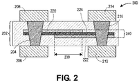
- FIG. 2 illustrates a block diagram of a cross-section of a two plate MIM capacitor using perovskite-based high-k materials, in accordance with various embodiments.
- MIM 200 includes a first metal layer 220 and a second metal layer 222 that are separated by dielectric 224.
- dielectric 224 may be a perovskite-based high-k dielectric.
- the first metal layer 220, the layers of dielectric 224, and the second metal layer 222 may be referred to as a MIM stack.
- the first metal layer 220 may be electrically coupled with a first electrical contact 204 which may be electrically and/or physically coupled with pads 206, 208 on either side of a core 202.
- the second metal layer 222 may be electrically coupled with a second electrical contact 210 which may be electrically and/or physically coupled with pads 212, 214 on either side of the core 202.
- an area of overlap 230 where the first metal layer 220 and the second metal layer 222 overlap may be referred to as an active portion of the MIM stack 240.
- the area of overlap 230 may form an area of at least 50 ⁇ m ⁇ 50 ⁇ m.
- the pads 206, 208, 212, 214 may be on two different metal layers on the top of a die, for example that may be within (not shown) die 162 of FIG. 1A .
- FIG. 3 illustrates a cross section side view and various top-down views of a capacitor within a core, in accordance with various embodiments.
- Diagram 300 shows a cross section side view of a MIM that includes a first metal layer 320 and a second metal layer 322 that are separated by dielectric 324, which may be similar to first metal layer 222, second metal layer 220, and dielectric 224 of FIG. 2 .
- the first metal layer 320 may be electrically coupled with a first electrical contact 304, which may be electrically and/or physically coupled with pads 306, 308 on either side of a core 302, which may be similar to first electrical contact 204, and pads 206, 208 of FIG. 2 .
- the second metal layer 322 may be electrically coupled with a second electrical contact 310, which may be electrically and/or physically coupled with pads 312, 314 on either side of the core 302, which may be similar to second electrical contact 210, and pads 212, 214 of FIG. 2 .
- the core 302 may include a first insulator 316 and a second insulator 318 that surrounds the first metal layer 320, second metal layer 322, and dielectric 324.
- the first insulator 316 and the second insulator 318 may be made of the same or similar materials.
- the diagram 300 may show a part of a MIM capacitor on a die structure, such as a CPU, or may be part of another component of a package, for example on a substrate of a package.
- the dielectric 324 may include one or more perovskite layers that include one or more of: strontium, barium, hafnium, zirconium, aluminum, cobalt, lanthanum, tin, oxygen, SrTiO3, BaTiO3, BaHfO3, BaZrO3, LaAl03, LaCoO3, or SrSnO3.
- the first metal layer 320 and the second metal layer 322, which may also be referred to as a first electrode layer 320 and a second electrode layer 322, may include one or more of ruthenium, molybdenum, rhodium, tungsten, platinum, rhenium, iridium, and oxygen.
- the MIM may be fashioned in a structure that includes one or more trenches 325 to increase the overall area of the capacitive device.
- a charge density may be improved by increasing the overall surface area of the first metal layer 320, the second metal layer 322, and dielectric 324.
- the number of trenches 325 may be greatly increased, and a distance between the trenches 325 decreased in order to increase overall capacitance.
- Diagram 360 shows a top-down cross section view at the dashed line of diagram 300 that includes the first electrical contact 304 and the second electrical contact 310.
- Examples of trenches 325 may include multiple structures in an array, each with first metal layer 320, layers of dielectric 324, and second metal layer 322 that may surround the second insulator 318.
- Diagram 380 shows a different top-down cross section view where the features that form the trenches 325 may be long rectangles that include first metal layer 320, layers of dielectric 324, and second metal layer 322 that may surround the second insulator 318.
- Diagram 390 shows a different top-down cross section view with the features that form the trenches 325 may be circular (as shown), or may be elliptical, that include first metal layer 320, layers of dielectric 324, and second metal layer 322 that may surround the second insulator 318. It should be appreciated that the MIM first metal layer 320, layers of dielectric 324, and second metal layer 322 may take on a variety of different shapes depending upon the size and performance characteristics desired of the MIM capacitor, as discussed further below.
- FIG. 4 illustrates cross section side views of an electrically conductive layer on a metal layer of a capacitor, in accordance with various embodiments.
- Diagram 400 which may be similar to diagram 300 of FIG. 3 , shows a cross section side view of a MIM that includes a first metal layer 420 and a second metal layer 422 that are separated by dielectric 424, which may be similar to first metal layer 320, second metal layer 322, and dielectric 324 of FIG. 3 .
- the first metal layer 420 may be electrically coupled with a first electrical contact 404, which may be electrically and/or physically coupled with pads 406, 408 on either side of a core 402, which may be similar to first electrical contact 304, and pads 306, 308 of FIG. 3 .
- the second metal layer 422 may be electrically coupled with a second electrical contact 410, which may be electrically and/or physically coupled with pads 412, 414 on either side of the core 402, which may be similar to second electrical contact 310, and pads 312, 314 of FIG. 3 .
- the core 402 may include a first insulator 416 and a second insulator 418 that surrounds a portion of the first metal layer 420, second metal layer 422, and dielectric 424, which may be similar to core 302, first insulator 316, and second insulator 318 of FIG. 3 .
- the first insulator 316 and the second insulator 318 may be made of the same or similar materials.
- the diagram 400 may show a part of a MIM capacitor on a die structure, such as a CPU, or may be part of another component of a package, for example on a substrate of a package.
- a first metal line 448 which may also be referred to as a first conductive layer, may be placed on top of and may be electrically coupled with the first metal layer 420.
- the first metal line 448 may be electrically coupled with the first electrical contact 404.
- the first metal line 448 may extend an entire length of, or a partial length of the first metal layer 420. In embodiments, the first metal line 448 may not completely fill the trenches 425.
- a second metal line 450 which may also be referred to as a second conductive layer, may be placed on the bottom of and may be electrically coupled with the second metal layer 422.
- the second metal line 450 may be electrically coupled with the second electrical contact 410.
- the second metal line 450 may extend an entire length of, or a partial length of the second metal layer 422. As shown, the second metal line 450 couples with the second metal layer 422 at the bottom of trenches 425.
- the long length of the dielectric layer 424 in combination with the multiple trenches 425, may run into RC effect complications, particularly when run in the gigahertz (GHz) range.
- the overall resistance may be reduced by a factor of 100 or more.
- the RC effect may be exacerbated when trenches 485 and a space between trenches 487 are particularly narrow.
- a height of the trenches 484 may also contribute to an increased RC effect.
- FIG. 5 illustrates an example process for manufacturing a capacitor that has an electrically conductive layer on a metal layer of the capacitor, in accordance with various embodiments.
- the process may include identifying a core having a first side and a second side opposite the first side.
- the process may further include forming a plurality of trenches in the core extending from the first side of the core toward the second side of the core.
- the process may further include applying a first metal layer to the first side of the core, the first metal layer covering a surface of the plurality of trenches.
- the process may further include applying a dielectric layer to the first metal layer.
- the process may further include applying a second metal layer to the dielectric layer, wherein the first metal layer and the second metal layer are electrically isolated from each other by the dielectric layer.
- the process may further include applying an electrically conductive layer to the second metal layer.
- Implementations of embodiments of the invention may be formed or carried out on a substrate, such as a semiconductor substrate.
- the semiconductor substrate may be a crystalline substrate formed using a bulk silicon or a silicon-on-insulator substructure.
- the semiconductor substrate may be formed using alternate materials, which may or may not be combined with silicon, that include but are not limited to germanium, indium antimonide, lead telluride, indium arsenide, indium phosphide, gallium arsenide, indium gallium arsenide, gallium antimonide, or other combinations of group III-V or group IV materials.
- germanium, indium antimonide, lead telluride, indium arsenide, indium phosphide, gallium arsenide, indium gallium arsenide, gallium antimonide, or other combinations of group III-V or group IV materials Although a few examples of materials from which the substrate may be formed are described here, any material that may serve as a foundation upon which a semiconductor device may be built falls within the spirit
- MOSFET metal-oxide-semiconductor field-effect transistors
- the MOS transistors may be planar transistors, nonplanar transistors, or a combination of both.
- Nonplanar transistors include FinFET transistors such as double-gate transistors and tri-gate transistors, and wrap-around or gate-all-around transistors such as nanoribbon and nanowire transistors.
- Each MOS transistor includes a gate stack formed of at least two layers, a gate dielectric layer and a gate electrode layer.
- the gate dielectric layer may include one layer or a stack of layers.
- the one or more layers may include silicon oxide, silicon dioxide (SiO2) and/or a high-k dielectric material.
- the high-k dielectric material may include elements such as hafnium, silicon, oxygen, titanium, tantalum, lanthanum, aluminum, zirconium, barium, strontium, yttrium, lead, scandium, niobium, and zinc.
- high-k materials that may be used in the gate dielectric layer include, but are not limited to, hafnium oxide, hafnium silicon oxide, lanthanum oxide, lanthanum aluminum oxide, zirconium oxide, zirconium silicon oxide, tantalum oxide, titanium oxide, barium strontium titanium oxide, barium titanium oxide, strontium titanium oxide, yttrium oxide, aluminum oxide, lead scandium tantalum oxide, and lead zinc niobate.
- an annealing process may be carried out on the gate dielectric layer to improve its quality when a high-k material is used.
- the gate electrode layer is formed on the gate dielectric layer and may consist of at least one P-type workfunction metal or N-type workfunction metal, depending on whether the transistor is to be a PMOS or an NMOS transistor.
- the gate electrode layer may consist of a stack of two or more metal layers, where one or more metal layers are workfunction metal layers and at least one metal layer is a fill metal layer.
- metals that may be used for the gate electrode include, but are not limited to, ruthenium, palladium, platinum, cobalt, nickel, and conductive metal oxides, e.g., ruthenium oxide.
- a P-type metal layer will enable the formation of a PMOS gate electrode with a workfunction that is between about 4.9 eV and about 5.2 eV.
- metals that may be used for the gate electrode include, but are not limited to, hafnium, zirconium, titanium, tantalum, aluminum, alloys of these metals, and carbides of these metals such as hafnium carbide, zirconium carbide, titanium carbide, tantalum carbide, and aluminum carbide.
- An N-type metal layer will enable the formation of an NMOS gate electrode with a workfunction that is between about 3.9 eV and about 4.2 eV.
- the gate electrode may consist of a "U"-shaped structure that includes a bottom portion substantially parallel to the surface of the substrate and two sidewall portions that are substantially perpendicular to the top surface of the substrate.
- at least one of the metal layers that form the gate electrode may simply be a planar layer that is substantially parallel to the top surface of the substrate and does not include sidewall portions substantially perpendicular to the top surface of the substrate.
- the gate electrode may consist of a combination of U-shaped structures and planar, non-U-shaped structures.
- the gate electrode may consist of one or more U-shaped metal layers formed atop one or more planar, non-U-shaped layers.
- a pair of sidewall spacers may be formed on opposing sides of the gate stack that bracket the gate stack.
- the sidewall spacers may be formed from a material such as silicon nitride, silicon oxide, silicon carbide, silicon nitride doped with carbon, and silicon oxynitride. Processes for forming sidewall spacers are well known in the art and generally include deposition and etching process steps. In an alternate implementation, a plurality of spacer pairs may be used, for instance, two pairs, three pairs, or four pairs of sidewall spacers may be formed on opposing sides of the gate stack.
- source and drain regions are formed within the substrate adjacent to the gate stack of each MOS transistor.
- the source and drain regions are generally formed using either an implantation/diffusion process or an etching/deposition process.
- dopants such as boron, aluminum, antimony, phosphorous, or arsenic may be ion-implanted into the substrate to form the source and drain regions.
- An annealing process that activates the dopants and causes them to diffuse further into the substrate typically follows the ion implantation process.
- the substrate may first be etched to form recesses at the locations of the source and drain regions.
- the source and drain regions may be fabricated using a silicon alloy such as silicon germanium or silicon carbide.
- the epitaxially deposited silicon alloy may be doped in situ with dopants such as boron, arsenic, or phosphorous.
- the source and drain regions may be formed using one or more alternate semiconductor materials such as germanium or a group III-V material or alloy. And in further embodiments, one or more layers of metal and/or metal alloys may be used to form the source and drain regions.
- ILD interlayer dielectrics
- the ILD layers may be formed using dielectric materials known for their applicability in integrated circuit structures, such as low-k dielectric materials. Examples of dielectric materials that may be used include, but are not limited to, silicon dioxide (SiO2), carbon doped oxide (CDO), silicon nitride, organic polymers such as perfluorocyclobutane or polytetrafluoroethylene, fluorosilicate glass (FSG), and organosilicates such as silsesquioxane, siloxane, or organosilicate glass.
- the ILD layers may include pores or air gaps to further reduce their dielectric constant.
- FIG. 6 illustrates a computing device 600 in accordance with one implementation of the invention.
- the computing device 600 houses a board 602.
- the board 602 may include a number of components, including but not limited to a processor 604 and at least one communication chip 606.
- the processor 604 is physically and electrically coupled to the board 602.
- the at least one communication chip 606 is also physically and electrically coupled to the board 602.
- the communication chip 606 is part of the processor 604.
- computing device 600 may include other components that may or may not be physically and electrically coupled to the board 602. These other components include, but are not limited to, volatile memory (e.g., DRAM), non-volatile memory (e.g., ROM), flash memory, a graphics processor, a digital signal processor, a crypto processor, a chipset, an antenna, a display, a touchscreen display, a touchscreen controller, a battery, an audio codec, a video codec, a power amplifier, a global positioning system (GPS) device, a compass, an accelerometer, a gyroscope, a speaker, a camera, and a mass storage device (such as hard disk drive, compact disk (CD), digital versatile disk (DVD), and so forth).
- volatile memory e.g., DRAM
- non-volatile memory e.g., ROM
- flash memory e.g., a graphics processor, a digital signal processor, a crypto processor, a chipset, an antenna, a
- the communication chip 606 enables wireless communications for the transfer of data to and from the computing device 600.
- wireless and its derivatives may be used to describe circuits, devices, systems, methods, techniques, communications channels, etc., that may communicate data through the use of modulated electromagnetic radiation through a non-solid medium. The term does not imply that the associated devices do not contain any wires, although in some embodiments they might not.
- the communication chip 606 may implement any of a number of wireless standards or protocols, including but not limited to Wi-Fi (IEEE 802.11 family), WiMAX (IEEE 802.16 family), IEEE 802.20, long term evolution (LTE), Ev-DO, HSPA+, HSDPA+, HSUPA+, EDGE, GSM, GPRS, CDMA, TDMA, DECT, Bluetooth, derivatives thereof, as well as any other wireless protocols that are designated as 3G, 4G, 5G, and beyond.
- the computing device 600 may include a plurality of communication chips 606.
- a first communication chip 606 may be dedicated to shorter range wireless communications such as Wi-Fi and Bluetooth and a second communication chip 606 may be dedicated to longer range wireless communications such as GPS, EDGE, GPRS, CDMA, WiMAX, LTE, Ev-DO, and others.
- the processor 604 of the computing device 600 includes an integrated circuit die packaged within the processor 604.
- the integrated circuit die of the processor includes one or more devices, such as MOS-FET transistors built in accordance with implementations of the invention.
- the term "processor" may refer to any device or portion of a device that processes electronic data from registers and/or memory to transform that electronic data into other electronic data that may be stored in registers and/or memory.
- the communication chip 606 also includes an integrated circuit die packaged within the communication chip 606.
- the integrated circuit die of the communication chip includes one or more devices, such as MOS-FET transistors built in accordance with implementations of the invention.
- another component housed within the computing device 600 may contain an integrated circuit die that includes one or more devices, such as MOS-FET transistors built in accordance with implementations of the invention.
- the computing device 600 may be a laptop, a netbook, a notebook, an ultrabook, a smartphone, a tablet, a personal digital assistant (PDA), an ultra mobile PC, a mobile phone, a desktop computer, a server, a printer, a scanner, a monitor, a set-top box, an entertainment control unit, a digital camera, a portable music player, or a digital video recorder.
- the computing device 600 may be any other electronic device that processes data.
- FIG. 7 illustrates an interposer 700 that includes one or more embodiments of the invention.
- the interposer 700 is an intervening substrate used to bridge a first substrate 702 to a second substrate 704.
- the first substrate 702 may be, for instance, an integrated circuit die.
- the second substrate 704 may be, for instance, a memory module, a computer motherboard, or another integrated circuit die.
- the purpose of an interposer 700 is to spread a connection to a wider pitch or to reroute a connection to a different connection.
- an interposer 700 may couple an integrated circuit die to a ball grid array (BGA) 706 that can subsequently be coupled to the second substrate 704.
- BGA ball grid array
- the first and second substrates 702/704 are attached to opposing sides of the interposer 700.
- the first and second substrates 702/704 are attached to the same side of the interposer 700.
- three or more substrates are interconnected by way of the interposer 700.
- the interposer 700 may be formed of an epoxy resin, a fiberglass-reinforced epoxy resin, a ceramic material, or a polymer material such as polyimide. In further implementations, the interposer 700 may be formed of alternate rigid or flexible materials that may include the same materials described above for use in a semiconductor substrate, such as silicon, germanium, and other group III-V and group IV materials.
- the interposer 700 may include metal interconnects 708 and vias 710, including but not limited to through-silicon vias (TSVs) 712.
- the interposer 700 may further include embedded devices 714, including both passive and active devices.
- Such devices include, but are not limited to, capacitors, decoupling capacitors, resistors, inductors, fuses, diodes, transformers, sensors, and electrostatic discharge (ESD) devices.
- More complex devices such as radiofrequency (RF) devices, power amplifiers, power management devices, antennas, arrays, sensors, and MEMS devices may also be formed on the interposer 700.
- RF radiofrequency
- apparatuses or processes disclosed herein may be used in the fabrication of interposer 700.
- Example 1 is a capacitor comprising: a first metal layer with a first side and a second side opposite the first side; a perovskite layer with a first side and a second side opposite the first side, the first side of the perovskite layer physically coupled with the second side of the first metal layer; a second metal layer with a first side and a second side opposite the first side, the first side of the second metal layer physically coupled with the second side of the perovskite layer, wherein the first metal layer and the second metal layer are electrically isolated from each other by the perovskite layer; and an electrically conductive layer coupled with the second side of the second metal layer, the electrically conductive layer electrically coupled with a voltage source.
- Example 2 includes the capacitor of example 1, wherein the perovskite layer includes a selected one or more of: strontium, barium, hafnium, zirconium, aluminum, cobalt, lanthanum, tin, oxygen, SrTiO3, BaTiO3, BaHfO3, BaZrO3, LaAl03, LaCoO3, or SrSnO3.
- the perovskite layer includes a selected one or more of: strontium, barium, hafnium, zirconium, aluminum, cobalt, lanthanum, tin, oxygen, SrTiO3, BaTiO3, BaHfO3, BaZrO3, LaAl03, LaCoO3, or SrSnO3.
- Example 3 includes the capacitor of example 1, wherein the first metal layer or the second metal layer included a selected one of: ruthenium, molybdenum, rhodium, tungsten, platinum, rhenium, and oxygen.
- Example 4 includes the capacitor example 1, wherein the electrically conductive layer and the second metal layer are electrically coupled with the voltage source.
- Example 5 includes the capacitor of any one of examples 1-4, wherein the first metal layer, the perovskite layer, and the second metal layer form a plurality of trenches.
- Example 6 includes the capacitor example 5, wherein a spacing between troughs of the plurality of trenches is 1um or less.
- Example 7 includes the capacitor of example 5, wherein the electrically conductive layer uniformly covers the second metal layer.
- Example 8 includes the capacitor of example 5, wherein the electrically conductive layer is a first electrically conductive layer, and wherein the voltage source is a first voltage source; and further comprising a second electrically conductive layer coupled with the first side of the first metal layer, wherein the second electrically conductive layer is electrically coupled with a second voltage source.
- Example 9 includes the capacitor of example 8, wherein the first voltage source and the second voltage source are separate and distinct voltage sources; and wherein the first metal layer is electrically coupled with the second voltage source.
- Example 10 includes the capacitor of example 8, wherein the second electrically conductive layer is physically coupled with at least a portion of a bottom of the plurality of trenches.
- Example 11 is a method comprising: identifying a core having a first side and a second side opposite the first side; forming a plurality of trenches in the core extending from the first side of the core toward the second side of the core; applying a first metal layer to the first side of the core, the first metal layer covering a surface of the plurality of trenches; applying a dielectric layer to the first metal layer; applying a second metal layer to the dielectric layer, wherein the first metal layer and the second metal layer are electrically isolated from each other by the dielectric layer; and applying an electrically conductive layer to the second metal layer.
- Example 12 includes the method of example 11, wherein the first metal layer or the second metal layer included a selected one of: ruthenium, molybdenum, rhodium, tungsten, platinum, rhenium, and oxygen.
- Example 13 includes the method of example 11, wherein the dielectric layer is a perovskite layer that includes a selected one or more of: strontium, barium, hafnium, zirconium, aluminum, cobalt, lanthanum, tin, oxygen, SrTiO3, BaTiO3, BaHfO3, BaZrO3, LaAl03, LaCoO3, or SrSnO3.
- the dielectric layer is a perovskite layer that includes a selected one or more of: strontium, barium, hafnium, zirconium, aluminum, cobalt, lanthanum, tin, oxygen, SrTiO3, BaTiO3, BaHfO3, BaZrO3, LaAl03, LaCoO3, or SrSnO3.
- Example 14 includes the method of example 11, wherein forming the plurality of trenches further includes forming the plurality of trenches wherein a spacing between troughs of the plurality of trenches is 1um or less.
- Example 15 includes the method of example 11, wherein the electrically conductive layer is applied uniformly on the second metal layer.
- Example 16 includes the method of example 11, wherein the electrically conductive layer is a first electrically conductive layer; and further comprising, after identifying the core, applying a second electrically conductive layer to the second side of the core; and wherein forming the plurality of trenches in the core extending from the first side of the core toward the second side of the core further includes forming a plurality of trenches in the core extending from the first side of the core to the second electrically conductive layer.
- Example 17 includes the method of example 16, wherein the first electrically conductive layer and the second electrically conductive layer are electrically isolated from each other.
- Example 18 includes the method of example 16, further comprising: forming a first electrical contact in the core, the first electrical contact electrically coupling the second metal layer and the first electrically conductive layer; and forming a second electrical contact into the core, the second electrical contact electrically coupling the first metal layer and the second electrically conductive layer, wherein the first electrical contact is electrically isolated from the second electrical contact.
- Example 19 includes the method of example 11, wherein the core is a selected one of: a glass core or a silicon core.
- Example 20 includes the method of example 11, wherein applying the dielectric layer further includes applying the dielectric layer using atomic layer deposition (ALD).
- ALD atomic layer deposition
- Example 21 includes the method of any one of examples 11-20, wherein the first metal layer, the second metal layer, or the electrically conductive layer include copper.
- Example 22 is a system comprising: a substrate; a first electrical connector coupled with the substrate; a second electrical connector coupled with the substrate; a capacitor coupled with the substrate, the capacitor comprising: a first metal layer with a first side and a second side opposite the first side; a perovskite layer with a first side and a second side opposite the first side, the first side of the perovskite layer physically coupled with the second side of the first metal layer; a second metal layer with a first side and a second side opposite the first side, the first side of the second metal layer physically coupled with the second side of the perovskite layer, wherein the first metal layer and the second metal layer are electrically isolated from each other by the perovskite layer; a first electrically conductive layer coupled with the second side of the second metal layer, the electrically conductive layer electrically coupled with the first electrical connector; and a second electrically conductive layer coupled with the first side of the first metal layer, wherein the second electrically conductive layer is electrically coupled with the second electrical connector
- Example 23 includes the system of example 22, wherein the first metal layer, the perovskite layer, and the second metal layer form a plurality of trenches; and wherein a spacing between troughs of the plurality of trenches is 1um or less.
- Example 24 includes the system of example 22, wherein the first electrically conductive layer uniformly covers the second metal layer, and wherein the second electrically conductive layer uniformly covers the first metal layer, and wherein the first electrically conductive layer and the second electrically conductive layer are electrically isolated.
- Example 25 includes the system of any one of examples 22-24, wherein the perovskite layer includes a selected one or more of: strontium, barium, hafnium, zirconium, aluminum, cobalt, lanthanum, tin, oxygen, SrTiO3, BaTiO3, BaHfO3, BaZrO3, LaAl03, LaCoO3, or SrSnO3; and wherein the first metal layer or the second metal layer included a selected one of: ruthenium, molybdenum, rhodium, tungsten, platinum, rhenium, and oxygen.
- the perovskite layer includes a selected one or more of: strontium, barium, hafnium, zirconium, aluminum, cobalt, lanthanum, tin, oxygen, SrTiO3, BaTiO3, BaHfO3, BaZrO3, LaAl03, LaCoO3, or SrSnO3
- the first metal layer or the second metal layer included
Abstract
Description
- Embodiments of the present disclosure generally relate to the field of semiconductor packaging, and in particular to capacitors within dies or packages.
- Continued growth in virtual machines, cloud computing, and portable devices will continue to increase the demand for high density power delivery within chips and packages.
-
-
FIGs. 1A-1B illustrate a schematic and a block diagram that shows metal-insulator-metal (MIM) capacitors within a die and a package. -
FIG. 2 illustrates a block diagram of a cross-section of a two plate MIM capacitor using perovskite-based high-k materials, in accordance with various embodiments. -
FIG. 3 illustrates a cross section side view and various top-down views of a capacitor within a core, in accordance with various embodiments. -
FIG. 4 illustrates cross section side views of an electrically conductive layer on a metal layer of a capacitor, in accordance with various embodiments. -
FIG. 5 illustrates an example process for manufacturing a capacitor that has an electrically conductive layer on a metal layer of the capacitor, in accordance with various embodiments. -
FIG. 6 illustrates acomputing device 600 in accordance with one implementation of the invention. -
FIG. 7 illustrates aninterposer 700 that includes one or more embodiments of the invention. - Embodiments described herein may be related to apparatuses, processes, and techniques directed to MIM capacitors that have a multiple trench structure to increase a charge density, where a dielectric of the MIM capacitor includes a perovskite-based high-k (dielectric constant) material. In embodiments, a first conductive layer, such as a conductive metal, may be coupled with a top metal layer of the MIM, and/or a second conductive layer may be coupled with a bottom metal layer of the MIM. In embodiments, the first conductive layer may be electrically coupled with the top metal layer, and the second conductive layer may be electrically coupled with the bottom metal layer. In embodiments, the first conductive layer may extend the length of the top metal layer, and the second conductive layer may extend the length of the bottom metal layer. In embodiments, the top metal layer may be referred to as a first metal layer and a top electrode, and the bottom metal layer may be referred to as a second metal layer or a bottom electrode.
- To increase the charge density of a MIM capacitor, a multiple trench structure may be used to increase the overall surface area of the active portion of the MIM capacitor. This may be done by narrowing the distances between the trenches, which may be referred to as increasing the density of the trenches, and/or increasing the height of the trenches. This increases the surface area to which the top metal layer, dielectric, and bottom metal layer are applied. However, by narrowing the distances between the trenches, during operation a resistor-capacitor (RC) effect on the MIM will be larger.
- In embodiments, by applying a first conductive layer to the top metal layer to extend the top metal layer, and a second conductive layer to the bottom metal layer to extend the bottom metal layer, the RC effect may be reduced by 100 times or more.
- In the following detailed description, reference is made to the accompanying drawings which form a part hereof, wherein like numerals designate like parts throughout, and in which is shown by way of illustration embodiments in which the subject matter of the present disclosure may be practiced. It is to be understood that other embodiments may be utilized and structural or logical changes may be made without departing from the scope of the present disclosure. Therefore, the following detailed description is not to be taken in a limiting sense, and the scope of embodiments is defined by the appended claims and their equivalents.
- For the purposes of the present disclosure, the phrase "A and/or B" means (A), (B), or (A and B). For the purposes of the present disclosure, the phrase "A, B, and/or C" means (A), (B), (C), (A and B), (A and C), (B and C), or (A, B and C).
- The description may use perspective-based descriptions such as top/bottom,
in/out, over/under, and the like. Such descriptions are merely used to facilitate the discussion and are not intended to restrict the application of embodiments described herein to any particular orientation. - The description may use the phrases "in an embodiment," or "in embodiments," which may each refer to one or more of the same or different embodiments. Furthermore, the terms "comprising," "including," "having," and the like, as used with respect to embodiments of the present disclosure, are synonymous.
- The term "coupled with," along with its derivatives, may be used herein. "Coupled" may mean one or more of the following. "Coupled" may mean that two or more elements are in direct physical or electrical contact. However, "coupled" may also mean that two or more elements indirectly contact each other, but yet still cooperate or interact with each other, and may mean that one or more other elements are coupled or connected between the elements that are said to be coupled with each other. The term "directly coupled" may mean that two or more elements are in direct contact.
- Various operations may be described as multiple discrete operations in turn, in a manner that is most helpful in understanding the claimed subject matter. However, the order of description should not be construed as to imply that these operations are necessarily order dependent.
- As used herein, the term "module" may refer to, be part of, or include an ASIC, an electronic circuit, a processor (shared, dedicated, or group) and/or memory (shared, dedicated, or group) that execute one or more software or firmware programs, a combinational logic circuit, and/or other suitable components that provide the described functionality.
- Various Figures herein may depict one or more layers of one or more package assemblies. The layers depicted herein are depicted as examples of relative positions of the layers of the different package assemblies. The layers are depicted for the purposes of explanation, and are not drawn to scale. Therefore, comparative sizes of layers should not be assumed from the Figures, and sizes, thicknesses, or dimensions may be assumed for some embodiments only where specifically indicated or discussed.
- Various embodiments may include any suitable combination of the above-described embodiments including alternative (or) embodiments of embodiments that are described in conjunctive form (and) above (e.g., the "and" may be "and/or"). Furthermore, some embodiments may include one or more articles of manufacture (e.g., non-transitory computer-readable media) having instructions, stored thereon, that when executed result in actions of any of the above-described embodiments. Moreover, some embodiments may include apparatuses or systems having any suitable means for carrying out the various operations of the above-described embodiments.
-
FIGs. 1A-1B illustrate a schematic and a block diagram that shows metal-insulator-metal (MIM) capacitors within a die and a package.FIG. 1A illustrates a block diagram that shows MIM capacitors from regulator to die.FIG. 1B illustrates a schematic that shows MIM capacitors within a die and a package. With respect toFIG. 1A , diagram 100 is a schematic that shows a portion of various circuitry associated with the components of thesystem 160. In particular, die 162 may be electrically coupled withpackage 164 usinginterconnect 163. Thepackage 164 may be electrically coupled with a printed circuit board (PCB) 166 usinginterconnect 165. In embodiments, PCB 166 may be a motherboard. Note that a voltage regulator 177 (not shown inFIG. 1B ) may be used to provide power to the die 162, thepackage 164, and/or thePCB 166. - A
capacitor 170, which in embodiments may be a MIM capacitor, may be included on the die 162. In other embodiments, anothercapacitor 172, which in embodiments may be a MIM capacitor, may also be included on thepackage 164. In embodiments, thecapacitors area 174 ofgraph 180. With respect toFIG. 1B ,graph 180 shows a relationship between voltage and time (in microseconds), with respect to various voltage droops. For example, if there is no on die MIM, the power from the regulator to microprocessor will be delayed, which may result in a first voltage drop as large as 250 mV, degrading microprocessor performance. There is an advantage to an on die MIM two-story charge near transistors in order to supply a charge to the die faster. -
FIG. 2 illustrates a block diagram of a cross-section of a two plate MIM capacitor using perovskite-based high-k materials, in accordance with various embodiments.MIM 200 includes afirst metal layer 220 and asecond metal layer 222 that are separated bydielectric 224. In embodiments, dielectric 224 may be a perovskite-based high-k dielectric. Thefirst metal layer 220, the layers ofdielectric 224, and thesecond metal layer 222 may be referred to as a MIM stack. - The
first metal layer 220 may be electrically coupled with a firstelectrical contact 204 which may be electrically and/or physically coupled withpads core 202. Similarly, thesecond metal layer 222 may be electrically coupled with a secondelectrical contact 210 which may be electrically and/or physically coupled withpads core 202. As shown, an area ofoverlap 230 where thefirst metal layer 220 and thesecond metal layer 222 overlap, may be referred to as an active portion of theMIM stack 240. In embodiments, the area ofoverlap 230 may form an area of at least 50 µm × 50 µm. In embodiments, thepads FIG. 1A . -
FIG. 3 illustrates a cross section side view and various top-down views of a capacitor within a core, in accordance with various embodiments. Diagram 300 shows a cross section side view of a MIM that includes afirst metal layer 320 and asecond metal layer 322 that are separated bydielectric 324, which may be similar tofirst metal layer 222,second metal layer 220, anddielectric 224 ofFIG. 2 . Thefirst metal layer 320 may be electrically coupled with a firstelectrical contact 304, which may be electrically and/or physically coupled withpads core 302, which may be similar to firstelectrical contact 204, andpads FIG. 2 . Thesecond metal layer 322 may be electrically coupled with a secondelectrical contact 310, which may be electrically and/or physically coupled withpads core 302, which may be similar to secondelectrical contact 210, andpads FIG. 2 . - In embodiments, the
core 302 may include afirst insulator 316 and asecond insulator 318 that surrounds thefirst metal layer 320,second metal layer 322, anddielectric 324. In embodiments, thefirst insulator 316 and thesecond insulator 318 may be made of the same or similar materials. In embodiments, the diagram 300 may show a part of a MIM capacitor on a die structure, such as a CPU, or may be part of another component of a package, for example on a substrate of a package. - In embodiments, the dielectric 324 may include one or more perovskite layers that include one or more of: strontium, barium, hafnium, zirconium, aluminum, cobalt, lanthanum, tin, oxygen, SrTiO3, BaTiO3, BaHfO3, BaZrO3, LaAl03, LaCoO3, or SrSnO3. In embodiments, the
first metal layer 320 and thesecond metal layer 322, which may also be referred to as afirst electrode layer 320 and asecond electrode layer 322, may include one or more of ruthenium, molybdenum, rhodium, tungsten, platinum, rhenium, iridium, and oxygen. - As shown in diagram 300, the MIM may be fashioned in a structure that includes one or
more trenches 325 to increase the overall area of the capacitive device. By using one ormore trenches 325, a charge density may be improved by increasing the overall surface area of thefirst metal layer 320, thesecond metal layer 322, anddielectric 324. As discussed further below, the number oftrenches 325 may be greatly increased, and a distance between thetrenches 325 decreased in order to increase overall capacitance. - Diagram 360 shows a top-down cross section view at the dashed line of diagram 300 that includes the first
electrical contact 304 and the secondelectrical contact 310. Examples oftrenches 325 may include multiple structures in an array, each withfirst metal layer 320, layers ofdielectric 324, andsecond metal layer 322 that may surround thesecond insulator 318. - Diagram 380 shows a different top-down cross section view where the features that form the
trenches 325 may be long rectangles that includefirst metal layer 320, layers ofdielectric 324, andsecond metal layer 322 that may surround thesecond insulator 318. - Diagram 390 shows a different top-down cross section view with the features that form the
trenches 325 may be circular (as shown), or may be elliptical, that includefirst metal layer 320, layers ofdielectric 324, andsecond metal layer 322 that may surround thesecond insulator 318. It should be appreciated that the MIMfirst metal layer 320, layers ofdielectric 324, andsecond metal layer 322 may take on a variety of different shapes depending upon the size and performance characteristics desired of the MIM capacitor, as discussed further below. -
FIG. 4 illustrates cross section side views of an electrically conductive layer on a metal layer of a capacitor, in accordance with various embodiments. Diagram 400, which may be similar to diagram 300 ofFIG. 3 , shows a cross section side view of a MIM that includes afirst metal layer 420 and asecond metal layer 422 that are separated bydielectric 424, which may be similar tofirst metal layer 320,second metal layer 322, anddielectric 324 ofFIG. 3 . Thefirst metal layer 420 may be electrically coupled with a firstelectrical contact 404, which may be electrically and/or physically coupled withpads core 402, which may be similar to firstelectrical contact 304, andpads FIG. 3 . Thesecond metal layer 422 may be electrically coupled with a secondelectrical contact 410, which may be electrically and/or physically coupled withpads core 402, which may be similar to secondelectrical contact 310, andpads FIG. 3 . - In embodiments, the
core 402 may include afirst insulator 416 and asecond insulator 418 that surrounds a portion of thefirst metal layer 420,second metal layer 422, and dielectric 424, which may be similar tocore 302,first insulator 316, andsecond insulator 318 ofFIG. 3 . In embodiments, thefirst insulator 316 and thesecond insulator 318 may be made of the same or similar materials. In embodiments, the diagram 400 may show a part of a MIM capacitor on a die structure, such as a CPU, or may be part of another component of a package, for example on a substrate of a package. - In embodiments, a
first metal line 448, which may also be referred to as a first conductive layer, may be placed on top of and may be electrically coupled with thefirst metal layer 420. Thefirst metal line 448 may be electrically coupled with the firstelectrical contact 404. In embodiments, thefirst metal line 448 may extend an entire length of, or a partial length of thefirst metal layer 420. In embodiments, thefirst metal line 448 may not completely fill thetrenches 425. - In embodiments, a
second metal line 450, which may also be referred to as a second conductive layer, may be placed on the bottom of and may be electrically coupled with thesecond metal layer 422. Thesecond metal line 450 may be electrically coupled with the secondelectrical contact 410. In embodiments, thesecond metal line 450 may extend an entire length of, or a partial length of thesecond metal layer 422. As shown, thesecond metal line 450 couples with thesecond metal layer 422 at the bottom oftrenches 425. - During operation, the long length of the
dielectric layer 424, in combination with themultiple trenches 425, may run into RC effect complications, particularly when run in the gigahertz (GHz) range. By adding thefirst metal line 448 and/or thesecond metal line 450, the overall resistance may be reduced by a factor of 100 or more. - As shown in diagram 480, the RC effect may be exacerbated when
trenches 485 and a space betweentrenches 487 are particularly narrow. In addition, a height of thetrenches 484 may also contribute to an increased RC effect. These effects may be mitigated by adding thefirst metal line 448 and thesecond metal line 450 as described above. -
FIG. 5 illustrates an example process for manufacturing a capacitor that has an electrically conductive layer on a metal layer of the capacitor, in accordance with various embodiments. - At
block 502, the process may include identifying a core having a first side and a second side opposite the first side. - At
block 504, the process may further include forming a plurality of trenches in the core extending from the first side of the core toward the second side of the core. - At
block 506, the process may further include applying a first metal layer to the first side of the core, the first metal layer covering a surface of the plurality of trenches. - At
block 508, the process may further include applying a dielectric layer to the first metal layer. - At
block 510, the process may further include applying a second metal layer to the dielectric layer, wherein the first metal layer and the second metal layer are electrically isolated from each other by the dielectric layer. - At
block 512, the process may further include applying an electrically conductive layer to the second metal layer. - Implementations of embodiments of the invention may be formed or carried out on a substrate, such as a semiconductor substrate. In one implementation, the semiconductor substrate may be a crystalline substrate formed using a bulk silicon or a silicon-on-insulator substructure. In other implementations, the semiconductor substrate may be formed using alternate materials, which may or may not be combined with silicon, that include but are not limited to germanium, indium antimonide, lead telluride, indium arsenide, indium phosphide, gallium arsenide, indium gallium arsenide, gallium antimonide, or other combinations of group III-V or group IV materials. Although a few examples of materials from which the substrate may be formed are described here, any material that may serve as a foundation upon which a semiconductor device may be built falls within the spirit and scope of the present invention.
- A plurality of transistors, such as metal-oxide-semiconductor field-effect transistors (MOSFET or simply MOS transistors), may be fabricated on the substrate. In various implementations of the invention, the MOS transistors may be planar transistors, nonplanar transistors, or a combination of both. Nonplanar transistors include FinFET transistors such as double-gate transistors and tri-gate transistors, and wrap-around or gate-all-around transistors such as nanoribbon and nanowire transistors. Although the implementations described herein may illustrate only Finfet transistors, it should be noted that the invention may also be carried out using planar transistors.
- Each MOS transistor includes a gate stack formed of at least two layers, a gate dielectric layer and a gate electrode layer. The gate dielectric layer may include one layer or a stack of layers. The one or more layers may include silicon oxide, silicon dioxide (SiO2) and/or a high-k dielectric material. The high-k dielectric material may include elements such as hafnium, silicon, oxygen, titanium, tantalum, lanthanum, aluminum, zirconium, barium, strontium, yttrium, lead, scandium, niobium, and zinc. Examples of high-k materials that may be used in the gate dielectric layer include, but are not limited to, hafnium oxide, hafnium silicon oxide, lanthanum oxide, lanthanum aluminum oxide, zirconium oxide, zirconium silicon oxide, tantalum oxide, titanium oxide, barium strontium titanium oxide, barium titanium oxide, strontium titanium oxide, yttrium oxide, aluminum oxide, lead scandium tantalum oxide, and lead zinc niobate. In some embodiments, an annealing process may be carried out on the gate dielectric layer to improve its quality when a high-k material is used.
- The gate electrode layer is formed on the gate dielectric layer and may consist of at least one P-type workfunction metal or N-type workfunction metal, depending on whether the transistor is to be a PMOS or an NMOS transistor. In some implementations, the gate electrode layer may consist of a stack of two or more metal layers, where one or more metal layers are workfunction metal layers and at least one metal layer is a fill metal layer.
- For a PMOS transistor, metals that may be used for the gate electrode include, but are not limited to, ruthenium, palladium, platinum, cobalt, nickel, and conductive metal oxides, e.g., ruthenium oxide. A P-type metal layer will enable the formation of a PMOS gate electrode with a workfunction that is between about 4.9 eV and about 5.2 eV. For an NMOS transistor, metals that may be used for the gate electrode include, but are not limited to, hafnium, zirconium, titanium, tantalum, aluminum, alloys of these metals, and carbides of these metals such as hafnium carbide, zirconium carbide, titanium carbide, tantalum carbide, and aluminum carbide. An N-type metal layer will enable the formation of an NMOS gate electrode with a workfunction that is between about 3.9 eV and about 4.2 eV.
- In some implementations, the gate electrode may consist of a "U"-shaped structure that includes a bottom portion substantially parallel to the surface of the substrate and two sidewall portions that are substantially perpendicular to the top surface of the substrate. In another implementation, at least one of the metal layers that form the gate electrode may simply be a planar layer that is substantially parallel to the top surface of the substrate and does not include sidewall portions substantially perpendicular to the top surface of the substrate. In further implementations of the invention, the gate electrode may consist of a combination of U-shaped structures and planar, non-U-shaped structures. For example, the gate electrode may consist of one or more U-shaped metal layers formed atop one or more planar, non-U-shaped layers.
- In some implementations of the invention, a pair of sidewall spacers may be formed on opposing sides of the gate stack that bracket the gate stack. The sidewall spacers may be formed from a material such as silicon nitride, silicon oxide, silicon carbide, silicon nitride doped with carbon, and silicon oxynitride. Processes for forming sidewall spacers are well known in the art and generally include deposition and etching process steps. In an alternate implementation, a plurality of spacer pairs may be used, for instance, two pairs, three pairs, or four pairs of sidewall spacers may be formed on opposing sides of the gate stack.
- As is well known in the art, source and drain regions are formed within the substrate adjacent to the gate stack of each MOS transistor. The source and drain regions are generally formed using either an implantation/diffusion process or an etching/deposition process. In the former process, dopants such as boron, aluminum, antimony, phosphorous, or arsenic may be ion-implanted into the substrate to form the source and drain regions. An annealing process that activates the dopants and causes them to diffuse further into the substrate typically follows the ion implantation process. In the latter process, the substrate may first be etched to form recesses at the locations of the source and drain regions. An epitaxial deposition process may then be carried out to fill the recesses with material that is used to fabricate the source and drain regions. In some implementations, the source and drain regions may be fabricated using a silicon alloy such as silicon germanium or silicon carbide. In some implementations the epitaxially deposited silicon alloy may be doped in situ with dopants such as boron, arsenic, or phosphorous. In further embodiments, the source and drain regions may be formed using one or more alternate semiconductor materials such as germanium or a group III-V material or alloy. And in further embodiments, one or more layers of metal and/or metal alloys may be used to form the source and drain regions.
- One or more interlayer dielectrics (ILD) are deposited over the MOS transistors. The ILD layers may be formed using dielectric materials known for their applicability in integrated circuit structures, such as low-k dielectric materials. Examples of dielectric materials that may be used include, but are not limited to, silicon dioxide (SiO2), carbon doped oxide (CDO), silicon nitride, organic polymers such as perfluorocyclobutane or polytetrafluoroethylene, fluorosilicate glass (FSG), and organosilicates such as silsesquioxane, siloxane, or organosilicate glass. The ILD layers may include pores or air gaps to further reduce their dielectric constant.
-
FIG. 6 illustrates acomputing device 600 in accordance with one implementation of the invention. Thecomputing device 600 houses aboard 602. Theboard 602 may include a number of components, including but not limited to aprocessor 604 and at least onecommunication chip 606. Theprocessor 604 is physically and electrically coupled to theboard 602. In some implementations the at least onecommunication chip 606 is also physically and electrically coupled to theboard 602. In further implementations, thecommunication chip 606 is part of theprocessor 604. - Depending on its applications,
computing device 600 may include other components that may or may not be physically and electrically coupled to theboard 602. These other components include, but are not limited to, volatile memory (e.g., DRAM), non-volatile memory (e.g., ROM), flash memory, a graphics processor, a digital signal processor, a crypto processor, a chipset, an antenna, a display, a touchscreen display, a touchscreen controller, a battery, an audio codec, a video codec, a power amplifier, a global positioning system (GPS) device, a compass, an accelerometer, a gyroscope, a speaker, a camera, and a mass storage device (such as hard disk drive, compact disk (CD), digital versatile disk (DVD), and so forth). - The
communication chip 606 enables wireless communications for the transfer of data to and from thecomputing device 600. The term "wireless" and its derivatives may be used to describe circuits, devices, systems, methods, techniques, communications channels, etc., that may communicate data through the use of modulated electromagnetic radiation through a non-solid medium. The term does not imply that the associated devices do not contain any wires, although in some embodiments they might not. Thecommunication chip 606 may implement any of a number of wireless standards or protocols, including but not limited to Wi-Fi (IEEE 802.11 family), WiMAX (IEEE 802.16 family), IEEE 802.20, long term evolution (LTE), Ev-DO, HSPA+, HSDPA+, HSUPA+, EDGE, GSM, GPRS, CDMA, TDMA, DECT, Bluetooth, derivatives thereof, as well as any other wireless protocols that are designated as 3G, 4G, 5G, and beyond. Thecomputing device 600 may include a plurality ofcommunication chips 606. For instance, afirst communication chip 606 may be dedicated to shorter range wireless communications such as Wi-Fi and Bluetooth and asecond communication chip 606 may be dedicated to longer range wireless communications such as GPS, EDGE, GPRS, CDMA, WiMAX, LTE, Ev-DO, and others. - The
processor 604 of thecomputing device 600 includes an integrated circuit die packaged within theprocessor 604. In some implementations of the invention, the integrated circuit die of the processor includes one or more devices, such as MOS-FET transistors built in accordance with implementations of the invention. The term "processor" may refer to any device or portion of a device that processes electronic data from registers and/or memory to transform that electronic data into other electronic data that may be stored in registers and/or memory. - The
communication chip 606 also includes an integrated circuit die packaged within thecommunication chip 606. In accordance with another implementation of the invention, the integrated circuit die of the communication chip includes one or more devices, such as MOS-FET transistors built in accordance with implementations of the invention. - In further implementations, another component housed within the
computing device 600 may contain an integrated circuit die that includes one or more devices, such as MOS-FET transistors built in accordance with implementations of the invention. - In various implementations, the
computing device 600 may be a laptop, a netbook, a notebook, an ultrabook, a smartphone, a tablet, a personal digital assistant (PDA), an ultra mobile PC, a mobile phone, a desktop computer, a server, a printer, a scanner, a monitor, a set-top box, an entertainment control unit, a digital camera, a portable music player, or a digital video recorder. In further implementations, thecomputing device 600 may be any other electronic device that processes data. -
FIG. 7 illustrates aninterposer 700 that includes one or more embodiments of the invention. Theinterposer 700 is an intervening substrate used to bridge afirst substrate 702 to asecond substrate 704. Thefirst substrate 702 may be, for instance, an integrated circuit die. Thesecond substrate 704 may be, for instance, a memory module, a computer motherboard, or another integrated circuit die. Generally, the purpose of aninterposer 700 is to spread a connection to a wider pitch or to reroute a connection to a different connection. For example, aninterposer 700 may couple an integrated circuit die to a ball grid array (BGA) 706 that can subsequently be coupled to thesecond substrate 704. In some embodiments, the first andsecond substrates 702/704 are attached to opposing sides of theinterposer 700. In other embodiments, the first andsecond substrates 702/704 are attached to the same side of theinterposer 700. And in further embodiments, three or more substrates are interconnected by way of theinterposer 700. - The
interposer 700 may be formed of an epoxy resin, a fiberglass-reinforced epoxy resin, a ceramic material, or a polymer material such as polyimide. In further implementations, theinterposer 700 may be formed of alternate rigid or flexible materials that may include the same materials described above for use in a semiconductor substrate, such as silicon, germanium, and other group III-V and group IV materials. - The
interposer 700 may includemetal interconnects 708 and vias 710, including but not limited to through-silicon vias (TSVs) 712. Theinterposer 700 may further include embeddeddevices 714, including both passive and active devices. Such devices include, but are not limited to, capacitors, decoupling capacitors, resistors, inductors, fuses, diodes, transformers, sensors, and electrostatic discharge (ESD) devices. More complex devices such as radiofrequency (RF) devices, power amplifiers, power management devices, antennas, arrays, sensors, and MEMS devices may also be formed on theinterposer 700. In accordance with embodiments of the invention, apparatuses or processes disclosed herein may be used in the fabrication ofinterposer 700. - The above description of illustrated embodiments, including what is described in the Abstract, is not intended to be exhaustive or to limit embodiments to the precise forms disclosed. While specific embodiments are described herein for illustrative purposes, various equivalent modifications are possible within the scope of the embodiments, as those skilled in the relevant art will recognize.
- These modifications may be made to the embodiments in light of the above detailed description. The terms used in the following claims should not be construed to limit the embodiments to the specific implementations disclosed in the specification and the claims. Rather, the scope of the invention is to be determined entirely by the following claims, which are to be construed in accordance with established doctrines of claim interpretation.
- The following paragraphs describe examples of various embodiments.
- Example 1 is a capacitor comprising: a first metal layer with a first side and a second side opposite the first side; a perovskite layer with a first side and a second side opposite the first side, the first side of the perovskite layer physically coupled with the second side of the first metal layer; a second metal layer with a first side and a second side opposite the first side, the first side of the second metal layer physically coupled with the second side of the perovskite layer, wherein the first metal layer and the second metal layer are electrically isolated from each other by the perovskite layer; and an electrically conductive layer coupled with the second side of the second metal layer, the electrically conductive layer electrically coupled with a voltage source.
- Example 2 includes the capacitor of example 1, wherein the perovskite layer includes a selected one or more of: strontium, barium, hafnium, zirconium, aluminum, cobalt, lanthanum, tin, oxygen, SrTiO3, BaTiO3, BaHfO3, BaZrO3, LaAl03, LaCoO3, or SrSnO3.
- Example 3 includes the capacitor of example 1, wherein the first metal layer or the second metal layer included a selected one of: ruthenium, molybdenum, rhodium, tungsten, platinum, rhenium, and oxygen.
- Example 4 includes the capacitor example 1, wherein the electrically conductive layer and the second metal layer are electrically coupled with the voltage source.
- Example 5 includes the capacitor of any one of examples 1-4, wherein the first metal layer, the perovskite layer, and the second metal layer form a plurality of trenches.
- Example 6 includes the capacitor example 5, wherein a spacing between troughs of the plurality of trenches is 1um or less.
- Example 7 includes the capacitor of example 5, wherein the electrically conductive layer uniformly covers the second metal layer.
- Example 8 includes the capacitor of example 5, wherein the electrically conductive layer is a first electrically conductive layer, and wherein the voltage source is a first voltage source; and further comprising a second electrically conductive layer coupled with the first side of the first metal layer, wherein the second electrically conductive layer is electrically coupled with a second voltage source.
- Example 9 includes the capacitor of example 8, wherein the first voltage source and the second voltage source are separate and distinct voltage sources; and wherein the first metal layer is electrically coupled with the second voltage source.
- Example 10 includes the capacitor of example 8, wherein the second electrically conductive layer is physically coupled with at least a portion of a bottom of the plurality of trenches.
- Example 11 is a method comprising: identifying a core having a first side and a second side opposite the first side; forming a plurality of trenches in the core extending from the first side of the core toward the second side of the core; applying a first metal layer to the first side of the core, the first metal layer covering a surface of the plurality of trenches; applying a dielectric layer to the first metal layer; applying a second metal layer to the dielectric layer, wherein the first metal layer and the second metal layer are electrically isolated from each other by the dielectric layer; and applying an electrically conductive layer to the second metal layer.
- Example 12 includes the method of example 11, wherein the first metal layer or the second metal layer included a selected one of: ruthenium, molybdenum, rhodium, tungsten, platinum, rhenium, and oxygen.
- Example 13 includes the method of example 11, wherein the dielectric layer is a perovskite layer that includes a selected one or more of: strontium, barium, hafnium, zirconium, aluminum, cobalt, lanthanum, tin, oxygen, SrTiO3, BaTiO3, BaHfO3, BaZrO3, LaAl03, LaCoO3, or SrSnO3.
- Example 14 includes the method of example 11, wherein forming the plurality of trenches further includes forming the plurality of trenches wherein a spacing between troughs of the plurality of trenches is 1um or less.
- Example 15 includes the method of example 11, wherein the electrically conductive layer is applied uniformly on the second metal layer.
- Example 16 includes the method of example 11, wherein the electrically conductive layer is a first electrically conductive layer; and further comprising, after identifying the core, applying a second electrically conductive layer to the second side of the core; and wherein forming the plurality of trenches in the core extending from the first side of the core toward the second side of the core further includes forming a plurality of trenches in the core extending from the first side of the core to the second electrically conductive layer.
- Example 17 includes the method of example 16, wherein the first electrically conductive layer and the second electrically conductive layer are electrically isolated from each other.
- Example 18 includes the method of example 16, further comprising: forming a first electrical contact in the core, the first electrical contact electrically coupling the second metal layer and the first electrically conductive layer; and forming a second electrical contact into the core, the second electrical contact electrically coupling the first metal layer and the second electrically conductive layer, wherein the first electrical contact is electrically isolated from the second electrical contact.
- Example 19 includes the method of example 11, wherein the core is a selected one of: a glass core or a silicon core.
- Example 20 includes the method of example 11, wherein applying the dielectric layer further includes applying the dielectric layer using atomic layer deposition (ALD).
- Example 21 includes the method of any one of examples 11-20, wherein the first metal layer, the second metal layer, or the electrically conductive layer include copper.
- Example 22 is a system comprising: a substrate; a first electrical connector coupled with the substrate; a second electrical connector coupled with the substrate; a capacitor coupled with the substrate, the capacitor comprising: a first metal layer with a first side and a second side opposite the first side; a perovskite layer with a first side and a second side opposite the first side, the first side of the perovskite layer physically coupled with the second side of the first metal layer; a second metal layer with a first side and a second side opposite the first side, the first side of the second metal layer physically coupled with the second side of the perovskite layer, wherein the first metal layer and the second metal layer are electrically isolated from each other by the perovskite layer; a first electrically conductive layer coupled with the second side of the second metal layer, the electrically conductive layer electrically coupled with the first electrical connector; and a second electrically conductive layer coupled with the first side of the first metal layer, wherein the second electrically conductive layer is electrically coupled with the second electrical connector.
- Example 23 includes the system of example 22, wherein the first metal layer, the perovskite layer, and the second metal layer form a plurality of trenches; and wherein a spacing between troughs of the plurality of trenches is 1um or less.
- Example 24 includes the system of example 22, wherein the first electrically conductive layer uniformly covers the second metal layer, and wherein the second electrically conductive layer uniformly covers the first metal layer, and wherein the first electrically conductive layer and the second electrically conductive layer are electrically isolated.
- Example 25 includes the system of any one of examples 22-24, wherein the perovskite layer includes a selected one or more of: strontium, barium, hafnium, zirconium, aluminum, cobalt, lanthanum, tin, oxygen, SrTiO3, BaTiO3, BaHfO3, BaZrO3, LaAl03, LaCoO3, or SrSnO3; and wherein the first metal layer or the second metal layer included a selected one of: ruthenium, molybdenum, rhodium, tungsten, platinum, rhenium, and oxygen.
Claims (15)
- A capacitor comprising:a first metal layer with a first side and a second side opposite the first side;a perovskite layer with a first side and a second side opposite the first side, the first side of the perovskite layer physically coupled with the second side of the first metal layer;a second metal layer with a first side and a second side opposite the first side, the first side of the second metal layer physically coupled with the second side of the perovskite layer, wherein the first metal layer and the second metal layer are electrically isolated from each other by the perovskite layer; andan electrically conductive layer coupled with the second side of the second metal layer, the electrically conductive layer electrically coupled with a voltage source.
- The capacitor of claim 1, wherein the perovskite layer includes a selected one or more of: strontium, barium, hafnium, zirconium, aluminum, cobalt, lanthanum, tin, oxygen, SrTiO3, BaTiO3, BaHfO3, BaZrO3, LaAl03, LaCoO3, or SrSnO3.
- The capacitor of one of the previous claims, wherein the first metal layer or the second metal layer included a selected one of: ruthenium, molybdenum, rhodium, tungsten, platinum, rhenium, and oxygen.
- The capacitor of one of the previous claims, wherein the electrically conductive layer and the second metal layer are electrically coupled with the voltage source.
- The capacitor of claim 1, 2, 3 or 4, wherein the first metal layer, the perovskite layer, and the second metal layer form a plurality of trenches.
- The capacitor claim 5, wherein a spacing between troughs of the plurality of trenches is 1um or less.
- The capacitor of claim 5 or 6, wherein the electrically conductive layer uniformly covers the second metal layer.
- The capacitor of claim 5, 6 or 7, wherein the electrically conductive layer is a first electrically conductive layer, and wherein the voltage source is a first voltage source; and further comprising:
a second electrically conductive layer coupled with the first side of the first metal layer, wherein the second electrically conductive layer is electrically coupled with a second voltage source. - The capacitor of claim 8, wherein the first voltage source and the second voltage source are separate and distinct voltage sources; and wherein the first metal layer is electrically coupled with the second voltage source.
- The capacitor of claim 8 or 9, wherein the second electrically conductive layer is physically coupled with at least a portion of a bottom of the plurality of trenches.
- A method comprising:identifying a core having a first side and a second side opposite the first side;forming a plurality of trenches in the core extending from the first side of the core toward the second side of the core;applying a first metal layer to the first side of the core, the first metal layer covering a surface of the plurality of trenches;applying a dielectric layer to the first metal layer;applying a second metal layer to the dielectric layer, wherein the first metal layer and the second metal layer are electrically isolated from each other by the dielectric layer; andapplying an electrically conductive layer to the second metal layer.
- The method of claim 11, wherein the first metal layer or the second metal layer included a selected one of: ruthenium, molybdenum, rhodium, tungsten, platinum, rhenium, and oxygen.
- The method of claim 11 or 12, wherein the dielectric layer is a perovskite layer that includes a selected one or more of: strontium, barium, hafnium, zirconium, aluminum, cobalt, lanthanum, tin, oxygen, SrTiO3, BaTiO3, BaHfO3, BaZrO3, LaAl03, LaCoO3, or SrSnO3.
- The method of claim 11, 12 or 13, wherein forming the plurality of trenches further includes forming the plurality of trenches wherein a spacing between troughs of the plurality of trenches is 1um or less.
- The method of claim 11, 12, 13 or 14, wherein the electrically conductive layer is applied uniformly on the second metal layer.
Applications Claiming Priority (1)
| Application Number | Priority Date | Filing Date | Title |
|---|---|---|---|
| US17/484,949 US20230098594A1 (en) | 2021-09-24 | 2021-09-24 | Capacitor with an electrically conductive layer coupled with a metal layer of the capacitor |
Publications (1)
| Publication Number | Publication Date |
|---|---|
| EP4156891A1 true EP4156891A1 (en) | 2023-03-29 |
Family
ID=83438325
Family Applications (1)
| Application Number | Title | Priority Date | Filing Date |
|---|---|---|---|
| EP22197335.7A Pending EP4156891A1 (en) | 2021-09-24 | 2022-09-23 | Capacitor with an electrically conductive layer coupled with a metal layer of the capacitor |
Country Status (3)
| Country | Link |
|---|---|
| US (1) | US20230098594A1 (en) |
| EP (1) | EP4156891A1 (en) |
| CN (1) | CN115863321A (en) |
Citations (2)
| Publication number | Priority date | Publication date | Assignee | Title |
|---|---|---|---|---|
| US6177351B1 (en) * | 1997-12-24 | 2001-01-23 | Texas Instruments Incorporated | Method and structure for etching a thin film perovskite layer |
| EP4016653A1 (en) * | 2020-12-21 | 2022-06-22 | Intel Corporation | Metal insulator metal (mim) capacitor with perovskite dielectric |
-
2021
- 2021-09-24 US US17/484,949 patent/US20230098594A1/en active Pending
-
2022
- 2022-08-24 CN CN202211020439.1A patent/CN115863321A/en active Pending
- 2022-09-23 EP EP22197335.7A patent/EP4156891A1/en active Pending
Patent Citations (2)
| Publication number | Priority date | Publication date | Assignee | Title |
|---|---|---|---|---|
| US6177351B1 (en) * | 1997-12-24 | 2001-01-23 | Texas Instruments Incorporated | Method and structure for etching a thin film perovskite layer |
| EP4016653A1 (en) * | 2020-12-21 | 2022-06-22 | Intel Corporation | Metal insulator metal (mim) capacitor with perovskite dielectric |
Also Published As
| Publication number | Publication date |
|---|---|
| CN115863321A (en) | 2023-03-28 |
| US20230098594A1 (en) | 2023-03-30 |
Similar Documents
| Publication | Publication Date | Title |
|---|---|---|
| US11664373B2 (en) | Isolation walls for vertically stacked transistor structures | |
| US10658291B2 (en) | Metal on both sides with clock gated-power and signal routing underneath | |
| US9929273B2 (en) | Apparatus and methods of forming fin structures with asymmetric profile | |
| WO2015195082A1 (en) | Method for direct integration of memory die to logic die without use of through silicon vias (tsv) | |
| US20220336634A1 (en) | Source electrode and drain electrode protection for nanowire transistors | |
| US20190393356A1 (en) | Vertical architecture of thin film transistors | |
| KR102351550B1 (en) | Apparatus and methods of forming fin structures with sidewall liner | |
| US20210125992A1 (en) | Interconnect structures for integrated circuits | |
| US11690215B2 (en) | Self-aligned bitline and capacitor via formation | |
| US20240006521A1 (en) | Back-end-of-line 2d transistor | |
| US20220199628A1 (en) | Thin film transistors having a backside channel contact for high density memory | |
| EP4156891A1 (en) | Capacitor with an electrically conductive layer coupled with a metal layer of the capacitor | |
| US11424335B2 (en) | Group III-V semiconductor devices having dual workfunction gate electrodes | |
| US20230087624A1 (en) | Capacitor with dual dielectric layers | |
| US20230102177A1 (en) | Multilayer capacitor with edge insulator | |
| US20240113017A1 (en) | Plug in a metal layer | |
| US20230006067A1 (en) | Transistor including wrap around source and drain contacts | |
| US20240113109A1 (en) | Plug between two gates of a semiconductor device | |
| US20240113233A1 (en) | Wall coupled with two stacks of nanoribbons to electrical isolate gate metals | |
| US11916118B2 (en) | Stacked source-drain-gate connection and process for forming such | |
| US20230111323A1 (en) | Oxide layer doping on a sub channel of a transistor structure | |
| US20220415792A1 (en) | Inverse taper via to self-aligned gate contact | |
| US20240008290A1 (en) | Back-end-of-line 2d memory cell | |
| US11335800B2 (en) | Work function based approaches to transistor threshold voltage tuning |
Legal Events
| Date | Code | Title | Description |
|---|---|---|---|
| PUAI | Public reference made under article 153(3) epc to a published international application that has entered the european phase |
Free format text: ORIGINAL CODE: 0009012 |
|
| STAA | Information on the status of an ep patent application or granted ep patent |
Free format text: STATUS: THE APPLICATION HAS BEEN PUBLISHED |
|
| AK | Designated contracting states |
Kind code of ref document: A1 Designated state(s): AL AT BE BG CH CY CZ DE DK EE ES FI FR GB GR HR HU IE IS IT LI LT LU LV MC MK MT NL NO PL PT RO RS SE SI SK SM TR |
|
| STAA | Information on the status of an ep patent application or granted ep patent |
Free format text: STATUS: REQUEST FOR EXAMINATION WAS MADE |
|
| 17P | Request for examination filed |
Effective date: 20230929 |
|
| RBV | Designated contracting states (corrected) |
Designated state(s): AL AT BE BG CH CY CZ DE DK EE ES FI FR GB GR HR HU IE IS IT LI LT LU LV MC MK MT NL NO PL PT RO RS SE SI SK SM TR |