EP4156876A1 - Electronic device - Google Patents
Electronic device Download PDFInfo
- Publication number
- EP4156876A1 EP4156876A1 EP21905108.3A EP21905108A EP4156876A1 EP 4156876 A1 EP4156876 A1 EP 4156876A1 EP 21905108 A EP21905108 A EP 21905108A EP 4156876 A1 EP4156876 A1 EP 4156876A1
- Authority
- EP
- European Patent Office
- Prior art keywords
- heat sink
- electronic device
- application
- antenna unit
- rear cover
- Prior art date
- Legal status (The legal status is an assumption and is not a legal conclusion. Google has not performed a legal analysis and makes no representation as to the accuracy of the status listed.)
- Granted
Links
Images








Classifications
-
- H—ELECTRICITY
- H04—ELECTRIC COMMUNICATION TECHNIQUE
- H04M—TELEPHONIC COMMUNICATION
- H04M1/00—Substation equipment, e.g. for use by subscribers
- H04M1/02—Constructional features of telephone sets
- H04M1/0202—Portable telephone sets, e.g. cordless phones, mobile phones or bar type handsets
- H04M1/026—Details of the structure or mounting of specific components
- H04M1/0277—Details of the structure or mounting of specific components for a printed circuit board assembly
-
- H—ELECTRICITY
- H01—ELECTRIC ELEMENTS
- H01Q—ANTENNAS, i.e. RADIO AERIALS
- H01Q1/00—Details of, or arrangements associated with, antennas
- H01Q1/02—Arrangements for de-icing; Arrangements for drying-out ; Arrangements for cooling; Arrangements for preventing corrosion
-
- H—ELECTRICITY
- H01—ELECTRIC ELEMENTS
- H01Q—ANTENNAS, i.e. RADIO AERIALS
- H01Q1/00—Details of, or arrangements associated with, antennas
- H01Q1/12—Supports; Mounting means
- H01Q1/22—Supports; Mounting means by structural association with other equipment or articles
- H01Q1/24—Supports; Mounting means by structural association with other equipment or articles with receiving set
- H01Q1/241—Supports; Mounting means by structural association with other equipment or articles with receiving set used in mobile communications, e.g. GSM
- H01Q1/242—Supports; Mounting means by structural association with other equipment or articles with receiving set used in mobile communications, e.g. GSM specially adapted for hand-held use
- H01Q1/243—Supports; Mounting means by structural association with other equipment or articles with receiving set used in mobile communications, e.g. GSM specially adapted for hand-held use with built-in antennas
-
- H—ELECTRICITY
- H01—ELECTRIC ELEMENTS
- H01Q—ANTENNAS, i.e. RADIO AERIALS
- H01Q1/00—Details of, or arrangements associated with, antennas
- H01Q1/44—Details of, or arrangements associated with, antennas using equipment having another main function to serve additionally as an antenna, e.g. means for giving an antenna an aesthetic aspect
-
- H—ELECTRICITY
- H05—ELECTRIC TECHNIQUES NOT OTHERWISE PROVIDED FOR
- H05K—PRINTED CIRCUITS; CASINGS OR CONSTRUCTIONAL DETAILS OF ELECTRIC APPARATUS; MANUFACTURE OF ASSEMBLAGES OF ELECTRICAL COMPONENTS
- H05K7/00—Constructional details common to different types of electric apparatus
- H05K7/20—Modifications to facilitate cooling, ventilating, or heating
- H05K7/2039—Modifications to facilitate cooling, ventilating, or heating characterised by the heat transfer by conduction from the heat generating element to a dissipating body
-
- H—ELECTRICITY
- H05—ELECTRIC TECHNIQUES NOT OTHERWISE PROVIDED FOR
- H05K—PRINTED CIRCUITS; CASINGS OR CONSTRUCTIONAL DETAILS OF ELECTRIC APPARATUS; MANUFACTURE OF ASSEMBLAGES OF ELECTRICAL COMPONENTS
- H05K7/00—Constructional details common to different types of electric apparatus
- H05K7/20—Modifications to facilitate cooling, ventilating, or heating
- H05K7/2039—Modifications to facilitate cooling, ventilating, or heating characterised by the heat transfer by conduction from the heat generating element to a dissipating body
- H05K7/20436—Inner thermal coupling elements in heat dissipating housings, e.g. protrusions or depressions integrally formed in the housing
- H05K7/20445—Inner thermal coupling elements in heat dissipating housings, e.g. protrusions or depressions integrally formed in the housing the coupling element being an additional piece, e.g. thermal standoff
Definitions
- This application relates to the field of wireless communication, and in particular, to an electronic device.
- the second generation (second generation, 2G) mobile communication system mainly supports the call function, and an electronic device is only a tool for people to send and receive text messages and perform voice communication.
- the speed of the wireless Internet access function is extremely slow because data transmission is performed by using a voice channel.
- the electronic device can also be used for listening to music online, watching online videos, making real-time video calls, and the like, which covers various applications in people's lives such as calling, movie and entertainment, and e-commerce.
- a variety of functional applications require a wireless network to upload and download data, and thus high-speed data transmission becomes extremely important.
- the 5th generation (5th generation, 5G) wireless communication system also has an increasing demand for the number of antennas.
- This application provides an electronic device, which solves the problem of mutual influence between a heat dissipation component and a patch antenna in the electronic device by multiplexing a heat sink in the electronic device.
- an electronic device including: a heat sink, a first feed unit, a printed circuit board PCB, a middle frame, and a rear cover, where the PCB is arranged in a space enclosed by the middle frame and the rear cover; part of the heat sink is arranged between the PCB and the rear cover; and the heat sink is provided with a first feed point, and the first feed unit is electrically connected to the heat sink at the first feed point.
- the heat sink can be used as a heat dissipation component to distribute heat evenly, so as to achieve the purpose of cooling down an overheated electronic element.
- the heat sink can be used as a radiator of an antenna to form an antenna unit with the feed unit and generate radiation to the outside.
- the heat sink in a first region can be used as a main radiator of the antenna unit to meet the demand for the number of antennas in a 5G wireless communication system, and can also be applied to other communication systems.
- the electronic device further includes: a battery, where the battery is arranged in the space enclosed by the middle frame and the rear cover; and the part of the heat sink is arranged between the battery and the rear cover.
- one part of the heat sink may be arranged above a heat source, and the other part may be arranged in a low-temperature region to achieve the purpose of heat dissipation, or the part of the heat sink may not be arranged between the battery and the rear cover.
- a placement position of the heat sink can be adjusted according to an actual layout in the electronic device, which is not limited in this application.
- the electronic device further includes a second feed unit, where the heat sink is provided with a second feed point, and the second feed unit is electrically connected to the heat sink at the second feed point.
- the first feed unit and the heat sink form a first antenna unit
- the second feed unit and the heat sink form a second antenna unit
- the heat sink can be shared as a radiator of an antenna.
- the electronic device further includes a ground, where the heat sink is provided with a first ground point, and the heat sink is electrically connected to the ground at the first ground point.
- a current direction on the heat sink can be effectively changed, thereby affecting a radiation characteristic of the antenna unit formed by the heat sink.
- the heat sink is electrically connected to the ground at the first ground point includes: the heat sink is directly connected to or indirectly coupled to the ground at the first ground point.
- different grounding manners can be flexibly selected according to a spatial layout in the electronic device.
- the heat sink is provided with a gap.
- a current path can be blocked to change the current direction on the heat sink, thereby affecting the radiation characteristic of the antenna unit formed by the heat sink.
- the gap is an open gap or a closed gap.
- a dimension, position, and number of the gap can be adjusted according to actual design or production requirements.
- the electronic device further includes a metal member, where the metal member is arranged above the heat sink.
- the current direction on the heat sink is changed in a manner of indirectly coupling the metal member, thereby affecting the radiation characteristic of the antenna unit formed by the heat sink.
- the metal member is arranged above the heat sink includes: the metal member is arranged between the heat sink and the PCB, or between the heat sink and the battery, or between the heat sink and the rear cover, or on a surface of the rear cover away from the heat sink.
- the metal member can be flexibly arranged in different positions according to the spatial layout in the electronic device.
- the first feed unit is electrically connected to the heat sink at the first feed point includes: the first feed unit is directly connected to or indirectly coupled to the heat sink at the first feed point.
- different feeding manners can be flexibly selected according to the spatial layout in the electronic device.
- the electronic device may further include a coupling member; where the first feed unit is electrically connected to the coupling member, and the coupling member provides indirect coupling feeding at the first feed point for an antenna unit formed by the first feed unit and the heat sink.
- the coupling member can be implemented in a manner of laser-direct-structuring, flexible printed circuit printing, or using floating metal.
- electrical connection can be understood as physical contact and electrical conduction between components; and can also be understood as a form in which different components in a circuit construction are connected through physical circuits that can transmit an electrical signal, such as copper foil of a printed circuit board (printed circuit board, PCB), or wires.
- Communication connection may refer to transmission of the electrical signal, including wireless communication connection and wired communication connection. The wireless communication connection does not require a physical medium, and is not a connection relationship that defines a product construction.
- Both “connected to” and “connected with” may refer to a mechanical connection relationship or physical connection relationship, that is, that A is connected to B or that A is connected with B may refer to the fact that there is a fastened component between A and B (such as a screw, a bolt, and a rivet), or the fact that A and B are in contact with each other and A and B are difficult to be separated.
- the technical solutions provided in this application are applicable to an electronic device using one or more of the following communication technologies: blue tooth (blue tooth, BT) communication technology, global positioning system (global positioning system, GPS) communication technology, wireless fidelity (wireless fidelity, WiFi) communication technology, communication technology of global system for mobile communications (global system for mobile communications, GSM), wideband code division multiple access (wideband code division multiple access, WCDMA) communication technology, long term evolution (long term evolution, LTE) communication technology, 5G communication technology, and other communication technologies in the future.
- the electronic device in embodiments of this application may be a mobile phone, a tablet computer, a notebook computer, a smart bracelet, a smart watch, a smart helmet, smart glasses, and the like.
- the electronic device may alternatively be a cellular phone, a cordless phone, a session initiation protocol (session initiation protocol, SIP) phone, a wireless local loop (wireless local loop, WLL) station, a personal digital assistant (personal digital assistant, PDA), a handheld device having a wireless communication function, a computing device or another processing device connected to a wireless modem, an in-vehicle device, an electronic device in a 5G network, an electronic device in a future evolved public land mobile network (public land mobile network, PLMN), or the like, which is not limited in the embodiments of this application.
- SIP session initiation protocol
- WLL wireless local loop
- PDA personal digital assistant
- PDA personal digital assistant
- FIG. 1 shows an internal environment of the electronic device provided in this application, and the description is provided using a mobile phone as the electronic device.
- an electronic device 10 may include: a cover glass (cover glass) 13, a display (display) 15, a printed circuit board (printed circuit board, PCB) 17, a middle frame (middle frame) 19, and a rear cover (rear cover) 21.
- the cover glass 13 may be arranged close to the display 15, and may be mainly configured to protect and dustproofing the display 15.
- the display 15 may be a liquid crystal display (liquid crystal display, LCD), a light emitting diode (light emitting diode, LED), an organic light-emitting diode (organic light-emitting diode, OLED), or the like, which is not limited in this application.
- LCD liquid crystal display
- LED light emitting diode
- OLED organic light-emitting diode
- the printed circuit board PCB 17 may use a flame-resistant material (FR-4) dielectric board, a Rogers (Rogers) dielectric board, a mixed dielectric board of Rogers and FR-4, or the like.
- FR-4 is a code name for a flame-resistant material grade
- the Rogers dielectric board is a high-frequency board.
- a metal layer can be arranged on a side of the printed circuit board PCB 17 close to the middle frame 19, and the metal layer can be formed through etching metal on a surface of the PCB 17.
- the metal layer can be configured to ground electronic components carried on the printed circuit board PCB 17 to prevent electrical shock to a user or damage to the device.
- the metal layer may be referred to as a PCB ground.
- the electronic device 10 can further have another ground for grounding, such as a metal middle frame or another metal plane in the electronic device.
- multiple electronic components are arranged on the PCB 17.
- the multiple electronic components include one or more of a processor, a power management module, a memory, a sensor, a SIM card interface, and the like, and these electronic components are also provided with metal inside or on a surface.
- the electronic device 10 may further include a battery, which is not shown herein.
- the battery may be arranged in the middle frame 19, and the battery may separate the PCB 17 into a main board and a sub-board.
- the main board may be arranged between a frame 11 of the middle frame 19 and an upper edge of the battery, and the sub-board may be arranged between the middle frame 19 and a lower edge of the battery.
- the battery may also be provided with a metal layer inside or on a surface.
- the middle frame 19 mainly plays a supporting role of the whole device.
- the middle frame 19 may include the frame 11, and the frame 11 may be formed by a conductive material such as metal.
- the frame 11 may extend around an outer periphery of the electronic device 10 and the display 15. Specifically, the frame 11 may surround four sides of the display 15 to help fix the display 15.
- the frame 11 made of a metal material can be directly used as a metal frame of the electronic device 10 to form an appearance of the metal frame, which is suitable for metal industrial design (industrial design, ID).
- an outer surface of the frame 11 may alternatively be made of a non-metal material, and may be, for example, a plastic frame to form an appearance of a non-metal frame, which is suitable for non-metal ID.
- the rear cover 21 may be a rear cover made of a metal material, or may be a rear cover made of a non-conductive material, such as a glass rear cover, a plastic rear cover, or another non-metal rear cover.
- FIG. 1 only schematically shows some components included in the electronic device 10. The actual shapes, actual dimensions, and actual constructions of these components are not limited in FIG. 1 .
- the electronic device 10 may further include elements such as a camera and a sensor.
- a surface on which the display of the electronic device is located is a front surface
- a surface on which the rear cover is located is a back surface
- a surface on which the frame is located is a side surface
- the antenna arranged on the back surface of the electronic device is usually a patch (patch) antenna.
- the rear cover of the electronic device begins to evolve towards a non-metal direction.
- power consumption of a chip corresponding to the 5G wireless communication system is about 2.5 times that of 4G, and the power consumption and heat generation amount during working rises sharply.
- the heat dissipation effect is not good, and additional heat dissipation design is required.
- the heat generated by a high-temperature region (a region of the PCB where the chip is located) is transferred to a low-temperature region (a region where the battery is located) through the heat sink, so that the heat is evenly distributed.
- the heat sink basically occupies most of the space of the back surface of the electronic device.
- the heat sink is usually made of materials such as graphite with high electrical conductivity. In a case that the heat sink overlaps with the patch antenna, the performance of the antenna is to be greatly affected.
- the embodiments of this application provide an antenna structure that can implement both a radiation characteristic of the antenna and heat dissipation performance of the heat sink, which effectively solves the contradiction between the two.
- FIG. 3 to FIG. 5 are schematic structural diagrams of an electronic device according to an embodiment of this application.
- FIG. 3 is a schematic structural diagram of an electronic device according to an embodiment of this application.
- FIG 4 is a schematic diagram of a cross section of a first region along a first direction.
- FIG. 5 is a schematic diagram of a cross section of the heat sink along a second direction.
- the electronic device may include a heat sink 110, the PCB 17, a battery 20, and the middle frame 19.
- the PCB 17 and the battery 20 may be arranged in a region enclosed by the middle frame 19, one part of the heat sink 110 may be arranged above the PCB 17, and the other part of the heat sink 110 may be arranged above the battery 20.
- a feed point 111 may be arranged in a first region 112 of the heat sink 110, and a feed unit 120 in the electronic device may be electrically connected to the heat sink at the feed point 111.
- the heat sink 110 can distribute the heat in the electronic device evenly. Therefore, one part of the heat sink may be arranged above a heat source (the electronic elements on the PCB) and the other part may be arranged in a low-temperature region, to achieve the purpose of heat dissipation, or the part of heat sink may not be arranged between the battery 20 and the rear cover 21. A placement position of the heat sink can be adjusted according to an actual layout in the electronic device, which is not limited in this application.
- the electronic device may further include the feed unit 120 and the rear cover 21.
- the part of the heat sink 110 is arranged between the PCB 17 and the rear cover 21.
- the part of the heat sink 110 is arranged between the battery 20 and the rear cover 21.
- the first direction may be a direction in which a short side of the frame of the electronic device is located.
- the second direction may be a direction in which a long side of the frame of the electronic device is located.
- this embodiment of this application solves the problem of mutual influence between a heat dissipation component and the patch antenna in the electronic device by multiplexing the heat sink 110.
- the heat sink 110 provided by this embodiment of this application may be used as the heat dissipation component to transfer the heat generated by the high-temperature region (the region on the PCB where the chip is located) to the low-temperature region (the region where the battery is located) to distribute the heat evenly, thereby achieving the purpose of cooling down an overheated electronic element.
- the heat sink 110 can be used as a radiator of the antenna, to form an antenna unit with the feed unit and generate radiation to the outside.
- the heat sink 110 in the first region 112 can be used as a main radiator of the antenna unit to meet the demand for the number of antennas in the 5G wireless communication system, and can also be applied to other communication systems.
- the electronic device may further include a coupling member 121.
- the feed unit 120 may be electrically connected to the coupling member 121, and provide indirect coupling feeding for the antenna unit at the feed point 111.
- the feed unit 120 may be connected to the heat sink 110 at the feed point 111, and directly feed the antenna unit.
- indirect coupling is a concept relative to direct coupling, that is, over-the-air coupling, and there is no direct electrical connection between two components.
- Direct coupling is a direct electrical connection, in which power is fed directly at the feed point.
- the coupling member 121 may be implemented in the manner of laser-direct-structuring (laser-direct-structuring, LDS), flexible printed circuit (flexible printed circuit, FPC) printing, or using floating metal (floating metal, FLM).
- a dimension of the heat sink 110 can be adjusted according to actual production or design.
- a diagram of a simulation result in the following is illustrated by using an example in which a length L1 of the heat sink 110 is 98 mm and a width L2 of the heat sink 110 is 65 mm, while the specific dimension of the heat sink 110 is not limited.
- the dimension of the first region 112 of the heat sink 110 can be adjusted according to the actual production and design.
- a diagram of a simulation result in the following is illustrated by using an example in which a length L3 of the first region 112 of the heat sink 110 is 24 mm and a width L4 of the first region 112 of the heat sink 110 is 16 mm, while the specific dimension of the heat sink 110 is not limited.
- a position of the first region 112 of the heat sink 110 can also be adjusted.
- the first region 112 is located in a boundary region of two sides of the heat sink 110 as an example.
- the first region 112 can be located in other positions of the heat sink 110, such as a center region.
- the PCB 17 may include a shielding cover 172 and a metal layer 171.
- the metal layer 171 may be used as the ground (ground, GND) of the antenna unit, and the shielding cover 172 is electrically connected to the metal layer 171, and is configured to prevent the electronic element in the shielding cover 172 from external electromagnetic interference.
- GND ground, GND
- a distance H1 between the shielding cover 172 and the heat sink 110 may be 0.2 mm
- a distance H2 between the metal layer 171 and the heat sink 110 may be 0.8 mm
- a distance H3 between the coupling member 121 and the metal layer 171 may be 0.65 mm
- a distance H4 between the coupling member 121 and the heat sink 110 may be 0.15 mm
- a distance H5 between the heat sink 110 and the battery 20 may be 0.1 mm.
- an insulation layer may be arranged on a surface of the heat sink 110 close to the battery 20 to avoid that the heat sink 110 is in directly contact with a metal component to reduce the performance of the antenna unit.
- the heat sink 110 may be a graphite sheet, a copper sheet, or the like, and also has features of fast heat dissipation and high electrical conductivity.
- FIG. 6 is a diagram of simulation results of the antenna unit shown in FIG. 3 .
- the diagram includes simulation results of S parameter, radiation efficiency (radiation efficiency), and total efficiency (total efficiency).
- a working frequency band of the antenna unit formed by multiplexing the heat sink provided by this embodiment of this application can cover a frequency band of N41 (2.496 GHz to 2.69 GHz), a frequency band of N77 (3.3 GHz to 4.2 GHz), and a frequency band of N79 (4.4 GHz to 5.0 GHz).
- the radiation efficiency and the total efficiency can also meet the demand.
- the heat sink is used as an antenna radiator.
- a radiation area of the heat sink is much larger than a working wavelength corresponding to the lowest working frequency band of the antenna unit.
- FIG. 7 is a schematic structural diagram of an antenna layout in an electronic device.
- the electronic device may include an antenna unit 1, an antenna unit 2, an antenna unit 3, an antenna unit 4, and an antenna unit 5.
- the antenna unit 1 is a solution provided by the embodiments of this application in which the heat sink is used as an antenna radiator.
- the antenna unit 2, the antenna unit 3, the antenna unit 4, and the antenna unit 5 are common metal frame antennas, which are only used as an example in this application.
- FIG. 8 is a diagram of simulation results among antenna units shown in FIG. 7 .
- S11 is an S parameter corresponding to the antenna unit 1
- S22 is an S parameter corresponding to the antenna unit 2
- S33 is an S parameter corresponding to the antenna unit 3
- S44 is an S parameter corresponding to the antenna unit 4
- S55 is an S parameter corresponding to the antenna unit 5.
- the antenna unit 1, the antenna unit 2, the antenna unit 3, the antenna unit 4, and the antenna unit 5 can all work in the corresponding working frequency bands, and good isolation can be maintained between the antenna unit 1 and the antenna unit 2, the antenna unit 3, the antenna unit 4, and the antenna unit 5. From the results, the worst isolation is -18 dB.
- FIG. 9 to FIG. 12 are diagrams of an electric field distribution of the antenna unit shown in FIG. 3 .
- FIG. 9 is a diagram of an electric field distribution corresponding to 2.64 GHz.
- FIG. 10 is a diagram of an electric field distribution corresponding to 3.5 GHz.
- FIG. 11 is a diagram of an electric field distribution corresponding to 4 GHz.
- FIG. 12 is a diagram of an electric field distribution corresponding to 4.7 GHz.
- a resonant mode of the antenna unit at the frequency point 2.64 GHz in the N41 frequency band is a TM01 mode in the first region and the heat sink around the first region, and there is very little electric field distribution on the heat sink in the remaining region.
- the resonant mode of the antenna unit at the frequency point 3.5 GHz in the N77 frequency band is a TM10 mode in the first region and the heat sink around the first region, and there is very little electric field distribution on the heat sink in the remaining region.
- the resonant mode of the antenna unit at the frequency point 4 GHz in the N77 frequency band is a TM11 mode of the heat sink in and around the first region, and there is strong electric field distribution on the heat sink along an edge region of the battery in the remaining region.
- the resonant mode of the antenna unit at the frequency point 4.7 GHz in the N79 frequency band is a TM02 mode of the heat sink in the first region and the heat sink around the first region, and there is electric field distribution of TM20 mode on the heat sink along the edge region of the battery in the remaining region.
- the heat sink in a second region 112 on the left side of the first region 112 has a great influence on the TM01 mode, which is equivalent to an effect of shunt capacitance, causing the TM01 mode to be low.
- the heat sink has some influence on other modes as well.
- the heat sink in a third region 114 arranged along the side edge of the battery has a great influence on the TM10 mode and higher-order mode, which is equivalent to the effect of the shunt capacitance, causing the resonance to be low.
- the heat sink in a fourth region 115 arranged along the upper edge of the battery basically has no radiation effect and has a shunting effect in the TM01/TM10/TM11 mode. The current distribution is relatively strong in the TM02 mode.
- FIG. 14 is a schematic structural diagram of an electronic device according to an embodiment of this application.
- the heat sink is used as the antenna radiator.
- a technical solution in conventional technology is used as a comparison solution of this application, in which a patch antenna corresponding to the first region is selected, which is not in contact with the heat sink.
- Table 1 shows the SAR value corresponding to back (back) 0 mm and 5 mm of the electronic device in a case that a normalized total radiated power (total radiated power, TRP) of the antenna unit shown in FIG. 14(a) is 19 dB.
- Table 2 shows the SAR value corresponding to back (back) 0 mm and 5 mm of the electronic device in a case that the normalized TRP of the antenna unit shown in FIG. 14(b) is 19 dB.
- Table 2 Technical solution in FIG. 14(b) Normalized SAR value Back 0 mm Back 5 mm Frequency (GHz) Normalized TRP (dB) 10g 1g 10g 1g 3.4 19 7.1 22.2 5.1 16.3 3.82 19 5.2 15.7 3.3 9.3 4.58 19 4.9 21.8 1.4 4.6 5 19 5.2 21.8 1.9 6.4
- the technical solution provided by this application has a significantly lower SAR value and better performance compared to the related art. This is because the heat sink outside the first region plays a role of shunting.
- Table 3 shows the performance of the antenna unit shown in FIG. 14(a) in a hand left (hand left, HL) model, a hand right (hand right, HR) model, a beside head and hand left (beside head and hand left, BHHL) model, and a beside head and hand right (beside head and hand right, BHHR) model.
- Table 4 shows the performance of the antenna unit shown in FIG. 14(b) in the HL model, the HR model, the BHHL model, and the BHHR model.
- Table 4 Frequency (GHz) HR (GHz) HL (GHz) BHHR (GHz) BHHL (GHz) 3.3 -0.5 -0.5 -1 -0.5 3.8 -1.2 -0.5 -2 -1.5 4.2 -0.5 0.5 -0.5 -0.5 4.5 -0.5 -0.3 -0.5 -0.5 5 -0.5 -0.5 -1 -1 -1
- the technical solution provided by this application has similar performance to the related art, and the head-hand performance of the technical solution provided by this application does not become poor due to the enlarged antenna radiator.
- FIG. 15 is a schematic structural diagram of an electronic device according to an embodiment of this application.
- the electronic device may include a first feed unit, a second feed unit, and a third feed unit.
- a heat sink 200 may be provided with a first feed point 201, a second feed point 202, and a third feed point 203.
- the first feed unit may be electrically connected to the heat sink 200 at the first feed point 201.
- the second feed unit may be electrically connected to the heat sink 200 at the second feed point 202.
- the third feed unit may be electrically connected to the heat sink 200 at the third feed point 203.
- the first feed unit and the heat sink form a first antenna unit
- the second feed unit and the heat sink form a second antenna unit
- the third feed unit and the heat sink form a third antenna unit.
- the heat sink is a complete plane, and is not spliced by several parts.
- the first antenna unit, the second feed unit, and the third antenna unit share the same radiator, but their corresponding main radiation parts are different.
- the number of the feed point can be adjusted according to the actual design or production. This application only takes three feed points as an example, and the specific number of the feed point is not limited in this application.
- FIG. 16 is a schematic structural diagram of an electronic device according to an embodiment of this application.
- a heat sink 300 may be provided with a first ground point 301 and a second ground point 302.
- the heat sink 300 may be electrically connected to a ground of the electronic device at the first ground point 301 and the second ground point 302.
- the ground of the electronic device may be a metal layer in the PCB, the middle frame, or another metal layer of the electronic device.
- the heat sink may be electrically connected to the ground at the ground point through indirect coupling.
- the heat sink may be directly connected to the ground at the ground point directly.
- the ground point on the heat sink 300, a current direction on the heat sink 300 can be effectively changed, thereby affecting the radiation characteristic of the antenna unit formed by the heat sink. Therefore, the number of the ground point can be adjusted according to the actual design or production. This application only takes two ground points as an example, and the specific number of the ground point is not limited in this application.
- FIG. 17 is a schematic structural diagram of an electronic device according to an embodiment of this application.
- a heat sink 400 may be provided with a first gap 401, a second gap 402, and a third gap 403.
- the gap on the heat sink 400 may be an open gap, or may be a closed gap, which is not limited in this application.
- the gap by arranging the gap on the heat sink 400, a current path can be blocked to change a current direction on the heat sink 400, thereby affecting the radiation characteristic of the antenna unit formed by the heat sink. Therefore, the dimension, position, and number of the gap can be adjusted according to the actual design or production. This application only takes three gaps as an example, while the specific dimension, position, and number of the gap are not limited in this application.
- FIG. 18 is a schematic structural diagram of an electronic device according to an embodiment of this application.
- the electronic device may further include a first metal member 501 and a second metal member 502, and the first metal member 501 and the second metal member 502 can be arranged above the heat sink.
- the first metal member 501 and the second metal member 502 may be arranged between the heat sink and the PCB, or between the heat sink and the battery, or between the heat sink and the rear cover, or on a surface of the rear cover away from the heat sink, that is, at a certain distance from the heat sink in a third direction.
- the third direction is a direction perpendicular to a plane where the rear cover is located.
- the metal member by arranging the metal member around a heat sink 500, a current direction on the heat sink 500 can be changed through the indirect coupling of the metal member, thereby affecting the radiation characteristic of the antenna unit formed by the heat sink. Therefore, the dimension, position, and number of the metal member can be adjusted according to the actual design or production. This application only takes two metal members as an example, and the specific dimension, position, and number of the metal member is not limited in this application.
- the disclosed system, apparatus, and method may be implemented in other manners.
- the above-described apparatus embodiment is only exemplary.
- the division of the units is only a logical function division and may be other divisions during actual implementation.
- a plurality of units or components may be combined or integrated into another system, or some features may be ignored or not performed.
- the shown or discussed mutual couplings or direct couplings or communication connections may be implemented through some interfaces.
- the indirect couplings or communication connections between the apparatuses or units may be implemented in electronic, mechanical, or other forms.
Landscapes
- Engineering & Computer Science (AREA)
- Physics & Mathematics (AREA)
- Thermal Sciences (AREA)
- Microelectronics & Electronic Packaging (AREA)
- Signal Processing (AREA)
- Computer Networks & Wireless Communication (AREA)
- Support Of Aerials (AREA)
Abstract
Description
- This application claims priority to
Chinese Patent Application No. 202023019475.5, entitled "ELECTRONIC DEVICE" filed with the China National Intellectual Property Administration on December 15, 2020 - This application relates to the field of wireless communication, and in particular, to an electronic device.
- With the rapid development of wireless communication technology, conventionally, the second generation (second generation, 2G) mobile communication system mainly supports the call function, and an electronic device is only a tool for people to send and receive text messages and perform voice communication. The speed of the wireless Internet access function is extremely slow because data transmission is performed by using a voice channel. Nowadays, in addition to calling, sending text messages, and taking photos, the electronic device can also be used for listening to music online, watching online videos, making real-time video calls, and the like, which covers various applications in people's lives such as calling, movie and entertainment, and e-commerce. Among them, a variety of functional applications require a wireless network to upload and download data, and thus high-speed data transmission becomes extremely important. With the increasing demand for high-speed data transmission, the development trend of industrial design (industrial design, ID) of the electronic device is a high screen-to-body ratio and multi-camera, which results in a significant reduction in antenna clearance and an increasingly restricted layout space. In addition, many new communication specifications emerge, requiring more antennas to be placed in a mobile phone. The 5th generation (5th generation, 5G) wireless communication system also has an increasing demand for the number of antennas.
- This application provides an electronic device, which solves the problem of mutual influence between a heat dissipation component and a patch antenna in the electronic device by multiplexing a heat sink in the electronic device.
- According to a first aspect, an electronic device is provided, including: a heat sink, a first feed unit, a printed circuit board PCB, a middle frame, and a rear cover, where the PCB is arranged in a space enclosed by the middle frame and the rear cover; part of the heat sink is arranged between the PCB and the rear cover; and the heat sink is provided with a first feed point, and the first feed unit is electrically connected to the heat sink at the first feed point.
- According to this embodiment of this application, the heat sink can be used as a heat dissipation component to distribute heat evenly, so as to achieve the purpose of cooling down an overheated electronic element. In addition, the heat sink can be used as a radiator of an antenna to form an antenna unit with the feed unit and generate radiation to the outside. The heat sink in a first region can be used as a main radiator of the antenna unit to meet the demand for the number of antennas in a 5G wireless communication system, and can also be applied to other communication systems.
- With reference to the first aspect, in some implementations of the first aspect, the electronic device further includes: a battery, where the battery is arranged in the space enclosed by the middle frame and the rear cover; and the part of the heat sink is arranged between the battery and the rear cover.
- According to this embodiment of this application, one part of the heat sink may be arranged above a heat source, and the other part may be arranged in a low-temperature region to achieve the purpose of heat dissipation, or the part of the heat sink may not be arranged between the battery and the rear cover. A placement position of the heat sink can be adjusted according to an actual layout in the electronic device, which is not limited in this application.
- With reference to the first aspect, in some implementations of the first aspect, the electronic device further includes a second feed unit, where the heat sink is provided with a second feed point, and the second feed unit is electrically connected to the heat sink at the second feed point. According to this embodiment of this application, the first feed unit and the heat sink form a first antenna unit, the second feed unit and the heat sink form a second antenna unit, and the heat sink can be shared as a radiator of an antenna.
- With reference to the first aspect, in some implementations of the first aspect, the electronic device further includes a ground, where the heat sink is provided with a first ground point, and the heat sink is electrically connected to the ground at the first ground point.
- According to this embodiment of this application, by arranging the ground point on the heat sink, a current direction on the heat sink can be effectively changed, thereby affecting a radiation characteristic of the antenna unit formed by the heat sink.
- With reference to the first aspect, in some implementations of the first aspect, that the heat sink is electrically connected to the ground at the first ground point includes: the heat sink is directly connected to or indirectly coupled to the ground at the first ground point.
- According to this embodiment of this application, different grounding manners can be flexibly selected according to a spatial layout in the electronic device.
- With reference to the first aspect, in some implementations of the first aspect, the heat sink is provided with a gap.
- According to this embodiment of this application, by arranging the gap on the heat sink, a current path can be blocked to change the current direction on the heat sink, thereby affecting the radiation characteristic of the antenna unit formed by the heat sink.
- With reference to the first aspect, in some implementations of the first aspect, the gap is an open gap or a closed gap.
- According to this embodiment of this application, a dimension, position, and number of the gap can be adjusted according to actual design or production requirements.
- With reference to the first aspect, in some implementations of the first aspect, the electronic device further includes a metal member, where the metal member is arranged above the heat sink.
- According to this embodiment of this application, the current direction on the heat sink is changed in a manner of indirectly coupling the metal member, thereby affecting the radiation characteristic of the antenna unit formed by the heat sink.
- With reference to the first aspect, in some implementations of the first aspect, that the metal member is arranged above the heat sink includes: the metal member is arranged between the heat sink and the PCB, or between the heat sink and the battery, or between the heat sink and the rear cover, or on a surface of the rear cover away from the heat sink.
- According to this embodiment of this application, the metal member can be flexibly arranged in different positions according to the spatial layout in the electronic device.
- With reference to the first aspect, in some implementations of the first aspect, that the first feed unit is electrically connected to the heat sink at the first feed point includes: the first feed unit is directly connected to or indirectly coupled to the heat sink at the first feed point.
- According to this embodiment of this application, different feeding manners can be flexibly selected according to the spatial layout in the electronic device.
- With reference to the first aspect, in some implementations of the first aspect, the electronic device may further include a coupling member; where the first feed unit is electrically connected to the coupling member, and the coupling member provides indirect coupling feeding at the first feed point for an antenna unit formed by the first feed unit and the heat sink.
- According to this embodiment of this application, the coupling member can be implemented in a manner of laser-direct-structuring, flexible printed circuit printing, or using floating metal.
-
-
FIG. 1 is a schematic diagram of an electronic device according to an embodiment of this application; -
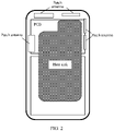
FIG. 2 is a schematic diagram of relative positions of a heat sink and patch antennas in an electronic device according to an embodiment of this application; -
FIG. 3 is a schematic structural diagram of an electronic device according to an embodiment of this application; -
FIG 4 is a schematic diagram of a cross section of a first region along a first direction; -
FIG. 5 is a schematic diagram of a cross section of the heat sink along a second direction; -
FIG. 6 is a diagram of simulation results of an antenna unit shown inFIG. 3 ; -
FIG. 7 is a schematic structural diagram of an antenna layout in an electronic device; -
FIG. 8 is a diagram of simulation results among antenna units shown inFIG. 7 ; -
FIG. 9 is a diagram of an electric field distribution corresponding to 2.64 GHz; -
FIG. 10 is a diagram of an electric field distribution corresponding to 3.5 GHz; -
FIG. 11 is a diagram of an electric field distribution corresponding to 4 GHz; -
FIG. 12 is a diagram of an electric field distribution corresponding to 4.7 GHz; -
FIG. 13 is a schematic structural diagram of all regions on a heat sink according to an embodiment of this application; -
FIG. 14 is a schematic structural diagram of an electronic device according to an embodiment of this application; -
FIG. 15 is a schematic structural diagram of an electronic device according to an embodiment of this application; -
FIG. 16 is a schematic structural diagram of an electronic device according to an embodiment of this application; -
FIG. 17 is a schematic structural diagram of an electronic device according to an embodiment of this application; and -
FIG. 18 is a schematic structural diagram of an electronic device according to an embodiment of this application. - The following describes technical solutions of this application with reference to accompanying drawings.
- It is to be understood that, in this application, "electrical connection" can be understood as physical contact and electrical conduction between components; and can also be understood as a form in which different components in a circuit construction are connected through physical circuits that can transmit an electrical signal, such as copper foil of a printed circuit board (printed circuit board, PCB), or wires. "Communication connection" may refer to transmission of the electrical signal, including wireless communication connection and wired communication connection. The wireless communication connection does not require a physical medium, and is not a connection relationship that defines a product construction. Both "connected to" and "connected with" may refer to a mechanical connection relationship or physical connection relationship, that is, that A is connected to B or that A is connected with B may refer to the fact that there is a fastened component between A and B (such as a screw, a bolt, and a rivet), or the fact that A and B are in contact with each other and A and B are difficult to be separated.
- The technical solutions provided in this application are applicable to an electronic device using one or more of the following communication technologies: blue tooth (blue tooth, BT) communication technology, global positioning system (global positioning system, GPS) communication technology, wireless fidelity (wireless fidelity, WiFi) communication technology, communication technology of global system for mobile communications (global system for mobile communications, GSM), wideband code division multiple access (wideband code division multiple access, WCDMA) communication technology, long term evolution (long term evolution, LTE) communication technology, 5G communication technology, and other communication technologies in the future. The electronic device in embodiments of this application may be a mobile phone, a tablet computer, a notebook computer, a smart bracelet, a smart watch, a smart helmet, smart glasses, and the like. The electronic device may alternatively be a cellular phone, a cordless phone, a session initiation protocol (session initiation protocol, SIP) phone, a wireless local loop (wireless local loop, WLL) station, a personal digital assistant (personal digital assistant, PDA), a handheld device having a wireless communication function, a computing device or another processing device connected to a wireless modem, an in-vehicle device, an electronic device in a 5G network, an electronic device in a future evolved public land mobile network (public land mobile network, PLMN), or the like, which is not limited in the embodiments of this application.
- For example,
FIG. 1 shows an internal environment of the electronic device provided in this application, and the description is provided using a mobile phone as the electronic device. - As shown in
FIG. 1 , anelectronic device 10 may include: a cover glass (cover glass) 13, a display (display) 15, a printed circuit board (printed circuit board, PCB) 17, a middle frame (middle frame) 19, and a rear cover (rear cover) 21. - The
cover glass 13 may be arranged close to thedisplay 15, and may be mainly configured to protect and dustproofing thedisplay 15. - Optionally, the
display 15 may be a liquid crystal display (liquid crystal display, LCD), a light emitting diode (light emitting diode, LED), an organic light-emitting diode (organic light-emitting diode, OLED), or the like, which is not limited in this application. - The printed
circuit board PCB 17 may use a flame-resistant material (FR-4) dielectric board, a Rogers (Rogers) dielectric board, a mixed dielectric board of Rogers and FR-4, or the like. FR-4 is a code name for a flame-resistant material grade, and the Rogers dielectric board is a high-frequency board. A metal layer can be arranged on a side of the printedcircuit board PCB 17 close to themiddle frame 19, and the metal layer can be formed through etching metal on a surface of thePCB 17. The metal layer can be configured to ground electronic components carried on the printedcircuit board PCB 17 to prevent electrical shock to a user or damage to the device. The metal layer may be referred to as a PCB ground. Not limited to the PCB ground, theelectronic device 10 can further have another ground for grounding, such as a metal middle frame or another metal plane in the electronic device. In addition, multiple electronic components are arranged on thePCB 17. The multiple electronic components include one or more of a processor, a power management module, a memory, a sensor, a SIM card interface, and the like, and these electronic components are also provided with metal inside or on a surface. Theelectronic device 10 may further include a battery, which is not shown herein. The battery may be arranged in themiddle frame 19, and the battery may separate thePCB 17 into a main board and a sub-board. The main board may be arranged between aframe 11 of themiddle frame 19 and an upper edge of the battery, and the sub-board may be arranged between themiddle frame 19 and a lower edge of the battery. The battery may also be provided with a metal layer inside or on a surface. - The
middle frame 19 mainly plays a supporting role of the whole device. Themiddle frame 19 may include theframe 11, and theframe 11 may be formed by a conductive material such as metal. Theframe 11 may extend around an outer periphery of theelectronic device 10 and thedisplay 15. Specifically, theframe 11 may surround four sides of thedisplay 15 to help fix thedisplay 15. In an implementation, theframe 11 made of a metal material can be directly used as a metal frame of theelectronic device 10 to form an appearance of the metal frame, which is suitable for metal industrial design (industrial design, ID). In another implementation, an outer surface of theframe 11 may alternatively be made of a non-metal material, and may be, for example, a plastic frame to form an appearance of a non-metal frame, which is suitable for non-metal ID. - The
rear cover 21 may be a rear cover made of a metal material, or may be a rear cover made of a non-conductive material, such as a glass rear cover, a plastic rear cover, or another non-metal rear cover. -
FIG. 1 only schematically shows some components included in theelectronic device 10. The actual shapes, actual dimensions, and actual constructions of these components are not limited inFIG. 1 . In addition, theelectronic device 10 may further include elements such as a camera and a sensor. - It is to be understood that, in this application, it can be considered that a surface on which the display of the electronic device is located is a front surface, a surface on which the rear cover is located is a back surface, and a surface on which the frame is located is a side surface.
- With the development of the 5G wireless communication system, the demand for the number of antennas greatly increases, and an antenna is required to be arranged on the back surface of the electronic device as shown in
FIG. 2 . The antenna arranged on the back surface of the electronic device is usually a patch (patch) antenna. In order not to affect radiation performance of the antenna, the rear cover of the electronic device begins to evolve towards a non-metal direction. However, power consumption of a chip corresponding to the 5G wireless communication system is about 2.5 times that of 4G, and the power consumption and heat generation amount during working rises sharply. Because the rear cover of the electronic device is non-metal, the heat dissipation effect is not good, and additional heat dissipation design is required. As shown inFIG. 2 , the heat generated by a high-temperature region (a region of the PCB where the chip is located) is transferred to a low-temperature region (a region where the battery is located) through the heat sink, so that the heat is evenly distributed. - It is to be understood that, for the patch antenna, a relatively large area is usually required to achieve relatively high over the air (over the air, OTA) performance and a relatively low electromagnetic wave specific absorption rate (specific absorption rate, SAR). However, due to a large area of the heat sink, the heat sink basically occupies most of the space of the back surface of the electronic device. The heat sink is usually made of materials such as graphite with high electrical conductivity. In a case that the heat sink overlaps with the patch antenna, the performance of the antenna is to be greatly affected.
- The embodiments of this application provide an antenna structure that can implement both a radiation characteristic of the antenna and heat dissipation performance of the heat sink, which effectively solves the contradiction between the two.
-
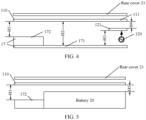
FIG. 3 to FIG. 5 are schematic structural diagrams of an electronic device according to an embodiment of this application.FIG. 3 is a schematic structural diagram of an electronic device according to an embodiment of this application.FIG 4 is a schematic diagram of a cross section of a first region along a first direction.FIG. 5 is a schematic diagram of a cross section of the heat sink along a second direction. - As shown in
FIG. 3 , the electronic device may include aheat sink 110, thePCB 17, abattery 20, and themiddle frame 19. ThePCB 17 and thebattery 20 may be arranged in a region enclosed by themiddle frame 19, one part of theheat sink 110 may be arranged above thePCB 17, and the other part of theheat sink 110 may be arranged above thebattery 20. Afeed point 111 may be arranged in afirst region 112 of theheat sink 110, and afeed unit 120 in the electronic device may be electrically connected to the heat sink at thefeed point 111. - It is to be understood that, the
heat sink 110 can distribute the heat in the electronic device evenly. Therefore, one part of the heat sink may be arranged above a heat source (the electronic elements on the PCB) and the other part may be arranged in a low-temperature region, to achieve the purpose of heat dissipation, or the part of heat sink may not be arranged between thebattery 20 and therear cover 21. A placement position of the heat sink can be adjusted according to an actual layout in the electronic device, which is not limited in this application. - As shown in
FIG. 4 , the electronic device may further include thefeed unit 120 and therear cover 21. The part of theheat sink 110 is arranged between thePCB 17 and therear cover 21. As shown inFIG. 5 , the part of theheat sink 110 is arranged between thebattery 20 and therear cover 21. The first direction may be a direction in which a short side of the frame of the electronic device is located. The second direction may be a direction in which a long side of the frame of the electronic device is located. - It is to be understood that, this embodiment of this application solves the problem of mutual influence between a heat dissipation component and the patch antenna in the electronic device by multiplexing the
heat sink 110. Theheat sink 110 provided by this embodiment of this application may be used as the heat dissipation component to transfer the heat generated by the high-temperature region (the region on the PCB where the chip is located) to the low-temperature region (the region where the battery is located) to distribute the heat evenly, thereby achieving the purpose of cooling down an overheated electronic element. In addition, theheat sink 110 can be used as a radiator of the antenna, to form an antenna unit with the feed unit and generate radiation to the outside. Theheat sink 110 in thefirst region 112 can be used as a main radiator of the antenna unit to meet the demand for the number of antennas in the 5G wireless communication system, and can also be applied to other communication systems. Optionally, the electronic device may further include acoupling member 121. Thefeed unit 120 may be electrically connected to thecoupling member 121, and provide indirect coupling feeding for the antenna unit at thefeed point 111. Alternatively, thefeed unit 120 may be connected to theheat sink 110 at thefeed point 111, and directly feed the antenna unit. - It is to be understood that, indirect coupling is a concept relative to direct coupling, that is, over-the-air coupling, and there is no direct electrical connection between two components. Direct coupling is a direct electrical connection, in which power is fed directly at the feed point. Optionally, the
coupling member 121 may be implemented in the manner of laser-direct-structuring (laser-direct-structuring, LDS), flexible printed circuit (flexible printed circuit, FPC) printing, or using floating metal (floating metal, FLM). - Optionally, as shown in
FIG. 3 , a dimension of theheat sink 110 can be adjusted according to actual production or design. In this embodiment of this application, a diagram of a simulation result in the following is illustrated by using an example in which a length L1 of theheat sink 110 is 98 mm and a width L2 of theheat sink 110 is 65 mm, while the specific dimension of theheat sink 110 is not limited. - Optionally, as shown in
FIG. 3 , the dimension of thefirst region 112 of theheat sink 110 can be adjusted according to the actual production and design. In this embodiment of this application, a diagram of a simulation result in the following is illustrated by using an example in which a length L3 of thefirst region 112 of theheat sink 110 is 24 mm and a width L4 of thefirst region 112 of theheat sink 110 is 16 mm, while the specific dimension of theheat sink 110 is not limited. In addition, a position of thefirst region 112 of theheat sink 110 can also be adjusted. In this embodiment of this application, thefirst region 112 is located in a boundary region of two sides of theheat sink 110 as an example. Alternatively, thefirst region 112 can be located in other positions of theheat sink 110, such as a center region. - Optionally, as shown in
FIG. 4 , thePCB 17 may include a shieldingcover 172 and ametal layer 171. Themetal layer 171 may be used as the ground (ground, GND) of the antenna unit, and the shieldingcover 172 is electrically connected to themetal layer 171, and is configured to prevent the electronic element in the shieldingcover 172 from external electromagnetic interference. Optionally, as shown inFIG. 4 and FIG. 5 , a distance H1 between the shieldingcover 172 and theheat sink 110 may be 0.2 mm, a distance H2 between themetal layer 171 and theheat sink 110 may be 0.8 mm, a distance H3 between thecoupling member 121 and themetal layer 171 may be 0.65 mm, a distance H4 between thecoupling member 121 and theheat sink 110 may be 0.15 mm, and a distance H5 between theheat sink 110 and thebattery 20 may be 0.1 mm. It is to be understood that, the foregoing data are only used as an example in the embodiments of this application, and can be adjusted according to the actual production and design. - Optionally, an insulation layer may be arranged on a surface of the
heat sink 110 close to thebattery 20 to avoid that theheat sink 110 is in directly contact with a metal component to reduce the performance of the antenna unit. - Optionally, the
heat sink 110 may be a graphite sheet, a copper sheet, or the like, and also has features of fast heat dissipation and high electrical conductivity. -
FIG. 6 is a diagram of simulation results of the antenna unit shown inFIG. 3 . The diagram includes simulation results of S parameter, radiation efficiency (radiation efficiency), and total efficiency (total efficiency). - As shown in
FIG. 6 , a working frequency band of the antenna unit formed by multiplexing the heat sink provided by this embodiment of this application can cover a frequency band of N41 (2.496 GHz to 2.69 GHz), a frequency band of N77 (3.3 GHz to 4.2 GHz), and a frequency band of N79 (4.4 GHz to 5.0 GHz). In addition, in the working frequency band corresponding to resonance generated by the antenna unit, the radiation efficiency and the total efficiency can also meet the demand. - It is to be understood that, in the technical solutions provided in the embodiments of this application, the heat sink is used as an antenna radiator. However, a radiation area of the heat sink is much larger than a working wavelength corresponding to the lowest working frequency band of the antenna unit.
-
FIG. 7 is a schematic structural diagram of an antenna layout in an electronic device. - As shown in
FIG. 7 , the electronic device may include anantenna unit 1, anantenna unit 2, anantenna unit 3, anantenna unit 4, and anantenna unit 5. - The
antenna unit 1 is a solution provided by the embodiments of this application in which the heat sink is used as an antenna radiator. Theantenna unit 2, theantenna unit 3, theantenna unit 4, and theantenna unit 5 are common metal frame antennas, which are only used as an example in this application. -
FIG. 8 is a diagram of simulation results among antenna units shown inFIG. 7 . - As shown in
FIG. 8 , S11 is an S parameter corresponding to theantenna unit 1, S22 is an S parameter corresponding to theantenna unit 2, S33 is an S parameter corresponding to theantenna unit 3, S44 is an S parameter corresponding to theantenna unit 4, and S55 is an S parameter corresponding to theantenna unit 5. Theantenna unit 1, theantenna unit 2, theantenna unit 3, theantenna unit 4, and theantenna unit 5 can all work in the corresponding working frequency bands, and good isolation can be maintained between theantenna unit 1 and theantenna unit 2, theantenna unit 3, theantenna unit 4, and theantenna unit 5. From the results, the worst isolation is -18 dB. -
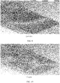
FIG. 9 to FIG. 12 are diagrams of an electric field distribution of the antenna unit shown inFIG. 3 .FIG. 9 is a diagram of an electric field distribution corresponding to 2.64 GHz.FIG. 10 is a diagram of an electric field distribution corresponding to 3.5 GHz.FIG. 11 is a diagram of an electric field distribution corresponding to 4 GHz.FIG. 12 is a diagram of an electric field distribution corresponding to 4.7 GHz. - As shown in
FIG. 9 , a resonant mode of the antenna unit at the frequency point 2.64 GHz in the N41 frequency band is a TM01 mode in the first region and the heat sink around the first region, and there is very little electric field distribution on the heat sink in the remaining region. - As shown in
FIG. 10 , the resonant mode of the antenna unit at the frequency point 3.5 GHz in the N77 frequency band is a TM10 mode in the first region and the heat sink around the first region, and there is very little electric field distribution on the heat sink in the remaining region. As shown inFIG. 11 , the resonant mode of the antenna unit at thefrequency point 4 GHz in the N77 frequency band is a TM11 mode of the heat sink in and around the first region, and there is strong electric field distribution on the heat sink along an edge region of the battery in the remaining region. - As shown in
FIG. 12 , the resonant mode of the antenna unit at the frequency point 4.7 GHz in the N79 frequency band is a TM02 mode of the heat sink in the first region and the heat sink around the first region, and there is electric field distribution of TM20 mode on the heat sink along the edge region of the battery in the remaining region. - It is to be understood that, as shown in
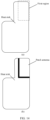
FIG. 13 , the heat sink in asecond region 112 on the left side of thefirst region 112 has a great influence on the TM01 mode, which is equivalent to an effect of shunt capacitance, causing the TM01 mode to be low. The heat sink has some influence on other modes as well. The heat sink in athird region 114 arranged along the side edge of the battery has a great influence on the TM10 mode and higher-order mode, which is equivalent to the effect of the shunt capacitance, causing the resonance to be low. The heat sink in afourth region 115 arranged along the upper edge of the battery basically has no radiation effect and has a shunting effect in the TM01/TM10/TM11 mode. The current distribution is relatively strong in the TM02 mode. -
FIG. 14 is a schematic structural diagram of an electronic device according to an embodiment of this application. - As shown in
FIG. 14(a) , in the technical solution provided by this application, the heat sink is used as the antenna radiator. As shown inFIG. 14(b) , a technical solution in conventional technology is used as a comparison solution of this application, in which a patch antenna corresponding to the first region is selected, which is not in contact with the heat sink. - As shown in Table 1 below, Table 1 shows the SAR value corresponding to back (back) 0 mm and 5 mm of the electronic device in a case that a normalized total radiated power (total radiated power, TRP) of the antenna unit shown in
FIG. 14(a) is 19 dB.Table 1 Technical solution in FIG. 14(a) Normalized SAR value Back 0 mm Back 5 mm Frequency (GHz) Normalized TRP (dB) 10g 1g 10g 1g 2.77 19 5.1 15.4 3.5 9.3 3.4 19 4.6 14.3 2.8 6.9 4.6 19 4.9 18.6 1.3 3.9 4.9 19 4.9 19 1.2 3.7 - As shown in Table 2 below, Table 2 shows the SAR value corresponding to back (back) 0 mm and 5 mm of the electronic device in a case that the normalized TRP of the antenna unit shown in
FIG. 14(b) is 19 dB.Table 2 Technical solution in FIG. 14(b) Normalized SAR value Back 0 mm Back 5 mm Frequency (GHz) Normalized TRP (dB) 10g 1g 10g 1g 3.4 19 7.1 22.2 5.1 16.3 3.82 19 5.2 15.7 3.3 9.3 4.58 19 4.9 21.8 1.4 4.6 5 19 5.2 21.8 1.9 6.4 - As shown in the above tables, the technical solution provided by this application has a significantly lower SAR value and better performance compared to the related art. This is because the heat sink outside the first region plays a role of shunting.
- As shown in Table 3 below, Table 3 shows the performance of the antenna unit shown in
FIG. 14(a) in a hand left (hand left, HL) model, a hand right (hand right, HR) model, a beside head and hand left (beside head and hand left, BHHL) model, and a beside head and hand right (beside head and hand right, BHHR) model.Table 3 Frequency (GHz) HR (GHz) HL (GHz) BHHR (GHz) BHHL (GHz) 2.65 -0.4 -0.7 -1.2 -1.7 3.3 -0.7 -0.7 -1 -1 3.8 -0.5 -0.5 -1 -0.7 4.2 -1.5 -1.5 -2 -2.2 4.5 -0.5 -0.5 -1.5 -1.5 5 -0.5 -0.5 -1.3 -1 - As shown in Table 4 below, Table 4 shows the performance of the antenna unit shown in
FIG. 14(b) in the HL model, the HR model, the BHHL model, and the BHHR model.Table 4 Frequency (GHz) HR (GHz) HL (GHz) BHHR (GHz) BHHL (GHz) 3.3 -0.5 -0.5 -1 -0.5 3.8 -1.2 -0.5 -2 -1.5 4.2 -0.5 0.5 -0.5 -0.5 4.5 -0.5 -0.3 -0.5 -0.5 5 -0.5 -0.5 -1 -1 - As shown in the above tables, the technical solution provided by this application has similar performance to the related art, and the head-hand performance of the technical solution provided by this application does not become poor due to the enlarged antenna radiator.
-
FIG. 15 is a schematic structural diagram of an electronic device according to an embodiment of this application. - The electronic device may include a first feed unit, a second feed unit, and a third feed unit.
- As shown in
FIG. 15 , aheat sink 200 may be provided with afirst feed point 201, asecond feed point 202, and athird feed point 203. The first feed unit may be electrically connected to theheat sink 200 at thefirst feed point 201. The second feed unit may be electrically connected to theheat sink 200 at thesecond feed point 202. The third feed unit may be electrically connected to theheat sink 200 at thethird feed point 203. - It is to be understood that, the first feed unit and the heat sink form a first antenna unit, the second feed unit and the heat sink form a second antenna unit, and the third feed unit and the heat sink form a third antenna unit. The heat sink is a complete plane, and is not spliced by several parts. The first antenna unit, the second feed unit, and the third antenna unit share the same radiator, but their corresponding main radiation parts are different.
- In addition, the number of the feed point can be adjusted according to the actual design or production. This application only takes three feed points as an example, and the specific number of the feed point is not limited in this application.
-
FIG. 16 is a schematic structural diagram of an electronic device according to an embodiment of this application. - As shown in
FIG. 16 , aheat sink 300 may be provided with afirst ground point 301 and asecond ground point 302. Theheat sink 300 may be electrically connected to a ground of the electronic device at thefirst ground point 301 and thesecond ground point 302. - Optionally, the ground of the electronic device may be a metal layer in the PCB, the middle frame, or another metal layer of the electronic device.
- Optionally, the heat sink may be electrically connected to the ground at the ground point through indirect coupling. Alternatively, the heat sink may be directly connected to the ground at the ground point directly.
- It is to be understood that, by arranging the ground point on the
heat sink 300, a current direction on theheat sink 300 can be effectively changed, thereby affecting the radiation characteristic of the antenna unit formed by the heat sink. Therefore, the number of the ground point can be adjusted according to the actual design or production. This application only takes two ground points as an example, and the specific number of the ground point is not limited in this application. -
FIG. 17 is a schematic structural diagram of an electronic device according to an embodiment of this application. - As shown in
FIG. 17 , aheat sink 400 may be provided with afirst gap 401, asecond gap 402, and athird gap 403. - Optionally, the gap on the
heat sink 400 may be an open gap, or may be a closed gap, which is not limited in this application. - It is to be understood that, by arranging the gap on the
heat sink 400, a current path can be blocked to change a current direction on theheat sink 400, thereby affecting the radiation characteristic of the antenna unit formed by the heat sink. Therefore, the dimension, position, and number of the gap can be adjusted according to the actual design or production. This application only takes three gaps as an example, while the specific dimension, position, and number of the gap are not limited in this application. -
FIG. 18 is a schematic structural diagram of an electronic device according to an embodiment of this application. - As shown in
FIG. 18 , the electronic device may further include afirst metal member 501 and asecond metal member 502, and thefirst metal member 501 and thesecond metal member 502 can be arranged above the heat sink. For example, thefirst metal member 501 and thesecond metal member 502 may be arranged between the heat sink and the PCB, or between the heat sink and the battery, or between the heat sink and the rear cover, or on a surface of the rear cover away from the heat sink, that is, at a certain distance from the heat sink in a third direction. The third direction is a direction perpendicular to a plane where the rear cover is located. - It is to be understood that, by arranging the metal member around a
heat sink 500, a current direction on theheat sink 500 can be changed through the indirect coupling of the metal member, thereby affecting the radiation characteristic of the antenna unit formed by the heat sink. Therefore, the dimension, position, and number of the metal member can be adjusted according to the actual design or production. This application only takes two metal members as an example, and the specific dimension, position, and number of the metal member is not limited in this application. - A person skilled in the art can clearly understand that for convenience and conciseness of description, the specific working processes of the above-described system, apparatus, and unit can be understood with reference to the corresponding processes in the above-described method embodiments, and details are not repeated herein again.
- In the several embodiments provided in this application, it is to be understood that the disclosed system, apparatus, and method may be implemented in other manners. For example, the above-described apparatus embodiment is only exemplary. For example, the division of the units is only a logical function division and may be other divisions during actual implementation. For example, a plurality of units or components may be combined or integrated into another system, or some features may be ignored or not performed. In addition, the shown or discussed mutual couplings or direct couplings or communication connections may be implemented through some interfaces. The indirect couplings or communication connections between the apparatuses or units may be implemented in electronic, mechanical, or other forms.
- The foregoing descriptions are merely specific implementations of this application, but are not intended to limit the protection scope of this application. Any variation or replacement readily figured out by a person skilled in the art within the technical scope disclosed in this application shall fall within the protection scope of this application. Therefore, the protection scope of this application shall be subjected to the protection scope of the claims.
Claims (11)
- An electronic device, comprising:a heat sink, a first feed unit, a printed circuit board PCB, a middle frame, and a rear cover, whereinthe PCB is arranged in a space enclosed by the middle frame and the rear cover;part of the heat sink is arranged between the PCB and the rear cover; andthe heat sink is provided with a first feed point, and the first feed unit is electrically connected to the heat sink at the first feed point.
- The electronic device according to claim 1, further comprising: a battery, whereinthe battery is arranged in the space enclosed by the middle frame and the rear cover; andthe part of the heat sink is arranged between the battery and the rear cover.
- The electronic device according to claim 1,further comprising a second feed unit, whereinthe heat sink is provided with a second feed point, and the second feed unit is electrically connected to the heat sink at the second feed point.
- The electronic device according to claim 3,further comprising a ground, whereinthe heat sink is provided with a first ground point, and the heat sink is electrically connected to the ground at the first ground point.
- The electronic device according to claim 4, wherein that the heat sink is electrically connected to the ground at the first ground point comprises: the heat sink is directly connected to or indirectly coupled to the ground at the first ground point.
- The electronic device according to claim 3, wherein the heat sink is provided with a gap.
- The electronic device according to claim 6, wherein the gap is an open gap or a closed gap.
- The electronic device according to claim 2,further comprising a metal member, whereinthe metal member is arranged above the heat sink.
- The electronic device according to claim 8, wherein that the metal member is arranged above the heat sink comprises:
the metal member is arranged between the heat sink and the PCB, or between the heat sink and the battery, or between the heat sink and the rear cover, or on a surface of the rear cover away from the heat sink. - The electronic device according to any one of claims 1 to 9, wherein that the first feed unit is electrically connected to the heat sink at the first feed point comprises: the first feed unit is directly connected to or indirectly coupled to the heat sink at the first feed point.
- The electronic device according to claim 10,further comprising a coupling member, whereinthe first feed unit is electrically connected to the coupling member, and the coupling member provides indirect coupling feeding at the first feed point for an antenna unit formed by the first feed unit and the heat sink.
Applications Claiming Priority (2)
| Application Number | Priority Date | Filing Date | Title |
|---|---|---|---|
| CN202023019475.5U CN214627565U (en) | 2020-12-15 | 2020-12-15 | Electronic equipment |
| PCT/CN2021/114443 WO2022127175A1 (en) | 2020-12-15 | 2021-08-25 | Electronic device |
Publications (3)
| Publication Number | Publication Date |
|---|---|
| EP4156876A1 true EP4156876A1 (en) | 2023-03-29 |
| EP4156876A4 EP4156876A4 (en) | 2024-01-03 |
| EP4156876B1 EP4156876B1 (en) | 2025-06-11 |
Family
ID=78429521
Family Applications (1)
| Application Number | Title | Priority Date | Filing Date |
|---|---|---|---|
| EP21905108.3A Active EP4156876B1 (en) | 2020-12-15 | 2021-08-25 | Electronic device |
Country Status (4)
| Country | Link |
|---|---|
| US (1) | US12368795B2 (en) |
| EP (1) | EP4156876B1 (en) |
| CN (1) | CN214627565U (en) |
| WO (1) | WO2022127175A1 (en) |
Families Citing this family (7)
| Publication number | Priority date | Publication date | Assignee | Title |
|---|---|---|---|---|
| CN114914666B (en) | 2021-02-10 | 2024-03-26 | 华为技术有限公司 | Antenna and electronic equipment |
| CN115548647A (en) * | 2021-06-30 | 2022-12-30 | 华为技术有限公司 | Microstrip antenna and electronic equipment |
| CN115693111B (en) * | 2021-07-26 | 2025-10-24 | 华为技术有限公司 | An electronic device |
| CN117560842A (en) * | 2022-08-03 | 2024-02-13 | 华为技术有限公司 | Electronic equipment |
| CN117855813A (en) * | 2022-10-01 | 2024-04-09 | 华为终端有限公司 | Electronic equipment |
| WO2024225807A1 (en) * | 2023-04-26 | 2024-10-31 | 삼성전자 주식회사 | Electronic device comprising thermal diffusion member |
| CN220755126U (en) * | 2023-08-09 | 2024-04-09 | 华为技术有限公司 | Electronic equipment and radiator |
Family Cites Families (11)
| Publication number | Priority date | Publication date | Assignee | Title |
|---|---|---|---|---|
| KR101137581B1 (en) * | 2005-12-19 | 2012-04-19 | 엘지전자 주식회사 | Portable terminal |
| CN101031197A (en) * | 2006-03-02 | 2007-09-05 | 华硕电脑股份有限公司 | Electronic device with electromagnetic interference suppression function and heat dissipation component thereof |
| KR102226173B1 (en) | 2014-09-02 | 2021-03-10 | 삼성전자주식회사 | Antenna using exterior metal frame and electronic device therewith |
| US10431868B2 (en) | 2017-05-24 | 2019-10-01 | Plume Design, Inc. | Antenna structure incorporated in heat spreader, heat sink, and cooling fins |
| CN107249283B (en) * | 2017-07-12 | 2019-07-12 | 普联技术有限公司 | A kind of mobile terminal |
| US11276654B2 (en) * | 2019-12-17 | 2022-03-15 | Nxp Usa, Inc. | Bottom-side heatsinking waveguide for an integrated circuit package |
| CN113140884B (en) * | 2020-01-20 | 2023-05-16 | 北京小米移动软件有限公司 | Heat radiation structure and terminal equipment with signal transmission function |
| CN114498005B (en) * | 2020-06-02 | 2023-01-10 | Oppo广东移动通信有限公司 | Customer Pre-equipment |
| CN112055507A (en) * | 2020-06-16 | 2020-12-08 | 努比亚技术有限公司 | Heat dissipation device and terminal |
| CN112739174A (en) * | 2021-01-08 | 2021-04-30 | 惠州Tcl移动通信有限公司 | Mobile terminal heat radiation structure |
| CN112909475B (en) * | 2021-01-15 | 2023-12-12 | Oppo广东移动通信有限公司 | Antenna assembly and electronic equipment |
-
2020
- 2020-12-15 CN CN202023019475.5U patent/CN214627565U/en active Active
-
2021
- 2021-08-25 WO PCT/CN2021/114443 patent/WO2022127175A1/en not_active Ceased
- 2021-08-25 EP EP21905108.3A patent/EP4156876B1/en active Active
- 2021-08-25 US US18/001,753 patent/US12368795B2/en active Active
Also Published As
| Publication number | Publication date |
|---|---|
| US20230232587A1 (en) | 2023-07-20 |
| US12368795B2 (en) | 2025-07-22 |
| CN214627565U (en) | 2021-11-05 |
| EP4156876B1 (en) | 2025-06-11 |
| WO2022127175A1 (en) | 2022-06-23 |
| EP4156876A4 (en) | 2024-01-03 |
Similar Documents
| Publication | Publication Date | Title |
|---|---|---|
| EP4156876B1 (en) | Electronic device | |
| EP4148905A1 (en) | Electronic device | |
| US12322875B2 (en) | Antenna structure and electronic device | |
| JP7581506B2 (en) | Electronic Devices | |
| CN108539386B (en) | An antenna structure and wireless terminal | |
| CN113948857B (en) | Electronic equipment | |
| CN115693111B (en) | An electronic device | |
| US10483622B2 (en) | Antenna structure and wireless communication device using same | |
| CN113555692B (en) | an electronic device | |
| US20190252765A1 (en) | Antenna structure and wireless communication device using the same | |
| WO2023246694A1 (en) | Electronic device | |
| CN114389006B (en) | Electronic equipment | |
| US20200343637A1 (en) | Antenna and terminal | |
| CN213959134U (en) | an electronic device | |
| CN115696839B (en) | Electronic equipment and preparation method of graphene film | |
| EP4362227A1 (en) | Antenna structure and electronic device | |
| CN114256595A (en) | Electronic equipment | |
| TWI571002B (en) | Antenna device and communication device using the same | |
| WO2022151826A1 (en) | Antenna apparatus and electronic device | |
| EP4542770A1 (en) | Electronic device |
Legal Events
| Date | Code | Title | Description |
|---|---|---|---|
| STAA | Information on the status of an ep patent application or granted ep patent |
Free format text: STATUS: THE INTERNATIONAL PUBLICATION HAS BEEN MADE |
|
| PUAI | Public reference made under article 153(3) epc to a published international application that has entered the european phase |
Free format text: ORIGINAL CODE: 0009012 |
|
| STAA | Information on the status of an ep patent application or granted ep patent |
Free format text: STATUS: REQUEST FOR EXAMINATION WAS MADE |
|
| 17P | Request for examination filed |
Effective date: 20221219 |
|
| AK | Designated contracting states |
Kind code of ref document: A1 Designated state(s): AL AT BE BG CH CY CZ DE DK EE ES FI FR GB GR HR HU IE IS IT LI LT LU LV MC MK MT NL NO PL PT RO RS SE SI SK SM TR |
|
| REG | Reference to a national code |
Ref country code: DE Free format text: PREVIOUS MAIN CLASS: H05K0005020000 Ref country code: DE Ref legal event code: R079 Ref document number: 602021032273 Country of ref document: DE Free format text: PREVIOUS MAIN CLASS: H05K0005020000 Ipc: H01Q0001020000 |
|
| A4 | Supplementary search report drawn up and despatched |
Effective date: 20231205 |
|
| RIC1 | Information provided on ipc code assigned before grant |
Ipc: H05K 7/20 20060101ALI20231129BHEP Ipc: H04M 1/02 20060101ALI20231129BHEP Ipc: H01Q 1/44 20060101ALI20231129BHEP Ipc: H01Q 1/24 20060101ALI20231129BHEP Ipc: H01Q 1/02 20060101AFI20231129BHEP |
|
| DAV | Request for validation of the european patent (deleted) | ||
| DAX | Request for extension of the european patent (deleted) | ||
| STAA | Information on the status of an ep patent application or granted ep patent |
Free format text: STATUS: EXAMINATION IS IN PROGRESS |
|
| 17Q | First examination report despatched |
Effective date: 20240625 |
|
| R17C | First examination report despatched (corrected) |
Effective date: 20240625 |
|
| GRAP | Despatch of communication of intention to grant a patent |
Free format text: ORIGINAL CODE: EPIDOSNIGR1 |
|
| STAA | Information on the status of an ep patent application or granted ep patent |
Free format text: STATUS: GRANT OF PATENT IS INTENDED |
|
| INTG | Intention to grant announced |
Effective date: 20250107 |
|
| GRAS | Grant fee paid |
Free format text: ORIGINAL CODE: EPIDOSNIGR3 |
|
| GRAA | (expected) grant |
Free format text: ORIGINAL CODE: 0009210 |
|
| STAA | Information on the status of an ep patent application or granted ep patent |
Free format text: STATUS: THE PATENT HAS BEEN GRANTED |
|
| AK | Designated contracting states |
Kind code of ref document: B1 Designated state(s): AL AT BE BG CH CY CZ DE DK EE ES FI FR GB GR HR HU IE IS IT LI LT LU LV MC MK MT NL NO PL PT RO RS SE SI SK SM TR |
|
| REG | Reference to a national code |
Ref country code: GB Ref legal event code: FG4D |
|
| REG | Reference to a national code |
Ref country code: CH Ref legal event code: EP |
|
| REG | Reference to a national code |
Ref country code: IE Ref legal event code: FG4D |
|
| REG | Reference to a national code |
Ref country code: DE Ref legal event code: R096 Ref document number: 602021032273 Country of ref document: DE |
|
| REG | Reference to a national code |
Ref country code: NL Ref legal event code: FP |
|
| PGFP | Annual fee paid to national office [announced via postgrant information from national office to epo] |
Ref country code: NL Payment date: 20250704 Year of fee payment: 5 |
|
| PG25 | Lapsed in a contracting state [announced via postgrant information from national office to epo] |
Ref country code: ES Free format text: LAPSE BECAUSE OF FAILURE TO SUBMIT A TRANSLATION OF THE DESCRIPTION OR TO PAY THE FEE WITHIN THE PRESCRIBED TIME-LIMIT Effective date: 20250611 Ref country code: FI Free format text: LAPSE BECAUSE OF FAILURE TO SUBMIT A TRANSLATION OF THE DESCRIPTION OR TO PAY THE FEE WITHIN THE PRESCRIBED TIME-LIMIT Effective date: 20250611 |
|
| PGFP | Annual fee paid to national office [announced via postgrant information from national office to epo] |
Ref country code: DE Payment date: 20250702 Year of fee payment: 5 |
|
| REG | Reference to a national code |
Ref country code: LT Ref legal event code: MG9D |
|
| PG25 | Lapsed in a contracting state [announced via postgrant information from national office to epo] |
Ref country code: GR Free format text: LAPSE BECAUSE OF FAILURE TO SUBMIT A TRANSLATION OF THE DESCRIPTION OR TO PAY THE FEE WITHIN THE PRESCRIBED TIME-LIMIT Effective date: 20250912 Ref country code: NO Free format text: LAPSE BECAUSE OF FAILURE TO SUBMIT A TRANSLATION OF THE DESCRIPTION OR TO PAY THE FEE WITHIN THE PRESCRIBED TIME-LIMIT Effective date: 20250911 |
|
| PG25 | Lapsed in a contracting state [announced via postgrant information from national office to epo] |
Ref country code: BG Free format text: LAPSE BECAUSE OF FAILURE TO SUBMIT A TRANSLATION OF THE DESCRIPTION OR TO PAY THE FEE WITHIN THE PRESCRIBED TIME-LIMIT Effective date: 20250611 |
|
| PGFP | Annual fee paid to national office [announced via postgrant information from national office to epo] |
Ref country code: GB Payment date: 20250703 Year of fee payment: 5 |
|
| PG25 | Lapsed in a contracting state [announced via postgrant information from national office to epo] |
Ref country code: HR Free format text: LAPSE BECAUSE OF FAILURE TO SUBMIT A TRANSLATION OF THE DESCRIPTION OR TO PAY THE FEE WITHIN THE PRESCRIBED TIME-LIMIT Effective date: 20250611 |
|
| PGFP | Annual fee paid to national office [announced via postgrant information from national office to epo] |
Ref country code: AT Payment date: 20251020 Year of fee payment: 5 |
|
| PG25 | Lapsed in a contracting state [announced via postgrant information from national office to epo] |
Ref country code: RS Free format text: LAPSE BECAUSE OF FAILURE TO SUBMIT A TRANSLATION OF THE DESCRIPTION OR TO PAY THE FEE WITHIN THE PRESCRIBED TIME-LIMIT Effective date: 20250911 |
|
| PG25 | Lapsed in a contracting state [announced via postgrant information from national office to epo] |
Ref country code: LV Free format text: LAPSE BECAUSE OF FAILURE TO SUBMIT A TRANSLATION OF THE DESCRIPTION OR TO PAY THE FEE WITHIN THE PRESCRIBED TIME-LIMIT Effective date: 20250611 |
|
| PG25 | Lapsed in a contracting state [announced via postgrant information from national office to epo] |
Ref country code: PT Free format text: LAPSE BECAUSE OF FAILURE TO SUBMIT A TRANSLATION OF THE DESCRIPTION OR TO PAY THE FEE WITHIN THE PRESCRIBED TIME-LIMIT Effective date: 20251013 |
|
| REG | Reference to a national code |
Ref country code: AT Ref legal event code: MK05 Ref document number: 1803008 Country of ref document: AT Kind code of ref document: T Effective date: 20250611 |
|
| PG25 | Lapsed in a contracting state [announced via postgrant information from national office to epo] |
Ref country code: IS Free format text: LAPSE BECAUSE OF FAILURE TO SUBMIT A TRANSLATION OF THE DESCRIPTION OR TO PAY THE FEE WITHIN THE PRESCRIBED TIME-LIMIT Effective date: 20251011 |
|
| PG25 | Lapsed in a contracting state [announced via postgrant information from national office to epo] |
Ref country code: AT Free format text: LAPSE BECAUSE OF FAILURE TO SUBMIT A TRANSLATION OF THE DESCRIPTION OR TO PAY THE FEE WITHIN THE PRESCRIBED TIME-LIMIT Effective date: 20250611 Ref country code: SM Free format text: LAPSE BECAUSE OF FAILURE TO SUBMIT A TRANSLATION OF THE DESCRIPTION OR TO PAY THE FEE WITHIN THE PRESCRIBED TIME-LIMIT Effective date: 20250611 |
|
| PG25 | Lapsed in a contracting state [announced via postgrant information from national office to epo] |
Ref country code: CZ Free format text: LAPSE BECAUSE OF FAILURE TO SUBMIT A TRANSLATION OF THE DESCRIPTION OR TO PAY THE FEE WITHIN THE PRESCRIBED TIME-LIMIT Effective date: 20250611 |
|
| PG25 | Lapsed in a contracting state [announced via postgrant information from national office to epo] |
Ref country code: PL Free format text: LAPSE BECAUSE OF FAILURE TO SUBMIT A TRANSLATION OF THE DESCRIPTION OR TO PAY THE FEE WITHIN THE PRESCRIBED TIME-LIMIT Effective date: 20250611 |
|
| PG25 | Lapsed in a contracting state [announced via postgrant information from national office to epo] |
Ref country code: EE Free format text: LAPSE BECAUSE OF FAILURE TO SUBMIT A TRANSLATION OF THE DESCRIPTION OR TO PAY THE FEE WITHIN THE PRESCRIBED TIME-LIMIT Effective date: 20250611 |
|
| PG25 | Lapsed in a contracting state [announced via postgrant information from national office to epo] |
Ref country code: SK Free format text: LAPSE BECAUSE OF FAILURE TO SUBMIT A TRANSLATION OF THE DESCRIPTION OR TO PAY THE FEE WITHIN THE PRESCRIBED TIME-LIMIT Effective date: 20250611 |
|
| PG25 | Lapsed in a contracting state [announced via postgrant information from national office to epo] |
Ref country code: RO Free format text: LAPSE BECAUSE OF FAILURE TO SUBMIT A TRANSLATION OF THE DESCRIPTION OR TO PAY THE FEE WITHIN THE PRESCRIBED TIME-LIMIT Effective date: 20250611 |
|
| REG | Reference to a national code |
Ref country code: DE Ref legal event code: R097 Ref document number: 602021032273 Country of ref document: DE |
|
| REG | Reference to a national code |
Ref country code: CH Ref legal event code: H13 Free format text: ST27 STATUS EVENT CODE: U-0-0-H10-H13 (AS PROVIDED BY THE NATIONAL OFFICE) Effective date: 20260324 |
|
| PG25 | Lapsed in a contracting state [announced via postgrant information from national office to epo] |
Ref country code: MC Free format text: LAPSE BECAUSE OF FAILURE TO SUBMIT A TRANSLATION OF THE DESCRIPTION OR TO PAY THE FEE WITHIN THE PRESCRIBED TIME-LIMIT Effective date: 20250611 |
|
| PG25 | Lapsed in a contracting state [announced via postgrant information from national office to epo] |
Ref country code: DK Free format text: LAPSE BECAUSE OF FAILURE TO SUBMIT A TRANSLATION OF THE DESCRIPTION OR TO PAY THE FEE WITHIN THE PRESCRIBED TIME-LIMIT Effective date: 20250611 |
|
| PG25 | Lapsed in a contracting state [announced via postgrant information from national office to epo] |
Ref country code: LU Free format text: LAPSE BECAUSE OF NON-PAYMENT OF DUE FEES Effective date: 20250825 Ref country code: IT Free format text: LAPSE BECAUSE OF FAILURE TO SUBMIT A TRANSLATION OF THE DESCRIPTION OR TO PAY THE FEE WITHIN THE PRESCRIBED TIME-LIMIT Effective date: 20250611 |
|
| PLBE | No opposition filed within time limit |
Free format text: ORIGINAL CODE: 0009261 |
|
| STAA | Information on the status of an ep patent application or granted ep patent |
Free format text: STATUS: NO OPPOSITION FILED WITHIN TIME LIMIT |
|
| PG25 | Lapsed in a contracting state [announced via postgrant information from national office to epo] |
Ref country code: CH Free format text: LAPSE BECAUSE OF NON-PAYMENT OF DUE FEES Effective date: 20250831 |
|
| REG | Reference to a national code |
Ref country code: CH Ref legal event code: L10 Free format text: ST27 STATUS EVENT CODE: U-0-0-L10-L00 (AS PROVIDED BY THE NATIONAL OFFICE) Effective date: 20260423 |