EP4156872B1 - Electronic device comprising a camera module - Google Patents
Electronic device comprising a camera module Download PDFInfo
- Publication number
- EP4156872B1 EP4156872B1 EP21827886.9A EP21827886A EP4156872B1 EP 4156872 B1 EP4156872 B1 EP 4156872B1 EP 21827886 A EP21827886 A EP 21827886A EP 4156872 B1 EP4156872 B1 EP 4156872B1
- Authority
- EP
- European Patent Office
- Prior art keywords
- region
- circuit board
- electronic device
- flexible substrate
- conductive
- Prior art date
- Legal status (The legal status is an assumption and is not a legal conclusion. Google has not performed a legal analysis and makes no representation as to the accuracy of the status listed.)
- Active
Links
Images










Classifications
-
- H—ELECTRICITY
- H05—ELECTRIC TECHNIQUES NOT OTHERWISE PROVIDED FOR
- H05K—PRINTED CIRCUITS; CASINGS OR CONSTRUCTIONAL DETAILS OF ELECTRIC APPARATUS; MANUFACTURE OF ASSEMBLAGES OF ELECTRICAL COMPONENTS
- H05K1/00—Printed circuits
- H05K1/02—Details
- H05K1/11—Printed elements for providing electric connections to or between printed circuits
- H05K1/118—Printed elements for providing electric connections to or between printed circuits specially for flexible printed circuits, e.g. using folded portions
-
- H—ELECTRICITY
- H04—ELECTRIC COMMUNICATION TECHNIQUE
- H04N—PICTORIAL COMMUNICATION, e.g. TELEVISION
- H04N23/00—Cameras or camera modules comprising electronic image sensors; Control thereof
- H04N23/50—Constructional details
- H04N23/54—Mounting of pick-up tubes, electronic image sensors, deviation or focusing coils
-
- H—ELECTRICITY
- H04—ELECTRIC COMMUNICATION TECHNIQUE
- H04N—PICTORIAL COMMUNICATION, e.g. TELEVISION
- H04N23/00—Cameras or camera modules comprising electronic image sensors; Control thereof
- H04N23/57—Mechanical or electrical details of cameras or camera modules specially adapted for being embedded in other devices
-
- H—ELECTRICITY
- H05—ELECTRIC TECHNIQUES NOT OTHERWISE PROVIDED FOR
- H05K—PRINTED CIRCUITS; CASINGS OR CONSTRUCTIONAL DETAILS OF ELECTRIC APPARATUS; MANUFACTURE OF ASSEMBLAGES OF ELECTRICAL COMPONENTS
- H05K1/00—Printed circuits
- H05K1/02—Details
- H05K1/11—Printed elements for providing electric connections to or between printed circuits
- H05K1/111—Pads for surface mounting, e.g. lay-out
-
- H—ELECTRICITY
- H05—ELECTRIC TECHNIQUES NOT OTHERWISE PROVIDED FOR
- H05K—PRINTED CIRCUITS; CASINGS OR CONSTRUCTIONAL DETAILS OF ELECTRIC APPARATUS; MANUFACTURE OF ASSEMBLAGES OF ELECTRICAL COMPONENTS
- H05K1/00—Printed circuits
- H05K1/02—Details
- H05K1/11—Printed elements for providing electric connections to or between printed circuits
- H05K1/115—Via connections; Lands around holes or via connections
-
- H—ELECTRICITY
- H05—ELECTRIC TECHNIQUES NOT OTHERWISE PROVIDED FOR
- H05K—PRINTED CIRCUITS; CASINGS OR CONSTRUCTIONAL DETAILS OF ELECTRIC APPARATUS; MANUFACTURE OF ASSEMBLAGES OF ELECTRICAL COMPONENTS
- H05K1/00—Printed circuits
- H05K1/02—Details
- H05K1/14—Structural association of two or more printed circuits
- H05K1/147—Structural association of two or more printed circuits at least one of the printed circuits being bent or folded, e.g. by using a flexible printed circuit
-
- H—ELECTRICITY
- H04—ELECTRIC COMMUNICATION TECHNIQUE
- H04N—PICTORIAL COMMUNICATION, e.g. TELEVISION
- H04N23/00—Cameras or camera modules comprising electronic image sensors; Control thereof
- H04N23/60—Control of cameras or camera modules
- H04N23/68—Control of cameras or camera modules for stable pick-up of the scene, e.g. compensating for camera body vibrations
- H04N23/682—Vibration or motion blur correction
- H04N23/685—Vibration or motion blur correction performed by mechanical compensation
-
- H—ELECTRICITY
- H05—ELECTRIC TECHNIQUES NOT OTHERWISE PROVIDED FOR
- H05K—PRINTED CIRCUITS; CASINGS OR CONSTRUCTIONAL DETAILS OF ELECTRIC APPARATUS; MANUFACTURE OF ASSEMBLAGES OF ELECTRICAL COMPONENTS
- H05K1/00—Printed circuits
- H05K1/02—Details
- H05K1/14—Structural association of two or more printed circuits
- H05K1/144—Stacked arrangements of planar printed circuit boards
-
- H—ELECTRICITY
- H05—ELECTRIC TECHNIQUES NOT OTHERWISE PROVIDED FOR
- H05K—PRINTED CIRCUITS; CASINGS OR CONSTRUCTIONAL DETAILS OF ELECTRIC APPARATUS; MANUFACTURE OF ASSEMBLAGES OF ELECTRICAL COMPONENTS
- H05K2201/00—Indexing scheme relating to printed circuits covered by H05K1/00
- H05K2201/05—Flexible printed circuits [FPCs]
- H05K2201/052—Branched
-
- H—ELECTRICITY
- H05—ELECTRIC TECHNIQUES NOT OTHERWISE PROVIDED FOR
- H05K—PRINTED CIRCUITS; CASINGS OR CONSTRUCTIONAL DETAILS OF ELECTRIC APPARATUS; MANUFACTURE OF ASSEMBLAGES OF ELECTRICAL COMPONENTS
- H05K2201/00—Indexing scheme relating to printed circuits covered by H05K1/00
- H05K2201/05—Flexible printed circuits [FPCs]
- H05K2201/053—Tails
-
- H—ELECTRICITY
- H05—ELECTRIC TECHNIQUES NOT OTHERWISE PROVIDED FOR
- H05K—PRINTED CIRCUITS; CASINGS OR CONSTRUCTIONAL DETAILS OF ELECTRIC APPARATUS; MANUFACTURE OF ASSEMBLAGES OF ELECTRICAL COMPONENTS
- H05K2201/00—Indexing scheme relating to printed circuits covered by H05K1/00
- H05K2201/10—Details of components or other objects attached to or integrated in a printed circuit board
- H05K2201/10007—Types of components
- H05K2201/10121—Optical component, e.g. opto-electronic component
-
- H—ELECTRICITY
- H05—ELECTRIC TECHNIQUES NOT OTHERWISE PROVIDED FOR
- H05K—PRINTED CIRCUITS; CASINGS OR CONSTRUCTIONAL DETAILS OF ELECTRIC APPARATUS; MANUFACTURE OF ASSEMBLAGES OF ELECTRICAL COMPONENTS
- H05K3/00—Apparatus or processes for manufacturing printed circuits
- H05K3/36—Assembling printed circuits with other printed circuits
- H05K3/361—Assembling flexible printed circuits with other printed circuits
Definitions
- Embodiments of the disclosure described herein relate to a camera module and an electronic device including the same.
- An electronic device may include at least one camera module.
- the camera module may include an auto focus function of correcting the focus of an image.
- the electronic device may perform the auto focus function by moving a lens of the camera module in the direction of an optical axis.
- the camera module may include an image stabilization function of compensating for a shake.
- the electronic device may perform the image stabilization function by rotating the lens of the camera module.
- US 2013/182325 A1, 18 July 2013 is about an optical unit with shake correction function wherein it is possible to accurately swing the movable module even when a flexible wiring substrate is connected to the fixing element and movable module.
- folding portions the extending direction of which is reversed towards the vicinity of the swinging support point of a movable module, are provided at the midway portion of a flexible wiring substrate that is connected to the movable module and to a fixing element. In the folding portions, the overlapping portions of the flexible wiring substrate are fixed.
- the camera module may include a fixed part and a moving part.
- Each of the fixed part and the moving part may include an electric element.
- the moving part may include an image sensor.
- Embodiments of the disclosure provide a camera module including a connecting structure for supporting a movement of a moving part for an image stabilization function and providing electrical connection between the moving part and a fixed part, and an electronic device including the camera module.
- the disclosure may provide various effects that are directly or indirectly recognized.
- FIG. 1 is a block diagram illustrating an electronic device in a network environment according to an embodiment.
- the electronic device 101 in the network environment 100 may communicate with an electronic device 102 via a first network 198 (e.g., a short-range wireless communication network), or an electronic device 104 or a server 108 via a second network 199 (e.g., a long-range wireless communication network).
- a first network 198 e.g., a short-range wireless communication network
- an electronic device 104 or a server 108 via a second network 199 (e.g., a long-range wireless communication network).
- the electronic device 101 may communicate with the electronic device 104 via the server 108.
- the electronic device 101 may include a processor 120, memory 130, an input device 150, a sound output device 155, a display device 160, an audio module 170, a sensor module 176, an interface 177, a haptic module 179, a camera module 180, a power management module 188, a battery 189, a communication module 190, a subscriber identification module (SIM) 196, or an antenna module 197.
- at least one (e.g., the display device 160 or the camera module 180) of the components may be omitted from the electronic device 101, or one or more other components may be added in the electronic device 101.
- some of the components may be implemented as single integrated circuitry.
- the sensor module 176 e.g., a fingerprint sensor, an iris sensor, or an illuminance sensor
- the display device 160 e.g., a display
- an haptic module 179 e.g., a camera module 180
- a power management module 188 e.g., the display
- the processor 120 may execute, for example, software (e.g., a program 140) to control at least one other component (e.g., a hardware or software component) of the electronic device 101 coupled with the processor 120, and may perform various data processing or computation. According to one embodiment, as at least part of the data processing or computation, the processor 120 may load a command or data received from another component (e.g., the sensor module 176 or the communication module 190) in volatile memory 132, process the command or the data stored in the volatile memory 132, and store resulting data in non-volatile memory 134.
- software e.g., a program 140
- the processor 120 may load a command or data received from another component (e.g., the sensor module 176 or the communication module 190) in volatile memory 132, process the command or the data stored in the volatile memory 132, and store resulting data in non-volatile memory 134.
- the processor 120 may include a main processor 121 (e.g., a central processing unit (CPU) or an application processor (AP)), and an auxiliary processor 123 (e.g., a graphics processing unit (GPU), an image signal processor (ISP), a sensor hub processor, or a communication processor (CP)) that is operable independently from, or in conjunction with, the main processor 121.
- auxiliary processor 123 may be adapted to consume less power than the main processor 121, or to be specific to a specified function.
- the auxiliary processor 123 may be implemented as separate from, or as part of the main processor 121.
- the auxiliary processor 123 may control at least some of functions or states related to at least one component (e.g., the display device 160, the sensor module 176, or the communication module 190) among the components of the electronic device 101, instead of the main processor 121 while the main processor 121 is in an inactive (e.g., sleep) state, or together with the main processor 121 while the main processor 121 is in an active state (e.g., executing an application).
- the auxiliary processor 123 e.g., an image signal processor or a communication processor
- the memory 130 may store various data used by at least one component (e.g., the processor 120 or the sensor module 176) of the electronic device 101.
- the various data may include, for example, software (e.g., the program 140) and input data or output data for a command related thereto.
- the memory 130 may include the volatile memory 132 or the non-volatile memory 134.
- the program 140 may be stored in the memory 130 as software, and may include, for example, an operating system (OS) 142, middleware 144, or an application 146.
- OS operating system
- middleware middleware
- application application
- the input device 150 may receive a command or data to be used by other component (e.g., the processor 120) of the electronic device 101, from the outside (e.g., a user) of the electronic device 101.
- the input device 150 may include, for example, a microphone, a mouse, a keyboard, or a digital pen (e.g., a stylus pen).
- the sound output device 155 may output sound signals to the outside of the electronic device 101.
- the sound output device 155 may include, for example, a speaker or a receiver.
- the speaker may be used for general purposes, such as playing multimedia or playing record, and the receiver may be used for an incoming calls. According to an embodiment, the receiver may be implemented as separate from, or as part of the speaker.
- the display device 160 may visually provide information to the outside (e.g., a user) of the electronic device 101.
- the display device 160 may include, for example, a display, a hologram device, or a projector and control circuitry to control a corresponding one of the display, hologram device, and projector.
- the display device 160 may include touch circuitry adapted to detect a touch, or sensor circuitry (e.g., a pressure sensor) adapted to measure the intensity of force incurred by the touch.
- the audio module 170 may convert a sound into an electrical signal and vice versa. According to an embodiment, the audio module 170 may obtain the sound via the input device 150, or output the sound via the sound output device 155 or a headphone of an external electronic device (e.g., an electronic device 102) directly (e.g., wiredly) or wirelessly coupled with the electronic device 101.
- an external electronic device e.g., an electronic device 102
- directly e.g., wiredly
- wirelessly e.g., wirelessly
- the sensor module 176 may detect an operational state (e.g., power or temperature) of the electronic device 101 or an environmental state (e.g., a state of a user) external to the electronic device 101, and then generate an electrical signal or data value corresponding to the detected state.
- the sensor module 176 may include, for example, a gesture sensor, a gyro sensor, an atmospheric pressure sensor, a magnetic sensor, an acceleration sensor, a grip sensor, a proximity sensor, a color sensor, an infrared (IR) sensor, a biometric sensor, a temperature sensor, a humidity sensor, or an illuminance sensor.
- the interface 177 may support one or more specified protocols to be used for the electronic device 101 to be coupled with the external electronic device (e.g., the electronic device 102) directly (e.g., wiredly) or wirelessly.
- the interface 177 may include, for example, a high definition multimedia interface (HDMI), a universal serial bus (USB) interface, a secure digital (SD) card interface, or an audio interface.
- HDMI high definition multimedia interface
- USB universal serial bus
- SD secure digital
- a connecting terminal 178 may include a connector via which the electronic device 101 may be physically connected with the external electronic device (e.g., the electronic device 102).
- the connecting terminal 178 may include, for example, a HDMI connector, a USB connector, a SD card connector, or an audio connector (e.g., a headphone connector).
- the haptic module 179 may convert an electrical signal into a mechanical stimulus (e.g., a vibration or a movement) or electrical stimulus which may be recognized by a user via his tactile sensation or kinesthetic sensation.
- the haptic module 179 may include, for example, a motor, a piezoelectric element, or an electric stimulator.
- the camera module 180 may capture a still image or moving images.
- the camera module 180 may include one or more lenses, image sensors, image signal processors, or flashes.
- the power management module 188 may manage power supplied to the electronic device 101.
- the power management module 188 may be implemented as at least part of, for example, a power management integrated circuit (PMIC).
- PMIC power management integrated circuit
- the battery 189 may supply power to at least one component of the electronic device 101.
- the battery 189 may include, for example, a primary cell which is not rechargeable, a secondary cell which is rechargeable, or a fuel cell.
- the communication module 190 may support establishing a direct (e.g., wired) communication channel or a wireless communication channel between the electronic device 101 and the external electronic device (e.g., the electronic device 102, the electronic device 104, or the server 108) and performing communication via the established communication channel.
- the communication module 190 may include one or more communication processors that are operable independently from the processor 120 (e.g., the application processor (AP)) and supports a direct (e.g., wired) communication or a wireless communication.
- AP application processor
- the communication module 190 may include a wireless communication module 192 (e.g., a cellular communication module, a short-range wireless communication module, or a global navigation satellite system (GNSS) communication module) or a wired communication module 194 (e.g., a local area network (LAN) communication module or a power line communication (PLC) module).
- a wireless communication module 192 e.g., a cellular communication module, a short-range wireless communication module, or a global navigation satellite system (GNSS) communication module
- GNSS global navigation satellite system
- wired communication module 194 e.g., a local area network (LAN) communication module or a power line communication (PLC) module.
- LAN local area network
- PLC power line communication
- a corresponding one of these communication modules may communicate with the external electronic device via the first network 198 (e.g., a short-range communication network, such as Bluetooth TM , wireless-fidelity (Wi-Fi) direct, or infrared data association (IrDA)) or the second network 199 (e.g., a long-range communication network, such as a cellular network, the Internet, or a computer network (e.g., LAN or wide area network (WAN)).
- the first network 198 e.g., a short-range communication network, such as Bluetooth TM , wireless-fidelity (Wi-Fi) direct, or infrared data association (IrDA)
- the second network 199 e.g., a long-range communication network, such as a cellular network, the Internet, or a computer network (e.g., LAN or wide area network (WAN)
- These various types of communication modules may be implemented as a single component (e.g., a single chip), or may be implemented as multi
- the wireless communication module 192 may identify and authenticate the electronic device 101 in a communication network, such as the first network 198 or the second network 199, using subscriber information (e.g., international mobile subscriber identity (IMSI)) stored in the subscriber identification module 196.
- subscriber information e.g., international mobile subscriber identity (IMSI)
- the antenna module 197 may transmit or receive a signal or power to or from the outside (e.g., the external electronic device) of the electronic device 101.
- the antenna module 197 may include an antenna including a radiating element composed of a conductive material or a conductive pattern formed in or on a substrate (e.g., PCB).
- the antenna module 197 may include a plurality of antennas. In such a case, at least one antenna appropriate for a communication scheme used in the communication network, such as the first network 198 or the second network 199, may be selected, for example, by the communication module 190 (e.g., the wireless communication module 192) from the plurality of antennas.
- the signal or the power may then be transmitted or received between the communication module 190 and the external electronic device via the selected at least one antenna.
- another component e.g., a radio frequency integrated circuit (RFIC)
- RFIC radio frequency integrated circuit
- At least some of the above-described components may be coupled mutually and communicate signals (e.g., commands or data) therebetween via an inter-peripheral communication scheme (e.g., a bus, general purpose input and output (GPIO), serial peripheral interface (SPI), or mobile industry processor interface (MIPI)).
- an inter-peripheral communication scheme e.g., a bus, general purpose input and output (GPIO), serial peripheral interface (SPI), or mobile industry processor interface (MIPI)
- commands or data may be transmitted or received between the electronic device 101 and the external electronic device 104 via the server 108 coupled with the second network 199.
- Each of the electronic devices 102 and 104 may be a device of a same type as, or a different type, from the electronic device 101.
- all or some of operations to be executed at the electronic device 101 may be executed at one or more of the external electronic devices 102, 104, or 108. For example, if the electronic device 101 should perform a function or a service automatically, or in response to a request from a user or another device, the electronic device 101, instead of, or in addition to, executing the function or the service, may request the one or more external electronic devices to perform at least part of the function or the service.
- the one or more external electronic devices receiving the request may perform the at least part of the function or the service requested, or an additional function or an additional service related to the request, and transfer an outcome of the performing to the electronic device 101.
- the electronic device 101 may provide the outcome, with or without further processing of the outcome, as at least part of a reply to the request.
- a cloud computing, distributed computing, or client-server computing technology may be used, for example.
- FIG. 2 is a block diagram 200 illustrating the camera module according to an embodiment.
- the camera module 180 may include a lens assembly 210, a flash 220, an image sensor 230, an image stabilizer 240, memory 250 (e.g., buffer memory), or an image signal processor 260.
- At least one of the components (e.g., the lens assembly 210, the flash 220, the image sensor 230, the image stabilizer 240, and the memory 250) included in the camera module 180 may operate under the control of a control circuit (e.g., the processor 120 of FIG. 1 ) of an electronic device (e.g., the electronic device 101 of FIG. 1 ).
- the control circuitry e.g., the processor 120 of FIG. 1
- the control circuitry may include a main processor (e.g., the main processor 121 of FIG. 1 ) and/or an auxiliary processor (e.g. the auxiliary processor 123 of FIG. 1 or the image signal processor 260).
- the lens assembly 210 may collect light emitted or reflected from an object whose image is to be taken.
- the lens assembly 210 may include one or more lenses.
- the camera module 180 may include a plurality of lens assemblies 210. In such a case, the camera module 180 may form, for example, a dual camera, a 360-degree camera, or a spherical camera. Some of the plurality of lens assemblies 210 may have the same lens attribute (e.g., view angle, focal length, auto-focusing, f number, or optical zoom), or at least one lens assembly may have one or more lens attributes different from those of another lens assembly.
- the lens assembly 210 may include, for example, a wide-angle lens or a telephoto lens.
- the flash 220 may emit light that is used to reinforce light reflected from an object.
- the flash 220 may include one or more light emitting diodes (LEDs) (e.g., a red-green-blue (RGB) LED, a white LED, an infrared (IR) LED, or an ultraviolet (UV) LED) or a xenon lamp.
- LEDs light emitting diodes
- RGB red-green-blue
- IR infrared
- UV ultraviolet
- the image sensor 230 may obtain an image corresponding to an object by converting light emitted or reflected from the object and transmitted via the lens assembly 210 into an electrical signal.
- the image sensor 230 may include one selected from image sensors having different attributes, such as a RGB sensor, a black-and-white (BW) sensor, an IR sensor, or a UV sensor, a plurality of image sensors having the same attribute, or a plurality of image sensors having different attributes.
- Each image sensor included in the image sensor 230 may be implemented using, for example, a charged coupled device (CCD) sensor or a complementary metal oxide semiconductor (CMOS) sensor.
- CCD charged coupled device
- CMOS complementary metal oxide semiconductor
- the image stabilizer 240 may move the image sensor 230 or at least one lens included in the lens assembly 210 in a particular direction, or control an operational attribute (e.g., adjust the read-out timing) of the image sensor 230 in response to the movement of the camera module 180 or the electronic device 101 including the camera module 180. This allows compensating for at least part of a negative effect (e.g., image blurring) by the movement on an image being captured.
- the image stabilizer 240 may sense such a movement by the camera module 180 or the electronic device 101 using a gyro sensor (not shown) or an acceleration sensor (not shown) disposed inside or outside the camera module 180.
- the image stabilizer 240 may be implemented, for example, as an optical image stabilizer.
- the memory 250 may store, at least temporarily, at least part of an image obtained via the image sensor 230 for a subsequent image processing task. For example, if image capturing is delayed due to shutter lag or multiple images are quickly captured, a raw image obtained (e.g., a Bayer-patterned image, a high-resolution image) may be stored in the memory 250, and its corresponding copy image (e.g., a low-resolution image) may be previewed via the display device 160. Thereafter, if a specified condition is met (e.g., by a user's input or system command), at least part of the raw image stored in the memory 250 may be obtained and processed, for example, by the image signal processor 260. According to an embodiment, the memory 250 may be configured as at least part of the memory 130 or as a separate memory that is operated independently from the memory 130.
- a raw image obtained e.g., a Bayer-patterned image, a high-resolution image
- its corresponding copy image e.g., a low-
- the image signal processor 260 may perform one or more image processing with respect to an image obtained via the image sensor 230 or an image stored in the memory 250.
- the one or more image processing may include, for example, depth map generation, three-dimensional (3D) modeling, panorama generation, feature point extraction, image synthesizing, or image compensation (e.g., noise reduction, resolution adjustment, brightness adjustment, blurring, sharpening, or softening).
- the image signal processor 260 may perform control (e.g., exposure time control or read-out timing control) with respect to at least one (e.g., the image sensor 230) of the components included in the camera module 180.
- An image processed by the image signal processor 260 may be stored back in the memory 250 for further processing, or may be provided to an external component (e.g., the memory 130, the display device 160, the electronic device 102, the electronic device 104, or the server 108) outside the camera module 180.
- an external component e.g., the memory 130, the display device 160, the electronic device 102, the electronic device 104, or the server 1028 outside the camera module 180.
- the image signal processor 260 may be configured as at least part of the processor 120, or as a separate processor that is operated independently from the processor 120. If the image signal processor 260 is configured as a separate processor from the processor 120, at least one image processed by the image signal processor 260 may be displayed, by the processor 120, via the display device 160 as it is or after being further processed.
- the electronic device 101 may include a plurality of camera modules 180 having different attributes or functions.
- at least one of the plurality of camera modules 180 may form, for example, a wide-angle camera and at least another of the plurality of camera modules 180 may form a telephoto camera.
- at least one of the plurality of camera modules 180 may form, for example, a front camera and at least another of the plurality of camera modules180 may form a rear camera.
- FIG. 3A is a front perspective view of an electronic device according to an embodiment.
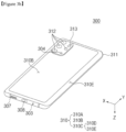
- FIG. 3B is a rear perspective view of the electronic device according to an embodiment.
- FIG. 3C is an exploded perspective view of the electronic device according to an embodiment.
- the electronic device 300 may include a housing 310 that includes a first surface (or, a front surface) 310A, a second surface (or, a rear surface) 310B, and a side surface 310C surrounding a space between the first surface 310A and the second surface 310B.
- the housing 310 may refer to a structure that forms some of the first surface 310A, the second surface 310B, and the side surface 310C of FIG. 1 .
- the first surface 310A may be formed by a front plate 302, at least a portion of which is substantially transparent (e.g., a glass plate including various coating layers, or a polymer plate).
- the second surface 310B may be formed by a back plate 311 that is substantially opaque.
- the back plate 311 may be formed of, for example, coated or colored glass, ceramic, a polymer, metal (e.g., aluminum, stainless steel (STS), or magnesium), or a combination of at least two of the aforementioned materials.
- the side surface 310C may be formed by a side bezel structure (or, a "frame structure") 318 that is coupled with the front plate 302 and the back plate 311 and that includes metal and/or a polymer.
- the back plate 311 and the side bezel structure 318 may be integrally formed with each other and may include the same material (e.g., a metallic material such as aluminum).
- the front plate 302 may include, at opposite long edges thereof, two first regions 310D that curvedly and seamlessly extend from the first surface 310A toward the back plate 311.
- the back plate 311 may include, at opposite long edges thereof, two second regions 310E that curvedly and seamlessly extend from the second surface 310B toward the front plate 302.
- the front plate 302 may include only one of the first regions 310D (or, the second regions 310E). In another embodiment, the front plate 302 (or, the back plate 311) may not include a part of the first regions 310D (or, the second regions 310E).
- the side bezel structure 318 when viewed from a side of the electronic device 300, may have a first thickness (or, width) at sides (e.g., short sides) not including the first regions 310D or the second regions 310E and may have a second thickness at sides (e.g., long sides) including the first regions 310D or the second regions 310E, the second thickness being smaller than the first thickness.
- the electronic device 300 may include at least one of a display 301, an audio module 303, 304, and 307 (e.g., the audio module 170 of FIG. 1 ), a sensor module (not illustrated) (e.g., the sensor module 176 of FIG. 1 ), camera modules 305 and 312 (e.g., the camera module 180 of FIG. 1 ), key input devices 317 (e.g., the input device 150 of FIG. 1 ), a light emitting element (not illustrated), or a connector hole 308 (e.g., the connecting terminal 178 of FIG. 1 ).
- the electronic device 300 may not include at least one component (e.g., the key input devices 317) among the aforementioned components, or may additionally include other component(s) (e.g., a light emitting element (not illustrated)).
- the display 301 may be exposed through most of the front plate 302. In some embodiments, at least a portion of the display 301 may be exposed through the front plate 302 that includes the first surface 310A and the first regions 310D of the side surface 310C.
- the periphery of the display 301 may be formed to be substantially the same as the shape of the adjacent outside edge of the front plate 302.
- the gap between the periphery of the display 301 and the periphery of the front plate 302 may be formed to be substantially constant.
- a surface of the housing 310 may include a screen display region that is formed as the display 301 is visually exposed.
- the screen display region may include the first surface 310A and the first regions 310D of the side surface.
- the screen display region 310A and 310D may include a sensing region (not illustrated) that is configured to obtain biometric information of a user.
- a sensing region (not illustrated) that is configured to obtain biometric information of a user.
- the sensing region may refer to a region capable of displaying visual information by the display 301 like the other regions of the screen display region 310A and 310D and additionally obtaining the user's biometric information (e.g., fingerprint).
- the screen display region 310A and 310D of the display 301 may include a region through which the first camera module 305 (e.g., a punch hole camera) is visually exposed. For example, at least a portion of the periphery of the region through which the first camera module 305 is exposed may be surrounded by the screen display region 310A and 310D.
- the first camera module 305 may include a plurality of camera modules (e.g., the camera module 180 of FIG. 1 ).
- the display 301 may include, on a rear surface of the screen display region 310A and 310D, at least one of the audio module 303, 304, and 307, a sensor module (e.g., the sensor module 176 of FIG. 1 ), a camera module (e.g., the first camera module 305), or a light emitting element (not illustrated).
- a sensor module e.g., the sensor module 176 of FIG. 1
- a camera module e.g., the first camera module 305
- a light emitting element not illustrated.
- the camera module (e.g., the first camera module 305) may be disposed on a rear side (e.g., a side facing the -Z-axis direction) of the first surface 310A (e.g., the front surface) and/or the side surface 310C (e.g., at least one of the first regions 310D) so as to face toward the first surface 310A and/or the side surface 310C.
- the first camera module 305 may include an under display camera (UDC) that is hidden without being visually exposed on the screen display region.
- UDC under display camera
- the display 301 may be coupled with, or disposed adjacent to, touch detection circuitry, a pressure sensor capable of measuring the intensity (pressure) of a touch, and/or a digitizer for detecting a stylus pen of a magnetic type.
- the audio module 303, 304, and 307 may include the microphone holes 303 and 304 and the speaker hole 307.
- a microphone for obtaining an external sound may be disposed in the microphone hole 303.
- the microphone may include a plurality of microphones to detect the direction of a sound.
- the microphone hole 304 formed in a partial region of the second surface 310B may be disposed adjacent to the camera modules 305 and 312. For example, the microphone hole 304 may obtain a sound when the camera modules 305 and 312 are executed, or may obtain a sound when another function is executed.
- the speaker hole 307 may include an external speaker hole 307 and a receiver hole for telephone call (not illustrated).
- the speaker hole 307 and the microphone hole 303 may be implemented as a single hole.
- the electronic device 300 may include a speaker fluidly connected with the speaker hole 307.
- the speaker may include a piezoelectric speaker from which the speaker hole 307 is omitted.
- the sensor module (not illustrated) (e.g., the sensor module 176 of FIG. 1 ) may generate an electrical signal or a data value that corresponds to an operational state inside the electronic device 300 or an environmental state external to the electronic device 300.
- the sensor module (not illustrated) may be disposed on the first surface 310A and/or the second surface 310B of the housing 310.
- the sensor module may include at least one of a proximity sensor, an HRM sensor, a fingerprint sensor, a gesture sensor, a gyro sensor, an atmospheric pressure sensor, a magnetic sensor, an acceleration sensor, a grip sensor, a color sensor, an infrared (IR) sensor, a biosensor, a temperature sensor, a humidity sensor, or an illuminance sensor.
- a proximity sensor e.g., an HRM sensor, a fingerprint sensor, a gesture sensor, a gyro sensor, an atmospheric pressure sensor, a magnetic sensor, an acceleration sensor, a grip sensor, a color sensor, an infrared (IR) sensor, a biosensor, a temperature sensor, a humidity sensor, or an illuminance sensor.
- IR infrared
- the camera modules 305 and 312 may include the first camera module 305 (e.g., a punch hole camera) exposed on the first surface 310A of the electronic device 300, the second camera module 312 exposed on the second surface 310B of the electronic device 300, and/or a flash 313.
- first camera module 305 e.g., a punch hole camera
- second camera module 312 exposed on the second surface 310B of the electronic device 300
- flash 313 e.g., a flash 313.
- the first camera module 305 may be exposed through a portion of the screen display region 310A and 310D of the display 301.
- the first camera module 305 may be exposed on a partial region of the screen display region 310A and 310D through an opening (not illustrated) that is formed in a portion of the display 301.
- the second camera module 312 may include a plurality of camera modules (e.g., a dual camera or a triple camera). However, the second camera module 312 is not necessarily limited to including the plurality of camera modules and may include one camera module.
- the first camera module 305 and the second camera module 312 may include one or more lenses, an image sensor, and/or an image signal processor.
- the flash 313 may include, for example, a light emitting diode or a xenon lamp.
- two or more lenses (an IR camera lens, a wide angle lens, and a telephoto lens) and image sensors may be disposed on one surface of the electronic device 300.
- the key input devices 317 may be disposed on the side surface 310C (e.g., the first regions 310D and/or the second regions 310E) of the housing 310.
- the electronic device 300 may not include all or some of the aforementioned key input devices 317, and the key input devices 317 not included may be implemented in a different form, such as a soft key, on the display 301.
- the key input devices may include a sensor module (not illustrated) that forms the sensing region (not illustrated) that is included in the screen display region 310A and 310D.
- the connector hole 308 may accommodate a connector. In an embodiment, the connector hole 308 may be disposed in the side surface 310C of the housing 310.
- the electronic device 300 may include the first connector hole 308 capable of accommodating a connector (e.g., a USB connector) for transmitting and receiving power and/or data with an external electronic device, and/or a second connector hole (not illustrated) capable of accommodating a connector (e.g., an earphone jack) for transmitting and receiving audio signals with an external electronic device.
- the electronic device 300 may include a light emitting element (not illustrated).
- the light emitting element may be disposed on the first surface 310A of the housing 310.
- the light emitting element may provide state information of the electronic device 300 in the form of light.
- the light emitting element may provide a light source operating in conjunction with the first camera module 305.
- the light emitting element may include an LED, an IR LED, and/or a xenon lamp.
- the electronic device 300 may include a front plate 320 (e.g., the front surface 310A and the first regions 310D of FIG. 3A ), a display 330 (e.g., the display 301 of FIG. 3A ), a bracket 340, a battery 349, a printed circuit board 350 (e.g., a printed circuit board (PCB), a flexible PCB (FPCB), or a rigid-flexible PCB (RFPCB)), a support member 360 (e.g., a rear case), and a back plate 380 (e.g., the rear surface 310B and the second regions 310E of FIG. 3A ).
- a front plate 320 e.g., the front surface 310A and the first regions 310D of FIG. 3A
- a display 330 e.g., the display 301 of FIG. 3A
- a bracket 340 e.g., the battery 349
- a printed circuit board 350 e.g., a
- the electronic device 300 may not include at least one component (e.g., the support member 360) among the aforementioned components, or may additionally include other component(s). At least one of the components of the electronic device 300 may be the same as, or similar to, at least one of the components of the electronic device 300 of FIGS. 3A and 3B , and repetitive descriptions will hereinafter be omitted.
- the front plate 320, the back plate 380, and at least a portion of the bracket 340 may form the housing (e.g., the housing 310 of FIGS. 3A and 3B ).
- the bracket 340 may include the frame structure 341 that forms a surface of the electronic device 300 (e.g., a portion of the side surface 310C of FIG. 1 ) and a plate structure 342 extending from the frame structure 341 into the electronic device 300.
- the plate structure 342 may be located inside the electronic device 300 and may be connected with the frame structure 341, or may be integrally formed with the frame structure 341.
- the plate structure 342 may be formed of, for example, a metallic material and/or a nonmetallic (e.g., polymer) material.
- the display 330 may be coupled to one surface of the plate structure 342, and the printed circuit board 350 may be coupled to an opposite surface of the plate structure 142.
- the printed circuit board 350 may have a processor, a memory, and/or an interface mounted thereon.
- the processor may include, for example, one or more of a central processing unit, an application processor, a graphic processing unit, an image signal processor, a sensor hub processor, or a communication processor.
- the memory may include, for example, a volatile memory or a nonvolatile memory.
- the interface may include, for example, a high definition multimedia interface (HDMI), a universal serial bus (USB) interface, an SD card interface, and/or an audio interface.
- HDMI high definition multimedia interface
- USB universal serial bus
- the interface may electrically or physically connect the electronic device 300 with an external electronic device and may include a USB connector, an SD card/MMC connector, or an audio connector.
- the battery 349 may supply power to at least one of the components of the electronic device 300.
- the battery 349 may include a primary cell that is not rechargeable, a secondary cell that is rechargeable, or a fuel cell.
- at least a portion of the battery 349 may be disposed on substantially the same plane as the printed circuit board 350.
- the battery 349 may be integrally disposed inside the electronic device 300, or may be disposed so as to be detachable from the electronic device 300.
- the first camera module 305 may be disposed on the plate structure 342 of the bracket 340 such that a lens is visually exposed through a partial region of the front plate 320 (e.g., the front surface 310A of FIG. 1 ) of the electronic device 300.
- the first camera module 305 may be disposed such that the optical axis of the lens is at least partially aligned with a hole or recess 337 formed in the display 330.
- the region through which the lens is exposed may be formed in the front plate 320.
- the first camera module 305 may include a punch hole camera, at least a portion of which is disposed in the hole or recess 337 formed in a rear surface of the display 330.
- the second camera module 312 may be disposed on the printed circuit board 350 such that a lens is exposed through a camera region 384 of the back plate 380 (e.g., the rear surface 310B of FIG. 2 ) of the electronic device 300.
- the second camera module 312 may be disposed in at least a portion of an inner space (e.g., a space formed by the plate structure 342) that is formed in the housing 310 of the electronic device 300 and may be electrically connected to the printed circuit board 350 through a connection member (e.g., a connector (e.g., a connector 423 of FIG. 4 )).
- the camera region 384 may be formed in a surface (e.g., the rear surface 310B of FIG. 2 ) of the back plate 380. In an embodiment, the camera region 384 may be formed to be at least partially transparent such that external light is incident on the lens of the second camera module 312. In an embodiment, at least a portion of the camera region 384 may protrude to a predetermined height from the surface of the back plate 380. However, without being necessarily limited thereto, the camera region 384 may form substantially the same plane as the surface of the back plate 380.
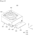
- FIG. 4 is a view illustrating a camera module of the electronic device according to an embodiment.
- the camera module 400 may include a fixed part 401 fixedly disposed in the electronic device (e.g., the electronic device 300 of FIGS. 3A to 3C ) and a moving part 402, at least a portion of which is disposed in the fixed part 401.
- the fixed part 401 may include a first circuit board 420.
- the moving part 402 may include a lens 405 (e.g., the lens assembly 210 of FIG. 2 ).
- the lens 405 included in the moving part 402 may be at least partially exposed outside the fixed part 401 through an opening formed in the fixed part 401.
- the lens 405 may be visible through the opening.
- the moving part 402 may be configured such that the lens 405 receives light external to the electronic device through a partial region (e.g., the camera region 384 of FIG. 3C ) of a surface (e.g., the back plate 380 of FIG. 3C ) of the housing of the electronic device (e.g., the electronic device 300 of FIG. 3 ).
- the region through which the lens 405 is exposed may include a transparent region of the housing of the electronic device.
- the moving part 402 may further include an image sensor (e.g., the image sensor 230 of FIG. 2 ) configured to convert a light signal received through the lens 405 into an electrical signal.
- the fixed part 401 may include the first circuit board 420.
- the first circuit board 420 may include a second region 422 extending outward from the inside of the fixed part 401 and the connector 423 disposed on the second region 422.
- the connector 423 may be coupled to the printed circuit board (e.g., the printed circuit board 350 of FIG. 3C ) of the electronic device (e.g., the electronic device 300 of FIGS. 3A to 3C ).
- an electrical signal generated by the image sensor of the moving part 402 e.g., the image sensor 230 of FIG. 2 or an image sensor 442 of FIG.
- the fixed part 401 may be formed in the form of a camera housing 403 in which the moving part 402 is accommodated.
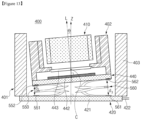
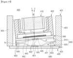
- FIG. 5 is a view illustrating a tilt operation of the camera module of the electronic device according to an embodiment.
- the camera module 400 may include the fixed part 401, the moving part 402, and a connecting structure (not illustrated).
- the fixed part 401 may include the camera housing 403 and the first circuit board 420, at least a portion of which is disposed in the camera housing 403.
- the first circuit board 420 may include a first region 421 disposed in the camera housing 403, the second region 422 flexibly extending outside the camera housing 403 from the first region 421, and the connector 423 disposed on the second region 422.
- the moving part 402 may include the lens 405, the image sensor (e.g., the image sensor 230 of FIG. 2 or the image sensor 442 of FIG. 6A ), and a second circuit board 440 electrically connected with the image sensor 442.
- the image sensor 442 may be configured to convert a light signal received from the lens 405 into an electrical signal.
- the image sensor 442 may be disposed on the second circuit board 440, or may be electrically connected to the second circuit board 440 through a wire.
- the second circuit board 440 may be disposed to face the first region 421 of the first circuit board 420.
- the second circuit board 440 may be disposed such that the image sensor 442 is aligned with an optical axis L of the lens 405.
- the moving part 402 may be coupled to the fixed part 401 so as to be rotatable.
- the moving part 402 may be configured to rotate about the center of rotation C.
- the center of rotation C may be located inside the moving part 402, or may be located between the moving part 402 and the fixed part 401.
- the center of rotation C may be a point through which the optical axis L of the lens 405 passes.
- the optical axis L may be defined as a straight line connecting the center of symmetry of a refractive surface or a reflective surface of the lens 405.
- the optical axis L may be a central axis of rotation in the spherical or aspheric (e.g., parabolic or hyperbolic) lens 405.
- the moving part 402 may be configured to rotate about at least one rotational axis R1, R2, and R3 perpendicular to the optical axis L of the lens 405. In an embodiment, the moving part 402 may be configured to rotate about at least one rotational axis R1, R2, and R3 parallel to the optical axis L of the lens 405.
- the first rotational axis R1 and the second rotational axis R2 substantially perpendicular to the optical axis L of the lens 405 may be defined.
- the first rotational axis R1 and the second rotational axis R2 may be substantially perpendicular to each other.
- the center of rotation C may be a point at which the rotational axes substantially intersect one another.
- the lens 405 may be moved (e.g., in the Z/-Z-axis direction) with respect to the optical axis L of the lens 405 in a space formed in the camera housing 403.
- the lens 405 may linearly move in the direction of the optical axis L together with a structure (e.g., a lens carrier or a lens assembly (e.g., the lens assembly 210 of FIG. 2 )) included in the moving part 402.
- the camera module 400 may provide an auto focus (AF) function by moving the lens 405 in a direction (e.g., the Z/-Z-axis direction) substantially parallel to the optical axis L of the lens 405.
- AF auto focus
- the camera module 400 may include an actuator (not illustrated) (e.g., a coil and/or a magnet) related to the auto focus function and may perform the auto focus function using the actuator.
- an actuator e.g., a coil and/or a magnet
- the camera module 400 may control an electromagnetic force by controlling a current (e.g., intensity and direction) flowing through the coil and may move a lens carrier 410 in a direction substantially parallel to the optical axis L by using the Lorentz force by the electromagnetic force.
- the moving part 402 may be configured to be rotatable about the first rotational axis R1 and/or the second rotational axis R2.
- the moving part 402 may rotate relative to the fixed part 401.
- the camera module 400 may perform an image stabilization function (e.g., an OIS function).
- the camera module 400 may perform a shake compensation function (e.g., an image stabilization function) by rotating the moving part 402 about the first rotational axis R1 and/or the second rotational axis R2.
- the camera module 400 may include an actuator (not illustrated) (e.g., a coil and/or a magnet) related to the image stabilization function and may perform the image stabilization function using the actuator.
- the camera module 400 may control an electromagnetic force by controlling a current (e.g., intensity and direction) flowing through the coil and may rotate the moving part 402 about the first rotational axis R1 and/or the second rotational axis R2 by using the Lorentz force by the electromagnetic force.
- a current e.g., intensity and direction
- the moving part 402 may rotate about the first rotational axis R1 and/or the second rotational axis R2 such that the optical axis L of the lens 405 has a predetermined range (e.g., movement range) with respect to the Z-axis.
- the camera module 400 may include a guide member (not illustrated) (e.g., a guide plate) related to a movement range of the moving part 402.
- a 3-axis rotary motion related to a movement of the moving part 402 may include a rolling motion, a pitching motion, or a yawing motion.
- a motion related to the first rotational axis R1 may be defined as a rolling motion
- a motion related to the second rotational axis R2 may be defined as a pitching motion.
- a motion related to the third rotational axis R3 may be defined as a yawing motion.
- the third rotational axis R3 may be an axis orthogonal to an orthogonal plane of the rolling motion and the pitching motion.
- the third rotational axis R3 may substantially coincide with the optical axis L of the lens 405.
- a connecting structure may electrically and/or physically connect the second circuit board 440 included in the moving part 402 and the first circuit board 420 included in the fixed part 401.
- the connecting structure may be physically coupled to the first circuit board 420 and the second circuit board 440 to electrically connect the first circuit board 420 and the second circuit board 440.
- the connecting structure of the camera module 400 may be configured to maintain the physical coupling and/or electrical connection between the fixed part 401 and the moving part 402 when the moving part 402 of the camera module 400 moves relative to the fixed part 401.
- the connecting structure may electrically connect the first circuit board 420 and the second circuit board 440 without affecting a movement (e.g., rotation) of the moving part 402.
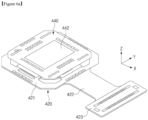
- FIG. 6A is a view illustrating the first circuit board and the second circuit board of the camera module of the electronic device according to an embodiment.
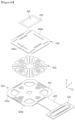
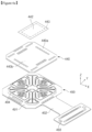
- FIG. 6B is an exploded perspective view illustrating the first circuit board, the second circuit board, and the connecting structure of the electronic device according to an embodiment.
- the camera module 400 may include the first circuit board 420, the second circuit board 440, and the connecting structure 500.
- the second circuit board 440 may be included in the moving part of the camera module 400 (e.g., the moving part 402 of FIG. 5 ).
- the second circuit board 440 may include a third surface 440a facing the Z-axis direction and a fourth surface 440b facing away from the third surface 440a.
- the third surface 440a and the fourth surface 440b of the second circuit board 440 may be defined as surfaces facing the direction of the optical axis L of the lens (e.g., the lens 405 of FIG. 5 ).
- the second circuit board 440 may be configured to rotate together with the moving part 402 when the electronic device (e.g., the electronic device 300 of FIGS. 3A to 3C ) performs an image stabilization function.
- the second circuit board 440 may be electrically connected with the image sensor 442.
- the image sensor 442 may be disposed on the third surface 440a of the second circuit board 440.
- the image sensor 442 may be surface-mounted on the second circuit board 440.
- the image sensor 442 according to an embodiment is not limited to being disposed on the third surface 440a of the second circuit board 440.
- the image sensor 442 may be disposed in an opening region (not illustrated) that is formed in the second circuit board 440 and may be electrically connected to the first circuit board 420 through a connecting member (e.g., wire bonding).
- the second circuit board 440 may further include an infrared filter 443 that overlaps at least a portion of the image sensor 442 when viewed in the Z-axis direction.
- the infrared filter 443 may have an area greater than or substantially the same as the area of the image sensor 442.
- the first circuit board 420 may be included in the fixed part of the camera module 400 (e.g., the fixed part 401 of FIG. 5 ).
- the first circuit board 420 may include a first surface 420a facing the Z-axis direction and a second surface 420b facing away from the first surface 420a (e.g., a surface facing the -Z-axis direction).
- the first circuit board 420 may include the first region 421 at least partially facing the second circuit board 440, the second region 422 extending from the first region 421, and the connector 423 disposed on the second region 422.
- the connector 423 may be coupled to the printed circuit board (e.g., the printed circuit board 350 of FIG. 3C ) included in the electronic device (e.g., the electronic device 300 of FIGS. 3A to 3C ).
- the first circuit board 420 may be spaced apart from the second circuit board 440 by a predetermined gap.
- the first surface 420a of the first circuit board 420 may be spaced apart from the fourth surface 440b of the second circuit board 440 by the predetermined gap while facing the fourth surface 440b of the second circuit board 440.
- the first circuit board 420 may be disposed such that the first region 421 at least partially faces the fourth surface 440b of the second circuit board 440.
- the first circuit board 420 may be formed to be flexible.
- the first region 421 may be formed to be rigid, and the second region 422 may be formed to be flexible.
- the first circuit board 420 may be electrically connected with the second circuit board 440 through the connecting structure 500.
- the connecting structure 500 may be disposed in a space between the first surface 420a of the first circuit board 420 and the fourth surface 440b of the second circuit board 440. In an embodiment, the connecting structure 500 may extend from the first surface 420a of the first circuit board 420 to the fourth surface 440b of the second circuit board 440. In an embodiment, the connecting structure 500 may provide electrical connection between the first circuit board 420 and the second circuit board 440. For example, an electrical signal generated by the image sensor 442 may be transmitted to the first circuit board 420 through the second circuit board 440 and/or the connecting structure 500. The electrical signal may be transmitted to the processor of the electronic device (e.g., the processor 120 of FIG. 1 ) through the connector 423 of the first circuit board 420. In an embodiment, the connecting structure 500 may include at least one flexible substrate, at least a portion of which is formed to be flexible.
- FIG. 6C is a view illustrating a first circuit board 490 and a second circuit board 440 of the electronic device according to another embodiment.
- the first circuit board 490 illustrated in FIG. 6C may be understood as the first circuit board 420 and the connecting structure 500 of FIG. 6B that are integrally connected with each other.
- repetitive descriptions identical to ones given with reference to FIGS. 6A and 6B will be omitted.
- the first circuit board 490 may include a first region 491, a second region 492, a connecting region 494, and a connector 493.
- the first region 491 may at least partially face a fourth surface 440b of the second circuit board 440.
- the second region 492 may extend from the first region 491 to one side.
- the second region 492 may extend toward the printed circuit board (e.g., the printed circuit board 350 of FIG. 3C ) disposed in the electronic device (e.g., the electronic device 300 of FIG. 3C ).
- the connector 493 may be disposed on the second region 492.
- the connector 493 may be coupled to a corresponding connector of the printed circuit board 350 of the electronic device 300.
- the connecting region 494 may extend from the first region 491 and may be electrically and physically coupled with the second circuit board 440.
- the connecting region 494 may be formed to be flexible.
- the connecting region 494 may electrically connect the second circuit board 440 and the first region 491 of the first circuit board 490.
- the first circuit board 490 may be formed to be partially flexible.
- the first region 491 of the first circuit board 490 may be formed to be rigid, and the second region 492 and the connecting region 494 of the first circuit board 490 may be formed to be flexible.
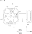
- FIG. 7 is a view illustrating the first circuit board of the camera module of the electronic device according to an embodiment.
- the first circuit board 420 may include at least one first conductive region 425.
- the first conductive region 425 may be formed on the first surface 420a of the first region 421 of the first circuit board 420.
- the first conductive region 425 may include a conductive region 1-1 425-1, a conductive region 1-2 425-2, a conductive region 1-3 425-3, and a conductive region 1-4 425-4.
- the first circuit board 420 is not limited to including four first conductive regions 425 and may include a plurality of (e.g., two, three, or five) first conductive regions 425.
- the first conductive region 425 may be formed in a position spaced apart from a first center point C1 of the first circuit board 420 by a first distance r1 in a radial direction.
- the first center point C1 of the first circuit board 420 may be defined as a geometric center of the first region 421 of the first circuit board 420.
- the first center point C1 may be defined as the center of the first region 421 in the X-axis direction and the Y-axis direction.
- the first center point C1 may be a point through which a virtual line extending from the optical axis of the lens (e.g., the optical axis L of FIG. 5 ) passes in a state (e.g., a default state) in which the moving part 402 is not rotated.
- the first conductive regions 425-1, 425-2, 425-3, and 425-4 may have substantially the same radius when viewed based on a virtual circle having the first center point C1 as the center.
- the conductive region 1-1 425-1 may be located in the +Y-axis direction with respect to the first center point C1.
- the conductive region 1-2 425-2 may be located in the +X-axis direction with respect to the first center point C1.
- the conductive region 1-3 425-3 may be located in the -Y-axis direction with respect to the first center point C1.
- the conductive region 1-4 425-4 may be located in the -X-axis direction with respect to the first center point C1.
- the first conductive regions 425-1, 425-2, 425-3, and 425-4 may be disposed at the same intervals.
- one of the first conductive regions 425-1, 425-2, 425-3, and 425-4 may be spaced apart from another first conductive region adjacent thereto at substantially the same angle.
- one of the first conductive regions 425-1, 425-2, 425-3, and 425-4 may be spaced apart from another first conductive region adjacent thereto at a first angle (e.g., about 90 degrees).
- a first angle e.g., about 90 degrees
- the angle between the first conductive regions 425-1, 425-2, 425-3, and 425-4 may vary depending on the number of first conductive regions and is not limited to the first angle (e.g., 90 degrees).
- the first conductive regions 425-1, 425-2, 425-3, and 425-4 may have point symmetry with respect to the first center point C1.
- the conductive region 1-1 425-1 and the conductive region 1-3 425-3 may be symmetrical to each other with respect to an axis X1 that passes through the first center point C1 and is parallel to the X-axis.
- the conductive region 1-2 425-2 and the conductive region 1-4 425-4 may be symmetrical to each other with respect to an axis Y1 that passes through the first center point C1 and is parallel to the Y-axis.
- an edge region in which the first conductive regions 425-1, 425-2, 425-3, and 425-4 are formed may be defined in the first region 421 of the first circuit board 420.
- the edge region may be at least partially aligned with an edge region of the second circuit board 440, which will be described below, in the Z-axis direction or the direction of the optical axis (e.g., the optical axis L of FIG. 5 ) of the lens (e.g., the lens 405 of FIG. 5 ).
- the positions and/or sizes of the first conductive regions 425-1, 425-2, 425-3, and 425-4 may be formed in various forms.
- the first conductive regions 425-1, 425-2, 425-3, and 425-4 may be formed in various forms depending on the shape of the flexible substrate of the connecting structure (e.g., the connecting structure 500 of FIG. 5 ).
- the connecting structure e.g., the connecting structure 500 of FIG. 5
- the first circuit board 420 may include first conductive regions corresponding to the position and/or size of the first conductive pad.
- FIG. 8 is a view illustrating the second circuit board of the camera module of the electronic device according to an embodiment.
- the image sensor 442 may be disposed on the third surface 440a of the second circuit board 440.
- At least one second conductive region 445 may be formed on the fourth surface 440b of the second circuit board 440.
- the fourth surface 440b of the second circuit board 440 may at least partially face the first region (e.g., the first region 421 of FIG. 7 ) of the first circuit board (e.g., the first circuit board 420 of FIG. 7 ).
- the image sensor 442 may be disposed to overlap a second center point C2.
- the second center point C2 of the second circuit board 440 may be a geometric center of the second circuit board 440.
- the second center point C2 may be defined as the center of the second circuit board 440 in the X-axis direction and the Y-axis direction.
- the second center point C2 may be a point through which a virtual line extending from the optical axis of the lens (e.g., the optical axis L of FIG. 5 ) passes in a state (e.g., the default state) in which the moving part 402 is not rotated.
- the second conductive region 445 may be formed in a position spaced apart from the second center point C2 of the second circuit board 440 by a second distance r2 in a radial direction.
- second conductive regions 445-1, 445-2, 445-3, and 445-4 may have substantially the same radius when viewed based on a virtual circle having the second center point C2 as the center.
- the second conductive region 445 may include a conductive region 2-1 445-1, a conductive region 2-2 445-2, a conductive region 2-3 445-3, and a conductive region 2-4 445-4.
- the second circuit board 440 is not limited to including four second conductive regions and may include a plurality of (e.g., two, three, or five) second conductive regions 425.
- the conductive region 2-1 445-1 may be located in the +Y-axis direction with respect to the second center point C2.
- the conductive region 2-2 445-2 may be located in the +X-axis direction with respect to the second center point C2.
- the conductive region 2-3 445-3 may be located in the -Y-axis direction with respect to the second center point C2.
- the conductive region 2-4 425-4 may be located in the -X-axis direction with respect to the second center point C2.
- the second conductive regions 445-1, 445-2, 445-3, and 445-4 may be disposed at the same intervals.
- one of the second conductive regions 445-1, 445-2, 445-3, and 445-4 may be spaced apart from another second conductive region adjacent thereto at substantially the same angle.
- one of the second conductive regions 445-1, 445-2, 445-3, and 445-4 may be spaced apart from another second conductive region adjacent thereto at a second angle (e.g., 90 degrees).
- the angle between the second conductive regions 445-1, 445-2, 445-3, and 445-4 may vary depending on the number of second conductive regions 445 and is not limited to the second angle (e.g., 90 degrees).
- the second conductive region 445 of the second circuit board 440 may be electrically connected with the first conductive region (e.g., the first conductive region 425 of FIG. 7 ) of the first circuit board (e.g., the first circuit board 420 of FIG. 7 ).
- the conductive region 2-1 445-1 may be electrically connected with the conductive region 1-1 of the first circuit board 420 (e.g., the conductive region 1-1 425-1 of FIG. 7 ).
- the conductive region 2-2 445-2 may be electrically connected with the conductive region 1-2 of the first circuit board 420 (e.g., the conductive region 1-2 425-2 of FIG. 7 ).
- the conductive region 2-3 445-3 may be electrically connected with the conductive region 1-3 of the first circuit board 420 (e.g., the conductive region 1-3 425-3 of FIG. 7 ).
- the conductive region 2-4 445-4 may be electrically connected with the conductive region 1-4 of the first circuit board 420 (e.g., the conductive region 1-4 425-4 of FIG. 7 ).
- the positions and/or sizes of the second conductive regions 445-1, 445-2, 445-3, and 445-4 may be formed in various forms.
- the second conductive regions 445-1, 445-2, 445-3, and 445-4 may be formed in various forms depending on the shape of the flexible substrate of the connecting structure (e.g., the connecting structure 500 of FIG. 5 ).
- the connecting structure e.g., the connecting structure 500 of FIG. 5
- the second circuit board 440 may include second conductive regions corresponding to the position and/or size of the second conductive pad.
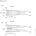
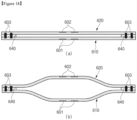
- FIG. 9 is a view illustrating the connecting structure of the camera module of the electronic device according to an embodiment.
- the connecting structure may include at least one flexible substrate 501.
- the flexible substrate 501 may include a first portion 510, a second portion 520, VIAs 531 and 532, and an adhesive layer (e.g., an adhesive layer 538 of FIG. 10 ) that couples the first portion 510 and the second portion 520.
- the first portion 510 and the second portion 520 may be physically coupled through the VIAs 531 and 532 and the adhesive layer.
- an adhesive material e.g., an optical clear adhesive (OCA) or a pressure sensitive adhesive (PSA)
- OCA optical clear adhesive
- PSA pressure sensitive adhesive
- the first portion 510 and the second portion 520 may be electrically connected through the VIAs 531 and 532.
- the VIAs 531 and 532 may be configured to electrically connect a first conductive pattern included in the first portion 510 and a second conductive pattern included in the second portion 520.
- the VIAs 531 and 532 may include the first VIA 531 located on one side of a first pad region 512 and a second pad region 522 (e.g., the left side based on the drawing) and the second VIA 532 located on an opposite side of the first pad region 512 and the second pad region 522 (e.g., the right side based on the drawing).
- the first portion 510 may include the first pad region 512 in which a first conductive pad 511 is formed, the first VIA regions 513 and 514 in which the VIAs 531 and 532 are formed, and first extension regions 515-1 and 515-2 extending from the first pad region 512 to the first VIA regions 513 and 514.
- the first VIA regions 513 and 514 may include the VIA region 1-1 513 in which the first VIA 531 is formed and the VIA region 1-2 514 in which the second VIA 532 is formed.
- the first pad region 512 may be located between the VIA region 1-1 513 and the VIA region 1-2 514.
- the first extension regions 515-1 and 515-2 may include the extension region 1-1 515-1 extending from the first pad region 512 in a direction (a direction 1) toward a center line A and the extension region 1-2 515-2 extending in a direction (a direction 2) away from the center line A.
- the extension region 1-1 515-1 may be connected with the first pad region 512.
- the extension region 1-2 515-2 may be connected with the VIA region 1-1 513 and the VIA region 1-2 514.
- the second portion 520 may include the second pad region 522 in which a second conductive pad 522 is formed, the second VIA regions 523 and 524 in which the VIAs 531 and 532 are formed, and second extension regions 525-1 and 525-2 extending from the second pad region 522 to the second VIA regions 523 and 524.
- the second VIA regions 523 and 524 may include the VIA region 2-1 523 in which the first VIA 531 is formed and the VIA region 2-2 524 in which the second VIA 532 is formed.
- the second pad region 522 may be located between the VIA region 2-1 523 and the VIA region 2-2 524.
- the second extension regions 525-1 and 525-2 may include the extension region 2-1 525-1 extending from the second pad region 522 in the direction (the direction 1) toward the center line A and the extension region 2-2 525-2 extending in the direction (the direction 2) away from the center line A.
- the extension region 2-1 525-1 may be connected with the second pad region 522.
- the extension region 2-2 525-2 may be connected with the VIA region 2-1 523 and the VIA region 2-2 524.
- first extension regions 515-1 and 515-2 and/or the second extension regions 525-1 and 525-2 are illustrated in a shape bent once.
- first extension regions 515-1 and 515-2 and/or the second extension regions 525-1 and 525-2 may be formed in a shape bent a plurality of times (e.g., three times).
- a plurality of first extension regions 515-1 and 515-2 and/or a plurality of second extension regions 525-1 and 525-2 may be sequentially disposed to electrically connect the first pad region 512 and/or the second pad region 522 with the first VIA regions 513 and 514 and/or the second VIA regions 523 and 524.
- the first extension regions 515-1 and 515-2 and/or the second extension regions 525-1 and 525-2 may have different lengths.
- the first extension regions 515-1 and 515-2 and/or the second extension regions 525-1 and 525-2 may have a gradually increasing length toward the first VIA regions 513 and 514 and/or the second VIA regions 523 and 524 in the first pad region 512 and/or the second pad region 522.
- the center line A may be defined on the flexible substrate 501.
- the center line A may be defined as a virtual line extending from the edge regions of the first circuit board 420 and the second circuit board 440 illustrated in FIGS. 7 and 8 toward the first center point C1 and the second center point C2.
- the center line A may pass through the first pad region 512 and the second pad region 522.
- the first pad region 512 may be formed in a symmetrical shape with respect to the center line A.
- the first pad region 512 may be spaced apart from the first VIA regions 513 and 514 by a predetermined gap.
- the first pad region 512 may be located between the VIA region 1-1 513 and the VIA region 1-2 514.
- the VIA region 1-1 513 and the VIA region 1-2 514 may have shapes substantially symmetrical to each other with respect to the center line A.
- the second pad region 522 may be formed in a symmetrical shape with respect to the center line A.
- the second pad region 522 may be spaced apart from the second VIA regions 523 and 524 by a predetermined gap.
- the second pad region 522 may be located between the VIA region 2-1 523 and the VIA region 2-2 524.
- the VIA region 2-1 523 and the VIA region 2-2 524 may have shapes substantially symmetrical to each other with respect to the center line A.
- first portion 510 and the second portion 520 may be configured such that the first pad region 512 and the second pad region 522 face each other, but are spaced apart from each other by a predetermined gap and the first VIA regions 513 and 514 and the second VIA regions 523 and 524 are coupled to each other.
- the gap between the first portion 510 and the second portion 520 may increase toward the pad regions 512 and 522 from the VIA regions 513, 514, 523, and 524.
- the first circuit board (e.g., the first circuit board 420 of FIG. 7 ) and the flexible substrate 501 may be formed of one circuit board.
- the first circuit board 490 may include an RFPCB that includes a rigid first region 491 and a flexible connecting region (e.g., the connecting region 494 of FIG. 6C ).
- the flexible substrate 501 may include the connecting region 494.
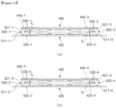
- FIG. 10 is a view illustrating the flexible substrate of the camera module of the electronic device according to an embodiment.
- FIG. 10 is a sectional view taken along the center line A illustrated in FIG. 9 .
- the flexible substrate 501 may include the adhesive layer 538.
- the adhesive layer 538 may be disposed between the first VIA regions 513 and 514 of the first portion 510 and the second VIA regions 523 and 524 of the second portion 520 of the flexible substrate 501 and may physically couple the first portion 510 and the second portion 520.
- the VIAs 531 and 532 may be formed through the first portion 510, the second portion 520, and the adhesive layer 538.
- the adhesive layer 538 may be formed by applying an adhesive material.
- the VIAs 531 and 532 may include a partial region of the first portion 510, a partial region of the second portion 520, a VIA hole penetrating the adhesive layer 538, and a conductive material filling at least a portion of the VIA hole.
- first pad region 512 and the second pad region 522 may face each other, but may be spaced apart from each other by a predetermined gap.
- the first VIA regions 513 and 514 and the second VIA regions 523 and 524 may be located between the first pad region 512 and the second pad region 522 when viewed based on the Z-axis.
- the first conductive pad 511 may be electrically connected with the first conductive region (e.g., the first conductive region 425 of FIG. 7 ) of the first circuit board (e.g., the first circuit board 420 of FIG. 7 ).
- the first conductive pad 511 may be surface-mounted or disposed on the first conductive region 425 of the first circuit board 420.
- the second conductive pad 521 may be electrically connected with the second conductive region (e.g., the second conductive region 445 of FIG. 8 ) of the second circuit board (e.g., the second circuit board 440 of FIG. 8 ).
- the second conductive pad 521 may be surface-mounted on the second conductive region 445 of the second circuit board 440.
- the VIAs 531 and 532 may electrically connect the first VIA regions 513 and 514 of the first portion 510 and the second VIA regions 523 and 524 of the second portion 520, and thus the first conductive region 425 of the first circuit board 420 and the second conductive region 445 of the second circuit board 440 may be electrically connected.
- FIG. 11A is a view illustrating the connecting structure 500 of the camera module of the electronic device according to an embodiment.
- FIG. 11B is a plan view of the first portion 510 of the connecting structure 500 of the camera module of the electronic device according to an embodiment.
- FIG. 11C is a plan view of the second portion 520 of the connecting structure 500 of the camera module of the electronic device according to an embodiment.
- the connecting structure 500 may be a structure including a plurality of flexible substrates 500-1, 500-2, 500-3, and 500-4. Each of the plurality of flexible substrates may be referred to as the flexible substrate 501 described with reference to FIGS. 9 and 10 .
- the connecting structure 500 may be configured to electrically and/or physically connect the first circuit board 420 and the second circuit board 440.
- the plurality of flexible substrates included in the connecting structure 500 may electrically connect the first conductive region 425 of the first circuit board 420 and the second conductive region 445 of the second circuit board 440.
- the connecting structure 500 may include the first flexible substrate 500-1, the second flexible substrate 500-2, the third flexible substrate 500-3, and the fourth flexible substrate 500-4.
- the number of flexible substrates included in the connecting structure 500 is not limited to that illustrated in the drawing, and the camera module 400 may include various numbers of flexible substrates.
- a third center point C3 that is a geometric center may be defined in the connecting structure 500.
- the third center point C3 may be the center of the connecting structure 500 in the X-axis direction and the Y-axis direction.
- the third point C3 may be located in a space surrounded by the first flexible substrate 500-1, the second flexible substrate 500-2, the third flexible substrate 500-3, and the fourth flexible substrate 500-4.
- the plurality of flexible substrates 500-1, 500-2, 500-3, and 500-4 may be symmetrically disposed with respect to the third center point C3.
- the first flexible substrate 500-1 and the third flexible substrate 500-3 may be formed in positions and/or shapes symmetrical to each other with respect to the axis X1 parallel to the direction of the X-axis passing through the third center point C3.
- the second flexible substrate 500-2 and the fourth flexible substrate 500-4 may be formed in positions and/or shapes symmetrical to each other with respect to the axis Y1 parallel to the direction of the Y-axis passing through the third center point C3.
- one flexible substrate among the plurality of flexible substrates 500-1, 500-2, 500-3, and 500-4 may be spaced apart from another flexible substrate adjacent thereto by a predetermined gap.
- the plurality of flexible substrates may be spaced apart from each other at a predetermined angle (e.g., about 90 degrees) when viewed with respect to the third center point C3.
- the plurality of flexible substrates 500-1, 500-2, 500-3, and 500-4 may be disposed such that conductive pads 511 and 521 included in the plurality of flexible substrates are located in a symmetric arrangement.
- conductive pads 511-1 and 521-1 of the first flexible substrate 500-1 may be formed in positions and/or shapes symmetrical to conductive pads 511-3 and 521-3 of the third flexible substrate 500-3 with respect to the axis X1.
- conductive pads 511-2 and 521-2 of the second flexible substrate 500-2 may be formed in positions and/or shapes symmetrical to conductive pads 511-4 and 521-4 of the fourth flexible substrate 500-4 with respect to the axis Y1.
- the first flexible substrate 500-1 may include a portion 1-1 510-1 and a portion 2-1 520-1.
- the portion 1-1 510-1 and the portion 2-1 520-1 may be coupled in regions around VIAs 531-1 and 532-1 (e.g., the VIA regions 513, 514, 523, and 524 of FIG. 9 ) and may be configured such that the conductive pad 1-1 511-1 and the conductive pad 2-1 521-1 are spaced apart from each other.
- the VIAs 531-1 and 532-1 may include the VIA 1-1 531-1 located on one side of the conductive pad 1-1 511-1 and the conductive pad 2-1 521-1 and the VIA 2-1 532-1 located on an opposite side of the conductive pad 1-1 511-1 and the conductive pad 2-1 521-1.
- the VIA 1-1 531-1 may be located in the counterclockwise direction of the conductive pad 1-1 511-1 and the conductive pad 2-1 521-1 with respect to the third center point C3
- the VIA 2-1 532-1 may be located in the clockwise direction of the conductive pad 1-1 511-1 and the conductive pad 2-1 521-1 with respect to the third center point C3.
- the second flexible substrate 500-2 may include a portion 1-2 510-2 and a portion 2-2 520-2.
- the portion 1-2 510-2 and the portion 2-2 520-2 may be coupled in regions around VIAs 531-2 and 532-2 (e.g., the VIA regions 513, 514, 523, and 524 of FIG. 9 ) and may be configured such that the conductive pad 1-2 511-2 and the conductive pad 2-2 521-2 are spaced apart from each other.
- the VIAs 531-2 and 532-2 may include the VIA 1-2 531-2 located on one side of the conductive pad 1-2 511-2 and the conductive pad 2-2 521-2 and the VIA 2-2 532-2 located on an opposite side of the conductive pad 1-2 511-2 and the conductive pad 2-2 521-2.
- the VIA 1-2 531-2 may be located in the counterclockwise direction of the conductive pad 1-2 511-2 and the conductive pad 2-2 521-2 with respect to the third center point C3
- the VIA 2-2 532-2 may be located in the clockwise direction of the conductive pad 1-2 511-2 and the conductive pad 2-2 521-2 with respect to the third center point C3.
- the third flexible substrate 500-3 may include a portion 1-3 510-3 and a portion 2-3 520-3.
- the portion 1-3 510-3 and the portion 2-3 520-3 may be coupled in regions around VIAs 531-3 and 532-3 (e.g., the VIA regions 513, 514, 523, and 524 of FIG. 9 ) and may be configured such that the conductive pad 1-3 511-3 and the conductive pad 2-3 521-3 are spaced apart from each other.
- the VIAs 531-3 and 532-3 may include the VIA 1-3 531-3 located on one side of the conductive pad 1-3 511-3 and the conductive pad 2-3 521-3 and the VIA 2-3 532-3 located on an opposite side of the conductive pad 1-3 511-3 and the conductive pad 2-3 521-3.
- the VIA 1-3 531-3 may be located in the counterclockwise direction of the conductive pad 1-3 511-3 and the conductive pad 2-3 521-3 with respect to the third center point C3, and the VIA 2-3 532-3 may be located in the clockwise direction of the conductive pad 1-3 511-3 and the conductive pad 2-3 521-3 with respect to the third center point C3.
- the fourth flexible substrate 500-4 may include a portion 1-4 510-4 and a portion 2-4 520-4.
- the portion 1-4 510-4 and the portion 2-4 520-4 may be coupled in regions around VIAs 531-4 and 532-4 (e.g., the VIA regions 513, 514, 523, and 524 of FIG. 9 ) and may be configured such that the conductive pad 1-4 511-4 and the conductive pad 2-4 521-4 are spaced apart from each other.
- the VIAs 531-4 and 532-4 may include the VIA 1-4 531-4 located on one side of the conductive pad 1-4 511-4 and the conductive pad 2-4 521-4 and the VIA 2-4 532-4 located on an opposite side of the conductive pad 1-4 511-4 and the conductive pad 2-4 521-4.
- the VIA 1-4 531-4 may be located in the counterclockwise direction of the conductive pad 1-4 511-4 and the conductive pad 2-4 521-4 with respect to the third center point C3
- the VIA 2-4 532-4 may be located in the clockwise direction of the conductive pad 1-4 511-4 and the conductive pad 2-4 521-4 with respect to the third center point C3.
- FIG. 12 is a view illustrating the connecting structure of the camera module of the electronic device according to an embodiment.
- (a) of FIG. 12 is a sectional view taken along line A-A' of FIG. 11
- (b) of FIG. 12 is a sectional view taken along line B-B' of FIG. 11 .
- the first flexible substrate 500-1 may electrically connect the conductive region 1-1 425-1 of the first circuit board 420 and the conductive region 2-1 445-1 of the second circuit board 440.
- the first conductive pad 511-1 of the first flexible substrate 500-1 may be electrically connected with the conductive region 1-1 425-1 of the first circuit board 420.
- the second conductive pad 521-1 of the first flexible substrate 500-1 may be electrically connected with the conductive region 2-1 445-1 of the second circuit board 440.
- the second flexible substrate 500-2 may electrically connect the conductive region 1-2 425-2 of the first circuit board 420 and the conductive region 2-2 445-2 of the second circuit board 440.
- the first conductive pad 511-2 of the second flexible substrate 500-2 may be electrically connected with the conductive region 1-2 425-2 of the first circuit board 420.
- the second conductive pad 521-2 of the second flexible substrate 500-2 may be electrically connected with the conductive region 2-2 445-2 of the second circuit board 440.
- the third flexible substrate 500-3 may electrically connect the conductive region 1-3 425-3 of the first circuit board 420 and the conductive region 2-3 445-3 of the second circuit board 440.
- the first conductive pad 511-3 of the third flexible substrate 500-3 may be electrically connected with the conductive region 1-3 425-3 of the first circuit board 420.
- the second conductive pad 521-3 of the third flexible substrate 500-3 may be electrically connected with the conductive region 2-3 445-3 of the second circuit board 440.
- the fourth flexible substrate 500-4 may electrically connect the conductive region 1-4 425-4 of the first circuit board 420 and the conductive region 2-4 445-4 of the second circuit board 440.
- the first conductive pad 511-4 of the fourth flexible substrate 500-4 may be electrically connected with the conductive region 1-4 425-4 of the first circuit board 420.
- the second conductive pad 521-4 of the fourth flexible substrate 500-4 may be electrically connected with the conductive region 2-4 445-4 of the second circuit board 440.
- the illustrated connecting structure 500 shows the default state in which the optical axis (e.g., the optical axis L of FIG. 5 ) of the lens (e.g., the lens 405 of FIG. 5 ) is substantially parallel to the Z-axis.
- the optical axis e.g., the optical axis L of FIG. 5
- the lens e.g., the lens 405 of FIG. 5
- the first conductive pad 511-1 and the second conductive pad 521-1 of the first flexible substrate 500-1 may form a first gap d1.
- the first conductive pad 511-2 and the second conductive pad 521-2 of the second flexible substrate 500-2 may form the first gap d1.
- the first conductive pad 511-3 and the second conductive pad 521-3 of the third flexible substrate 500-3 may form the first gap d1.
- the first conductive pad 511-4 and the second conductive pad 521-4 of the fourth flexible substrate 500-4 may form the first gap d1.
- FIG. 13 is a view illustrating a rotation operation of the camera module 400 of the electronic device according to an embodiment.
- FIG. 13 is a view illustrating the connecting structure when the moving part 402 rotates about a rotational axis (e.g., the first rotational axis R1 and the second rotational axis R2 of FIG. 5 ) perpendicular to the optical axis L.
- a rotational axis e.g., the first rotational axis R1 and the second rotational axis R2 of FIG. 5
- the moving part 402 may be accommodated in the inner space of the fixed part 401.
- the moving part 402 may be configured to rotate about the center of rotation C (e.g., the center of rotation C of FIG. 5 ) to perform an image stabilization function.
- the center of rotation C may be a point at which the optical axis L of the lens intersects a rotational axis (e.g., the rotational axes R1, R2, and R3 of FIG. 5 ).
- the center of rotation may be formed in the moving part 402.
- the center of rotation may be formed in the space between the moving part 402 and the fixed part 401.
- a lower surface of the moving part 402 may include the second circuit board 440.
- a lower surface of the fixed part 401 may include the first circuit board 420. At least a portion of the moving part 402 may be disposed in the fixed part 401 such that the first region 421 of the first circuit board 420 and the second circuit board 440 face each other.
- the moving part 402 may include the lens carrier 410 including the lens, the image sensor 442, and the infrared filter 443.
- the image sensor 442 may be disposed on the second circuit board 440.
- the moving part 402 may rotate relative to the fixed part 401 together with the lens carrier 410, the image sensor 442, the infrared filter 443, and the second circuit board 440.
- the moving part 402 may move (e.g., rotate) relative to the fixed part 401 by a predetermined angle ⁇ based on the Z-axis. In various embodiments, the predetermined angle ⁇ may be less than 10 degrees.
- the camera module 400 may include a plurality of flexible substrates 550 and 560 disposed in the space between the first circuit board 420 and the second circuit board 440 to electrically connect the first circuit board 420 and the second circuit board 440.
- the plurality of flexible substrate 550 and 560 may include the first flexible substrate 550 illustrated on the left side based on the drawing and the second flexible substrate 560 illustrated on the right side based on the drawing.
- the first flexible substrate 550 may be referred to as the first flexible substrate 500-1 and/or the third flexible substrate 500-3 illustrated in FIGS. 11 and 12 .
- the second flexible substrate 560 may be referred to as the second flexible substrate 500-2 and/or the fourth flexible substrate 500-4 illustrated in FIGS.
- first flexible substrate 550 and the second flexible substrate 560 illustrated in FIG. 13 may be referred to as one of the plurality of flexible substrates 500-1, 500-2, 500-3, and 500-4 illustrated in FIGS. 11 and 12 and another one thereof, respectively.
- first flexible substrate 550 and the second flexible substrate 560 may be flexible substrates disposed to be symmetrical to each other with the optical axis L or the Z-axis therebetween.
- the first flexible substrate 550 may include a first conductive pad 551 coupled to the first circuit board 420 and a second conductive pad 552 coupled to the second circuit board 440.
- the second flexible substrate 560 may include a third conductive pad 561 coupled to the first circuit board 420 and a fourth conductive pad 562 coupled to the second circuit board 440.
- the first conductive pad 551 and the third conductive pad 561 may be referred to as the first conductive pads 511-1, 511-2, 511-3, and 511-4 illustrated in FIGS. 11 and 12 .
- the second conductive pad 552 and the fourth conductive pad 562 may be referred to as the second conductive pads 521-1, 521-2, 521-3, and 521-4 illustrated in FIGS. 11 and 12 .
- the camera module 400 may include a first state (e.g., the default state) in which the optical axis L of the lens is parallel to the Z-axis and a second state (e.g., a rotated state) in which the optical axis L of the lens forms the predetermined angle ⁇ with the Z-axis.
- FIG. 13 illustrates the camera module 400 in the rotated state.
- the predetermined angle ⁇ may be less than 10 degrees.
- the first conductive pad 551 and the second conductive pad 552 of the first flexible substrate 550 may form a second gap d2.
- the third conductive pad 561 and the fourth conductive pad 562 of the second flexible substrate 560 may form a third gap d3 different from the second gap d2.
- the first circuit board 420 may be disposed to have a normal vector parallel to the Z-axis
- the second circuit board 440 may be disposed to have a normal vector parallel to the optical axis L.
- one of the second gap d2 and the third gap d3 may be greater than the first gap (e.g., the first gap d1 of FIG. 12 ), and the other one of the second gap d2 and the third gap d3 may be smaller than the first gap (e.g., the first gap d1 of FIG. 12 ).
- the plurality of flexible substrates 550 and 560 may be formed to be deformable depending on the gap between the first circuit board 420 and the second circuit board 440 and may electrically connect the first circuit board 420 and the second circuit board 440 even when the moving part 402 moves.
- the image sensor 442 may be disposed between the second circuit board 440 and the flexible substrate 560.
- a recess and/or hole (not illustrated) in which the image sensor 442 is disposed may be formed in at least a portion of the second circuit board 440, and the image sensor 442 may be disposed on at least a portion of the second circuit board 440.
- the image sensor 442 may obtain light incident on a space (e.g., a recess and/or hole) formed in at least a portion of the second circuit board 440 and may convert the incident light signal into an electrical signal.
- a camera module in the related art includes an FPCB that extends from a moving part to a printed circuit board (e.g., the printed circuit board 350 of FIG. 3 ) of an electronic device (e.g., the electronic device 300 of FIG. 3 ) located outside the camera module.
- a printed circuit board e.g., the printed circuit board 350 of FIG. 3
- an electronic device e.g., the electronic device 300 of FIG. 3
- One side of the FPCB may be coupled to the fixed printed circuit board 350, and therefore the tension of the FPCB may impede a movement of the moving part.
- the camera module in the related art includes an FPCB having an increased length.
- the FPCB is configured to be bent a plurality of times in various directions so as to be located in a limited inner space of the mobile electronic device 300.
- the connecting structure 500 of the camera module 400 may be disposed in the space between the second circuit board 440 of the moving part 402 and the first circuit board 420 of the fixed part 401 (e.g., in the camera housing 403), and thus the size of the camera module 400 may be decreased. This may be more useful in the mobile electronic device 300 having a limited inner space.
- the connecting structure 500 of the camera module 400 may be located in a relatively narrow range from the center of rotation C of the moving part and may have a relatively small length. Accordingly, when the moving part 402 moves, repulsive force acting on the moving part 402 may be reduced. In addition, when the moving part 402 moves, a movement range of the connecting structure 500 may be decreased. As a result, current consumption required to move the moving part 402 may be decreased, and thus efficiency may be increased.
- FIG. 14 is a view illustrating a connecting structure 600 of a camera module of the electronic device according to another embodiment.
- FIG. 15 is a view illustrating the connecting structure 600 of the camera module of the electronic device according to the other embodiment.
- the connecting structure 600 may include a first flexible substrate 610, a second flexible substrate 620, and a VIA 631.
- the VIA 631 formed in a VIA region 630 may be formed through one region of the first flexible substrate 610 and one region of the second flexible substrate 620.
- the VIA 631 may physically and/or electrically connect the first flexible substrate 610 and the second flexible substrate 620.
- the first flexible substrate 610 may be coupled to the first circuit board 420
- the second flexible substrate 620 may be coupled to the second circuit board 440.
- a fourth center point C4 may be defined in the first flexible substrate 610 and the second flexible substrate 620.
- the fourth center point C4 may be defined as a geometric center that is the center of the first flexible substrate 610 and the second flexible substrate 620 in the X-axis direction and the Y-axis direction.
- the first flexible substrate 610 and the second flexible substrate 620 may be disposed to face each other.
- the first flexible substrate 610 may include first conductive pads 611, 612, 613, and 614 and first extension regions 615-1 and 615-2 extending from the VIA region 630 to the first conductive pads 611, 612, 613, and 614.
- the first flexible substrate 610 may include the conductive pad 1-1 611, the conductive pad 1-2 612, the conductive pad 1-3 613, and the conductive pad 1-4 614.
- the first conductive pads 611, 612, 613, and 614 of the first flexible substrate 610 may be disposed at substantially the same distance from the fourth center point C4.
- the conductive pad 1-1 611 may be disposed in the Y-axis direction
- the conductive pad 1-2 612 may be disposed in the X-axis direction
- the conductive pad 1-3 613 may be disposed in the -Y-axis direction
- the conductive pad 1-4 614 may be disposed in the -X-axis direction.
- the conductive pad 1-1 611 and the conductive pad 1-3 613 may be disposed to be symmetrical to each other with respect to an axis X1 that is parallel to the X-axis and passes through the fourth center point C4.
- the conductive pad 1-2 612 and the conductive pad 1-4 614 may be disposed to be symmetrical to each other with respect to an axis Y1 that is parallel to the Y-axis and passes through the fourth center point C4.
- the conductive pad 1-1 611 may be coupled to the conductive region 1-1 425-1 of the first circuit board 420
- the conductive pad 1-2 612 may be coupled to the conductive region 1-2 425-2 of the first circuit board 420
- the conductive pad 1-3 613 may be coupled to the conductive region 1-3 425-3 of the first circuit board 420
- the conductive pad 1-4 614 may be coupled to the conductive region 1-4 425-4 of the first circuit board 420.
- the second flexible substrate 620 may include second conductive pads 621, 622, 623, and 624 and second extension regions 625-1 and 625-2 extending from the VIA region 630 to the second conductive pads 621, 622, 623, and 624.
- the second flexible substrate 620 may include the conductive pad 2-1 621, the conductive pad 2-2 622, the conductive pad 2-3 623, and the conductive pad 2-4 624.
- the second conductive pads 621, 622, 623, and 624 of the second flexible substrate 620 may be disposed at substantially the same distance from the fourth center point C4.
- the conductive pad 2-1 621 may be disposed in the Y-axis direction
- the conductive pad 2-2 622 may be disposed in the X-axis direction
- the conductive pad 2-3 623 may be disposed in the -Y-axis direction
- the conductive pad 2-4 624 may be disposed in the -X-axis direction.
- the conductive pad 2-1 621 and the conductive pad 2-3 623 may be disposed to be symmetrical to each other with respect to the axis X1 that is parallel to the X-axis and passes through the fourth center point C4.
- the conductive pad 2-2 622 and the conductive pad 2-4 624 may be disposed to be symmetrical to each other with respect to the axis Y1 that is parallel to the Y-axis and passes through the fourth center point C4.
- the conductive pad 2-1 621 may be coupled to the conductive region 2-1 445-1 of the second circuit board 440
- the conductive pad 2-2 622 may be coupled to the conductive region 2-2 445-2 of the second circuit board 440
- the conductive pad 2-3 623 may be coupled to the conductive region 2-3 445-3 of the second circuit board 440
- the conductive pad 2-4 624 may be coupled to the conductive region 2-4 445-4 of the second circuit board 440.
- the first conductive region 425 of the first circuit board 420 may be electrically connected with the second conductive region 445 of the second circuit board 440 through the first conductive pads 611, 612, 613, and 614, the VIA 631, and the second conductive pads 621, 622, 623, and 624 of the connecting structure 600.
- first flexible substrate 610 and the second flexible substrate 620 may be physically coupled in a region around the VIA 631 (e.g., the VIA region 630) and may be configured such that the first conductive pads 611, 612, 613, and 614 and the second conductive pads 621, 622, 623, and 624 are spaced apart from each other.
- conductive patterns connecting the VIA 631 and the first conductive pads 611, 612, 613, and 614 may be formed in the first extension regions 615-1 and 615-2.
- the first extension regions 615-1 and 615-2 may extend in a circumferential direction or a tangential direction.
- the first extension regions 615-1 and 615-2 may include the first region 615-1 extending in a first rotational direction (e.g., the clockwise direction) with respect to the fourth center point C4 and the second region 615-2 extending in a second rotational direction (e.g., the counterclockwise direction) opposite to the first rotational direction.
- the first extension regions 615-1 and 615-2 may be formed in a zigzag shape in which one or more first regions 615-1 and one or more second regions 615-2 are alternately disposed.
- the extension distances measured from the VIA region 630 to the first conductive pads 611, 612, 613, and 614 along the first extension regions 615-1 and 615-2 may be greater than the straight-line distances from the VIA region 630 to the first conductive pads 611, 612, 613, and 614.
- the first flexible substrate 610 may have a length to provide sufficient flexibility when the moving part 402 moves.
- conductive patterns connecting the VIA 631 and the second conductive pads 621, 622, 623, and 624 may be formed in the second extension regions 625-1 and 625-2.
- the second extension regions 625-1 and 625-2 may extend in the circumferential direction or the tangential direction.
- the second extension regions 625-1 and 625-2 may include the third region 625-1 extending in the first rotational direction (e.g., the clockwise direction) with respect to the fourth center point C4 and the fourth region 625-2 extending in the second rotational direction (e.g., the counterclockwise direction) opposite to the first rotational direction.
- the second extension regions 625-1 and 625-2 may be formed in a zigzag shape in which one or more third regions 625-1 and one or more fourth regions 625-2 are alternately disposed.
- the extension distances measured from the VIA region 630 to the second conductive pads 621, 622, 623, and 624 along the second extension regions 625-1 and 625-2 may be greater than the straight-line distances from the VIA region 630 to the second conductive pads 621, 622, 623, and 624.
- the second flexible substrate 620 may have a length to provide sufficient flexibility when the moving part 402 moves.
- the first flexible substrate 610 and the second flexible substrate 620 may be configured such that the gap increases from the VIA region 630, which is a central region, toward the conductive pads, which are edge regions.
- the first region 615-1 of the first extension regions 615-1 and 615-2 may be located closer to the fourth center point C4 than the second region 615-2.
- the third region 625-1 of the second extension regions 625-1 and 625-2 may be located closer to the fourth center point C4 than the fourth region 625-2.
- the gap between the first region 615-1 and the third region 625-1 may be smaller than the gap between the second region 615-2 and the fourth region 625-2.
- the shapes of the first extension regions 615-1 and 615-2 and the second extension regions 625-1 and 625-2 are not limited to the illustrated example and may be formed in various shapes.
- the first extension regions may have a shape bent a plurality of times (e.g., a zigzag shape).
- the first extension regions 615-1 and 615-2 may include a first region extending radially inward (e.g., in a direction toward the fourth center point C4) and a second region extending radially outward (e.g., in a direction away from the fourth center point C4).
- the second extension regions 625-1 and 625-2 may include a third region extending radially inward (e.g., in a direction toward the fourth center point C4) and a fourth region extending radially outward (e.g., in a direction away from the fourth center point C4).
- the first extension regions 615-1 and 615-2 or the second extension regions 625-1 and 625-2 may be asymmetrically formed with respect to the axes of symmetry X1 and Y1.
- the first extension regions 615-1 and 615-2 and the second extension regions 625-1 and 625-2 located on one side of the axes of symmetry X1 and Y1 may extend in zigzags in the tangential direction or the circumferential direction, and the first extension regions and the second extension regions located on an opposite side of the axes of symmetry X1 and Y1 may radially extend in zigzags.
- FIG. 16 is a view illustrating the connecting structure of the camera module of the electronic device according to the other embodiment.
- FIG. 16 is a sectional view taken along line A-A' illustrated in FIG. 14 .
- the conductive pad 1-1 611, the conductive pad 1-3 613, the conductive pad 2-1 621, and the conductive pad 2-3 623 are illustrated in FIG. 16 . This may be substantially identically applied to the conductive pad 1-2 612, the conductive pad 1-4 614, the conductive pad 2-2 622, and the conductive pad 2-4 624 of FIG. 16 .
- the connecting structure 600 may include the first flexible substrate 610, the second flexible substrate 620, an adhesive layer 640, and the VIA 631.
- the adhesive layer 640 may be disposed between the first flexible substrate 610 and the second flexible substrate 620.
- the VIA 631 may be formed through the first flexible substrate 610, the second flexible substrate 620, and the adhesive layer 640.
- the first flexible substrate 610 may have the conductive pad 1-1 611 and the conductive pad 1-3 613 formed on an edge region thereof and the VIA 631 formed in a central region thereof.
- the second flexible substrate 620 may have the conductive pad 2-1 621 and the conductive pad 2-3 623 formed on an edge region thereof and the VIA 631 formed in a central region thereof.
- the connecting structure 600 may be configured such that the conductive pad 1-1 611 and the conductive pad 2-1 621 face each other.
- the connecting structure 600 may be configured such that the conductive pad 1-3 613 and the conductive pad 2-3 623 face each other.
- the connecting structure 600 when the connecting structure 600 is coupled to the first circuit board 420 and the second circuit board 440, the conductive pad 1-1 611 and the conductive pad 2-1 621 may be spaced apart from each other by a first gap d1, and the conductive pad 1-3 613 and the conductive pad 2-3 623 may be spaced apart from each other by the first gap d1.
- the illustrated connecting structure 600 shows a default state in which the optical axis (e.g., the optical axis L of FIG. 5 ) of the lens (e.g., the lens 405 of FIG. 5 ) is parallel to the Z-axis.
- the first conductive pads 611 and 613 and the second conductive pads 621 and 623 may form the first gap d1 in the default state.
- FIG. 17 is a view illustrating a rotation operation of the camera module of the electronic device according to the other embodiment.
- FIG. 17 is a view illustrating the connecting structure when the moving part rotates about a rotational axis (e.g., the first rotational axis R1 and the second rotational axis R2 of FIG. 5 ) perpendicular to the optical axis.
- a rotational axis e.g., the first rotational axis R1 and the second rotational axis R2 of FIG. 5
- the conductive pad 1-1 611, the conductive pad 1-3 613, the conductive pad 2-1 621, and the conductive pad 2-3 623 are illustrated in FIG. 17 . This may be substantially identically applied to the conductive pad 1-2 612, the conductive pad 1-4 614, the conductive pad 2-2 622, and the conductive pad 2-4 624 of FIG. 16 .
- the moving part 402 may be accommodated in the inner space of the fixed part 401.
- the moving part 402 may be configured to rotate about the center of rotation C to perform an image stabilization function.
- the center of rotation may be a point at which the optical axis L of the lens intersects a rotational axis (e.g., the rotational axes R1, R2, and R3 of FIG. 5 ).
- the center of rotation may be formed in the moving part 402.
- the center of rotation may be formed in the space between the moving part 402 and the fixed part 401.
- the lower surface of the moving part 402 may include the second circuit board 440.
- the lower surface of the fixed part 401 may include the first circuit board 420.
- the moving part 402 may be disposed in the fixed part 401 such that the first region 421 of the first circuit board 420 and the second circuit board 440 face each other.
- the moving part 402 may include the lens carrier 410 including the lens, the image sensor 442, and the infrared filter 443.
- the image sensor may be disposed on the second circuit board.
- the moving part 402 may rotate relative to the fixed part 401 together with the lens carrier 410, the image sensor 442, the infrared filter 443, and the second circuit board 440.
- the conductive pad 1-1 611 of the first flexible substrate 610 may be coupled to the conductive region 1-1 425-1 of the first circuit board 420, and the conductive pad 1-3 613 may be coupled to the conductive region 1-3 425-3 of the first circuit board 420.
- the conductive pad 2-1 621 of the second flexible substrate 620 may be coupled to the conductive region 2-1 445-1 of the second circuit board 440, and the conductive pad 2-3 623 may be coupled to the conductive region 2-3 445-3 of the second circuit board 440.
- the first circuit board 420 and the second circuit board 440 may be electrically connected through the first conductive pads 611 and 613, the second conductive pads 621 and 623, and the VIA 631.
- the images sensor 442 may be configured to convert an incident light signal into an electrical signal.
- the image sensor 442 may be electrically connected to the second circuit board 440.
- the electrical signal may be transmitted to the first circuit board 420 through the second conductive regions 445-1 and 445-3 of the second circuit board 440, and the second conductive pads 621 and 623, the VIA 631, and the first conductive pads 611 and 613 of the connecting structure 600.
- the electrical signal may be transmitted to the printed circuit board (e.g., the printed circuit board 350 of FIG. 3C ) of the electronic device (e.g., the electronic device 300 of FIGS. 3A to 3C ) through the second region 422 of the first circuit board 420.
- the conductive pad 1-1 611 and the conductive pad 2-1 621 may form a second gap d2.
- the conductive pad 1-3 613 and the conductive pad 2-3 623 may form a third gap d3 different from the second gap d2.
- one of the second gap and the third gap d3 may be greater than the first gap (e.g., the first gap d1 of FIG. 16 ), and the other one of the second gap and the third gap d3 may be smaller than the first gap d1.
- the connecting structure 600 may be formed to be deformable depending on the gap between the first circuit board 420 and the second circuit board 440 and may electrically connect the first circuit board 420 and the second circuit board 440 even when the moving part 402 moves.
- FIG. 18 is a view illustrating a connecting structure of a camera module of the electronic device according to various embodiments.
- the connecting structure may include a first flexible substrate 610, a second flexible substrate 620, an adhesive layer 640, and a VIA 603.
- the first flexible substrate 610 may include a first conductive pad 601 formed on a central region thereof.
- the first flexible substrate 610 may be coupled to the first circuit board 420 such that the first conductive pad 601 is electrically connected with the first conductive region 425 of the first circuit board 420.
- the second flexible substrate 620 may include a second conductive pad 602 formed on a central region thereof.
- the second flexible substrate 620 may be coupled to the second circuit board 440 such that the second conductive pad 602 is electrically connected with the second conductive region 445 of the second circuit board 440.
- the adhesive layer 640 may be disposed between an edge region of the first flexible substrate 610 and an edge region of the second flexible substrate 620.
- the VIA 603 may penetrate the edge region of the first flexible substrate 610 and the edge region of the second flexible substrate 620. The VIA 603 may penetrate the adhesive layer 640.
- the first conductive pad 601 and the second conductive pad 602 may be spaced apart from each other by a predetermined gap.
- the first flexible substrate 610 and the second flexible substrate 620 may make contact with each other at the edge regions through the VIA 603 and may be spaced apart from each other at the central regions.
- FIG. 19 is a view illustrating a rotation operation of the camera module of the electronic device according to various embodiments.
- FIG. 19 is a view illustrating the connecting structure when the moving part rotates about a rotational axis (e.g., the first rotational axis R1 and the second rotational axis R2 of FIG. 5 ) perpendicular to the optical axis.
- a rotational axis e.g., the first rotational axis R1 and the second rotational axis R2 of FIG. 5
- the lower surface of the moving part 402 may include the second circuit board 440.
- the lower surface of the fixed part 401 may include the first circuit board 420.
- the moving part 402 may be disposed in the fixed part 401 such that the first region 421 of the first circuit board 420 and the second circuit board 440 face each other.
- the moving part 402 may include the lens carrier 410 including the lens, the image sensor 442, and the infrared filter 443.
- the image sensor may be disposed on the second circuit board.
- the moving part 402 may rotate relative to the fixed part 401 together with the lens carrier 410, the image sensor 442, the infrared filter 443, and the second circuit board 440.
- the first conductive pad 601 of the first flexible substrate 610 may be coupled to the conductive region 425 of the first circuit board 420.
- the second conductive pad 602 of the second flexible substrate 620 may be coupled to the second conductive region 445 of the second circuit board 440.
- the VIA 603 may be located in the space between the first circuit board 420 and the second circuit board 440.
- the first circuit board 420 and the second circuit board 440 may be electrically connected through the first conductive pad 601, the second conductive pad 602, and the VIA 603.
- an electrical signal generated from the image sensor 442 may be transmitted to the first circuit board 420 through the second conductive region 445 of the second circuit board 440, and the second conductive pad 602, the VIA 603, and the first conductive pad 601 of the connecting structure.
- the electrical signal may be transmitted to the printed circuit board (e.g., the printed circuit board 350 of FIG. 3C ) of the electronic device (e.g., the electronic device 300 of FIGS. 3A to 3C ) through the second region 422 of the first circuit board 420.
- first edges of the first circuit board 420 and the second circuit board 440 may be spaced apart from each other by a second gap d2
- second edges of the first circuit board 420 and the second circuit board 440 e.g., right sides based on the drawing
- the connecting structure 600 may be deformed depending on a change in the gap between the first circuit board 420 and the second circuit board 440.
- the connecting structure 600 may electrically connect the first circuit board 420 and the second circuit board 440 even when the moving part 402 moves.
- An electronic device 300 may include a housing 310 and a camera module 400, at least a portion of which is disposed in the housing 310.
- the camera module 400 may include a fixed part 401 including a first circuit board 420, a moving part 402 including a lens 405, an image sensor 442, and a second circuit board 440 that is electrically connected with the image sensor 442 and that faces at least a portion of the first circuit board 420, the moving part 402 being at least partially accommodated in the fixed part 401 and coupled to the fixed part 401 so as to be rotatable, and a connecting structure 500 that is disposed between the first circuit board 420 and the second circuit board 440 and that includes a flexible substrate 501 that electrically connects the first circuit board 420 and the second circuit board 440.
- the flexible substrate 501 may include a first portion 510 including a first conductive pad 511 coupled with a first conductive region 425 of the first circuit board 420, a second portion 520 including a second conductive pad 521 coupled with a second conductive region 445 of the second circuit board 440, and at least one VIA 531 and 532 that electrically connects the first portion 510 and the second portion 520.
- first portion 510 and the second portion 520 may be formed in substantially the same shape.
- the flexible substrate 501 may be at least partially hidden by the second circuit board 440 when the second circuit board 440 is viewed in a direction of an optical axis of the lens 405.
- the first portion 510 may include a first pad region 512 in which the first conductive pad 511 is formed, a first VIA region 513 and 514 in which the VIA 531 and 532 is formed, and a first extension region 515 that extends from the first pad region 512 to the first VIA region 513 and 514.
- the second portion 520 may include a second pad region 522 in which the second conductive pad 521 is formed, a second VIA region 523 and 524 in which the VIA 531 and 532 is formed, and a second extension region 525 that extends from the second pad region 522 to the second VIA region 523 and 524.
- the flexible substrate 501 may further include an adhesive layer 538 disposed between the first VIA region 513 and 514 and the second VIA region 523 and 524, and the VIA 531 and 532 may pass through the first VIA region 513 and 514, the second VIA region 523 and 524, and the adhesive layer 538.
- the first extension region 515 may include an extension region 1-1 515-1 that extends from the first pad region 512 in a first direction and an extension region 1-2 515-2 that extends in a second direction opposite to the first direction.
- the second extension region 525 may include an extension region 2-1 525-1 that extends from the second pad region 522 in the first direction and an extension region 2-2 525-2 that extends in the second direction opposite to the first direction.
- a space in which the at least one flexible substrate 501 is disposed may be formed between the first circuit board 420 and the second circuit board 440, and a center line extending from an optical axis of the lens 405 may be defined in the space.
- the extension region 1-1 515-1 and the extension region 2-1 525-1 may extend in a direction toward the center line, and the extension region 1-2 515-2 and the extension region 2-2 525-2 may extend in a direction away from the center line.
- the flexible substrate 501 may include a VIA region 513, 514, 523, and 524 in which the VIA 531 and 532 is formed, a first pad region 512 in which the first conductive pad 511 is formed, and a second pad region 522 in which the second conductive pad 521 is formed.
- the VIA region may include a first VIA region 513 and 523 spaced apart from one side of the first pad region 512 and the second pad region 522 and a second VIA region 514 and 524 spaced apart from an opposite side of the first pad region 512 and the second pad region 522.
- a center line extending from an optical axis of the lens 405 may be defined in the connecting structure 500, and the first VIA region 513 and 523 and the second VIA region 514 and 524 may be spaced apart from the center line by substantially the same distance.
- the VIA 531 and 532 may be formed at a position spaced apart from each of the first circuit board 420 and the second circuit board 440 by a predetermined gap.
- the flexible substrate 501 may include a first flexible substrate 501 and a second flexible substrate 501, and the first flexible substrate 501 and the second flexible substrate 501 may be disposed such that a virtual line extending from an optical axis of the lens 405 passes between the first flexible substrate 501 and the second flexible substrate 501.
- An electronic device 300 may include a housing 310 including a camera region and a camera module 400, at least a portion of which is disposed in the housing 310.
- the camera module 400 may include a fixed part 401 including a camera housing 403 and a first circuit board 420 disposed in the camera housing, a moving part 402 including a lens 405, an image sensor 442 at least partially aligned with an optical axis of the lens 405, and a second circuit board 440 electrically connected with the image sensor 442, at least a portion of the moving part 402 being disposed in the fixed part 401, and the second circuit board 440 being disposed to at least partially face the first circuit board 420, and a first flexible substrate 500-1 and a second flexible substrate 500-2 that electrically connect the first circuit board 420 and the second circuit board 440.
- the first circuit board 420 may include a first conductive region 425-1 located at a first distance from an extension line of the optical axis of the lens 405 in a first direction perpendicular to the optical axis of the lens 405 and a second conductive region 425-2 located at the first distance in a second direction perpendicular to the optical axis of the lens 405.
- the second circuit board 440 may include a third conductive region 445-1 located at a second distance from the extension line of the optical axis of the lens in the first direction perpendicular to the optical axis of the lens and a fourth conductive region 445-2 located at the second distance in the second direction.
- the first flexible substrate 500-1 may be coupled to the first circuit board 420 and the second circuit board 440 to electrically connect the first conductive region and the third conductive region 445-1.
- the second flexible substrate 500-2 may be coupled to the first circuit board 420 and the second circuit board 440 to electrically connect the second conductive region 425-2 and the fourth conductive region 445-2.
- the first circuit board 420 and the second circuit board 440 may be configured such that the first conductive region 425-1 and the third conductive region 445-1 are spaced apart from each other by a predetermined gap and face each other and the second conductive region 425-2 and the fourth conductive region 445-2 are spaced apart from each other by a predetermined gap and face each other.
- the first distance and the second distance may be substantially the same as each other.
- each of the first flexible substrate 500-1 and the second flexible substrate 500-2 may include a first portion 510 including a first conductive pad 511 connected with the first conductive region 425-1, a second portion 520 including a second conductive pad 521 connected with the third conductive region 445-1, an adhesive layer 539 disposed between a partial region of the first portion 510 and a partial region of the second portion 520, and a VIA 531 and 532 that penetrates the adhesive layer 538 to electrically connect the first conductive pad 511 and the second conductive pad 521.
- the VIA 531 and 532 may be located between the first conductive region 425-1 and the second conductive region 425-2 when the first circuit board 420 is viewed in a direction of the optical axis of the lens 405.
- each of the first flexible substrate 500-1 and the second flexible substrate 500-2 may include an extension region 515 and 525 that extends from each of the first conductive pad 511 and the second conductive pad 521 to the VIA 531 and 532.
- the extension region 515 and 525 may include a first extension region 515-1 and 525-1 that extends in a direction toward the extension line of the optical axis of the lens 405 and a second extension region 515-2 and 525-2 that extends in a direction away from the extension line of the optical axis of the lens 405.
- a camera module 400 may include a camera housing 403, a camera assembly including a lens 405, an image sensor 442 at least partially aligned with an optical axis of the lens 405, and a first circuit board 420 electrically connected with the image sensor 442, a second circuit board 440 disposed in the camera housing 403 such that at least a portion faces the first circuit board 420, a first flexible substrate 610 that is disposed between the first circuit board 420 and the second circuit board 440 and that includes a first conductive pad 601, 611, and 613 electrically connected with the first circuit board 420, a first central region and a first edge region that surrounds the first central region being defined in the first flexible substrate 610, a second flexible substrate 620 that is disposed between the first circuit board 420 and the second circuit board 440 and that includes a second conductive pad 602, 621, and 623 electrically connected with the second circuit board 440, a second central region aligned with the first central region and a second edge region aligned with
- the first flexible substrate 610 and the second flexible substrate 620 may be configured such that the first conductive pad 601, 611, and 613 is formed in the first edge region, the second conductive pad 602, 621, and 623 is formed in the second edge region, and the VIA 603 and 631 is formed to penetrate the first central region and the second central region, or the first conductive pad 601, 611, and 613 is formed in the first central region, the second conductive pad 602, 621, and 623 is formed in the second central region, and the VIA 603 and 631 is formed to penetrate the first edge region and the second edge region.
- the first flexible substrate 610 may include a first extension region 615-1 and 615-2 including a first conductive pattern that extends from the VIA 603 and 631 to the first conductive pad 601, 611, and 613
- the second flexible substrate 620 may include a second extension region 625-1 and 625-2 including a second conductive pattern that extends from the VIA 603 and 631 to the second conductive pad 602, 621, and 623.
- a virtual line vertically passing through the first central region and the second central region and a virtual circle having the virtual line as a center may be defined in at least one of the first flexible substrate 610 or the second flexible substrate 620.
- At least one of the first extension region or the second extension region may include a first region 615-1 and 625-1 that substantially extends from at least one of the first central region or the second central region in a first circumferential direction or a first tangential direction of the virtual circle and a second region 615-2 and 625-2 that substantially extends in a second circumferential direction or a second tangential direction of the virtual circle.
- heights of the first region 615-1 and 625-1 and the second region 615-2 and 625-2 may be sequentially increased or decreased away from the virtual line.
- the electronic device may be one of various types of electronic devices.
- the electronic devices may include, for example, a portable communication device (e.g., a smartphone), a computer device, a portable multimedia device, a portable medical device, a camera, a wearable device, or a home appliance. According to an embodiment of the disclosure, the electronic devices are not limited to those described above.
- each of such phrases as “A or B”, “at least one of A and B”, “at least one of A or B”, “A, B, or C”, “at least one of A, B, and C”, and “at least one of A, B, or C” may include any one of, or all possible combinations of the items enumerated together in a corresponding one of the phrases.
- such terms as “1st” and “2nd”, or “first” and “second” may be used to simply distinguish a corresponding component from another, and does not limit the components in other aspect (e.g., importance or order).
- an element e.g., a first element
- the element may be coupled with the other element directly (e.g., wiredly), wirelessly, or via a third element.
- adapted to or configured to may be used interchangeably with “adapted to,” “having the ability to,” “modified to,” “made to,” “capable of,” or “designed to,” in terms of hardware or software depending on circumstances.
- the expression “device configured to” can mean that the device is “capable of” in conjunction with other devices or components.
- a processor configured to perform A, B, and C may refer to a dedicated processor (eg, an embedded processor) for performing the corresponding operations, or a general-purpose processor (eg, CPU or AP) capable of performing the corresponding operations by executing one or more programs stored in a memory device (eg, memory 130).
- module may include a unit implemented in hardware, software, or firmware, and may interchangeably be used with other terms, for example, “logic”, “logic block”, “part”, or “circuitry”.
- a module may be a single integral component, or a minimum unit or part thereof, adapted to perform one or more functions.
- the module may be implemented in a form of an application-specific integrated circuit (ASIC).
- ASIC application-specific integrated circuit
- Various embodiments as set forth herein may be implemented as software (e.g., the program 140) including one or more instructions that are stored in a storage medium (e.g., internal memory 136 or external memory 138) that is readable by a machine (e.g., the electronic device 101).
- a processor(e.g., the processor 120) of the machine e.g., the electronic device 101
- the one or more instructions may include a code generated by a compiler or a code executable by an interpreter.
- the machine-readable storage medium may be provided in the form of a non-transitory storage medium.
- non-transitory simply means that the storage medium is a tangible device, and does not include a signal (e.g., an electromagnetic wave), but this term does not differentiate between where data is semi-permanently stored in the storage medium and where the data is temporarily stored in the storage medium.
- a method may be included and provided in a computer program product.
- the computer program product may be traded as a product between a seller and a buyer.
- the computer program product may be distributed in the form of a machine-readable storage medium (e.g., compact disc read only memory (CD-ROM)), or be distributed (e.g., downloaded or uploaded) online via an application store (e.g., PlayStore TM ), or between two user devices (e.g., smart phones) directly. If distributed online, at least part of the computer program product may be temporarily generated or at least temporarily stored in the machine-readable storage medium, such as memory of the manufacturer's server, a server of the application store, or a relay server.
- CD-ROM compact disc read only memory
- an application store e.g., PlayStore TM
- two user devices e.g., smart phones
- each component e.g., a module or a program of the above-described components may include a single entity or multiple entities. According to various embodiments, one or more of the above-described components may be omitted, or one or more other components may be added. Alternatively or additionally, a plurality of components (e.g., modules or programs) may be integrated into a single component. In such a case, according to various embodiments, the integrated component may still perform one or more functions of each of the plurality of components in the same or similar manner as they are performed by a corresponding one of the plurality of components before the integration.
- operations performed by the module, the program, or another component may be carried out sequentially, in parallel, repeatedly, or heuristically, or one or more of the operations may be executed in a different order or omitted, or one or more other operations may be added.
Landscapes
- Engineering & Computer Science (AREA)
- Microelectronics & Electronic Packaging (AREA)
- Multimedia (AREA)
- Signal Processing (AREA)
- Studio Devices (AREA)
Description
- Embodiments of the disclosure described herein relate to a camera module and an electronic device including the same.
- An electronic device may include at least one camera module. The camera module may include an auto focus function of correcting the focus of an image. For example, the electronic device may perform the auto focus function by moving a lens of the camera module in the direction of an optical axis. In addition, the camera module may include an image stabilization function of compensating for a shake. For example, the electronic device may perform the image stabilization function by rotating the lens of the camera module.
-
US 2013/182325 A1, 18 July 2013 , is about an optical unit with shake correction function wherein it is possible to accurately swing the movable module even when a flexible wiring substrate is connected to the fixing element and movable module. In an optical unit with shake correction function, folding portions, the extending direction of which is reversed towards the vicinity of the swinging support point of a movable module, are provided at the midway portion of a flexible wiring substrate that is connected to the movable module and to a fixing element. In the folding portions, the overlapping portions of the flexible wiring substrate are fixed. - The camera module may include a fixed part and a moving part. Each of the fixed part and the moving part may include an electric element. For example, the moving part may include an image sensor.
- Embodiments of the disclosure provide a camera module including a connecting structure for supporting a movement of a moving part for an image stabilization function and providing electrical connection between the moving part and a fixed part, and an electronic device including the camera module.
- The technical problems to be solved by the disclosure are not limited to the aforementioned problems, and any other technical problems not mentioned herein will be clearly understood from the following description by those skilled in the art to which the disclosure pertains.
- The invention is set out in the appended set of claims.
- According to the embodiments of the disclosure, when an image stabilization function is performed, the moving part may freely move in a specified range within the fixed part, and electrical connection between an electric element included in the moving part and the fixed part may be stably maintained.
- In addition, the disclosure may provide various effects that are directly or indirectly recognized.
-
-
FIG. 1 is a block diagram illustrating an electronic device in a network environment according to an embodiment. -
FIG. 2 is a block diagram illustrating the camera module according to an embodiment. -
FIG. 3A is a front perspective view of an electronic device according to an embodiment. -
FIG. 3B is a rear perspective view of the electronic device according to an embodiment. -
FIG. 3C is an exploded perspective view of the electronic device according to an embodiment. -
FIG. 4 is a view illustrating a camera module of the electronic device according to an embodiment. -
FIG. 5 is a view illustrating a tilt operation of the camera module of the electronic device according to an embodiment. -
FIG. 6A is a view illustrating a first circuit board and a second circuit board of the camera module of the electronic device according to an embodiment. -
FIG. 6B is an exploded perspective view of the first circuit board, the second circuit board, and a connecting structure of the electronic device. -
FIG. 6C is a view illustrating a first circuit board and a second circuit board of the electronic device according to another embodiment. -
FIG. 7 is a view illustrating the first circuit board of the camera module of the electronic device according to an embodiment. -
FIG. 8 is a view illustrating the second circuit board of the camera module of the electronic device according to an embodiment. -
FIG. 9 is a view illustrating the connecting structure of the camera module of the electronic device according to an embodiment. -
FIG. 10 is a view illustrating a flexible substrate of the camera module of the electronic device according to an embodiment. -
FIG. 11A is a view illustrating the connecting structure of the camera module of the electronic device according to an embodiment. -
FIG. 11B is a plan view of a first portion of the connecting structure of the camera module of the electronic device according to an embodiment. -
FIG. 11C is a plan view of a second portion of the connecting structure of the camera module of the electronic device according to an embodiment. -
FIG. 12 is a view illustrating the connecting structure of the camera module of the electronic device according to an embodiment. -
FIG. 13 is a view illustrating a rotation operation of the camera module of the electronic device according to an embodiment. -
FIG. 14 is a view illustrating a connecting structure of a camera module of the electronic device according to another embodiment. -
FIG. 15 is a view illustrating the connecting structure of the camera module of the electronic device according to the other embodiment. -
FIG. 16 is a view illustrating the connecting structure of the camera module of the electronic device according to the other embodiment. -
FIG. 17 is a view illustrating a rotation operation of the camera module of the electronic device according to the other embodiment. -
FIG. 18 is a view illustrating a connecting structure of a camera module of the electronic device according to various embodiments. -
FIG. 19 is a view illustrating a rotation operation of the camera module of the electronic device according to various embodiments. - In the following description made with respect to the accompanying drawings, similar components will be assigned with similar reference numerals.
- Hereinafter, various embodiments of the disclosure may be described with reference to accompanying drawings.
-
FIG. 1 is a block diagram illustrating an electronic device in a network environment according to an embodiment. - Referring to
FIG. 1 , theelectronic device 101 in thenetwork environment 100 may communicate with anelectronic device 102 via a first network 198 (e.g., a short-range wireless communication network), or anelectronic device 104 or aserver 108 via a second network 199 (e.g., a long-range wireless communication network). According to an embodiment, theelectronic device 101 may communicate with theelectronic device 104 via theserver 108. According to an embodiment, theelectronic device 101 may include aprocessor 120,memory 130, aninput device 150, asound output device 155, adisplay device 160, anaudio module 170, asensor module 176, aninterface 177, ahaptic module 179, acamera module 180, apower management module 188, abattery 189, acommunication module 190, a subscriber identification module (SIM) 196, or anantenna module 197. In some embodiments, at least one (e.g., thedisplay device 160 or the camera module 180) of the components may be omitted from theelectronic device 101, or one or more other components may be added in theelectronic device 101. In some embodiments, some of the components may be implemented as single integrated circuitry. For example, the sensor module 176 (e.g., a fingerprint sensor, an iris sensor, or an illuminance sensor) may be implemented as embedded in the display device 160 (e.g., a display). - The
processor 120 may execute, for example, software (e.g., a program 140) to control at least one other component (e.g., a hardware or software component) of theelectronic device 101 coupled with theprocessor 120, and may perform various data processing or computation. According to one embodiment, as at least part of the data processing or computation, theprocessor 120 may load a command or data received from another component (e.g., thesensor module 176 or the communication module 190) involatile memory 132, process the command or the data stored in thevolatile memory 132, and store resulting data innon-volatile memory 134. According to an embodiment, theprocessor 120 may include a main processor 121 (e.g., a central processing unit (CPU) or an application processor (AP)), and an auxiliary processor 123 (e.g., a graphics processing unit (GPU), an image signal processor (ISP), a sensor hub processor, or a communication processor (CP)) that is operable independently from, or in conjunction with, themain processor 121. Additionally or alternatively, theauxiliary processor 123 may be adapted to consume less power than themain processor 121, or to be specific to a specified function. Theauxiliary processor 123 may be implemented as separate from, or as part of themain processor 121. - The
auxiliary processor 123 may control at least some of functions or states related to at least one component (e.g., thedisplay device 160, thesensor module 176, or the communication module 190) among the components of theelectronic device 101, instead of themain processor 121 while themain processor 121 is in an inactive (e.g., sleep) state, or together with themain processor 121 while themain processor 121 is in an active state (e.g., executing an application). According to an embodiment, the auxiliary processor 123 (e.g., an image signal processor or a communication processor) may be implemented as part of another component (e.g., thecamera module 180 or the communication module 190) functionally related to theauxiliary processor 123. - The
memory 130 may store various data used by at least one component (e.g., theprocessor 120 or the sensor module 176) of theelectronic device 101. The various data may include, for example, software (e.g., the program 140) and input data or output data for a command related thereto. Thememory 130 may include thevolatile memory 132 or thenon-volatile memory 134. - The program 140may be stored in the
memory 130 as software, and may include, for example, an operating system (OS) 142,middleware 144, or anapplication 146. - The
input device 150 may receive a command or data to be used by other component (e.g., the processor 120) of theelectronic device 101, from the outside (e.g., a user) of theelectronic device 101. Theinput device 150 may include, for example, a microphone, a mouse, a keyboard, or a digital pen (e.g., a stylus pen). - The
sound output device 155 may output sound signals to the outside of theelectronic device 101. Thesound output device 155 may include, for example, a speaker or a receiver. The speaker may be used for general purposes, such as playing multimedia or playing record, and the receiver may be used for an incoming calls. According to an embodiment, the receiver may be implemented as separate from, or as part of the speaker. - The
display device 160 may visually provide information to the outside (e.g., a user) of theelectronic device 101. Thedisplay device 160 may include, for example, a display, a hologram device, or a projector and control circuitry to control a corresponding one of the display, hologram device, and projector. According to an embodiment, thedisplay device 160 may include touch circuitry adapted to detect a touch, or sensor circuitry (e.g., a pressure sensor) adapted to measure the intensity of force incurred by the touch. - The
audio module 170 may convert a sound into an electrical signal and vice versa. According to an embodiment, theaudio module 170 may obtain the sound via theinput device 150, or output the sound via thesound output device 155 or a headphone of an external electronic device (e.g., an electronic device 102) directly (e.g., wiredly) or wirelessly coupled with theelectronic device 101. - The
sensor module 176 may detect an operational state (e.g., power or temperature) of theelectronic device 101 or an environmental state (e.g., a state of a user) external to theelectronic device 101, and then generate an electrical signal or data value corresponding to the detected state. According to an embodiment, thesensor module 176 may include, for example, a gesture sensor, a gyro sensor, an atmospheric pressure sensor, a magnetic sensor, an acceleration sensor, a grip sensor, a proximity sensor, a color sensor, an infrared (IR) sensor, a biometric sensor, a temperature sensor, a humidity sensor, or an illuminance sensor. - The
interface 177 may support one or more specified protocols to be used for theelectronic device 101 to be coupled with the external electronic device (e.g., the electronic device 102) directly (e.g., wiredly) or wirelessly. According to an embodiment, theinterface 177 may include, for example, a high definition multimedia interface (HDMI), a universal serial bus (USB) interface, a secure digital (SD) card interface, or an audio interface. - A connecting
terminal 178 may include a connector via which theelectronic device 101 may be physically connected with the external electronic device (e.g., the electronic device 102). According to an embodiment, the connectingterminal 178 may include, for example, a HDMI connector, a USB connector, a SD card connector, or an audio connector (e.g., a headphone connector). - The
haptic module 179 may convert an electrical signal into a mechanical stimulus (e.g., a vibration or a movement) or electrical stimulus which may be recognized by a user via his tactile sensation or kinesthetic sensation. According to an embodiment, thehaptic module 179 may include, for example, a motor, a piezoelectric element, or an electric stimulator. - The
camera module 180 may capture a still image or moving images. According to an embodiment, thecamera module 180 may include one or more lenses, image sensors, image signal processors, or flashes. - The
power management module 188 may manage power supplied to theelectronic device 101. According to one embodiment, thepower management module 188 may be implemented as at least part of, for example, a power management integrated circuit (PMIC). - The
battery 189 may supply power to at least one component of theelectronic device 101. According to an embodiment, thebattery 189 may include, for example, a primary cell which is not rechargeable, a secondary cell which is rechargeable, or a fuel cell. - The
communication module 190 may support establishing a direct (e.g., wired) communication channel or a wireless communication channel between theelectronic device 101 and the external electronic device (e.g., theelectronic device 102, theelectronic device 104, or the server 108) and performing communication via the established communication channel. Thecommunication module 190 may include one or more communication processors that are operable independently from the processor 120 (e.g., the application processor (AP)) and supports a direct (e.g., wired) communication or a wireless communication. According to an embodiment, thecommunication module 190 may include a wireless communication module 192 (e.g., a cellular communication module, a short-range wireless communication module, or a global navigation satellite system (GNSS) communication module) or a wired communication module 194 (e.g., a local area network (LAN) communication module or a power line communication (PLC) module). A corresponding one of these communication modules may communicate with the external electronic device via the first network 198 (e.g., a short-range communication network, such as Bluetooth™, wireless-fidelity (Wi-Fi) direct, or infrared data association (IrDA)) or the second network 199 (e.g., a long-range communication network, such as a cellular network, the Internet, or a computer network (e.g., LAN or wide area network (WAN)). These various types of communication modules may be implemented as a single component (e.g., a single chip), or may be implemented as multi components (e.g., multi chips) separate from each other. Thewireless communication module 192 may identify and authenticate theelectronic device 101 in a communication network, such as thefirst network 198 or thesecond network 199, using subscriber information (e.g., international mobile subscriber identity (IMSI)) stored in thesubscriber identification module 196. - The
antenna module 197 may transmit or receive a signal or power to or from the outside (e.g., the external electronic device) of theelectronic device 101. According to an embodiment, theantenna module 197 may include an antenna including a radiating element composed of a conductive material or a conductive pattern formed in or on a substrate (e.g., PCB). According to an embodiment, theantenna module 197 may include a plurality of antennas. In such a case, at least one antenna appropriate for a communication scheme used in the communication network, such as thefirst network 198 or thesecond network 199, may be selected, for example, by the communication module 190 (e.g., the wireless communication module 192) from the plurality of antennas. The signal or the power may then be transmitted or received between thecommunication module 190 and the external electronic device via the selected at least one antenna. According to an embodiment, another component (e.g., a radio frequency integrated circuit (RFIC)) other than the radiating element may be additionally formed as part of theantenna module 197. - At least some of the above-described components may be coupled mutually and communicate signals (e.g., commands or data) therebetween via an inter-peripheral communication scheme (e.g., a bus, general purpose input and output (GPIO), serial peripheral interface (SPI), or mobile industry processor interface (MIPI)).
- According to an embodiment, commands or data may be transmitted or received between the
electronic device 101 and the externalelectronic device 104 via theserver 108 coupled with thesecond network 199. Each of theelectronic devices electronic device 101. According to an embodiment, all or some of operations to be executed at theelectronic device 101 may be executed at one or more of the externalelectronic devices electronic device 101 should perform a function or a service automatically, or in response to a request from a user or another device, theelectronic device 101, instead of, or in addition to, executing the function or the service, may request the one or more external electronic devices to perform at least part of the function or the service. The one or more external electronic devices receiving the request may perform the at least part of the function or the service requested, or an additional function or an additional service related to the request, and transfer an outcome of the performing to theelectronic device 101. Theelectronic device 101 may provide the outcome, with or without further processing of the outcome, as at least part of a reply to the request. To that end, a cloud computing, distributed computing, or client-server computing technology may be used, for example. -
FIG. 2 is a block diagram 200 illustrating the camera module according to an embodiment. - Referring to
FIG. 2 , thecamera module 180 may include alens assembly 210, aflash 220, animage sensor 230, animage stabilizer 240, memory 250 (e.g., buffer memory), or animage signal processor 260. - At least one of the components (e.g., the
lens assembly 210, theflash 220, theimage sensor 230, theimage stabilizer 240, and the memory 250) included in thecamera module 180 may operate under the control of a control circuit (e.g., theprocessor 120 ofFIG. 1 ) of an electronic device (e.g., theelectronic device 101 ofFIG. 1 ). For example, the control circuitry (e.g., theprocessor 120 ofFIG. 1 ) may include a main processor (e.g., themain processor 121 ofFIG. 1 ) and/or an auxiliary processor (e.g. theauxiliary processor 123 ofFIG. 1 or the image signal processor 260). - The
lens assembly 210 may collect light emitted or reflected from an object whose image is to be taken. Thelens assembly 210 may include one or more lenses. According to an embodiment, thecamera module 180 may include a plurality oflens assemblies 210. In such a case, thecamera module 180 may form, for example, a dual camera, a 360-degree camera, or a spherical camera. Some of the plurality oflens assemblies 210 may have the same lens attribute (e.g., view angle, focal length, auto-focusing, f number, or optical zoom), or at least one lens assembly may have one or more lens attributes different from those of another lens assembly. Thelens assembly 210 may include, for example, a wide-angle lens or a telephoto lens. - The
flash 220 may emit light that is used to reinforce light reflected from an object. According to an embodiment, theflash 220 may include one or more light emitting diodes (LEDs) (e.g., a red-green-blue (RGB) LED, a white LED, an infrared (IR) LED, or an ultraviolet (UV) LED) or a xenon lamp. - The
image sensor 230 may obtain an image corresponding to an object by converting light emitted or reflected from the object and transmitted via thelens assembly 210 into an electrical signal. According to an embodiment, theimage sensor 230 may include one selected from image sensors having different attributes, such as a RGB sensor, a black-and-white (BW) sensor, an IR sensor, or a UV sensor, a plurality of image sensors having the same attribute, or a plurality of image sensors having different attributes. Each image sensor included in theimage sensor 230 may be implemented using, for example, a charged coupled device (CCD) sensor or a complementary metal oxide semiconductor (CMOS) sensor. - The
image stabilizer 240 may move theimage sensor 230 or at least one lens included in thelens assembly 210 in a particular direction, or control an operational attribute (e.g., adjust the read-out timing) of theimage sensor 230 in response to the movement of thecamera module 180 or theelectronic device 101 including thecamera module 180. This allows compensating for at least part of a negative effect (e.g., image blurring) by the movement on an image being captured. According to an embodiment, theimage stabilizer 240 may sense such a movement by thecamera module 180 or theelectronic device 101 using a gyro sensor (not shown) or an acceleration sensor (not shown) disposed inside or outside thecamera module 180. According to an embodiment, theimage stabilizer 240 may be implemented, for example, as an optical image stabilizer. - The
memory 250 may store, at least temporarily, at least part of an image obtained via theimage sensor 230 for a subsequent image processing task. For example, if image capturing is delayed due to shutter lag or multiple images are quickly captured, a raw image obtained (e.g., a Bayer-patterned image, a high-resolution image) may be stored in thememory 250, and its corresponding copy image (e.g., a low-resolution image) may be previewed via thedisplay device 160. Thereafter, if a specified condition is met (e.g., by a user's input or system command), at least part of the raw image stored in thememory 250 may be obtained and processed, for example, by theimage signal processor 260. According to an embodiment, thememory 250 may be configured as at least part of thememory 130 or as a separate memory that is operated independently from thememory 130. - The
image signal processor 260 may perform one or more image processing with respect to an image obtained via theimage sensor 230 or an image stored in thememory 250. The one or more image processing may include, for example, depth map generation, three-dimensional (3D) modeling, panorama generation, feature point extraction, image synthesizing, or image compensation (e.g., noise reduction, resolution adjustment, brightness adjustment, blurring, sharpening, or softening). Additionally or alternatively, theimage signal processor 260 may perform control (e.g., exposure time control or read-out timing control) with respect to at least one (e.g., the image sensor 230) of the components included in thecamera module 180. An image processed by theimage signal processor 260 may be stored back in thememory 250 for further processing, or may be provided to an external component (e.g., thememory 130, thedisplay device 160, theelectronic device 102, theelectronic device 104, or the server 108) outside thecamera module 180. - According to an embodiment, the
image signal processor 260 may be configured as at least part of theprocessor 120, or as a separate processor that is operated independently from theprocessor 120. If theimage signal processor 260 is configured as a separate processor from theprocessor 120, at least one image processed by theimage signal processor 260 may be displayed, by theprocessor 120, via thedisplay device 160 as it is or after being further processed. - According to an embodiment, the
electronic device 101 may include a plurality ofcamera modules 180 having different attributes or functions. In such a case, at least one of the plurality ofcamera modules 180 may form, for example, a wide-angle camera and at least another of the plurality ofcamera modules 180 may form a telephoto camera. Similarly, at least one of the plurality ofcamera modules 180 may form, for example, a front camera and at least another of the plurality of camera modules180 may form a rear camera. -
FIG. 3A is a front perspective view of an electronic device according to an embodiment.FIG. 3B is a rear perspective view of the electronic device according to an embodiment.FIG. 3C is an exploded perspective view of the electronic device according to an embodiment. - Referring to
FIGS. 3A and3B , theelectronic device 300 may include ahousing 310 that includes a first surface (or, a front surface) 310A, a second surface (or, a rear surface) 310B, and aside surface 310C surrounding a space between thefirst surface 310A and thesecond surface 310B. - In another embodiment (not illustrated), the
housing 310 may refer to a structure that forms some of thefirst surface 310A, thesecond surface 310B, and theside surface 310C ofFIG. 1 . - In an embodiment, the
first surface 310A may be formed by afront plate 302, at least a portion of which is substantially transparent (e.g., a glass plate including various coating layers, or a polymer plate). Thesecond surface 310B may be formed by aback plate 311 that is substantially opaque. Theback plate 311 may be formed of, for example, coated or colored glass, ceramic, a polymer, metal (e.g., aluminum, stainless steel (STS), or magnesium), or a combination of at least two of the aforementioned materials. Theside surface 310C may be formed by a side bezel structure (or, a "frame structure") 318 that is coupled with thefront plate 302 and theback plate 311 and that includes metal and/or a polymer. - In some embodiments, the
back plate 311 and theside bezel structure 318 may be integrally formed with each other and may include the same material (e.g., a metallic material such as aluminum). - In the illustrated embodiment, the
front plate 302 may include, at opposite long edges thereof, twofirst regions 310D that curvedly and seamlessly extend from thefirst surface 310A toward theback plate 311. - In the illustrated embodiment, the
back plate 311 may include, at opposite long edges thereof, twosecond regions 310E that curvedly and seamlessly extend from thesecond surface 310B toward thefront plate 302. - In some embodiments, the front plate 302 (or, the back plate 311) may include only one of the
first regions 310D (or, thesecond regions 310E). In another embodiment, the front plate 302 (or, the back plate 311) may not include a part of thefirst regions 310D (or, thesecond regions 310E). - In the embodiments, when viewed from a side of the
electronic device 300, theside bezel structure 318 may have a first thickness (or, width) at sides (e.g., short sides) not including thefirst regions 310D or thesecond regions 310E and may have a second thickness at sides (e.g., long sides) including thefirst regions 310D or thesecond regions 310E, the second thickness being smaller than the first thickness. - In an embodiment, the
electronic device 300 may include at least one of adisplay 301, anaudio module audio module 170 ofFIG. 1 ), a sensor module (not illustrated) (e.g., thesensor module 176 ofFIG. 1 ),camera modules 305 and 312 (e.g., thecamera module 180 ofFIG. 1 ), key input devices 317 (e.g., theinput device 150 ofFIG. 1 ), a light emitting element (not illustrated), or a connector hole 308 (e.g., the connectingterminal 178 ofFIG. 1 ). In some embodiments, theelectronic device 300 may not include at least one component (e.g., the key input devices 317) among the aforementioned components, or may additionally include other component(s) (e.g., a light emitting element (not illustrated)). - In an embodiment, the
display 301 may be exposed through most of thefront plate 302. In some embodiments, at least a portion of thedisplay 301 may be exposed through thefront plate 302 that includes thefirst surface 310A and thefirst regions 310D of theside surface 310C. - In some embodiments, the periphery of the
display 301 may be formed to be substantially the same as the shape of the adjacent outside edge of thefront plate 302. In another embodiment (not illustrated), to expand the area by which thedisplay 301 is exposed, the gap between the periphery of thedisplay 301 and the periphery of thefront plate 302 may be formed to be substantially constant. - In an embodiment, a surface of the housing 310 (or, the front plate 302) may include a screen display region that is formed as the
display 301 is visually exposed. For example, the screen display region may include thefirst surface 310A and thefirst regions 310D of the side surface. - In some embodiments, the
screen display region screen display region screen display region display 301 like the other regions of thescreen display region - In an embodiment, the
screen display region display 301 may include a region through which the first camera module 305 (e.g., a punch hole camera) is visually exposed. For example, at least a portion of the periphery of the region through which thefirst camera module 305 is exposed may be surrounded by thescreen display region first camera module 305 may include a plurality of camera modules (e.g., thecamera module 180 ofFIG. 1 ). - In another embodiment (not illustrated), the
display 301 may include, on a rear surface of thescreen display region audio module sensor module 176 ofFIG. 1 ), a camera module (e.g., the first camera module 305), or a light emitting element (not illustrated). For example, the camera module (e.g., the first camera module 305) may be disposed on a rear side (e.g., a side facing the -Z-axis direction) of thefirst surface 310A (e.g., the front surface) and/or theside surface 310C (e.g., at least one of thefirst regions 310D) so as to face toward thefirst surface 310A and/or theside surface 310C. For example, thefirst camera module 305 may include an under display camera (UDC) that is hidden without being visually exposed on the screen display region. - In some embodiments (not illustrated), the
display 301 may be coupled with, or disposed adjacent to, touch detection circuitry, a pressure sensor capable of measuring the intensity (pressure) of a touch, and/or a digitizer for detecting a stylus pen of a magnetic type. - In an embodiment, the
audio module speaker hole 307. - In an embodiment, a microphone for obtaining an external sound may be disposed in the
microphone hole 303. In some embodiments, the microphone may include a plurality of microphones to detect the direction of a sound. In some embodiments, themicrophone hole 304 formed in a partial region of thesecond surface 310B may be disposed adjacent to thecamera modules microphone hole 304 may obtain a sound when thecamera modules - In an embodiment, the
speaker hole 307 may include anexternal speaker hole 307 and a receiver hole for telephone call (not illustrated). In some embodiments, thespeaker hole 307 and themicrophone hole 303 may be implemented as a single hole. - In an embodiment, the
electronic device 300 may include a speaker fluidly connected with thespeaker hole 307. In some embodiments, the speaker may include a piezoelectric speaker from which thespeaker hole 307 is omitted. - In an embodiment, the sensor module (not illustrated) (e.g., the
sensor module 176 ofFIG. 1 ) may generate an electrical signal or a data value that corresponds to an operational state inside theelectronic device 300 or an environmental state external to theelectronic device 300. In an embodiment, the sensor module (not illustrated) may be disposed on thefirst surface 310A and/or thesecond surface 310B of thehousing 310. For example, the sensor module may include at least one of a proximity sensor, an HRM sensor, a fingerprint sensor, a gesture sensor, a gyro sensor, an atmospheric pressure sensor, a magnetic sensor, an acceleration sensor, a grip sensor, a color sensor, an infrared (IR) sensor, a biosensor, a temperature sensor, a humidity sensor, or an illuminance sensor. In an embodiment, at least a portion of the sensor module may be disposed on theside surface 310C of the housing 310 (e.g., thefirst regions 310D and/or thesecond regions 310E). - In an embodiment, the
camera modules first surface 310A of theelectronic device 300, thesecond camera module 312 exposed on thesecond surface 310B of theelectronic device 300, and/or aflash 313. - In an embodiment, the
first camera module 305 may be exposed through a portion of thescreen display region display 301. For example, thefirst camera module 305 may be exposed on a partial region of thescreen display region display 301. - In an embodiment, the
second camera module 312 may include a plurality of camera modules (e.g., a dual camera or a triple camera). However, thesecond camera module 312 is not necessarily limited to including the plurality of camera modules and may include one camera module. - The
first camera module 305 and thesecond camera module 312 may include one or more lenses, an image sensor, and/or an image signal processor. Theflash 313 may include, for example, a light emitting diode or a xenon lamp. In some embodiments, two or more lenses (an IR camera lens, a wide angle lens, and a telephoto lens) and image sensors may be disposed on one surface of theelectronic device 300. - In an embodiment, the
key input devices 317 may be disposed on theside surface 310C (e.g., thefirst regions 310D and/or thesecond regions 310E) of thehousing 310. In some embodiments, theelectronic device 300 may not include all or some of the aforementionedkey input devices 317, and thekey input devices 317 not included may be implemented in a different form, such as a soft key, on thedisplay 301. In some embodiments, the key input devices may include a sensor module (not illustrated) that forms the sensing region (not illustrated) that is included in thescreen display region - In an embodiment, the
connector hole 308 may accommodate a connector. In an embodiment, theconnector hole 308 may be disposed in theside surface 310C of thehousing 310. In some embodiments, theelectronic device 300 may include thefirst connector hole 308 capable of accommodating a connector (e.g., a USB connector) for transmitting and receiving power and/or data with an external electronic device, and/or a second connector hole (not illustrated) capable of accommodating a connector (e.g., an earphone jack) for transmitting and receiving audio signals with an external electronic device. - In an embodiment, the
electronic device 300 may include a light emitting element (not illustrated). For example, the light emitting element may be disposed on thefirst surface 310A of thehousing 310. The light emitting element may provide state information of theelectronic device 300 in the form of light. In some embodiments, the light emitting element may provide a light source operating in conjunction with thefirst camera module 305. For example, the light emitting element may include an LED, an IR LED, and/or a xenon lamp. - Referring to
FIG. 3C , theelectronic device 300 may include a front plate 320 (e.g., thefront surface 310A and thefirst regions 310D ofFIG. 3A ), a display 330 (e.g., thedisplay 301 ofFIG. 3A ), abracket 340, abattery 349, a printed circuit board 350 (e.g., a printed circuit board (PCB), a flexible PCB (FPCB), or a rigid-flexible PCB (RFPCB)), a support member 360 (e.g., a rear case), and a back plate 380 (e.g., therear surface 310B and thesecond regions 310E ofFIG. 3A ). - In some embodiments, the
electronic device 300 may not include at least one component (e.g., the support member 360) among the aforementioned components, or may additionally include other component(s). At least one of the components of theelectronic device 300 may be the same as, or similar to, at least one of the components of theelectronic device 300 ofFIGS. 3A and3B , and repetitive descriptions will hereinafter be omitted. - In an embodiment, the
front plate 320, theback plate 380, and at least a portion of the bracket 340 (e.g., a frame structure 341) may form the housing (e.g., thehousing 310 ofFIGS. 3A and3B ). - In an embodiment, the
bracket 340 may include theframe structure 341 that forms a surface of the electronic device 300 (e.g., a portion of theside surface 310C ofFIG. 1 ) and aplate structure 342 extending from theframe structure 341 into theelectronic device 300. - In an embodiment, the
plate structure 342 may be located inside theelectronic device 300 and may be connected with theframe structure 341, or may be integrally formed with theframe structure 341. Theplate structure 342 may be formed of, for example, a metallic material and/or a nonmetallic (e.g., polymer) material. Thedisplay 330 may be coupled to one surface of theplate structure 342, and the printedcircuit board 350 may be coupled to an opposite surface of theplate structure 142. The printedcircuit board 350 may have a processor, a memory, and/or an interface mounted thereon. The processor may include, for example, one or more of a central processing unit, an application processor, a graphic processing unit, an image signal processor, a sensor hub processor, or a communication processor. - In an embodiment, the memory may include, for example, a volatile memory or a nonvolatile memory.
- In an embodiment, the interface may include, for example, a high definition multimedia interface (HDMI), a universal serial bus (USB) interface, an SD card interface, and/or an audio interface. For example, the interface may electrically or physically connect the
electronic device 300 with an external electronic device and may include a USB connector, an SD card/MMC connector, or an audio connector. - In an embodiment, the
battery 349 may supply power to at least one of the components of theelectronic device 300. For example, thebattery 349 may include a primary cell that is not rechargeable, a secondary cell that is rechargeable, or a fuel cell. In an embodiment, at least a portion of thebattery 349 may be disposed on substantially the same plane as the printedcircuit board 350. In an embodiment, thebattery 349 may be integrally disposed inside theelectronic device 300, or may be disposed so as to be detachable from theelectronic device 300. - In an embodiment, the
first camera module 305 may be disposed on theplate structure 342 of thebracket 340 such that a lens is visually exposed through a partial region of the front plate 320 (e.g., thefront surface 310A ofFIG. 1 ) of theelectronic device 300. - In an embodiment, the
first camera module 305 may be disposed such that the optical axis of the lens is at least partially aligned with a hole orrecess 337 formed in thedisplay 330. For example, the region through which the lens is exposed may be formed in thefront plate 320. For example, thefirst camera module 305 may include a punch hole camera, at least a portion of which is disposed in the hole orrecess 337 formed in a rear surface of thedisplay 330. - In an embodiment, the
second camera module 312 may be disposed on the printedcircuit board 350 such that a lens is exposed through acamera region 384 of the back plate 380 (e.g., therear surface 310B ofFIG. 2 ) of theelectronic device 300. In another embodiment, thesecond camera module 312 may be disposed in at least a portion of an inner space (e.g., a space formed by the plate structure 342) that is formed in thehousing 310 of theelectronic device 300 and may be electrically connected to the printedcircuit board 350 through a connection member (e.g., a connector (e.g., aconnector 423 ofFIG. 4 )). - In an embodiment, the
camera region 384 may be formed in a surface (e.g., therear surface 310B ofFIG. 2 ) of theback plate 380. In an embodiment, thecamera region 384 may be formed to be at least partially transparent such that external light is incident on the lens of thesecond camera module 312. In an embodiment, at least a portion of thecamera region 384 may protrude to a predetermined height from the surface of theback plate 380. However, without being necessarily limited thereto, thecamera region 384 may form substantially the same plane as the surface of theback plate 380. -
FIG. 4 is a view illustrating a camera module of the electronic device according to an embodiment. - Referring to
FIG. 4 , the camera module 400 (e.g., thecamera module 180 ofFIGS. 1 and2 and thecamera module 312 ofFIG. 3 ) may include afixed part 401 fixedly disposed in the electronic device (e.g., theelectronic device 300 ofFIGS. 3A to 3C ) and a movingpart 402, at least a portion of which is disposed in thefixed part 401. In an embodiment, thefixed part 401 may include afirst circuit board 420. - In an embodiment, the moving
part 402 may include a lens 405 (e.g., thelens assembly 210 ofFIG. 2 ). In an embodiment, thelens 405 included in the movingpart 402 may be at least partially exposed outside thefixed part 401 through an opening formed in thefixed part 401. For example, thelens 405 may be visible through the opening. For example, the movingpart 402 may be configured such that thelens 405 receives light external to the electronic device through a partial region (e.g., thecamera region 384 ofFIG. 3C ) of a surface (e.g., theback plate 380 ofFIG. 3C ) of the housing of the electronic device (e.g., theelectronic device 300 ofFIG. 3 ). For example, the region through which thelens 405 is exposed may include a transparent region of the housing of the electronic device. In an embodiment, the movingpart 402 may further include an image sensor (e.g., theimage sensor 230 ofFIG. 2 ) configured to convert a light signal received through thelens 405 into an electrical signal. - In an embodiment, at least a portion of the moving
part 402 may be accommodated in thefixed part 401. Thefixed part 401 may include thefirst circuit board 420. For example, thefirst circuit board 420 may include asecond region 422 extending outward from the inside of thefixed part 401 and theconnector 423 disposed on thesecond region 422. Theconnector 423 may be coupled to the printed circuit board (e.g., the printedcircuit board 350 ofFIG. 3C ) of the electronic device (e.g., theelectronic device 300 ofFIGS. 3A to 3C ). For example, an electrical signal generated by the image sensor of the moving part 402 (e.g., theimage sensor 230 ofFIG. 2 or animage sensor 442 ofFIG. 6A ) may be transferred to the printed circuit board (e.g., the printedcircuit board 350 ofFIG. 3C ) of the electronic device (e.g., theelectronic device 300 ofFIG. 3 ) through thesecond region 422 of the first circuit board420 and theconnector 423. In various embodiments, thefixed part 401 may be formed in the form of acamera housing 403 in which the movingpart 402 is accommodated. -
FIG. 5 is a view illustrating a tilt operation of the camera module of the electronic device according to an embodiment. - In an embodiment, the
camera module 400 may include thefixed part 401, the movingpart 402, and a connecting structure (not illustrated). - In an embodiment, the
fixed part 401 may include thecamera housing 403 and thefirst circuit board 420, at least a portion of which is disposed in thecamera housing 403. Thefirst circuit board 420 may include afirst region 421 disposed in thecamera housing 403, thesecond region 422 flexibly extending outside thecamera housing 403 from thefirst region 421, and theconnector 423 disposed on thesecond region 422. - In an embodiment, the moving
part 402 may include thelens 405, the image sensor (e.g., theimage sensor 230 ofFIG. 2 or theimage sensor 442 ofFIG. 6A ), and asecond circuit board 440 electrically connected with theimage sensor 442. In an embodiment, theimage sensor 442 may be configured to convert a light signal received from thelens 405 into an electrical signal. In an embodiment, theimage sensor 442 may be disposed on thesecond circuit board 440, or may be electrically connected to thesecond circuit board 440 through a wire. In an embodiment, thesecond circuit board 440 may be disposed to face thefirst region 421 of thefirst circuit board 420. For example, thesecond circuit board 440 may be disposed such that theimage sensor 442 is aligned with an optical axis L of thelens 405. - In an embodiment, the moving
part 402 may be coupled to thefixed part 401 so as to be rotatable. For example, the movingpart 402 may be configured to rotate about the center of rotation C. For example, the center of rotation C may be located inside the movingpart 402, or may be located between the movingpart 402 and thefixed part 401. For example, the center of rotation C may be a point through which the optical axis L of thelens 405 passes. For example, the optical axis L may be defined as a straight line connecting the center of symmetry of a refractive surface or a reflective surface of thelens 405. For example, the optical axis L may be a central axis of rotation in the spherical or aspheric (e.g., parabolic or hyperbolic)lens 405. - In an embodiment, the moving
part 402 may be configured to rotate about at least one rotational axis R1, R2, and R3 perpendicular to the optical axis L of thelens 405. In an embodiment, the movingpart 402 may be configured to rotate about at least one rotational axis R1, R2, and R3 parallel to the optical axis L of thelens 405. In the illustrated embodiment, the first rotational axis R1 and the second rotational axis R2 substantially perpendicular to the optical axis L of thelens 405 may be defined. For example, the first rotational axis R1 and the second rotational axis R2 may be substantially perpendicular to each other. In various embodiments, the center of rotation C may be a point at which the rotational axes substantially intersect one another. - In an embodiment, the
lens 405 may be moved (e.g., in the Z/-Z-axis direction) with respect to the optical axis L of thelens 405 in a space formed in thecamera housing 403. For example, thelens 405 may linearly move in the direction of the optical axis L together with a structure (e.g., a lens carrier or a lens assembly (e.g., thelens assembly 210 ofFIG. 2 )) included in the movingpart 402. For example, thecamera module 400 may provide an auto focus (AF) function by moving thelens 405 in a direction (e.g., the Z/-Z-axis direction) substantially parallel to the optical axis L of thelens 405. For example, thecamera module 400 may include an actuator (not illustrated) (e.g., a coil and/or a magnet) related to the auto focus function and may perform the auto focus function using the actuator. In an embodiment, under the control of an image signal processor (e.g., theimage signal processor 260 ofFIG. 2 ) and/or a processor (e.g., theprocessor 120 ofFIG. 1 ), thecamera module 400 may control an electromagnetic force by controlling a current (e.g., intensity and direction) flowing through the coil and may move alens carrier 410 in a direction substantially parallel to the optical axis L by using the Lorentz force by the electromagnetic force. - In an embodiment, the moving
part 402 may be configured to be rotatable about the first rotational axis R1 and/or the second rotational axis R2. For example, the movingpart 402 may rotate relative to thefixed part 401. According to an embodiment, thecamera module 400 may perform an image stabilization function (e.g., an OIS function). For example, thecamera module 400 may perform a shake compensation function (e.g., an image stabilization function) by rotating the movingpart 402 about the first rotational axis R1 and/or the second rotational axis R2. For example, thecamera module 400 may include an actuator (not illustrated) (e.g., a coil and/or a magnet) related to the image stabilization function and may perform the image stabilization function using the actuator. In an embodiment, under the control of the image signal processor (e.g., theimage signal processor 260 ofFIG. 2 ) and/or the processor (e.g., theprocessor 120 ofFIG. 1 ), thecamera module 400 may control an electromagnetic force by controlling a current (e.g., intensity and direction) flowing through the coil and may rotate the movingpart 402 about the first rotational axis R1 and/or the second rotational axis R2 by using the Lorentz force by the electromagnetic force. - In an embodiment, the moving
part 402 may rotate about the first rotational axis R1 and/or the second rotational axis R2 such that the optical axis L of thelens 405 has a predetermined range (e.g., movement range) with respect to the Z-axis. For example, thecamera module 400 may include a guide member (not illustrated) (e.g., a guide plate) related to a movement range of the movingpart 402. - According to various embodiments, a 3-axis rotary motion related to a movement of the moving
part 402 may include a rolling motion, a pitching motion, or a yawing motion. For example, a motion related to the first rotational axis R1 may be defined as a rolling motion, and a motion related to the second rotational axis R2 may be defined as a pitching motion. Additionally, for example, a motion related to the third rotational axis R3 may be defined as a yawing motion. According to various embodiments, the third rotational axis R3 may be an axis orthogonal to an orthogonal plane of the rolling motion and the pitching motion. In various embodiments, the third rotational axis R3 may substantially coincide with the optical axis L of thelens 405. - In an embodiment, a connecting structure (e.g., a connecting
structure 500 ofFIG. 6B ) may electrically and/or physically connect thesecond circuit board 440 included in the movingpart 402 and thefirst circuit board 420 included in thefixed part 401. For example, the connecting structure may be physically coupled to thefirst circuit board 420 and thesecond circuit board 440 to electrically connect thefirst circuit board 420 and thesecond circuit board 440. - The connecting structure of the
camera module 400 according to an embodiment may be configured to maintain the physical coupling and/or electrical connection between thefixed part 401 and the movingpart 402 when the movingpart 402 of thecamera module 400 moves relative to thefixed part 401. For example, the connecting structure may electrically connect thefirst circuit board 420 and thesecond circuit board 440 without affecting a movement (e.g., rotation) of the movingpart 402. -
FIG. 6A is a view illustrating the first circuit board and the second circuit board of the camera module of the electronic device according to an embodiment.FIG. 6B is an exploded perspective view illustrating the first circuit board, the second circuit board, and the connecting structure of the electronic device according to an embodiment. - Referring to
FIGS. 6A and6B , thecamera module 400 may include thefirst circuit board 420, thesecond circuit board 440, and the connectingstructure 500. - In an embodiment, the
second circuit board 440 may be included in the moving part of the camera module 400 (e.g., the movingpart 402 ofFIG. 5 ). In an embodiment, thesecond circuit board 440 may include athird surface 440a facing the Z-axis direction and afourth surface 440b facing away from thethird surface 440a. In an embodiment, when the movingpart 402 moves, thethird surface 440a and thefourth surface 440b of thesecond circuit board 440 may be defined as surfaces facing the direction of the optical axis L of the lens (e.g., thelens 405 ofFIG. 5 ). In an embodiment, thesecond circuit board 440 may be configured to rotate together with the movingpart 402 when the electronic device (e.g., theelectronic device 300 ofFIGS. 3A to 3C ) performs an image stabilization function. - In an embodiment, the
second circuit board 440 may be electrically connected with theimage sensor 442. For example, referring to the drawings, theimage sensor 442 may be disposed on thethird surface 440a of thesecond circuit board 440. For example, theimage sensor 442 may be surface-mounted on thesecond circuit board 440. Theimage sensor 442 according to an embodiment is not limited to being disposed on thethird surface 440a of thesecond circuit board 440. For example, theimage sensor 442 may be disposed in an opening region (not illustrated) that is formed in thesecond circuit board 440 and may be electrically connected to thefirst circuit board 420 through a connecting member (e.g., wire bonding). Referring toFIG. 6B , thesecond circuit board 440 may further include aninfrared filter 443 that overlaps at least a portion of theimage sensor 442 when viewed in the Z-axis direction. - In an embodiment, the
infrared filter 443 may have an area greater than or substantially the same as the area of theimage sensor 442. - In an embodiment, the
first circuit board 420 may be included in the fixed part of the camera module 400 (e.g., thefixed part 401 ofFIG. 5 ). In an embodiment, thefirst circuit board 420 may include afirst surface 420a facing the Z-axis direction and asecond surface 420b facing away from thefirst surface 420a (e.g., a surface facing the -Z-axis direction). - In an embodiment, the
first circuit board 420 may include thefirst region 421 at least partially facing thesecond circuit board 440, thesecond region 422 extending from thefirst region 421, and theconnector 423 disposed on thesecond region 422. Theconnector 423 may be coupled to the printed circuit board (e.g., the printedcircuit board 350 ofFIG. 3C ) included in the electronic device (e.g., theelectronic device 300 ofFIGS. 3A to 3C ). - In an embodiment, the
first circuit board 420 may be spaced apart from thesecond circuit board 440 by a predetermined gap. For example, thefirst surface 420a of thefirst circuit board 420 may be spaced apart from thefourth surface 440b of thesecond circuit board 440 by the predetermined gap while facing thefourth surface 440b of thesecond circuit board 440. For example, thefirst circuit board 420 may be disposed such that thefirst region 421 at least partially faces thefourth surface 440b of thesecond circuit board 440. - In an embodiment, at least a portion of the
first circuit board 420 may be formed to be flexible. For example, thefirst region 421 may be formed to be rigid, and thesecond region 422 may be formed to be flexible. In an embodiment, thefirst circuit board 420 may be electrically connected with thesecond circuit board 440 through the connectingstructure 500. - In an embodiment, the connecting
structure 500 may be disposed in a space between thefirst surface 420a of thefirst circuit board 420 and thefourth surface 440b of thesecond circuit board 440. In an embodiment, the connectingstructure 500 may extend from thefirst surface 420a of thefirst circuit board 420 to thefourth surface 440b of thesecond circuit board 440. In an embodiment, the connectingstructure 500 may provide electrical connection between thefirst circuit board 420 and thesecond circuit board 440. For example, an electrical signal generated by theimage sensor 442 may be transmitted to thefirst circuit board 420 through thesecond circuit board 440 and/or the connectingstructure 500. The electrical signal may be transmitted to the processor of the electronic device (e.g., theprocessor 120 ofFIG. 1 ) through theconnector 423 of thefirst circuit board 420. In an embodiment, the connectingstructure 500 may include at least one flexible substrate, at least a portion of which is formed to be flexible. -
FIG. 6C is a view illustrating afirst circuit board 490 and asecond circuit board 440 of the electronic device according to another embodiment. Thefirst circuit board 490 illustrated inFIG. 6C may be understood as thefirst circuit board 420 and the connectingstructure 500 ofFIG. 6B that are integrally connected with each other. In describing thefirst circuit board 490, repetitive descriptions identical to ones given with reference toFIGS. 6A and6B will be omitted. - In the other embodiment, the
first circuit board 490 may include afirst region 491, asecond region 492, a connectingregion 494, and aconnector 493. Thefirst region 491 may at least partially face afourth surface 440b of thesecond circuit board 440. Thesecond region 492 may extend from thefirst region 491 to one side. Thesecond region 492 may extend toward the printed circuit board (e.g., the printedcircuit board 350 ofFIG. 3C ) disposed in the electronic device (e.g., theelectronic device 300 ofFIG. 3C ). Theconnector 493 may be disposed on thesecond region 492. Theconnector 493 may be coupled to a corresponding connector of the printedcircuit board 350 of theelectronic device 300. - In the other embodiment, the connecting
region 494 may extend from thefirst region 491 and may be electrically and physically coupled with thesecond circuit board 440. For example, the connectingregion 494 may be formed to be flexible. For example, the connectingregion 494 may electrically connect thesecond circuit board 440 and thefirst region 491 of thefirst circuit board 490. - In various embodiments, the
first circuit board 490 may be formed to be partially flexible. For example, thefirst region 491 of thefirst circuit board 490 may be formed to be rigid, and thesecond region 492 and the connectingregion 494 of thefirst circuit board 490 may be formed to be flexible. -
FIG. 7 is a view illustrating the first circuit board of the camera module of the electronic device according to an embodiment. - Referring to
FIG. 7 , thefirst circuit board 420 may include at least one firstconductive region 425. For example, the firstconductive region 425 may be formed on thefirst surface 420a of thefirst region 421 of thefirst circuit board 420. - In an embodiment, the first
conductive region 425 may include a conductive region 1-1 425-1, a conductive region 1-2 425-2, a conductive region 1-3 425-3, and a conductive region 1-4 425-4. According to an embodiment, thefirst circuit board 420 is not limited to including four firstconductive regions 425 and may include a plurality of (e.g., two, three, or five) firstconductive regions 425. - In an embodiment, the first
conductive region 425 may be formed in a position spaced apart from a first center point C1 of thefirst circuit board 420 by a first distance r1 in a radial direction. For example, the first center point C1 of thefirst circuit board 420 may be defined as a geometric center of thefirst region 421 of thefirst circuit board 420. For example, the first center point C1 may be defined as the center of thefirst region 421 in the X-axis direction and the Y-axis direction. In various embodiments, the first center point C1 may be a point through which a virtual line extending from the optical axis of the lens (e.g., the optical axis L ofFIG. 5 ) passes in a state (e.g., a default state) in which the movingpart 402 is not rotated. - In various embodiments, the first conductive regions 425-1, 425-2, 425-3, and 425-4 may have substantially the same radius when viewed based on a virtual circle having the first center point C1 as the center.
- In an embodiment, the conductive region 1-1 425-1 may be located in the +Y-axis direction with respect to the first center point C1. The conductive region 1-2 425-2 may be located in the +X-axis direction with respect to the first center point C1. The conductive region 1-3 425-3 may be located in the -Y-axis direction with respect to the first center point C1. The conductive region 1-4 425-4 may be located in the -X-axis direction with respect to the first center point C1.
- In an embodiment, the first conductive regions 425-1, 425-2, 425-3, and 425-4 may be disposed at the same intervals. For example, one of the first conductive regions 425-1, 425-2, 425-3, and 425-4 may be spaced apart from another first conductive region adjacent thereto at substantially the same angle. For example, referring to the drawing, one of the first conductive regions 425-1, 425-2, 425-3, and 425-4 may be spaced apart from another first conductive region adjacent thereto at a first angle (e.g., about 90 degrees). However, the angle between the first conductive regions 425-1, 425-2, 425-3, and 425-4 may vary depending on the number of first conductive regions and is not limited to the first angle (e.g., 90 degrees).
- In an embodiment, the first conductive regions 425-1, 425-2, 425-3, and 425-4 may have point symmetry with respect to the first center point C1. For example, the conductive region 1-1 425-1 and the conductive region 1-3 425-3 may be symmetrical to each other with respect to an axis X1 that passes through the first center point C1 and is parallel to the X-axis. In an embodiment, the conductive region 1-2 425-2 and the conductive region 1-4 425-4 may be symmetrical to each other with respect to an axis Y1 that passes through the first center point C1 and is parallel to the Y-axis.
- In various embodiments, an edge region in which the first conductive regions 425-1, 425-2, 425-3, and 425-4 are formed may be defined in the
first region 421 of thefirst circuit board 420. The edge region may be at least partially aligned with an edge region of thesecond circuit board 440, which will be described below, in the Z-axis direction or the direction of the optical axis (e.g., the optical axis L ofFIG. 5 ) of the lens (e.g., thelens 405 ofFIG. 5 ). - According to an embodiment, without being limited to those illustrated in the drawing, the positions and/or sizes of the first conductive regions 425-1, 425-2, 425-3, and 425-4 may be formed in various forms. For example, the first conductive regions 425-1, 425-2, 425-3, and 425-4 may be formed in various forms depending on the shape of the flexible substrate of the connecting structure (e.g., the connecting
structure 500 ofFIG. 5 ). For example, in a case in which a first conductive pad (e.g., a firstconductive pad 601 ofFIG. 18 ) is formed on a central region of a first flexible substrate (e.g., a firstflexible substrate 610 ofFIG. 18 ) as illustrated inFIG. 18 , thefirst circuit board 420 may include first conductive regions corresponding to the position and/or size of the first conductive pad. -
FIG. 8 is a view illustrating the second circuit board of the camera module of the electronic device according to an embodiment. - In an embodiment, the
image sensor 442 may be disposed on thethird surface 440a of thesecond circuit board 440. At least one secondconductive region 445 may be formed on thefourth surface 440b of thesecond circuit board 440. Thefourth surface 440b of thesecond circuit board 440 may at least partially face the first region (e.g., thefirst region 421 ofFIG. 7 ) of the first circuit board (e.g., thefirst circuit board 420 ofFIG. 7 ). - In an embodiment, the
image sensor 442 may be disposed to overlap a second center point C2. For example, the second center point C2 of thesecond circuit board 440 may be a geometric center of thesecond circuit board 440. For example, the second center point C2 may be defined as the center of thesecond circuit board 440 in the X-axis direction and the Y-axis direction. In various embodiments, the second center point C2 may be a point through which a virtual line extending from the optical axis of the lens (e.g., the optical axis L ofFIG. 5 ) passes in a state (e.g., the default state) in which the movingpart 402 is not rotated. - In an embodiment, the second
conductive region 445 may be formed in a position spaced apart from the second center point C2 of thesecond circuit board 440 by a second distance r2 in a radial direction. In various embodiments, second conductive regions 445-1, 445-2, 445-3, and 445-4 may have substantially the same radius when viewed based on a virtual circle having the second center point C2 as the center. - In an embodiment, the second
conductive region 445 may include a conductive region 2-1 445-1, a conductive region 2-2 445-2, a conductive region 2-3 445-3, and a conductive region 2-4 445-4. According to an embodiment, thesecond circuit board 440 is not limited to including four second conductive regions and may include a plurality of (e.g., two, three, or five) secondconductive regions 425. - In an embodiment, the conductive region 2-1 445-1 may be located in the +Y-axis direction with respect to the second center point C2. The conductive region 2-2 445-2 may be located in the +X-axis direction with respect to the second center point C2. The conductive region 2-3 445-3 may be located in the -Y-axis direction with respect to the second center point C2. The conductive region 2-4 425-4 may be located in the -X-axis direction with respect to the second center point C2.
- In an embodiment, the second conductive regions 445-1, 445-2, 445-3, and 445-4 may be disposed at the same intervals. For example, one of the second conductive regions 445-1, 445-2, 445-3, and 445-4 may be spaced apart from another second conductive region adjacent thereto at substantially the same angle. For example, referring to the drawing, one of the second conductive regions 445-1, 445-2, 445-3, and 445-4 may be spaced apart from another second conductive region adjacent thereto at a second angle (e.g., 90 degrees). However, the angle between the second conductive regions 445-1, 445-2, 445-3, and 445-4 may vary depending on the number of second
conductive regions 445 and is not limited to the second angle (e.g., 90 degrees). - In an embodiment, the second
conductive region 445 of thesecond circuit board 440 may be electrically connected with the first conductive region (e.g., the firstconductive region 425 ofFIG. 7 ) of the first circuit board (e.g., thefirst circuit board 420 ofFIG. 7 ). - For example, the conductive region 2-1 445-1 may be electrically connected with the conductive region 1-1 of the first circuit board 420 (e.g., the conductive region 1-1 425-1 of
FIG. 7 ). For example, the conductive region 2-2 445-2 may be electrically connected with the conductive region 1-2 of the first circuit board 420 (e.g., the conductive region 1-2 425-2 ofFIG. 7 ). For example, the conductive region 2-3 445-3 may be electrically connected with the conductive region 1-3 of the first circuit board 420 (e.g., the conductive region 1-3 425-3 ofFIG. 7 ). For example, the conductive region 2-4 445-4 may be electrically connected with the conductive region 1-4 of the first circuit board 420 (e.g., the conductive region 1-4 425-4 ofFIG. 7 ). - According to an embodiment, without being limited to those illustrated in the drawing, the positions and/or sizes of the second conductive regions 445-1, 445-2, 445-3, and 445-4 may be formed in various forms. For example, the second conductive regions 445-1, 445-2, 445-3, and 445-4 may be formed in various forms depending on the shape of the flexible substrate of the connecting structure (e.g., the connecting
structure 500 ofFIG. 5 ). For example, in a case in which a second conductive pad (e.g., a secondconductive pad 602 ofFIG. 18 ) is formed on a central region of a second flexible substrate (e.g., a secondflexible substrate 620 ofFIG. 18 ) as illustrated inFIG. 18 , thesecond circuit board 440 may include second conductive regions corresponding to the position and/or size of the second conductive pad. -
FIG. 9 is a view illustrating the connecting structure of the camera module of the electronic device according to an embodiment. - In an embodiment, the connecting structure (e.g., the connecting
structure 500 ofFIG. 6B ) may include at least oneflexible substrate 501. In an embodiment, theflexible substrate 501 may include afirst portion 510, asecond portion 520,VIAs adhesive layer 538 ofFIG. 10 ) that couples thefirst portion 510 and thesecond portion 520. - In an embodiment, the
first portion 510 and thesecond portion 520 may be physically coupled through theVIAs first VIA regions first portion 510 in which theVIAs second VIA regions second portion 520 in which theVIAs first portion 510 and thesecond portion 520 may be electrically connected through theVIAs VIAs first portion 510 and a second conductive pattern included in thesecond portion 520. - In an embodiment, the
VIAs first VIA 531 located on one side of afirst pad region 512 and a second pad region 522 (e.g., the left side based on the drawing) and thesecond VIA 532 located on an opposite side of thefirst pad region 512 and the second pad region 522 (e.g., the right side based on the drawing). - In an embodiment, the
first portion 510 may include thefirst pad region 512 in which a firstconductive pad 511 is formed, thefirst VIA regions VIAs first pad region 512 to thefirst VIA regions - In an embodiment, the
first VIA regions first VIA 531 is formed and the VIA region 1-2 514 in which thesecond VIA 532 is formed. Thefirst pad region 512 may be located between the VIA region 1-1 513 and the VIA region 1-2 514. - In an embodiment, the first extension regions 515-1 and 515-2 may include the extension region 1-1 515-1 extending from the
first pad region 512 in a direction (a direction ①) toward a center line A and the extension region 1-2 515-2 extending in a direction (a direction ②) away from the center line A. For example, the extension region 1-1 515-1 may be connected with thefirst pad region 512. For example, the extension region 1-2 515-2 may be connected with the VIA region 1-1 513 and the VIA region 1-2 514. - In an embodiment, the
second portion 520 may include thesecond pad region 522 in which a secondconductive pad 522 is formed, thesecond VIA regions VIAs second pad region 522 to thesecond VIA regions - In an embodiment, the
second VIA regions first VIA 531 is formed and the VIA region 2-2 524 in which thesecond VIA 532 is formed. Thesecond pad region 522 may be located between the VIA region 2-1 523 and the VIA region 2-2 524. - In an embodiment, the second extension regions 525-1 and 525-2 may include the extension region 2-1 525-1 extending from the
second pad region 522 in the direction (the direction ①) toward the center line A and the extension region 2-2 525-2 extending in the direction (the direction ②) away from the center line A. For example, the extension region 2-1 525-1 may be connected with thesecond pad region 522. For example, the extension region 2-2 525-2 may be connected with the VIA region 2-1 523 and the VIA region 2-2 524. - In an embodiment, the first extension regions 515-1 and 515-2 and/or the second extension regions 525-1 and 525-2 are illustrated in a shape bent once. However, without being limited thereto, the first extension regions 515-1 and 515-2 and/or the second extension regions 525-1 and 525-2 may be formed in a shape bent a plurality of times (e.g., three times). For example, a plurality of first extension regions 515-1 and 515-2 and/or a plurality of second extension regions 525-1 and 525-2 may be sequentially disposed to electrically connect the
first pad region 512 and/or thesecond pad region 522 with thefirst VIA regions second VIA regions - In an embodiment, in the case in which the plurality of first extension regions 515-1 and 515-2 and/or the plurality of second extension regions 525-1 and 525-2 are formed, the first extension regions 515-1 and 515-2 and/or the second extension regions 525-1 and 525-2 may have different lengths. For example, the first extension regions 515-1 and 515-2 and/or the second extension regions 525-1 and 525-2 may have a gradually increasing length toward the
first VIA regions second VIA regions first pad region 512 and/or thesecond pad region 522. - In the illustrated embodiment, the center line A may be defined on the
flexible substrate 501. For example, the center line A may be defined as a virtual line extending from the edge regions of thefirst circuit board 420 and thesecond circuit board 440 illustrated inFIGS. 7 and8 toward the first center point C1 and the second center point C2. In various embodiments, the center line A may pass through thefirst pad region 512 and thesecond pad region 522. - Referring to the drawing, the
first pad region 512 may be formed in a symmetrical shape with respect to the center line A. In an embodiment, thefirst pad region 512 may be spaced apart from thefirst VIA regions first pad region 512 may be located between the VIA region 1-1 513 and the VIA region 1-2 514. For example, the VIA region 1-1 513 and the VIA region 1-2 514 may have shapes substantially symmetrical to each other with respect to the center line A. - Referring to the drawing, the
second pad region 522 may be formed in a symmetrical shape with respect to the center line A. In an embodiment, thesecond pad region 522 may be spaced apart from thesecond VIA regions second pad region 522 may be located between the VIA region 2-1 523 and the VIA region 2-2 524. For example, the VIA region 2-1 523 and the VIA region 2-2 524 may have shapes substantially symmetrical to each other with respect to the center line A. - In an embodiment, the
first portion 510 and thesecond portion 520 may be configured such that thefirst pad region 512 and thesecond pad region 522 face each other, but are spaced apart from each other by a predetermined gap and thefirst VIA regions second VIA regions first portion 510 and thesecond portion 520 may increase toward thepad regions VIA regions - According to an embodiment, the first circuit board (e.g., the
first circuit board 420 ofFIG. 7 ) and theflexible substrate 501 may be formed of one circuit board. For example, referring toFIG. 6C together, thefirst circuit board 490 may include an RFPCB that includes a rigidfirst region 491 and a flexible connecting region (e.g., the connectingregion 494 ofFIG. 6C ). For example, theflexible substrate 501 may include the connectingregion 494. -
FIG. 10 is a view illustrating the flexible substrate of the camera module of the electronic device according to an embodiment.FIG. 10 is a sectional view taken along the center line A illustrated inFIG. 9 . - Referring to
FIG. 10 , theflexible substrate 501 may include theadhesive layer 538. For example, theadhesive layer 538 may be disposed between thefirst VIA regions first portion 510 and thesecond VIA regions second portion 520 of theflexible substrate 501 and may physically couple thefirst portion 510 and thesecond portion 520. TheVIAs first portion 510, thesecond portion 520, and theadhesive layer 538. Theadhesive layer 538 may be formed by applying an adhesive material. For example, theVIAs first portion 510, a partial region of thesecond portion 520, a VIA hole penetrating theadhesive layer 538, and a conductive material filling at least a portion of the VIA hole. - In an embodiment, the
first pad region 512 and thesecond pad region 522 may face each other, but may be spaced apart from each other by a predetermined gap. Thefirst VIA regions second VIA regions first pad region 512 and thesecond pad region 522 when viewed based on the Z-axis. - In an embodiment, the first
conductive pad 511 may be electrically connected with the first conductive region (e.g., the firstconductive region 425 ofFIG. 7 ) of the first circuit board (e.g., thefirst circuit board 420 ofFIG. 7 ). For example, the firstconductive pad 511 may be surface-mounted or disposed on the firstconductive region 425 of thefirst circuit board 420. - In an embodiment, the second
conductive pad 521 may be electrically connected with the second conductive region (e.g., the secondconductive region 445 ofFIG. 8 ) of the second circuit board (e.g., thesecond circuit board 440 ofFIG. 8 ). For example, the secondconductive pad 521 may be surface-mounted on the secondconductive region 445 of thesecond circuit board 440. - In an embodiment, the
VIAs first VIA regions first portion 510 and thesecond VIA regions second portion 520, and thus the firstconductive region 425 of thefirst circuit board 420 and the secondconductive region 445 of thesecond circuit board 440 may be electrically connected. -
FIG. 11A is a view illustrating the connectingstructure 500 of the camera module of the electronic device according to an embodiment.FIG. 11B is a plan view of thefirst portion 510 of the connectingstructure 500 of the camera module of the electronic device according to an embodiment.FIG. 11C is a plan view of thesecond portion 520 of the connectingstructure 500 of the camera module of the electronic device according to an embodiment. - In an embodiment, the connecting
structure 500 may be a structure including a plurality of flexible substrates 500-1, 500-2, 500-3, and 500-4. Each of the plurality of flexible substrates may be referred to as theflexible substrate 501 described with reference toFIGS. 9 and10 . In an embodiment, the connectingstructure 500 may be configured to electrically and/or physically connect thefirst circuit board 420 and thesecond circuit board 440. For example, the plurality of flexible substrates included in the connectingstructure 500 may electrically connect the firstconductive region 425 of thefirst circuit board 420 and the secondconductive region 445 of thesecond circuit board 440. - Referring to
FIG. 11 , the connectingstructure 500 may include the first flexible substrate 500-1, the second flexible substrate 500-2, the third flexible substrate 500-3, and the fourth flexible substrate 500-4. For example, the number of flexible substrates included in the connectingstructure 500 is not limited to that illustrated in the drawing, and thecamera module 400 may include various numbers of flexible substrates. - In an embodiment, a third center point C3 that is a geometric center may be defined in the connecting
structure 500. For example, the third center point C3 may be the center of the connectingstructure 500 in the X-axis direction and the Y-axis direction. For example, the third point C3 may be located in a space surrounded by the first flexible substrate 500-1, the second flexible substrate 500-2, the third flexible substrate 500-3, and the fourth flexible substrate 500-4. - In an embodiment, the plurality of flexible substrates 500-1, 500-2, 500-3, and 500-4 may be symmetrically disposed with respect to the third center point C3. For example, the first flexible substrate 500-1 and the third flexible substrate 500-3 may be formed in positions and/or shapes symmetrical to each other with respect to the axis X1 parallel to the direction of the X-axis passing through the third center point C3. For example, the second flexible substrate 500-2 and the fourth flexible substrate 500-4 may be formed in positions and/or shapes symmetrical to each other with respect to the axis Y1 parallel to the direction of the Y-axis passing through the third center point C3.
- In an embodiment, one flexible substrate among the plurality of flexible substrates 500-1, 500-2, 500-3, and 500-4 may be spaced apart from another flexible substrate adjacent thereto by a predetermined gap. For example, the plurality of flexible substrates may be spaced apart from each other at a predetermined angle (e.g., about 90 degrees) when viewed with respect to the third center point C3.
- In an embodiment, the plurality of flexible substrates 500-1, 500-2, 500-3, and 500-4 may be disposed such that
conductive pads - In an embodiment, the first flexible substrate 500-1 may include a portion 1-1 510-1 and a portion 2-1 520-1. The portion 1-1 510-1 and the portion 2-1 520-1 may be coupled in regions around VIAs 531-1 and 532-1 (e.g., the
VIA regions FIG. 9 ) and may be configured such that the conductive pad 1-1 511-1 and the conductive pad 2-1 521-1 are spaced apart from each other. In an embodiment, the VIAs 531-1 and 532-1 may include the VIA 1-1 531-1 located on one side of the conductive pad 1-1 511-1 and the conductive pad 2-1 521-1 and the VIA 2-1 532-1 located on an opposite side of the conductive pad 1-1 511-1 and the conductive pad 2-1 521-1. For example, when the X-Y plane is viewed from above, the VIA 1-1 531-1 may be located in the counterclockwise direction of the conductive pad 1-1 511-1 and the conductive pad 2-1 521-1 with respect to the third center point C3, and the VIA 2-1 532-1 may be located in the clockwise direction of the conductive pad 1-1 511-1 and the conductive pad 2-1 521-1 with respect to the third center point C3. - In an embodiment, the second flexible substrate 500-2 may include a portion 1-2 510-2 and a portion 2-2 520-2. The portion 1-2 510-2 and the portion 2-2 520-2 may be coupled in regions around VIAs 531-2 and 532-2 (e.g., the
VIA regions FIG. 9 ) and may be configured such that the conductive pad 1-2 511-2 and the conductive pad 2-2 521-2 are spaced apart from each other. In an embodiment, the VIAs 531-2 and 532-2 may include the VIA 1-2 531-2 located on one side of the conductive pad 1-2 511-2 and the conductive pad 2-2 521-2 and the VIA 2-2 532-2 located on an opposite side of the conductive pad 1-2 511-2 and the conductive pad 2-2 521-2. For example, when the X-Y plane is viewed from above, the VIA 1-2 531-2 may be located in the counterclockwise direction of the conductive pad 1-2 511-2 and the conductive pad 2-2 521-2 with respect to the third center point C3, and the VIA 2-2 532-2 may be located in the clockwise direction of the conductive pad 1-2 511-2 and the conductive pad 2-2 521-2 with respect to the third center point C3. - In an embodiment, the third flexible substrate 500-3 may include a portion 1-3 510-3 and a portion 2-3 520-3. The portion 1-3 510-3 and the portion 2-3 520-3 may be coupled in regions around VIAs 531-3 and 532-3 (e.g., the
VIA regions FIG. 9 ) and may be configured such that the conductive pad 1-3 511-3 and the conductive pad 2-3 521-3 are spaced apart from each other. In an embodiment, the VIAs 531-3 and 532-3 may include the VIA 1-3 531-3 located on one side of the conductive pad 1-3 511-3 and the conductive pad 2-3 521-3 and the VIA 2-3 532-3 located on an opposite side of the conductive pad 1-3 511-3 and the conductive pad 2-3 521-3. For example, when the X-Y plane is viewed from above, the VIA 1-3 531-3 may be located in the counterclockwise direction of the conductive pad 1-3 511-3 and the conductive pad 2-3 521-3 with respect to the third center point C3, and the VIA 2-3 532-3 may be located in the clockwise direction of the conductive pad 1-3 511-3 and the conductive pad 2-3 521-3 with respect to the third center point C3. - In an embodiment, the fourth flexible substrate 500-4 may include a portion 1-4 510-4 and a portion 2-4 520-4. The portion 1-4 510-4 and the portion 2-4 520-4 may be coupled in regions around VIAs 531-4 and 532-4 (e.g., the
VIA regions FIG. 9 ) and may be configured such that the conductive pad 1-4 511-4 and the conductive pad 2-4 521-4 are spaced apart from each other. In an embodiment, the VIAs 531-4 and 532-4 may include the VIA 1-4 531-4 located on one side of the conductive pad 1-4 511-4 and the conductive pad 2-4 521-4 and the VIA 2-4 532-4 located on an opposite side of the conductive pad 1-4 511-4 and the conductive pad 2-4 521-4. For example, when the X-Y plane is viewed from above, the VIA 1-4 531-4 may be located in the counterclockwise direction of the conductive pad 1-4 511-4 and the conductive pad 2-4 521-4 with respect to the third center point C3, and the VIA 2-4 532-4 may be located in the clockwise direction of the conductive pad 1-4 511-4 and the conductive pad 2-4 521-4 with respect to the third center point C3. -
FIG. 12 is a view illustrating the connecting structure of the camera module of the electronic device according to an embodiment. (a) ofFIG. 12 is a sectional view taken along line A-A' ofFIG. 11 , and(b) ofFIG. 12 is a sectional view taken along line B-B' ofFIG. 11 . - In an embodiment, the first flexible substrate 500-1 may electrically connect the conductive region 1-1 425-1 of the
first circuit board 420 and the conductive region 2-1 445-1 of thesecond circuit board 440. In an embodiment, the first conductive pad 511-1 of the first flexible substrate 500-1 may be electrically connected with the conductive region 1-1 425-1 of thefirst circuit board 420. In an embodiment, the second conductive pad 521-1 of the first flexible substrate 500-1 may be electrically connected with the conductive region 2-1 445-1 of thesecond circuit board 440. - In an embodiment, the second flexible substrate 500-2 may electrically connect the conductive region 1-2 425-2 of the
first circuit board 420 and the conductive region 2-2 445-2 of thesecond circuit board 440. In an embodiment, the first conductive pad 511-2 of the second flexible substrate 500-2 may be electrically connected with the conductive region 1-2 425-2 of thefirst circuit board 420. In an embodiment, the second conductive pad 521-2 of the second flexible substrate 500-2 may be electrically connected with the conductive region 2-2 445-2 of thesecond circuit board 440. - In an embodiment, the third flexible substrate 500-3 may electrically connect the conductive region 1-3 425-3 of the
first circuit board 420 and the conductive region 2-3 445-3 of thesecond circuit board 440. In an embodiment, the first conductive pad 511-3 of the third flexible substrate 500-3 may be electrically connected with the conductive region 1-3 425-3 of thefirst circuit board 420. In an embodiment, the second conductive pad 521-3 of the third flexible substrate 500-3 may be electrically connected with the conductive region 2-3 445-3 of thesecond circuit board 440. - In an embodiment, the fourth flexible substrate 500-4 may electrically connect the conductive region 1-4 425-4 of the
first circuit board 420 and the conductive region 2-4 445-4 of thesecond circuit board 440. In an embodiment, the first conductive pad 511-4 of the fourth flexible substrate 500-4 may be electrically connected with the conductive region 1-4 425-4 of thefirst circuit board 420. In an embodiment, the second conductive pad 521-4 of the fourth flexible substrate 500-4 may be electrically connected with the conductive region 2-4 445-4 of thesecond circuit board 440. - The illustrated connecting
structure 500 shows the default state in which the optical axis (e.g., the optical axis L ofFIG. 5 ) of the lens (e.g., thelens 405 ofFIG. 5 ) is substantially parallel to the Z-axis. - In the illustrated embodiment, the first conductive pad 511-1 and the second conductive pad 521-1 of the first flexible substrate 500-1 may form a first gap d1.
- In the illustrated embodiment, the first conductive pad 511-2 and the second conductive pad 521-2 of the second flexible substrate 500-2 may form the first gap d1.
- In the illustrated embodiment, the first conductive pad 511-3 and the second conductive pad 521-3 of the third flexible substrate 500-3 may form the first gap d1.
- In the illustrated embodiment, the first conductive pad 511-4 and the second conductive pad 521-4 of the fourth flexible substrate 500-4 may form the first gap d1.
-
FIG. 13 is a view illustrating a rotation operation of thecamera module 400 of the electronic device according to an embodiment.FIG. 13 is a view illustrating the connecting structure when the movingpart 402 rotates about a rotational axis (e.g., the first rotational axis R1 and the second rotational axis R2 ofFIG. 5 ) perpendicular to the optical axis L. - Referring to
FIG. 13 , at least a portion of the movingpart 402 may be accommodated in the inner space of thefixed part 401. The movingpart 402 may be configured to rotate about the center of rotation C (e.g., the center of rotation C ofFIG. 5 ) to perform an image stabilization function. For example, the center of rotation C may be a point at which the optical axis L of the lens intersects a rotational axis (e.g., the rotational axes R1, R2, and R3 ofFIG. 5 ). In an embodiment, the center of rotation may be formed in the movingpart 402. In an embodiment, the center of rotation may be formed in the space between the movingpart 402 and thefixed part 401. - In an embodiment, a lower surface of the moving
part 402 may include thesecond circuit board 440. A lower surface of thefixed part 401 may include thefirst circuit board 420. At least a portion of the movingpart 402 may be disposed in thefixed part 401 such that thefirst region 421 of thefirst circuit board 420 and thesecond circuit board 440 face each other. The movingpart 402 may include thelens carrier 410 including the lens, theimage sensor 442, and theinfrared filter 443. Theimage sensor 442 may be disposed on thesecond circuit board 440. The movingpart 402 may rotate relative to thefixed part 401 together with thelens carrier 410, theimage sensor 442, theinfrared filter 443, and thesecond circuit board 440. For example, the movingpart 402 may move (e.g., rotate) relative to thefixed part 401 by a predetermined angle θ based on the Z-axis. In various embodiments, the predetermined angle θ may be less than 10 degrees. - In the illustrated embodiment, the
camera module 400 may include a plurality offlexible substrates first circuit board 420 and thesecond circuit board 440 to electrically connect thefirst circuit board 420 and thesecond circuit board 440. Referring toFIG. 13 , the plurality offlexible substrate flexible substrate 550 illustrated on the left side based on the drawing and the secondflexible substrate 560 illustrated on the right side based on the drawing. For example, the firstflexible substrate 550 may be referred to as the first flexible substrate 500-1 and/or the third flexible substrate 500-3 illustrated inFIGS. 11 and12 . For example, the secondflexible substrate 560 may be referred to as the second flexible substrate 500-2 and/or the fourth flexible substrate 500-4 illustrated inFIGS. 11 and12 . In various embodiments, the firstflexible substrate 550 and the secondflexible substrate 560 illustrated inFIG. 13 may be referred to as one of the plurality of flexible substrates 500-1, 500-2, 500-3, and 500-4 illustrated inFIGS. 11 and12 and another one thereof, respectively. In various embodiments, the firstflexible substrate 550 and the secondflexible substrate 560 may be flexible substrates disposed to be symmetrical to each other with the optical axis L or the Z-axis therebetween. - In the illustrated embodiment, the first
flexible substrate 550 may include a firstconductive pad 551 coupled to thefirst circuit board 420 and a secondconductive pad 552 coupled to thesecond circuit board 440. In the illustrated embodiment, the secondflexible substrate 560 may include a thirdconductive pad 561 coupled to thefirst circuit board 420 and a fourthconductive pad 562 coupled to thesecond circuit board 440. For example, the firstconductive pad 551 and the thirdconductive pad 561 may be referred to as the first conductive pads 511-1, 511-2, 511-3, and 511-4 illustrated inFIGS. 11 and12 . For example, the secondconductive pad 552 and the fourthconductive pad 562 may be referred to as the second conductive pads 521-1, 521-2, 521-3, and 521-4 illustrated inFIGS. 11 and12 . - The
camera module 400 may include a first state (e.g., the default state) in which the optical axis L of the lens is parallel to the Z-axis and a second state (e.g., a rotated state) in which the optical axis L of the lens forms the predetermined angle θ with the Z-axis.FIG. 13 illustrates thecamera module 400 in the rotated state. In various embodiments, the predetermined angle θ may be less than 10 degrees. - Referring to
FIG. 13 , in the rotated state, the firstconductive pad 551 and the secondconductive pad 552 of the firstflexible substrate 550 may form a second gap d2. In the rotated state, the thirdconductive pad 561 and the fourthconductive pad 562 of the secondflexible substrate 560 may form a third gap d3 different from the second gap d2. For example, thefirst circuit board 420 may be disposed to have a normal vector parallel to the Z-axis, and thesecond circuit board 440 may be disposed to have a normal vector parallel to the optical axis L. In an embodiment, one of the second gap d2 and the third gap d3 may be greater than the first gap (e.g., the first gap d1 ofFIG. 12 ), and the other one of the second gap d2 and the third gap d3 may be smaller than the first gap (e.g., the first gap d1 ofFIG. 12 ). - In an embodiment, the plurality of
flexible substrates first circuit board 420 and thesecond circuit board 440 and may electrically connect thefirst circuit board 420 and thesecond circuit board 440 even when the movingpart 402 moves. - In an embodiment, the
image sensor 442 may be disposed between thesecond circuit board 440 and theflexible substrate 560. For example, a recess and/or hole (not illustrated) in which theimage sensor 442 is disposed may be formed in at least a portion of thesecond circuit board 440, and theimage sensor 442 may be disposed on at least a portion of thesecond circuit board 440. For example, theimage sensor 442 may obtain light incident on a space (e.g., a recess and/or hole) formed in at least a portion of thesecond circuit board 440 and may convert the incident light signal into an electrical signal. - A camera module in the related art includes an FPCB that extends from a moving part to a printed circuit board (e.g., the printed
circuit board 350 ofFIG. 3 ) of an electronic device (e.g., theelectronic device 300 ofFIG. 3 ) located outside the camera module. One side of the FPCB may be coupled to the fixed printedcircuit board 350, and therefore the tension of the FPCB may impede a movement of the moving part. To solve this problem, the camera module in the related art includes an FPCB having an increased length. Furthermore, the FPCB is configured to be bent a plurality of times in various directions so as to be located in a limited inner space of the mobileelectronic device 300. - The connecting
structure 500 of thecamera module 400 according to an embodiment may be disposed in the space between thesecond circuit board 440 of the movingpart 402 and thefirst circuit board 420 of the fixed part 401 (e.g., in the camera housing 403), and thus the size of thecamera module 400 may be decreased. This may be more useful in the mobileelectronic device 300 having a limited inner space. - Compared to the FPCB in the related art that extends outside the
camera housing 403, the connectingstructure 500 of thecamera module 400 according to an embodiment may be located in a relatively narrow range from the center of rotation C of the moving part and may have a relatively small length. Accordingly, when the movingpart 402 moves, repulsive force acting on the movingpart 402 may be reduced. In addition, when the movingpart 402 moves, a movement range of the connectingstructure 500 may be decreased. As a result, current consumption required to move the movingpart 402 may be decreased, and thus efficiency may be increased. -
FIG. 14 is a view illustrating a connectingstructure 600 of a camera module of the electronic device according to another embodiment.FIG. 15 is a view illustrating the connectingstructure 600 of the camera module of the electronic device according to the other embodiment. - Referring to
FIG. 14 , the connectingstructure 600 may include a firstflexible substrate 610, a secondflexible substrate 620, and aVIA 631. In an embodiment, theVIA 631 formed in aVIA region 630 may be formed through one region of the firstflexible substrate 610 and one region of the secondflexible substrate 620. In an embodiment, theVIA 631 may physically and/or electrically connect the firstflexible substrate 610 and the secondflexible substrate 620. In an embodiment, the firstflexible substrate 610 may be coupled to thefirst circuit board 420, and the secondflexible substrate 620 may be coupled to thesecond circuit board 440. - In the illustrated embodiment, a fourth center point C4 may be defined in the first
flexible substrate 610 and the secondflexible substrate 620. For example, the fourth center point C4 may be defined as a geometric center that is the center of the firstflexible substrate 610 and the secondflexible substrate 620 in the X-axis direction and the Y-axis direction. In an embodiment, the firstflexible substrate 610 and the secondflexible substrate 620 may be disposed to face each other. - Referring to
FIG. 15 , the firstflexible substrate 610 may include firstconductive pads VIA region 630 to the firstconductive pads - In an embodiment, the first
flexible substrate 610 may include the conductive pad 1-1 611, the conductive pad 1-2 612, the conductive pad 1-3 613, and the conductive pad 1-4 614. In an embodiment, the firstconductive pads flexible substrate 610 may be disposed at substantially the same distance from the fourth center point C4. In an embodiment, the conductive pad 1-1 611 may be disposed in the Y-axis direction, the conductive pad 1-2 612 may be disposed in the X-axis direction, the conductive pad 1-3 613 may be disposed in the -Y-axis direction, and the conductive pad 1-4 614 may be disposed in the -X-axis direction. In an embodiment, the conductive pad 1-1 611 and the conductive pad 1-3 613 may be disposed to be symmetrical to each other with respect to an axis X1 that is parallel to the X-axis and passes through the fourth center point C4. The conductive pad 1-2 612 and the conductive pad 1-4 614 may be disposed to be symmetrical to each other with respect to an axis Y1 that is parallel to the Y-axis and passes through the fourth center point C4. - Referring to
FIG. 7 together, the conductive pad 1-1 611 may be coupled to the conductive region 1-1 425-1 of thefirst circuit board 420, the conductive pad 1-2 612 may be coupled to the conductive region 1-2 425-2 of thefirst circuit board 420, the conductive pad 1-3 613 may be coupled to the conductive region 1-3 425-3 of thefirst circuit board 420, and the conductive pad 1-4 614 may be coupled to the conductive region 1-4 425-4 of thefirst circuit board 420. - In an embodiment, the second
flexible substrate 620 may include secondconductive pads VIA region 630 to the secondconductive pads - In an embodiment, the second
flexible substrate 620 may include the conductive pad 2-1 621, the conductive pad 2-2 622, the conductive pad 2-3 623, and the conductive pad 2-4 624. In an embodiment, the secondconductive pads flexible substrate 620 may be disposed at substantially the same distance from the fourth center point C4. In an embodiment, the conductive pad 2-1 621 may be disposed in the Y-axis direction, the conductive pad 2-2 622 may be disposed in the X-axis direction, the conductive pad 2-3 623 may be disposed in the -Y-axis direction, and the conductive pad 2-4 624 may be disposed in the -X-axis direction. In an embodiment, the conductive pad 2-1 621 and the conductive pad 2-3 623 may be disposed to be symmetrical to each other with respect to the axis X1 that is parallel to the X-axis and passes through the fourth center point C4. The conductive pad 2-2 622 and the conductive pad 2-4 624 may be disposed to be symmetrical to each other with respect to the axis Y1 that is parallel to the Y-axis and passes through the fourth center point C4. - Referring to
FIG. 8 together, the conductive pad 2-1 621 may be coupled to the conductive region 2-1 445-1 of thesecond circuit board 440, the conductive pad 2-2 622 may be coupled to the conductive region 2-2 445-2 of thesecond circuit board 440, the conductive pad 2-3 623 may be coupled to the conductive region 2-3 445-3 of thesecond circuit board 440, and the conductive pad 2-4 624 may be coupled to the conductive region 2-4 445-4 of thesecond circuit board 440. - In an embodiment, the first
conductive region 425 of thefirst circuit board 420 may be electrically connected with the secondconductive region 445 of thesecond circuit board 440 through the firstconductive pads VIA 631, and the secondconductive pads structure 600. - In various embodiments, the first
flexible substrate 610 and the secondflexible substrate 620 may be physically coupled in a region around the VIA 631 (e.g., the VIA region 630) and may be configured such that the firstconductive pads conductive pads - In an embodiment, conductive patterns connecting the
VIA 631 and the firstconductive pads VIA region 630 to the firstconductive pads VIA region 630 to the firstconductive pads flexible substrate 610 may have a length to provide sufficient flexibility when the movingpart 402 moves. - In an embodiment, conductive patterns connecting the
VIA 631 and the secondconductive pads VIA region 630 to the secondconductive pads VIA region 630 to the secondconductive pads flexible substrate 620 may have a length to provide sufficient flexibility when the movingpart 402 moves. - In an embodiment, the first
flexible substrate 610 and the secondflexible substrate 620 may be configured such that the gap increases from theVIA region 630, which is a central region, toward the conductive pads, which are edge regions. - Referring to the drawings, the first region 615-1 of the first extension regions 615-1 and 615-2 may be located closer to the fourth center point C4 than the second region 615-2. The third region 625-1 of the second extension regions 625-1 and 625-2 may be located closer to the fourth center point C4 than the fourth region 625-2. For example, the gap between the first region 615-1 and the third region 625-1 may be smaller than the gap between the second region 615-2 and the fourth region 625-2.
- According to an embodiment, the shapes of the first extension regions 615-1 and 615-2 and the second extension regions 625-1 and 625-2 are not limited to the illustrated example and may be formed in various shapes. For example, the first extension regions may have a shape bent a plurality of times (e.g., a zigzag shape). For example, when the virtual circle having the fourth center point C4 as the center is defined, the first extension regions 615-1 and 615-2 may include a first region extending radially inward (e.g., in a direction toward the fourth center point C4) and a second region extending radially outward (e.g., in a direction away from the fourth center point C4). For example, when the virtual circle having the fourth center point C4 as the center is defined, the second extension regions 625-1 and 625-2 may include a third region extending radially inward (e.g., in a direction toward the fourth center point C4) and a fourth region extending radially outward (e.g., in a direction away from the fourth center point C4).
- According to an embodiment, the first extension regions 615-1 and 615-2 or the second extension regions 625-1 and 625-2 may be asymmetrically formed with respect to the axes of symmetry X1 and Y1. For example, the first extension regions 615-1 and 615-2 and the second extension regions 625-1 and 625-2 located on one side of the axes of symmetry X1 and Y1 may extend in zigzags in the tangential direction or the circumferential direction, and the first extension regions and the second extension regions located on an opposite side of the axes of symmetry X1 and Y1 may radially extend in zigzags.
-
FIG. 16 is a view illustrating the connecting structure of the camera module of the electronic device according to the other embodiment.FIG. 16 is a sectional view taken along line A-A' illustrated inFIG. 14 . - The conductive pad 1-1 611, the conductive pad 1-3 613, the conductive pad 2-1 621, and the conductive pad 2-3 623 are illustrated in
FIG. 16 . This may be substantially identically applied to the conductive pad 1-2 612, the conductive pad 1-4 614, the conductive pad 2-2 622, and the conductive pad 2-4 624 ofFIG. 16 . - In an embodiment, the connecting
structure 600 may include the firstflexible substrate 610, the secondflexible substrate 620, anadhesive layer 640, and theVIA 631. Theadhesive layer 640 may be disposed between the firstflexible substrate 610 and the secondflexible substrate 620. TheVIA 631 may be formed through the firstflexible substrate 610, the secondflexible substrate 620, and theadhesive layer 640. - In an embodiment, the first
flexible substrate 610 may have the conductive pad 1-1 611 and the conductive pad 1-3 613 formed on an edge region thereof and theVIA 631 formed in a central region thereof. In an embodiment, the secondflexible substrate 620 may have the conductive pad 2-1 621 and the conductive pad 2-3 623 formed on an edge region thereof and theVIA 631 formed in a central region thereof. In an embodiment, the connectingstructure 600 may be configured such that the conductive pad 1-1 611 and the conductive pad 2-1 621 face each other. In an embodiment, the connectingstructure 600 may be configured such that the conductive pad 1-3 613 and the conductive pad 2-3 623 face each other. - In an embodiment, when the connecting
structure 600 is coupled to thefirst circuit board 420 and thesecond circuit board 440, the conductive pad 1-1 611 and the conductive pad 2-1 621 may be spaced apart from each other by a first gap d1, and the conductive pad 1-3 613 and the conductive pad 2-3 623 may be spaced apart from each other by the first gap d1. - The illustrated connecting
structure 600 shows a default state in which the optical axis (e.g., the optical axis L ofFIG. 5 ) of the lens (e.g., thelens 405 ofFIG. 5 ) is parallel to the Z-axis. In various embodiments, the firstconductive pads conductive pads -
FIG. 17 is a view illustrating a rotation operation of the camera module of the electronic device according to the other embodiment.FIG. 17 is a view illustrating the connecting structure when the moving part rotates about a rotational axis (e.g., the first rotational axis R1 and the second rotational axis R2 ofFIG. 5 ) perpendicular to the optical axis. - The conductive pad 1-1 611, the conductive pad 1-3 613, the conductive pad 2-1 621, and the conductive pad 2-3 623 are illustrated in
FIG. 17 . This may be substantially identically applied to the conductive pad 1-2 612, the conductive pad 1-4 614, the conductive pad 2-2 622, and the conductive pad 2-4 624 ofFIG. 16 . - Referring to
FIG. 17 , at least a portion of the movingpart 402 may be accommodated in the inner space of thefixed part 401. The movingpart 402 may be configured to rotate about the center of rotation C to perform an image stabilization function. For example, the center of rotation may be a point at which the optical axis L of the lens intersects a rotational axis (e.g., the rotational axes R1, R2, and R3 ofFIG. 5 ). In an embodiment, the center of rotation may be formed in the movingpart 402. Alternatively, the center of rotation may be formed in the space between the movingpart 402 and thefixed part 401. - In an embodiment, the lower surface of the moving
part 402 may include thesecond circuit board 440. The lower surface of thefixed part 401 may include thefirst circuit board 420. The movingpart 402 may be disposed in thefixed part 401 such that thefirst region 421 of thefirst circuit board 420 and thesecond circuit board 440 face each other. The movingpart 402 may include thelens carrier 410 including the lens, theimage sensor 442, and theinfrared filter 443. The image sensor may be disposed on the second circuit board. The movingpart 402 may rotate relative to thefixed part 401 together with thelens carrier 410, theimage sensor 442, theinfrared filter 443, and thesecond circuit board 440. - In an embodiment, the conductive pad 1-1 611 of the first
flexible substrate 610 may be coupled to the conductive region 1-1 425-1 of thefirst circuit board 420, and the conductive pad 1-3 613 may be coupled to the conductive region 1-3 425-3 of thefirst circuit board 420. In an embodiment, the conductive pad 2-1 621 of the secondflexible substrate 620 may be coupled to the conductive region 2-1 445-1 of thesecond circuit board 440, and the conductive pad 2-3 623 may be coupled to the conductive region 2-3 445-3 of thesecond circuit board 440. In an embodiment, thefirst circuit board 420 and thesecond circuit board 440 may be electrically connected through the firstconductive pads conductive pads VIA 631. - For example, the
images sensor 442 may be configured to convert an incident light signal into an electrical signal. Theimage sensor 442 may be electrically connected to thesecond circuit board 440. For example, the electrical signal may be transmitted to thefirst circuit board 420 through the second conductive regions 445-1 and 445-3 of thesecond circuit board 440, and the secondconductive pads VIA 631, and the firstconductive pads structure 600. The electrical signal may be transmitted to the printed circuit board (e.g., the printedcircuit board 350 ofFIG. 3C ) of the electronic device (e.g., theelectronic device 300 ofFIGS. 3A to 3C ) through thesecond region 422 of thefirst circuit board 420. - Referring to
FIG. 17 , in a rotated state, the conductive pad 1-1 611 and the conductive pad 2-1 621 may form a second gap d2. In the rotated state, the conductive pad 1-3 613 and the conductive pad 2-3 623 may form a third gap d3 different from the second gap d2. In various embodiments, one of the second gap and the third gap d3 may be greater than the first gap (e.g., the first gap d1 ofFIG. 16 ), and the other one of the second gap and the third gap d3 may be smaller than the first gap d1. - In an embodiment, the connecting
structure 600 may be formed to be deformable depending on the gap between thefirst circuit board 420 and thesecond circuit board 440 and may electrically connect thefirst circuit board 420 and thesecond circuit board 440 even when the movingpart 402 moves. -
FIG. 18 is a view illustrating a connecting structure of a camera module of the electronic device according to various embodiments. - Referring to
FIG. 18 , the connecting structure may include a firstflexible substrate 610, a secondflexible substrate 620, anadhesive layer 640, and aVIA 603. - In an embodiment, the first
flexible substrate 610 may include a firstconductive pad 601 formed on a central region thereof. The firstflexible substrate 610 may be coupled to thefirst circuit board 420 such that the firstconductive pad 601 is electrically connected with the firstconductive region 425 of thefirst circuit board 420. - In an embodiment, the second
flexible substrate 620 may include a secondconductive pad 602 formed on a central region thereof. The secondflexible substrate 620 may be coupled to thesecond circuit board 440 such that the secondconductive pad 602 is electrically connected with the secondconductive region 445 of thesecond circuit board 440. - In an embodiment, the
adhesive layer 640 may be disposed between an edge region of the firstflexible substrate 610 and an edge region of the secondflexible substrate 620. In an embodiment, theVIA 603 may penetrate the edge region of the firstflexible substrate 610 and the edge region of the secondflexible substrate 620. TheVIA 603 may penetrate theadhesive layer 640. - In an embodiment, when the connecting
structure 600 is coupled to thefirst circuit board 420 and thesecond circuit board 440, the firstconductive pad 601 and the secondconductive pad 602 may be spaced apart from each other by a predetermined gap. In the illustrated embodiment, the firstflexible substrate 610 and the secondflexible substrate 620 may make contact with each other at the edge regions through theVIA 603 and may be spaced apart from each other at the central regions. -
FIG. 19 is a view illustrating a rotation operation of the camera module of the electronic device according to various embodiments.FIG. 19 is a view illustrating the connecting structure when the moving part rotates about a rotational axis (e.g., the first rotational axis R1 and the second rotational axis R2 ofFIG. 5 ) perpendicular to the optical axis. - In an embodiment, the lower surface of the moving
part 402 may include thesecond circuit board 440. The lower surface of thefixed part 401 may include thefirst circuit board 420. The movingpart 402 may be disposed in thefixed part 401 such that thefirst region 421 of thefirst circuit board 420 and thesecond circuit board 440 face each other. The movingpart 402 may include thelens carrier 410 including the lens, theimage sensor 442, and theinfrared filter 443. The image sensor may be disposed on the second circuit board. The movingpart 402 may rotate relative to thefixed part 401 together with thelens carrier 410, theimage sensor 442, theinfrared filter 443, and thesecond circuit board 440. - In an embodiment, the first
conductive pad 601 of the firstflexible substrate 610 may be coupled to theconductive region 425 of thefirst circuit board 420. In an embodiment, the secondconductive pad 602 of the secondflexible substrate 620 may be coupled to the secondconductive region 445 of thesecond circuit board 440. In an embodiment, theVIA 603 may be located in the space between thefirst circuit board 420 and thesecond circuit board 440. - In an embodiment, the
first circuit board 420 and thesecond circuit board 440 may be electrically connected through the firstconductive pad 601, the secondconductive pad 602, and theVIA 603. For example, an electrical signal generated from theimage sensor 442 may be transmitted to thefirst circuit board 420 through the secondconductive region 445 of thesecond circuit board 440, and the secondconductive pad 602, theVIA 603, and the firstconductive pad 601 of the connecting structure. The electrical signal may be transmitted to the printed circuit board (e.g., the printedcircuit board 350 ofFIG. 3C ) of the electronic device (e.g., theelectronic device 300 ofFIGS. 3A to 3C ) through thesecond region 422 of thefirst circuit board 420. - Referring to
FIG. 19 , in a rotated state, first edges of thefirst circuit board 420 and the second circuit board 440 (e.g., left sides based on the drawing) may be spaced apart from each other by a second gap d2, and second edges of thefirst circuit board 420 and the second circuit board 440 (e.g., right sides based on the drawing) may be spaced apart from each other by a third gap d3 different from the second gap d2. For example, the connectingstructure 600 may be deformed depending on a change in the gap between thefirst circuit board 420 and thesecond circuit board 440. According to an embodiment, the connectingstructure 600 may electrically connect thefirst circuit board 420 and thesecond circuit board 440 even when the movingpart 402 moves. - An
electronic device 300 according embodiments of the disclosure may include ahousing 310 and acamera module 400, at least a portion of which is disposed in thehousing 310. Thecamera module 400 may include afixed part 401 including afirst circuit board 420, a movingpart 402 including alens 405, animage sensor 442, and asecond circuit board 440 that is electrically connected with theimage sensor 442 and that faces at least a portion of thefirst circuit board 420, the movingpart 402 being at least partially accommodated in thefixed part 401 and coupled to thefixed part 401 so as to be rotatable, and a connectingstructure 500 that is disposed between thefirst circuit board 420 and thesecond circuit board 440 and that includes aflexible substrate 501 that electrically connects thefirst circuit board 420 and thesecond circuit board 440. Theflexible substrate 501 may include afirst portion 510 including a firstconductive pad 511 coupled with a firstconductive region 425 of thefirst circuit board 420, asecond portion 520 including a secondconductive pad 521 coupled with a secondconductive region 445 of thesecond circuit board 440, and at least one VIA 531 and 532 that electrically connects thefirst portion 510 and thesecond portion 520. - In various embodiments, the
first portion 510 and thesecond portion 520 may be formed in substantially the same shape. - In various embodiments, the
flexible substrate 501 may be at least partially hidden by thesecond circuit board 440 when thesecond circuit board 440 is viewed in a direction of an optical axis of thelens 405. - In various embodiments, the
first portion 510 may include afirst pad region 512 in which the firstconductive pad 511 is formed, afirst VIA region VIA first pad region 512 to thefirst VIA region second portion 520 may include asecond pad region 522 in which the secondconductive pad 521 is formed, asecond VIA region VIA second pad region 522 to thesecond VIA region flexible substrate 501 may further include anadhesive layer 538 disposed between thefirst VIA region second VIA region VIA first VIA region second VIA region adhesive layer 538. - In various embodiments, the first extension region 515 may include an extension region 1-1 515-1 that extends from the
first pad region 512 in a first direction and an extension region 1-2 515-2 that extends in a second direction opposite to the first direction. The second extension region 525 may include an extension region 2-1 525-1 that extends from thesecond pad region 522 in the first direction and an extension region 2-2 525-2 that extends in the second direction opposite to the first direction. - In various embodiments, a space in which the at least one
flexible substrate 501 is disposed may be formed between thefirst circuit board 420 and thesecond circuit board 440, and a center line extending from an optical axis of thelens 405 may be defined in the space. The extension region 1-1 515-1 and the extension region 2-1 525-1 may extend in a direction toward the center line, and the extension region 1-2 515-2 and the extension region 2-2 525-2 may extend in a direction away from the center line. - In various embodiments, the
flexible substrate 501 may include aVIA region VIA first pad region 512 in which the firstconductive pad 511 is formed, and asecond pad region 522 in which the secondconductive pad 521 is formed. The VIA region may include afirst VIA region first pad region 512 and thesecond pad region 522 and asecond VIA region first pad region 512 and thesecond pad region 522. - In various embodiments, a center line extending from an optical axis of the
lens 405 may be defined in the connectingstructure 500, and thefirst VIA region second VIA region - In various embodiments, the
VIA first circuit board 420 and thesecond circuit board 440 by a predetermined gap. - In various embodiments, the
flexible substrate 501 may include a firstflexible substrate 501 and a secondflexible substrate 501, and the firstflexible substrate 501 and the secondflexible substrate 501 may be disposed such that a virtual line extending from an optical axis of thelens 405 passes between the firstflexible substrate 501 and the secondflexible substrate 501. - An
electronic device 300 according to embodiments of the disclosure may include ahousing 310 including a camera region and acamera module 400, at least a portion of which is disposed in thehousing 310. Thecamera module 400 may include afixed part 401 including acamera housing 403 and afirst circuit board 420 disposed in the camera housing, a movingpart 402 including alens 405, animage sensor 442 at least partially aligned with an optical axis of thelens 405, and asecond circuit board 440 electrically connected with theimage sensor 442, at least a portion of the movingpart 402 being disposed in thefixed part 401, and thesecond circuit board 440 being disposed to at least partially face thefirst circuit board 420, and a first flexible substrate 500-1 and a second flexible substrate 500-2 that electrically connect thefirst circuit board 420 and thesecond circuit board 440. Thefirst circuit board 420 may include a first conductive region 425-1 located at a first distance from an extension line of the optical axis of thelens 405 in a first direction perpendicular to the optical axis of thelens 405 and a second conductive region 425-2 located at the first distance in a second direction perpendicular to the optical axis of thelens 405. Thesecond circuit board 440 may include a third conductive region 445-1 located at a second distance from the extension line of the optical axis of the lens in the first direction perpendicular to the optical axis of the lens and a fourth conductive region 445-2 located at the second distance in the second direction. The first flexible substrate 500-1 may be coupled to thefirst circuit board 420 and thesecond circuit board 440 to electrically connect the first conductive region and the third conductive region 445-1. The second flexible substrate 500-2 may be coupled to thefirst circuit board 420 and thesecond circuit board 440 to electrically connect the second conductive region 425-2 and the fourth conductive region 445-2. - In various embodiments, the
first circuit board 420 and thesecond circuit board 440 may be configured such that the first conductive region 425-1 and the third conductive region 445-1 are spaced apart from each other by a predetermined gap and face each other and the second conductive region 425-2 and the fourth conductive region 445-2 are spaced apart from each other by a predetermined gap and face each other. - In various embodiments, the first distance and the second distance may be substantially the same as each other.
- In various embodiments, each of the first flexible substrate 500-1 and the second flexible substrate 500-2 may include a
first portion 510 including a firstconductive pad 511 connected with the first conductive region 425-1, asecond portion 520 including a secondconductive pad 521 connected with the third conductive region 445-1, an adhesive layer 539 disposed between a partial region of thefirst portion 510 and a partial region of thesecond portion 520, and aVIA adhesive layer 538 to electrically connect the firstconductive pad 511 and the secondconductive pad 521. - In various embodiments, the
VIA first circuit board 420 is viewed in a direction of the optical axis of thelens 405. - In various embodiments, each of the first flexible substrate 500-1 and the second flexible substrate 500-2 may include an extension region 515 and 525 that extends from each of the first
conductive pad 511 and the secondconductive pad 521 to theVIA lens 405 and a second extension region 515-2 and 525-2 that extends in a direction away from the extension line of the optical axis of thelens 405. - A camera module 400 according to embodiments of the disclosure may include a camera housing 403, a camera assembly including a lens 405, an image sensor 442 at least partially aligned with an optical axis of the lens 405, and a first circuit board 420 electrically connected with the image sensor 442, a second circuit board 440 disposed in the camera housing 403 such that at least a portion faces the first circuit board 420, a first flexible substrate 610 that is disposed between the first circuit board 420 and the second circuit board 440 and that includes a first conductive pad 601, 611, and 613 electrically connected with the first circuit board 420, a first central region and a first edge region that surrounds the first central region being defined in the first flexible substrate 610, a second flexible substrate 620 that is disposed between the first circuit board 420 and the second circuit board 440 and that includes a second conductive pad 602, 621, and 623 electrically connected with the second circuit board 440, a second central region aligned with the first central region and a second edge region aligned with the first edge region being defined in the second flexible substrate 620, and a VIA 603 and 631 that penetrates the first flexible substrate 610 and the second flexible substrate 620 to electrically connect the first flexible substrate 610 and the second flexible substrate 620. The first
flexible substrate 610 and the secondflexible substrate 620 may be configured such that the firstconductive pad conductive pad VIA conductive pad conductive pad VIA - In various embodiments, the first
flexible substrate 610 may include a first extension region 615-1 and 615-2 including a first conductive pattern that extends from theVIA conductive pad flexible substrate 620 may include a second extension region 625-1 and 625-2 including a second conductive pattern that extends from theVIA conductive pad - In various embodiments, a virtual line vertically passing through the first central region and the second central region and a virtual circle having the virtual line as a center may be defined in at least one of the first
flexible substrate 610 or the secondflexible substrate 620. At least one of the first extension region or the second extension region may include a first region 615-1 and 625-1 that substantially extends from at least one of the first central region or the second central region in a first circumferential direction or a first tangential direction of the virtual circle and a second region 615-2 and 625-2 that substantially extends in a second circumferential direction or a second tangential direction of the virtual circle. - In various embodiments, heights of the first region 615-1 and 625-1 and the second region 615-2 and 625-2 may be sequentially increased or decreased away from the virtual line.
- The electronic device according to various embodiments may be one of various types of electronic devices. The electronic devices may include, for example, a portable communication device (e.g., a smartphone), a computer device, a portable multimedia device, a portable medical device, a camera, a wearable device, or a home appliance. According to an embodiment of the disclosure, the electronic devices are not limited to those described above.
- It should be appreciated that various embodiments of the present disclosure and the terms used therein are not intended to limit the technological features set forth herein to particular embodiments and include various changes, equivalents, or replacements for a corresponding embodiment. With regard to the description of the drawings, similar reference numerals may be used to refer to similar or related elements. It is to be understood that a singular form of a noun corresponding to an item may include one or more of the things, unless the relevant context clearly indicates otherwise. As used herein, each of such phrases as "A or B", "at least one of A and B", "at least one of A or B", "A, B, or C", "at least one of A, B, and C", and "at least one of A, B, or C" may include any one of, or all possible combinations of the items enumerated together in a corresponding one of the phrases. As used herein, such terms as "1st" and "2nd", or "first" and "second" may be used to simply distinguish a corresponding component from another, and does not limit the components in other aspect (e.g., importance or order). It is to be understood that if an element (e.g., a first element) is referred to, with or without the term "operatively" or "communicatively", as "coupled with", "coupled to", "connected with", or "connected to" another element (e.g., a second element), it means that the element may be coupled with the other element directly (e.g., wiredly), wirelessly, or via a third element.
- In various embodiments of this document, "adapted to or configured to" may be used interchangeably with "adapted to," "having the ability to," "modified to," "made to," "capable of," or "designed to," in terms of hardware or software depending on circumstances. In some contexts, the expression "device configured to" can mean that the device is "capable of" in conjunction with other devices or components. For example, the phrase "a processor configured to perform A, B, and C" may refer to a dedicated processor (eg, an embedded processor) for performing the corresponding operations, or a general-purpose processor (eg, CPU or AP) capable of performing the corresponding operations by executing one or more programs stored in a memory device (eg, memory 130)..
- As used herein, the term "module" may include a unit implemented in hardware, software, or firmware, and may interchangeably be used with other terms, for example, "logic", "logic block", "part", or "circuitry". A module may be a single integral component, or a minimum unit or part thereof, adapted to perform one or more functions. For example, according to an embodiment, the module may be implemented in a form of an application-specific integrated circuit (ASIC).
- Various embodiments as set forth herein may be implemented as software (e.g., the program 140) including one or more instructions that are stored in a storage medium (e.g.,
internal memory 136 or external memory 138) that is readable by a machine (e.g., the electronic device 101). For example, a processor(e.g., the processor 120) of the machine (e.g., the electronic device 101) may invoke at least one of the one or more instructions stored in the storage medium, and execute it, with or without using one or more other components under the control of the processor. This allows the machine to be operated to perform at least one function according to the at least one instruction invoked. The one or more instructions may include a code generated by a compiler or a code executable by an interpreter. The machine-readable storage medium may be provided in the form of a non-transitory storage medium. Wherein, the term "non-transitory" simply means that the storage medium is a tangible device, and does not include a signal (e.g., an electromagnetic wave), but this term does not differentiate between where data is semi-permanently stored in the storage medium and where the data is temporarily stored in the storage medium. - According to an embodiment, a method according to various embodiments of the disclosure may be included and provided in a computer program product. The computer program product may be traded as a product between a seller and a buyer. The computer program product may be distributed in the form of a machine-readable storage medium (e.g., compact disc read only memory (CD-ROM)), or be distributed (e.g., downloaded or uploaded) online via an application store (e.g., PlayStore™), or between two user devices (e.g., smart phones) directly. If distributed online, at least part of the computer program product may be temporarily generated or at least temporarily stored in the machine-readable storage medium, such as memory of the manufacturer's server, a server of the application store, or a relay server.
- According to various embodiments, each component (e.g., a module or a program) of the above-described components may include a single entity or multiple entities. According to various embodiments, one or more of the above-described components may be omitted, or one or more other components may be added. Alternatively or additionally, a plurality of components (e.g., modules or programs) may be integrated into a single component. In such a case, according to various embodiments, the integrated component may still perform one or more functions of each of the plurality of components in the same or similar manner as they are performed by a corresponding one of the plurality of components before the integration. According to various embodiments, operations performed by the module, the program, or another component may be carried out sequentially, in parallel, repeatedly, or heuristically, or one or more of the operations may be executed in a different order or omitted, or one or more other operations may be added.
Claims (10)
- An electronic device (101, 300) comprising:a housing (310); anda camera module (180, 312, 400), at least a portion of which is disposed in the housing,wherein the camera module includes:a fixed part (401) including a first circuit board (420);a moving part (402) including a lens (210, 405), an image sensor (230, 442), and a second circuit board (440) electrically connected with the image sensor and configured to face at least a portion of the first circuit board, the moving part being at least partially accommodated in the fixed part and coupled to the fixed part so as to be rotatable; anda connecting structure (500) disposed between the first circuit board and the second circuit board, the connecting structure including a plurality of flexible substrates (501) configured to electrically connect the first circuit board and the second circuit board, andwherein each flexible substrate of the plurality of flexible substrates includes a first portion (510, 610) including a first conductive pad (511, 601) coupled with a first conductive region (425) of the first circuit board, a second portion (520, 620) including a second conductive pad (521, 602) coupled with a second conductive region (445) of the second circuit board, and at least one VIA (531,532,603) configured to electrically connect the first portion and the second portion,wherein the plurality of flexible substrates includes a first flexible substrate (500-1, 550) and a second flexible substrate (500-3, 560), andwherein the first flexible substrate and the second flexible substrate are disposed to be symmetrical to each other with respect to an optical axis (L) of the lens.
- The electronic device of claim 1, wherein the first portion and the second portion are formed in substantially the same shape.
- The electronic device of claim 1, wherein the flexible substrate is at least partially hidden by the second circuit board when the second circuit board is viewed in a direction of the optical axis (L) of the lens.
- The electronic device of claim 1, wherein the first portion includes a first pad region (512) in which the first conductive pad is formed, a first VIA region : (513, 514) in which the VIA (531,532) is formed, and a first extension region (515-1, 515-2) configured to extend from the first pad region to the first VIA region,wherein the second portion includes a second pad region (522) in which the second conductive pad is formed, a second VIA region (523,524) in which the VIA is formed, and a second extension region (525-1, 525-2) configured to extend from the second pad region to the second VIA region,wherein the flexible substrate further includes an adhesive layer (538) disposed between the first VIA region and the second VIA region, andwherein the VIA passes through the first VIA region, the second VIA region, and the adhesive layer.
- The electronic device of claim 4, wherein the first extension region includes an extension region 1-1 configured to extend from the first pad region in a first direction and an extension region 1-2 configured to extend in a second direction opposite to the first direction, and
wherein the second extension region includes an extension region 2-1 configured to extend from the second pad region in the first direction and an extension region 2-2 configured to extend in the second direction opposite to the first direction. - The electronic device of claim 5, wherein a space in which the one or more flexible substrates are disposed is formed between the first circuit board and the second circuit board,wherein a center line extending from the optical axis of the lens is defined in the space,wherein the extension region 1-1 and the extension region 2-1 extend in a direction toward the center line, andwherein the extension region 1-2 and the extension region 2-2 extend in a direction away from the center line.
- The electronic device of claim 1, wherein the flexible substrate includes plural of VIA regions (513, 523, 514, 524) in which the VIA (531,532) are formed, a first pad region (512) in which the first conductive pad is formed, and a second pad region (522) in which the second conductive pad is formed, and
wherein the plural VIA regions include a first VIA region (513,523) spaced apart from one side of the first pad region and the second pad region and a second VIA region (514, 524) spaced apart from an opposite side of the first pad region and the second pad region. - The electronic device of claim 7, wherein a center line extending from the optical axis of the lens is defined in the connecting structure, and
wherein the first VIA region and the second VIA region are spaced apart from the center line by substantially the same distance. - The electronic device of claim 1, wherein the VIA is formed at a position spaced apart from each of the first circuit board and the second circuit board by a predetermined gap.
- The electronic device of claim 1, wherein the first flexible substrate and the second flexible substrate are disposed such that a virtual line extending from the optical axis of the lens passes between the first flexible substrate and the second flexible substrate.
Applications Claiming Priority (2)
| Application Number | Priority Date | Filing Date | Title |
|---|---|---|---|
| KR1020200078567A KR102842200B1 (en) | 2020-06-26 | 2020-06-26 | Camera module and electronic device including the same |
| PCT/KR2021/007731 WO2021261854A1 (en) | 2020-06-26 | 2021-06-21 | Camera module and electronic device comprising same |
Publications (3)
| Publication Number | Publication Date |
|---|---|
| EP4156872A1 EP4156872A1 (en) | 2023-03-29 |
| EP4156872A4 EP4156872A4 (en) | 2024-03-06 |
| EP4156872B1 true EP4156872B1 (en) | 2025-06-18 |
Family
ID=79281473
Family Applications (1)
| Application Number | Title | Priority Date | Filing Date |
|---|---|---|---|
| EP21827886.9A Active EP4156872B1 (en) | 2020-06-26 | 2021-06-21 | Electronic device comprising a camera module |
Country Status (3)
| Country | Link |
|---|---|
| EP (1) | EP4156872B1 (en) |
| KR (1) | KR102842200B1 (en) |
| WO (1) | WO2021261854A1 (en) |
Families Citing this family (2)
| Publication number | Priority date | Publication date | Assignee | Title |
|---|---|---|---|---|
| KR102421512B1 (en) * | 2022-03-14 | 2022-07-15 | 정현인 | Portable Stereoscopic Cameras and Systems |
| EP4657868A4 (en) * | 2023-03-02 | 2026-04-15 | Samsung Electronics Co Ltd | CAMERA MODULE AND ELECTRONIC DEVICE WITH IT |
Family Cites Families (8)
| Publication number | Priority date | Publication date | Assignee | Title |
|---|---|---|---|---|
| JP2006184544A (en) | 2004-12-27 | 2006-07-13 | Sony Corp | LENS DEVICE AND IMAGING DEVICE HAVING LENS DEVICE |
| JP5593118B2 (en) * | 2010-04-30 | 2014-09-17 | 日本電産サンキョー株式会社 | Optical unit with shake correction function |
| KR101920314B1 (en) * | 2011-10-31 | 2019-02-08 | 엘지이노텍 주식회사 | Camara module |
| KR102003043B1 (en) * | 2012-12-28 | 2019-07-23 | 삼성전자주식회사 | Flexible printed circuit board and small camera apparatus having the same |
| KR101717207B1 (en) * | 2015-01-19 | 2017-03-28 | 에이에이씨 어쿠스틱 테크놀로지스(심천)컴퍼니 리미티드 | Combined plate spring and camera lens module capable of optical image stabilization with the same |
| KR102617337B1 (en) * | 2016-09-30 | 2023-12-26 | 엘지이노텍 주식회사 | A lens moving unit, and camera module and optical instrument including the same |
| KR102421546B1 (en) * | 2016-10-19 | 2022-07-15 | 자화전자(주) | Fpcb with suspension structure and optical actuator using it |
| KR102277708B1 (en) * | 2018-07-05 | 2021-07-15 | 주식회사 엠씨넥스 | Camera module with optical image stabilization feature |
-
2020
- 2020-06-26 KR KR1020200078567A patent/KR102842200B1/en active Active
-
2021
- 2021-06-21 WO PCT/KR2021/007731 patent/WO2021261854A1/en not_active Ceased
- 2021-06-21 EP EP21827886.9A patent/EP4156872B1/en active Active
Also Published As
| Publication number | Publication date |
|---|---|
| EP4156872A4 (en) | 2024-03-06 |
| KR20220000667A (en) | 2022-01-04 |
| KR102842200B1 (en) | 2025-08-04 |
| EP4156872A1 (en) | 2023-03-29 |
| WO2021261854A1 (en) | 2021-12-30 |
Similar Documents
| Publication | Publication Date | Title |
|---|---|---|
| US11805305B2 (en) | Camera module including a lens that rotates and moves about at least two axes and electronic device including the same | |
| US12181937B2 (en) | Electronic device including camera module | |
| US11609405B2 (en) | Camera module and electronic device including the same | |
| US12219232B2 (en) | Camera module and electronic device including the same | |
| US11609411B2 (en) | Folded camera and electronic device including the same | |
| US11747712B2 (en) | Camera module and electronic device including the same | |
| US12301964B2 (en) | Camera module and electronic device comprising same | |
| US12399377B2 (en) | Camera module including image stabilization assembly and electronic device including the camera module | |
| EP4156872A1 (en) | Camera module and electronic device comprising same | |
| KR102837211B1 (en) | Camera module and electronic device including the same | |
| US20260122330A1 (en) | Electronic device for executing applications by using different pieces of camera information according to capturing environment and method for controlling same | |
| EP4123367A1 (en) | Camera module and electronic device comprising same | |
| EP4290307B1 (en) | Camera module and electronic device comprising same | |
| KR20210125855A (en) | Camera module and electronic device including the same | |
| EP4404579A1 (en) | Camera module and electronic device comprising same | |
| KR20260039888A (en) | Electronic device and method for displaying user interface in flexible display | |
| US12632977B2 (en) | Measurement method using AR, and electronic device |
Legal Events
| Date | Code | Title | Description |
|---|---|---|---|
| STAA | Information on the status of an ep patent application or granted ep patent |
Free format text: STATUS: THE INTERNATIONAL PUBLICATION HAS BEEN MADE |
|
| PUAI | Public reference made under article 153(3) epc to a published international application that has entered the european phase |
Free format text: ORIGINAL CODE: 0009012 |
|
| STAA | Information on the status of an ep patent application or granted ep patent |
Free format text: STATUS: REQUEST FOR EXAMINATION WAS MADE |
|
| 17P | Request for examination filed |
Effective date: 20221223 |
|
| AK | Designated contracting states |
Kind code of ref document: A1 Designated state(s): AL AT BE BG CH CY CZ DE DK EE ES FI FR GB GR HR HU IE IS IT LI LT LU LV MC MK MT NL NO PL PT RO RS SE SI SK SM TR |
|
| DAV | Request for validation of the european patent (deleted) | ||
| DAX | Request for extension of the european patent (deleted) | ||
| RIC1 | Information provided on ipc code assigned before grant |
Ipc: H04N 23/57 20230101ALN20231113BHEP Ipc: H04N 23/54 20230101ALN20231113BHEP Ipc: H05K 3/36 20060101ALI20231113BHEP Ipc: H05K 1/11 20060101ALI20231113BHEP Ipc: H05K 1/14 20060101AFI20231113BHEP |
|
| A4 | Supplementary search report drawn up and despatched |
Effective date: 20240207 |
|
| RIC1 | Information provided on ipc code assigned before grant |
Ipc: H04N 23/57 20230101ALN20240201BHEP Ipc: H04N 23/54 20230101ALN20240201BHEP Ipc: H05K 3/36 20060101ALI20240201BHEP Ipc: H05K 1/11 20060101ALI20240201BHEP Ipc: H05K 1/14 20060101AFI20240201BHEP |
|
| REG | Reference to a national code |
Ref country code: DE Ref legal event code: R079 Free format text: PREVIOUS MAIN CLASS: H05K0001140000 Ipc: H04N0023540000 Ref document number: 602021032564 Country of ref document: DE |
|
| GRAP | Despatch of communication of intention to grant a patent |
Free format text: ORIGINAL CODE: EPIDOSNIGR1 |
|
| STAA | Information on the status of an ep patent application or granted ep patent |
Free format text: STATUS: GRANT OF PATENT IS INTENDED |
|
| RIC1 | Information provided on ipc code assigned before grant |
Ipc: H04N 23/57 20230101ALI20250110BHEP Ipc: H05K 3/36 20060101ALI20250110BHEP Ipc: H05K 1/11 20060101ALI20250110BHEP Ipc: H05K 1/14 20060101ALI20250110BHEP Ipc: H04N 23/54 20230101AFI20250110BHEP |
|
| INTG | Intention to grant announced |
Effective date: 20250122 |
|
| GRAS | Grant fee paid |
Free format text: ORIGINAL CODE: EPIDOSNIGR3 |
|
| GRAA | (expected) grant |
Free format text: ORIGINAL CODE: 0009210 |
|
| STAA | Information on the status of an ep patent application or granted ep patent |
Free format text: STATUS: THE PATENT HAS BEEN GRANTED |
|
| AK | Designated contracting states |
Kind code of ref document: B1 Designated state(s): AL AT BE BG CH CY CZ DE DK EE ES FI FR GB GR HR HU IE IS IT LI LT LU LV MC MK MT NL NO PL PT RO RS SE SI SK SM TR |
|
| REG | Reference to a national code |
Ref country code: GB Ref legal event code: FG4D |
|
| REG | Reference to a national code |
Ref country code: CH Ref legal event code: EP |
|
| PGFP | Annual fee paid to national office [announced via postgrant information from national office to epo] |
Ref country code: DE Payment date: 20250624 Year of fee payment: 5 |
|
| PGFP | Annual fee paid to national office [announced via postgrant information from national office to epo] |
Ref country code: GB Payment date: 20250624 Year of fee payment: 5 |
|
| REG | Reference to a national code |
Ref country code: DE Ref legal event code: R096 Ref document number: 602021032564 Country of ref document: DE |
|
| PGFP | Annual fee paid to national office [announced via postgrant information from national office to epo] |
Ref country code: NL Payment date: 20250623 Year of fee payment: 5 |
|
| REG | Reference to a national code |
Ref country code: CH Ref legal event code: EP |
|
| REG | Reference to a national code |
Ref country code: IE Ref legal event code: FG4D Ref country code: NL Ref legal event code: FP |
|
| PGFP | Annual fee paid to national office [announced via postgrant information from national office to epo] |
Ref country code: AT Payment date: 20250721 Year of fee payment: 5 |
|
| PG25 | Lapsed in a contracting state [announced via postgrant information from national office to epo] |
Ref country code: FI Free format text: LAPSE BECAUSE OF FAILURE TO SUBMIT A TRANSLATION OF THE DESCRIPTION OR TO PAY THE FEE WITHIN THE PRESCRIBED TIME-LIMIT Effective date: 20250618 |
|
| REG | Reference to a national code |
Ref country code: LT Ref legal event code: MG9D |
|
| PG25 | Lapsed in a contracting state [announced via postgrant information from national office to epo] |
Ref country code: NO Free format text: LAPSE BECAUSE OF FAILURE TO SUBMIT A TRANSLATION OF THE DESCRIPTION OR TO PAY THE FEE WITHIN THE PRESCRIBED TIME-LIMIT Effective date: 20250918 Ref country code: GR Free format text: LAPSE BECAUSE OF FAILURE TO SUBMIT A TRANSLATION OF THE DESCRIPTION OR TO PAY THE FEE WITHIN THE PRESCRIBED TIME-LIMIT Effective date: 20250919 |
|
| PG25 | Lapsed in a contracting state [announced via postgrant information from national office to epo] |
Ref country code: BG Free format text: LAPSE BECAUSE OF FAILURE TO SUBMIT A TRANSLATION OF THE DESCRIPTION OR TO PAY THE FEE WITHIN THE PRESCRIBED TIME-LIMIT Effective date: 20250618 |
|
| PG25 | Lapsed in a contracting state [announced via postgrant information from national office to epo] |
Ref country code: HR Free format text: LAPSE BECAUSE OF FAILURE TO SUBMIT A TRANSLATION OF THE DESCRIPTION OR TO PAY THE FEE WITHIN THE PRESCRIBED TIME-LIMIT Effective date: 20250618 |
|
| PG25 | Lapsed in a contracting state [announced via postgrant information from national office to epo] |
Ref country code: RS Free format text: LAPSE BECAUSE OF FAILURE TO SUBMIT A TRANSLATION OF THE DESCRIPTION OR TO PAY THE FEE WITHIN THE PRESCRIBED TIME-LIMIT Effective date: 20250918 |
|
| PG25 | Lapsed in a contracting state [announced via postgrant information from national office to epo] |
Ref country code: LV Free format text: LAPSE BECAUSE OF FAILURE TO SUBMIT A TRANSLATION OF THE DESCRIPTION OR TO PAY THE FEE WITHIN THE PRESCRIBED TIME-LIMIT Effective date: 20250618 |
|
| PG25 | Lapsed in a contracting state [announced via postgrant information from national office to epo] |
Ref country code: PT Free format text: LAPSE BECAUSE OF FAILURE TO SUBMIT A TRANSLATION OF THE DESCRIPTION OR TO PAY THE FEE WITHIN THE PRESCRIBED TIME-LIMIT Effective date: 20251020 |
|
| REG | Reference to a national code |
Ref country code: AT Ref legal event code: MK05 Ref document number: 1805293 Country of ref document: AT Kind code of ref document: T Effective date: 20250618 |
|
| PG25 | Lapsed in a contracting state [announced via postgrant information from national office to epo] |
Ref country code: IS Free format text: LAPSE BECAUSE OF FAILURE TO SUBMIT A TRANSLATION OF THE DESCRIPTION OR TO PAY THE FEE WITHIN THE PRESCRIBED TIME-LIMIT Effective date: 20251018 |
|
| PG25 | Lapsed in a contracting state [announced via postgrant information from national office to epo] |
Ref country code: AT Free format text: LAPSE BECAUSE OF FAILURE TO SUBMIT A TRANSLATION OF THE DESCRIPTION OR TO PAY THE FEE WITHIN THE PRESCRIBED TIME-LIMIT Effective date: 20250618 Ref country code: SM Free format text: LAPSE BECAUSE OF FAILURE TO SUBMIT A TRANSLATION OF THE DESCRIPTION OR TO PAY THE FEE WITHIN THE PRESCRIBED TIME-LIMIT Effective date: 20250618 |
|
| PG25 | Lapsed in a contracting state [announced via postgrant information from national office to epo] |
Ref country code: CZ Free format text: LAPSE BECAUSE OF FAILURE TO SUBMIT A TRANSLATION OF THE DESCRIPTION OR TO PAY THE FEE WITHIN THE PRESCRIBED TIME-LIMIT Effective date: 20250618 |
|
| PG25 | Lapsed in a contracting state [announced via postgrant information from national office to epo] |
Ref country code: PL Free format text: LAPSE BECAUSE OF FAILURE TO SUBMIT A TRANSLATION OF THE DESCRIPTION OR TO PAY THE FEE WITHIN THE PRESCRIBED TIME-LIMIT Effective date: 20250618 |
|
| PG25 | Lapsed in a contracting state [announced via postgrant information from national office to epo] |
Ref country code: EE Free format text: LAPSE BECAUSE OF FAILURE TO SUBMIT A TRANSLATION OF THE DESCRIPTION OR TO PAY THE FEE WITHIN THE PRESCRIBED TIME-LIMIT Effective date: 20250618 |
|
| PG25 | Lapsed in a contracting state [announced via postgrant information from national office to epo] |
Ref country code: SK Free format text: LAPSE BECAUSE OF FAILURE TO SUBMIT A TRANSLATION OF THE DESCRIPTION OR TO PAY THE FEE WITHIN THE PRESCRIBED TIME-LIMIT Effective date: 20250618 |
|
| REG | Reference to a national code |
Ref country code: CH Ref legal event code: H13 Free format text: ST27 STATUS EVENT CODE: U-0-0-H10-H13 (AS PROVIDED BY THE NATIONAL OFFICE) Effective date: 20260127 |
|
| PG25 | Lapsed in a contracting state [announced via postgrant information from national office to epo] |
Ref country code: ES Free format text: LAPSE BECAUSE OF FAILURE TO SUBMIT A TRANSLATION OF THE DESCRIPTION OR TO PAY THE FEE WITHIN THE PRESCRIBED TIME-LIMIT Effective date: 20250618 |
|
| PG25 | Lapsed in a contracting state [announced via postgrant information from national office to epo] |
Ref country code: LU Free format text: LAPSE BECAUSE OF NON-PAYMENT OF DUE FEES Effective date: 20250621 |
|
| REG | Reference to a national code |
Ref country code: BE Ref legal event code: MM Effective date: 20250630 |
|
| PG25 | Lapsed in a contracting state [announced via postgrant information from national office to epo] |
Ref country code: RO Free format text: LAPSE BECAUSE OF FAILURE TO SUBMIT A TRANSLATION OF THE DESCRIPTION OR TO PAY THE FEE WITHIN THE PRESCRIBED TIME-LIMIT Effective date: 20250618 |
|
| REG | Reference to a national code |
Ref country code: DE Ref legal event code: R097 Ref document number: 602021032564 Country of ref document: DE |
|
| PG25 | Lapsed in a contracting state [announced via postgrant information from national office to epo] |
Ref country code: MC Free format text: LAPSE BECAUSE OF FAILURE TO SUBMIT A TRANSLATION OF THE DESCRIPTION OR TO PAY THE FEE WITHIN THE PRESCRIBED TIME-LIMIT Effective date: 20250618 |
|
| PG25 | Lapsed in a contracting state [announced via postgrant information from national office to epo] |
Ref country code: DK Free format text: LAPSE BECAUSE OF FAILURE TO SUBMIT A TRANSLATION OF THE DESCRIPTION OR TO PAY THE FEE WITHIN THE PRESCRIBED TIME-LIMIT Effective date: 20250618 Ref country code: IE Free format text: LAPSE BECAUSE OF NON-PAYMENT OF DUE FEES Effective date: 20250621 |
|
| PG25 | Lapsed in a contracting state [announced via postgrant information from national office to epo] |
Ref country code: IT Free format text: LAPSE BECAUSE OF FAILURE TO SUBMIT A TRANSLATION OF THE DESCRIPTION OR TO PAY THE FEE WITHIN THE PRESCRIBED TIME-LIMIT Effective date: 20250618 Ref country code: BE Free format text: LAPSE BECAUSE OF NON-PAYMENT OF DUE FEES Effective date: 20250630 |
|
| PG25 | Lapsed in a contracting state [announced via postgrant information from national office to epo] |
Ref country code: CH Free format text: LAPSE BECAUSE OF NON-PAYMENT OF DUE FEES Effective date: 20250630 |
|
| PLBE | No opposition filed within time limit |
Free format text: ORIGINAL CODE: 0009261 |
|
| STAA | Information on the status of an ep patent application or granted ep patent |
Free format text: STATUS: NO OPPOSITION FILED WITHIN TIME LIMIT |
|
| REG | Reference to a national code |
Ref country code: CH Ref legal event code: L10 Free format text: ST27 STATUS EVENT CODE: U-0-0-L10-L00 (AS PROVIDED BY THE NATIONAL OFFICE) Effective date: 20260430 |