EP4156670A1 - Camera module structure and electronic device - Google Patents
Camera module structure and electronic device Download PDFInfo
- Publication number
- EP4156670A1 EP4156670A1 EP22799829.1A EP22799829A EP4156670A1 EP 4156670 A1 EP4156670 A1 EP 4156670A1 EP 22799829 A EP22799829 A EP 22799829A EP 4156670 A1 EP4156670 A1 EP 4156670A1
- Authority
- EP
- European Patent Office
- Prior art keywords
- circuit board
- camera module
- auxiliary circuit
- mainboard
- material removal
- Prior art date
- Legal status (The legal status is an assumption and is not a legal conclusion. Google has not performed a legal analysis and makes no representation as to the accuracy of the status listed.)
- Granted
Links
Images


Classifications
-
- H—ELECTRICITY
- H04—ELECTRIC COMMUNICATION TECHNIQUE
- H04N—PICTORIAL COMMUNICATION, e.g. TELEVISION
- H04N23/00—Cameras or camera modules comprising electronic image sensors; Control thereof
- H04N23/50—Constructional details
-
- H—ELECTRICITY
- H04—ELECTRIC COMMUNICATION TECHNIQUE
- H04N—PICTORIAL COMMUNICATION, e.g. TELEVISION
- H04N23/00—Cameras or camera modules comprising electronic image sensors; Control thereof
- H04N23/57—Mechanical or electrical details of cameras or camera modules specially adapted for being embedded in other devices
-
- G—PHYSICS
- G01—MEASURING; TESTING
- G01S—RADIO DIRECTION-FINDING; RADIO NAVIGATION; DETERMINING DISTANCE OR VELOCITY BY USE OF RADIO WAVES; LOCATING OR PRESENCE-DETECTING BY USE OF THE REFLECTION OR RERADIATION OF RADIO WAVES; ANALOGOUS ARRANGEMENTS USING OTHER WAVES
- G01S7/00—Details of systems according to groups G01S13/00, G01S15/00, G01S17/00
- G01S7/48—Details of systems according to groups G01S13/00, G01S15/00, G01S17/00 of systems according to group G01S17/00
- G01S7/481—Constructional features, e.g. arrangements of optical elements
- G01S7/4811—Constructional features, e.g. arrangements of optical elements common to transmitter and receiver
- G01S7/4813—Housing arrangements
-
- G—PHYSICS
- G01—MEASURING; TESTING
- G01S—RADIO DIRECTION-FINDING; RADIO NAVIGATION; DETERMINING DISTANCE OR VELOCITY BY USE OF RADIO WAVES; LOCATING OR PRESENCE-DETECTING BY USE OF THE REFLECTION OR RERADIATION OF RADIO WAVES; ANALOGOUS ARRANGEMENTS USING OTHER WAVES
- G01S7/00—Details of systems according to groups G01S13/00, G01S15/00, G01S17/00
- G01S7/48—Details of systems according to groups G01S13/00, G01S15/00, G01S17/00 of systems according to group G01S17/00
- G01S7/483—Details of pulse systems
- G01S7/486—Receivers
- G01S7/4865—Time delay measurement, e.g. time-of-flight measurement, time of arrival measurement or determining the exact position of a peak
-
- H—ELECTRICITY
- H04—ELECTRIC COMMUNICATION TECHNIQUE
- H04M—TELEPHONIC COMMUNICATION
- H04M1/00—Substation equipment, e.g. for use by subscribers
- H04M1/02—Constructional features of telephone sets
- H04M1/0202—Portable telephone sets, e.g. cordless phones, mobile phones or bar type handsets
- H04M1/026—Details of the structure or mounting of specific components
- H04M1/0264—Details of the structure or mounting of specific components for a camera module assembly
-
- H—ELECTRICITY
- H04—ELECTRIC COMMUNICATION TECHNIQUE
- H04N—PICTORIAL COMMUNICATION, e.g. TELEVISION
- H04N23/00—Cameras or camera modules comprising electronic image sensors; Control thereof
- H04N23/45—Cameras or camera modules comprising electronic image sensors; Control thereof for generating image signals from two or more image sensors being of different type or operating in different modes, e.g. with a CMOS sensor for moving images in combination with a charge-coupled device [CCD] for still images
-
- H—ELECTRICITY
- H04—ELECTRIC COMMUNICATION TECHNIQUE
- H04N—PICTORIAL COMMUNICATION, e.g. TELEVISION
- H04N23/00—Cameras or camera modules comprising electronic image sensors; Control thereof
- H04N23/50—Constructional details
- H04N23/51—Housings
-
- H—ELECTRICITY
- H04—ELECTRIC COMMUNICATION TECHNIQUE
- H04N—PICTORIAL COMMUNICATION, e.g. TELEVISION
- H04N23/00—Cameras or camera modules comprising electronic image sensors; Control thereof
- H04N23/90—Arrangement of cameras or camera modules, e.g. multiple cameras in TV studios or sports stadiums
-
- H—ELECTRICITY
- H04—ELECTRIC COMMUNICATION TECHNIQUE
- H04M—TELEPHONIC COMMUNICATION
- H04M1/00—Substation equipment, e.g. for use by subscribers
- H04M1/02—Constructional features of telephone sets
- H04M1/0202—Portable telephone sets, e.g. cordless phones, mobile phones or bar type handsets
- H04M1/026—Details of the structure or mounting of specific components
- H04M1/0277—Details of the structure or mounting of specific components for a printed circuit board assembly
-
- H—ELECTRICITY
- H04—ELECTRIC COMMUNICATION TECHNIQUE
- H04N—PICTORIAL COMMUNICATION, e.g. TELEVISION
- H04N23/00—Cameras or camera modules comprising electronic image sensors; Control thereof
- H04N23/56—Cameras or camera modules comprising electronic image sensors; Control thereof provided with illuminating means
Definitions
- This application relates to the field of TOF technologies, and in particular, to a camera module structure.
- the present invention also relates to an electronic device provided with the camera module structure.
- CMOS Complementary Metal-Oxide-Semiconductor
- a display screen of a product such as a mobile phone or a tablet computer is provided with a camera region.
- a camera region To avoid an excessive impact of the camera region on a screen-to-body ratio of the display screen, so as to ensure that a consumer can obtain better experience, an area that is of the display screen and that is occupied by the camera region should be as small as possible.
- an edge portion of the display screen is generally provided with two or more front-facing camera modules, and these front-facing camera modules are mounted on a mainboard of the mobile phone.
- this front-facing camera modules are mounted on a mainboard of the mobile phone.
- another feasible design manner is to compress spacing between adjacent front-facing camera modules as much as possible.
- a front-facing TOF device on a smartphone is usually disposed between two adjacent front-facing camera modules. If the spacing between brackets of the adjacent front-facing camera module is too small, a width of the TOF device is relatively large, and the spacing between the brackets of the adjacent front-facing camera module brackets is relatively small, and consequently, the TOF device cannot be placed. Therefore, limited by a size of the TOF device, using this method to reduce the area of the imaging area has reached its limit.
- An objective of this application is to provide a camera module structure.
- the camera module structure can further narrow an opening of a camera region, and reduce an area occupied by a TOF device when the TOF device is arranged on a mainboard.
- Another objective of this application is to provide an electronic device provided with the camera module structure.
- the camera module structure mainly includes a mainboard, a first camera module, a second camera module, and a TOF device, where the TOF device is located between the first camera module and the second camera module, the mainboard is provided with a first mounting portion and a second mounting portion that are hollowed-out, and the first camera module and the second camera module each are provided with a bracket and are respectively mounted to the first mounting portion and the second mounting portion via the brackets; and a spacing portion is formed between the first mounting portion and the second mounting portion, the TOF device is disposed on an auxiliary circuit board, a width of the auxiliary circuit board is greater than a width of the spacing portion, the auxiliary circuit board is located on an upper surface of the mainboard, and the auxiliary circuit board is connected to the mainboard and at least partially overlapped with the spacing portion.
- the mainboard is provided with a mounting portion for mounting the first camera module and the second camera module, and the auxiliary circuit board is superposed on the spacing portion of the mainboard, and the TOF device is mounted via the auxiliary circuit board. Because the width of the auxiliary circuit board is greater than the width of the spacing portion, there is sufficient space for mounting the TOF device, so that the width of the spacing portion can be designed to be relatively small. That is, after spacing between the two camera modules is further compressed, the TOF device may still be mounted normally via the auxiliary circuit board with an unique shape, to further narrow an opening of the camera region, increase a screen-to-body ratio, improve consumer experience, and reduce an area occupied when the TOF device is arranged on the mainboard, so that an internal structure is more compact and reasonable.
- a region in which the auxiliary circuit board is overlapped with the bracket of the first camera module and/or a region in which the auxiliary circuit board is overlapped with the bracket of the second camera module are/is provided with a material removal portion whose depth is less than a thickness of the region on a lower surface, so that the auxiliary circuit board is partially suspended, and a portion in which the bracket of the first camera module and/or the bracket of the second camera module are/is overlapped with the auxiliary circuit board are/is accommodated via the material removal portion.
- auxiliary circuit board By disposing the material removal portion on the lower surface of the auxiliary circuit board, a portion in which the bracket of the first camera module and/or a portion in which the bracket of the second camera module are/is overlapped with the auxiliary circuit board may be accommodated via the material removal portion, thereby avoiding a structural conflict with the bracket of the camera module beyond the mainboard; in other words, the auxiliary circuit board and the TOF device can be normally mounted even if the bracket of the camera module is relatively high.
- the auxiliary circuit board is offset to the first camera module or the second camera module with respect to the spacing portion, and the material removal portion is located on one side of the auxiliary circuit board; or the auxiliary circuit board is centrally disposed with respect to the spacing portion, and the material removal portion is formed on each of two sides of the auxiliary circuit board.
- the material removal portion is located in a corner region of a lower surface of the auxiliary circuit board, and a non-material removing portion of the lower surface of the auxiliary circuit board is in an "L" shape or a " ⁇ " shape.
- a length of the material removal portion is 1/2 to 4/5 of a length of the auxiliary circuit board.
- the material removal portion is 0.2-0.5 mm in depth.
- a lower surface of the auxiliary circuit board is provided with solder joints on a non-material removing portion, and is electrically connected to the mainboard via the solder joints.
- a material removal portion of the auxiliary circuit board is a non-wiring region, and a partially suspended portion of the auxiliary circuit board is a wiring region.
- a sum of a thickness of the TOF device and a thickness of the auxiliary circuit board is less than or equal to a height of the first camera module and the second camera module beyond the mainboard.
- the auxiliary circuit board is in a rectangular shape, an upper half portion of the auxiliary circuit board is partially overlapped with the spacing portion, and a lower half portion of the auxiliary circuit board extends beyond the spacing portion.
- the auxiliary circuit board includes at least two layers of circuit boards which are overlapped, a lower-layer circuit board includes a notch corner, to form a material removal portion, and the TOF device is disposed on an upper-layer circuit board; and the upper-layer circuit board is electrically connected to the lower-layer circuit board, and the lower-layer circuit board is electrically connected to the mainboard.
- this application provides an electronic device, including a housing and a display screen, where the housing and/or the display screen are/is provided with a camera region, the camera region is provided with a camera module, and the camera module has any one of the foregoing camera module structures.
- the electronic device provided in this application is provided with the camera module structure. Because the camera module structure has the foregoing technical effect, the electronic device with the camera module structure should also have the corresponding technical effect.
- First camera module 11. First bracket 2. Second camera module 21. Second bracket 3. Mainboard 31. First mounting portion 32. Second mounting portion 4.TOF device 41.TOF lamp 42. Driver IC 43. Peripheral capacitor and resistor 5. Spacing portion 6. Auxiliary circuit board 61. Material removal portion 62. Non-material removing portion 63. Solder joint
- this embodiment provides a camera module structure applied to a smartphone.
- the smartphone is provided with a camera region at an upper edge position of a display screen of the smartphone, and the camera region is offset to a left side (certainly, the camera region may also be centered or offset to a right side).
- a dual-camera mode is enabled, a first camera module 1 and a second camera module 2 are provided inside the camera region.
- a TOF device 4 is further provided.
- a TOF technology belongs to one of two-way ranging methods.
- a basic principle is that a time difference exists in this process in which a light pulse is continuously sent to a target, and then light returned from an object is received by a sensor, so that a distance between a transmitter and the measured object is calculated, and the TOF device is added, so that the camera module can fast and remotely obtain depth-of-field information with higher accuracy, thereby completing a wider range of 3D modeling.
- an area of the camera region should be as small as possible. Although an area occupied by two adjacent front-facing camera modules can be reduced by compressing lateral spacing between the two adjacent front-facing camera modules, if spacing between the first camera module 1 and the second camera module 2 is too small, the TOF device cannot be normally mounted.
- a camera module structure is redesigned in this application, and in the camera module structure, a TOF device can still be mounted between two adjacent camera modules when spacing between the camera modules is relatively small, thereby further narrowing an opening of the camera region and increasing a screen-to-body ratio.
- this camera module structure mainly includes a mainboard 3 and a first camera module 1, a second camera module 2, a TOF device 4, and the like that are disposed on the mainboard 3.
- the first camera module 1 and the second camera module 2 together form dual lenses, to implement a front-facing camera function.
- the TOF device 4 is located between the first camera module 1 and the second camera module 2, and the mainboard 3 is provided with a first mounting portion 31 and a second mounting portion 32 that are hollowed-out.
- the first camera module 1 is provided with a first bracket 11, the second camera module 2 is provided with a second bracket 21, and the first camera module 1 and the second camera module 2 are respectively mounted on the first mounting portion 31 and the second mounting portion 32 via the first bracket 11 and the second bracket 21; projection shapes of the brackets of the first camera module 1 and the second camera module 2 are as shown in FIG. 2 ; and shapes of the first mounting portion 31 and the second mounting portion 32 that are hollowed-out are as shown in FIG. 3 , and are adapted to the brackets of the first camera module 1 and the second camera module 2, so that the first mounting portion 31 and the second mounting portion 32 can be placed in the brackets of the first camera module 1 and the second camera module 2.
- the two camera modules can be located in the mainboard 3 after mounting, and a height of the camera module is reduced as much as possible, so that the brackets of the two camera modules only extend beyond the mainboard 3 by a relatively small distance, thereby creating an advantageous condition for mounting an auxiliary circuit board 6.
- the auxiliary circuit board 6 is an added circuit board with a relatively small volume, and is connected to the mainboard 3 and located between the first camera module 1 and the second camera module 2. Via the auxiliary circuit board 6, the TOF device 4 can still be mounted when spacing between the first camera module 1 and the second camera module 2 is relatively small, thereby reducing an area occupied by the entire camera module structure.
- the first mounting portion 31 on the mainboard 3 is in a circumferential closed shape, and the second mounting portion 32 adjacent to the first mounting portion 31 is in an upper open shape (see FIG. 4 ).
- the first mounting portion 31 and the second mounting portion 32 are spaced from each other via a vertical spacing portion 5.
- the auxiliary circuit board 6 is substantially in a rectangular shape and has a width greater than a width of the spacing portion 5.
- the auxiliary circuit board 6 is located on an upper surface of the mainboard 3.
- An upper half portion of the auxiliary circuit board 6 and the spacing portion 5 are partially overlapped.
- a lower half portion of the auxiliary circuit board 6 extends beyond the spacing portion 5 and is overlapped with a part of the mainboard that is outside the spacing portion 5.
- the TOF device 4 is mounted on an upper surface of the auxiliary circuit board 6. During assembly, the TOF device 4 is mounted on the mainboard 3 via the auxiliary circuit board 6 and is electrically connected to the mainboard 3 via the auxiliary circuit board 6 (see FIG. 5 ).
- cameras and the brackets of the first camera module 1 and the second camera module 2 are generally an integral structure.
- the first camera module 1 and the second camera module 2 each are first placed in the first mounting portion 31 and the second mounting portion 32, and then the auxiliary circuit board 6 is mounted.
- a left side of the auxiliary circuit board 6 is partially overlapped with the first bracket 11 of the first camera module 1, a region in which the auxiliary circuit board 6 is overlapped with the first bracket 11 is provided with an material removal portion 61 whose depth is less than a thickness of the region on a lower surface, and the auxiliary circuit board 6 can be partially suspended by the material removal portion 61, so that a portion in which the first bracket 11 is overlapped with the auxiliary circuit board 6 is accommodated by the material removal portion 61, to avoid a structural conflict between the auxiliary circuit board 6 and the first bracket 11.
- the mainboard of the smartphone also includes another part. Because improvement of this application is mainly concentrated in the camera region, only a structure of a portion of the mainboard corresponding to the camera region is shown in the accompanying drawings, and the another part of the mainboard is omitted.
- FIG. 6 is a front view of the auxiliary circuit board and the TOF device shown in FIG. 5 ;
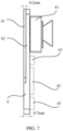
- FIG. 7 is a side view of the auxiliary circuit board and the TOF device shown in FIG. 5 ;
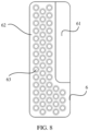
- FIG. 8 is a rear view of the auxiliary circuit board and the TOF device shown in FIG. 5 .
- the camera of the first camera module 1 is offset to the left side with respect to the first bracket 11
- the camera of the second camera module 2 is offset to the left side with respect to the second bracket 21, and therefore, to ensure that the TOF device 4 is in a middle position between the first camera module 1 and the second camera module 2, the auxiliary circuit board 6 is offset to the left side with respect to the spacing portion 5, and a right side of the auxiliary circuit board 6 is substantially aligned with a right side of the spacing portion 5, so as to avoid a structural conflict with the second bracket 21 of the second camera module 2. Therefore, the material removal portion 61 is formed only on the left side of the auxiliary circuit board 6 is formed.
- the material removal portion 61 when viewed from the rear view of the auxiliary circuit board 6 (namely, the view of FIG. 8 ), is substantially in a vertical rectangular shape, is located on a right side of the lower surface of the auxiliary circuit board 6, and is in an upper corner region.
- a length of the material removal portion 61 may be 1/2 to 4/5 of a length of the auxiliary circuit board 6, and a width of the material removal portion 61 may be 1/5 to 1/2 of the width of the auxiliary circuit board 6.
- the material removal portion of the auxiliary circuit board 6 is a non-wiring region, and a partially suspended portion (that is, a portion whose thickness becomes thinner) corresponding to the material removal portion 61 may be a wiring region.
- the lower surface of the auxiliary circuit board 6 are provided with solder joints 63 in a non-material removing portion 62, and is electrically connected to the mainboard 3 via the solder joints 63, and the solder joints 63 are densely distributed on the lower surface of the auxiliary circuit board 6 in a form of a dot matrix.
- a device on the upper surface and the solder joints 63 on the lower surface can be connected through an internal direction-changing circuit, that is, the whole upper surface of the auxiliary circuit board 6 can be provided with connecting points, and connecting points on the lower surface are concentrated on the non-material removing portion 62.
- the connecting points on the upper surface and the connecting points on the lower surface are conducted on the circuit through the direction-changing circuit inside the auxiliary circuit board 6.
- a depth of the material removal portion 61 can be controlled within 0.2-0.5 mm.
- a thickness of the auxiliary circuit board 6 is 0.7 mm
- the depth of the material removal portion 61 is 0.2 mm (see FIG. 7 ).
- the depth of the material removal portion 61 may be designed to be relatively large, for example, may be 0.3 mm, 0.4 mm, or another value, provided that structural strength of the partially suspended portion is not affected.
- a cross-sectional thickness of a portion thereof will be a sum of a thicknesses of the mainboard 3, the thicknesses of the auxiliary circuit board 6 and a thicknesses of the TOF device 4, and a sum of the thicknesses of the TOF device 4 and the thicknesses of the auxiliary circuit board 6 should be less than or equal to a height of the first camera module 1 and the second camera module 2 beyond the mainboard 3, so that the TOF device 4 does not exceed a height limit.
- the thickness of the auxiliary circuit board 6 is less than the thickness of the mainboard 3, so that a height of the TOF device 4 does not exceed the height of the first camera module 1 and the height of the second camera module 2.
- the TOF device 4 on the auxiliary circuit board 6 mainly includes a TOF lamp 41, a driver IC42, and peripheral capacitor and resistor 43.
- the TOF lamp 41 occupies 1/3 of the region of the auxiliary circuit board 6, the driver IC42 occupies a lower center region of the auxiliary circuit board 6, and a region between the TOF lamp 41 and the driver IC42 and a lower region of the driver IC42 are used to dispose the peripheral capacitor and resistor 43 (see FIG. 6 ).
- the auxiliary circuit board 6 may be centrally disposed with respect to the spacing portion 5, and the material removal portion 61 is formed on each of two sides of the auxiliary circuit board 6, and the material removal portion 61 on the left side corresponds to the first bracket 11, so that the structural conflict with the first bracket 11 can be avoided, and the material removal portion 61 on the right side corresponds to the second bracket 21, so that the structural conflict with the second bracket 21 can be avoided.
- each of the material removal portions 61 is substantially in a vertical rectangular shape, is located on the left side or the right side of the lower surface of the auxiliary circuit board 6, and is in the upper corner region.
- the non-material removing portion 62 on the lower surface of the auxiliary circuit board 6 is in a " ⁇ " shape.
- the widths of the left and right material removal portions 61 are relatively narrow, and a sum of the widths may be equal to the width of the material removal portion 61 in the foregoing first embodiment, and the other structures are substantially the same as those in the first embodiment. Please refer to the foregoing descriptions.
- This structure is suitable for a case in which cameras of two camera modules are not offset from the bracket; in other words, the cameras of the camera modules are located in a center of the bracket, and geometric centers thereof coincide with each other.
- the auxiliary circuit board 6 may be disposed and offset to the right side with respect to the spacing portion, and the material removal portion 61 is formed on the right side of the auxiliary circuit board 6, so that the structural conflict with the second bracket 21 can be avoided.
- the material removal portion 61 is substantially in a vertical rectangular shape, is located on the left side of the lower surface of the auxiliary circuit board 6, and is in the upper corner region.
- the rest of the structure is substantially the same as that in the first embodiment. Please refer to the foregoing descriptions. This structure is suitable for a case in which the cameras of the two camera modules are offset to the right side with respect to the bracket.
- an upper end and a lower end of the auxiliary circuit board 6 each may extend beyond the spacing portion 5 and then be connected to the mainboard 3.
- the material removal portion 61 on the left side and/or the material removal portion 61 on the right side of the auxiliary circuit board 6 mainly occupy/occupies a middle portion except the two ends of the auxiliary circuit board 6. When viewed from the rear view of the auxiliary circuit board 6.
- the auxiliary circuit board 6 has a larger overlapped area with the mainboard 3. On the one hand, connection strength between the two can be improved, and on the other hand, the auxiliary circuit board 6 of a larger size may adapt to various types of TOF devices 4, to facilitate circuit design, so as to better implement electrical connection.
- the material removal portion 61 on the auxiliary circuit board 6 may be processed and manufactured in various ways.
- the material removal portion 61 may be formed integrally with the auxiliary circuit board 6; or the auxiliary circuit board 6 may be formed first, and then, the material removal portion 61 may be processed and formed based on the auxiliary circuit board 6 through a subsequent process, for example, a partially material of the auxiliary circuit board 6 may be milled off via a cavity process, so as to form the required material removal portion 61.
- the auxiliary circuit board 6 may be formed by overlapping at least two layers of circuit boards.
- a structure of the auxiliary circuit board 6 may be a pressed two-layer, three-layer, or four-layer structure.
- a lower-layer circuit board is a rectangular circuit board with a notch corner
- an upper-layer circuit board is a complete rectangular circuit board.
- the notch corner of the lower-layer circuit board may form the material removal portion 61, and the TOF device 4 is disposed on the upper-layer circuit board, the upper-layer circuit board and the lower-layer circuit board are electrically connected, and the lower-layer circuit board and the mainboard 3 are further electrically connected, so that the TOF device 4 and the mainboard 3 are electrically connected.
- the solution may also be applicable to a mode of three lenses (an ultra wide angle lens, a zoom lens, and a main camera lens), a mode of four lenses (an ultra wide angle lens, a zoom lens, a main camera lens, and a depth of field auxiliary lens) or a mode of five lenses (an ultra wide angle lens, a zoom lens, a main camera lens, a depth of field auxiliary lens, and another lens), so that a third camera module, a fourth camera module, and a fifth camera module are further provided.
- the first camera module 1 and the second camera module 2 are disposed up and down, and in this case, the auxiliary circuit board 6 is also adjusted to be disposed laterally, and so on. Since there are many possible implementation manners, examples are not described herein again.
- the camera module structure provided in this application, by disposing hollowed-out mounting portions for the first camera module 1 and the second camera module 2, so that brackets of the two camera modules only extend beyond the mainboard 3 by a small distance after the two camera modules are mounted on the mainboard 3.
- the TOF device 4 is mounted by superimposing the auxiliary circuit board 6 on the spacing portion 5.
- the width of the auxiliary circuit board 6 is greater than the width of the spacing portion 5, there is sufficient space for mounting the TOF device 4, and the lower surface of the auxiliary circuit board 6 is provided with the material removal portion 61, and a portion in which the bracket of the first camera module 1 and/or the bracket of the bracket of the second camera module 2 are/is overlapped with the auxiliary circuit board 6 may be accommodated via the material removal portion 61, thereby avoiding a structural conflict with the bracket of the camera module beyond the mainboard 3.
- the width of the spacing portion 5 may be designed to be relatively small; to be specific, after the spacing between the two camera modules is further compressed, the TOF device 4 may still be normally mounted via the auxiliary circuit board 6 with the foregoing structure, thereby further narrowing the opening of the camera region. This is applicable to both the front-facing camera module and the rear-facing camera module.
- a lateral length that is of the front-facing camera module that is visible from the outside becomes smaller accordingly, to reduce an area that is of an upper left corner region of a screen and that is occupied by the entire front-facing camera module, and an area of a screen display region is further increased.
- This ensures a camera function and camera quality, increases a screen-to-body ratio, thereby improving use experience of a consumer.
- this reduces an area occupied by the TOF device 4 when the TOF device 4 is arranged on the mainboard 3, so that an internal structure is more compact and reasonable.
- this application further provides an electronic device.
- the electronic device may be specifically a mobile phone (see FIG. 1 ), a tablet computer, a wearable device, a vehicle-mounted device, an augmented reality (augmented reality, AR) /virtual reality (virtual reality, VR) device, a notebook computer, an ultra-mobile personal computer (ultra-mobile personal computer, UMPC), a netbook, a personal digital assistant (personal digital assistant, PDA), and the like.
- the electronic device includes a housing and a display screen, and the housing and/or the display screen are/is provided with a camera region.
- the camera module structure described above is provided in the camera region.
- the conventional technology Details are not described herein again.
Landscapes
- Engineering & Computer Science (AREA)
- Signal Processing (AREA)
- Multimedia (AREA)
- Computer Networks & Wireless Communication (AREA)
- Physics & Mathematics (AREA)
- General Physics & Mathematics (AREA)
- Radar, Positioning & Navigation (AREA)
- Remote Sensing (AREA)
- Human Computer Interaction (AREA)
- Camera Bodies And Camera Details Or Accessories (AREA)
- Studio Devices (AREA)
Abstract
Description
- This application claims priority to
Chinese Patent Application No. 202110924339.0, filed with the China National Intellectual Property Administration on August 12, 2021 - This application relates to the field of TOF technologies, and in particular, to a camera module structure. The present invention also relates to an electronic device provided with the camera module structure.
- In recent years, competition in the electronic device market has become more and more fierce, and consumers have higher and higher requirements for products. With continuous expansion of the application of the TOF (Time of flight) technology, a TOF image sensor has completed a technology evolution from CCD (Charge coupled device) to CMOS (Complementary Metal-Oxide-Semiconductor), and gradually becomes a standard configuration of many electronic products.
- A display screen of a product such as a mobile phone or a tablet computer is provided with a camera region. To avoid an excessive impact of the camera region on a screen-to-body ratio of the display screen, so as to ensure that a consumer can obtain better experience, an area that is of the display screen and that is occupied by the camera region should be as small as possible.
- Using a smartphone as an example, an edge portion of the display screen is generally provided with two or more front-facing camera modules, and these front-facing camera modules are mounted on a mainboard of the mobile phone. To narrow an opening of a camera region of a mobile phone screen, in addition to reducing sizes of the modules, another feasible design manner is to compress spacing between adjacent front-facing camera modules as much as possible.
- A front-facing TOF device on a smartphone is usually disposed between two adjacent front-facing camera modules. If the spacing between brackets of the adjacent front-facing camera module is too small, a width of the TOF device is relatively large, and the spacing between the brackets of the adjacent front-facing camera module brackets is relatively small, and consequently, the TOF device cannot be placed. Therefore, limited by a size of the TOF device, using this method to reduce the area of the imaging area has reached its limit.
- In view of the foregoing defect in a structure of the camera module, how to improve the structure of the camera module, to further reduce the area occupied by the camera region becomes a technical problem to be resolved by a person skilled in the art.
- An objective of this application is to provide a camera module structure. The camera module structure can further narrow an opening of a camera region, and reduce an area occupied by a TOF device when the TOF device is arranged on a mainboard.
- Another objective of this application is to provide an electronic device provided with the camera module structure.
- To achieve the foregoing objective, embodiments of this application provide a camera module structure. The camera module structure mainly includes a mainboard, a first camera module, a second camera module, and a TOF device, where the TOF device is located between the first camera module and the second camera module, the mainboard is provided with a first mounting portion and a second mounting portion that are hollowed-out, and the first camera module and the second camera module each are provided with a bracket and are respectively mounted to the first mounting portion and the second mounting portion via the brackets; and a spacing portion is formed between the first mounting portion and the second mounting portion, the TOF device is disposed on an auxiliary circuit board, a width of the auxiliary circuit board is greater than a width of the spacing portion, the auxiliary circuit board is located on an upper surface of the mainboard, and the auxiliary circuit board is connected to the mainboard and at least partially overlapped with the spacing portion.
- The mainboard is provided with a mounting portion for mounting the first camera module and the second camera module, and the auxiliary circuit board is superposed on the spacing portion of the mainboard, and the TOF device is mounted via the auxiliary circuit board. Because the width of the auxiliary circuit board is greater than the width of the spacing portion, there is sufficient space for mounting the TOF device, so that the width of the spacing portion can be designed to be relatively small. That is, after spacing between the two camera modules is further compressed, the TOF device may still be mounted normally via the auxiliary circuit board with an unique shape, to further narrow an opening of the camera region, increase a screen-to-body ratio, improve consumer experience, and reduce an area occupied when the TOF device is arranged on the mainboard, so that an internal structure is more compact and reasonable.
- Optionally, a region in which the auxiliary circuit board is overlapped with the bracket of the first camera module and/or a region in which the auxiliary circuit board is overlapped with the bracket of the second camera module are/is provided with a material removal portion whose depth is less than a thickness of the region on a lower surface, so that the auxiliary circuit board is partially suspended, and a portion in which the bracket of the first camera module and/or the bracket of the second camera module are/is overlapped with the auxiliary circuit board are/is accommodated via the material removal portion.
- By disposing the material removal portion on the lower surface of the auxiliary circuit board, a portion in which the bracket of the first camera module and/or a portion in which the bracket of the second camera module are/is overlapped with the auxiliary circuit board may be accommodated via the material removal portion, thereby avoiding a structural conflict with the bracket of the camera module beyond the mainboard; in other words, the auxiliary circuit board and the TOF device can be normally mounted even if the bracket of the camera module is relatively high.
- Optionally, the auxiliary circuit board is offset to the first camera module or the second camera module with respect to the spacing portion, and the material removal portion is located on one side of the auxiliary circuit board; or
the auxiliary circuit board is centrally disposed with respect to the spacing portion, and the material removal portion is formed on each of two sides of the auxiliary circuit board. - Optionally, the material removal portion is located in a corner region of a lower surface of the auxiliary circuit board, and a non-material removing portion of the lower surface of the auxiliary circuit board is in an "L" shape or a "⊥" shape.
- Optionally, a length of the material removal portion is 1/2 to 4/5 of a length of the auxiliary circuit board.
- Optionally, the material removal portion is 0.2-0.5 mm in depth.
- Optionally, a lower surface of the auxiliary circuit board is provided with solder joints on a non-material removing portion, and is electrically connected to the mainboard via the solder joints.
- Optionally, a material removal portion of the auxiliary circuit board is a non-wiring region, and a partially suspended portion of the auxiliary circuit board is a wiring region.
- Optionally, a sum of a thickness of the TOF device and a thickness of the auxiliary circuit board is less than or equal to a height of the first camera module and the second camera module beyond the mainboard.
- Optionally, the auxiliary circuit board is in a rectangular shape, an upper half portion of the auxiliary circuit board is partially overlapped with the spacing portion, and a lower half portion of the auxiliary circuit board extends beyond the spacing portion.
- Optionally, the auxiliary circuit board includes at least two layers of circuit boards which are overlapped, a lower-layer circuit board includes a notch corner, to form a material removal portion, and the TOF device is disposed on an upper-layer circuit board; and the upper-layer circuit board is electrically connected to the lower-layer circuit board, and the lower-layer circuit board is electrically connected to the mainboard.
- To achieve the another objective, this application provides an electronic device, including a housing and a display screen, where the housing and/or the display screen are/is provided with a camera region, the camera region is provided with a camera module, and the camera module has any one of the foregoing camera module structures.
- The electronic device provided in this application is provided with the camera module structure. Because the camera module structure has the foregoing technical effect, the electronic device with the camera module structure should also have the corresponding technical effect.
-
-
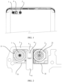
FIG. 1 is a schematic diagram of a portion of a smartphone provided with a camera module structure according to an embodiment of this application; -
FIG. 2 is a schematic a front view of a camera module structure disclosed in an embodiment of this application; -
FIG. 3 is an isometric view of the camera module structure shown inFIG. 2 ; -
FIG. 4 is a schematic diagram of a structure of a portion of a mainboard shown inFIG. 2 ; -
FIG. 5 is a schematic diagram of a position relationship between an auxiliary circuit board provided with a TOF device and each of a first camera module and a second camera module; -
FIG. 6 is a front view of the auxiliary circuit board and the TOF device shown inFIG. 5 ; -
FIG. 7 is a side view of the auxiliary circuit board and the TOF device shown inFIG. 5 ; and -
FIG. 8 is a rear view of the auxiliary circuit board and the TOF device shown inFIG. 5 . - 1.
First camera module 11.First bracket 2.Second camera module 21.Second bracket 3.Mainboard 31.First mounting portion 32. Second mounting portion 4.TOF device 41.TOF lamp 42. Driver IC 43. Peripheral capacitor andresistor 5.Spacing portion 6.Auxiliary circuit board 61.Material removal portion 62. Non-material removingportion 63. Solder joint - To enable a person skilled in the art to better understand solutions in this application, the following describes in detail this application with reference to accompanying drawings and specific implementations.
- Terms such as "upper", "lower", "inner", and "outer" are defined herein based on positional relationships shown in the accompanying drawings. Depending on different accompanying drawings, the corresponding positional relationships may also change, and therefore cannot be interpreted as an absolute limitation to the protection scope. Terms such as "first", and "second" are only used to distinguish one component from another with a same name, and does not necessarily require or suggest that there are any actual relationship or order between these components.
- As shown in
FIG. 1 , this embodiment provides a camera module structure applied to a smartphone. The smartphone is provided with a camera region at an upper edge position of a display screen of the smartphone, and the camera region is offset to a left side (certainly, the camera region may also be centered or offset to a right side). Because a dual-camera mode is enabled, afirst camera module 1 and asecond camera module 2 are provided inside the camera region. To enhance a camera function, aTOF device 4 is further provided. A TOF technology belongs to one of two-way ranging methods. A basic principle is that a time difference exists in this process in which a light pulse is continuously sent to a target, and then light returned from an object is received by a sensor, so that a distance between a transmitter and the measured object is calculated, and the TOF device is added, so that the camera module can fast and remotely obtain depth-of-field information with higher accuracy, thereby completing a wider range of 3D modeling. - Because the camera region occupies a normal display region of the display screen, generally, an area of the camera region should be as small as possible. Although an area occupied by two adjacent front-facing camera modules can be reduced by compressing lateral spacing between the two adjacent front-facing camera modules, if spacing between the
first camera module 1 and thesecond camera module 2 is too small, the TOF device cannot be normally mounted. - For this problem, a camera module structure is redesigned in this application, and in the camera module structure, a TOF device can still be mounted between two adjacent camera modules when spacing between the camera modules is relatively small, thereby further narrowing an opening of the camera region and increasing a screen-to-body ratio.
- As shown in
FIG. 2 andFIG. 3 , specifically, this camera module structure mainly includes amainboard 3 and afirst camera module 1, asecond camera module 2, aTOF device 4, and the like that are disposed on themainboard 3. - The
first camera module 1 and thesecond camera module 2 together form dual lenses, to implement a front-facing camera function. TheTOF device 4 is located between thefirst camera module 1 and thesecond camera module 2, and themainboard 3 is provided with a first mountingportion 31 and a second mountingportion 32 that are hollowed-out. Thefirst camera module 1 is provided with afirst bracket 11, thesecond camera module 2 is provided with asecond bracket 21, and thefirst camera module 1 and thesecond camera module 2 are respectively mounted on the first mountingportion 31 and the second mountingportion 32 via thefirst bracket 11 and thesecond bracket 21; projection shapes of the brackets of thefirst camera module 1 and thesecond camera module 2 are as shown inFIG. 2 ; and shapes of the first mountingportion 31 and the second mountingportion 32 that are hollowed-out are as shown inFIG. 3 , and are adapted to the brackets of thefirst camera module 1 and thesecond camera module 2, so that the first mountingportion 31 and the second mountingportion 32 can be placed in the brackets of thefirst camera module 1 and thesecond camera module 2. - By disposing the first mounting
portion 31 and the second mountingportion 32 that are hollowed-out on themainboard 3, the two camera modules can be located in themainboard 3 after mounting, and a height of the camera module is reduced as much as possible, so that the brackets of the two camera modules only extend beyond themainboard 3 by a relatively small distance, thereby creating an advantageous condition for mounting anauxiliary circuit board 6. Theauxiliary circuit board 6 is an added circuit board with a relatively small volume, and is connected to themainboard 3 and located between thefirst camera module 1 and thesecond camera module 2. Via theauxiliary circuit board 6, theTOF device 4 can still be mounted when spacing between thefirst camera module 1 and thesecond camera module 2 is relatively small, thereby reducing an area occupied by the entire camera module structure. - The first mounting
portion 31 on themainboard 3 is in a circumferential closed shape, and the second mountingportion 32 adjacent to the first mountingportion 31 is in an upper open shape (seeFIG. 4 ). The first mountingportion 31 and the second mountingportion 32 are spaced from each other via avertical spacing portion 5. Theauxiliary circuit board 6 is substantially in a rectangular shape and has a width greater than a width of thespacing portion 5. Theauxiliary circuit board 6 is located on an upper surface of themainboard 3. An upper half portion of theauxiliary circuit board 6 and thespacing portion 5 are partially overlapped. A lower half portion of theauxiliary circuit board 6 extends beyond the spacingportion 5 and is overlapped with a part of the mainboard that is outside thespacing portion 5. TheTOF device 4 is mounted on an upper surface of theauxiliary circuit board 6. During assembly, theTOF device 4 is mounted on themainboard 3 via theauxiliary circuit board 6 and is electrically connected to themainboard 3 via the auxiliary circuit board 6 (seeFIG. 5 ). - Still referring to
FIG. 5 , cameras and the brackets of thefirst camera module 1 and thesecond camera module 2 are generally an integral structure. During assembly, thefirst camera module 1 and thesecond camera module 2 each are first placed in the first mountingportion 31 and the second mountingportion 32, and then theauxiliary circuit board 6 is mounted. A left side of theauxiliary circuit board 6 is partially overlapped with thefirst bracket 11 of thefirst camera module 1, a region in which theauxiliary circuit board 6 is overlapped with thefirst bracket 11 is provided with anmaterial removal portion 61 whose depth is less than a thickness of the region on a lower surface, and theauxiliary circuit board 6 can be partially suspended by thematerial removal portion 61, so that a portion in which thefirst bracket 11 is overlapped with theauxiliary circuit board 6 is accommodated by thematerial removal portion 61, to avoid a structural conflict between theauxiliary circuit board 6 and thefirst bracket 11. - It is not difficult to understand that the mainboard of the smartphone also includes another part. Because improvement of this application is mainly concentrated in the camera region, only a structure of a portion of the mainboard corresponding to the camera region is shown in the accompanying drawings, and the another part of the mainboard is omitted.
- Refer to
FIG. 6 to FIG. 8 .FIG. 6 is a front view of the auxiliary circuit board and the TOF device shown inFIG. 5 ;FIG. 7 is a side view of the auxiliary circuit board and the TOF device shown inFIG. 5 ; andFIG. 8 is a rear view of the auxiliary circuit board and the TOF device shown inFIG. 5 . - In this embodiment, the camera of the
first camera module 1 is offset to the left side with respect to thefirst bracket 11, and the camera of thesecond camera module 2 is offset to the left side with respect to thesecond bracket 21, and therefore, to ensure that theTOF device 4 is in a middle position between thefirst camera module 1 and thesecond camera module 2, theauxiliary circuit board 6 is offset to the left side with respect to thespacing portion 5, and a right side of theauxiliary circuit board 6 is substantially aligned with a right side of thespacing portion 5, so as to avoid a structural conflict with thesecond bracket 21 of thesecond camera module 2. Therefore, thematerial removal portion 61 is formed only on the left side of theauxiliary circuit board 6 is formed. - Specifically, when viewed from the rear view of the auxiliary circuit board 6 (namely, the view of
FIG. 8 ), thematerial removal portion 61 is substantially in a vertical rectangular shape, is located on a right side of the lower surface of theauxiliary circuit board 6, and is in an upper corner region. - For different products, areas of the
auxiliary circuit board 6 overlapped with thefirst bracket 11 are different. Therefore, the area of thematerial removal portion 61 also changes. For example, a length of thematerial removal portion 61 may be 1/2 to 4/5 of a length of theauxiliary circuit board 6, and a width of thematerial removal portion 61 may be 1/5 to 1/2 of the width of theauxiliary circuit board 6. - The material removal portion of the
auxiliary circuit board 6 is a non-wiring region, and a partially suspended portion (that is, a portion whose thickness becomes thinner) corresponding to thematerial removal portion 61 may be a wiring region. The lower surface of theauxiliary circuit board 6 are provided withsolder joints 63 in a non-material removingportion 62, and is electrically connected to themainboard 3 via the solder joints 63, and the solder joints 63 are densely distributed on the lower surface of theauxiliary circuit board 6 in a form of a dot matrix. - If the partially suspended portion of the
auxiliary circuit board 6 needs to be wired, a device on the upper surface and the solder joints 63 on the lower surface can be connected through an internal direction-changing circuit, that is, the whole upper surface of theauxiliary circuit board 6 can be provided with connecting points, and connecting points on the lower surface are concentrated on the non-material removingportion 62. The connecting points on the upper surface and the connecting points on the lower surface are conducted on the circuit through the direction-changing circuit inside theauxiliary circuit board 6. To avoid that an excessive depth of thematerial removal portion 61 affects an internal wiring of the partially suspended portion, a depth of thematerial removal portion 61 can be controlled within 0.2-0.5 mm. In this embodiment, a thickness of theauxiliary circuit board 6 is 0.7 mm, and the depth of thematerial removal portion 61 is 0.2 mm (seeFIG. 7 ). - If the partially suspended portion of the
auxiliary circuit board 6 is a non-wiring region, is mainly configured to support theTOF device 4, and serves as a mounting foundation for theTOF device 4, the depth of thematerial removal portion 61 may be designed to be relatively large, for example, may be 0.3 mm, 0.4 mm, or another value, provided that structural strength of the partially suspended portion is not affected. - After the
auxiliary circuit board 6 is added onto thespacing portion 5 of themainboard 3, a cross-sectional thickness of a portion thereof will be a sum of a thicknesses of themainboard 3, the thicknesses of theauxiliary circuit board 6 and a thicknesses of theTOF device 4, and a sum of the thicknesses of theTOF device 4 and the thicknesses of theauxiliary circuit board 6 should be less than or equal to a height of thefirst camera module 1 and thesecond camera module 2 beyond themainboard 3, so that theTOF device 4 does not exceed a height limit. In this embodiment, the thickness of theauxiliary circuit board 6 is less than the thickness of themainboard 3, so that a height of theTOF device 4 does not exceed the height of thefirst camera module 1 and the height of thesecond camera module 2. - The
TOF device 4 on theauxiliary circuit board 6 mainly includes aTOF lamp 41, a driver IC42, and peripheral capacitor andresistor 43. TheTOF lamp 41 occupies 1/3 of the region of theauxiliary circuit board 6, the driver IC42 occupies a lower center region of theauxiliary circuit board 6, and a region between theTOF lamp 41 and the driver IC42 and a lower region of the driver IC42 are used to dispose the peripheral capacitor and resistor 43 (seeFIG. 6 ). - In another embodiment, the
auxiliary circuit board 6 may be centrally disposed with respect to thespacing portion 5, and thematerial removal portion 61 is formed on each of two sides of theauxiliary circuit board 6, and thematerial removal portion 61 on the left side corresponds to thefirst bracket 11, so that the structural conflict with thefirst bracket 11 can be avoided, and thematerial removal portion 61 on the right side corresponds to thesecond bracket 21, so that the structural conflict with thesecond bracket 21 can be avoided. When viewed from the rear view of theauxiliary circuit board 6, each of thematerial removal portions 61 is substantially in a vertical rectangular shape, is located on the left side or the right side of the lower surface of theauxiliary circuit board 6, and is in the upper corner region. Because twomaterial removal portions 61 are disposed on the left side and the right side, the non-material removingportion 62 on the lower surface of theauxiliary circuit board 6 is in a "⊥" shape. The widths of the left and rightmaterial removal portions 61 are relatively narrow, and a sum of the widths may be equal to the width of thematerial removal portion 61 in the foregoing first embodiment, and the other structures are substantially the same as those in the first embodiment. Please refer to the foregoing descriptions. This structure is suitable for a case in which cameras of two camera modules are not offset from the bracket; in other words, the cameras of the camera modules are located in a center of the bracket, and geometric centers thereof coincide with each other. - In still another embodiment, the
auxiliary circuit board 6 may be disposed and offset to the right side with respect to the spacing portion, and thematerial removal portion 61 is formed on the right side of theauxiliary circuit board 6, so that the structural conflict with thesecond bracket 21 can be avoided. When viewed from the rear view of theauxiliary circuit board 6, thematerial removal portion 61 is substantially in a vertical rectangular shape, is located on the left side of the lower surface of theauxiliary circuit board 6, and is in the upper corner region. The rest of the structure is substantially the same as that in the first embodiment. Please refer to the foregoing descriptions. This structure is suitable for a case in which the cameras of the two camera modules are offset to the right side with respect to the bracket. - In another embodiment, an upper end and a lower end of the
auxiliary circuit board 6 each may extend beyond the spacingportion 5 and then be connected to themainboard 3. In this structure, thematerial removal portion 61 on the left side and/or thematerial removal portion 61 on the right side of theauxiliary circuit board 6 mainly occupy/occupies a middle portion except the two ends of theauxiliary circuit board 6. When viewed from the rear view of theauxiliary circuit board 6. If thematerial removal portion 61 is located on the left side of theauxiliary circuit board 6, the non-material removingportion 62 on theauxiliary circuit board 6 is in a "]" shape; or if thematerial removal portion 61 is located on the right side of theauxiliary circuit board 6, the non-material removingportion 62 on theauxiliary circuit board 6 is in a "[" shape; or ifmaterial removal portions 61 are located on the left side and the right side of theauxiliary circuit board 6, the non-material removingportion 62 on theauxiliary circuit board 6 is in an "I" shape. In this structure, theauxiliary circuit board 6 has a larger overlapped area with themainboard 3. On the one hand, connection strength between the two can be improved, and on the other hand, theauxiliary circuit board 6 of a larger size may adapt to various types ofTOF devices 4, to facilitate circuit design, so as to better implement electrical connection. - The
material removal portion 61 on theauxiliary circuit board 6 may be processed and manufactured in various ways. Thematerial removal portion 61 may be formed integrally with theauxiliary circuit board 6; or theauxiliary circuit board 6 may be formed first, and then, thematerial removal portion 61 may be processed and formed based on theauxiliary circuit board 6 through a subsequent process, for example, a partially material of theauxiliary circuit board 6 may be milled off via a cavity process, so as to form the requiredmaterial removal portion 61. - In addition, the
auxiliary circuit board 6 may be formed by overlapping at least two layers of circuit boards. Specifically, a structure of theauxiliary circuit board 6 may be a pressed two-layer, three-layer, or four-layer structure. For example, in a two-layer overlapped circuit board, a lower-layer circuit board is a rectangular circuit board with a notch corner, and an upper-layer circuit board is a complete rectangular circuit board. In this way, after two layers of circuit boards are overlapped, the notch corner of the lower-layer circuit board may form thematerial removal portion 61, and theTOF device 4 is disposed on the upper-layer circuit board, the upper-layer circuit board and the lower-layer circuit board are electrically connected, and the lower-layer circuit board and themainboard 3 are further electrically connected, so that theTOF device 4 and themainboard 3 are electrically connected. - The forgoing embodiment is merely a preferred solution of this application, and is not specifically limited thereto. Based on this solution, a targeted adjustment may be made based on an actual requirement, to obtain different implementations. For example, in addition to a mode of front-facing dual lenses, the solution may also be applicable to a mode of three lenses (an ultra wide angle lens, a zoom lens, and a main camera lens), a mode of four lenses (an ultra wide angle lens, a zoom lens, a main camera lens, and a depth of field auxiliary lens) or a mode of five lenses (an ultra wide angle lens, a zoom lens, a main camera lens, a depth of field auxiliary lens, and another lens), so that a third camera module, a fourth camera module, and a fifth camera module are further provided. Alternatively, the
first camera module 1 and thesecond camera module 2 are disposed up and down, and in this case, theauxiliary circuit board 6 is also adjusted to be disposed laterally, and so on. Since there are many possible implementation manners, examples are not described herein again. - As shown in
FIG. 3 andFIG. 5 , in the camera module structure provided in this application, by disposing hollowed-out mounting portions for thefirst camera module 1 and thesecond camera module 2, so that brackets of the two camera modules only extend beyond themainboard 3 by a small distance after the two camera modules are mounted on themainboard 3. TheTOF device 4 is mounted by superimposing theauxiliary circuit board 6 on thespacing portion 5. Because the width of theauxiliary circuit board 6 is greater than the width of thespacing portion 5, there is sufficient space for mounting theTOF device 4, and the lower surface of theauxiliary circuit board 6 is provided with thematerial removal portion 61, and a portion in which the bracket of thefirst camera module 1 and/or the bracket of the bracket of thesecond camera module 2 are/is overlapped with theauxiliary circuit board 6 may be accommodated via thematerial removal portion 61, thereby avoiding a structural conflict with the bracket of the camera module beyond themainboard 3. In this way, the width of thespacing portion 5 may be designed to be relatively small; to be specific, after the spacing between the two camera modules is further compressed, theTOF device 4 may still be normally mounted via theauxiliary circuit board 6 with the foregoing structure, thereby further narrowing the opening of the camera region. This is applicable to both the front-facing camera module and the rear-facing camera module. - As shown in
FIG. 1 , when the camera module structure is applied to the front-facing camera module of the smartphone, because the spacing between thefirst camera module 1 and thesecond camera module 2 is further reduced, a lateral length that is of the front-facing camera module that is visible from the outside becomes smaller accordingly, to reduce an area that is of an upper left corner region of a screen and that is occupied by the entire front-facing camera module, and an area of a screen display region is further increased. This ensures a camera function and camera quality, increases a screen-to-body ratio, thereby improving use experience of a consumer. In addition, this reduces an area occupied by theTOF device 4 when theTOF device 4 is arranged on themainboard 3, so that an internal structure is more compact and reasonable. - In addition to the camera module structure, this application further provides an electronic device. The electronic device may be specifically a mobile phone (see
FIG. 1 ), a tablet computer, a wearable device, a vehicle-mounted device, an augmented reality (augmented reality, AR) /virtual reality (virtual reality, VR) device, a notebook computer, an ultra-mobile personal computer (ultra-mobile personal computer, UMPC), a netbook, a personal digital assistant (personal digital assistant, PDA), and the like. The electronic device includes a housing and a display screen, and the housing and/or the display screen are/is provided with a camera region. The camera module structure described above is provided in the camera region. For another structure of the electronic device, refer to the conventional technology. Details are not described herein again. - The foregoing describes the camera module structure and the electronic device provided in this application in detail. A principle and an implementation of this application are described herein based on specific examples. The descriptions about the embodiments are merely provided to help understand a core idea of this application. It should be noted that a person of ordinary skill in the art may make several improvements or modifications without departing from the principle of this application, and the improvements or modifications shall fall within the protection scope of this application.
Claims (21)
- A camera module structure, comprising a mainboard, a first camera module, a second camera module, and a time of flight TOF device, wherein the TOF device is located between the first camera module and the second camera module, the mainboard is provided with a first mounting portion and a second mounting portion that are hollowed-out, and the first camera module and the second camera module each are provided with a bracket and are respectively mounted to the first mounting portion and the second mounting portion via the brackets; and the mainboard comprises a spacing portion for separation between the first mounting portion and the second mounting portion, the TOF device is disposed on an upper surface of an auxiliary circuit board, a width of the auxiliary circuit board is greater than a width of the spacing portion, the auxiliary circuit board is located on an upper surface of the mainboard, and the auxiliary circuit board is connected to the mainboard and at least partially overlapped with the spacing portion.
- The camera module structure according to claim 1, wherein a region in which the auxiliary circuit board is overlapped with the bracket of the first camera module and/or a region in which the auxiliary circuit board is overlapped with the bracket of the second camera module are/is provided with a material removal portion whose depth is less than a thickness of the region on a lower surface, so that the auxiliary circuit board is partially suspended, and a portion in which the bracket of the first camera module and/or a portion in which the bracket of the second camera module are/is overlapped with the auxiliary circuit board are/is accommodated via the material removal portion.
- The camera module structure according to claim 1, wherein the auxiliary circuit board is offset to the first camera module or the second camera module with respect to the spacing portion, and the material removal portion is located on one side of the auxiliary circuit board; or
the auxiliary circuit board is centrally disposed with respect to the spacing portion, and the material removal portion is formed on each of two sides of the auxiliary circuit board. - The camera module structure according to claim 3, wherein the material removal portion is located in a corner region of a lower surface of the auxiliary circuit board, and a non-material removing portion of the lower surface of the auxiliary circuit board is in an "L" shape or a "1" shape.
- The camera module structure according to claim 4, wherein a length of the material removal portion is 1/2 to 4/5 of a length of the auxiliary circuit board; and/or the material removal portion is 0.2-0.5 mm in depth.
- The camera module structure according to claim 1, wherein a lower surface of the auxiliary circuit board is provided with solder joints on a non-material removing portion, and is electrically connected to the mainboard via the solder joints.
- The camera module structure according to claim 6, wherein a material removal portion of the auxiliary circuit board is a non-wiring region, and a partially suspended portion of the auxiliary circuit board is a wiring region.
- The camera module structure according to claim 1, wherein a sum of a thickness of the TOF device and a thickness of the auxiliary circuit board is less than or equal to a height of the first camera module and the second camera module beyond the mainboard.
- The camera module structure according to claim 1, wherein the auxiliary circuit board is in a rectangular shape, an upper half portion of the auxiliary circuit board is partially overlapped with the spacing portion, and a lower half portion of the auxiliary circuit board extends beyond the spacing portion.
- The camera module structure according to claim 1, wherein the auxiliary circuit board comprises at least two layers of circuit boards which are overlapped, a lower-layer circuit board comprises a notch corner, to form a material removal portion, and the TOF device is disposed on an upper-layer circuit board; and the upper-layer circuit board is electrically connected to the lower-layer circuit board, and the lower-layer circuit board is electrically connected to the mainboard.
- An electronic device, comprising a housing and/or a display screen, wherein the housing and/or the display screen are/is provided with a camera region, the camera region is provided with a camera module, and the camera module has the camera module structure according to any one of claims 1 to 10.
- A camera module structure, comprising a mainboard, a first camera module, a second camera module, and a time of flight TOF device, wherein the TOF device is located between the first camera module and the second camera module, the mainboard is provided with a first mounting portion and a second mounting portion that are hollowed-out, and the first camera module and the second camera module each are provided with a bracket and are respectively mounted to the first mounting portion and the second mounting portion via the brackets; the mainboard comprises a spacing portion for separation between the first mounting portion and the second mounting portion, the TOF device is disposed on an upper surface of an auxiliary circuit board, a width of the auxiliary circuit board is greater than a width of the spacing portion, the auxiliary circuit board is located on an upper surface of the mainboard, and the auxiliary circuit board is connected to the mainboard and at least partially overlapped with the spacing portion; a region in which the auxiliary circuit board is overlapped with the bracket of the first camera module and/or a region in which the auxiliary circuit board is overlapped with the bracket of the second camera module are/is provided with a material removal portion whose depth is less than a thickness of the region on a lower surface, so that the auxiliary circuit board is partially suspended, and a portion in which the bracket of the first camera module and/or a portion in which the bracket of the second camera module are/is overlapped with the auxiliary circuit board are/is accommodated via the material removal portion.
- The camera module structure according to claim 12, wherein the auxiliary circuit board is offset to the first camera module or the second camera module with respect to the spacing portion, and the material removal portion is located on one side of the auxiliary circuit board; or
the auxiliary circuit board is centrally disposed with respect to the spacing portion, and the material removal portion is formed on each of two sides of the auxiliary circuit board. - The camera module structure according to claim 13, wherein the material removal portion is located in a corner region of a lower surface of the auxiliary circuit board, and a non-material removing portion of the lower surface of the auxiliary circuit board is in an "L" shape or a "1" shape.
- The camera module structure according to claim 14, wherein a length of the material removal portion is f1/2 to 4/5 of a length of the auxiliary circuit board; and/orthe material removal portion is 0.2-0.5 mm in depth.
- The camera module structure according to claim 12, wherein a lower surface of the auxiliary circuit board is provided with solder joints on a non-material removing portion, and is electrically connected to the mainboard via the solder joints.
- The camera module structure according to claim 12, wherein the material removal portion of the auxiliary circuit board is a non-wiring region, and a partially suspended portion of the auxiliary circuit board is a wiring region.
- The camera module structure according to claim 12, wherein a sum of a thickness of the TOF device and a thickness of the auxiliary circuit board is less than or equal to a height of the first camera module and the second camera module beyond the mainboard.
- The camera module structure according to claim 12, wherein the auxiliary circuit board is in a rectangular shape, an upper half portion of the auxiliary circuit board is partially overlapped with the spacing portion, and a lower half portion of the auxiliary circuit board extends beyond the spacing portion.
- The camera module structure according to claim 12, wherein the auxiliary circuit board comprises at least two layers of circuit boards which are overlapped, a lower-layer circuit board comprises a notch corner, to form the material removal portion, and the TOF device is disposed on an upper-layer circuit board; and the upper-layer circuit board is electrically connected to the lower-layer circuit board, and the lower-layer circuit board is electrically connected to the mainboard.
- An electronic device, comprising a housing and/or a display screen, wherein the housing and/or the display screen are/is provided with a camera region, the camera region is provided with a camera module, and the camera module has the camera module structure according to any one of claims 12 to 20.
Applications Claiming Priority (2)
| Application Number | Priority Date | Filing Date | Title |
|---|---|---|---|
| CN202110924339.0A CN113726995B (en) | 2021-08-12 | 2021-08-12 | Camera module structure and electronic equipment |
| PCT/CN2022/092927 WO2023016013A1 (en) | 2021-08-12 | 2022-05-16 | Camera module structure and electronic device |
Publications (3)
| Publication Number | Publication Date |
|---|---|
| EP4156670A1 true EP4156670A1 (en) | 2023-03-29 |
| EP4156670A4 EP4156670A4 (en) | 2023-12-06 |
| EP4156670B1 EP4156670B1 (en) | 2024-09-04 |
Family
ID=78675682
Family Applications (1)
| Application Number | Title | Priority Date | Filing Date |
|---|---|---|---|
| EP22799829.1A Active EP4156670B1 (en) | 2021-08-12 | 2022-05-16 | Camera module structure and electronic device |
Country Status (4)
| Country | Link |
|---|---|
| US (1) | US12081859B2 (en) |
| EP (1) | EP4156670B1 (en) |
| CN (1) | CN113726995B (en) |
| WO (1) | WO2023016013A1 (en) |
Families Citing this family (2)
| Publication number | Priority date | Publication date | Assignee | Title |
|---|---|---|---|---|
| CN113726995B (en) * | 2021-08-12 | 2022-06-10 | 荣耀终端有限公司 | Camera module structure and electronic equipment |
| CN115542506B (en) * | 2022-03-01 | 2023-08-08 | 荣耀终端有限公司 | Optical adjustment structure and camera equipment |
Family Cites Families (18)
| Publication number | Priority date | Publication date | Assignee | Title |
|---|---|---|---|---|
| KR101070591B1 (en) * | 2009-06-25 | 2011-10-06 | (주)실리콘화일 | distance measuring apparatus having dual stereo camera |
| KR101848871B1 (en) * | 2011-08-03 | 2018-04-13 | 엘지전자 주식회사 | Mobile terminal |
| CN105225628B (en) * | 2014-06-19 | 2017-10-24 | 元太科技工业股份有限公司 | Display device, display module and pixel structure thereof |
| US10477157B1 (en) * | 2016-03-02 | 2019-11-12 | Meta View, Inc. | Apparatuses, methods and systems for a sensor array adapted for vision computing |
| KR102867955B1 (en) * | 2017-02-15 | 2025-10-10 | 삼성전자주식회사 | Camera module having lens barrells |
| KR102204596B1 (en) * | 2017-06-02 | 2021-01-19 | 삼성전자주식회사 | Processor, image processing device comprising the same, and method for image processing |
| CN109688298B (en) * | 2017-10-18 | 2024-03-22 | 宁波舜宇光电信息有限公司 | Camera module array and corresponding integrated substrate |
| CN108418915A (en) * | 2018-02-28 | 2018-08-17 | 广东欧珀移动通信有限公司 | Electronic components and electronic equipment |
| CN110233951B (en) * | 2018-03-06 | 2021-02-19 | Oppo广东移动通信有限公司 | Camera module, camera assembly and electronic device |
| CN208572292U (en) * | 2018-03-18 | 2019-03-01 | 宁波舜宇光电信息有限公司 | Depth information camera module and its base assembly and electronic equipment |
| CN111567021B (en) * | 2018-03-20 | 2021-06-01 | 华为技术有限公司 | Terminal |
| CN111416973A (en) * | 2019-01-08 | 2020-07-14 | 三赢科技(深圳)有限公司 | Three-dimensional sensing device |
| US10585194B1 (en) * | 2019-01-15 | 2020-03-10 | Shenzhen Guangjian Technology Co., Ltd. | Switchable diffuser projection systems and methods |
| CN109714516A (en) * | 2019-02-19 | 2019-05-03 | 昆山丘钛微电子科技有限公司 | TOF camera module and electronic product |
| CN110798550A (en) * | 2019-06-28 | 2020-02-14 | RealMe重庆移动通信有限公司 | Electronic device |
| CN110297378B (en) * | 2019-06-30 | 2021-08-17 | Oppo广东移动通信有限公司 | Photographing device, electronic device, and control method of electronic device |
| CN213661669U (en) * | 2020-08-17 | 2021-07-09 | 华为技术有限公司 | Electronic device |
| CN113726995B (en) * | 2021-08-12 | 2022-06-10 | 荣耀终端有限公司 | Camera module structure and electronic equipment |
-
2021
- 2021-08-12 CN CN202110924339.0A patent/CN113726995B/en active Active
-
2022
- 2022-05-16 WO PCT/CN2022/092927 patent/WO2023016013A1/en not_active Ceased
- 2022-05-16 EP EP22799829.1A patent/EP4156670B1/en active Active
- 2022-05-16 US US17/926,946 patent/US12081859B2/en active Active
Also Published As
| Publication number | Publication date |
|---|---|
| US12081859B2 (en) | 2024-09-03 |
| EP4156670B1 (en) | 2024-09-04 |
| EP4156670A4 (en) | 2023-12-06 |
| WO2023016013A1 (en) | 2023-02-16 |
| US20240187721A1 (en) | 2024-06-06 |
| CN113726995A (en) | 2021-11-30 |
| CN113726995B (en) | 2022-06-10 |
Similar Documents
| Publication | Publication Date | Title |
|---|---|---|
| US12081859B2 (en) | Camera module structure and electronic device | |
| US10270952B2 (en) | Imaging module with two cameras and electronic device | |
| US11245207B2 (en) | Stack structure of printed circuit boards using interposer and electronic device including the same | |
| US20220283409A1 (en) | Camera Lens, Camera Module, and Electronic Device | |
| KR20250093280A (en) | Camera module and optical instrument including the same | |
| EP3993369B1 (en) | Camera module and terminal device | |
| EP4266663B1 (en) | Camera assembly and electronic device | |
| US10425562B2 (en) | Three-dimensional image sensing module with a low z-height | |
| TW201917480A (en) | Lens driving apparatus, photographing module and electronic device | |
| EP3825990A1 (en) | Flexible screen module, terminal device and photographing method | |
| CN106161897B (en) | A camera and mobile terminal | |
| CN107454297A (en) | A kind of infrared photography module and camera device | |
| US20240244891A1 (en) | Light emitting display device | |
| CN203289497U (en) | Portable electronic device | |
| US11750903B2 (en) | Electronic device | |
| US20190126575A1 (en) | Imaging lens element, camera module, and electronic device | |
| CN220671792U (en) | Light path turning element, camera module and electronic device | |
| CN107948368A (en) | A chip, module and electronic device | |
| US12455435B2 (en) | Lens element, imaging lens assembly, camera module and electronic device | |
| US20230246395A1 (en) | Electronic device including shielding connector structure | |
| US11711891B2 (en) | Lens module mounting on rigid-flex printed circuit board | |
| US20250120011A1 (en) | Electronic element assembly, image sensor module, camera module and electronic device | |
| TWI423746B (en) | Circuit layout of image capturing device | |
| CN224247971U (en) | Optical lens element, imaging lens and electronic device | |
| JP3209652U (en) | Shooting module |
Legal Events
| Date | Code | Title | Description |
|---|---|---|---|
| STAA | Information on the status of an ep patent application or granted ep patent |
Free format text: STATUS: UNKNOWN |
|
| STAA | Information on the status of an ep patent application or granted ep patent |
Free format text: STATUS: THE INTERNATIONAL PUBLICATION HAS BEEN MADE |
|
| PUAI | Public reference made under article 153(3) epc to a published international application that has entered the european phase |
Free format text: ORIGINAL CODE: 0009012 |
|
| STAA | Information on the status of an ep patent application or granted ep patent |
Free format text: STATUS: REQUEST FOR EXAMINATION WAS MADE |
|
| 17P | Request for examination filed |
Effective date: 20221114 |
|
| AK | Designated contracting states |
Kind code of ref document: A1 Designated state(s): AL AT BE BG CH CY CZ DE DK EE ES FI FR GB GR HR HU IE IS IT LI LT LU LV MC MK MT NL NO PL PT RO RS SE SI SK SM TR |
|
| REG | Reference to a national code |
Ref legal event code: R079 Free format text: PREVIOUS MAIN CLASS: H04N0005225000 Ref country code: DE Ref legal event code: R079 Ref document number: 602022005922 Country of ref document: DE Free format text: PREVIOUS MAIN CLASS: H04N0005225000 Ipc: H04N0023450000 |
|
| A4 | Supplementary search report drawn up and despatched |
Effective date: 20231107 |
|
| RIC1 | Information provided on ipc code assigned before grant |
Ipc: H04N 23/50 20230101ALI20231031BHEP Ipc: H04M 1/02 20060101ALI20231031BHEP Ipc: H04N 23/57 20230101ALI20231031BHEP Ipc: H04N 23/45 20230101AFI20231031BHEP |
|
| GRAP | Despatch of communication of intention to grant a patent |
Free format text: ORIGINAL CODE: EPIDOSNIGR1 |
|
| STAA | Information on the status of an ep patent application or granted ep patent |
Free format text: STATUS: GRANT OF PATENT IS INTENDED |
|
| RIC1 | Information provided on ipc code assigned before grant |
Ipc: G01S 7/481 20060101ALI20240312BHEP Ipc: H04N 23/50 20230101ALI20240312BHEP Ipc: H04M 1/02 20060101ALI20240312BHEP Ipc: H04N 23/57 20230101ALI20240312BHEP Ipc: H04N 23/45 20230101AFI20240312BHEP |
|
| DAV | Request for validation of the european patent (deleted) | ||
| DAX | Request for extension of the european patent (deleted) | ||
| INTG | Intention to grant announced |
Effective date: 20240402 |
|
| GRAS | Grant fee paid |
Free format text: ORIGINAL CODE: EPIDOSNIGR3 |
|
| GRAA | (expected) grant |
Free format text: ORIGINAL CODE: 0009210 |
|
| STAA | Information on the status of an ep patent application or granted ep patent |
Free format text: STATUS: THE PATENT HAS BEEN GRANTED |
|
| AK | Designated contracting states |
Kind code of ref document: B1 Designated state(s): AL AT BE BG CH CY CZ DE DK EE ES FI FR GB GR HR HU IE IS IT LI LT LU LV MC MK MT NL NO PL PT RO RS SE SI SK SM TR |
|
| REG | Reference to a national code |
Ref country code: GB Ref legal event code: FG4D |
|
| REG | Reference to a national code |
Ref country code: CH Ref legal event code: EP |
|
| REG | Reference to a national code |
Ref country code: IE Ref legal event code: FG4D |
|
| REG | Reference to a national code |
Ref country code: DE Ref legal event code: R096 Ref document number: 602022005922 Country of ref document: DE |
|
| REG | Reference to a national code |
Ref country code: NL Ref legal event code: FP |
|
| REG | Reference to a national code |
Ref country code: LT Ref legal event code: MG9D |
|
| PG25 | Lapsed in a contracting state [announced via postgrant information from national office to epo] |
Ref country code: NO Free format text: LAPSE BECAUSE OF FAILURE TO SUBMIT A TRANSLATION OF THE DESCRIPTION OR TO PAY THE FEE WITHIN THE PRESCRIBED TIME-LIMIT Effective date: 20241204 |
|
| PG25 | Lapsed in a contracting state [announced via postgrant information from national office to epo] |
Ref country code: GR Free format text: LAPSE BECAUSE OF FAILURE TO SUBMIT A TRANSLATION OF THE DESCRIPTION OR TO PAY THE FEE WITHIN THE PRESCRIBED TIME-LIMIT Effective date: 20241205 Ref country code: FI Free format text: LAPSE BECAUSE OF FAILURE TO SUBMIT A TRANSLATION OF THE DESCRIPTION OR TO PAY THE FEE WITHIN THE PRESCRIBED TIME-LIMIT Effective date: 20240904 |
|
| PG25 | Lapsed in a contracting state [announced via postgrant information from national office to epo] |
Ref country code: BG Free format text: LAPSE BECAUSE OF FAILURE TO SUBMIT A TRANSLATION OF THE DESCRIPTION OR TO PAY THE FEE WITHIN THE PRESCRIBED TIME-LIMIT Effective date: 20240904 |
|
| PG25 | Lapsed in a contracting state [announced via postgrant information from national office to epo] |
Ref country code: LV Free format text: LAPSE BECAUSE OF FAILURE TO SUBMIT A TRANSLATION OF THE DESCRIPTION OR TO PAY THE FEE WITHIN THE PRESCRIBED TIME-LIMIT Effective date: 20240904 |
|
| PG25 | Lapsed in a contracting state [announced via postgrant information from national office to epo] |
Ref country code: HR Free format text: LAPSE BECAUSE OF FAILURE TO SUBMIT A TRANSLATION OF THE DESCRIPTION OR TO PAY THE FEE WITHIN THE PRESCRIBED TIME-LIMIT Effective date: 20240904 |
|
| PG25 | Lapsed in a contracting state [announced via postgrant information from national office to epo] |
Ref country code: ES Free format text: LAPSE BECAUSE OF FAILURE TO SUBMIT A TRANSLATION OF THE DESCRIPTION OR TO PAY THE FEE WITHIN THE PRESCRIBED TIME-LIMIT Effective date: 20240904 Ref country code: RS Free format text: LAPSE BECAUSE OF FAILURE TO SUBMIT A TRANSLATION OF THE DESCRIPTION OR TO PAY THE FEE WITHIN THE PRESCRIBED TIME-LIMIT Effective date: 20241204 |
|
| PG25 | Lapsed in a contracting state [announced via postgrant information from national office to epo] |
Ref country code: RS Free format text: LAPSE BECAUSE OF FAILURE TO SUBMIT A TRANSLATION OF THE DESCRIPTION OR TO PAY THE FEE WITHIN THE PRESCRIBED TIME-LIMIT Effective date: 20241204 Ref country code: NO Free format text: LAPSE BECAUSE OF FAILURE TO SUBMIT A TRANSLATION OF THE DESCRIPTION OR TO PAY THE FEE WITHIN THE PRESCRIBED TIME-LIMIT Effective date: 20241204 Ref country code: LV Free format text: LAPSE BECAUSE OF FAILURE TO SUBMIT A TRANSLATION OF THE DESCRIPTION OR TO PAY THE FEE WITHIN THE PRESCRIBED TIME-LIMIT Effective date: 20240904 Ref country code: HR Free format text: LAPSE BECAUSE OF FAILURE TO SUBMIT A TRANSLATION OF THE DESCRIPTION OR TO PAY THE FEE WITHIN THE PRESCRIBED TIME-LIMIT Effective date: 20240904 Ref country code: GR Free format text: LAPSE BECAUSE OF FAILURE TO SUBMIT A TRANSLATION OF THE DESCRIPTION OR TO PAY THE FEE WITHIN THE PRESCRIBED TIME-LIMIT Effective date: 20241205 Ref country code: FI Free format text: LAPSE BECAUSE OF FAILURE TO SUBMIT A TRANSLATION OF THE DESCRIPTION OR TO PAY THE FEE WITHIN THE PRESCRIBED TIME-LIMIT Effective date: 20240904 Ref country code: ES Free format text: LAPSE BECAUSE OF FAILURE TO SUBMIT A TRANSLATION OF THE DESCRIPTION OR TO PAY THE FEE WITHIN THE PRESCRIBED TIME-LIMIT Effective date: 20240904 Ref country code: BG Free format text: LAPSE BECAUSE OF FAILURE TO SUBMIT A TRANSLATION OF THE DESCRIPTION OR TO PAY THE FEE WITHIN THE PRESCRIBED TIME-LIMIT Effective date: 20240904 |
|
| REG | Reference to a national code |
Ref country code: AT Ref legal event code: MK05 Ref document number: 1721639 Country of ref document: AT Kind code of ref document: T Effective date: 20240904 |
|
| PG25 | Lapsed in a contracting state [announced via postgrant information from national office to epo] |
Ref country code: IS Free format text: LAPSE BECAUSE OF FAILURE TO SUBMIT A TRANSLATION OF THE DESCRIPTION OR TO PAY THE FEE WITHIN THE PRESCRIBED TIME-LIMIT Effective date: 20250104 Ref country code: PT Free format text: LAPSE BECAUSE OF FAILURE TO SUBMIT A TRANSLATION OF THE DESCRIPTION OR TO PAY THE FEE WITHIN THE PRESCRIBED TIME-LIMIT Effective date: 20250106 |
|
| PG25 | Lapsed in a contracting state [announced via postgrant information from national office to epo] |
Ref country code: SM Free format text: LAPSE BECAUSE OF FAILURE TO SUBMIT A TRANSLATION OF THE DESCRIPTION OR TO PAY THE FEE WITHIN THE PRESCRIBED TIME-LIMIT Effective date: 20240904 Ref country code: RO Free format text: LAPSE BECAUSE OF FAILURE TO SUBMIT A TRANSLATION OF THE DESCRIPTION OR TO PAY THE FEE WITHIN THE PRESCRIBED TIME-LIMIT Effective date: 20240904 |
|
| PG25 | Lapsed in a contracting state [announced via postgrant information from national office to epo] |
Ref country code: EE Free format text: LAPSE BECAUSE OF FAILURE TO SUBMIT A TRANSLATION OF THE DESCRIPTION OR TO PAY THE FEE WITHIN THE PRESCRIBED TIME-LIMIT Effective date: 20240904 Ref country code: AT Free format text: LAPSE BECAUSE OF FAILURE TO SUBMIT A TRANSLATION OF THE DESCRIPTION OR TO PAY THE FEE WITHIN THE PRESCRIBED TIME-LIMIT Effective date: 20240904 |
|
| PG25 | Lapsed in a contracting state [announced via postgrant information from national office to epo] |
Ref country code: PL Free format text: LAPSE BECAUSE OF FAILURE TO SUBMIT A TRANSLATION OF THE DESCRIPTION OR TO PAY THE FEE WITHIN THE PRESCRIBED TIME-LIMIT Effective date: 20240904 Ref country code: CZ Free format text: LAPSE BECAUSE OF FAILURE TO SUBMIT A TRANSLATION OF THE DESCRIPTION OR TO PAY THE FEE WITHIN THE PRESCRIBED TIME-LIMIT Effective date: 20240904 |
|
| PG25 | Lapsed in a contracting state [announced via postgrant information from national office to epo] |
Ref country code: IT Free format text: LAPSE BECAUSE OF FAILURE TO SUBMIT A TRANSLATION OF THE DESCRIPTION OR TO PAY THE FEE WITHIN THE PRESCRIBED TIME-LIMIT Effective date: 20240904 Ref country code: SK Free format text: LAPSE BECAUSE OF FAILURE TO SUBMIT A TRANSLATION OF THE DESCRIPTION OR TO PAY THE FEE WITHIN THE PRESCRIBED TIME-LIMIT Effective date: 20240904 |
|
| PGFP | Annual fee paid to national office [announced via postgrant information from national office to epo] |
Ref country code: NL Payment date: 20250409 Year of fee payment: 4 |
|
| REG | Reference to a national code |
Ref country code: DE Ref legal event code: R097 Ref document number: 602022005922 Country of ref document: DE |
|
| PGFP | Annual fee paid to national office [announced via postgrant information from national office to epo] |
Ref country code: DE Payment date: 20250402 Year of fee payment: 4 |
|
| PG25 | Lapsed in a contracting state [announced via postgrant information from national office to epo] |
Ref country code: DK Free format text: LAPSE BECAUSE OF FAILURE TO SUBMIT A TRANSLATION OF THE DESCRIPTION OR TO PAY THE FEE WITHIN THE PRESCRIBED TIME-LIMIT Effective date: 20240904 |
|
| PLBE | No opposition filed within time limit |
Free format text: ORIGINAL CODE: 0009261 |
|
| STAA | Information on the status of an ep patent application or granted ep patent |
Free format text: STATUS: NO OPPOSITION FILED WITHIN TIME LIMIT |
|
| 26N | No opposition filed |
Effective date: 20250605 |
|
| PG25 | Lapsed in a contracting state [announced via postgrant information from national office to epo] |
Ref country code: SE Free format text: LAPSE BECAUSE OF FAILURE TO SUBMIT A TRANSLATION OF THE DESCRIPTION OR TO PAY THE FEE WITHIN THE PRESCRIBED TIME-LIMIT Effective date: 20240904 |
|
| REG | Reference to a national code |
Ref country code: CH Ref legal event code: H13 Free format text: ST27 STATUS EVENT CODE: U-0-0-H10-H13 (AS PROVIDED BY THE NATIONAL OFFICE) Effective date: 20251223 |
|
| PG25 | Lapsed in a contracting state [announced via postgrant information from national office to epo] |
Ref country code: LU Free format text: LAPSE BECAUSE OF NON-PAYMENT OF DUE FEES Effective date: 20250516 |
|
| PG25 | Lapsed in a contracting state [announced via postgrant information from national office to epo] |
Ref country code: CH Free format text: LAPSE BECAUSE OF NON-PAYMENT OF DUE FEES Effective date: 20250531 |
|
| REG | Reference to a national code |
Ref country code: BE Ref legal event code: MM Effective date: 20250531 |
|
| PG25 | Lapsed in a contracting state [announced via postgrant information from national office to epo] |
Ref country code: MC Free format text: LAPSE BECAUSE OF FAILURE TO SUBMIT A TRANSLATION OF THE DESCRIPTION OR TO PAY THE FEE WITHIN THE PRESCRIBED TIME-LIMIT Effective date: 20240904 |
|
| PGFP | Annual fee paid to national office [announced via postgrant information from national office to epo] |
Ref country code: GB Payment date: 20260324 Year of fee payment: 5 |
|
| PG25 | Lapsed in a contracting state [announced via postgrant information from national office to epo] |
Ref country code: IE Free format text: LAPSE BECAUSE OF NON-PAYMENT OF DUE FEES Effective date: 20250516 |
|
| PG25 | Lapsed in a contracting state [announced via postgrant information from national office to epo] |
Ref country code: BE Free format text: LAPSE BECAUSE OF NON-PAYMENT OF DUE FEES Effective date: 20250531 |
|
| PG25 | Lapsed in a contracting state [announced via postgrant information from national office to epo] |
Ref country code: FR Free format text: LAPSE BECAUSE OF NON-PAYMENT OF DUE FEES Effective date: 20250531 |