EP4156533A1 - Rückstreuungssender und signalübertragungsverfahren - Google Patents
Rückstreuungssender und signalübertragungsverfahren Download PDFInfo
- Publication number
- EP4156533A1 EP4156533A1 EP20939151.5A EP20939151A EP4156533A1 EP 4156533 A1 EP4156533 A1 EP 4156533A1 EP 20939151 A EP20939151 A EP 20939151A EP 4156533 A1 EP4156533 A1 EP 4156533A1
- Authority
- EP
- European Patent Office
- Prior art keywords
- radio frequency
- frequency signal
- contact point
- antenna
- receiving antenna
- Prior art date
- Legal status (The legal status is an assumption and is not a legal conclusion. Google has not performed a legal analysis and makes no representation as to the accuracy of the status listed.)
- Withdrawn
Links
Images


Classifications
-
- H—ELECTRICITY
- H04—ELECTRIC COMMUNICATION TECHNIQUE
- H04L—TRANSMISSION OF DIGITAL INFORMATION, e.g. TELEGRAPHIC COMMUNICATION
- H04L27/00—Modulated-carrier systems
- H04L27/18—Phase-modulated carrier systems, i.e. using phase-shift keying
- H04L27/20—Modulator circuits; Transmitter circuits
-
- G—PHYSICS
- G06—COMPUTING OR CALCULATING; COUNTING
- G06K—GRAPHICAL DATA READING; PRESENTATION OF DATA; RECORD CARRIERS; HANDLING RECORD CARRIERS
- G06K19/00—Record carriers for use with machines and with at least a part designed to carry digital markings
- G06K19/06—Record carriers for use with machines and with at least a part designed to carry digital markings characterised by the kind of the digital marking, e.g. shape, nature, code
- G06K19/067—Record carriers with conductive marks, printed circuits or semiconductor circuit elements, e.g. credit or identity cards also with resonating or responding marks without active components
- G06K19/07—Record carriers with conductive marks, printed circuits or semiconductor circuit elements, e.g. credit or identity cards also with resonating or responding marks without active components with integrated circuit chips
- G06K19/077—Constructional details, e.g. mounting of circuits in the carrier
- G06K19/07749—Constructional details, e.g. mounting of circuits in the carrier the record carrier being capable of non-contact communication, e.g. constructional details of the antenna of a non-contact smart card
- G06K19/0775—Constructional details, e.g. mounting of circuits in the carrier the record carrier being capable of non-contact communication, e.g. constructional details of the antenna of a non-contact smart card arrangements for connecting the integrated circuit to the antenna
- G06K19/07754—Constructional details, e.g. mounting of circuits in the carrier the record carrier being capable of non-contact communication, e.g. constructional details of the antenna of a non-contact smart card arrangements for connecting the integrated circuit to the antenna the connection being galvanic
-
- H—ELECTRICITY
- H02—GENERATION; CONVERSION OR DISTRIBUTION OF ELECTRIC POWER
- H02J—ELECTRIC POWER NETWORKS; CIRCUIT ARRANGEMENTS OR SYSTEMS FOR SUPPLYING OR DISTRIBUTING ELECTRIC POWER; SYSTEMS FOR STORING ELECTRIC ENERGY
- H02J50/00—Circuit arrangements or systems for wireless supply or distribution of electric power
- H02J50/001—Energy harvesting or scavenging
-
- H—ELECTRICITY
- H04—ELECTRIC COMMUNICATION TECHNIQUE
- H04B—TRANSMISSION
- H04B1/00—Details of transmission systems, not covered by a single one of groups H04B3/00 - H04B13/00; Details of transmission systems not characterised by the medium used for transmission
- H04B1/02—Transmitters
- H04B1/04—Circuits
-
- H—ELECTRICITY
- H04—ELECTRIC COMMUNICATION TECHNIQUE
- H04B—TRANSMISSION
- H04B5/00—Near-field transmission systems, e.g. inductive or capacitive transmission systems
- H04B5/40—Near-field transmission systems, e.g. inductive or capacitive transmission systems characterised by components specially adapted for near-field transmission
- H04B5/45—Transponders
-
- H—ELECTRICITY
- H01—ELECTRIC ELEMENTS
- H01Q—ANTENNAS, i.e. RADIO AERIALS
- H01Q9/00—Electrically-short antennas having dimensions not more than twice the operating wavelength and consisting of conductive active radiating elements
- H01Q9/04—Resonant antennas
- H01Q9/0407—Substantially flat resonant element parallel to ground plane, e.g. patch antenna
-
- H—ELECTRICITY
- H01—ELECTRIC ELEMENTS
- H01Q—ANTENNAS, i.e. RADIO AERIALS
- H01Q9/00—Electrically-short antennas having dimensions not more than twice the operating wavelength and consisting of conductive active radiating elements
- H01Q9/04—Resonant antennas
- H01Q9/16—Resonant antennas with feed intermediate between the extremities of the antenna, e.g. centre-fed dipole
-
- H—ELECTRICITY
- H02—GENERATION; CONVERSION OR DISTRIBUTION OF ELECTRIC POWER
- H02J—ELECTRIC POWER NETWORKS; CIRCUIT ARRANGEMENTS OR SYSTEMS FOR SUPPLYING OR DISTRIBUTING ELECTRIC POWER; SYSTEMS FOR STORING ELECTRIC ENERGY
- H02J50/00—Circuit arrangements or systems for wireless supply or distribution of electric power
- H02J50/20—Circuit arrangements or systems for wireless supply or distribution of electric power using microwaves or radio frequency waves
-
- H—ELECTRICITY
- H04—ELECTRIC COMMUNICATION TECHNIQUE
- H04B—TRANSMISSION
- H04B5/00—Near-field transmission systems, e.g. inductive or capacitive transmission systems
- H04B5/20—Near-field transmission systems, e.g. inductive or capacitive transmission systems characterised by the transmission technique; characterised by the transmission medium
Definitions
- signal modulation methods mainly include three modulation methods of ASK (Amplitude Shift Keying), FSK (Frequency Shift Keying), and PSK (Phase Shift Keying), and a main modulation method in PSK is to use a mixer to realize BPSK (Binary Phase shift keying) modulation.
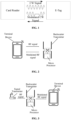
- a mixer is provided in the backscattering device using BPSK modulation. The backscattering device needs to generate a high-frequency signal first, and then use the mixer to modulate the high-frequency signal with the received radio frequency signal to generate a modulated signal, due to the complex structure of the mixer, the structure of the backscatter transmitter is complex and the power consumption is high.
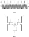
- the control of the keying switch 4 is triggered to continue to control the signal of the receiving antenna 2 and the signal of the transmitting antenna 3 are in the same phase.
- the processor 1 does not trigger the control of the keying switch 4.
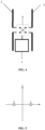
- the backscatter transmitter also includes a first matching network module 5, the first matching network module 5 is located between the receiving antenna 2 and the keying switch 4, and the first matching network module 5 is connected to the receiving antenna 2 and the keying switch 4, respectively.
- the principle of the second matching network module 6 is similar to that of the first matching network module, and description will not be repeated here.
- the first radio frequency signal has a sinusoidal waveform, so the first radio frequency signal is an AC signal, if the radio frequency energy of the first radio frequency signal needs to be converted into electric energy, the integrated energy harvesting device 7 needs to be configured to convert the AC signal into DC signal, and then the energy of the DC signal can be obtained as electric energy.
- the integrated energy harvesting device 7 includes a rectifier 701 and an energy storage 702, and the rectifier 701 is connected to the receiving antenna 2 and the energy storage 702 respectively.
- the first radio frequency signal is a CW signal.
Landscapes
- Engineering & Computer Science (AREA)
- Computer Networks & Wireless Communication (AREA)
- Signal Processing (AREA)
- Microelectronics & Electronic Packaging (AREA)
- Computer Hardware Design (AREA)
- Physics & Mathematics (AREA)
- General Physics & Mathematics (AREA)
- Theoretical Computer Science (AREA)
- Power Engineering (AREA)
- Near-Field Transmission Systems (AREA)
- Transmitters (AREA)
Applications Claiming Priority (1)
| Application Number | Priority Date | Filing Date | Title |
|---|---|---|---|
| PCT/CN2020/094449 WO2021243661A1 (zh) | 2020-06-04 | 2020-06-04 | 反向散射发射机及信号发射方法 |
Publications (2)
| Publication Number | Publication Date |
|---|---|
| EP4156533A1 true EP4156533A1 (de) | 2023-03-29 |
| EP4156533A4 EP4156533A4 (de) | 2023-07-26 |
Family
ID=78831579
Family Applications (1)
| Application Number | Title | Priority Date | Filing Date |
|---|---|---|---|
| EP20939151.5A Withdrawn EP4156533A4 (de) | 2020-06-04 | 2020-06-04 | Rückstreuungssender und signalübertragungsverfahren |
Country Status (4)
| Country | Link |
|---|---|
| US (1) | US20230097295A1 (de) |
| EP (1) | EP4156533A4 (de) |
| CN (1) | CN115668788A (de) |
| WO (1) | WO2021243661A1 (de) |
Families Citing this family (4)
| Publication number | Priority date | Publication date | Assignee | Title |
|---|---|---|---|---|
| US20240296305A1 (en) * | 2020-12-14 | 2024-09-05 | Funai Electric Co., Ltd. | Passively powered iot devices |
| US12137412B2 (en) * | 2022-09-23 | 2024-11-05 | Qualcomm Incorporated | Power consumption model for energy harvesting nodes |
| US12395232B2 (en) | 2023-05-12 | 2025-08-19 | Cisco Technology, Inc. | Backscatter device placement and placement calibration |
| WO2025166828A1 (en) * | 2024-02-09 | 2025-08-14 | Google Llc | Carrier wave and energy management for a wireless device |
Family Cites Families (6)
| Publication number | Priority date | Publication date | Assignee | Title |
|---|---|---|---|---|
| US7904032B2 (en) * | 2006-12-20 | 2011-03-08 | Ncr Corporation | Methods and apparatus for single sideband modulation employing a frequency shift |
| CN102073834A (zh) * | 2009-11-20 | 2011-05-25 | 数伦计算机技术(上海)有限公司 | 射频标识系统 |
| WO2011094750A1 (en) * | 2010-02-01 | 2011-08-04 | Georgia Tech Research Corporation | Multi-antenna signaling scheme for low-powered or passive radio communications |
| CN105981294B (zh) * | 2014-02-10 | 2019-04-26 | 克莱尔瓦扬技术有限公司 | 用于rfid阅读器的极性发射机 |
| US11108435B2 (en) * | 2015-06-03 | 2021-08-31 | Apple Inc. | Inductive power receiver |
| CN106549692B (zh) * | 2016-12-12 | 2019-06-04 | 电子科技大学 | 一种用于反向散射通信系统的信号接收方法 |
-
2020
- 2020-06-04 EP EP20939151.5A patent/EP4156533A4/de not_active Withdrawn
- 2020-06-04 WO PCT/CN2020/094449 patent/WO2021243661A1/zh not_active Ceased
- 2020-06-04 CN CN202080101210.3A patent/CN115668788A/zh active Pending
-
2022
- 2022-12-02 US US18/074,414 patent/US20230097295A1/en not_active Abandoned
Also Published As
| Publication number | Publication date |
|---|---|
| WO2021243661A1 (zh) | 2021-12-09 |
| US20230097295A1 (en) | 2023-03-30 |
| EP4156533A4 (de) | 2023-07-26 |
| CN115668788A (zh) | 2023-01-31 |
Similar Documents
| Publication | Publication Date | Title |
|---|---|---|
| US20230097295A1 (en) | Backscatter transmitter and signal transmission method | |
| US11011941B2 (en) | Method and apparatus for wireless power delivery tracking | |
| US9349029B2 (en) | Transmission apparatus for a wireless device | |
| JP5999693B2 (ja) | レクテナ | |
| US12452097B2 (en) | Signal transmission using backscatter device in wireless communication | |
| CN111066257B (zh) | 用于通过反向散射生成波束成形信号的通信节点和方法 | |
| KR20170081809A (ko) | Rfid 태그 및 그 제어방법 | |
| US9178731B2 (en) | Transmission apparatus for a wireless device using delta-sigma modulation | |
| EP2850735A1 (de) | Vorrichtung zur erzeugung dedizierter datenkanäle in einem rückstrahlungs-rfid-system mit einem tiefpass delta sigma-modulator | |
| US10867137B2 (en) | Passive sensor system powered by wireless energy transmission | |
| US10419254B2 (en) | Transmission apparatus for a wireless device using delta-sigma modulation | |
| Correia et al. | Design of high order modulation backscatter wireless sensor for passive IoT solutions | |
| US7221908B2 (en) | Radio communication apparatus | |
| US20080274697A1 (en) | Radio communication apparatus | |
| US20160371515A1 (en) | Apparatus and method for transmitting and receiving rf signal using beamforming | |
| EP4543139A1 (de) | Kommunikationsvorrichtung und -vorrichtung | |
| KR20200099903A (ko) | 무선 전력 전송 디바이스 및 그 제어 방법 | |
| CN102957649B (zh) | 副载波调制方法 | |
| US20050054299A1 (en) | Silent communicator | |
| CN118232978A (zh) | 信号处理方法、装置、通信设备及存储介质 |
Legal Events
| Date | Code | Title | Description |
|---|---|---|---|
| STAA | Information on the status of an ep patent application or granted ep patent |
Free format text: STATUS: THE INTERNATIONAL PUBLICATION HAS BEEN MADE |
|
| PUAI | Public reference made under article 153(3) epc to a published international application that has entered the european phase |
Free format text: ORIGINAL CODE: 0009012 |
|
| STAA | Information on the status of an ep patent application or granted ep patent |
Free format text: STATUS: REQUEST FOR EXAMINATION WAS MADE |
|
| 17P | Request for examination filed |
Effective date: 20221221 |
|
| AK | Designated contracting states |
Kind code of ref document: A1 Designated state(s): AL AT BE BG CH CY CZ DE DK EE ES FI FR GB GR HR HU IE IS IT LI LT LU LV MC MK MT NL NO PL PT RO RS SE SI SK SM TR |
|
| A4 | Supplementary search report drawn up and despatched |
Effective date: 20230626 |
|
| RIC1 | Information provided on ipc code assigned before grant |
Ipc: H01Q 3/38 20060101ALI20230620BHEP Ipc: H01Q 1/22 20060101ALI20230620BHEP Ipc: G06K 19/077 20060101ALI20230620BHEP Ipc: H04B 5/00 20060101AFI20230620BHEP |
|
| DAV | Request for validation of the european patent (deleted) | ||
| DAX | Request for extension of the european patent (deleted) | ||
| STAA | Information on the status of an ep patent application or granted ep patent |
Free format text: STATUS: THE APPLICATION IS DEEMED TO BE WITHDRAWN |
|
| 18D | Application deemed to be withdrawn |
Effective date: 20240124 |