EP4156533A1 - Backscatter transmitter and signal transmission method - Google Patents
Backscatter transmitter and signal transmission method Download PDFInfo
- Publication number
- EP4156533A1 EP4156533A1 EP20939151.5A EP20939151A EP4156533A1 EP 4156533 A1 EP4156533 A1 EP 4156533A1 EP 20939151 A EP20939151 A EP 20939151A EP 4156533 A1 EP4156533 A1 EP 4156533A1
- Authority
- EP
- European Patent Office
- Prior art keywords
- radio frequency
- frequency signal
- contact point
- antenna
- receiving antenna
- Prior art date
- Legal status (The legal status is an assumption and is not a legal conclusion. Google has not performed a legal analysis and makes no representation as to the accuracy of the status listed.)
- Withdrawn
Links
Images


Classifications
-
- H—ELECTRICITY
- H04—ELECTRIC COMMUNICATION TECHNIQUE
- H04L—TRANSMISSION OF DIGITAL INFORMATION, e.g. TELEGRAPHIC COMMUNICATION
- H04L27/00—Modulated-carrier systems
- H04L27/18—Phase-modulated carrier systems, i.e. using phase-shift keying
- H04L27/20—Modulator circuits; Transmitter circuits
-
- G—PHYSICS
- G06—COMPUTING OR CALCULATING; COUNTING
- G06K—GRAPHICAL DATA READING; PRESENTATION OF DATA; RECORD CARRIERS; HANDLING RECORD CARRIERS
- G06K19/00—Record carriers for use with machines and with at least a part designed to carry digital markings
- G06K19/06—Record carriers for use with machines and with at least a part designed to carry digital markings characterised by the kind of the digital marking, e.g. shape, nature, code
- G06K19/067—Record carriers with conductive marks, printed circuits or semiconductor circuit elements, e.g. credit or identity cards also with resonating or responding marks without active components
- G06K19/07—Record carriers with conductive marks, printed circuits or semiconductor circuit elements, e.g. credit or identity cards also with resonating or responding marks without active components with integrated circuit chips
- G06K19/077—Constructional details, e.g. mounting of circuits in the carrier
- G06K19/07749—Constructional details, e.g. mounting of circuits in the carrier the record carrier being capable of non-contact communication, e.g. constructional details of the antenna of a non-contact smart card
- G06K19/0775—Constructional details, e.g. mounting of circuits in the carrier the record carrier being capable of non-contact communication, e.g. constructional details of the antenna of a non-contact smart card arrangements for connecting the integrated circuit to the antenna
- G06K19/07754—Constructional details, e.g. mounting of circuits in the carrier the record carrier being capable of non-contact communication, e.g. constructional details of the antenna of a non-contact smart card arrangements for connecting the integrated circuit to the antenna the connection being galvanic
-
- H—ELECTRICITY
- H02—GENERATION; CONVERSION OR DISTRIBUTION OF ELECTRIC POWER
- H02J—ELECTRIC POWER NETWORKS; CIRCUIT ARRANGEMENTS OR SYSTEMS FOR SUPPLYING OR DISTRIBUTING ELECTRIC POWER; SYSTEMS FOR STORING ELECTRIC ENERGY
- H02J50/00—Circuit arrangements or systems for wireless supply or distribution of electric power
- H02J50/001—Energy harvesting or scavenging
-
- H—ELECTRICITY
- H04—ELECTRIC COMMUNICATION TECHNIQUE
- H04B—TRANSMISSION
- H04B1/00—Details of transmission systems, not covered by a single one of groups H04B3/00 - H04B13/00; Details of transmission systems not characterised by the medium used for transmission
- H04B1/02—Transmitters
- H04B1/04—Circuits
-
- H—ELECTRICITY
- H04—ELECTRIC COMMUNICATION TECHNIQUE
- H04B—TRANSMISSION
- H04B5/00—Near-field transmission systems, e.g. inductive or capacitive transmission systems
- H04B5/40—Near-field transmission systems, e.g. inductive or capacitive transmission systems characterised by components specially adapted for near-field transmission
- H04B5/45—Transponders
-
- H—ELECTRICITY
- H01—ELECTRIC ELEMENTS
- H01Q—ANTENNAS, i.e. RADIO AERIALS
- H01Q9/00—Electrically-short antennas having dimensions not more than twice the operating wavelength and consisting of conductive active radiating elements
- H01Q9/04—Resonant antennas
- H01Q9/0407—Substantially flat resonant element parallel to ground plane, e.g. patch antenna
-
- H—ELECTRICITY
- H01—ELECTRIC ELEMENTS
- H01Q—ANTENNAS, i.e. RADIO AERIALS
- H01Q9/00—Electrically-short antennas having dimensions not more than twice the operating wavelength and consisting of conductive active radiating elements
- H01Q9/04—Resonant antennas
- H01Q9/16—Resonant antennas with feed intermediate between the extremities of the antenna, e.g. centre-fed dipole
-
- H—ELECTRICITY
- H02—GENERATION; CONVERSION OR DISTRIBUTION OF ELECTRIC POWER
- H02J—ELECTRIC POWER NETWORKS; CIRCUIT ARRANGEMENTS OR SYSTEMS FOR SUPPLYING OR DISTRIBUTING ELECTRIC POWER; SYSTEMS FOR STORING ELECTRIC ENERGY
- H02J50/00—Circuit arrangements or systems for wireless supply or distribution of electric power
- H02J50/20—Circuit arrangements or systems for wireless supply or distribution of electric power using microwaves or radio frequency waves
-
- H—ELECTRICITY
- H04—ELECTRIC COMMUNICATION TECHNIQUE
- H04B—TRANSMISSION
- H04B5/00—Near-field transmission systems, e.g. inductive or capacitive transmission systems
- H04B5/20—Near-field transmission systems, e.g. inductive or capacitive transmission systems characterised by the transmission technique; characterised by the transmission medium
Definitions
- signal modulation methods mainly include three modulation methods of ASK (Amplitude Shift Keying), FSK (Frequency Shift Keying), and PSK (Phase Shift Keying), and a main modulation method in PSK is to use a mixer to realize BPSK (Binary Phase shift keying) modulation.
- a mixer is provided in the backscattering device using BPSK modulation. The backscattering device needs to generate a high-frequency signal first, and then use the mixer to modulate the high-frequency signal with the received radio frequency signal to generate a modulated signal, due to the complex structure of the mixer, the structure of the backscatter transmitter is complex and the power consumption is high.
- the control of the keying switch 4 is triggered to continue to control the signal of the receiving antenna 2 and the signal of the transmitting antenna 3 are in the same phase.
- the processor 1 does not trigger the control of the keying switch 4.
- the backscatter transmitter also includes a first matching network module 5, the first matching network module 5 is located between the receiving antenna 2 and the keying switch 4, and the first matching network module 5 is connected to the receiving antenna 2 and the keying switch 4, respectively.
- the principle of the second matching network module 6 is similar to that of the first matching network module, and description will not be repeated here.
- the first radio frequency signal has a sinusoidal waveform, so the first radio frequency signal is an AC signal, if the radio frequency energy of the first radio frequency signal needs to be converted into electric energy, the integrated energy harvesting device 7 needs to be configured to convert the AC signal into DC signal, and then the energy of the DC signal can be obtained as electric energy.
- the integrated energy harvesting device 7 includes a rectifier 701 and an energy storage 702, and the rectifier 701 is connected to the receiving antenna 2 and the energy storage 702 respectively.
- the first radio frequency signal is a CW signal.
Landscapes
- Engineering & Computer Science (AREA)
- Computer Networks & Wireless Communication (AREA)
- Signal Processing (AREA)
- Microelectronics & Electronic Packaging (AREA)
- Computer Hardware Design (AREA)
- Physics & Mathematics (AREA)
- General Physics & Mathematics (AREA)
- Theoretical Computer Science (AREA)
- Power Engineering (AREA)
- Near-Field Transmission Systems (AREA)
- Transmitters (AREA)
Abstract
Description
- The present disclosure relates to the field of mobile communication, in particular to a backscatter transmitter and a signal transmission method.
- Nowadays, the backscattering technology can use the transmitter to generate the transmitted signal by modulating the received signal, and communicate with other devices using the transmitted signal, without actively transmitting signal.
- In related technologies, signal modulation methods mainly include three modulation methods of ASK (Amplitude Shift Keying), FSK (Frequency Shift Keying), and PSK (Phase Shift Keying), and a main modulation method in PSK is to use a mixer to realize BPSK (Binary Phase shift keying) modulation. A mixer is provided in the backscattering device using BPSK modulation. The backscattering device needs to generate a high-frequency signal first, and then use the mixer to modulate the high-frequency signal with the received radio frequency signal to generate a modulated signal, due to the complex structure of the mixer, the structure of the backscatter transmitter is complex and the power consumption is high.
- The embodiment of the present application provides a backscatter transmitter and a signal transmission method. The phase modulation of the radio frequency signal can be realized simply by the connection path between thee receiving antenna and the transmitting antenna without the need of mixer. The structure is simple, the implementation principle is simple, and no excessive power consumption is required. The technical scheme is as follows:
According to one aspect of the present application, a backscatter transmitter is provided, and the backscatter transmitter includes: a processor, a receiving antenna, a transmitting antenna, and a keying switch; - The processor, the receiving antenna, and the transmitting antenna are respectively connected to the keying switch;
- The processor is configured to control the connection path between the receiving antenna and the transmitting antenna by controlling the keying switch;
- The receiving antenna is configured to receive a first radio frequency signal;
- The connection path is configured to modulate a phase of the first radio frequency signal to obtain a second radio frequency signal that is modulated;
- The transmitting antenna is configured to transmit the second radio frequency signal.
- According to one aspect of the present application, a signal transmission method is provided, which is applied to a backscatter transmitter, and the backscatter transmitter includes: a processor, a receiving antenna, a transmitting antenna, and a keying switch; the processor is connected to the key swatch, and the receiving antenna and the transmitting antenna are respectively connected to the keying switch; the method also includes:
- controlling, by the processor, a connection path between the receiving antenna and the transmitting antenna by controlling the keying switch;
- receiving, by the receiving antenna, a first radio frequency signal;
- configuring the connection path to modulate a phase of the first radio frequency signal to obtain a second radio frequency signal that is modulated; and
- transmitting, by the transmitting antenna, the second radio frequency signal.
- The technical solutions provided by the embodiments of the present application at least include the following beneficial effects:
In the novel backscatter transmitter provided by the embodiment of the present application, the backscatter transmitter includes a processor, a receiving antenna, a transmitting antenna, and a keying switch. The processor controls the connection path between the receiving antenna and the transmitting antenna by controlling the keying switch. The receiving antenna receives the first radio frequency signal, and transmits it to the transmitting antenna through the connection path, during the transmission process, the connection path realizes the modulation of the phase of the first radio frequency signal, and obtains the modulated second radio frequency signal. The second radio frequency signal is transmitted by the transmitting antenna. The phase modulation of the radio frequency signal can be realized only through the connection path between the receiving antenna and the transmitting antenna without providing a mixer. The structure is simple, and the realization principle is simple, and excessive power consumption is no longer required. Moreover, the processor can adjust the connection path between the receiving antenna and the transmitting antenna by controlling the keying switch, which has strong flexibility. - In order to more clearly illustrate the technical solutions in the embodiments of the present application, the drawings that need to be used in the description of the embodiments will be briefly introduced below. Obviously, the drawings in the following description are only some embodiments of the present application. For those skilled in the art, other drawings can also be obtained based on these drawings without creative effort.
-
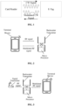
FIG. 1 illustrates a schematic diagram of a backscattering technique provided by an exemplary embodiment of the present application; -
FIG. 2 illustrates schematic diagram of a communication system provided by an exemplary embodiment of the present application; -
FIG. 3 illustrates schematic diagram of a communication system provided by an exemplary embodiment of the present application; -
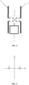
FIG. 4 illustrates schematic structural diagram of a backscatter transmitter provided by an exemplary embodiment of the present application; -
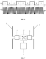
FIG. 5 illustrates a constellation diagram of BPSK provided by an exemplary embodiment of the present application; -
FIG. 6 illustrates a schematic diagram of the relationship between the digital domain and the waveform provided by an exemplary embodiment of the present application; -
FIG. 7 illustrates a schematic structural diagram of a backscatter transmitter provided by an exemplary embodiment of the present application; -
FIG. 8 illustrates a schematic structural diagram of a backscatter transmitter provided by an exemplary embodiment of the present application; -
FIG. 9 illustrates a schematic structural diagram of an integrated energy harvesting device provided by an exemplary embodiment of the present application; -
FIG. 10 illustrates a schematic structural diagram of a backscatter transmitter provided by an exemplary embodiment of the present application; and -
FIG. 11 illustrates a signal transmitting method provided by an exemplary embodiment of the present application. - In order to make the purpose, technical solution and advantages of the present application clearer, the implementation manners of the present application will be further described in detail below in conjunction with the accompanying drawings.
- First, a brief introduction to the terms involved in the embodiments of this application.
- 1. Backscattering technology: it is a wireless technology that realizes signal transmission and encoding without an active transmitter. It also refers to the wireless technology that uses the transmitter to modulate the received signal, and transmit the modulated signal, without actively generating and transmitting signals.
- For example, when the electromagnetic wave reaches the surface of an object, some of the electromagnetic wave will be reflected by the object, and the strength of the reflected signal depends on the shape, material and distance of the object. It can be understood that each object has RCS (Radar Cross Section). In the backscatter system, the electronic tag implements encoding of the signal by changing the RCS, wherein the electronic tag can be the backscatter transmitter in this application.
- The backscatter technique is now illustrated by way of example.
- As shown in
FIG. 1 , the card reader can transmit a CW (Continuous Wave) signal to the electronic tag, and the electronic tag modulates the received CW signal by switching the matching impedance frequency of the antenna to obtain the modulated CW signal, the modulated CW signal is an encoded signal, and the modulated CW signal is transmitted to the card reader to determine the information carried in the modulated CW signal. - Since the electronic tag does not actively generate signals, but only modulates the received signal, the electronic tag realizes the function of the transmitter, thus reducing the power consumption for generating the signal by the transmitter, and the transmitter can absorb the radio frequency energy of the received signal radio, and then converts it into electric energy, so the transmitter does not need to contain a battery, thereby achieving the purpose of zero power consumption.
- In addition,
FIG. 2 illustrates a schematic diagram of a communication system provided by an exemplary embodiment of the present application. Referring toFIG. 2 , the communication system includes a terminal device and a backscatter transmitter. - In this example, the terminal device is integrated with a signal transmitter, and the terminal device can transmit a radio frequency signal through the signal transmitter, and after receiving the radio frequency signal, the backscatter transmitter can modulate the radio frequency signal to obtain a modulated radio frequency signal, and then transmit the modulated radio frequency signal, and the terminal device receives the modulated radio frequency signal.
-
FIG. 3 illustrates schematic diagram of a communication system provided by another exemplary embodiment of the present application. Referring toFIG. 3 , the communication system includes a terminal device, a signal transmitter and a backscatter transmitter. - In this example, the signal transmitter is configured to transmit a radio frequency signal, and after receiving the radio frequency signal, the backscatter transmitter can modulate the radio frequency signal to obtain a modulated radio frequency signal, and then transmit the modulated radio frequency signal, and the terminal device receives the modulated radio frequency signal.
-
FIG. 4 illustrates a schematic structural view of a backscatter transmitter provided by an exemplary embodiment of the present application. Referring toFIG. 4 , the backscatter transmitter includes: aprocessor 1, a receivingantenna 2, a transmittingantenna 3 and a keyingswitch 4. - The backscattering transmitter can adopt the backscattering technology to receive the radio frequency signal, then modulate the radio frequency signal, and transmit the modulated radio frequency signal, and the backscattering transmitter does not need to use a battery, which can save power consumption.
- In a possible implementation, the backscatter transmitter provided by the embodiment of the present application adopts the BPSK modulation mode, and adjusts the phase of the received radio frequency signal so that the phase-adjusted radio frequency signal can represent the code information "0" or code information "1".
- For example,
FIG. 5 is a constellation diagram of BPSK. Refer toFIG. 5 , in the BPSK modulation mode, two signals with the same amplitude and a phase difference of 180 degrees are placed atposition 0 andposition 1. In addition,FIG. 6 is a comparison diagram of digital domain encoding and signal waveforms of BPSK. Referring toFIG. 6 , the low voltage and high voltage in the digital domain represent the code information "0" and "1" respectively, and there are corresponding matching waveforms, and the phase difference between the waveform corresponding to "0" and the waveform corresponding to "1" is 180 degrees. - The backscatter transmitter in the embodiment of the present application can control the phase difference between the signal of the receiving
antenna 2 and the signal of the transmittingantenna 3 by controlling the connection path between the receivingantenna 2 and the transmittingantenna 3. When the radio frequency signal is received by the receivingantenna 2, and then transmitted by the transmittingantenna 3, the phase of the radio frequency signal can be kept unchanged or the phase of the radio frequency signal can be adjusted by 180 degrees. Since the backscatter transmitter provided by the embodiment of the present application can keep the phase of the received radio signal constant or adjust the phase of the radio frequency signal by 180 degrees, when the phase of the radio frequency signal is kept constant, the radio frequency signal transmitted by the transmittingantenna 3 can represent a code "0", and when the phase of the radio frequency signal is adjusted by 180 degrees, the radio frequency signal transmitted by the transmittingantenna 3 can represent a code "1". - In this example, the
processor 1, the receivingantenna 2, and the transmittingantenna 3 in the backscatter transmitter are respectively connected to the keyingswitch 4. - The receiving
antenna 2 is used for receiving the first radio frequency signal. The backscatter transmitter provided in the embodiment of the present application can modulate the first radio frequency signal received by the receivingantenna 2 to obtain a modulated second radio frequency signal. - The first radio frequency signal may be emitted by a card reader, or by a signal transmitter, or by other devices capable of emitting signals.
- In a possible implementation manner, the first radio frequency signal may be a CW radio frequency signal, or a signal of another type. When the first radio frequency signal is a CW radio frequency signal, the CW radio frequency signal is transmitted by a CW transmitter, and the CW transmitter is used to generate a CW radio frequency signal and transmit the CW radio frequency signal.
- The
processor 1 is configured to control the connection path between the receivingantenna 2 and the transmittingantenna 3 by controlling the keyingswitch 4, the connection path can modulate the phase of the first radio frequency signal to obtain a modulated second radio frequency signal, and the transmittingantenna 3 is used to transmit the second radio frequency signal. - In a possible implementation manner, the keying switch controls the positive pole of the receiving
antenna 2 to be connected to the positive pole of the transmittingantenna 3, and the negative pole of the receivingantenna 2 to be connected to the negative pole of the transmitting antenna 3to ensure that the phases are the same. - In another possible implementation, the positive pole of the receiving
antenna 2 is connected to the negative pole of the transmittingantenna 3, and the negative pole of the receivingantenna 2 is connected to the positive pole of the transmittingantenna 3 to ensure a phase difference of 180 degrees. - Before controlling the keying
switch 4, theprocessor 1 first determines the code information represented by the second radio frequency signal to be transmitted. After determining the currently required code information, it can control the keyingswitch 4, and control the connection path between the receivingantenna 2 and the transmitting antenna3, then the receivingantenna 2 can transmit the radio frequency signal carrying the code information. - In a possible implementation, the keying
switch 4 is a double-pole double-throw switch, or other types of switches. - It should be noted that the keying
switch 4 has an initial state. When theprocessor 1 controls the keyingswitch 4 and controls the connection path between the receivingantenna 2 and the transmittingantenna 3, the initial state of thecurrent keying switch 4 is first judged. If thecontrol switch 4 meets the connection path of receivingantenna 2 and transmittingantenna 3, then the state of keyingswitch 4 is not changed, and if the control switch 4does not meet the connection path of receivingantenna 2 and transmittingantenna 3, the keyingswitch 4 is adjusted to another state. - For example, when the information that
processor 1 needs to send is "110011 ", when the first character "1" is transmitted, theprocessor 1 controls the keyingswitch 4, to control that the positive pole of receivingantenna 2 is connected with the positive pole of transmittingantenna 3, and the negative pole of the receivingantenna 2 is connected with the negative pole of the transmittingantenna 3, so that the signal of the receivingantenna 2 and the signal of the transmittingantenna 3 are in the same phase. When the second character "1" is transmitted, theprocessor 1 does not trigger the control of the keying switch 4.When the third character "0" is transmitted, because it is different from the previous character "1", the control of the keyingswitch 4 is triggered to control that the positive pole of the receivingantenna 2 is connected with the negative pole of the transmittingantenna 3, and the negative pole of the receivingantenna 2 is connected with the positive pole of the transmittingantenna 3, so that the signal of the receivingantenna 2 and the signal of the transmittingantenna 3 are in opposite phases. When the fourth character "0" is transmitted, theprocessor 1 does not trigger the control of the keyingswitch 4. When the fifth character "1" is transmitted, because it is different from the previous character "0", the control of the keyingswitch 4 is triggered to continue to control the signal of the receivingantenna 2 and the signal of the transmittingantenna 3 are in the same phase. When the sixth character "1" is transmitted, theprocessor 1 does not trigger the control of the keyingswitch 4. - In a possible implementation manner, the transmitting
antenna 3 in the embodiment of the present application is any one of a patch antenna and a dipole antenna. - In another possible implementation manner, the receiving
antenna 2 in the embodiment of the present application is any one of a patch antenna and a dipole antenna. - It should be noted that, when the transmitting
antenna 3 and the receivingantenna 2 in the embodiment of the present application are both patch antennas, the transmittingantenna 3 and the receivingantenna 2 cannot adopt a common ground structure. - In addition, the backscatter transmitter provided by the embodiment of the present application can be applied in more wireless transmission protocols, for example, it can be applied in Bluetooth technology, or it can be applied in Wi -Fi (Wireless Fidelity) technology, or in the cellular network, or in the RFID (Radio Frequency ID entification) technology and the like.
- In the novel backscatter transmitter provided by the embodiment of the present application, the backscatter transmitter includes a processor, a receiving antenna, a transmitting antenna, and a keying switch. The processor controls the connection patch between the receiving antenna and the transmitting antenna by controlling the keying switch. The receiving antenna receives the first radio frequency signal, and transmits it to the transmitting antenna through the connection patch, during the transmission process, the connection patch realizes the modulation of the phase of the first radio frequency signal, and obtains the modulated second radio frequency signal. The second radio frequency signal is transmitted by the transmitting antenna. The phase modulation of the radio frequency signal can be realized only through the connection path between the receiving antenna and the transmitting antenna without providing a mixer. The structure is simple, and the realization principle is simple, and excessive power consumption is no longer required. Moreover, the processor can adjust the connection path between the receiving antenna and the transmitting antenna by controlling the keying switch, which has strong flexibility.
- In a possible implementation, the backscatter transmitter also includes a first
matching network module 5, the firstmatching network module 5 is located between the receivingantenna 2 and the keyingswitch 4, and the firstmatching network module 5 is connected to the receivingantenna 2 and the keyingswitch 4, respectively. - In this example, the first
matching network module 5 is configured to adjust the impedance of the first radio frequency signal, so that the adjusted impedance of the first radio frequency signal matches the impedance of the keyingswitch 4. - In the embodiment of the present application, since the receiving
antenna 2 and the keyingswitch 4 in the backscatter transmitter both have impedances, if the impedances of the receivingantenna 2 and the keyingswitch 4 are different, when the first radio frequency received by the receiving antenna reaches the keyingswitch 4, it will cause the attenuation of the first radio frequency signal, and the maximum energy efficiency cannot be achieved. Therefore, between the receivingantenna 2 and the keyingswitch 4, a firstmatching network module 5 is provided. The firstmatching network module 5 is used to adjust the impedance of the first radio frequency signal, so that the adjusted impedance of the first radio frequency signal matches the impedance of the keyingswitch 4 to ensure the transmission of the radio frequency signal. - Moreover, after the first
matching network module 5 is provided between the receivingantenna 2 and the keyingswitch 4, the connection path between the receivingantenna 2 and the transmittingantenna 3 includes the firstmatching network module 5 and the keyingswitch 4. - In another possible implementation, the backscatter transmitter further includes a second
matching network module 6, the secondmatching network module 6 is located between the transmittingantenna 3 and the keyingswitch 4, and the secondmatching network module 6 is connected with transmittingantenna 3 and the keyingswitch 4, respectively. - The second
matching network module 6 is configured to adjust the impedance of the second radio frequency signal, so that the adjusted impedance of the second radio frequency signal matches the impedance of the transmittingantenna 3. - In this example, the principle of the second
matching network module 6 is similar to that of the first matching network module, and description will not be repeated here. - Moreover, after the second
matching network module 6 is provided between the receivingantenna 2 and the keyingswitch 4, the connection path between the receivingantenna 2 and the transmittingantenna 3 includes the secondmatching network module 6 and the keyingswitch 4. - For example, as shown in
FIG. 7 , a firstmatching network module 5 is provided between the receivingantenna 2 and the keyingswitch 4, and a secondmatching network module 6 is provided between the keyingswitch 4 and the transmittingantenna 3. The backscatter transmitter in the embodiment can use the firstmatching network module 5 and the secondmatching network module 6 to adjust the first radio frequency signal and the second radio frequency signal respectively, so that the impedance of the adjusted radio frequency signal match. It should be noted that after the firstmatching network module 5 is provided between the receivingantenna 2 and the keyingswitch 4, and the secondmatching network module 6 is provided between the keyingswitch 4 and the transmittingantenna 3, the connection path between the receivingantenna 2 and the transmittingantennas 3 includes the firstmatching network module 5, the secondmatching network module 6 and the keyingswitch 4. - The backscatter transmitter provided in the embodiment of the present application can adjust the impedance of the radio frequency signal in the backscatter transmitter by providing the first matching network module and the second matching network module, so as to ensure that the radio frequency signal reaches the maximum power transmission, improving the performance of backscatter transmitters.
- In another possible implementation manner, as shown in
FIG. 8 , the backscatter transmitter further includes an integratedenergy harvesting device 7, and the integratedenergy harvesting device 7 is connected to the receivingantenna 2. - In this example, the integrated
energy harvesting device 7 is configured to receive the radio frequency energy of the first radio frequency signal, convert the radio frequency energy into electric energy and store it. - After the receiving
antenna 2 receives the first radio frequency signal, the first radio frequency signal contains radio frequency energy, thus the radio frequency energy of the first radio frequency signal can be converted into electric energy through the provided integratedenergy harvesting device 7. - In this example, the first radio frequency signal has a sinusoidal waveform, so the first radio frequency signal is an AC signal, if the radio frequency energy of the first radio frequency signal needs to be converted into electric energy, the integrated
energy harvesting device 7 needs to be configured to convert the AC signal into DC signal, and then the energy of the DC signal can be obtained as electric energy. - Optionally, as shown in
FIG. 9 , the integratedenergy harvesting device 7 includes arectifier 701 and anenergy storage 702, and therectifier 701 is connected to the receivingantenna 2 and theenergy storage 702 respectively. - In this example, the
rectifier 701 is used to receive the radio frequency energy of the first radio frequency signal, and convert the radio frequency energy into electric energy. Then the electric energy is sent to theenergy storage 702, and theenergy storage 702 stores the electric energy. - The
rectifier 701 can rectify the received signal, and can also boost the voltage of the rectified signal, so that the subsequent process can obtain a signal that meets the requirements, and then obtain the power. - In this example, the
rectifier 701 may be a voltage multiplier, or other devices. - The integrated energy harvesting device provided in the embodiment of the present application can convert the radio frequency energy of the first radio frequency signal into electric energy and store the electric energy, so the backscatter transmitter can use the electric energy stored in the integrated energy harvesting device without providing a battery for the backscatter transmitter, thereby saving power consumption and improving energy utilization.
- In another possible implementation, as shown in
FIG. 10 , the keyingswitch 4 includes afirst contact point 401, asecond contact point 402, athird contact point 403, and afourth contact point 404. Thefirst contact point 401 and thesecond contact point 402 are all located on the receivingantenna 2, thethird contact point 403 and thefourth contact point 404 are all located on the transmittingantenna 3. Thefirst contact point 401 and thethird contact point 403 are positive poles, and thesecond contact point 402 and thefourth contact point 404 are negative poles. - The keying
switch 4 is configured to connect thefirst contact point 401 and thethird contact point 403, and connect thesecond contact point 402 and thefourth contact point 404 to form a connection path between the receivingantenna 2 and the transmittingantenna 3. In this case, the positive pole of receivingantenna 2 is connected with the positive pole of transmittingantenna 3, and the negative pole of receivingantenna 2 is connected with the negative pole of transmittingantenna 3. In this case, the receivingantenna 2 is in the same phase with transmittingantenna 3. After receivingantenna 2 receives the first radio frequency signal, it is transmitted to the transmitting antenna through the connection path. During the transmission process, the modulation of the first radio frequency signal is realized, and the second radio frequency signal transmitted by the transmittingantenna 3 is in the same phase with the first radio frequency signal. - Alternatively, the keying switch4 is configured to connect the
first contact point 401 to thefourth contact point 404, connect thesecond contact point 402 to thethird contact point 403, and form a connection path between the receivingantenna 2 and the transmittingantenna 3. In this case, the positive pole of the receivingantenna 2 is connected to the negative pole of the transmittingantenna 3, and the negative pole of the receivingantenna 2 is connected to the positive pole of the transmittingantenna 3. In this case, the receivingantenna 2 and the transmittingantenna 3 are in opposite phases, and after the receivingantenna 2 receives the first radio frequency signal, it is transmitted to the transmitting antenna through the connection path. During the transmission process, the modulation of the first radio frequency signal is realized, and the second radio frequency signal transmitted by the transmittingantenna 3 is in the opposite phase to the first radio frequency signal. - Through the above method, when the
processor 1 determines that the second radio frequency signal to be transmitted is in the same phase with the first radio frequency signal, theprocessor 1 controls the keyingswitch 4 to connect thefirst contact point 401 to thethird contact point 403, and connect thesecond contact point 402 to thefourth contact point 404, so the first radio frequency signal of the transmittingantenna 3 and the second radio frequency signal of the receivingantenna 2 have the same phase. - When the
processor 1 determines that the second radio frequency signal to be transmitted is in the opposite phase to the first radio frequency signal, theprocessor 1 controls the keyingswitch 4 to connect thefirst contact point 401 to thefourth contact point 404, and thesecond contact point 402 to thethird contact point 403, so the first radio frequency signal of the transmittingantenna 3 and the second radio frequency signal of the receivingantenna 2 are in opposite phases. - In the backscatter transmitter provided by the embodiment of the present application, the keying switch includes a first contact point, a second contact point, a third contact point and a fourth contact point. Both the first contact point and the second contact point are located at the receiving antenna, and both the third contact point and the fourth contact point are located on the transmitting antenna. The first contact point and the third contact point are positive poles, and the second contact point and the fourth contact point are negative poles. The positive poles and the negative poles of the receiving antenna and the transmitting antenna can be adjusted by the keying switch. By adjusting the connection path between the positive and negative poles of the receiving antenna and the transmitting antenna, the RF signal of the receiving antenna and the RF signal of the transmitting antenna can be in the same phase or different phases, that is, modulation of the radio frequency signal is realized, and then the backscattering technology is realized.
-
FIG. 11 is a flow chart of a signal transmission method provided by an exemplary embodiment of the present application. Referring toFIG. 11 , it is applied to a backscatter transmitter, and the backscatter transmitter includes: a processor, a receiving antenna, a transmitting antenna and a keying switch; the processor is connected to the keying switch, and the receiving antenna and the transmitting antenna are respectively connected to the keying switch; the method also includes: -
Step 1111. The processor controls the connection path between the receiving antenna and the transmitting antenna by controlling the keying switch. -
Step 1121. The receiving antenna receives the first radio frequency signal. -
Step 1131. The connection path modulates the phase of the first radio frequency signal to obtain a modulated second radio frequency signal. -
Step 1141. The transmitting antenna transmits the second radio frequency signal. - The method provided in the embodiment of the present application is applied to a backscatter transmitter. The backscatter transmitter includes a processor, a receiving antenna, a transmitting antenna, and a keying switch to control the connection path between the receiving antenna and the transmitting antenna. The antenna receives the first radio frequency signal, and transmits it to the transmitting antenna through the connection path. During the transmission process, the connection path realizes the phase modulation of the first radio frequency signal, and obtains the modulated second radio frequency signal, which is transmitted by the transmitting antenna. The phase modulation of the radio frequency signal can be realized only through the connection path between the receiving antenna and the transmitting antenna without providing a mixer. The structure is simple, and the realization principle is simple, and excessive power consumption is no longer required. Moreover, the processor can adjust the connection path between the receiving antenna and the transmitting antenna by controlling the keying switch, which has strong flexibility.
- In a possible implementation manner, the backscatter transmitter further includes a first matching network module; the first matching network module is located between the receiving antenna and the keying switch, and the first matching network module is connected to the receiving antenna and the keying switch respectively. The method also includes:
The first matching network module adjusts the impedance of the first radio frequency signal, so that the adjusted impedance of the first radio frequency signal matches the impedance of the keying switch. - In another possible implementation, the backscatter transmitter further includes a second matching network module; the second matching network module is located between the transmitting antenna and the keying switch, and the second matching network module is connected to the transmitting antenna and the keying switch respectively. The method also includes:
The second matching network module adjusts the impedance of the second radio frequency signal, so that the adjusted impedance of the second radio frequency signal matches the impedance of the transmitting antenna. - In another possible implementation, the backscatter transmitter also includes an integrated energy harvesting device; the integrated energy harvesting device is connected to the receiving antenna; and the method also includes:
- The integrated energy harvesting device receives the radio frequency energy of the first radio frequency signal, converts the radio frequency energy into electric energy and stores it.
- In another possible implementation, the integrated energy harvesting device includes a rectifier and an energy storage; the rectifier is respectively connected to the receiving antenna and the energy storage; the integrated energy harvesting device receives the radio frequency energy of the first radio frequency signal, converts the radio frequency energy into electric energy and stores it, which includes:
The rectifier receives the radio frequency energy of the first radio frequency signal, and converts the radio frequency energy into electric energy; - The energy storage stores the electric energy.
- In another possible implementation manner, the keying switch includes a first contact point, a second contact point, a third contact point, and a fourth contact point; both the first contact point and the second contact point are located on the receiving antenna, and both the third contact point and the fourth contact point are located on the transmitting antenna, the first contact point and the third contact point are positive poles, and the second contact point and the fourth contact point are negative poles. The method also includes:
- The processor controls the keying switch to connect the first contact point with the third contact point and connect the second contact point with the fourth contact point to form a connection path, and the first radio frequency signal of the transmitting antenna and the second radio frequency signal of the receiving antenna are in the same phase.
- When the processor controls the keying switch to connect the first contact point with the fourth contact point and connect the second contact point with the third contact point to form the connection path, the first radio frequency signal of the transmitting antenna and the second radio frequency signal of the receiving antenna are in opposite phase.
- In another possible implementation manner, the transmitting antenna is any one of a patch antenna and a dipole antenna.
- In another possible implementation manner, the receiving antenna is any one of a patch antenna and a dipole antenna.
- In another possible implementation manner, the first radio frequency signal is a CW signal.
- Those of ordinary skill in the art can understand that all or part of the steps of the above embodiments can be implemented by hardware, and can also be implemented by instructing related hardware through a program. The program can be stored in a computer-readable storage medium. The above-mentioned storage medium mentioned may be a read-only memory, a magnetic disk or an optical disk, and the like.
- The above are only optional embodiments of the application, and are not intended to limit the application. Any modifications, equivalent replacements, improvements, etc. made within the spirit and principles of the application shall be included in the protection scope of the application.
Claims (18)
- A backscatter transmitter, wherein the backscatter transmitter comprises: a processor (1), a receiving antenna (2), a transmitting antenna (3) and a keying switch (4);the processor (1), the receiving antenna (2), and the transmitting antenna (3) are respectively connected to the keying switch (4);the processor (1) is configured to control a connection path between the receiving antenna (2) and the transmitting antenna (3) by controlling the keying switch (4);the receiving antenna (2) is configured to receive a first radio frequency signal;the connection path is configured to modulate a phase of the first radio frequency signal to obtain a modulated second radio frequency signal; andthe transmitting antenna (3) is configured to transmit the second radio frequency signal.
- The backscatter transmitter according to claim 1, wherein the backscatter transmitter further comprises a first matching network module (5);the first matching network module (5) is disposed between the receiving antenna (2) and the keying switch (4), and the first matching network module (5) is connected to the receiving antenna (2) and the keying switch (4); andthe first matching network module (5) is configured to adjust an impedance of the first radio frequency signal, to match an adjusted impedance of the first radio frequency signal and an impedance of the keying switch (4).
- The backscatter transmitter according to claim 1, wherein the backscatter transmitter further comprises a second matching network module (6);the second matching network module (6) is disposed between the transmitting antenna (3) and the keying switch (4), and the second matching network module (6) is connected to the transmitting antenna (3) and the keying switch (4); andthe second matching network module (6) is configured to adjust an impedance of the second radio frequency signal, to match an adjusted impedance of the second radio frequency signal and an impedance of the transmitting antenna (3).
- The backscatter transmitter according to claim 1, wherein the backscatter transmitter further comprises an integrated energy harvesting device (7);the integrated energy harvesting device (7) is connected to the receiving antenna (2); andthe integrated energy harvesting device (7) is configured to receive radio frequency energy of the first radio frequency signal, convert the radio frequency energy into electric energy and store the electric energy.
- The backscatter transmitter according to claim 4, wherein the integrated energy harvesting device (7) comprises a rectifier (701) and an energy storage (702);the rectifier (701) is respectively connected to the receiving antenna (2) and the energy storage (702);the rectifier (701) is configured to receive radio frequency energy of the first radio frequency signal, and convert the radio frequency energy into electric energy; andthe energy storage (702) is configured to store the electric energy.
- The backscatter transmitter according to claim 1, wherein the keying switch (4) comprises a first contact point (401), a second contact point (402), a third contact point (403) and a fourth contact point (404);both the first contact point (401) and the second contact point (402) are located on the receiving antenna (2), and both the third contact point (403) and the fourth contact point (404) are located on the transmitting antenna (3), the first contact point (401) and the third contact point (403) are positive poles, the second contact point (402) and the fourth contact point (404) are negative poles;the processor (1) is configured to control the keying switch (4) to connect the first contact point (401) to the third contact point (403) and connect the second contact point (402) to the fourth contact point (404) to form the connection path, and the first radio frequency signal of the transmitting antenna (3) and the second radio frequency signal of the receiving antenna (2) are in same phase; andthe processor (1) is configured to control the keying switch (4) to connect the first contact point (401) to the fourth contact point (404) and connect the second contact point (402) to the third contact point (403) to form the connection path, and the first radio frequency signal of the transmitting antenna (3) and the second radio frequency signal of the receiving antenna (2) are in opposite phases.
- The backscatter transmitter according to any one of claims 1-6, wherein the transmitting antenna (3) is any one of a patch antenna and a dipole antenna.
- The backscatter transmitter according to any one of claims 1-6, wherein that the receiving antenna (2) is any one of a patch antenna and a dipole antenna.
- The backscatter transmitter according to any one of claims 1-6, wherein the first radio frequency signal is a continuous wave CW signal.
- A signal transmission method, applied to a backscatter transmitter, wherein the backscatter transmitter comprises: a processor, a receiving antenna, a transmitting antenna and a keying switch; the processor is connected to the keying switch, and the receiving antenna and the transmitting antenna are respectively connected to the keying switch; wherein the method comprises:controlling, by the processor, a connection path between the receiving antenna and the transmitting antenna by controlling the keying switch;receiving, by the receiving antenna, a first radio frequency signal;modulating, by the connection path, a phase of the first radio frequency signal to obtain a modulated second radio frequency signal; andtransmitting, by the transmitting antenna, the second radio frequency signal.
- The method according to claim 10, wherein the backscatter transmitter further comprises a first matching network module; the first matching network module is disposed between the receiving antenna and the keying switch, and the first matching network module is respectively connected to the receiving antenna and the keying switch; the method further comprises:
adjusting, by the first matching network module, an impedance of the first radio frequency signal, to match an adjusted impedance of the first radio frequency signal and an impedance of the keying switch. - The method according to claim 10, wherein the backscatter transmitter further comprises a second matching network module; the second matching network module is disposed between the transmitting antenna and the keying switch, and the second matching network module is respectively connected to the transmitting antenna and the keying switch; the method further comprises:
adjusting, by the second matching network module, an impedance of the second radio frequency signal, to match an adjusted impedance of the second radio frequency signal and an impedance of the transmitting antenna. - The method according to claim 10, wherein the backscatter transmitter further comprises an integrated energy harvesting device; the integrated energy harvesting device is connected to the receiving antenna; the method further comprises:
receiving, by the integrated energy harvesting device, radio frequency energy of the first radio frequency signal, converting the radio frequency energy into electric energy and storing the electric energy. - The method according to claim 11, wherein the integrated energy harvesting device comprises a rectifier and an energy storage; the rectifier is respectively connected to the receiving antenna and the energy storage; and receiving, by the integrated energy harvesting device, radio frequency energy of the first radio frequency signal, converting the radio frequency energy into electric energy and storing the electric energy comprising:receiving, by the rectifier, radio frequency energy of the first radio frequency signal, and converting the radio frequency energy into electric energy; andstoring, by the energy storage, the electric energy.
- The method according to claim 9, wherein the keying switch comprises a first contact point, a second contact point, a third contact point and a fourth contact point; both the first contact point and the second contact points are located on the receiving antenna, both the third contact point and the fourth contact point are located on the transmitting antenna, the first contact point and the third contact point are positive poles, and the second contact point and the fourth contact point are negative poles; the method further comprises:controlling, by the processor, the keying switch to connect the first contact point with the third contact point, and connect the second contact point with the fourth contact point to form the connection path, and the first radio frequency signal of the transmitting antenna and the second radio frequency signal of the receiving antenna are in same phase; andcontrolling, by the processor, the keying switch to connect the first contact point with the fourth contact point, and connect the second contact point with the third contact point to form the connection path, and the first radio frequency signal of the transmitting antenna and the second radio frequency signal of the receiving antenna are in opposite phases.
- The method according to any one of claims 10-15, wherein the transmitting antenna is any one of a patch antenna and a dipole antenna.
- The method according to any one of claims 10-15, wherein the receiving antenna is any one of a patch antenna and a dipole antenna.
- The method according to any one of claims 10-15, wherein the first radio frequency signal is a continuous wave CW signal.
Applications Claiming Priority (1)
| Application Number | Priority Date | Filing Date | Title |
|---|---|---|---|
| PCT/CN2020/094449 WO2021243661A1 (en) | 2020-06-04 | 2020-06-04 | Backscatter transmitter and signal transmission method |
Publications (2)
| Publication Number | Publication Date |
|---|---|
| EP4156533A1 true EP4156533A1 (en) | 2023-03-29 |
| EP4156533A4 EP4156533A4 (en) | 2023-07-26 |
Family
ID=78831579
Family Applications (1)
| Application Number | Title | Priority Date | Filing Date |
|---|---|---|---|
| EP20939151.5A Withdrawn EP4156533A4 (en) | 2020-06-04 | 2020-06-04 | BACK SCATTER TRANSMITTERS AND SIGNAL TRANSMISSION METHODS |
Country Status (4)
| Country | Link |
|---|---|
| US (1) | US20230097295A1 (en) |
| EP (1) | EP4156533A4 (en) |
| CN (1) | CN115668788A (en) |
| WO (1) | WO2021243661A1 (en) |
Families Citing this family (4)
| Publication number | Priority date | Publication date | Assignee | Title |
|---|---|---|---|---|
| US20240296305A1 (en) * | 2020-12-14 | 2024-09-05 | Funai Electric Co., Ltd. | Passively powered iot devices |
| US12137412B2 (en) * | 2022-09-23 | 2024-11-05 | Qualcomm Incorporated | Power consumption model for energy harvesting nodes |
| US12395232B2 (en) | 2023-05-12 | 2025-08-19 | Cisco Technology, Inc. | Backscatter device placement and placement calibration |
| WO2025166828A1 (en) * | 2024-02-09 | 2025-08-14 | Google Llc | Carrier wave and energy management for a wireless device |
Family Cites Families (6)
| Publication number | Priority date | Publication date | Assignee | Title |
|---|---|---|---|---|
| US7904032B2 (en) * | 2006-12-20 | 2011-03-08 | Ncr Corporation | Methods and apparatus for single sideband modulation employing a frequency shift |
| CN102073834A (en) * | 2009-11-20 | 2011-05-25 | 数伦计算机技术(上海)有限公司 | Radio frequency identification system |
| WO2011094750A1 (en) * | 2010-02-01 | 2011-08-04 | Georgia Tech Research Corporation | Multi-antenna signaling scheme for low-powered or passive radio communications |
| CN105981294B (en) * | 2014-02-10 | 2019-04-26 | 克莱尔瓦扬技术有限公司 | Polar Transmitter for RFID Reader |
| US11108435B2 (en) * | 2015-06-03 | 2021-08-31 | Apple Inc. | Inductive power receiver |
| CN106549692B (en) * | 2016-12-12 | 2019-06-04 | 电子科技大学 | A signal receiving method for a backscatter communication system |
-
2020
- 2020-06-04 EP EP20939151.5A patent/EP4156533A4/en not_active Withdrawn
- 2020-06-04 WO PCT/CN2020/094449 patent/WO2021243661A1/en not_active Ceased
- 2020-06-04 CN CN202080101210.3A patent/CN115668788A/en active Pending
-
2022
- 2022-12-02 US US18/074,414 patent/US20230097295A1/en not_active Abandoned
Also Published As
| Publication number | Publication date |
|---|---|
| WO2021243661A1 (en) | 2021-12-09 |
| US20230097295A1 (en) | 2023-03-30 |
| EP4156533A4 (en) | 2023-07-26 |
| CN115668788A (en) | 2023-01-31 |
Similar Documents
| Publication | Publication Date | Title |
|---|---|---|
| US20230097295A1 (en) | Backscatter transmitter and signal transmission method | |
| US11011941B2 (en) | Method and apparatus for wireless power delivery tracking | |
| US9349029B2 (en) | Transmission apparatus for a wireless device | |
| JP5999693B2 (en) | Rectena | |
| US12452097B2 (en) | Signal transmission using backscatter device in wireless communication | |
| CN111066257B (en) | Communication node and method for generating a beamformed signal through backscatter | |
| KR20170081809A (en) | RFID tag and controlling method | |
| US9178731B2 (en) | Transmission apparatus for a wireless device using delta-sigma modulation | |
| EP2850735A1 (en) | Apparatus for generating dedicated data channels in backscatter rfid system using low pass delta sygma modulator | |
| US10867137B2 (en) | Passive sensor system powered by wireless energy transmission | |
| US10419254B2 (en) | Transmission apparatus for a wireless device using delta-sigma modulation | |
| Correia et al. | Design of high order modulation backscatter wireless sensor for passive IoT solutions | |
| US7221908B2 (en) | Radio communication apparatus | |
| US20080274697A1 (en) | Radio communication apparatus | |
| US20160371515A1 (en) | Apparatus and method for transmitting and receiving rf signal using beamforming | |
| EP4543139A1 (en) | Communication apparatus and device | |
| KR20200099903A (en) | Wireless power transmission device and method the same | |
| CN102957649B (en) | subcarrier modulation method | |
| US20050054299A1 (en) | Silent communicator | |
| CN118232978A (en) | Signal processing method, device, communication equipment and storage medium |
Legal Events
| Date | Code | Title | Description |
|---|---|---|---|
| STAA | Information on the status of an ep patent application or granted ep patent |
Free format text: STATUS: THE INTERNATIONAL PUBLICATION HAS BEEN MADE |
|
| PUAI | Public reference made under article 153(3) epc to a published international application that has entered the european phase |
Free format text: ORIGINAL CODE: 0009012 |
|
| STAA | Information on the status of an ep patent application or granted ep patent |
Free format text: STATUS: REQUEST FOR EXAMINATION WAS MADE |
|
| 17P | Request for examination filed |
Effective date: 20221221 |
|
| AK | Designated contracting states |
Kind code of ref document: A1 Designated state(s): AL AT BE BG CH CY CZ DE DK EE ES FI FR GB GR HR HU IE IS IT LI LT LU LV MC MK MT NL NO PL PT RO RS SE SI SK SM TR |
|
| A4 | Supplementary search report drawn up and despatched |
Effective date: 20230626 |
|
| RIC1 | Information provided on ipc code assigned before grant |
Ipc: H01Q 3/38 20060101ALI20230620BHEP Ipc: H01Q 1/22 20060101ALI20230620BHEP Ipc: G06K 19/077 20060101ALI20230620BHEP Ipc: H04B 5/00 20060101AFI20230620BHEP |
|
| DAV | Request for validation of the european patent (deleted) | ||
| DAX | Request for extension of the european patent (deleted) | ||
| STAA | Information on the status of an ep patent application or granted ep patent |
Free format text: STATUS: THE APPLICATION IS DEEMED TO BE WITHDRAWN |
|
| 18D | Application deemed to be withdrawn |
Effective date: 20240124 |