EP4156505A1 - Oscillator with tapped inductor - Google Patents
Oscillator with tapped inductor Download PDFInfo
- Publication number
- EP4156505A1 EP4156505A1 EP22181127.6A EP22181127A EP4156505A1 EP 4156505 A1 EP4156505 A1 EP 4156505A1 EP 22181127 A EP22181127 A EP 22181127A EP 4156505 A1 EP4156505 A1 EP 4156505A1
- Authority
- EP
- European Patent Office
- Prior art keywords
- inductor
- tap
- terminal
- oscillator
- coupled
- Prior art date
- Legal status (The legal status is an assumption and is not a legal conclusion. Google has not performed a legal analysis and makes no representation as to the accuracy of the status listed.)
- Withdrawn
Links
- 239000003990 capacitor Substances 0.000 claims description 2
- 238000010586 diagram Methods 0.000 description 10
- 230000010355 oscillation Effects 0.000 description 3
- 230000004075 alteration Effects 0.000 description 1
- 230000004907 flux Effects 0.000 description 1
- 238000000034 method Methods 0.000 description 1
- 238000012986 modification Methods 0.000 description 1
- 230000004048 modification Effects 0.000 description 1
Images



Classifications
-
- H—ELECTRICITY
- H03—ELECTRONIC CIRCUITRY
- H03B—GENERATION OF OSCILLATIONS, DIRECTLY OR BY FREQUENCY-CHANGING, BY CIRCUITS EMPLOYING ACTIVE ELEMENTS WHICH OPERATE IN A NON-SWITCHING MANNER; GENERATION OF NOISE BY SUCH CIRCUITS
- H03B5/00—Generation of oscillations using amplifier with regenerative feedback from output to input
- H03B5/08—Generation of oscillations using amplifier with regenerative feedback from output to input with frequency-determining element comprising lumped inductance and capacitance
- H03B5/12—Generation of oscillations using amplifier with regenerative feedback from output to input with frequency-determining element comprising lumped inductance and capacitance active element in amplifier being semiconductor device
- H03B5/1228—Generation of oscillations using amplifier with regenerative feedback from output to input with frequency-determining element comprising lumped inductance and capacitance active element in amplifier being semiconductor device the amplifier comprising one or more field effect transistors
-
- H—ELECTRICITY
- H03—ELECTRONIC CIRCUITRY
- H03B—GENERATION OF OSCILLATIONS, DIRECTLY OR BY FREQUENCY-CHANGING, BY CIRCUITS EMPLOYING ACTIVE ELEMENTS WHICH OPERATE IN A NON-SWITCHING MANNER; GENERATION OF NOISE BY SUCH CIRCUITS
- H03B5/00—Generation of oscillations using amplifier with regenerative feedback from output to input
- H03B5/08—Generation of oscillations using amplifier with regenerative feedback from output to input with frequency-determining element comprising lumped inductance and capacitance
- H03B5/12—Generation of oscillations using amplifier with regenerative feedback from output to input with frequency-determining element comprising lumped inductance and capacitance active element in amplifier being semiconductor device
- H03B5/1206—Generation of oscillations using amplifier with regenerative feedback from output to input with frequency-determining element comprising lumped inductance and capacitance active element in amplifier being semiconductor device using multiple transistors for amplification
- H03B5/1212—Generation of oscillations using amplifier with regenerative feedback from output to input with frequency-determining element comprising lumped inductance and capacitance active element in amplifier being semiconductor device using multiple transistors for amplification the amplifier comprising a pair of transistors, wherein an output terminal of each being connected to an input terminal of the other, e.g. a cross coupled pair
-
- H—ELECTRICITY
- H03—ELECTRONIC CIRCUITRY
- H03B—GENERATION OF OSCILLATIONS, DIRECTLY OR BY FREQUENCY-CHANGING, BY CIRCUITS EMPLOYING ACTIVE ELEMENTS WHICH OPERATE IN A NON-SWITCHING MANNER; GENERATION OF NOISE BY SUCH CIRCUITS
- H03B5/00—Generation of oscillations using amplifier with regenerative feedback from output to input
- H03B5/08—Generation of oscillations using amplifier with regenerative feedback from output to input with frequency-determining element comprising lumped inductance and capacitance
- H03B5/12—Generation of oscillations using amplifier with regenerative feedback from output to input with frequency-determining element comprising lumped inductance and capacitance active element in amplifier being semiconductor device
- H03B5/1296—Generation of oscillations using amplifier with regenerative feedback from output to input with frequency-determining element comprising lumped inductance and capacitance active element in amplifier being semiconductor device the feedback circuit comprising a transformer
-
- H—ELECTRICITY
- H03—ELECTRONIC CIRCUITRY
- H03B—GENERATION OF OSCILLATIONS, DIRECTLY OR BY FREQUENCY-CHANGING, BY CIRCUITS EMPLOYING ACTIVE ELEMENTS WHICH OPERATE IN A NON-SWITCHING MANNER; GENERATION OF NOISE BY SUCH CIRCUITS
- H03B2200/00—Indexing scheme relating to details of oscillators covered by H03B
- H03B2200/006—Functional aspects of oscillators
- H03B2200/0088—Reduction of noise
- H03B2200/009—Reduction of phase noise
Definitions
- an oscillator comprising a tapped inductor and a cross-coupled pair.
- the tapped inductor comprises a first terminal, a second terminal, a first tap and a second tap.
- the cross-coupled pair receives two input signals from the first terminal and the second terminal to generate two output signals to the first tap and the second tap, respectively.
- FIG. 1 is a diagram illustrating an oscillator 100 according to one embodiment of the present invention.
- the oscillator 100 comprises at least a cross-coupled pair including a first device 110 and a second device 120, a capacitor 130 and a tapped inductor 140.
- two input signals Vinn and Vinp of the cross-coupled pair are coupled to two terminals N1 and N4 of the tapped inductor 140
- two output signals Voutn and Voutp of the cross-coupled pair are coupled to two taps N2 and N3 of the tapped inductor 140.
- the first device 110 receives the input signal Vinp from the terminal N4 of the tapped inductor 140 to generate the output signal Voutn to the tap N2 of the tapped inductor 140
- the second device 120 receives the input signal Vinn from the terminal N1 of the tapped inductor 140 to generate the output signal Voutp to the tap N3 of the tapped inductor 140, wherein the two input signals Vinn and Vinp are differential signal, and the two out signals Voutn and Voutp are differential signal.
- the oscillator 100 is a LC-tank digitally controlled oscillator (DCO) or voltage-controlled oscillator (VCO), and the two output signals Voutn and Voutp serve as oscillation signals of the oscillator 100.
- DCO digitally controlled oscillator
- VCO voltage-controlled oscillator
- the tapped inductor 140 of the oscillator 100 is a multi-turn tapped inductor, so the swing of the cross-coupled pair can be increased through its own mutual inductance, which in turn boosts the transconductance of the cross-coupled pair.
- the tapped inductor 140 comprises several inductors connected in series (in this embodiment, the tapped inductor 140 comprises three inductors), wherein the first inductor having inductance L1 is coupled between the terminal N1 and the tap N2, the second inductor having inductance L2 is coupled between taps N2 and N3, and the third inductor having inductance L3 is coupled between the tap N3 and the terminal N4.
- the cross-coupled pair is connected to have a positive feedback which generates negative resistance to sustain oscillation.
- the negative resistance is equal to "-2/gm", wherein the term “gm” is the transconductance of the cross-coupled pair.
- the negative resistance is equal to "-2/(gm*(1+2a))", wherein the term " ⁇ " is a ratio between "V1" and "V2". Therefore, since oscillator 100 of this embodiment has better negative resistance than the conventional art, the quality factor of the oscillator 100 becomes better.
- the transconductance of the cross-coupled pair of the oscillator 100 is increased at the same bias current, it can achieve the desired transconductance with low power consumption.
- the quality factor of the oscillator 100 becomes better, the required quality factor can be achieved with a smaller chip area.
- the increased voltage swings at the terminals N1 and N4 result in lower phase noise.
- each of the first device 110 and the second device 120 can be implemented by a transistor as shown in FIG. 3 .
- the first device 110 is implemented by a transistor (N-type transistor) MN1, wherein the transistor MN1 receives the input signal Vinp at a gate electrode to generate the output signal Voutn at a drain electrode; and the second device 120 is implemented by a transistor (N-type transistor) MN2, wherein the transistor MN2 receives the input signal Vinn at a gate electrode to generate the output signal Voutp at a drain electrode.
- each of the taps N2 and N3 of the tapped inductor 140 may be connected to a supply voltage VDD via components 310, wherein the components 310 may comprise a current source couple between the supply voltage VDD and the drain electrodes of the transistors MN1 and MN2; or the components 310 may comprise a P-type transistors couple between the supply voltage VDD and the drain electrodes of the transistors MN1 and MN2; or the components 310 may comprise another cross-coupled pair couple between the supply voltage VDD and the drain electrodes of the transistors MN1 and MN2.
- the present invention focuses on the connections between the first device 110, the second device 120 and the tapped inductor 140, and a person skilled in the art should understand how to implement the components 310, the details of the components 310 and other portions of the oscillator 100 are not described here.
- the tapped inductor 140 in order to provide positive mutual inductance to boost the tanconductance of the cross-coupled pair, the tapped inductor 140 is designed to have multiple turns, and the inductors may share the same flux. Taking FIG.
- the first inductor, the second inductor and the third inductor may have the same polarity, that is the terminal N1 may be a positive terminal for the first inductor, the tap N2 may be a positive terminal for the second inductor, and the tap N3 may be a positive terminal for the third inductor; or the terminal N1 may be a negative terminal for the first inductor, the tap N2 may be a negative terminal for the second inductor, and the tap N3 may be a negative terminal for the third inductor.
- FIG. 4 is a diagram illustrating the tapped inductor 140 according to a first embodiment of the present invention.
- the tapped inductor 140 has two turns, wherein the left half of the outer turn of the tapped inductor 140 corresponds to the first inductor having the inductance L1 shown in FIG. 2 , the right half of the outer turn of the tapped inductor 140 corresponds to the third inductor having the inductance L3 shown in FIG. 2 , and the inner turn of the tapped inductor 140 corresponds to the second inductor having the inductance L2 shown in FIG. 2 .
- FIG. 5 is a diagram illustrating the tapped inductor 140 according to a second embodiment of the present invention.
- the tapped inductor 140 has three turns, wherein the left half of the outer turn and the right half of the middle turn of the tapped inductor 140 corresponds to the first inductor having the inductance L1 shown in FIG. 2 , the left half of the middle turn and the right half of the outer turn of the tapped inductor 140 corresponds to the third inductor having the inductance L3 shown in FIG. 2 , and the inner turn of the tapped inductor 140 corresponds to the second inductor having the inductance L2 shown in FIG. 2 .
- FIG. 6 is a diagram illustrating the tapped inductor 140 according to a third embodiment of the present invention.
- the tapped inductor 140 has three turns, wherein the left half of the middle turn and the right half of the outer turn of the tapped inductor 140 corresponds to the first inductor having the inductance L1 shown in FIG. 2 , the left half of the outer turn and the right half of the middle turn of the tapped inductor 140 corresponds to the third inductor having the inductance L3 shown in FIG. 2 , and the inner turn of the tapped inductor 140 corresponds to the second inductor having the inductance L2 shown in FIG. 2 .
- the voltage swings at the terminals of the tapped inductor can be increased to lower the phase noise, and the transconductance of the cross-coupled pair can be increased accordingly.
Landscapes
- Engineering & Computer Science (AREA)
- Power Engineering (AREA)
- Inductance-Capacitance Distribution Constants And Capacitance-Resistance Oscillators (AREA)
- Surgical Instruments (AREA)
Abstract
The present invention provides an oscillator including a tapped inductor and a cross-coupled pair. The tapped inductor includes a first terminal, a second terminal, a first tap and a second tap. The cross-coupled pair receives two input signals from the first terminal and the second terminal to generate two output signals to the first tap and the second tap, respectively.
Description
- This application claims the benefit of
U.S. Provisional Application No. 63/247,814, filed on September 24th, 2021 - Recently, a low supply voltage has been a major solution for low-power system. However, for a digitally controlled oscillator (DCO) or a voltage-controlled oscillator (VCO), the low supply voltage results in a small swing of an oscillation signal, and a signal-to-noise ratio (SNR) will be worse accordingly.
- It is therefore an objective of the present invention to provide an oscillator whose output terminals of a cross-coupled pair are connected to taps of an inductor, which has lower power consumption, small chip are and lower phase noise, to solve the above-mentioned problems.
- According to one embodiment of the present invention, an oscillator comprising a tapped inductor and a cross-coupled pair is disclosed. The tapped inductor comprises a first terminal, a second terminal, a first tap and a second tap. The cross-coupled pair receives two input signals from the first terminal and the second terminal to generate two output signals to the first tap and the second tap, respectively.
- These and other objectives of the present invention will no doubt become obvious to those of ordinary skill in the art after reading the following detailed description of the preferred embodiment that is illustrated in the various figures and drawings.
-
-
FIG. 1 is a diagram illustrating an oscillator according to one embodiment of the present invention. -
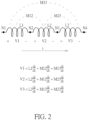
FIG. 2 is a diagram illustrating a tapped inductor within the oscillator according to one embodiment of the present invention. -
FIG. 3 is a diagram illustrating an oscillator according to one embodiment of the present invention. -
FIG. 4 is a diagram illustrating the tapped inductor according to a first embodiment of the present invention. -
FIG. 5 is a diagram illustrating the tapped inductor according to a second embodiment of the present invention. -
FIG. 6 is a diagram illustrating the tapped inductor according to a third embodiment of the present invention. - Certain terms are used throughout the following description and claims to refer to particular system components. As one skilled in the art will appreciate, manufacturers may refer to a component by different names. This document does not intend to distinguish between components that differ in name but not function. In the following discussion and in the claims, the terms "including" and "comprising" are used in an open-ended fashion, and thus should be interpreted to mean "including, but not limited to ...". The terms "couple" and "couples" are intended to mean either an indirect or a direct electrical connection. Thus, if a first device couples to a second device, that connection may be through a direct electrical connection, or through an indirect electrical connection via other devices and connections.
-
FIG. 1 is a diagram illustrating anoscillator 100 according to one embodiment of the present invention. As shown inFIG. 1 , theoscillator 100 comprises at least a cross-coupled pair including afirst device 110 and asecond device 120, acapacitor 130 and a tappedinductor 140. In this embodiment, two input signals Vinn and Vinp of the cross-coupled pair are coupled to two terminals N1 and N4 of the tappedinductor 140, and two output signals Voutn and Voutp of the cross-coupled pair are coupled to two taps N2 and N3 of the tappedinductor 140. Specifically, thefirst device 110 receives the input signal Vinp from the terminal N4 of the tappedinductor 140 to generate the output signal Voutn to the tap N2 of the tappedinductor 140, and thesecond device 120 receives the input signal Vinn from the terminal N1 of the tappedinductor 140 to generate the output signal Voutp to the tap N3 of the tappedinductor 140, wherein the two input signals Vinn and Vinp are differential signal, and the two out signals Voutn and Voutp are differential signal. In this embodiment, theoscillator 100 is a LC-tank digitally controlled oscillator (DCO) or voltage-controlled oscillator (VCO), and the two output signals Voutn and Voutp serve as oscillation signals of theoscillator 100. - In the embodiment shown in
FIG. 1 , the tappedinductor 140 of theoscillator 100 is a multi-turn tapped inductor, so the swing of the cross-coupled pair can be increased through its own mutual inductance, which in turn boosts the transconductance of the cross-coupled pair. Specifically, referring toFIG. 2 , the tappedinductor 140 comprises several inductors connected in series (in this embodiment, the tappedinductor 140 comprises three inductors), wherein the first inductor having inductance L1 is coupled between the terminal N1 and the tap N2, the second inductor having inductance L2 is coupled between taps N2 and N3, and the third inductor having inductance L3 is coupled between the tap N3 and the terminal N4. In this embodiment, there is a mutual inductance M12 between the first inductor and the second inductor, a mutual inductance M23 between the second inductor and the third inductor, and a mutual inductance M13 between the first inductor and the third inductor, so total inductance of the tappedinductor 140 is equal to "L1+L2+L3+2*M12+2*M13+2*M23", and a voltage difference V1 between the terminal N1 and the tap N2, a voltage difference V2 between the taps N2 and N3, and a voltage difference V3 between the tap N3 and the terminal N4 can be expressly as follows, wherein the symbol "i" is a current flowing through the tapped inductor 140:


- In the embodiment shown in
FIG. 1 , the cross-coupled pair is connected to have a positive feedback which generates negative resistance to sustain oscillation. In the conventional art that the output signals of the cross-coupled pair are connected to the terminals N1 and N4, the negative resistance is equal to "-2/gm", wherein the term "gm" is the transconductance of the cross-coupled pair. In the embodiment ofFIG. 1 , the negative resistance is equal to "-2/(gm*(1+2a))", wherein the term "α" is a ratio between "V1" and "V2". Therefore, sinceoscillator 100 of this embodiment has better negative resistance than the conventional art, the quality factor of theoscillator 100 becomes better. - In light of above, because the transconductance of the cross-coupled pair of the
oscillator 100 is increased at the same bias current, it can achieve the desired transconductance with low power consumption. In addition, because the quality factor of theoscillator 100 becomes better, the required quality factor can be achieved with a smaller chip area. Furthermore, the increased voltage swings at the terminals N1 and N4 result in lower phase noise. - In one embodiment, each of the
first device 110 and thesecond device 120 can be implemented by a transistor as shown inFIG. 3 . InFIG. 3 , thefirst device 110 is implemented by a transistor (N-type transistor) MN1, wherein the transistor MN1 receives the input signal Vinp at a gate electrode to generate the output signal Voutn at a drain electrode; and thesecond device 120 is implemented by a transistor (N-type transistor) MN2, wherein the transistor MN2 receives the input signal Vinn at a gate electrode to generate the output signal Voutp at a drain electrode. In addition, each of the taps N2 and N3 of the tappedinductor 140 may be connected to a supply voltage VDD viacomponents 310, wherein thecomponents 310 may comprise a current source couple between the supply voltage VDD and the drain electrodes of the transistors MN1 and MN2; or thecomponents 310 may comprise a P-type transistors couple between the supply voltage VDD and the drain electrodes of the transistors MN1 and MN2; or thecomponents 310 may comprise another cross-coupled pair couple between the supply voltage VDD and the drain electrodes of the transistors MN1 and MN2. Because the present invention focuses on the connections between thefirst device 110, thesecond device 120 and the tappedinductor 140, and a person skilled in the art should understand how to implement thecomponents 310, the details of thecomponents 310 and other portions of theoscillator 100 are not described here. - Regarding the tapped
inductor 140, in order to provide positive mutual inductance to boost the tanconductance of the cross-coupled pair, the tappedinductor 140 is designed to have multiple turns, and the inductors may share the same flux. TakingFIG. 2 as an example, the first inductor, the second inductor and the third inductor may have the same polarity, that is the terminal N1 may be a positive terminal for the first inductor, the tap N2 may be a positive terminal for the second inductor, and the tap N3 may be a positive terminal for the third inductor; or the terminal N1 may be a negative terminal for the first inductor, the tap N2 may be a negative terminal for the second inductor, and the tap N3 may be a negative terminal for the third inductor. -
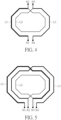
FIG. 4 is a diagram illustrating the tappedinductor 140 according to a first embodiment of the present invention. As shown inFIG. 4 , the tappedinductor 140 has two turns, wherein the left half of the outer turn of the tappedinductor 140 corresponds to the first inductor having the inductance L1 shown inFIG. 2 , the right half of the outer turn of the tappedinductor 140 corresponds to the third inductor having the inductance L3 shown inFIG. 2 , and the inner turn of the tappedinductor 140 corresponds to the second inductor having the inductance L2 shown inFIG. 2 . -
FIG. 5 is a diagram illustrating the tappedinductor 140 according to a second embodiment of the present invention. As shown inFIG. 5 , the tappedinductor 140 has three turns, wherein the left half of the outer turn and the right half of the middle turn of the tappedinductor 140 corresponds to the first inductor having the inductance L1 shown inFIG. 2 , the left half of the middle turn and the right half of the outer turn of the tappedinductor 140 corresponds to the third inductor having the inductance L3 shown inFIG. 2 , and the inner turn of the tappedinductor 140 corresponds to the second inductor having the inductance L2 shown inFIG. 2 . -
FIG. 6 is a diagram illustrating the tappedinductor 140 according to a third embodiment of the present invention. As shown inFIG. 6 , the tappedinductor 140 has three turns, wherein the left half of the middle turn and the right half of the outer turn of the tappedinductor 140 corresponds to the first inductor having the inductance L1 shown inFIG. 2 , the left half of the outer turn and the right half of the middle turn of the tappedinductor 140 corresponds to the third inductor having the inductance L3 shown inFIG. 2 , and the inner turn of the tappedinductor 140 corresponds to the second inductor having the inductance L2 shown inFIG. 2 . - Briefly summarized, in the oscillator of the present invention, by using the tapped inductor and connecting the output signals of the cross-coupled pair to the taps of the tapped inductor, the voltage swings at the terminals of the tapped inductor can be increased to lower the phase noise, and the transconductance of the cross-coupled pair can be increased accordingly.
- Those skilled in the art will readily observe that numerous modifications and alterations of the device and method may be made while retaining the teachings of the invention. Accordingly, the above disclosure should be construed as limited only by the metes and bounds of the appended claims.
Claims (10)
- An oscillator (100), comprising:a tapped inductor (140) comprising a first terminal (N1), a second terminal (N4), a first tap (N2) and a second tap (N3); anda cross-coupled pair, wherein the cross-coupled pair receives two input signals from the first terminal (N1) and the second terminal (N4) to generate two output signals to the first tap (N2) and the second tap (N3), respectively.
- The oscillator (100) of claim 1, wherein the two input signals comprise a first input signal (Vinn) and a second input signal (Vinp), the two output signals comprise a first output signal (Voutn) and a second output signal (Voutp), and the cross-coupled pair comprises a first device (110) and a second device (120); and the first device (110) receives the first input signal (Vinn) from the second terminal (N4) to generate the first output signal (Voutn) to the first tap (N2), and the second device (120) receives the second input signal (Vinp) from the first terminal (N1) to generate the second output signal (Voutp) to the second tap (N3) .
- The oscillator (100) of claim 2, wherein the first device (110) is implemented by a first transistor, a gate electrode of the first transistor is coupled to the second terminal (N4), and a drain electrode of the first transistor is coupled to the first tap (N2) ; and the second device (120) is implemented by a second transistor, a gate electrode of the second transistor is coupled to the first terminal (N1), and a drain electrode of the second transistor is coupled to the second tap (N3).
- The oscillator (100) of claim 1, further comprising:
a capacitor (130) coupled between the first tap (N2) and the second tap (N3). - The oscillator (100) of claim 1, wherein the tapped inductor (140) is a multi-turn tapped inductor (140).
- The oscillator (100) of claim 1, wherein the tapped inductor (140) comprises a first inductor, a second inductor and a third inductor connected in series, the first inductor is coupled between the first terminal (N1) and the first tap (N2), the second inductor is coupled between the first tap (N2) and the second tap (N3), and the third inductor is coupled between the second tap (N3) and the second terminal (N4).
- The oscillator (100) of claim 6, wherein the two input signals comprise a first input signal (Vinn) and a second input signal (Vinp), the two output signals comprise a first output signal (Voutn) and a second output signal (Voutp), and the cross-coupled pair comprises a first device (110) and a second device (120); and the first device (110) receives the first input signal (Vinn) from the second terminal (N4) to generate the first output signal (Voutn) to the first tap (N2), and the second device (120) receives the second input signal (Vinp) from the first terminal (N1) to generate the second output signal (Voutp) to the second tap (N3) .
- The oscillator (100) of claim 7, wherein the first device (110) is implemented by a first transistor, a gate electrode of the first transistor is coupled to the second terminal (N4), and a drain electrode of the first transistor is coupled to the first tap (N2) ; and the second device (120) is implemented by a second transistor, a gate electrode of the second transistor is coupled to the first terminal (N1), and a drain electrode of the second transistor is coupled to the second tap (N3).
- The oscillator (100) of claim 6, wherein the first inductor, the second inductor and the third inductor have the same polarity.
- The oscillator (100) of claim 6, wherein the first terminal (N1) is a positive terminal for the first inductor, the first tap (N2) is a positive terminal for the second inductor, and the second tap is a positive terminal for the third inductor; or the first terminal (N1) is a negative terminal for the first inductor, the first tap (N2) is a negative terminal for the second inductor, and the second tap (N3) is a negative terminal for the third inductor.
Applications Claiming Priority (2)
| Application Number | Priority Date | Filing Date | Title |
|---|---|---|---|
| US202163247814P | 2021-09-24 | 2021-09-24 | |
| CN202210566775.XA CN117155288A (en) | 2022-05-23 | 2022-05-23 | Oscillator |
Publications (1)
| Publication Number | Publication Date |
|---|---|
| EP4156505A1 true EP4156505A1 (en) | 2023-03-29 |
Family
ID=82321464
Family Applications (1)
| Application Number | Title | Priority Date | Filing Date |
|---|---|---|---|
| EP22181127.6A Withdrawn EP4156505A1 (en) | 2021-09-24 | 2022-06-25 | Oscillator with tapped inductor |
Country Status (3)
| Country | Link |
|---|---|
| US (1) | US11770100B2 (en) |
| EP (1) | EP4156505A1 (en) |
| TW (1) | TWI806682B (en) |
Citations (3)
| Publication number | Priority date | Publication date | Assignee | Title |
|---|---|---|---|---|
| EP3157167A1 (en) * | 2015-10-14 | 2017-04-19 | MediaTek Inc. | Lc-tank oscillator having intrinsic low-pass filter |
| US20190372523A1 (en) * | 2015-03-16 | 2019-12-05 | Futurewei Technologies, Inc. | Tapped inductor voltage controlled oscillator |
| WO2021081955A1 (en) * | 2019-10-31 | 2021-05-06 | 华为技术有限公司 | Oscillator circuit |
Family Cites Families (1)
| Publication number | Priority date | Publication date | Assignee | Title |
|---|---|---|---|---|
| US7583156B2 (en) * | 2007-05-10 | 2009-09-01 | Texas Instruments Incorporated | Oscillator with multi-tap inductor, capacitors, and negative-Gm stages |
-
2022
- 2022-06-24 US US17/848,415 patent/US11770100B2/en active Active
- 2022-06-25 EP EP22181127.6A patent/EP4156505A1/en not_active Withdrawn
- 2022-06-30 TW TW111124493A patent/TWI806682B/en active
Patent Citations (3)
| Publication number | Priority date | Publication date | Assignee | Title |
|---|---|---|---|---|
| US20190372523A1 (en) * | 2015-03-16 | 2019-12-05 | Futurewei Technologies, Inc. | Tapped inductor voltage controlled oscillator |
| EP3157167A1 (en) * | 2015-10-14 | 2017-04-19 | MediaTek Inc. | Lc-tank oscillator having intrinsic low-pass filter |
| WO2021081955A1 (en) * | 2019-10-31 | 2021-05-06 | 华为技术有限公司 | Oscillator circuit |
Also Published As
| Publication number | Publication date |
|---|---|
| TW202315302A (en) | 2023-04-01 |
| TWI806682B (en) | 2023-06-21 |
| US20230100708A1 (en) | 2023-03-30 |
| US11770100B2 (en) | 2023-09-26 |
Similar Documents
| Publication | Publication Date | Title |
|---|---|---|
| US20070241826A1 (en) | Oscillating circuit | |
| US9214929B2 (en) | Waveform conversion circuit with reduced jitter | |
| US20110291724A1 (en) | Duty cycle correction circuit | |
| US7408422B2 (en) | Variable-capacitance circuit element | |
| US20090033430A1 (en) | Injection-locked frequency divider | |
| EP3157167B1 (en) | Lc-tank oscillator having intrinsic low-pass filter | |
| US20070182616A1 (en) | Capacitor-coupled level shifter with duty-cycle independence and supply referenced bias configuration | |
| KR101209405B1 (en) | low phase noise amplifier circuit | |
| CN101557213A (en) | Delay unit, annular oscillator and PLL circuit | |
| WO2008002792A2 (en) | Versatile and compact dc-coupled cml buffer | |
| US20060181356A1 (en) | Quadrature voltage controlled oscillator | |
| US20050046494A1 (en) | Low power quadrature voltage controlled oscillator using back gate | |
| CN107070405A (en) | Oscillator device | |
| US8432222B2 (en) | Apparatus and methods for electronic amplification | |
| US9964985B1 (en) | Radio frequency power amplifier and method thereof | |
| EP3200343B1 (en) | Power amplifier system and associated bias circuit | |
| US11770100B2 (en) | Oscillator with tapped inductor | |
| US8274320B2 (en) | Signal processing circuit with improved linearity | |
| KR100431999B1 (en) | A Self-Regulating Voltage Controlled Oscillator | |
| US7295072B2 (en) | Amplifier circuit | |
| CN110708046B (en) | A device and method for generating a quadrature local oscillator signal with a duty cycle of 25% | |
| EP3355471A1 (en) | Class ab amplifier having cascode stage with filter for improving linearity | |
| CN210724717U (en) | Orthogonal local oscillator signal generating device with duty ratio of 25% | |
| US10951185B2 (en) | Differential amplifier circuit and serial transmission circuit | |
| CN117155288A (en) | Oscillator |
Legal Events
| Date | Code | Title | Description |
|---|---|---|---|
| PUAI | Public reference made under article 153(3) epc to a published international application that has entered the european phase |
Free format text: ORIGINAL CODE: 0009012 |
|
| STAA | Information on the status of an ep patent application or granted ep patent |
Free format text: STATUS: THE APPLICATION HAS BEEN PUBLISHED |
|
| AK | Designated contracting states |
Kind code of ref document: A1 Designated state(s): AL AT BE BG CH CY CZ DE DK EE ES FI FR GB GR HR HU IE IS IT LI LT LU LV MC MK MT NL NO PL PT RO RS SE SI SK SM TR |
|
| P01 | Opt-out of the competence of the unified patent court (upc) registered |
Effective date: 20230607 |
|
| STAA | Information on the status of an ep patent application or granted ep patent |
Free format text: STATUS: THE APPLICATION IS DEEMED TO BE WITHDRAWN |
|
| 18D | Application deemed to be withdrawn |
Effective date: 20230930 |