EP4156478A1 - Power inverter device with optimized switching behavior - Google Patents
Power inverter device with optimized switching behavior Download PDFInfo
- Publication number
- EP4156478A1 EP4156478A1 EP21198327.5A EP21198327A EP4156478A1 EP 4156478 A1 EP4156478 A1 EP 4156478A1 EP 21198327 A EP21198327 A EP 21198327A EP 4156478 A1 EP4156478 A1 EP 4156478A1
- Authority
- EP
- European Patent Office
- Prior art keywords
- switching
- control unit
- dead time
- voltage
- unit
- Prior art date
- Legal status (The legal status is an assumption and is not a legal conclusion. Google has not performed a legal analysis and makes no representation as to the accuracy of the status listed.)
- Withdrawn
Links
- 230000002596 correlated effect Effects 0.000 claims abstract description 7
- 238000000034 method Methods 0.000 claims description 20
- 238000012360 testing method Methods 0.000 claims description 15
- 239000004065 semiconductor Substances 0.000 claims description 8
- 230000005669 field effect Effects 0.000 claims description 7
- 230000000875 corresponding effect Effects 0.000 claims description 6
- 238000012804 iterative process Methods 0.000 claims description 6
- 238000004364 calculation method Methods 0.000 claims description 4
- 230000008569 process Effects 0.000 description 6
- 230000006399 behavior Effects 0.000 description 5
- 239000003990 capacitor Substances 0.000 description 3
- 230000006870 function Effects 0.000 description 3
- 238000004422 calculation algorithm Methods 0.000 description 2
- 230000008859 change Effects 0.000 description 2
- 230000001976 improved effect Effects 0.000 description 2
- 230000001939 inductive effect Effects 0.000 description 2
- 229910044991 metal oxide Inorganic materials 0.000 description 2
- 150000004706 metal oxides Chemical class 0.000 description 2
- 238000011084 recovery Methods 0.000 description 2
- 230000009471 action Effects 0.000 description 1
- 230000000295 complement effect Effects 0.000 description 1
- 230000001276 controlling effect Effects 0.000 description 1
- 238000013461 design Methods 0.000 description 1
- 238000011065 in-situ storage Methods 0.000 description 1
- 230000000977 initiatory effect Effects 0.000 description 1
- 238000012423 maintenance Methods 0.000 description 1
- 238000007620 mathematical function Methods 0.000 description 1
- 230000003071 parasitic effect Effects 0.000 description 1
- 238000012545 processing Methods 0.000 description 1
- 238000010998 test method Methods 0.000 description 1
- 230000001960 triggered effect Effects 0.000 description 1
Images
Classifications
-
- H—ELECTRICITY
- H02—GENERATION; CONVERSION OR DISTRIBUTION OF ELECTRIC POWER
- H02M—APPARATUS FOR CONVERSION BETWEEN AC AND AC, BETWEEN AC AND DC, OR BETWEEN DC AND DC, AND FOR USE WITH MAINS OR SIMILAR POWER SUPPLY SYSTEMS; CONVERSION OF DC OR AC INPUT POWER INTO SURGE OUTPUT POWER; CONTROL OR REGULATION THEREOF
- H02M1/00—Details of apparatus for conversion
- H02M1/0048—Circuits or arrangements for reducing losses
- H02M1/0054—Transistor switching losses
-
- H—ELECTRICITY
- H02—GENERATION; CONVERSION OR DISTRIBUTION OF ELECTRIC POWER
- H02M—APPARATUS FOR CONVERSION BETWEEN AC AND AC, BETWEEN AC AND DC, OR BETWEEN DC AND DC, AND FOR USE WITH MAINS OR SIMILAR POWER SUPPLY SYSTEMS; CONVERSION OF DC OR AC INPUT POWER INTO SURGE OUTPUT POWER; CONTROL OR REGULATION THEREOF
- H02M1/00—Details of apparatus for conversion
- H02M1/0003—Details of control, feedback or regulation circuits
- H02M1/0012—Control circuits using digital or numerical techniques
-
- H—ELECTRICITY
- H02—GENERATION; CONVERSION OR DISTRIBUTION OF ELECTRIC POWER
- H02M—APPARATUS FOR CONVERSION BETWEEN AC AND AC, BETWEEN AC AND DC, OR BETWEEN DC AND DC, AND FOR USE WITH MAINS OR SIMILAR POWER SUPPLY SYSTEMS; CONVERSION OF DC OR AC INPUT POWER INTO SURGE OUTPUT POWER; CONTROL OR REGULATION THEREOF
- H02M1/00—Details of apparatus for conversion
- H02M1/08—Circuits specially adapted for the generation of control voltages for semiconductor devices incorporated in static converters
-
- H—ELECTRICITY
- H02—GENERATION; CONVERSION OR DISTRIBUTION OF ELECTRIC POWER
- H02M—APPARATUS FOR CONVERSION BETWEEN AC AND AC, BETWEEN AC AND DC, OR BETWEEN DC AND DC, AND FOR USE WITH MAINS OR SIMILAR POWER SUPPLY SYSTEMS; CONVERSION OF DC OR AC INPUT POWER INTO SURGE OUTPUT POWER; CONTROL OR REGULATION THEREOF
- H02M1/00—Details of apparatus for conversion
- H02M1/38—Means for preventing simultaneous conduction of switches
-
- H—ELECTRICITY
- H02—GENERATION; CONVERSION OR DISTRIBUTION OF ELECTRIC POWER
- H02M—APPARATUS FOR CONVERSION BETWEEN AC AND AC, BETWEEN AC AND DC, OR BETWEEN DC AND DC, AND FOR USE WITH MAINS OR SIMILAR POWER SUPPLY SYSTEMS; CONVERSION OF DC OR AC INPUT POWER INTO SURGE OUTPUT POWER; CONTROL OR REGULATION THEREOF
- H02M1/00—Details of apparatus for conversion
- H02M1/38—Means for preventing simultaneous conduction of switches
- H02M1/385—Means for preventing simultaneous conduction of switches with means for correcting output voltage deviations introduced by the dead time
-
- H—ELECTRICITY
- H02—GENERATION; CONVERSION OR DISTRIBUTION OF ELECTRIC POWER
- H02M—APPARATUS FOR CONVERSION BETWEEN AC AND AC, BETWEEN AC AND DC, OR BETWEEN DC AND DC, AND FOR USE WITH MAINS OR SIMILAR POWER SUPPLY SYSTEMS; CONVERSION OF DC OR AC INPUT POWER INTO SURGE OUTPUT POWER; CONTROL OR REGULATION THEREOF
- H02M7/00—Conversion of AC power input into DC power output; Conversion of DC power input into AC power output
- H02M7/42—Conversion of DC power input into AC power output without possibility of reversal
- H02M7/44—Conversion of DC power input into AC power output without possibility of reversal by static converters
- H02M7/48—Conversion of DC power input into AC power output without possibility of reversal by static converters using discharge tubes with control electrode or semiconductor devices with control electrode
- H02M7/53—Conversion of DC power input into AC power output without possibility of reversal by static converters using discharge tubes with control electrode or semiconductor devices with control electrode using devices of a triode or transistor type requiring continuous application of a control signal
- H02M7/537—Conversion of DC power input into AC power output without possibility of reversal by static converters using discharge tubes with control electrode or semiconductor devices with control electrode using devices of a triode or transistor type requiring continuous application of a control signal using semiconductor devices only, e.g. single switched pulse inverters
- H02M7/5387—Conversion of DC power input into AC power output without possibility of reversal by static converters using discharge tubes with control electrode or semiconductor devices with control electrode using devices of a triode or transistor type requiring continuous application of a control signal using semiconductor devices only, e.g. single switched pulse inverters in a bridge configuration
-
- H—ELECTRICITY
- H02—GENERATION; CONVERSION OR DISTRIBUTION OF ELECTRIC POWER
- H02M—APPARATUS FOR CONVERSION BETWEEN AC AND AC, BETWEEN AC AND DC, OR BETWEEN DC AND DC, AND FOR USE WITH MAINS OR SIMILAR POWER SUPPLY SYSTEMS; CONVERSION OF DC OR AC INPUT POWER INTO SURGE OUTPUT POWER; CONTROL OR REGULATION THEREOF
- H02M7/00—Conversion of AC power input into DC power output; Conversion of DC power input into AC power output
- H02M7/42—Conversion of DC power input into AC power output without possibility of reversal
- H02M7/44—Conversion of DC power input into AC power output without possibility of reversal by static converters
- H02M7/48—Conversion of DC power input into AC power output without possibility of reversal by static converters using discharge tubes with control electrode or semiconductor devices with control electrode
- H02M7/53—Conversion of DC power input into AC power output without possibility of reversal by static converters using discharge tubes with control electrode or semiconductor devices with control electrode using devices of a triode or transistor type requiring continuous application of a control signal
- H02M7/537—Conversion of DC power input into AC power output without possibility of reversal by static converters using discharge tubes with control electrode or semiconductor devices with control electrode using devices of a triode or transistor type requiring continuous application of a control signal using semiconductor devices only, e.g. single switched pulse inverters
- H02M7/5387—Conversion of DC power input into AC power output without possibility of reversal by static converters using discharge tubes with control electrode or semiconductor devices with control electrode using devices of a triode or transistor type requiring continuous application of a control signal using semiconductor devices only, e.g. single switched pulse inverters in a bridge configuration
- H02M7/53871—Conversion of DC power input into AC power output without possibility of reversal by static converters using discharge tubes with control electrode or semiconductor devices with control electrode using devices of a triode or transistor type requiring continuous application of a control signal using semiconductor devices only, e.g. single switched pulse inverters in a bridge configuration with automatic control of output voltage or current
-
- H—ELECTRICITY
- H02—GENERATION; CONVERSION OR DISTRIBUTION OF ELECTRIC POWER
- H02M—APPARATUS FOR CONVERSION BETWEEN AC AND AC, BETWEEN AC AND DC, OR BETWEEN DC AND DC, AND FOR USE WITH MAINS OR SIMILAR POWER SUPPLY SYSTEMS; CONVERSION OF DC OR AC INPUT POWER INTO SURGE OUTPUT POWER; CONTROL OR REGULATION THEREOF
- H02M7/00—Conversion of AC power input into DC power output; Conversion of DC power input into AC power output
- H02M7/42—Conversion of DC power input into AC power output without possibility of reversal
- H02M7/44—Conversion of DC power input into AC power output without possibility of reversal by static converters
- H02M7/48—Conversion of DC power input into AC power output without possibility of reversal by static converters using discharge tubes with control electrode or semiconductor devices with control electrode
- H02M7/53—Conversion of DC power input into AC power output without possibility of reversal by static converters using discharge tubes with control electrode or semiconductor devices with control electrode using devices of a triode or transistor type requiring continuous application of a control signal
- H02M7/537—Conversion of DC power input into AC power output without possibility of reversal by static converters using discharge tubes with control electrode or semiconductor devices with control electrode using devices of a triode or transistor type requiring continuous application of a control signal using semiconductor devices only, e.g. single switched pulse inverters
- H02M7/5387—Conversion of DC power input into AC power output without possibility of reversal by static converters using discharge tubes with control electrode or semiconductor devices with control electrode using devices of a triode or transistor type requiring continuous application of a control signal using semiconductor devices only, e.g. single switched pulse inverters in a bridge configuration
- H02M7/53871—Conversion of DC power input into AC power output without possibility of reversal by static converters using discharge tubes with control electrode or semiconductor devices with control electrode using devices of a triode or transistor type requiring continuous application of a control signal using semiconductor devices only, e.g. single switched pulse inverters in a bridge configuration with automatic control of output voltage or current
- H02M7/53873—Conversion of DC power input into AC power output without possibility of reversal by static converters using discharge tubes with control electrode or semiconductor devices with control electrode using devices of a triode or transistor type requiring continuous application of a control signal using semiconductor devices only, e.g. single switched pulse inverters in a bridge configuration with automatic control of output voltage or current with digital control
Definitions
- the invention relates to a power inverter device and a vehicle comprising such a power inverter device .
- Modern power electronic inverters usually comprise at least one half bridge having one high side and one low side switch that are connected in series, or a combination of multiple half bridges.
- the dead time defines a time span between switch-off of one and switch-on of the complementary switch or vice-versa. For ideal switches this time may be 0s.
- semiconductors are not ideal due to rise and fall times as well as parasitic components, a value in the range of some nanoseconds with wide band gap semiconductors up to some milliseconds with thyristors need to be chosen.
- the dead time influences the resulting switching behavior and switching losses. These losses may increase up to more than 20% only by choosing the wrong parameters for dead time.
- the values for rise and fall time and therefore the optimal dead time depend on the actual load current and voltage level.
- a power inverter device comprising at least one half bridge having a DC voltage input, a first switching unit and a second switching unit for supplying an electric consumer with a modulated voltage on a voltage output, a gate driver, a control unit, and at least one sensor, wherein the at least one half bridge is connected to the voltage input, wherein the at least one half bridge is designed to selectively switch the first switching unit and the second switching unit into a closed state or an open state, wherein the gate driver is in a signal connection with the at least one half bridge and is adapted to generate at least one switching signal transferrable to the at least one half bridge to alternatingly switch the respective switching units with a switching pattern having a dead time between consecutive switching sequences, wherein the at least one sensor is adapted for measuring an electric parameter in the form of at least one of a voltage and a current at the voltage output, wherein the control unit is in signal connection with the gate driver and is adapted to control the gate driver to at least influence the dead time, and wherein the control unit is in signal connection
- the power inverter device comprises an electric circuit that is adapted for providing an alternating current (AC) for an electric machine from a DC source.
- the at least one half bridge is used, which may be designed according to commonly known half bridges.
- a half bridge may be associated to the gate driver and comprises the pair of the first and second switching units, which may exemplarily be realized in the form of field effect transistors (FETs).
- FETs field effect transistors
- the first switching unit may be considered a "high side” switching unit, while the second switching unit may be considered a "low side” switching unit.
- the gate driver is provided for initiating the switching action of the first and second switches to selectively couple the DC voltage source or a reference voltage, such as the ground voltage, to the voltage output. By using a certain switching pattern, the characteristics of the generated modulated, i.e. alternating, current is influenced.
- the gate driver is in a signal connection with the at least one half bridge and continuously sends the at least one switching signal to the switches.
- the at least one switching signal may be based on a PWM signal or similar. In the context of the invention it is required to avoid a short circuit by putting both the first and second switch into the closed state at the same time through using the above-identified dead time between two consecutive switching signals to put both switching units into the closed state.
- the at least one sensor is arranged to measure the voltage or the current at the voltage output. It may be a part of the control unit or be provided as a separate unit.
- the at least one sensor allows a feedback of momentary electric parameters to the control unit to allow the control unit to suitably adjust the switching pattern in-situ. While it is advantageous to measure the current and the voltage, it may also be possible to measure just one of the current and the voltage.
- control unit Through the signal connection between the control unit and the gate driver, the control unit is able to control the behavior of the gate driver. It is conceivable that the control unit is able to send control signals to the gate driver that at least leads to an adjustment of the dead time in the at least one switching signal. However, it may also be conceivable that the control unit further adjusts the switching pattern in general, in order to increase or decrease a switching frequency or other parameters.
- the control unit may comprise a signal input, which receives a frequency or rotational speed demand from another entity, which is processed to control the gate driver in a suitable way.
- a gist of the invention lies in providing a simplified and very effective way to control the at least one half bridge for improving the efficiency of the inverter device.
- the at least one half bridge needs to be analyzed in order to evaluate the voltage- and current-depending switching behavior. This may exemplarily be accomplished by a double pulse test. It is conceivable that the power inverter device is coupled with a DC power supply and an inductive load. The gate driver will be triggered to initiate switching the switching units into the closed or open state. A number of switching cycles may be done, wherein switching losses are measured preferably at each cycle.
- a change in switching losses can be recognized and ideal operating points can be identified, where the switching losses are minimum. For example, if the dead time is too small, losses in the power inverter device increase according to a certain shoot-through. This means, that a high side and a low side switch are conducting at the same time for a short instance. If the value for the dead time is too high, an antiparallel diode, such as a MOSFET or SiC diode, may start conducting for a short instance, which resultantly leads to additional losses. In particular, a reverse recovery charge that is stored in such a diode leads to an increase of switching losses.
- an antiparallel diode such as a MOSFET or SiC diode
- the minimum switching losses may usually arise in the point, where the diode is completely shunted by the parallel switching unit and therefore does not conduct, while the dead time is sufficiently large to avoid a short circuit. Then, the circuit shows almost no reverse recovery and therefore a much smoother switching behavior with less disturbances and overshoot is achieved. Additionally the influence of the snappy diode can be minimized.
- these may be stored in the control unit, together with associated current and/or voltage values. This allows the control unit to retrieve predetermined optimum dead time values for a momentary operating point that is measured by the at least one sensor. Thus, the control unit does not need to conduct a closed loop control of the switching units, but it may simply apply previously identified optimum parameters, such as optimum dead time values.
- the identification of these optimum parameters may be conducted through an external, separate initialization unit, which is connectable to the at least one half bridge. The identified parameters may then be transferred to the control unit to be used during normal operation of the power inverter device.
- the initialization unit may be used just once, i.e. a single time, before the power inverter device is used.
- control unit itself may be able to conduct such a process for identification if optimum parameters. It is furthermore conceivable that the process for identification, either conducted by an initialization unit or the control unit, may be conducted in a predetermined time interval, e.g. during a maintenance operation.
- the data set comprises a three-dimensional data set of dead time, current and voltage values
- the control unit is adapted for interpolating a desired dead time value depending on the measured electric parameters.
- the control unit may be adapted for a trilinear or tricubic interpolation, in order to identify an optimum dead time value for a given voltage and current value.
- the interpolation is based on an as simple algorithm as possible, which may include the trilinear interpolation.
- control unit may also be adapted for identification of a nearest dead time value for given voltage and current values, which may further reduce the effort in retrieving a suitable dead time value.
- the data set comprises a look-up table. It may be understood as an array of parameters, which may include values for the dead time, the current and the voltage, which are associated with each other.
- the control unit may load the look-up table at the start of operation into a memory unit. During the operation, the control unit may simply select dead time values that are associated with measured current and voltage values. It may be advantageous if the control unit conducts an interpolation or selects the dead time values that are nearest to the measured current and voltage values.
- the control unit may be adapted for creating at least a part of the data set through calculation from a predefined analytic formula. It is conceivable that the dead time may follow a certain mathematical relationship to the current and voltage values. The relationship may be identified through conducting the double pulse test or a similar process, as explained above. Instead of storing an array of different values it may be possible to define an approximation through a mathematical function. Such a function may e.g. be of a first, second, third or fourth order. The control unit may thus simply approximate a value for a required dead time from measured current and voltage values through such a formula.
- the formula may e.g. include a polynomial function.
- control unit or an external initialization unit which is couplable with the control unit, is adapted to measure switching parameters of the at least one half bridge through conducting double-pulse tests at different voltages and/or currents, wherein the control unit or the external initialization unit is adapted to vary the dead time through a range of different dead times in an iterative process when conducting the double-pulse tests, such that the control unit or the external initialization unit is able to monitor resulting switching losses at the different voltages and/or currents, and wherein the control unit is adapted to store dead time values corresponding to minimum switching losses for the different voltages and/or currents.
- a double-pule test is a feasible method for measuring switching parameters of semiconductor switching units, which allows to analyze and thus optimize the behavior of the power inverter device.
- Either the control unit itself or a separate component in the form of an initialization unit may be used for this process. If an external initialization unit is used, the control unit may comprise a simpler design and requires less functions and processing power. As explained above, it is conceivable that the process of identification of the optimum dead time values is conducted only once, as the results from the process provide the basis for a continuous, optimized operation.
- At least one of the first switching unit and the second switching unit may comprise at least one semiconductor switch, in particular a field-effect transistor switch or insulated gate bipolar transistors.
- semiconductor switch in particular a field-effect transistor switch or insulated gate bipolar transistors.
- These may include n-MOSFETs (n-type metal oxide semiconductor field-effect transistors, enhancement type), JFETs (junction field-effect transistors) or p-MOSFETs (p-type metal oxide semiconductor field-effect transistors).
- the switching units may also have IGBTs (Insulated Gate Bipolar Transistors).
- the power inverter device may comprise n half-bridges, each having a first switching unit and a second switching unit, for supplying an n-phase electrical machine with an n-phase supply voltage via phase connections assigned to the respective half-bridges, where n is at least 2. All half bridges may be analyzed to identify the respective optimum dead time values.
- the control unit as well as the gate driver are adapted to control all of the half-bridges to provide a modulated, alternating voltage for an electric consumer in the form of an electric machine that requires n phases. For example, the number of phases may be three.
- the invention further relates to a vehicle comprising a DC voltage source, an AC voltage electric machine, and at least one power inverter device according to the above description, wherein the electric machine is couplable to the voltage output of the at least one power inverter device, and wherein the at least one power inverter device is couplable with the DC voltage source.
- the electric machine may be a drive unit for providing thrust or a movement of a mechanical element that is installed in the vehicle, such as a lift influencing surface or a landing gear of an aircraft.
- the vehicle may be an aircraft.
- the aircraft may be a commercial or a military aircraft.
- the invention further relates to a method for operating a power inverter device, comprising generating at least one switching signal by a gate driver, which is in a signal connection with at least one half bridge having a DC voltage input, a first switching unit and a second switching unit for supplying an electric consumer with a modulated voltage on a voltage output, for alternatingly switching the respective switching units into a closed or open state with a switching pattern having a dead time between consecutive switching sequences, measuring an electric parameter in the form of at least one of a voltage and a current at the voltage output through at least one sensor, and adjusting the dead time depending on the measured electric parameter and a data set of measured electric parameters and correlated, predetermined dead time values through a control unit, which is in signal connection with the at least one sensor.
- the method may further comprise measuring switching parameters of the at least one half bridge by the control unit or an external initialization unit, which is couplable with the control unit, through conducting double-pulse tests at different voltages and/or currents, varying the dead time through a range of different dead times in an iterative process when conducting the double-pulse tests through the control unit or the external initialization unit, such that the control unit or the external initialization unit is able to monitor resulting switching losses at the different voltages and/or currents, and storing dead time values corresponding to minimum switching losses for the different voltages and/or currents by the control unit.
- the data set may comprise a three-dimensional data set of dead time, current and voltage values, wherein the method may further comprise interpolating a desired dead time value depending on the measured electric parameters by the control unit.
- the method may further comprise creating at least a part of the data set through calculation from a predefined analytic formula by the control unit.
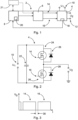
- Fig. 1 shows a power inverter device 2 comprising a half bridge 4, which is coupled with a gate driver 6, which in turn is coupled with a control unit 8.
- the half bridge 4 is connected to a DC voltage input 10, which delivers a DC voltage U 1 .
- the half bridge 4 is used for providing a modulated voltage U 2 at a voltage output 12.
- the gate driver 6 is in a signal connection with the half bridge 4 and is adapted to generate switching signals transferable to the half bridge 4, in order to change the switching state of two switching units (not shown in this illustration) inside the half bridge 4.
- the gate driver 6 delivers a first signal 14 to switch a high side of the half bridge 4 as well as a second signal 16 to switch a low side of the half bridge 4. In doing so, the modulated, i.e. alternating, voltage U 2 is created.
- the control unit eight is adapted to control the gate driver 6 to at least influence the dead time between consecutive switching sequences initiated by the first signal 14 and the second signal 16.
- the control unit 8 in turn is adapted to adjust the dead time depending on the measured electric parameters and a data set, in which several values for the voltage and/or current are correlated with predetermined optimum dead time values.
- the control unit 8 may comprise a memory unit 20, which is able store and provide such a data set. The control unit 8 may load the data set from the memory unit 20 and select suitable dead time values depending on momentary current and/or voltage values.
- control unit 8 or another entity such as an external initialization unit 21, which is shown as an alternative with dashed lines, may be adapted to measure switching parameters of the half bridge 4.
- the control unit 8 or the initialization unit 21, respectively is adapted to measure switching parameters of the half bridge 4 through conducting double-pulse tests at different voltages and/or currents.
- the control unit 8 or the external initialization unit 21 is adapted to vary the dead time through a range of different dead times in an iterative process when conducting the double-pulse tests, such that the control unit 8, or the external initialization unit 21, is able to monitor resulting switching losses at the different voltages and/or currents.
- control unit 8 stores dead time values corresponding to minimum switching losses for the different voltages and/or currents in the memory unit 20. This may either be done after receiving the respective values from the initialization unit 21 or directly from an algorithm running in the control unit 8, depending on the desired setup.
- Fig. 2 shows the half bridge 4 in further detail.
- the half bridge 4 is supplied with the DC voltage U 1 at the voltage input 10. Furthermore, an intermediate capacitor 22 is provided.
- One terminal of the voltage input 10 is connected to a high potential, while the other terminal is at a low potential, for example ground.
- the top terminal relates to the high potential and the bottom terminal to the low potential.
- the half bridge 4 comprises a first switching unit 24 and a second switching unit 26, which both are realized in the form of a semiconductor switch, such as field-effect transistor switches, e.g. n-MOSFETs, JFETs or p-MOSFETs. However, they may also comprise IGBTs.
- the switching units 24 and 26 generate a modulated, i.e. alternating, voltage at the voltage output 12 for supplying an electric consumer.
- the switching units 24 and 26 are controlled by the gate driver 6 to alternately switch the phase terminal of the voltage output 12 against the voltage U 1 or ground. For this, the switching units 24 and 26 receive the first signal 14 and the second signal, respectively.
- both switching units 24 and 26 comprise an antiparallel diode 28, e.g. a body diode, that allows to provide a reverse current path, e.g. for instances where both switching units 24 and 26 are turned off.
- an antiparallel diode 28 e.g. a body diode
- Fig. 3 shows the signals 14 and 16 provided by the gate driver 6 and received by the switching units 24 and 26 over time.
- the signals 14 and 16 are generated alternately, such that the switching units 24 and 26 switch alternately.
- a dead time 30 is included, the length of which is influenced by the control unit 8 as stated above.
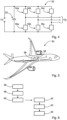
- Fig. 4 exemplarily shows a modified half bridge arrangement 32 based on three half bridges 4 sharing a single intermediate capacitor 22 and having three sets of switching units 24a, 26a, 24b, 26b, 24c, 26c, which are used for generating a three-phase output voltage U 2 .
- a respective gate driver would be adapted for generating signals 14a, 16a, 14b, 16b, 14c and 16c to initiate the switching of the switching units 24a, 26a, 24b, 26b, 24c, 26c.
- the basic principle of providing a dead time between consecutive switching signals corresponds to the above.
- Fig. 5 shows an aircraft 34, which comprises at least one electric consumer 36, such as an electric machine, which is indicated by a box having dashed lines. It may be any kind of electric consumer and in particular any inductive load.
- the electric consumer 36 is connected to a power inverter device 2, which in turn is connected to a voltage source, in particular a high DC voltage source 38.
- Fig. 6 shows a method for operating the power inverter device 2 in a block-oriented, schematic view.
- the method comprises generating 40 at least one switching signal 14, 16 by the gate driver 6, which is in a signal connection with the half bridge 4 having the DC voltage input 10, the first switching unit 24 and the second switching unit 26 for supplying the electric consumer 36 with a modulated voltage on the voltage output 12, for alternatingly switching the respective switching units 24, 26 into a closed or open state with a switching pattern having the dead time 30 between consecutive switching sequences.
- An electric parameter in the form of at least one of a voltage and a current at the voltage output 12 through the sensor 18 is measured 42.
- the dead time 30 is adjusted 44 depending on the measured electric parameter and a data set of measured electric parameters and correlated, predetermined dead time values through the control unit 8, which is in signal connection with the sensor 18.
- the method Prior to operating the power inverter device 2, the method comprises measuring 46 switching parameters of the at least one half bridge 4 by the control unit 8 or the external initialization unit 21, which is couplable with the control unit 8, through conducting double-pulse tests at different voltages and/or currents.
- the dead time 30 is varied 48 through a range of different dead times 30 in an iterative process when conducting the double-pulse tests through the control unit 8 or the external initialization unit 21, such that the control unit 8 or the external initialization unit 21 is able to monitor resulting switching losses at the different voltages and/or currents.
- dead time values corresponding to minimum switching losses for the different voltages and/or currents are stored 50 by the control unit 8.
Landscapes
- Engineering & Computer Science (AREA)
- Power Engineering (AREA)
- Inverter Devices (AREA)
Abstract
A power inverter device is proposed, comprising at least one half bridge having a DC voltage input, a first switching unit and a second switching unit for supplying an electric consumer with a modulated voltage on a voltage output, a gate driver, a control unit, and at least one sensor, wherein the at least one half bridge is connected to the voltage input, wherein the at least one half bridge is designed to selectively switch the first switching unit and the second switching unit into a closed state or an open state, wherein the gate driver is in a signal connection with the at least one half bridge and is adapted to generate at least one switching signal transferrable to the at least one half bridge to alternatingly switch the respective switching units with a switching pattern having a dead time between consecutive switching sequences, wherein the at least one sensor is adapted for measuring an electric parameter in the form of at least one of a voltage and a current at the voltage output, wherein the control unit is in signal connection with the gate driver and is adapted to control the gate driver to at least influence the dead time, and wherein the control unit is in signal connection with the at least one sensor and is further adapted to adjust the dead time depending on the measured electric parameter and a data set of measured electric parameters and correlated, predetermined dead time values.
Description
- The invention relates to a power inverter device and a vehicle comprising such a power inverter device .
- Modern power electronic inverters usually comprise at least one half bridge having one high side and one low side switch that are connected in series, or a combination of multiple half bridges. To avoid a short circuit caused by a switched-on high side and low side switch at the same time, an inserted so called dead time is necessary. The dead time defines a time span between switch-off of one and switch-on of the complementary switch or vice-versa. For ideal switches this time may be 0s. As semiconductors are not ideal due to rise and fall times as well as parasitic components, a value in the range of some nanoseconds with wide band gap semiconductors up to some milliseconds with thyristors need to be chosen. However, the dead time influences the resulting switching behavior and switching losses. These losses may increase up to more than 20% only by choosing the wrong parameters for dead time. In addition, the values for rise and fall time and therefore the optimal dead time depend on the actual load current and voltage level.
- It is an object of the invention to propose an improved power inverter circuit, which has a significantly reduced switching loss and an improved overall efficiency.
- The object is met by a power inverter circuit having the features of independent claim 1. Advantageous embodiments and further improvements may be gathered from the subclaims and the following description.
- A power inverter device is proposed, comprising at least one half bridge having a DC voltage input, a first switching unit and a second switching unit for supplying an electric consumer with a modulated voltage on a voltage output, a gate driver, a control unit, and at least one sensor, wherein the at least one half bridge is connected to the voltage input, wherein the at least one half bridge is designed to selectively switch the first switching unit and the second switching unit into a closed state or an open state, wherein the gate driver is in a signal connection with the at least one half bridge and is adapted to generate at least one switching signal transferrable to the at least one half bridge to alternatingly switch the respective switching units with a switching pattern having a dead time between consecutive switching sequences, wherein the at least one sensor is adapted for measuring an electric parameter in the form of at least one of a voltage and a current at the voltage output, wherein the control unit is in signal connection with the gate driver and is adapted to control the gate driver to at least influence the dead time, and wherein the control unit is in signal connection with the at least one sensor and is further adapted to adjust the dead time depending on the measured electric parameter and a data set of measured electric parameters and correlated, predetermined dead time values.
- The power inverter device comprises an electric circuit that is adapted for providing an alternating current (AC) for an electric machine from a DC source. For this, the at least one half bridge is used, which may be designed according to commonly known half bridges. A half bridge may be associated to the gate driver and comprises the pair of the first and second switching units, which may exemplarily be realized in the form of field effect transistors (FETs). The first switching unit may be considered a "high side" switching unit, while the second switching unit may be considered a "low side" switching unit. The gate driver is provided for initiating the switching action of the first and second switches to selectively couple the DC voltage source or a reference voltage, such as the ground voltage, to the voltage output. By using a certain switching pattern, the characteristics of the generated modulated, i.e. alternating, current is influenced.
- For controlling the individual switches, the gate driver is in a signal connection with the at least one half bridge and continuously sends the at least one switching signal to the switches. For example, the at least one switching signal may be based on a PWM signal or similar. In the context of the invention it is required to avoid a short circuit by putting both the first and second switch into the closed state at the same time through using the above-identified dead time between two consecutive switching signals to put both switching units into the closed state.
- The at least one sensor is arranged to measure the voltage or the current at the voltage output. It may be a part of the control unit or be provided as a separate unit. The at least one sensor allows a feedback of momentary electric parameters to the control unit to allow the control unit to suitably adjust the switching pattern in-situ. While it is advantageous to measure the current and the voltage, it may also be possible to measure just one of the current and the voltage.
- Through the signal connection between the control unit and the gate driver, the control unit is able to control the behavior of the gate driver. It is conceivable that the control unit is able to send control signals to the gate driver that at least leads to an adjustment of the dead time in the at least one switching signal. However, it may also be conceivable that the control unit further adjusts the switching pattern in general, in order to increase or decrease a switching frequency or other parameters. For this purpose, the control unit may comprise a signal input, which receives a frequency or rotational speed demand from another entity, which is processed to control the gate driver in a suitable way.
- A gist of the invention lies in providing a simplified and very effective way to control the at least one half bridge for improving the efficiency of the inverter device. For achieving this, the at least one half bridge needs to be analyzed in order to evaluate the voltage- and current-depending switching behavior. This may exemplarily be accomplished by a double pulse test. It is conceivable that the power inverter device is coupled with a DC power supply and an inductive load. The gate driver will be triggered to initiate switching the switching units into the closed or open state. A number of switching cycles may be done, wherein switching losses are measured preferably at each cycle.
- By variation of the applied dead time, a change in switching losses can be recognized and ideal operating points can be identified, where the switching losses are minimum. For example, if the dead time is too small, losses in the power inverter device increase according to a certain shoot-through. This means, that a high side and a low side switch are conducting at the same time for a short instance. If the value for the dead time is too high, an antiparallel diode, such as a MOSFET or SiC diode, may start conducting for a short instance, which resultantly leads to additional losses. In particular, a reverse recovery charge that is stored in such a diode leads to an increase of switching losses. The minimum switching losses may usually arise in the point, where the diode is completely shunted by the parallel switching unit and therefore does not conduct, while the dead time is sufficiently large to avoid a short circuit. Then, the circuit shows almost no reverse recovery and therefore a much smoother switching behavior with less disturbances and overshoot is achieved. Additionally the influence of the snappy diode can be minimized.
- After identification of a plurality of these optimized dead time values, these may be stored in the control unit, together with associated current and/or voltage values. This allows the control unit to retrieve predetermined optimum dead time values for a momentary operating point that is measured by the at least one sensor. Thus, the control unit does not need to conduct a closed loop control of the switching units, but it may simply apply previously identified optimum parameters, such as optimum dead time values. The identification of these optimum parameters may be conducted through an external, separate initialization unit, which is connectable to the at least one half bridge. The identified parameters may then be transferred to the control unit to be used during normal operation of the power inverter device. The initialization unit may be used just once, i.e. a single time, before the power inverter device is used. However, it may be conceivable that the control unit itself may be able to conduct such a process for identification if optimum parameters. It is furthermore conceivable that the process for identification, either conducted by an initialization unit or the control unit, may be conducted in a predetermined time interval, e.g. during a maintenance operation.
- It is conceivable that the data set comprises a three-dimensional data set of dead time, current and voltage values, wherein the control unit is adapted for interpolating a desired dead time value depending on the measured electric parameters. For example, the control unit may be adapted for a trilinear or tricubic interpolation, in order to identify an optimum dead time value for a given voltage and current value. For reducing the effort in providing a suitable dead time value it is conceivable that the interpolation is based on an as simple algorithm as possible, which may include the trilinear interpolation.
- In an alternative, the control unit may also be adapted for identification of a nearest dead time value for given voltage and current values, which may further reduce the effort in retrieving a suitable dead time value.
- In an advantageous embodiment, the data set comprises a look-up table. It may be understood as an array of parameters, which may include values for the dead time, the current and the voltage, which are associated with each other. The control unit may load the look-up table at the start of operation into a memory unit. During the operation, the control unit may simply select dead time values that are associated with measured current and voltage values. It may be advantageous if the control unit conducts an interpolation or selects the dead time values that are nearest to the measured current and voltage values.
- The control unit may be adapted for creating at least a part of the data set through calculation from a predefined analytic formula. It is conceivable that the dead time may follow a certain mathematical relationship to the current and voltage values. The relationship may be identified through conducting the double pulse test or a similar process, as explained above. Instead of storing an array of different values it may be possible to define an approximation through a mathematical function. Such a function may e.g. be of a first, second, third or fourth order. The control unit may thus simply approximate a value for a required dead time from measured current and voltage values through such a formula. The formula may e.g. include a polynomial function.
- It is conceivable that the control unit or an external initialization unit, which is couplable with the control unit, is adapted to measure switching parameters of the at least one half bridge through conducting double-pulse tests at different voltages and/or currents, wherein the control unit or the external initialization unit is adapted to vary the dead time through a range of different dead times in an iterative process when conducting the double-pulse tests, such that the control unit or the external initialization unit is able to monitor resulting switching losses at the different voltages and/or currents, and wherein the control unit is adapted to store dead time values corresponding to minimum switching losses for the different voltages and/or currents. As explained further above, a double-pule test is a feasible method for measuring switching parameters of semiconductor switching units, which allows to analyze and thus optimize the behavior of the power inverter device. Either the control unit itself or a separate component in the form of an initialization unit may be used for this process. If an external initialization unit is used, the control unit may comprise a simpler design and requires less functions and processing power. As explained above, it is conceivable that the process of identification of the optimum dead time values is conducted only once, as the results from the process provide the basis for a continuous, optimized operation.
- At least one of the first switching unit and the second switching unit may comprise at least one semiconductor switch, in particular a field-effect transistor switch or insulated gate bipolar transistors. These may include n-MOSFETs (n-type metal oxide semiconductor field-effect transistors, enhancement type), JFETs (junction field-effect transistors) or p-MOSFETs (p-type metal oxide semiconductor field-effect transistors). Also, the switching units may also have IGBTs (Insulated Gate Bipolar Transistors).
- The power inverter device may comprise n half-bridges, each having a first switching unit and a second switching unit, for supplying an n-phase electrical machine with an n-phase supply voltage via phase connections assigned to the respective half-bridges, where n is at least 2. All half bridges may be analyzed to identify the respective optimum dead time values. The control unit as well as the gate driver are adapted to control all of the half-bridges to provide a modulated, alternating voltage for an electric consumer in the form of an electric machine that requires n phases. For example, the number of phases may be three.
- The invention further relates to a vehicle comprising a DC voltage source, an AC voltage electric machine, and at least one power inverter device according to the above description, wherein the electric machine is couplable to the voltage output of the at least one power inverter device, and wherein the at least one power inverter device is couplable with the DC voltage source. The electric machine may be a drive unit for providing thrust or a movement of a mechanical element that is installed in the vehicle, such as a lift influencing surface or a landing gear of an aircraft.
- For example ,the vehicle may be an aircraft. The aircraft may be a commercial or a military aircraft.
- The invention further relates to a method for operating a power inverter device, comprising generating at least one switching signal by a gate driver, which is in a signal connection with at least one half bridge having a DC voltage input, a first switching unit and a second switching unit for supplying an electric consumer with a modulated voltage on a voltage output, for alternatingly switching the respective switching units into a closed or open state with a switching pattern having a dead time between consecutive switching sequences, measuring an electric parameter in the form of at least one of a voltage and a current at the voltage output through at least one sensor, and adjusting the dead time depending on the measured electric parameter and a data set of measured electric parameters and correlated, predetermined dead time values through a control unit, which is in signal connection with the at least one sensor.
- The method may further comprise measuring switching parameters of the at least one half bridge by the control unit or an external initialization unit, which is couplable with the control unit, through conducting double-pulse tests at different voltages and/or currents, varying the dead time through a range of different dead times in an iterative process when conducting the double-pulse tests through the control unit or the external initialization unit, such that the control unit or the external initialization unit is able to monitor resulting switching losses at the different voltages and/or currents, and storing dead time values corresponding to minimum switching losses for the different voltages and/or currents by the control unit.
- As stated above, the data set may comprise a three-dimensional data set of dead time, current and voltage values, wherein the method may further comprise interpolating a desired dead time value depending on the measured electric parameters by the control unit.
- The method may further comprise creating at least a part of the data set through calculation from a predefined analytic formula by the control unit.
- In the following, the attached drawings are used to illustrate exemplary embodiments in more detail. The illustrations are schematic and not to scale. Identical reference numerals refer to identical or similar elements. They show:
-
Fig. 1 shows a simplified illustration of the power inverter device. -
Fig. 2 shows a more detailed illustration of a half bridge. -
Fig. 3 shows a switching pattern. -
Fig. 4 shows an arrangement of three half bridges for an n phase output voltage. -
Fig. 5 shows an aircraft. -
Fig. 6 shows a method in a schematic, block-oriented illustration. -
Fig. 1 shows apower inverter device 2 comprising ahalf bridge 4, which is coupled with agate driver 6, which in turn is coupled with acontrol unit 8. Thehalf bridge 4 is connected to aDC voltage input 10, which delivers a DC voltage U1. Thehalf bridge 4 is used for providing a modulated voltage U2 at avoltage output 12. - The
gate driver 6 is in a signal connection with thehalf bridge 4 and is adapted to generate switching signals transferable to thehalf bridge 4, in order to change the switching state of two switching units (not shown in this illustration) inside thehalf bridge 4. Exemplarily, thegate driver 6 delivers afirst signal 14 to switch a high side of thehalf bridge 4 as well as asecond signal 16 to switch a low side of thehalf bridge 4. In doing so, the modulated, i.e. alternating, voltage U2 is created. - By connecting the
gate driver 6 to thecontrol unit 8, the gate driver can be controlled. The control unit eight is adapted to control thegate driver 6 to at least influence the dead time between consecutive switching sequences initiated by thefirst signal 14 and thesecond signal 16. - A
sensor 18, which may be integrated into thehalf bridge 4, measures the current and/or the voltage at thevoltage output 12 and transfers the measured parameters to thecontrol unit 8. Thecontrol unit 8 in turn is adapted to adjust the dead time depending on the measured electric parameters and a data set, in which several values for the voltage and/or current are correlated with predetermined optimum dead time values. For this, thecontrol unit 8 may comprise amemory unit 20, which is able store and provide such a data set. Thecontrol unit 8 may load the data set from thememory unit 20 and select suitable dead time values depending on momentary current and/or voltage values. - In order to establish a suitable data set, the
control unit 8 or another entity, such as anexternal initialization unit 21, which is shown as an alternative with dashed lines, may be adapted to measure switching parameters of thehalf bridge 4. Thecontrol unit 8 or theinitialization unit 21, respectively, is adapted to measure switching parameters of thehalf bridge 4 through conducting double-pulse tests at different voltages and/or currents. Thecontrol unit 8 or theexternal initialization unit 21 is adapted to vary the dead time through a range of different dead times in an iterative process when conducting the double-pulse tests, such that thecontrol unit 8, or theexternal initialization unit 21, is able to monitor resulting switching losses at the different voltages and/or currents. After such a test procedure, thecontrol unit 8 stores dead time values corresponding to minimum switching losses for the different voltages and/or currents in thememory unit 20. This may either be done after receiving the respective values from theinitialization unit 21 or directly from an algorithm running in thecontrol unit 8, depending on the desired setup. -
Fig. 2 shows thehalf bridge 4 in further detail. Thehalf bridge 4 is supplied with the DC voltage U1 at thevoltage input 10. Furthermore, anintermediate capacitor 22 is provided. One terminal of thevoltage input 10 is connected to a high potential, while the other terminal is at a low potential, for example ground. In the exemplary embodiment ofFig. 2 , the top terminal relates to the high potential and the bottom terminal to the low potential. - The
half bridge 4 comprises afirst switching unit 24 and asecond switching unit 26, which both are realized in the form of a semiconductor switch, such as field-effect transistor switches, e.g. n-MOSFETs, JFETs or p-MOSFETs. However, they may also comprise IGBTs. The switchingunits voltage output 12 for supplying an electric consumer. The switchingunits gate driver 6 to alternately switch the phase terminal of thevoltage output 12 against the voltage U1 or ground. For this, the switchingunits first signal 14 and the second signal, respectively. - Furthermore, both switching
units antiparallel diode 28, e.g. a body diode, that allows to provide a reverse current path, e.g. for instances where both switchingunits -
Fig. 3 shows thesignals gate driver 6 and received by the switchingunits signals units signals dead time 30 is included, the length of which is influenced by thecontrol unit 8 as stated above. -
Fig. 4 exemplarily shows a modifiedhalf bridge arrangement 32 based on threehalf bridges 4 sharing a singleintermediate capacitor 22 and having three sets of switching units 24a, 26a, 24b, 26b, 24c, 26c, which are used for generating a three-phase output voltage U2. A respective gate driver would be adapted for generatingsignals -
Fig. 5 shows anaircraft 34, which comprises at least oneelectric consumer 36, such as an electric machine, which is indicated by a box having dashed lines. It may be any kind of electric consumer and in particular any inductive load. Theelectric consumer 36 is connected to apower inverter device 2, which in turn is connected to a voltage source, in particular a highDC voltage source 38. -
Fig. 6 shows a method for operating thepower inverter device 2 in a block-oriented, schematic view. The method comprises generating 40 at least one switchingsignal gate driver 6, which is in a signal connection with thehalf bridge 4 having theDC voltage input 10, thefirst switching unit 24 and thesecond switching unit 26 for supplying theelectric consumer 36 with a modulated voltage on thevoltage output 12, for alternatingly switching therespective switching units dead time 30 between consecutive switching sequences. An electric parameter in the form of at least one of a voltage and a current at thevoltage output 12 through thesensor 18 is measured 42. Thedead time 30 is adjusted 44 depending on the measured electric parameter and a data set of measured electric parameters and correlated, predetermined dead time values through thecontrol unit 8, which is in signal connection with thesensor 18. - Prior to operating the
power inverter device 2, the method comprises measuring 46 switching parameters of the at least onehalf bridge 4 by thecontrol unit 8 or theexternal initialization unit 21, which is couplable with thecontrol unit 8, through conducting double-pulse tests at different voltages and/or currents. During this, thedead time 30 is varied 48 through a range of differentdead times 30 in an iterative process when conducting the double-pulse tests through thecontrol unit 8 or theexternal initialization unit 21, such that thecontrol unit 8 or theexternal initialization unit 21 is able to monitor resulting switching losses at the different voltages and/or currents. Afterwards, dead time values corresponding to minimum switching losses for the different voltages and/or currents are stored 50 by thecontrol unit 8. -
- 2
- power inverter device
- 4
- half bridge
- 6
- gate driver
- 8
- control unit
- 10
- DC voltage input
- 12
- voltage output
- 14
- first signal
- 16
- second signal
- 18
- sensor
- 20
- memory unit
- 21
- initialization unit
- 22
- intermediate capacitor
- 24
- first switching unit
- 24a
- first switching unit
- 24b
- first switching unit
- 24c
- first switching unit
- 26
- second switching unit
- 26a
- second switching unit
- 26b
- second switching unit
- 26c
- second switching unit
- 28
- diode
- 30
- dead time
- 32
- half bridge arrangement
- 34
- aircraft
- 36
- electric consumer
- 38
- DC voltage source
- 40
- generating
- 42
- measuring
- 44
- adjusting
- 46
- measuring
- 48
- varying
- 50
- storing
Claims (13)
- A power inverter device (2), comprisingat least one half bridge (4) having a DC voltage input (10), a first switching unit (24, 24a, 24b, 24c) and a second switching unit (26, 26a, 26b, 26c) for supplying an electric consumer (36) with a modulated voltage on a voltage output (12),a gate driver (6),a control unit (8), andat least one sensor (18),wherein the at least one half bridge (4) is connected to the voltage input (10), wherein the at least one half bridge (4) is designed to selectively switch the first switching unit (24, 24a, 24b, 24c) and the second switching unit (26, 26a, 26b, 26c) into a closed state or an open state,wherein the gate driver (6) is in a signal connection with the at least one half bridge (4) and is adapted to generate at least one switching signal (14, 16) transferrable to the at least one half bridge (4) to alternatingly switch the respective switching units (24, 24a, 24b, 24c, 26, 26a, 26b, 26c) with a switching pattern having a dead time (30) between consecutive switching sequences,wherein the at least one sensor (18) is adapted for measuring an electric parameter in the form of at least one of a voltage and a current at the voltage output (12),wherein the control unit (8) is in signal connection with the gate driver (6) and is adapted to control the gate driver (6) to at least influence the dead time (30), andwherein the control unit (8) is in signal connection with the at least one sensor (18) and is further adapted to adjust the dead time (30) depending on the measured electric parameter and a data set of measured electric parameters and correlated, predetermined dead time values.
- The power inverter device (2) of claim 1,wherein the data set comprises a three-dimensional data set of dead time (30), current and voltage values, andwherein the control unit (8) is adapted for interpolating a desired dead time value depending on the measured electric parameters.
- The power inverter device (2) of claim 1 or 2,
wherein the data set comprises a look-up table. - The power inverter device (2) of any of the preceding claims,
wherein the control unit (8) is adapted for creating at least a part of the data set through calculation from a predefined analytic formula. - The power inverter device (2) of any of the preceding claims,wherein the control unit (8) or an external initialization unit (21), which is couplable with the control unit (8), is adapted to measure switching parameters of the at least one half bridge (4) through conducting double-pulse tests at different voltages and/or currents,wherein the control unit (8) or the external initialization unit (21) is adapted to vary the dead time (30) through a range of different dead times (30) in an iterative process when conducting the double-pulse tests, such that the control unit (8) or the external initialization unit (21) is able to monitor resulting switching losses at the different voltages and/or currents, andwherein the control unit (8) is adapted to store dead time values corresponding to minimum switching losses for the different voltages and/or currents.
- The power inverter device (2) of any of the preceding claims,
wherein at least one of the first switching unit (24, 24a, 24b, 24c) and the second switching unit (26, 26a, 26b, 26c) comprises at least one semiconductor switch, in particular a field-effect transistor switch or insulated gate bipolar transistors. - The power inverter device (2) of any of the preceding claims,
comprising n half-bridges (4), each having a first switching unit (24, 24a, 24b, 24c) and a second switching unit (26, 26a, 26b, 26c), for supplying an n-phase electrical machine with an n-phase supply voltage via phase connections assigned to the respective half-bridges (4), where n is at least 2. - A vehicle comprising:a DC voltage source (38),an AC voltage electric machine (36), andat least one power inverter device (2) according to any of the preceding claims,wherein the electric machine (36) is couplable to the voltage output (12) of the at least one power inverter device (2), andwherein the at least one power inverter device (2) is couplable with the DC voltage source (38).
- The vehicle (34) of claim 8, wherein the vehicle (34) is an aircraft (34).
- A method for operating a power inverter device (2), comprising:generating (40) at least one switching signal (14, 16) by a gate driver (6), which is in a signal connection with at least one half bridge having (4) a DC voltage input (10), a first switching unit (24, 24a, 24b, 24c) and a second switching unit (26, 26a, 26b, 26c) for supplying an electric consumer (36) with a modulated voltage on a voltage output (12), for alternatingly switching the respective switching units (24, 24a, 24b, 24c, 26, 26a, 26b, 26c) into a closed or open state with a switching pattern having a dead time (30) between consecutive switching sequences,measuring (42) an electric parameter in the form of at least one of a voltage and a current at the voltage output through at least one sensor (18), andadjusting (44) the dead time (30) depending on the measured electric parameter and a data set of measured electric parameters and correlated, predetermined dead time values through a control unit (8), which is in signal connection with the at least one sensor (18).
- The method of claim 10, further comprisingmeasuring (46) switching parameters of the at least one half bridge (4) by the control unit (8) or an external initialization unit (21), which is couplable with the control unit (8), through conducting double-pulse tests at different voltages and/or currents,varying (48) the dead time (30) through a range of different dead times (30) in an iterative process when conducting the double-pulse tests through the control unit (8) or the external initialization unit (21), such that the control unit (8) or the external initialization unit (21) is able to monitor resulting switching losses at the different voltages and/or currents, andstoring (50) dead time values corresponding to minimum switching losses for the different voltages and/or currents by the control unit (8).
- The method of claim 10 or 11,wherein the data set comprises a three-dimensional data set of dead time, current and voltage values,wherein the method further comprises interpolating a desired dead time value depending on the measured electric parameters by the control unit (8).
- The method of any of the claims 10 to 12,
further comprising creating at least a part of the data set through calculation from a predefined analytic formula by the control unit (8).
Priority Applications (1)
| Application Number | Priority Date | Filing Date | Title |
|---|---|---|---|
| EP21198327.5A EP4156478A1 (en) | 2021-09-22 | 2021-09-22 | Power inverter device with optimized switching behavior |
Applications Claiming Priority (1)
| Application Number | Priority Date | Filing Date | Title |
|---|---|---|---|
| EP21198327.5A EP4156478A1 (en) | 2021-09-22 | 2021-09-22 | Power inverter device with optimized switching behavior |
Publications (1)
| Publication Number | Publication Date |
|---|---|
| EP4156478A1 true EP4156478A1 (en) | 2023-03-29 |
Family
ID=77910598
Family Applications (1)
| Application Number | Title | Priority Date | Filing Date |
|---|---|---|---|
| EP21198327.5A Withdrawn EP4156478A1 (en) | 2021-09-22 | 2021-09-22 | Power inverter device with optimized switching behavior |
Country Status (1)
| Country | Link |
|---|---|
| EP (1) | EP4156478A1 (en) |
Citations (1)
| Publication number | Priority date | Publication date | Assignee | Title |
|---|---|---|---|---|
| DE102019217098A1 (en) * | 2019-11-06 | 2021-05-06 | Zf Friedrichshafen Ag | Control unit for determining a dead time for power electronic switches |
-
2021
- 2021-09-22 EP EP21198327.5A patent/EP4156478A1/en not_active Withdrawn
Patent Citations (1)
| Publication number | Priority date | Publication date | Assignee | Title |
|---|---|---|---|---|
| DE102019217098A1 (en) * | 2019-11-06 | 2021-05-06 | Zf Friedrichshafen Ag | Control unit for determining a dead time for power electronic switches |
Similar Documents
| Publication | Publication Date | Title |
|---|---|---|
| US9444374B2 (en) | Converter for an electrical machine and method for controlling a power circuit breaker | |
| EP3484038B1 (en) | Method and system for operating a phase-leg of a three-level active neutral point clamped converter | |
| KR20150023414A (en) | Method and device for controlling an inverter | |
| KR20150032532A (en) | Method and device for controlling an inverter | |
| TWI680630B (en) | Control device for inverter | |
| US20220038093A1 (en) | Gate driver | |
| CN107408878B (en) | Control circuit of multi-phase power conversion device | |
| KR20200096719A (en) | Three-level pulse width modulation technique for reducing semiconductor short circuit conduction loss | |
| Lin et al. | A close-loop current balancing method for high power silicon carbide inverter with paralleled power modules | |
| CN111033990B (en) | Power conversion device and inverter circuit | |
| US11942811B2 (en) | Method for precharging a network section | |
| US20050207194A1 (en) | Control device and process of a converter and converter and electrical installation comprising such a device | |
| US20240305216A1 (en) | Arrangement For Current Sharing Of Parallel-Connected Inverters | |
| US10848078B2 (en) | Power converter with switching elements, control circuit having speed adjustment resistor, and feedback route | |
| CN113949287A (en) | Power module for operating an electric vehicle drive | |
| WO2016207126A1 (en) | Control of semiconductor switch | |
| JP6705234B2 (en) | Inverter control method | |
| KR101718235B1 (en) | Matrix Converter Device and Method for Controlling thereof | |
| CN120658077A (en) | Variable switching rate gate driver for hybrid switching power module | |
| US11356048B2 (en) | Space vector modulation method taking into account minimum switching status times for controlling a multi-phase electric machine | |
| JP7106725B1 (en) | Control device and current imbalance adjustment method | |
| JP7705479B2 (en) | Drive circuit and method for controlling drive circuit | |
| US20260039225A1 (en) | Current sharing of parallel-connected converters | |
| CN113541535B (en) | Rotating electrical machine control device | |
| EP4496221A1 (en) | Solid state power controller, power management system and power converter |
Legal Events
| Date | Code | Title | Description |
|---|---|---|---|
| PUAI | Public reference made under article 153(3) epc to a published international application that has entered the european phase |
Free format text: ORIGINAL CODE: 0009012 |
|
| STAA | Information on the status of an ep patent application or granted ep patent |
Free format text: STATUS: THE APPLICATION HAS BEEN PUBLISHED |
|
| AK | Designated contracting states |
Kind code of ref document: A1 Designated state(s): AL AT BE BG CH CY CZ DE DK EE ES FI FR GB GR HR HU IE IS IT LI LT LU LV MC MK MT NL NO PL PT RO RS SE SI SK SM TR |
|
| STAA | Information on the status of an ep patent application or granted ep patent |
Free format text: STATUS: THE APPLICATION IS DEEMED TO BE WITHDRAWN |
|
| 18D | Application deemed to be withdrawn |
Effective date: 20230930 |