EP4156289A1 - Lateral heterojunction bipolar transistor with improved breakdown voltage and method - Google Patents
Lateral heterojunction bipolar transistor with improved breakdown voltage and method Download PDFInfo
- Publication number
- EP4156289A1 EP4156289A1 EP22198490.9A EP22198490A EP4156289A1 EP 4156289 A1 EP4156289 A1 EP 4156289A1 EP 22198490 A EP22198490 A EP 22198490A EP 4156289 A1 EP4156289 A1 EP 4156289A1
- Authority
- EP
- European Patent Office
- Prior art keywords
- layer
- collector
- base
- region
- base layer
- Prior art date
- Legal status (The legal status is an assumption and is not a legal conclusion. Google has not performed a legal analysis and makes no representation as to the accuracy of the status listed.)
- Pending
Links
- 238000000034 method Methods 0.000 title claims description 96
- 230000015556 catabolic process Effects 0.000 title description 4
- 239000004065 semiconductor Substances 0.000 claims abstract description 166
- 239000000463 material Substances 0.000 claims abstract description 122
- 229910052710 silicon Inorganic materials 0.000 claims description 53
- 239000010703 silicon Substances 0.000 claims description 53
- XUIMIQQOPSSXEZ-UHFFFAOYSA-N Silicon Chemical compound [Si] XUIMIQQOPSSXEZ-UHFFFAOYSA-N 0.000 claims description 50
- 239000012212 insulator Substances 0.000 claims description 35
- XLOMVQKBTHCTTD-UHFFFAOYSA-N Zinc monoxide Chemical compound [Zn]=O XLOMVQKBTHCTTD-UHFFFAOYSA-N 0.000 claims description 34
- LEVVHYCKPQWKOP-UHFFFAOYSA-N [Si].[Ge] Chemical compound [Si].[Ge] LEVVHYCKPQWKOP-UHFFFAOYSA-N 0.000 claims description 32
- 229910000577 Silicon-germanium Inorganic materials 0.000 claims description 31
- 229910005540 GaP Inorganic materials 0.000 claims description 20
- HBMJWWWQQXIZIP-UHFFFAOYSA-N silicon carbide Chemical compound [Si+]#[C-] HBMJWWWQQXIZIP-UHFFFAOYSA-N 0.000 claims description 20
- 229910010271 silicon carbide Inorganic materials 0.000 claims description 20
- IHGSAQHSAGRWNI-UHFFFAOYSA-N 1-(4-bromophenyl)-2,2,2-trifluoroethanone Chemical compound FC(F)(F)C(=O)C1=CC=C(Br)C=C1 IHGSAQHSAGRWNI-UHFFFAOYSA-N 0.000 claims description 19
- JMASRVWKEDWRBT-UHFFFAOYSA-N Gallium nitride Chemical compound [Ga]#N JMASRVWKEDWRBT-UHFFFAOYSA-N 0.000 claims description 19
- HZXMRANICFIONG-UHFFFAOYSA-N gallium phosphide Chemical compound [Ga]#P HZXMRANICFIONG-UHFFFAOYSA-N 0.000 claims description 19
- 229910002601 GaN Inorganic materials 0.000 claims description 18
- 125000006850 spacer group Chemical group 0.000 claims description 18
- PMHQVHHXPFUNSP-UHFFFAOYSA-M copper(1+);methylsulfanylmethane;bromide Chemical compound Br[Cu].CSC PMHQVHHXPFUNSP-UHFFFAOYSA-M 0.000 claims description 17
- 239000011787 zinc oxide Substances 0.000 claims description 17
- 238000005530 etching Methods 0.000 claims description 5
- 239000010410 layer Substances 0.000 description 565
- 230000008569 process Effects 0.000 description 54
- 239000000758 substrate Substances 0.000 description 17
- VYPSYNLAJGMNEJ-UHFFFAOYSA-N Silicium dioxide Chemical compound O=[Si]=O VYPSYNLAJGMNEJ-UHFFFAOYSA-N 0.000 description 16
- 230000015572 biosynthetic process Effects 0.000 description 13
- 238000010586 diagram Methods 0.000 description 11
- 229910021332 silicide Inorganic materials 0.000 description 11
- FVBUAEGBCNSCDD-UHFFFAOYSA-N silicide(4-) Chemical compound [Si-4] FVBUAEGBCNSCDD-UHFFFAOYSA-N 0.000 description 11
- 239000002019 doping agent Substances 0.000 description 8
- 238000011065 in-situ storage Methods 0.000 description 8
- 238000002955 isolation Methods 0.000 description 8
- 229910052751 metal Inorganic materials 0.000 description 8
- 239000002184 metal Substances 0.000 description 8
- 239000000377 silicon dioxide Substances 0.000 description 8
- 235000012239 silicon dioxide Nutrition 0.000 description 8
- 238000004519 manufacturing process Methods 0.000 description 7
- 239000005380 borophosphosilicate glass Substances 0.000 description 6
- 238000005516 engineering process Methods 0.000 description 6
- 239000005360 phosphosilicate glass Substances 0.000 description 6
- 239000011241 protective layer Substances 0.000 description 6
- 229910052581 Si3N4 Inorganic materials 0.000 description 5
- 229910052757 nitrogen Inorganic materials 0.000 description 5
- HQVNEWCFYHHQES-UHFFFAOYSA-N silicon nitride Chemical compound N12[Si]34N5[Si]62N3[Si]51N64 HQVNEWCFYHHQES-UHFFFAOYSA-N 0.000 description 5
- 239000012535 impurity Substances 0.000 description 4
- 229910052698 phosphorus Inorganic materials 0.000 description 4
- KRHYYFGTRYWZRS-UHFFFAOYSA-N Fluorane Chemical compound F KRHYYFGTRYWZRS-UHFFFAOYSA-N 0.000 description 3
- 239000011521 glass Substances 0.000 description 3
- 230000010355 oscillation Effects 0.000 description 3
- 235000012431 wafers Nutrition 0.000 description 3
- IJGRMHOSHXDMSA-UHFFFAOYSA-N Atomic nitrogen Chemical compound N#N IJGRMHOSHXDMSA-UHFFFAOYSA-N 0.000 description 2
- ZILJFRYKLPPLTO-UHFFFAOYSA-N [C].[B].[Si] Chemical compound [C].[B].[Si] ZILJFRYKLPPLTO-UHFFFAOYSA-N 0.000 description 2
- HMDDXIMCDZRSNE-UHFFFAOYSA-N [C].[Si] Chemical compound [C].[Si] HMDDXIMCDZRSNE-UHFFFAOYSA-N 0.000 description 2
- UGACIEPFGXRWCH-UHFFFAOYSA-N [Si].[Ti] Chemical compound [Si].[Ti] UGACIEPFGXRWCH-UHFFFAOYSA-N 0.000 description 2
- 229910052787 antimony Inorganic materials 0.000 description 2
- WATWJIUSRGPENY-UHFFFAOYSA-N antimony atom Chemical compound [Sb] WATWJIUSRGPENY-UHFFFAOYSA-N 0.000 description 2
- 229910052785 arsenic Inorganic materials 0.000 description 2
- RQNWIZPPADIBDY-UHFFFAOYSA-N arsenic atom Chemical compound [As] RQNWIZPPADIBDY-UHFFFAOYSA-N 0.000 description 2
- 230000008901 benefit Effects 0.000 description 2
- 239000007795 chemical reaction product Substances 0.000 description 2
- 229910017052 cobalt Inorganic materials 0.000 description 2
- 239000010941 cobalt Substances 0.000 description 2
- GUTLYIVDDKVIGB-UHFFFAOYSA-N cobalt atom Chemical compound [Co] GUTLYIVDDKVIGB-UHFFFAOYSA-N 0.000 description 2
- 230000000295 complement effect Effects 0.000 description 2
- 150000001875 compounds Chemical class 0.000 description 2
- BHEPBYXIRTUNPN-UHFFFAOYSA-N hydridophosphorus(.) (triplet) Chemical compound [PH] BHEPBYXIRTUNPN-UHFFFAOYSA-N 0.000 description 2
- 229910052738 indium Inorganic materials 0.000 description 2
- APFVFJFRJDLVQX-UHFFFAOYSA-N indium atom Chemical compound [In] APFVFJFRJDLVQX-UHFFFAOYSA-N 0.000 description 2
- 239000011229 interlayer Substances 0.000 description 2
- 239000011777 magnesium Substances 0.000 description 2
- 229910044991 metal oxide Inorganic materials 0.000 description 2
- 150000004706 metal oxides Chemical class 0.000 description 2
- PEUPIGGLJVUNEU-UHFFFAOYSA-N nickel silicon Chemical compound [Si].[Ni] PEUPIGGLJVUNEU-UHFFFAOYSA-N 0.000 description 2
- 239000000047 product Substances 0.000 description 2
- WNUPENMBHHEARK-UHFFFAOYSA-N silicon tungsten Chemical compound [Si].[W] WNUPENMBHHEARK-UHFFFAOYSA-N 0.000 description 2
- 239000000126 substance Substances 0.000 description 2
- ZOXJGFHDIHLPTG-UHFFFAOYSA-N Boron Chemical compound [B] ZOXJGFHDIHLPTG-UHFFFAOYSA-N 0.000 description 1
- GYHNNYVSQQEPJS-UHFFFAOYSA-N Gallium Chemical compound [Ga] GYHNNYVSQQEPJS-UHFFFAOYSA-N 0.000 description 1
- 229910001218 Gallium arsenide Inorganic materials 0.000 description 1
- FYYHWMGAXLPEAU-UHFFFAOYSA-N Magnesium Chemical compound [Mg] FYYHWMGAXLPEAU-UHFFFAOYSA-N 0.000 description 1
- KWYUFKZDYYNOTN-UHFFFAOYSA-M Potassium hydroxide Chemical compound [OH-].[K+] KWYUFKZDYYNOTN-UHFFFAOYSA-M 0.000 description 1
- 229910052782 aluminium Inorganic materials 0.000 description 1
- XAGFODPZIPBFFR-UHFFFAOYSA-N aluminium Chemical compound [Al] XAGFODPZIPBFFR-UHFFFAOYSA-N 0.000 description 1
- QVGXLLKOCUKJST-UHFFFAOYSA-N atomic oxygen Chemical compound [O] QVGXLLKOCUKJST-UHFFFAOYSA-N 0.000 description 1
- 229910052796 boron Inorganic materials 0.000 description 1
- 239000000919 ceramic Substances 0.000 description 1
- 238000005229 chemical vapour deposition Methods 0.000 description 1
- 238000000151 deposition Methods 0.000 description 1
- 230000008021 deposition Effects 0.000 description 1
- 230000005669 field effect Effects 0.000 description 1
- 229910052733 gallium Inorganic materials 0.000 description 1
- 229910021478 group 5 element Inorganic materials 0.000 description 1
- 239000007943 implant Substances 0.000 description 1
- 230000006872 improvement Effects 0.000 description 1
- 239000013067 intermediate product Substances 0.000 description 1
- 229910052749 magnesium Inorganic materials 0.000 description 1
- 238000012986 modification Methods 0.000 description 1
- 230000004048 modification Effects 0.000 description 1
- 229910021421 monocrystalline silicon Inorganic materials 0.000 description 1
- QPJSUIGXIBEQAC-UHFFFAOYSA-N n-(2,4-dichloro-5-propan-2-yloxyphenyl)acetamide Chemical compound CC(C)OC1=CC(NC(C)=O)=C(Cl)C=C1Cl QPJSUIGXIBEQAC-UHFFFAOYSA-N 0.000 description 1
- 230000001590 oxidative effect Effects 0.000 description 1
- 229910052760 oxygen Inorganic materials 0.000 description 1
- 239000001301 oxygen Substances 0.000 description 1
- 238000005498 polishing Methods 0.000 description 1
- 238000007517 polishing process Methods 0.000 description 1
- 239000002210 silicon-based material Substances 0.000 description 1
Images



Classifications
-
- H—ELECTRICITY
- H10—SEMICONDUCTOR DEVICES; ELECTRIC SOLID-STATE DEVICES NOT OTHERWISE PROVIDED FOR
- H10D—INORGANIC ELECTRIC SEMICONDUCTOR DEVICES
- H10D10/00—Bipolar junction transistors [BJT]
- H10D10/311—Thin-film BJTs
-
- H—ELECTRICITY
- H10—SEMICONDUCTOR DEVICES; ELECTRIC SOLID-STATE DEVICES NOT OTHERWISE PROVIDED FOR
- H10D—INORGANIC ELECTRIC SEMICONDUCTOR DEVICES
- H10D10/00—Bipolar junction transistors [BJT]
- H10D10/01—Manufacture or treatment
- H10D10/021—Manufacture or treatment of heterojunction BJTs [HBT]
-
- H—ELECTRICITY
- H10—SEMICONDUCTOR DEVICES; ELECTRIC SOLID-STATE DEVICES NOT OTHERWISE PROVIDED FOR
- H10D—INORGANIC ELECTRIC SEMICONDUCTOR DEVICES
- H10D10/00—Bipolar junction transistors [BJT]
- H10D10/60—Lateral BJTs
-
- H—ELECTRICITY
- H10—SEMICONDUCTOR DEVICES; ELECTRIC SOLID-STATE DEVICES NOT OTHERWISE PROVIDED FOR
- H10D—INORGANIC ELECTRIC SEMICONDUCTOR DEVICES
- H10D10/00—Bipolar junction transistors [BJT]
- H10D10/80—Heterojunction BJTs
-
- H—ELECTRICITY
- H10—SEMICONDUCTOR DEVICES; ELECTRIC SOLID-STATE DEVICES NOT OTHERWISE PROVIDED FOR
- H10D—INORGANIC ELECTRIC SEMICONDUCTOR DEVICES
- H10D62/00—Semiconductor bodies, or regions thereof, of devices having potential barriers
- H10D62/10—Shapes, relative sizes or dispositions of the regions of the semiconductor bodies; Shapes of the semiconductor bodies
- H10D62/13—Semiconductor regions connected to electrodes carrying current to be rectified, amplified or switched, e.g. source or drain regions
- H10D62/133—Emitter regions of BJTs
- H10D62/134—Emitter regions of BJTs of lateral BJTs
-
- H—ELECTRICITY
- H10—SEMICONDUCTOR DEVICES; ELECTRIC SOLID-STATE DEVICES NOT OTHERWISE PROVIDED FOR
- H10D—INORGANIC ELECTRIC SEMICONDUCTOR DEVICES
- H10D62/00—Semiconductor bodies, or regions thereof, of devices having potential barriers
- H10D62/10—Shapes, relative sizes or dispositions of the regions of the semiconductor bodies; Shapes of the semiconductor bodies
- H10D62/13—Semiconductor regions connected to electrodes carrying current to be rectified, amplified or switched, e.g. source or drain regions
- H10D62/133—Emitter regions of BJTs
- H10D62/136—Emitter regions of BJTs of heterojunction BJTs
-
- H—ELECTRICITY
- H10—SEMICONDUCTOR DEVICES; ELECTRIC SOLID-STATE DEVICES NOT OTHERWISE PROVIDED FOR
- H10D—INORGANIC ELECTRIC SEMICONDUCTOR DEVICES
- H10D62/00—Semiconductor bodies, or regions thereof, of devices having potential barriers
- H10D62/10—Shapes, relative sizes or dispositions of the regions of the semiconductor bodies; Shapes of the semiconductor bodies
- H10D62/13—Semiconductor regions connected to electrodes carrying current to be rectified, amplified or switched, e.g. source or drain regions
- H10D62/137—Collector regions of BJTs
Definitions
- the present invention relates semiconductor structures and methods of forming semiconductor structures.
- CMOS complementary metal oxide semiconductor
- SOI silicon-on-insulator
- FDSOI fully-depleted silicon-on-insulator
- Vt multiple core threshold voltage
- CMOS designs manufactured on such SOI wafers are used in a variety of applications including, but not limited to, Intemet-of-Things (IOT) devices, wearable devices, smartphone processors, automotive electronics, and radio frequency integrated circuits (RFICs) (including millimeter wave (mmWave) ICs).
- IOT Intemet-of-Things
- RFICs radio frequency integrated circuits
- BJTs bipolar junction transistors
- FETs field effect transistors
- BJTs are typically formed as vertical devices (e.g., with an in-substrate collector, a base aligned above the collector, and an emitter aligned above the base) and such vertical BJTs are not easily incorporated into advanced SOI processing technology platforms.
- lateral BJTs have been developed that can be incorporated into advanced SOI technology platforms along with CMOS devices but at the expense of performance (e.g., low cut-off frequency (fT)/maximum oscillation frequency (fmax) and beta cut-off frequency, low breakdown voltage (BV), etc.).
- fT low cut-off frequency
- fmax maximum oscillation frequency
- BV low breakdown voltage
- the semiconductor structure can include a base region.
- the base region can include a base layer.
- the semiconductor structure can further include a buffer layer, which is positioned laterally immediately adjacent to the base layer.
- the semiconductor structure can further include a collector region, which includes a collector layer positioned laterally immediately adjacent to the buffer layer.
- the base layer, the buffer layer, and the collector layer can be made of different semiconductor materials with different bandgap sizes.
- the semiconductor structure can include a base region.
- the base region can include a base layer.
- the semiconductor structure can further include a buffer layer, which is positioned laterally immediately adjacent to the base layer.
- the semiconductor structure can further include a collector region, which includes a collector layer positioned laterally immediately adjacent to the buffer layer and an additional collector layer positioned laterally immediately adjacent to the collector layer.
- the base layer, the buffer layer, and the collector layer can also be made of different semiconductor materials with different bandgap sizes.
- the method can include forming a base region that includes a base layer.
- the method can further include forming buffer layer such that it is positioned laterally immediately adjacent to the base layer.
- the method can further include forming a collector region that includes a collector layer positioned laterally immediately adjacent to the buffer layer. Additionally, in the method, the processes of forming the base region, forming the buffer layer and forming the collector region can be performed such that the base layer, the buffer layer, and the collector layer are made of different semiconductor materials with different bandgap sizes.
- BJTs lateral bipolar junction transistors
- SOI silicon-on-insulator
- CMOS complementary metal oxide semiconductor
- performance e.g., low cut-off frequency (fT)/maximum oscillation frequency (fmax) and beta cut-off frequency, low breakdown voltage (BV), etc.
- a semiconductor structure including a device, such as a lateral heterojunction bipolar transistor (HBT), made up of a combination of at least three different semiconductor materials with different bandgap sizes, respectively, for improved performance (e.g., to increase cut-off frequency (fT)/maximum oscillation frequency (fmax) and beta cut-off frequency and to increase breakdown voltage (BV)).
- a base layer of a base region can be positioned laterally between a collector layer of a collector region and an emitter layer of an emitter region and can be physically separated therefrom by buffer layers.
- the base layer can be made of a narrow bandgap semiconductor material
- the collector layer and, optionally, the emitter layer can be made of a wide bandgap semiconductor material
- the buffer layers can be made of another semiconductor material with a medium bandgap between that of the narrow bandgap semiconductor material and the wide bandgap semiconductor material. Also disclosed herein are method embodiments for forming the semiconductor structure.
- the semiconductor structure 100A-100D can be, for example, a semiconductor-on-insulator structure (e.g., a silicon-on-insulator (SOI) structure). That is, the semiconductor structure 100A-100D can include a semiconductor substrate 101.
- the semiconductor substrate 101 can be, for example, a silicon substrate that is monocrystalline in structure.
- the semiconductor substrate 101 can be doped so as to have P-type conductivity at a relatively low conductivity level.
- the semiconductor substrate 101 could be a P- silicon substrate.
- the semiconductor substrate 101 can include a buried well (not shown, also referred to as a buried dopant implant region).
- the buried well could be doped so as to have P-type conductivity (e.g., so as to be a buried Pwell).
- the buried well could be doped so as to have N-type conductivity (e.g., so as to be a buried Nwell).
- the semiconductor structure 100A-100D can further include an insulator layer 102 on the top surface of the semiconductor substrate 101.
- the insulator layer 102 can be, for example, a silicon dioxide layer (also referred to herein as a buried oxide (BOX) layer) or a layer of any other suitable insulator material.
- the semiconductor structure 100A-100D can further include a semiconductor layer on the insulator layer 102.
- the semiconductor layer can be, for example, a silicon layer that is monocrystalline in structure.
- the semiconductor structure 100A-100D can further include isolation structures (e.g., shallow trench isolation (STI) regions 106)) that extend vertically through the semiconductor layer and to or, optionally, through the insulator layer 102 so as to define an active device region.
- isolation structures e.g., shallow trench isolation (STI) regions 106
- the semiconductor structure 100A-100D can further include a transistor and, particularly, a lateral heterojunction bipolar transistor (HBT) 150A-150D, respectively, in the active device region.
- HBT lateral heterojunction bipolar transistor
- an HBT includes a base region with one type conductivity between an emitter region and a collector region with another type conductivity.
- BJT bipolar junction transistor
- an HBT includes a base region with one type conductivity between an emitter region and a collector region with another type conductivity.
- different semiconductor materials are used for the emitter-base junction and the base-collector junction.
- an HBT is generally considered able to handle higher frequency operations than a BJT.
- the HBT 150A-150D can be an NPN-type HBT or, alternatively, a PNP-type HBT.
- the first-type conductivity and the second-type conductivity are either P-type conductivity and N-type conductivity, respectively, or N-type conductivity and P-type conductivity, respectively, depending upon whether the HBT is an NPN-type HBT or a PNP-type HBT.
- the HBT is an NPN-type HBT
- the first-type conductivity refers to P-type conductivity
- the second-type conductivity refers to N-type conductivity
- the first-type conductivity refers to N-type conductivity
- the second-type conductivity refers to P-type conductivity. See the detailed discussion below regarding different dopants that can be employed in semiconductor materials to achieve P-type conductivity or N-type conductivity.
- the HBT 150A-150D can include a base region 140.
- the base region 140 can include a relatively thin and narrow section of the semiconductor layer on the insulator layer 102 (referred to herein as the seed layer 103).
- This seed layer 103 can be doped so as to have a first-type conductivity at a relatively low conductivity level.
- the seed layer 103 can be a P- seed layer in the case of an NPN-type HBT or an N- seed layer in the case of a PNP-type HBT.
- the base region 140 including a base layer 105 above and immediately adjacent to the seed layer 103 (i.e., on but separated from the insulator layer 102 by the seed layer 103).
- This base layer 105 can be a semiconductor layer, which has been selectively epitaxially grown from the seed layer 103 during processing such that it is monocrystalline in structure.
- the base layer 105 can be made of a semiconductor material with a relatively narrow (i.e., small) bandgap as compared to, for example, silicon.
- the base layer 105 can be, for example, a monocrystalline silicon germanium layer.
- the base layer 105 can be undoped or, alternatively, doped so as to have the first-type conductivity.
- the base layer 105 can be undoped (i.e., an intrinsic base layer).
- the base layer 105 can be doped so as to have P-type conductivity at a relatively low conductivity level (i.e., a P- base layer), so as to have a graded P-type profile (e.g., from undoped or P- at the bottom surface near the seed layer 103 to P or P+ at the top surface), or so as to have P-type conductivity at a relatively high conductivity level (i.e., a P+ base layer).
- the base layer 105 can be undoped (i.e., an intrinsic base layer).
- the base layer 105 can be doped so as to have N-type conductivity at a relatively low conductivity level (i.e., an N- base layer), so as to have a graded N-type profile (e.g., from undoped or N- at the bottom surface near the seed layer 103 to N or N+ at the top surface), or so as to have N-type conductivity at a relatively high conductivity level (i.e., a N+ base layer).
- the base layer 105 can be positioned laterally between a collector region 120 and an emitter region 130 and further separated therefrom by buffer layers (i.e., a collector-side buffer layer 108a and an emitter-side buffer layer 108b).
- buffer layers i.e., a collector-side buffer layer 108a and an emitter-side buffer layer 108b.
- the base region 140 can further include an additional base layer 114 (also referred to herein as an extrinsic base layer) above and immediately adjacent to the base layer 105.
- This additional base layer 114 can be another semiconductor layer, which has been either selectively or non-selectively epitaxially grown during processing such that it is either monocrystalline or polycrystalline in structure (as discussed further below with regard to the method).
- the additional base layer 114 can be made of the same semiconductor material as the base layer 105 (e.g., silicon germanium) such that it too has a relatively narrow bandgap as compared to, for example, silicon.
- the additional base layer 114 can be made of a different semiconductor material that the base layer 105 (e.g., silicon).
- the additional base layer 114 can be doped so as to have the first-type conductivity at a relatively high conductivity level.
- the additional base layer 114 can be a P+ base layer; whereas, for a PNP-type HBT, the additional base layer 114 can be an N+ base layer.
- the additional base layer 114 can be contacted (e.g., see base contact 119).
- the additional base layer 114 can be positioned laterally between dielectric sidewall spacers 111, which are on the buffer layers 108a-108b and which can optionally extend laterally onto the emitter region 130 and collector region 120.
- the dielectric sidewall spacers 111 can be made, for example, of silicon nitride, silicon carbon nitride, silicon boron carbon nitride or any other suitable sidewall spacer material.
- the base layer 105 can be positioned laterally between a collector region 120 and an emitter region 130 and further separated therefrom by buffer layers (i.e., a collector-side buffer layer 108a and an emitter-side buffer layer 108b). More specifically, the base layer 105-seed layer 103 stack can have an essentially uniform width with opposing sidewalls.
- the HBT 150A-150D can further include relatively thin buffer layers 108a-108b covering the opposing sidewalls of this stack so that the seed layer 103 is positioned laterally between and immediately adjacent to the buffer layers 108a and 108b on either side of the stack and, similarly, so that the base layer 105 is positioned laterally between and immediately adjacent to the buffer layers 108a and 108b on either side of the stack.
- the buffer layers 108a and 108b can be layers of the same semiconductor material, which are concurrently selectively epitaxially grown from the opposing sidewalls of the base layer 105-seed layer 103 stack during processing such that they are monocrystalline in structure.
- the semiconductor material of the buffer layers 108a and 108b can specifically be selected during processing so as to have a wider (i.e., larger) bandgap than the base layer 105, but so as to also have an equal or approximately equal lattice constant to that of the base layer 105.
- the semiconductor material of the buffer layers 108a and 108b could be silicon, aluminum phosphide, gallium phosphide, or any other suitable semiconductor material with a larger bandgap but similar lattice constant as compared to silicon germanium.
- the buffer layers 108a and 108b can have a second-type conductivity, which is different from the first-type conductivity.
- the second-type conductivity level of the buffer layers 108a and 108b can be relatively low.
- the buffer layers 108a and 108b can be a N- buffer layers (e.g., effectively forming N-collector/emitter extension regions); whereas, for a PNP-type HBT, the buffer layers 108a and 108b can be P-buffer layers (e.g., effectively forming P- collector/emitter extension regions).
- the collector region 120 can be positioned laterally adjacent to the buffer layer 108a and the emitter region 130 can be positioned laterally adjacent to the buffer layer 108b.
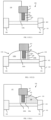
- the HBT can be symmetric and, particularly, the collector region 120 and the emitter region 140 thereof can be essentially symmetric (e.g., see the HBTs 150A and 150B of the semiconductor structures 100A and 100B of FIGs. 1A and 1B , respectively).
- the HBT can be asymmetric and, particularly, the collector region 120 and the emitter region 130 thereof can be asymmetric (e.g., see the HBTs 150C and 150D of the semiconductor structures 100C and 100D of FIGs.
- the collector region 120 can include at least one collector layer, which is immediately adjacent to the buffer layer 108a, which is selectively epitaxially and laterally grown from a sidewall of the buffer layer 108a during processing such that it is monocrystalline in structure, and which is made of a semiconductor material that has a wider (i.e., larger) bandgap than the buffer layer 108a and that further has a smaller lattice constant than the buffer layer 108a (e.g., see the collector layer 109a in collector region 120 of the symmetric HBTs 150A and 150B of the semiconductor structures 100A and 100B of FIGs. 1A and 1B ; see also the collector layer 109 in collector region 120 of the asymmetric HBTs 150C and 150D of the semiconductor structures 100C and 100C of FIGs. 1C and ID).
- the collector and emitter regions 120 and 130 can have collector and emitter layers 109a and 109b, respectively.
- These collector and emitter layers 109a and 109b can be symmetric, can be positioned laterally immediately adjacent to the buffer layers 108a and 108b, respectively, on either side of the base, can be epitaxially, selectively, and laterally grown from the buffer layers so as to be monocrystalline in structure, and can be made of a semiconductor material that has a wider (i.e., larger) bandgap and smaller lattice constant than the buffer layers.
- the base layer 105 is made of silicon germanium and the buffer layers 108a and 108b are made of silicon, aluminum phosphide, or gallium phosphide
- the collector and emitter layers 109a and 109b could be made of silicon carbide, gallium nitride, zinc oxide, aluminum nitride or any other suitable semiconductor material with a wider bandgap and smaller lattice constant that the buffer layers.
- the collector and emitter layers 109a and 109b can be relatively thin and essentially vertically-oriented and the collector and emitter regions 120 and 130 can further have additional collector and emitter layers 110a and 110b positioned laterally adjacent to the collector and emitter layers 109a and 109b, respectively.
- these additional collector and emitter layers 110a and 110b can be symmetric, can be positioned laterally immediately adjacent to the collector and emitter layers 109a and 109b, respectively, can be epitaxially, selectively, and laterally grown from the collector and emitter layers 109a and 109b so as to be monocrystalline in structure, and can be made of a semiconductor material with a narrower (i.e., smaller) bandgap than the collector and emitter layers 109a and 109b, but still a wider (i.e., larger) bandgap than the base layer 105.
- the additional collector and emitter layers 110a and 110b could be made of silicon. It should be noted that, in the symmetric HBT 150A, the additional collector and emitter layers 110a and 110b can be relatively wide and contacted (e.g., see collector/emitter contacts 118).
- the collector region 120 can have a single collector layer 109a and the emitter region 130 can have a single emitter layer 109b.
- These collector and emitter layers 109a and 109b can be symmetric, can be positioned laterally immediately adjacent to the buffer layers 108a and 108b, respectively, on either side of the base, can be epitaxially, selectively, and laterally grown from the buffer layers so as to be monocrystalline in structure, and can be made of a semiconductor material that has a wider (i.e., larger) bandgap and smaller lattice constant than the buffer layers.
- the collector and emitter layers 109a and 109b could be made of silicon carbide, gallium nitride, zinc oxide, aluminum nitride or any other suitable semiconductor material with a wider bandgap and smaller lattice constant that the buffer layers 108a and 108b. It should be noted that, in the symmetric HBT 150B, the collector and emitter layers 109a and 109b can be relatively wide and contacted (e.g., see collector/emitter contacts 118).
- the collector region 120 can include a wide bandgap material and the emitter region 130 can be devoid of any wide bandgap materials.
- the collector region 120 can include a collector layer 109.
- the collector layer 109 can be positioned laterally immediately adjacent to the buffer layer 108a, can be epitaxially, selectively, and laterally grown from the buffer layer 108a so as to be monocrystalline in structure, and can be made of a semiconductor material that has a wider (i.e., larger) bandgap and smaller lattice constant than the buffer layer 108a.
- the collector layer 109 could be made of silicon carbide, gallium nitride, zinc oxide, aluminum nitride or any other suitable semiconductor material with a wider bandgap and smaller lattice constant that the buffer layers.
- the collector layer 109 can further be relatively thin and essentially vertically-oriented and the collector region 120 can include an additional collector layer 110a.
- the additional collector layer 110a can be positioned laterally immediately adjacent to the collector layer 109, can be epitaxially, selectively, and laterally grown from the collector layer 109 so as to be monocrystalline in structure, and can be made of a semiconductor material with a narrower (i.e., smaller) bandgap than the collector layer 109, but still a wider (i.e., larger) bandgap than the base layer 105.
- the additional collector layer 110a could be made of silicon.
- the emitter region 130 can be devoid of the wide bandgap material layer and instead can include a single emitter layer 110b, which is positioned laterally immediately adjacent to the buffer layer 108b, which is epitaxially, selectively, and laterally grown from the buffer layer 108b so as to be monocrystalline in structure, and which is made of the same semiconductor material as the additional collector layer 110a.
- the additional collector layer 110a and the emitter layer 110b can be relatively wide and contacted (e.g., see collector/emitter contacts 118).
- the collector region 120 can include single wide bandgap material layer and the emitter region 130 can include a single mid bandgap material layer (i.e., can be devoid of the wide bandgap material).
- the collector region 120 can include collector layer 109.
- the collector layer 109 can be positioned laterally immediately adjacent to the buffer layer 108a, can be epitaxially, selectively, and laterally grown from the buffer layer 108a so as to be monocrystalline in structure, and can be made of a semiconductor material that has a wider (i.e., larger) bandgap and smaller lattice constant than the buffer layer 108a.
- the collector layer 109 could be made of silicon carbide, gallium nitride, zinc oxide, aluminum nitride or any other suitable semiconductor material with a wider bandgap and smaller lattice constant that the buffer layers.
- the emitter region 130 can be devoid of the wide bandgap material layer and instead can include a single emitter layer 110, which is positioned laterally immediately adjacent to the buffer layer 108b, which is epitaxially, selectively, and laterally grown from the buffer layer 108b so as to be monocrystalline in structure, and which is made of a semiconductor material with a narrower (i.e., smaller) bandgap than the collector layer 109, but still a wider (i.e., larger) bandgap than the base layer 105.
- the base layer 105 is made of silicon germanium
- the buffer layer 108b is made of silicon, aluminum phosphide, or gallium phosphide
- the collector layer 109 is made of silicon carbide, gallium nitride, zinc oxide, or aluminum nitride
- the emitter layer 110 could be made of silicon. It should be noted that, in the asymmetric HBT 150D, the collector layer 109 and the emitter layer 110 can be relatively wide and contacted (e.g., see collector/emitter contacts 118).
- collector layers 109a and 109b in the HBT 150A or 150B of FIGs. 1A and 1B or the collector layer 109 in the HBT 150C or 150D of FIGs. 1C and 1D are made of silicon carbide, then any of the different silicon carbide polytypes could be employed including, but not limited to, 3C, 4H or 6H.
- the layer or layers of the collector region 120 and emitter region 130 can have the second-type conductivity at a relatively high conductivity level.
- the collector and emitter layers can all be N+ layers; whereas, for a PNP-type HBT, the collector and emitter layers can all be P+ layers.
- the collector region 120 and the emitter region 130 are shown as being positioned above and immediately adjacent to a planar top surface of the insulator layer 102. However, it should be understood that the figures are not intended to be limiting. Alternatively, one or both of these regions 120 and 130 could fill trenches that extend partially or completely through the insulator layer 102.
- the HBT 150A-150D could include metal silicide layers 117 between the collector/emitter contacts 118 and the top surfaces of the collector and emitter regions 120 and 130 and further between the base contact 119 and the top surface of base region 140.
- the metal silicide layers 117 can be, for example, layers of cobalt silicide (CoSi), nickel silicide (NiSi), tungsten silicide (WSi), titanium silicide (TiSi), or any other suitable metal silicide material.
- the semiconductor structure 100A-100D can further include one or more dielectric layers covering the HBT. These layers can include, but are not limited to, layers of interlayer dielectric (ILD) material.
- ILD interlayer dielectric
- a first layer 112 of ILD material can cover the collector and emitter regions 120 and 130 and can further be positioned laterally adjacent to the sidewall spacers 111 (i.e., the sidewall spacers 111 can be positioned laterally between the additional base layer 114 and the first layer 112 of ILD material).
- a second layer 115 of ILD material can be on the first layer 112 and can further extend over the sidewall spacers 111 and additional base layer 114.
- the ILD material of these layers 112 and 115 can be, for example, silicon dioxide, doped silicon glass (e.g., phosphosilicate glass (PSG) or borophosphosilicate glass (BPSG)), or any other suitable ILD material.
- the base contact 119 can extend through the second layer 115 of ILD material to the optional metal silicide layer 117 on the base region 140 and the collector/emitter contacts 118 can extend through the second layer 115 and the first layer 112 of ILD material to the optional metal silicide layers 117 on the collector and emitter regions 120 and 130.
- a method for forming a semiconductor structure with a lateral heterojunction bipolar transistor such that the semiconductor structure 100A with the lateral symmetric HBT 150A of FIG. 1A , the semiconductor structure 100B with the lateral symmetric HBT 150B of FIG. 1B , the semiconductor structure 100C with the lateral asymmetric HBT 150C of FIG. 1C , or the semiconductor structure 100D with the lateral asymmetric HBT 150D of FIG. 1D .
- HBT heterojunction bipolar transistor
- the method can begin with accessing an initial semiconductor-on-insulator structure (e.g., a silicon-on-insulator (SOI) structure) (see process 202 and FIG. 3 ).
- the initial semiconductor-on-insulator structure can include a semiconductor substrate 101.
- the semiconductor substrate 101 can be, for example, a silicon substrate that is monocrystalline in structure.
- the semiconductor substrate 101 can be doped so as to have P-type conductivity at a relatively low conductivity level.
- the semiconductor substrate 101 could be a P- silicon substrate.
- the initial semiconductor-on-insulator structure can further include an insulator layer 102 on the top surface of the semiconductor substrate 101.
- the insulator layer 102 can be, for example, a silicon dioxide layer (also referred to herein as a buried oxide (BOX) layer) or a layer of any other suitable insulator material.
- the initial semiconductor-on-insulator structure can further include a semiconductor layer 103 on the insulator layer 102.
- the semiconductor layer 103 can be, for example, a silicon layer that is monocrystalline in structure.
- the semiconductor layer 103 of the initial semiconductor-on-insulator initial structure will be used during subsequent processing (see process 210) as a seed layer for epitaxial growth of a base layer (e.g., a silicon germanium base layer) for an HBT.
- a seed layer need only be a few nanometers thick (e.g., 1-5nm).
- the method can optionally include thinning the semiconductor layer 103 (see process 204 and FIG. 4 ).
- Various different techniques for thinning a semiconductor layer are known in the art and can be employed at process 204.
- One exemplary technique can include oxidizing the upper portion of the semiconductor layer to form an oxide layer (i.e., a silicon dioxide layer) and subsequently selectively removing the resulting oxide layer (e.g., using a buffered hydrofluoric acid (HF) wet etch technique or some other suitable technique for selectively etching silicon dioxide without etching the silicon material below).
- oxide layer i.e., a silicon dioxide layer
- HF buffered hydrofluoric acid
- the method can further include forming a transistor and, particularly, a lateral heterojunction bipolar transistor (HBT) (e.g., such as any of the HBTs 150A-150D described above) using the seed layer 103 (see process 206).
- HBT lateral heterojunction bipolar transistor
- the HBT formed at process 206 can be an NPN-type HBT or, alternatively, a PNP-type HBT.
- the first-type conductivity and the second-type conductivity are either P-type conductivity and N-type conductivity, respectively, or N-type conductivity and P-type conductivity, respectively, depending upon whether the HBT is an NPN-type HBT or a PNP-type HBT.
- the first-type conductivity refers to P-type conductivity
- the second-type conductivity refers to N-type conductivity.
- the HBT is a PNP-type HBT
- the first-type conductivity refers to N-type conductivity
- the second-type conductivity refers to P-type conductivity. See the detailed discussion below regarding different dopants that can be employed in semiconductor materials to achieve P-type conductivity or N-type conductivity.
- a base layer 105 can be formed on the seed layer 103 (see process 210 and FIG. 5 ).
- the base layer 105 can be formed at process 210, for example, using a selective epitaxially growth process such that it is monocrystalline in structure.
- the semiconductor material of the base layer 105 can be selected such that it has a relatively narrow (i.e., small) bandgap as compared to, for example, silicon.
- the base layer 105 can be, for example, a monocrystalline epitaxial silicon germanium layer.
- the base layer 105 can be either undoped or in situ doped during epitaxial deposition so as to have the first-type conductivity.
- the base layer 105 can be undoped (i.e., an intrinsic base layer).
- the base layer 105 can be in situ doped at process 210 so as to have P-type conductivity at a relatively low conductivity level (i.e., a P- base layer), so as to have a graded P-type profile (e.g., from undoped or P- at the bottom surface near the seed layer 103 to P or P+ at the top surface), or so as to have P-type conductivity at a relatively high conductivity level (i.e., a P+ base layer).
- the base layer 105 can be undoped (i.e., an intrinsic base layer).
- the base layer 105 can be in situ doped at process 210 so as to have N-type conductivity at a relatively low conductivity level (i.e., an N- base layer), so as to have a graded N-type profile (e.g., from undoped or N- at the bottom surface near the seed layer 103 to N or N+ at the top surface), or so as to have N-type conductivity at a relatively high conductivity level (i.e., a N+ base layer).
- Shallow trench isolation (STI) regions 106 can be formed using conventional STI formation techniques to define the HBT device area (see process 212 and FIG. 6 ). Specifically, at process 212, trenches can be formed (e.g., lithographically patterned and etched) such that the extend vertically through the base layer 105, through the seed layer 103 and, optionally, through insulator layer 102 and into the substrate 101 below. One or more layers of isolation material (e.g., silicon dioxide, silicon nitride, silicon oxynitride or any other suitable isolation material) can subsequently be deposited so as to fill the trench. A polishing process (e.g., a chemical mechanical polishing (CMP) process can then be performed so as to remove all isolation materials from above the base layer 105.
- CMP chemical mechanical polishing
- a mask layer (e.g., a silicon nitride hardmask layer or some other suitable hardmask layer) can be formed over the base layer 105 and adjacent STI regions 106 (see process 214).
- the mask layer can subsequently be lithographically patterned and etched such that the remaining portion of the mask layer (referred to herein as a base mask 107) is on the base layer 105 (e.g., at approximately the center of the HBT device area) (see process 214 and FIG. 7 ).
- Process 216 can be performed using one or more anisotropic etch processes that is/are selective for the semiconductor materials of the base layer 105 and seed layer 103 over the adjacent isolation materials.
- anisotropic etch processes that is/are selective for the semiconductor materials of the base layer 105 and seed layer 103 over the adjacent isolation materials.
- Various different techniques for selectively and anisotropically etching semiconductor materials are known in the art and could be employed at process 216. For example, a potassium hydroxide (KOH) wet etch process could be employed to selectively and anisotropically etch both a silicon germanium base layer and a silicon seed layer below.
- KOH potassium hydroxide
- this etch process is illustrated in FIG. 8 as stopping on the top surface of the insulator layer 102.
- the figures are not intended to be limiting.
- processing can be performed so that the isolation layer is also partially or even completely etched through on one or both sides of the base stack.
- the opposing sidewalls of the base stack can be etched back, thereby reducing the width of the base stack (see process 218 and FIG. 9 ).
- the sidewalls of the base stack could be oxidized, thereby forming an oxide layer. Then, the oxide layer could be selectively removed. It should be understood that, if the insulator layer 102 is an oxide layer, it would also be etched to some extent.
- a selective isotropic etch process e.g., a dry chemical etch process
- a selective isotropic etch process could be performed to etch back the sidewalls of the base stack.
- Thin buffer layers 108a-108b can subsequently be formed so as to cover the opposing sidewalls of base stack (see process 220 and FIG. 10 ).
- the buffer layers 108a and 108b can be concurrently selectively epitaxially grown from the opposing sidewalls of the base layer 105-seed layer 103 stack (or otherwise formed, such as by chemical vapor deposition) such that they are monocrystalline in structure.
- the semiconductor material of the buffer layers 108a and 108b can specifically be selected at process 220 so as to have a wider (i.e., larger) bandgap than the base layer 105, but so as to also have an equal or approximately equal lattice constant.
- the semiconductor material of the buffer layers 108a and 108b could be silicon, aluminum phosphide, gallium phosphide, or any other suitable semiconductor material with a larger bandgap but similar lattice constant as compared to silicon germanium.
- the buffer layers 108a and 108b can be in situ doped so as to have a second-type conductivity, which is different from the first-type conductivity and which is at a relatively low conductivity level.
- the buffer layers 108a and 108b can be in situ doped so as to be N- buffer layers (e.g., effectively forming N- collector/emitter extension regions); whereas, for a PNP-type HBT, the buffer layers 108a and 108b can be in situ doped so as to be P- buffer layers (e.g., effectively forming P- collector/emitter extension regions).
- the method can further include forming a collector region 120 and an emitter region 130 such that the base layer 105 is positioned laterally between the collector region 120 and the emitter region 130 and further such that at least the collector region 120 include a wide bandgap semiconductor material layer positioned laterally immediately adjacent to the buffer layer 108a (see process 222).
- the techniques used to form the collector region 120 and the emitter region 130 will vary depending upon the semiconductor structure being formed. For example, process steps for forming the emitter region 130 and the collector region 120 can be performed concurrently if the HBT is to be symmetric as illustrated in FIGs. 1A and 1B .
- the process steps for forming the emitter region 130 and the collector region 120 can be performed sequentially so that the resulting HBT can be asymmetric as illustrated in FIGs. 1C and 1D .
- Process steps can also vary depending upon whether the collector region 120 will have two collector layers as illustrated in FIGs. 1A and 1C or a single collector layer as illustrated in FIGs. 1B and 1D .
- collector and emitter layers 109a and 109b can be epitaxially, selectively, and laterally grown from the buffer layers 108a and 108b, respectively, such that they are monocrystalline in structure (see FIG. 11A(1) ).
- the collector and emitter layers 109a and 109b can be made of a semiconductor material that has a wider (i.e., larger) bandgap and smaller lattice constant than the buffer layers.
- the collector and emitter layers 109a and 109b could be made of silicon carbide, gallium nitride, zinc oxide, aluminum nitride or any other suitable semiconductor material with a wider bandgap and smaller lattice constant that the buffer layers.
- the collector and emitter layers 109a and 109b can be relatively thin and essentially vertically-oriented.
- additional collector and emitter layers 110a and 110b can be epitaxially, selectively, and laterally grown from the collector and emitter layers 109a and 109b such that they are also monocrystalline in structure (see FIG. 11A(2) ).
- the additional collector and emitter layers 110a and 110b can be made of a semiconductor material with a narrower (i.e., smaller) bandgap than the collector and emitter layers 109a and 109b, but still a wider (i.e., larger) bandgap than the base layer 105.
- the base layer 105 is made of silicon germanium
- the buffer layers 108a and 108b are made of silicon, aluminum phosphide, or gallium phosphide
- the collector and emitter layers 109a and 109b are made of silicon carbide, gallium nitride, zinc oxide, or aluminum nitride
- the additional collector and emitter layers 110a and 110b could be made of silicon.
- both the collector region and the emitter region include a wide bandgap semiconductor material layer.
- the additional collector and emitter layers 110a and 110b can be formed so that they are relatively wide as compared to the collector and emitter layers 109a and 109b, so that they fill the space between the collector and emitter layers and the adjacent STI regions, and so that they can subsequently be contacted.
- collector and emitter regions 120 and 130 of the symmetric HBT 150B in the semiconductor structure 100B of FIG. 1B relatively wide collector and emitter layers 109a and 109b can be epitaxially, selectively, and laterally grown from the buffer layers 108a and 108b so that they are monocrystalline in structure (see FIG. 11B ).
- the collector and emitter regions each only contain a single semiconductor layer.
- the collector and the emitter layers 109a and 109b can be made of a semiconductor material that has a wider (i.e., larger) bandgap and smaller lattice constant than the buffer layers.
- the collector and emitter layers 109a and 109b could be made of silicon carbide, gallium nitride, zinc oxide, aluminum nitride or any other suitable semiconductor material with a wider bandgap and smaller lattice constant that the buffer layers 108a and 108b.
- both the collector region and the emitter region include a wide bandgap semiconductor material layer. It should be noted that in this case the collector and emitter layers 109a and 109b can be formed so that they are relatively wide, so that they extend to the adjacent STI regions, and so that they can be contacted during subsequent processing.
- a protective layer 199 can be formed in the designated emitter area so as to cover emitter-side sidewall of the base stack and leave the collector-side sidewall of the base stack exposed (see FIG. 11C(1) .
- a collector layer 109 for the collector region 120 can be epitaxially, selectively, and laterally grown from the buffer layer 108a such that it is monocrystalline in structure (see FIG. 11C(1) ).
- the collector layer 109 can be made of a semiconductor material that has a wider (i.e., larger) bandgap and smaller lattice constant than the buffer layer 108a.
- the collector layer 109 could be made of silicon carbide, gallium nitride, zinc oxide, aluminum nitride or any other suitable semiconductor material with a wider bandgap and smaller lattice constant that the buffer layers.
- the collector layer 109 can further be relatively thin and essentially vertically-oriented.
- the protective layer 199 can then be selectively removed and an additional collector layer 110a for the collector region 120 and an emitter layer 110b for the emitter region 130 can be epitaxially, selectively, and laterally grown from the collector layer 109 and buffer layer 108b, respectively, so that these layers are monocrystalline in structure (see FIG. 11C(2) ).
- the emitter layer 110 and the additional collector layer 109b can be made of a semiconductor material with a narrower (i.e., smaller) bandgap than the collector layer 109, but still a wider (i.e., larger) bandgap than the base layer 105.
- the base layer 105 is made of silicon germanium
- the buffer layers 108a and 108b are made of silicon, aluminum phosphide, or gallium phosphide
- the collector layer 109 is made of silicon carbide, gallium nitride, zinc oxide, or aluminum nitride
- the additional collector layer 110a and the emitter layer 110b could be made of silicon.
- the emitter region 130 is devoid of the wide bandgap material layer.
- the additional collector layer 109b and emitter layer 110 can be formed so that they are relatively wide, so that they extend to the adjacent STI regions, and so that they can be contacted during subsequent processing.
- a protective layer 198 can be formed in the designated emitter area so as to cover emitter-side sidewall of the base stack and so as to leave the collector-side sidewall of the base stack exposed (see FIG. 11D(1) ).
- a collector layer 109 for the collector region 120 can be epitaxially, selectively, and laterally grown from the buffer layer 108a such that it is monocrystalline in structure (see FIG. 11D(1) ).
- the collector layer 109 can be made of a semiconductor material that has a wider (i.e., larger) bandgap and smaller lattice constant than the buffer layer 108a.
- the collector layer 109 could be made of silicon carbide, gallium nitride, zinc oxide, aluminum nitride or any other suitable semiconductor material with a wider bandgap and smaller lattice constant that the buffer layers.
- the collector layer 109 can be formed so that it is relatively wide, so that that it extends to the adjacent STI region, and so that it can be contacted during subsequent processing.
- an emitter layer 110 can be epitaxially, selectively, and laterally grown from the buffer layer 108b such that it is monocrystalline in structure (see FIG. 11D(2) ).
- the emitter layer 110 can be made of a semiconductor material with a narrower (i.e., smaller) bandgap than the collector layer 109, but still a wider (i.e., larger) bandgap than the base layer 105.
- the base layer 105 is made of silicon germanium
- the buffer layers 108a and 108b are made of silicon, aluminum phosphide, or gallium phosphide
- the collector layer 109 is made of silicon carbide, gallium nitride, zinc oxide, or aluminum nitride
- the emitter layer 110 could be made of silicon.
- the protective layer 196 can be selective removed (see FIG. 11D(3) ).
- the emitter region 130 is devoid of the wide bandgap material layer.
- the collector layer 109 and emitter layer 110 can be formed so that they are relatively wide, so that they extend to the adjacent STI regions, and so that they can be contacted during subsequent processing.
- the layer or layers of the collector region 120 and emitter region 130 which are epitaxially deposited at process 222 as described above, can be in situ doped so as to have the second-type conductivity at a relatively high conductivity level.
- the collector and emitter layers can all be in N+ layers; whereas, for a PNP-type HBT, the collector and emitter layers can all be P+ layers.
- a first layer 112 of interlayer dielectric (ILD) material can be deposited so as to cover the collector region 120, the base mask 107, and the emitter region 130 (see process 224 and FIG. 12 ).
- the ILD material of the layer 112 can be, for example, silicon dioxide, doped silicon glass (e.g., phosphosilicate glass (PSG) or borophosphosilicate glass (BPSG)), or any other suitable ILD material.
- This first layer 112 can then be polished (e.g., using a CMP process) to expose the top surface of the base mask 107 (see process 226 and FIG. 12 ). The exposed base mask 107 can then be selectively removed (see process 228 and FIG. 13 ).
- the ILD material of layer 112 should be different from the hard mask material (e.g., silicon nitride) of the base mask 107 so that this base mask can be selectively removed using, for example, a plasma etch or other suitable selective etch process.
- removal of the base mask 107 creates an extrinsic base opening 113 aligned above the base layer 105 and extending laterally over at least a portion of the adjacent buffer layers 108a and 108b.
- the width of this extrinsic base opening 113 can be narrowed by the formation of sidewalls spacers 111 (see process 230 and FIG. 14 ).
- a dielectric sidewall spacer material layer can be deposited (e.g., conformally) over the partially completed structure so as to line the extrinsic base opening 113.
- the dielectric sidewall spacer material layer can be, for example, a silicon nitride layer, a silicon carbon nitride layer, a silicon boron carbon nitride layer or any other suitable dielectric sidewall spacer material layer.
- a selective anisotropic etch process can be performed so as to remove horizontal portions of the dielectric sidewall spacer material layer, leaving essentially vertical portions intact within the extrinsic base opening 113 as sidewall spacers 111.
- An additional base layer 114 (also referred to herein as an extrinsic base layer) can subsequently be formed (e.g., epitaxially grown) in the extrinsic base opening 113 above and immediately adjacent to the base layer 105 and positioned laterally between and immediately adjacent to the sidewall spacers 111 (see process 232 and FIG. 15 ).
- This additional base layer 114 can be selectively grown at process 232 from the top surface of the base layer 105 only during processing such that it is monocrystalline in structure.
- this additional base layer 114 can be non-selectively grown at process 232 from both the top surface of the base layer 105 and from the sidewall spacers such that it is polycrystalline in structure.
- the additional base layer 114 can be made of the same semiconductor material as the base layer 105 (e.g., silicon germanium) such that it too has a relatively narrow bandgap as compared to, for example, silicon.
- the additional base layer 114 can be made of a different semiconductor material that the base layer 105 (e.g., silicon).
- the additional base layer 114 can be in situ doped so as to have the first-type conductivity at a relatively high conductivity level.
- the additional base layer 114 can be a P+ base layer; whereas, for a PNP-type HBT, the additional base layer 114 can be an N+ base layer.
- a second layer 115 of ILD material can be formed on the first layer 112 and extending over the sidewall spacers 111 and additional base layer 114 (see process 234 and FIG. 16 ).
- the second layer 115 can be made of the same ILD material as the first layer 112 or, alternatively, a different ILD material. That is, the ILD material of the second layer 115 can be any of silicon dioxide, doped silicon glass (e.g., phosphosilicate glass (PSG) or borophosphosilicate glass (BPSG)), or any other suitable ILD material.
- PSG phosphosilicate glass
- BPSG borophosphosilicate glass
- Contact openings 116 can subsequently be formed (e.g., patterned and etched) (see process 236 and FIG. 17 ).
- the contact openings 116 can include a base contact opening that extends through the second layer 115 of ILD material to the top surface of the base region 140 and collector/emitter contact openings that extend through the second layer 115 and the first layer 112 of ILD material to the collector and emitter regions 120 and 130.
- metal silicide layer 117 can be formed on exposed surfaces of the collector region 120, base region 140 and emitter region 130 at the bottom of the contact openings (e.g., using a self-aligned silicide formation process, also referred to herein as a salicide formation process) (see process 238 and FIG. 18 ).
- the metal silicide layers 117 can be, for example, layers of cobalt silicide (CoSi), nickel silicide (NiSi), tungsten silicide (WSi), titanium silicide (TiSi), or any other suitable metal silicide material.
- CoSi cobalt silicide
- NiSi nickel silicide
- WSi tungsten silicide
- TiSi titanium silicide
- conventional middle-of-the-line (MOL) contacts can be formed including a base contact 119 in the base contact opening and collector/emitter contacts 118 in the collector/emitter contact openings (see process 240 and FIG. 19 ).
- a semiconductor material refers to a material whose conducting properties can be altered by doping with an impurity.
- Exemplary semiconductor materials include, for example, silicon-based semiconductor materials (e.g., silicon, silicon germanium, silicon germanium carbide, silicon carbide, etc.) and III-V compound semiconductors (i.e., compounds obtained by combining group III elements, such as aluminum (Al), gallium (Ga), or indium (In), with group V elements, such as nitrogen (N), phosphorous (P), arsenic (As) or antimony (Sb)) (e.g., GaN, InP, GaAs, or GaP).
- group III elements such as aluminum (Al), gallium (Ga), or indium (In)
- group V elements such as nitrogen (N), phosphorous (P), arsenic (As) or antimony (Sb)
- group III elements such as aluminum (Al), gallium (Ga), or indium (In)
- group V elements such as nitrogen (N), phospho
- a pure semiconductor material and, more particularly, a semiconductor material that is not doped with an impurity for the purposes of increasing conductivity is referred to in the art as an intrinsic semiconductor.
- a semiconductor material that is doped with an impurity for the purposes of increasing conductivity is referred to in the art as an extrinsic semiconductor and will be more conductive than an intrinsic semiconductor made of the same base material. That is, extrinsic silicon will be more conductive than intrinsic silicon; extrinsic silicon germanium will be more conductive than intrinsic silicon germanium; and so on.
- a silicon-based semiconductor material e.g., silicon, silicon germanium, etc.
- a Group III dopant such as boron (B) or indium (In)
- a silicon-based semiconductor material is typically doped a Group V dopant, such as arsenic (As), phosphorous (P) or antimony (Sb), to achieve N-type conductivity.
- a gallium nitride (GaN)-based semiconductor material is typically doped with magnesium (Mg) to achieve P-type conductivity and with silicon (Si) or oxygen to achieve N-type conductivity.
- Mg magnesium
- Si silicon
- oxygen oxygen
- the method as described above is used in the fabrication of integrated circuit chips.
- the resulting integrated circuit chips can be distributed by the fabricator in raw wafer form (that is, as a single wafer that has multiple unpackaged chips), as a bare die, or in a packaged form.
- the chip is mounted in a single chip package (such as a plastic carrier, with leads that are affixed to a motherboard or other higher level carrier) or in a multichip package (such as a ceramic carrier that has either or both surface interconnections or buried interconnections).
- the chip is then integrated with other chips, discrete circuit elements, and/or other signal processing devices as part of either (a) an intermediate product, such as a motherboard, or (b) an end product.
- the end product can be any product that includes integrated circuit chips, ranging from toys and other low-end applications to advanced computer products having a display, a keyboard or other input device, and a central processor.
- laterally is used herein to describe the relative locations of elements and, more particularly, to indicate that an element is positioned to the side of another element as opposed to above or below the other element, as those elements are oriented and illustrated in the drawings.
- an element that is positioned laterally adjacent to another element will be beside the other element
- an element that is positioned laterally immediately adjacent to another element will be directly beside the other element
- an element that laterally surrounds another element will be adjacent to and border the outer sidewalls of the other element.
Landscapes
- Bipolar Transistors (AREA)
Abstract
A structure comprises: a base region (140) comprising a base layer (105); a buffer layer (108a) positioned laterally immediately adjacent to the base layer; and a collector region (120) comprising a collector layer (109a) positioned laterally immediately adjacent to the buffer layer, wherein the base layer, the buffer layer, and the collector layer comprise different semiconductor materials with different bandgap sizes.
Description
- The present invention relates semiconductor structures and methods of forming semiconductor structures.
- Advantages associated with manufacturing complementary metal oxide semiconductor (CMOS) designs using advanced silicon-on-insulator (SOI) processing technology platforms (e.g., a fully-depleted silicon-on-insulator (FDSOI) processing technology platform) include, for example, reduced power, reduced area consumption, reduced cost, high performance, multiple core threshold voltage (Vt) options, etc. CMOS designs manufactured on such SOI wafers are used in a variety of applications including, but not limited to, Intemet-of-Things (IOT) devices, wearable devices, smartphone processors, automotive electronics, and radio frequency integrated circuits (RFICs) (including millimeter wave (mmWave) ICs). These same applications could benefit from the inclusion of bipolar junction transistors (BJTs) because BJTs tend to have more drive and are generally considered better suited for analog functions than field effect transistors (FETs). However, BJTs are typically formed as vertical devices (e.g., with an in-substrate collector, a base aligned above the collector, and an emitter aligned above the base) and such vertical BJTs are not easily incorporated into advanced SOI processing technology platforms. Recently, lateral BJTs have been developed that can be incorporated into advanced SOI technology platforms along with CMOS devices but at the expense of performance (e.g., low cut-off frequency (fT)/maximum oscillation frequency (fmax) and beta cut-off frequency, low breakdown voltage (BV), etc.).
- Disclosed herein are embodiments of a semiconductor structure. The semiconductor structure can include a base region. The base region can include a base layer. The semiconductor structure can further include a buffer layer, which is positioned laterally immediately adjacent to the base layer. The semiconductor structure can further include a collector region, which includes a collector layer positioned laterally immediately adjacent to the buffer layer. In this semiconductor structure the base layer, the buffer layer, and the collector layer can be made of different semiconductor materials with different bandgap sizes.
- Some embodiments of a semiconductor structure disclosed here can specifically include a multi-layered collector region. For example, the semiconductor structure can include a base region. The base region can include a base layer. The semiconductor structure can further include a buffer layer, which is positioned laterally immediately adjacent to the base layer. The semiconductor structure can further include a collector region, which includes a collector layer positioned laterally immediately adjacent to the buffer layer and an additional collector layer positioned laterally immediately adjacent to the collector layer. In this semiconductor structure the base layer, the buffer layer, and the collector layer can also be made of different semiconductor materials with different bandgap sizes.
- Also disclosed herein are embodiments of a method for forming the above-described semiconductor structure. The method can include forming a base region that includes a base layer. The method can further include forming buffer layer such that it is positioned laterally immediately adjacent to the base layer. The method can further include forming a collector region that includes a collector layer positioned laterally immediately adjacent to the buffer layer. Additionally, in the method, the processes of forming the base region, forming the buffer layer and forming the collector region can be performed such that the base layer, the buffer layer, and the collector layer are made of different semiconductor materials with different bandgap sizes.
- The present invention will be better understood from the following detailed description with reference to the drawings, which are not necessarily drawn to scale and in which:
-
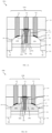
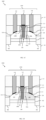
FIGs. 1A-1D are cross-section diagrams illustrating different embodiments of a semiconductor structure including a lateral heterojunction bipolar transistor (HBT) configured for improved performance; -
FIG. 2 is a flow diagram illustrating method embodiments for forming the semiconductor structures shown inFIGs. 1A-1D ; -
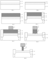
FIGs. 3-10 are cross-section diagrams illustrating partially completed semiconductor structures formed according to the flow diagram ofFIG. 2 during manufacture of any of the structures shown inFIGs. 1A-1D ; -
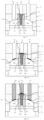
FIGs. 11A(1)-11A(2) are cross-section diagrams illustrating partially completed semiconductor structures formed at process 222 specifically during manufacture of the structureFIG. 1A ; -
FIG. 11B is cross-section diagram illustrating a partially completed semiconductor structure formed at process 222 specifically during manufacture of the structure shown inFIG. 1B ; -
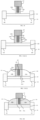
FIGs. 11C(1)-11C(2) are cross-section diagrams illustrating partially completed semiconductor structures formed at process 222 specifically during manufacture of the structure shown inFIG. 1C ; and -
FIGs. 11D(1)-11D(3) are cross-section diagrams illustrating partially completed semiconductor structures formed at process 222 specifically during manufacture of the structure shown in FIG. ID; and -
FIGs. 12-19 are cross-section diagrams illustrating partially completed semiconductor structures illustrating the remaining processes of the flow diagram ofFIG. 2 (e.g., with respect to the structure shown inFIG. 1A . - As mentioned above, lateral bipolar junction transistors (BJTs) have been developed that can be incorporated into advanced silicon-on-insulator (SOI) technology platforms along with complementary metal oxide semiconductor (CMOS devices) but at the expense of performance (e.g., low cut-off frequency (fT)/maximum oscillation frequency (fmax) and beta cut-off frequency, low breakdown voltage (BV), etc.).
- In view of the foregoing, disclosed herein are embodiments of a semiconductor structure including a device, such as a lateral heterojunction bipolar transistor (HBT), made up of a combination of at least three different semiconductor materials with different bandgap sizes, respectively, for improved performance (e.g., to increase cut-off frequency (fT)/maximum oscillation frequency (fmax) and beta cut-off frequency and to increase breakdown voltage (BV)). In the device, a base layer of a base region can be positioned laterally between a collector layer of a collector region and an emitter layer of an emitter region and can be physically separated therefrom by buffer layers. The base layer can be made of a narrow bandgap semiconductor material, the collector layer and, optionally, the emitter layer can be made of a wide bandgap semiconductor material, and the buffer layers can be made of another semiconductor material with a medium bandgap between that of the narrow bandgap semiconductor material and the wide bandgap semiconductor material. Also disclosed herein are method embodiments for forming the semiconductor structure.
- More specifically, referring to
FIGs. 1A-1D , disclosed herein are embodiments of a semiconductor structure 100A-100D, respectively. The semiconductor structure 100A-100D can be, for example, a semiconductor-on-insulator structure (e.g., a silicon-on-insulator (SOI) structure). That is, the semiconductor structure 100A-100D can include asemiconductor substrate 101. Thesemiconductor substrate 101 can be, for example, a silicon substrate that is monocrystalline in structure. Optionally, thesemiconductor substrate 101 can be doped so as to have P-type conductivity at a relatively low conductivity level. Thus, for example, thesemiconductor substrate 101 could be a P- silicon substrate. Optionally, thesemiconductor substrate 101 can include a buried well (not shown, also referred to as a buried dopant implant region). The buried well could be doped so as to have P-type conductivity (e.g., so as to be a buried Pwell). Alternatively, the buried well could be doped so as to have N-type conductivity (e.g., so as to be a buried Nwell). - The semiconductor structure 100A-100D can further include an
insulator layer 102 on the top surface of thesemiconductor substrate 101. Theinsulator layer 102 can be, for example, a silicon dioxide layer (also referred to herein as a buried oxide (BOX) layer) or a layer of any other suitable insulator material. - The semiconductor structure 100A-100D can further include a semiconductor layer on the
insulator layer 102. The semiconductor layer can be, for example, a silicon layer that is monocrystalline in structure. The semiconductor structure 100A-100D can further include isolation structures (e.g., shallow trench isolation (STI) regions 106)) that extend vertically through the semiconductor layer and to or, optionally, through theinsulator layer 102 so as to define an active device region. - The semiconductor structure 100A-100D can further include a transistor and, particularly, a lateral heterojunction bipolar transistor (HBT) 150A-150D, respectively, in the active device region. Those skilled in the art will recognize that, like a conventional bipolar junction transistor (BJT), an HBT includes a base region with one type conductivity between an emitter region and a collector region with another type conductivity. However, instead of using the same semiconductor material for all three regions, in an HBT different semiconductor materials are used for the emitter-base junction and the base-collector junction. Those skilled in the art will recognize that an HBT is generally considered able to handle higher frequency operations than a BJT.
- The
HBT 150A-150D can be an NPN-type HBT or, alternatively, a PNP-type HBT. In the below description of the HBT, reference is made to semiconductor layers and/or regions being doped so as to have a first-type conductivity or a second-type conductivity that is different from the first-type conductivity. It should be understood that the first-type conductivity and the second-type conductivity are either P-type conductivity and N-type conductivity, respectively, or N-type conductivity and P-type conductivity, respectively, depending upon whether the HBT is an NPN-type HBT or a PNP-type HBT. Specifically, if the HBT is an NPN-type HBT, then the first-type conductivity refers to P-type conductivity and the second-type conductivity refers to N-type conductivity. However, if the HBT is a PNP-type HBT, then the first-type conductivity refers to N-type conductivity and the second-type conductivity refers to P-type conductivity. See the detailed discussion below regarding different dopants that can be employed in semiconductor materials to achieve P-type conductivity or N-type conductivity. - In any case, the
HBT 150A-150D can include abase region 140. Thebase region 140 can include a relatively thin and narrow section of the semiconductor layer on the insulator layer 102 (referred to herein as the seed layer 103). Thisseed layer 103 can be doped so as to have a first-type conductivity at a relatively low conductivity level. For example, theseed layer 103 can be a P- seed layer in the case of an NPN-type HBT or an N- seed layer in the case of a PNP-type HBT. - The
base region 140 including abase layer 105 above and immediately adjacent to the seed layer 103 (i.e., on but separated from theinsulator layer 102 by the seed layer 103). Thisbase layer 105 can be a semiconductor layer, which has been selectively epitaxially grown from theseed layer 103 during processing such that it is monocrystalline in structure. Thebase layer 105 can be made of a semiconductor material with a relatively narrow (i.e., small) bandgap as compared to, for example, silicon. Thus, thebase layer 105 can be, for example, a monocrystalline silicon germanium layer. Thebase layer 105 can be undoped or, alternatively, doped so as to have the first-type conductivity. For example, for an NPN-type HBT, thebase layer 105 can be undoped (i.e., an intrinsic base layer). Alternatively, for an NPN-type HBT, thebase layer 105 can be doped so as to have P-type conductivity at a relatively low conductivity level (i.e., a P- base layer), so as to have a graded P-type profile (e.g., from undoped or P- at the bottom surface near theseed layer 103 to P or P+ at the top surface), or so as to have P-type conductivity at a relatively high conductivity level (i.e., a P+ base layer). Similarly, for a PNP-type HBT, thebase layer 105 can be undoped (i.e., an intrinsic base layer). Alternatively, for a PNP-type HBT, thebase layer 105 can be doped so as to have N-type conductivity at a relatively low conductivity level (i.e., an N- base layer), so as to have a graded N-type profile (e.g., from undoped or N- at the bottom surface near theseed layer 103 to N or N+ at the top surface), or so as to have N-type conductivity at a relatively high conductivity level (i.e., a N+ base layer). As discussed in greater detail below, thebase layer 105 can be positioned laterally between acollector region 120 and anemitter region 130 and further separated therefrom by buffer layers (i.e., a collector-side buffer layer 108a and an emitter-side buffer layer 108b). - The
base region 140 can further include an additional base layer 114 (also referred to herein as an extrinsic base layer) above and immediately adjacent to thebase layer 105. Thisadditional base layer 114 can be another semiconductor layer, which has been either selectively or non-selectively epitaxially grown during processing such that it is either monocrystalline or polycrystalline in structure (as discussed further below with regard to the method). Theadditional base layer 114 can be made of the same semiconductor material as the base layer 105 (e.g., silicon germanium) such that it too has a relatively narrow bandgap as compared to, for example, silicon. Alternatively, theadditional base layer 114 can be made of a different semiconductor material that the base layer 105 (e.g., silicon). - In any case, the
additional base layer 114 can be doped so as to have the first-type conductivity at a relatively high conductivity level. For example, for an NPN-type HBT, theadditional base layer 114 can be a P+ base layer; whereas, for a PNP-type HBT, theadditional base layer 114 can be an N+ base layer. Theadditional base layer 114 can be contacted (e.g., see base contact 119). Theadditional base layer 114 can be positioned laterally betweendielectric sidewall spacers 111, which are on thebuffer layers 108a-108b and which can optionally extend laterally onto theemitter region 130 andcollector region 120. Thedielectric sidewall spacers 111 can be made, for example, of silicon nitride, silicon carbon nitride, silicon boron carbon nitride or any other suitable sidewall spacer material. - As mentioned above, the
base layer 105 can be positioned laterally between acollector region 120 and anemitter region 130 and further separated therefrom by buffer layers (i.e., a collector-side buffer layer 108a and an emitter-side buffer layer 108b). More specifically, the base layer 105-seed layer 103 stack can have an essentially uniform width with opposing sidewalls. TheHBT 150A-150D can further include relativelythin buffer layers 108a-108b covering the opposing sidewalls of this stack so that theseed layer 103 is positioned laterally between and immediately adjacent to thebuffer layers base layer 105 is positioned laterally between and immediately adjacent to thebuffer layers seed layer 103 stack during processing such that they are monocrystalline in structure. The semiconductor material of thebuffer layers base layer 105, but so as to also have an equal or approximately equal lattice constant to that of thebase layer 105. Thus, for example, if thebase layer 105 is a silicon germanium layer, then the semiconductor material of thebuffer layers buffer layers buffer layers buffer layers buffer layers - In each of the embodiments, the
collector region 120 can be positioned laterally adjacent to thebuffer layer 108a and theemitter region 130 can be positioned laterally adjacent to thebuffer layer 108b. As discussed in greater detail below, in some embodiments, the HBT can be symmetric and, particularly, thecollector region 120 and theemitter region 140 thereof can be essentially symmetric (e.g., see theHBTs semiconductor structures 100A and 100B ofFIGs. 1A and 1B , respectively). In other embodiments, the HBT can be asymmetric and, particularly, thecollector region 120 and theemitter region 130 thereof can be asymmetric (e.g., see theHBTs semiconductor structures 100C and 100D ofFIGs. 1C and 1D , respectively). In any case, in each of the embodiments, thecollector region 120 can include at least one collector layer, which is immediately adjacent to thebuffer layer 108a, which is selectively epitaxially and laterally grown from a sidewall of thebuffer layer 108a during processing such that it is monocrystalline in structure, and which is made of a semiconductor material that has a wider (i.e., larger) bandgap than thebuffer layer 108a and that further has a smaller lattice constant than thebuffer layer 108a (e.g., see thecollector layer 109a incollector region 120 of thesymmetric HBTs semiconductor structures 100A and 100B ofFIGs. 1A and 1B ; see also thecollector layer 109 incollector region 120 of theasymmetric HBTs semiconductor structures FIGs. 1C and ID). - More specifically, in the
symmetric HBT 150A in the semiconductor structure 100A ofFIG. 1A , the collector andemitter regions emitter layers emitter layers buffer layers base layer 105 is made of silicon germanium and thebuffer layers emitter layers symmetric HBT 150A in the semiconductor structure 100A ofFIG. 1A , the collector andemitter layers emitter regions emitter layers emitter layers emitter layers emitter layers emitter layers emitter layers base layer 105. Thus, for example, if thebase layer 105 is made of silicon germanium, thebuffer layers emitter layers emitter layers symmetric HBT 150A, the additional collector andemitter layers - Alternatively, in the
symmetric HBT 150B in thesemiconductor structure 100B ofFIG. 1B , thecollector region 120 can have asingle collector layer 109a and theemitter region 130 can have asingle emitter layer 109b. These collector andemitter layers buffer layers base layer 105 is made of silicon germanium and thebuffer layers emitter layers buffer layers symmetric HBT 150B, the collector andemitter layers - Alternatively, in the
asymmetric HBT 150C in thesemiconductor structure 100C ofFIG. 1C , thecollector region 120 can include a wide bandgap material and theemitter region 130 can be devoid of any wide bandgap materials. Specifically, thecollector region 120 can include acollector layer 109. Thecollector layer 109 can be positioned laterally immediately adjacent to thebuffer layer 108a, can be epitaxially, selectively, and laterally grown from thebuffer layer 108a so as to be monocrystalline in structure, and can be made of a semiconductor material that has a wider (i.e., larger) bandgap and smaller lattice constant than thebuffer layer 108a. Thus, for example, if thebase layer 105 is made of silicon germanium and thebuffer layer 108a is made of silicon, aluminum phosphide, or gallium phosphide, then thecollector layer 109 could be made of silicon carbide, gallium nitride, zinc oxide, aluminum nitride or any other suitable semiconductor material with a wider bandgap and smaller lattice constant that the buffer layers. Thecollector layer 109 can further be relatively thin and essentially vertically-oriented and thecollector region 120 can include anadditional collector layer 110a. Theadditional collector layer 110a can be positioned laterally immediately adjacent to thecollector layer 109, can be epitaxially, selectively, and laterally grown from thecollector layer 109 so as to be monocrystalline in structure, and can be made of a semiconductor material with a narrower (i.e., smaller) bandgap than thecollector layer 109, but still a wider (i.e., larger) bandgap than thebase layer 105. Thus, for example, if thebase layer 105 is made of silicon germanium, thebuffer layer 108a is made of silicon, aluminum phosphide, or gallium phosphide and thecollector layer 109 is made of silicon carbide, gallium nitride, zinc oxide, or aluminum nitride, then theadditional collector layer 110a could be made of silicon. In this case, theemitter region 130 can be devoid of the wide bandgap material layer and instead can include asingle emitter layer 110b, which is positioned laterally immediately adjacent to thebuffer layer 108b, which is epitaxially, selectively, and laterally grown from thebuffer layer 108b so as to be monocrystalline in structure, and which is made of the same semiconductor material as theadditional collector layer 110a. It should be noted that, in theasymmetric HBT 150C, theadditional collector layer 110a and theemitter layer 110b can be relatively wide and contacted (e.g., see collector/emitter contacts 118). - Alternatively, in the
asymmetric HBT 150D in the semiconductor structure 100D of FIG. ID, thecollector region 120 can include single wide bandgap material layer and theemitter region 130 can include a single mid bandgap material layer (i.e., can be devoid of the wide bandgap material). Specifically, thecollector region 120 can includecollector layer 109. Thecollector layer 109 can be positioned laterally immediately adjacent to thebuffer layer 108a, can be epitaxially, selectively, and laterally grown from thebuffer layer 108a so as to be monocrystalline in structure, and can be made of a semiconductor material that has a wider (i.e., larger) bandgap and smaller lattice constant than thebuffer layer 108a. Thus, for example, if thebase layer 105 is made of silicon germanium and thebuffer layer 108a is made of silicon, aluminum phosphide, or gallium phosphide, then thecollector layer 109 could be made of silicon carbide, gallium nitride, zinc oxide, aluminum nitride or any other suitable semiconductor material with a wider bandgap and smaller lattice constant that the buffer layers. In this case, theemitter region 130 can be devoid of the wide bandgap material layer and instead can include asingle emitter layer 110, which is positioned laterally immediately adjacent to thebuffer layer 108b, which is epitaxially, selectively, and laterally grown from thebuffer layer 108b so as to be monocrystalline in structure, and which is made of a semiconductor material with a narrower (i.e., smaller) bandgap than thecollector layer 109, but still a wider (i.e., larger) bandgap than thebase layer 105. Thus, for example, if thebase layer 105 is made of silicon germanium, thebuffer layer 108b is made of silicon, aluminum phosphide, or gallium phosphide, and thecollector layer 109 is made of silicon carbide, gallium nitride, zinc oxide, or aluminum nitride, then theemitter layer 110 could be made of silicon. It should be noted that, in theasymmetric HBT 150D, thecollector layer 109 and theemitter layer 110 can be relatively wide and contacted (e.g., see collector/emitter contacts 118). - It should be noted that if the
collector layers HBT FIGs. 1A and 1B or thecollector layer 109 in theHBT FIGs. 1C and 1D are made of silicon carbide, then any of the different silicon carbide polytypes could be employed including, but not limited to, 3C, 4H or 6H. - In any case, in each of the embodiments, the layer or layers of the
collector region 120 andemitter region 130, as described above, can have the second-type conductivity at a relatively high conductivity level. For example, for an NPN-type HBT, the collector and emitter layers can all be N+ layers; whereas, for a PNP-type HBT, the collector and emitter layers can all be P+ layers. Furthermore, it should be noted that for purposes of illustration, thecollector region 120 and theemitter region 130 are shown as being positioned above and immediately adjacent to a planar top surface of theinsulator layer 102. However, it should be understood that the figures are not intended to be limiting. Alternatively, one or both of theseregions insulator layer 102. - Optionally, in each of the embodiments, the
HBT 150A-150D could includemetal silicide layers 117 between the collector/emitter contacts 118 and the top surfaces of the collector andemitter regions base contact 119 and the top surface ofbase region 140. Themetal silicide layers 117 can be, for example, layers of cobalt silicide (CoSi), nickel silicide (NiSi), tungsten silicide (WSi), titanium silicide (TiSi), or any other suitable metal silicide material. - The semiconductor structure 100A-100D can further include one or more dielectric layers covering the HBT. These layers can include, but are not limited to, layers of interlayer dielectric (ILD) material. For example, a
first layer 112 of ILD material can cover the collector andemitter regions sidewall spacers 111 can be positioned laterally between theadditional base layer 114 and thefirst layer 112 of ILD material). Additionally, asecond layer 115 of ILD material can be on thefirst layer 112 and can further extend over thesidewall spacers 111 andadditional base layer 114. The ILD material of theselayers base contact 119 can extend through thesecond layer 115 of ILD material to the optionalmetal silicide layer 117 on thebase region 140 and the collector/emitter contacts 118 can extend through thesecond layer 115 and thefirst layer 112 of ILD material to the optional metal silicide layers 117 on the collector andemitter regions - Referring to the flow diagram of
FIG. 2 , also disclosed herein are embodiments of a method for forming a semiconductor structure with a lateral heterojunction bipolar transistor (HBT), such that the semiconductor structure 100A with the lateralsymmetric HBT 150A ofFIG. 1A , thesemiconductor structure 100B with the lateralsymmetric HBT 150B ofFIG. 1B , thesemiconductor structure 100C with the lateralasymmetric HBT 150C ofFIG. 1C , or the semiconductor structure 100D with the lateralasymmetric HBT 150D ofFIG. 1D . - The method can begin with accessing an initial semiconductor-on-insulator structure (e.g., a silicon-on-insulator (SOI) structure) (see process 202 and
FIG. 3 ). The initial semiconductor-on-insulator structure can include asemiconductor substrate 101. Thesemiconductor substrate 101 can be, for example, a silicon substrate that is monocrystalline in structure. Optionally, thesemiconductor substrate 101 can be doped so as to have P-type conductivity at a relatively low conductivity level. Thus, for example, thesemiconductor substrate 101 could be a P- silicon substrate. The initial semiconductor-on-insulator structure can further include aninsulator layer 102 on the top surface of thesemiconductor substrate 101. Theinsulator layer 102 can be, for example, a silicon dioxide layer (also referred to herein as a buried oxide (BOX) layer) or a layer of any other suitable insulator material. The initial semiconductor-on-insulator structure can further include asemiconductor layer 103 on theinsulator layer 102. Thesemiconductor layer 103 can be, for example, a silicon layer that is monocrystalline in structure. - As discussed in greater detail below, the
semiconductor layer 103 of the initial semiconductor-on-insulator initial structure will be used during subsequent processing (see process 210) as a seed layer for epitaxial growth of a base layer (e.g., a silicon germanium base layer) for an HBT. Such a seed layer need only be a few nanometers thick (e.g., 1-5nm). Thus, if thesemiconductor layer 103 is relatively thick (e.g., greater than 5nm) the method can optionally include thinning the semiconductor layer 103 (seeprocess 204 andFIG. 4 ). Various different techniques for thinning a semiconductor layer are known in the art and can be employed atprocess 204. One exemplary technique can include oxidizing the upper portion of the semiconductor layer to form an oxide layer (i.e., a silicon dioxide layer) and subsequently selectively removing the resulting oxide layer (e.g., using a buffered hydrofluoric acid (HF) wet etch technique or some other suitable technique for selectively etching silicon dioxide without etching the silicon material below). - The method can further include forming a transistor and, particularly, a lateral heterojunction bipolar transistor (HBT) (e.g., such as any of the
HBTs 150A-150D described above) using the seed layer 103 (see process 206). It should be noted that the HBT formed atprocess 206 can be an NPN-type HBT or, alternatively, a PNP-type HBT. In the below description ofprocess 206 below, reference is made to semiconductor layers and/or regions being doped so as to have a first-type conductivity or a second-type conductivity that is different from the first-type conductivity. It should be understood that the first-type conductivity and the second-type conductivity are either P-type conductivity and N-type conductivity, respectively, or N-type conductivity and P-type conductivity, respectively, depending upon whether the HBT is an NPN-type HBT or a PNP-type HBT. Specifically, if the HBT is an NPN-type HBT, then the first-type conductivity refers to P-type conductivity and the second-type conductivity refers to N-type conductivity. However, if the HBT is a PNP-type HBT, then the first-type conductivity refers to N-type conductivity and the second-type conductivity refers to P-type conductivity. See the detailed discussion below regarding different dopants that can be employed in semiconductor materials to achieve P-type conductivity or N-type conductivity. - In any case, a
base layer 105 can be formed on the seed layer 103 (seeprocess 210 andFIG. 5 ). Thebase layer 105 can be formed atprocess 210, for example, using a selective epitaxially growth process such that it is monocrystalline in structure. The semiconductor material of thebase layer 105 can be selected such that it has a relatively narrow (i.e., small) bandgap as compared to, for example, silicon. Thus, thebase layer 105 can be, for example, a monocrystalline epitaxial silicon germanium layer. Thebase layer 105 can be either undoped or in situ doped during epitaxial deposition so as to have the first-type conductivity. For example, for an NPN-type HBT, thebase layer 105 can be undoped (i.e., an intrinsic base layer). Alternatively, for an NPN-type HBT, thebase layer 105 can be in situ doped atprocess 210 so as to have P-type conductivity at a relatively low conductivity level (i.e., a P- base layer), so as to have a graded P-type profile (e.g., from undoped or P- at the bottom surface near theseed layer 103 to P or P+ at the top surface), or so as to have P-type conductivity at a relatively high conductivity level (i.e., a P+ base layer). Similarly, for a PNP-type HBT, thebase layer 105 can be undoped (i.e., an intrinsic base layer). Alternatively, for a PNP-type HBT, thebase layer 105 can be in situ doped atprocess 210 so as to have N-type conductivity at a relatively low conductivity level (i.e., an N- base layer), so as to have a graded N-type profile (e.g., from undoped or N- at the bottom surface near theseed layer 103 to N or N+ at the top surface), or so as to have N-type conductivity at a relatively high conductivity level (i.e., a N+ base layer). - Shallow trench isolation (STI)
regions 106 can be formed using conventional STI formation techniques to define the HBT device area (seeprocess 212 andFIG. 6 ). Specifically, atprocess 212, trenches can be formed (e.g., lithographically patterned and etched) such that the extend vertically through thebase layer 105, through theseed layer 103 and, optionally, throughinsulator layer 102 and into thesubstrate 101 below. One or more layers of isolation material (e.g., silicon dioxide, silicon nitride, silicon oxynitride or any other suitable isolation material) can subsequently be deposited so as to fill the trench. A polishing process (e.g., a chemical mechanical polishing (CMP) process can then be performed so as to remove all isolation materials from above thebase layer 105. - A mask layer (e.g., a silicon nitride hardmask layer or some other suitable hardmask layer) can be formed over the
base layer 105 and adjacent STI regions 106 (see process 214). The mask layer can subsequently be lithographically patterned and etched such that the remaining portion of the mask layer (referred to herein as a base mask 107) is on the base layer 105 (e.g., at approximately the center of the HBT device area) (seeprocess 214 andFIG. 7 ). - Following formation of the
base mask 107, the base and seed materials can be selectively removed from designated collector and emitter areas of the HBT device region, thus, forming a base layer-seed layer stack at approximately the center of the HBT device region (seeprocess 216 andFIG. 8 ).Process 216 can be performed using one or more anisotropic etch processes that is/are selective for the semiconductor materials of thebase layer 105 andseed layer 103 over the adjacent isolation materials. Various different techniques for selectively and anisotropically etching semiconductor materials are known in the art and could be employed atprocess 216. For example, a potassium hydroxide (KOH) wet etch process could be employed to selectively and anisotropically etch both a silicon germanium base layer and a silicon seed layer below. For purposes of illustration, this etch process is illustrated inFIG. 8 as stopping on the top surface of theinsulator layer 102. However, it should be understood that the figures are not intended to be limiting. Alternatively, processing can be performed so that the isolation layer is also partially or even completely etched through on one or both sides of the base stack. - Optionally, the opposing sidewalls of the base stack (e.g., including vertical surfaces of both the
seed layer 103 and thebase layer 105 thereon) can be etched back, thereby reducing the width of the base stack (seeprocess 218 andFIG. 9 ). Various different techniques are known in the art and could be employed atprocess 218. For example, the sidewalls of the base stack could be oxidized, thereby forming an oxide layer. Then, the oxide layer could be selectively removed. It should be understood that, if theinsulator layer 102 is an oxide layer, it would also be etched to some extent. Alternatively, a selective isotropic etch process (e.g., a dry chemical etch process) could be performed to etch back the sidewalls of the base stack. -
Thin buffer layers 108a-108b can subsequently be formed so as to cover the opposing sidewalls of base stack (seeprocess 220 andFIG. 10 ). The buffer layers 108a and 108b can be concurrently selectively epitaxially grown from the opposing sidewalls of the base layer 105-seed layer 103 stack (or otherwise formed, such as by chemical vapor deposition) such that they are monocrystalline in structure. The semiconductor material of thebuffer layers process 220 so as to have a wider (i.e., larger) bandgap than thebase layer 105, but so as to also have an equal or approximately equal lattice constant. Thus, for example, if thebase layer 105 is a silicon germanium layer, then the semiconductor material of thebuffer layers buffer layers buffer layers buffer layers - The method can further include forming a
collector region 120 and anemitter region 130 such that thebase layer 105 is positioned laterally between thecollector region 120 and theemitter region 130 and further such that at least thecollector region 120 include a wide bandgap semiconductor material layer positioned laterally immediately adjacent to thebuffer layer 108a (see process 222). The techniques used to form thecollector region 120 and theemitter region 130 will vary depending upon the semiconductor structure being formed. For example, process steps for forming theemitter region 130 and thecollector region 120 can be performed concurrently if the HBT is to be symmetric as illustrated inFIGs. 1A and 1B . Alternatively, the process steps for forming theemitter region 130 and thecollector region 120 can be performed sequentially so that the resulting HBT can be asymmetric as illustrated inFIGs. 1C and 1D . Process steps can also vary depending upon whether thecollector region 120 will have two collector layers as illustrated inFIGs. 1A and1C or a single collector layer as illustrated inFIGs. 1B and1D . - For example, during formation of the collector and
emitter regions symmetric HBT 150A in the semiconductor structure 100A ofFIG. 1A , collector andemitter layers buffer layers FIG. 11A(1) ). The collector andemitter layers base layer 105 is made of silicon germanium and thebuffer layers emitter layers emitter layers emitter layers emitter layers FIG. 11A(2) ). The additional collector andemitter layers emitter layers base layer 105. Thus, for example, if thebase layer 105 is made of silicon germanium, thebuffer layers emitter layers emitter layers emitter layers emitter layers - During formation of the collector and
emitter regions symmetric HBT 150B in thesemiconductor structure 100B ofFIG. 1B , relatively wide collector andemitter layers buffer layers FIG. 11B ). Thus, the collector and emitter regions each only contain a single semiconductor layer. As in the previously described embodiment, the collector and the emitter layers 109a and 109b can be made of a semiconductor material that has a wider (i.e., larger) bandgap and smaller lattice constant than the buffer layers. Thus, for example, if thebase layer 105 is made of silicon germanium and thebuffer layers emitter layers buffer layers emitter layers - During formation of the collector and
emitter regions asymmetric HBT 150C in thesemiconductor structure 100C ofFIG. 1C , a protective layer 199 can be formed in the designated emitter area so as to cover emitter-side sidewall of the base stack and leave the collector-side sidewall of the base stack exposed (seeFIG. 11C(1) . Then, acollector layer 109 for thecollector region 120 can be epitaxially, selectively, and laterally grown from thebuffer layer 108a such that it is monocrystalline in structure (seeFIG. 11C(1) ). Thecollector layer 109 can be made of a semiconductor material that has a wider (i.e., larger) bandgap and smaller lattice constant than thebuffer layer 108a. Thus, for example, if thebase layer 105 is made of silicon germanium and thebuffer layer 108a is made of silicon, aluminum phosphide, or gallium phosphide, then thecollector layer 109 could be made of silicon carbide, gallium nitride, zinc oxide, aluminum nitride or any other suitable semiconductor material with a wider bandgap and smaller lattice constant that the buffer layers. Thecollector layer 109 can further be relatively thin and essentially vertically-oriented. The protective layer 199 can then be selectively removed and anadditional collector layer 110a for thecollector region 120 and anemitter layer 110b for theemitter region 130 can be epitaxially, selectively, and laterally grown from thecollector layer 109 andbuffer layer 108b, respectively, so that these layers are monocrystalline in structure (seeFIG. 11C(2) ). In this case, theemitter layer 110 and theadditional collector layer 109b can be made of a semiconductor material with a narrower (i.e., smaller) bandgap than thecollector layer 109, but still a wider (i.e., larger) bandgap than thebase layer 105. Thus, for example, if thebase layer 105 is made of silicon germanium, thebuffer layers collector layer 109 is made of silicon carbide, gallium nitride, zinc oxide, or aluminum nitride, then theadditional collector layer 110a and theemitter layer 110b could be made of silicon. Thus, in this partially completed semiconductor structure, theemitter region 130 is devoid of the wide bandgap material layer. Furthermore, it should be noted that in this case theadditional collector layer 109b andemitter layer 110 can be formed so that they are relatively wide, so that they extend to the adjacent STI regions, and so that they can be contacted during subsequent processing. - During formation of the collector and
emitter regions asymmetric HBT 150D in the semiconductor structure 100D of FIG. ID, a protective layer 198 can be formed in the designated emitter area so as to cover emitter-side sidewall of the base stack and so as to leave the collector-side sidewall of the base stack exposed (seeFIG. 11D(1) ). Then, acollector layer 109 for thecollector region 120 can be epitaxially, selectively, and laterally grown from thebuffer layer 108a such that it is monocrystalline in structure (seeFIG. 11D(1) ). Thecollector layer 109 can be made of a semiconductor material that has a wider (i.e., larger) bandgap and smaller lattice constant than thebuffer layer 108a. Thus, for example, if thebase layer 105 is made of silicon germanium and thebuffer layer 108a is made of silicon, aluminum phosphide, or gallium phosphide, then thecollector layer 109 could be made of silicon carbide, gallium nitride, zinc oxide, aluminum nitride or any other suitable semiconductor material with a wider bandgap and smaller lattice constant that the buffer layers. Furthermore, it should be noted that in this case thecollector layer 109 can be formed so that it is relatively wide, so that that it extends to the adjacent STI region, and so that it can be contacted during subsequent processing. Following formation of thecollector layer 109, the protective layer 198 can be selectively removed and an additionalprotective layer 196 can be formed so as to cover thecollector layer 109 and so as to leave the emitter-side sidewall of the base stack exposed (seeFIG. 11D(2) ). Next, anemitter layer 110 can be epitaxially, selectively, and laterally grown from thebuffer layer 108b such that it is monocrystalline in structure (seeFIG. 11D(2) ). Theemitter layer 110 can be made of a semiconductor material with a narrower (i.e., smaller) bandgap than thecollector layer 109, but still a wider (i.e., larger) bandgap than thebase layer 105. Thus, for example, if thebase layer 105 is made of silicon germanium, thebuffer layers collector layer 109 is made of silicon carbide, gallium nitride, zinc oxide, or aluminum nitride, then theemitter layer 110 could be made of silicon. Following formation of theemitter layer 110, theprotective layer 196 can be selective removed (seeFIG. 11D(3) ). In this partially completed semiconductor structure, theemitter region 130 is devoid of the wide bandgap material layer. Furthermore, it should be noted that in this case thecollector layer 109 andemitter layer 110 can be formed so that they are relatively wide, so that they extend to the adjacent STI regions, and so that they can be contacted during subsequent processing. - In any case, in each of the embodiments, the layer or layers of the
collector region 120 andemitter region 130, which are epitaxially deposited at process 222 as described above, can be in situ doped so as to have the second-type conductivity at a relatively high conductivity level. For example, for an NPN-type HBT, the collector and emitter layers can all be in N+ layers; whereas, for a PNP-type HBT, the collector and emitter layers can all be P+ layers. - The remaining processes are described below and illustrated in the figures with respect to the partially completed semiconductor structure shown in
FIG. 11A(2) and formation of the semiconductor structure 100A with thesymmetric HBT 150A shown inFIG.1A . However, it should be understood that these same process steps could be performed with respect to the partially completed semiconductor structures shown inFIGs. 11B ,11C(2) and11D(3) to form theHBTs FIGs. 1B ,1C and ID, respectively. - For example, a
first layer 112 of interlayer dielectric (ILD) material can be deposited so as to cover thecollector region 120, thebase mask 107, and the emitter region 130 (see process 224 andFIG. 12 ). The ILD material of thelayer 112 can be, for example, silicon dioxide, doped silicon glass (e.g., phosphosilicate glass (PSG) or borophosphosilicate glass (BPSG)), or any other suitable ILD material. Thisfirst layer 112 can then be polished (e.g., using a CMP process) to expose the top surface of the base mask 107 (seeprocess 226 andFIG. 12 ). The exposedbase mask 107 can then be selectively removed (seeprocess 228 andFIG. 13 ). It should be understood that the ILD material oflayer 112 should be different from the hard mask material (e.g., silicon nitride) of thebase mask 107 so that this base mask can be selectively removed using, for example, a plasma etch or other suitable selective etch process. In any case, removal of thebase mask 107 creates an extrinsic base opening 113 aligned above thebase layer 105 and extending laterally over at least a portion of theadjacent buffer layers - Optionally, the width of this extrinsic base opening 113 can be narrowed by the formation of sidewalls spacers 111 (see
process 230 andFIG. 14 ). For example, a dielectric sidewall spacer material layer can be deposited (e.g., conformally) over the partially completed structure so as to line the extrinsic base opening 113. The dielectric sidewall spacer material layer can be, for example, a silicon nitride layer, a silicon carbon nitride layer, a silicon boron carbon nitride layer or any other suitable dielectric sidewall spacer material layer. Next, a selective anisotropic etch process can be performed so as to remove horizontal portions of the dielectric sidewall spacer material layer, leaving essentially vertical portions intact within the extrinsic base opening 113 assidewall spacers 111. - An additional base layer 114 (also referred to herein as an extrinsic base layer) can subsequently be formed (e.g., epitaxially grown) in the extrinsic base opening 113 above and immediately adjacent to the
base layer 105 and positioned laterally between and immediately adjacent to the sidewall spacers 111 (seeprocess 232 andFIG. 15 ). Thisadditional base layer 114 can be selectively grown atprocess 232 from the top surface of thebase layer 105 only during processing such that it is monocrystalline in structure. Alternatively, thisadditional base layer 114 can be non-selectively grown atprocess 232 from both the top surface of thebase layer 105 and from the sidewall spacers such that it is polycrystalline in structure. Theadditional base layer 114 can be made of the same semiconductor material as the base layer 105 (e.g., silicon germanium) such that it too has a relatively narrow bandgap as compared to, for example, silicon. Alternatively, theadditional base layer 114 can be made of a different semiconductor material that the base layer 105 (e.g., silicon). In any case, theadditional base layer 114 can be in situ doped so as to have the first-type conductivity at a relatively high conductivity level. For example, for an NPN-type HBT, theadditional base layer 114 can be a P+ base layer; whereas, for a PNP-type HBT, theadditional base layer 114 can be an N+ base layer. - Following formation of the additional base layer 114 (and thereby completion of the base region 140), a
second layer 115 of ILD material can be formed on thefirst layer 112 and extending over thesidewall spacers 111 and additional base layer 114 (seeprocess 234 andFIG. 16 ). Thesecond layer 115 can be made of the same ILD material as thefirst layer 112 or, alternatively, a different ILD material. That is, the ILD material of thesecond layer 115 can be any of silicon dioxide, doped silicon glass (e.g., phosphosilicate glass (PSG) or borophosphosilicate glass (BPSG)), or any other suitable ILD material. - Contact
openings 116 can subsequently be formed (e.g., patterned and etched) (seeprocess 236 andFIG. 17 ). Thecontact openings 116 can include a base contact opening that extends through thesecond layer 115 of ILD material to the top surface of thebase region 140 and collector/emitter contact openings that extend through thesecond layer 115 and thefirst layer 112 of ILD material to the collector andemitter regions metal silicide layer 117 can be formed on exposed surfaces of thecollector region 120,base region 140 andemitter region 130 at the bottom of the contact openings (e.g., using a self-aligned silicide formation process, also referred to herein as a salicide formation process) (seeprocess 238 andFIG. 18 ). Themetal silicide layers 117 can be, for example, layers of cobalt silicide (CoSi), nickel silicide (NiSi), tungsten silicide (WSi), titanium silicide (TiSi), or any other suitable metal silicide material. Then, conventional middle-of-the-line (MOL) contacts can be formed including abase contact 119 in the base contact opening and collector/emitter contacts 118 in the collector/emitter contact openings (seeprocess 240 andFIG. 19 ). - It should be understood that in the method and structures described above, a semiconductor material refers to a material whose conducting properties can be altered by doping with an impurity. Exemplary semiconductor materials include, for example, silicon-based semiconductor materials (e.g., silicon, silicon germanium, silicon germanium carbide, silicon carbide, etc.) and III-V compound semiconductors (i.e., compounds obtained by combining group III elements, such as aluminum (Al), gallium (Ga), or indium (In), with group V elements, such as nitrogen (N), phosphorous (P), arsenic (As) or antimony (Sb)) (e.g., GaN, InP, GaAs, or GaP). A pure semiconductor material and, more particularly, a semiconductor material that is not doped with an impurity for the purposes of increasing conductivity (i.e., an undoped semiconductor material) is referred to in the art as an intrinsic semiconductor. A semiconductor material that is doped with an impurity for the purposes of increasing conductivity (i.e., a doped semiconductor material) is referred to in the art as an extrinsic semiconductor and will be more conductive than an intrinsic semiconductor made of the same base material. That is, extrinsic silicon will be more conductive than intrinsic silicon; extrinsic silicon germanium will be more conductive than intrinsic silicon germanium; and so on. Furthermore, it should be understood that different impurities (i.e., different dopants) can be used to achieve different conductivity types (e.g., P-type conductivity and N-type conductivity) and that the dopants may vary depending upon the different semiconductor materials used. For example, a silicon-based semiconductor material (e.g., silicon, silicon germanium, etc.) is typically doped with a Group III dopant, such as boron (B) or indium (In), to achieve P-type conductivity, whereas a silicon-based semiconductor material is typically doped a Group V dopant, such as arsenic (As), phosphorous (P) or antimony (Sb), to achieve N-type conductivity. A gallium nitride (GaN)-based semiconductor material is typically doped with magnesium (Mg) to achieve P-type conductivity and with silicon (Si) or oxygen to achieve N-type conductivity. Those skilled in the art will also recognize that different conductivity levels will depend upon the relative concentration levels of the dopant(s) in a given semiconductor region.
- The method as described above is used in the fabrication of integrated circuit chips. The resulting integrated circuit chips can be distributed by the fabricator in raw wafer form (that is, as a single wafer that has multiple unpackaged chips), as a bare die, or in a packaged form. In the latter case the chip is mounted in a single chip package (such as a plastic carrier, with leads that are affixed to a motherboard or other higher level carrier) or in a multichip package (such as a ceramic carrier that has either or both surface interconnections or buried interconnections). In any case the chip is then integrated with other chips, discrete circuit elements, and/or other signal processing devices as part of either (a) an intermediate product, such as a motherboard, or (b) an end product. The end product can be any product that includes integrated circuit chips, ranging from toys and other low-end applications to advanced computer products having a display, a keyboard or other input device, and a central processor.
- It should be understood that the terminology used herein is for the purpose of describing the disclosed structures and methods and is not intended to be limiting. For example, as used herein, the singular forms "a", "an" and "the" are intended to include the plural forms as well, unless the context clearly indicates otherwise. Additionally, as used herein, the terms "comprises" "comprising", "includes" and/or "including" specify the presence of stated features, integers, steps, operations, elements, and/or components, but do not preclude the presence or addition of one or more other features, integers, steps, operations, elements, components, and/or groups thereof. Furthermore, as used herein, terms such as "right", "left", "vertical", "horizontal", "top", "bottom", "upper", "lower", "under", "below", "underlying", "over", "overlying", "parallel", "perpendicular", etc., are intended to describe relative locations as they are oriented and illustrated in the drawings (unless otherwise indicated) and terms such as "touching", "in direct contact", "abutting", "directly adjacent to", "immediately adjacent to", etc., are intended to indicate that at least one element physically contacts another element (without other elements separating the described elements). The term "laterally" is used herein to describe the relative locations of elements and, more particularly, to indicate that an element is positioned to the side of another element as opposed to above or below the other element, as those elements are oriented and illustrated in the drawings. For example, an element that is positioned laterally adjacent to another element will be beside the other element, an element that is positioned laterally immediately adjacent to another element will be directly beside the other element, and an element that laterally surrounds another element will be adjacent to and border the outer sidewalls of the other element. The corresponding structures, materials, acts, and equivalents of all means or step plus function elements in the claims below are intended to include any structure, material, or act for performing the function in combination with other claimed elements as specifically claimed.
- The descriptions of the various embodiments of the present invention have been presented for purposes of illustration, but are not intended to be exhaustive or limited to the embodiments disclosed. Many modifications and variations will be apparent to those of ordinary skill in the art without departing from the scope and spirit of the described embodiments. The terminology used herein was chosen to best explain the principles of the embodiments, the practical application or technical improvement over technologies found in the marketplace, or to enable others of ordinary skill in the art to understand the embodiments disclosed herein.
- The following embodiments are explicitly disclosed:
- Embodiment 1:
A structure comprising:- a base region comprising a base layer;
- a buffer layer positioned laterally immediately adjacent to the base layer; and
- a collector region comprising a collector layer positioned laterally immediately adjacent to the buffer layer, wherein the base layer, the buffer layer, and the collector layer comprise different semiconductor materials with different bandgap sizes.
- Embodiment 2:
The structure ofembodiment 1, wherein the buffer layer has a larger bandgap than the base layer and a smaller bandgap than the collector layer. - Embodiment 3:
The structure ofembodiment 1 or 2, wherein the base layer and the buffer layer have approximately equal lattice constants and wherein the collector layer has a smaller lattice constant than the buffer layer. - Embodiment 4:
The structure of one ofembodiments 1 to 3, further comprising an emitter region, wherein the base region is positioned laterally between the collector region and the emitter region and wherein the emitter region and the collector region are symmetric. - Embodiment 5:
The structure of one ofembodiments 1 to 3, further comprising an emitter region, wherein the base region is positioned laterally between the collector region and the emitter region and wherein the emitter region and the collector region are asymmetric. - Embodiment 6:
The structure of one ofembodiments 1 to 5, further comprising an additional base layer above and immediately adjacent to the base layer and further positioned laterally between sidewall spacers. - Embodiment 7:
The structure of one ofembodiments 1 to 6, further comprising:- an insulator layer;
- a seed layer on the insulator layer, wherein the base layer is on the seed layer; and
- a contact on the collector layer.
- Embodiment 8:
The structure of embodiment 7,- wherein the seed layer, the base layer, and the additional base layer have a first-type conductivity with the seed layer having a lower first-type conductivity level than the base layer and the additional base layer, wherein the buffer layer and the collector layer have a second-type conductivity that is different from the first-type conductivity with the buffer layer having a lower second-type conductivity level than the collector layer,
- wherein the base layer and the additional base layer comprise silicon germanium,
- wherein the buffer layer comprises any of silicon, aluminum phosphide, and gallium phosphide,
- wherein the collector layer comprises any of silicon carbide, gallium nitride, zinc oxide, and aluminum nitride, and
- wherein the seed layer comprises silicon.
- Embodiment 9:
A structure comprising:- a base region comprising a base layer;
- a buffer layer positioned laterally immediately adjacent to the base layer; and
- a collector region comprising: a collector layer positioned laterally immediately adjacent to the buffer layer and an additional collector layer positioned laterally immediately adjacent to the collector layer, wherein the base layer, the buffer layer, and the collector layer comprise different semiconductor materials with different bandgap sizes.
- Embodiment 10:
The structure of embodiment 9, wherein the buffer layer has a larger bandgap than the base layer and a smaller bandgap than the collector layer. - Embodiment 11:
The structure ofembodiment 9 or 10, wherein the base layer and the buffer layer have approximately equal lattice constants and wherein the collector layer has a smaller lattice constant than the buffer layer. - Embodiment 12:
The structure of one of embodiments 9 to 11, further comprising an emitter region, wherein the base region is positioned laterally between the collector region and the emitter region and wherein the emitter region and the collector region are symmetric. - Embodiment 13:
The structure of one of embodiments 9 to 11, further comprising an emitter region, wherein the base region is positioned laterally between the collector region and the emitter region and wherein the emitter region and the collector region are asymmetric. - Embodiment 14:
The structure of one of embodiments 9 to 13, further comprising an additional base layer above and immediately adjacent to the base layer and further positioned laterally between sidewall spacers. - Embodiment 15:
The structure of one of embodiments 9 to 14, further comprising:- an insulator layer;
- a seed layer on the insulator layer, wherein the base layer is on the seed layer; and
- a contact on the additional collector layer,
- wherein the seed layer, the base layer, and the additional base layer have a first-type conductivity with the seed layer having a lower first-type conductivity level than the base layer and the additional base layer, wherein the buffer layer, the collector layer, and the additional collector layer have a second-type conductivity that is different from the first-type conductivity with the buffer layer having a lower second-type conductivity level than the collector layer and the additional collector layer,
- wherein the base layer and the additional base layer comprise silicon germanium,
- wherein the buffer layer comprises any of silicon, aluminum phosphide, and gallium phosphide,
- wherein the collector layer comprises any of silicon carbide, gallium nitride, zinc oxide, and aluminum nitride, and
- wherein the seed layer and the additional collector layer comprise silicon.
- Embodiment 16:
A method comprising:- forming a base region comprising a base layer;
- forming a buffer layer positioned laterally immediately adjacent to the base layer; and forming a collector region comprising a collector layer positioned laterally immediately adjacent to the buffer layer, wherein the forming of the base region, the forming of the buffer layer and the forming of the collector region are performed so that the base layer, the buffer layer, and the collector layer comprise different semiconductor materials with different bandgap sizes.
- Embodiment 17:
The method of embodiment 16, wherein the buffer layer has a larger bandgap than the base layer and a smaller bandgap than the collector layer. - Embodiment 18:
The method of embodiment 16 or 17, wherein the collector region further comprises an additional collector layer positioned laterally immediately adjacent to the collector layer. - Embodiment 19:
The method of one of embodiments 16 to 19,- wherein a semiconductor layer of a semiconductor-on-insulator structure comprises a seed layer,
- wherein the base layer is formed on the seed layer,
- wherein the method further comprises:
- forming a base mask on the base layer;
- removing exposed base and seed materials such that a base layer-seed layer stack remains below the base mask;
- etching back opposing sidewalls of the stack;
- forming buffer layers on the opposing sidewalls; and
- forming the collector region and an emitter region adjacent to the buffer layers, respectively.
- Embodiment 20:
The method of embodiment 19, wherein the collector region and the emitter region are formed any of:- concurrently such that the collector region and the emitter region are symmetric; and
- sequentially and such that the collector region and the emitter region are asymmetric.
Claims (14)
- A structure comprising:a base region comprising a base layer;a buffer layer positioned laterally immediately adjacent to the base layer; anda collector region comprising a collector layer positioned laterally immediately adjacent to the buffer layer, wherein the base layer, the buffer layer, and the collector layer comprise different semiconductor materials with different bandgap sizes.
- The structure of claim 1, wherein the buffer layer has a larger bandgap than the base layer and a smaller bandgap than the collector layer.
- The structure of claim 1 or 2, wherein the base layer and the buffer layer have approximately equal lattice constants and wherein the collector layer has a smaller lattice constant than the buffer layer.
- The structure of one of claims 1 to 3, further comprising an emitter region, wherein the base region is positioned laterally between the collector region and the emitter region and wherein the emitter region and the collector region are symmetric.
- The structure of one of claims 1 to 3, further comprising an emitter region, wherein the base region is positioned laterally between the collector region and the emitter region and wherein the emitter region and the collector region are asymmetric.
- The structure of one of claims 1 to 5, further comprising an additional base layer above and immediately adjacent to the base layer and further positioned laterally between sidewall spacers.
- The structure of one of claims 1 to 6, further comprising:an insulator layer;a seed layer on the insulator layer, wherein the base layer is on the seed layer; anda contact on the collector layer.
- The structure of claim 7,wherein the seed layer, the base layer, and the additional base layer have a first-type conductivity with the seed layer having a lower first-type conductivity level than the base layer and the additional base layer,wherein the buffer layer and the collector layer have a second-type conductivity that is different from the first-type conductivity with the buffer layer having a lower second-type conductivity level than the collector layer,wherein the base layer and the additional base layer comprise silicon germanium,wherein the buffer layer comprises any of silicon, aluminum phosphide, and gallium phosphide,wherein the collector layer comprises any of silicon carbide, gallium nitride, zinc oxide, and aluminum nitride, andwherein the seed layer comprises silicon.
- The structure of one of claims 1 to 8, the collector region further comprising an additional collector layer positioned laterally immediately adjacent to the collector layer.
- A method comprising:forming a base region comprising a base layer;forming a buffer layer positioned laterally immediately adjacent to the base layer; and forming a collector region comprising a collector layer positioned laterally immediately adjacent to the buffer layer, wherein the forming of the base region, the forming of the buffer layer and the forming of the collector region are performed so that the base layer, the buffer layer, and the collector layer comprise different semiconductor materials with different bandgap sizes.
- The method of claim 10, wherein the buffer layer has a larger bandgap than the base layer and a smaller bandgap than the collector layer.
- The method of claim 10 or 11, wherein the collector region further comprises an additional collector layer positioned laterally immediately adjacent to the collector layer.
- The method of one of claims 10 to 12,wherein a semiconductor layer of a semiconductor-on-insulator structure comprises a seed layer,wherein the base layer is formed on the seed layer,wherein the method further comprises:forming a base mask on the base layer;removing exposed base and seed materials such that a base layer-seed layer stack remains below the base mask;etching back opposing sidewalls of the stack;forming buffer layers on the opposing sidewalls; andforming the collector region and an emitter region adjacent to the buffer layers, respectively.
- The method of claim 13, wherein the collector region and the emitter region are formed any of: concurrently such that the collector region and the emitter region are symmetric; and sequentially and such that the collector region and the emitter region are asymmetric.
Applications Claiming Priority (3)
| Application Number | Priority Date | Filing Date | Title |
|---|---|---|---|
| US202163249049P | 2021-09-28 | 2021-09-28 | |
| US202163273303P | 2021-10-29 | 2021-10-29 | |
| US17/586,862 US11777019B2 (en) | 2021-09-28 | 2022-01-28 | Lateral heterojunction bipolar transistor with improved breakdown voltage and method |
Publications (1)
| Publication Number | Publication Date |
|---|---|
| EP4156289A1 true EP4156289A1 (en) | 2023-03-29 |
Family
ID=83505699
Family Applications (1)
| Application Number | Title | Priority Date | Filing Date |
|---|---|---|---|
| EP22198490.9A Pending EP4156289A1 (en) | 2021-09-28 | 2022-09-28 | Lateral heterojunction bipolar transistor with improved breakdown voltage and method |
Country Status (2)
| Country | Link |
|---|---|
| US (1) | US11777019B2 (en) |
| EP (1) | EP4156289A1 (en) |
Citations (2)
| Publication number | Priority date | Publication date | Assignee | Title |
|---|---|---|---|---|
| EP1094523A2 (en) * | 1999-10-21 | 2001-04-25 | Matsushita Electric Industrial Co., Ltd. | Lateral heterojunction bipolar transistor and method of fabricating the same |
| US20190165150A1 (en) * | 2017-11-30 | 2019-05-30 | International Business Machines Corporation | Lateral bipolar junction transistor with dual base region |
Family Cites Families (8)
| Publication number | Priority date | Publication date | Assignee | Title |
|---|---|---|---|---|
| US6329675B2 (en) | 1999-08-06 | 2001-12-11 | Cree, Inc. | Self-aligned bipolar junction silicon carbide transistors |
| US6849871B2 (en) | 2000-10-20 | 2005-02-01 | International Business Machines Corporation | Fully-depleted-collector silicon-on-insulator (SOI) bipolar transistor useful alone or in SOI BiCMOS |
| US8541787B2 (en) | 2009-07-15 | 2013-09-24 | Cree, Inc. | High breakdown voltage wide band-gap MOS-gated bipolar junction transistors with avalanche capability |
| SE1051137A1 (en) | 2010-10-29 | 2012-04-30 | Fairchild Semiconductor | Process for manufacturing a silicon carbide bipolar transistor and silicon carbide bipolar transistor thereof |
| US8288758B2 (en) | 2010-12-02 | 2012-10-16 | International Business Machines Corporation | SOI SiGe-base lateral bipolar junction transistor |
| US8558282B1 (en) | 2012-09-08 | 2013-10-15 | International Business Machines Corporation | Germanium lateral bipolar junction transistor |
| US9525027B2 (en) * | 2014-03-13 | 2016-12-20 | Globalfoundries Inc. | Lateral bipolar junction transistor having graded SiGe base |
| US9947778B2 (en) | 2016-07-15 | 2018-04-17 | International Business Machines Corporation | Lateral bipolar junction transistor with controlled junction |
-
2022
- 2022-01-28 US US17/586,862 patent/US11777019B2/en active Active
- 2022-09-28 EP EP22198490.9A patent/EP4156289A1/en active Pending
Patent Citations (2)
| Publication number | Priority date | Publication date | Assignee | Title |
|---|---|---|---|---|
| EP1094523A2 (en) * | 1999-10-21 | 2001-04-25 | Matsushita Electric Industrial Co., Ltd. | Lateral heterojunction bipolar transistor and method of fabricating the same |
| US20190165150A1 (en) * | 2017-11-30 | 2019-05-30 | International Business Machines Corporation | Lateral bipolar junction transistor with dual base region |
Also Published As
| Publication number | Publication date |
|---|---|
| US11777019B2 (en) | 2023-10-03 |
| US20230102573A1 (en) | 2023-03-30 |
Similar Documents
| Publication | Publication Date | Title |
|---|---|---|
| US10777668B2 (en) | Bipolar junction transistors with a self-aligned emitter and base | |
| US8288758B2 (en) | SOI SiGe-base lateral bipolar junction transistor | |
| US10211090B2 (en) | Transistor with an airgap for reduced base-emitter capacitance and method of forming the transistor | |
| US11894450B2 (en) | Lateral bipolar transistor with emitter and collector regions including portions within In-insulator layer cavities and method | |
| EP4235796A1 (en) | Vertical bipolar junction transistor and method of manufacturing | |
| US11217685B2 (en) | Heterojunction bipolar transistor with marker layer | |
| US12408417B2 (en) | Forksheet semiconductor structure including at least one bipolar junction transistor and method | |
| TWI711117B (en) | Heterojunction bipolar transistors and method of forming the same | |
| US11888031B2 (en) | Fin-based lateral bipolar junction transistor and method | |
| US11575029B2 (en) | Lateral bipolar junction transistor and method | |
| US11990535B2 (en) | Lateral heterojunction bipolar transistor with emitter and/or collector regrown from substrate and method | |
| US11094805B2 (en) | Lateral heterojunction bipolar transistors with asymmetric junctions | |
| US11777019B2 (en) | Lateral heterojunction bipolar transistor with improved breakdown voltage and method | |
| US10217852B1 (en) | Heterojunction bipolar transistors with a controlled undercut formed beneath the extrinsic base | |
| EP4216280A1 (en) | Vertical bipolar transistors on soi substrates with the collectors in the buried oxide | |
| US11967637B2 (en) | Fin-based lateral bipolar junction transistor with reduced base resistance and method | |
| US10170553B2 (en) | Shaped terminals for a bipolar junction transistor | |
| US20230032080A1 (en) | Asymmetric lateral bipolar transistor and method | |
| US11127843B2 (en) | Asymmetrical lateral heterojunction bipolar transistors | |
| US11837653B2 (en) | Lateral bipolar junction transistor including a stress layer and method | |
| US12349374B2 (en) | Lateral bipolar transistors | |
| US11804542B2 (en) | Annular bipolar transistors | |
| US11881523B2 (en) | Heterojunction bipolar transistors | |
| CN116314305A (en) | Lateral bipolar junction transistor including stress layer and method |
Legal Events
| Date | Code | Title | Description |
|---|---|---|---|
| PUAI | Public reference made under article 153(3) epc to a published international application that has entered the european phase |
Free format text: ORIGINAL CODE: 0009012 |
|
| STAA | Information on the status of an ep patent application or granted ep patent |
Free format text: STATUS: REQUEST FOR EXAMINATION WAS MADE |
|
| 17P | Request for examination filed |
Effective date: 20220928 |
|
| AK | Designated contracting states |
Kind code of ref document: A1 Designated state(s): AL AT BE BG CH CY CZ DE DK EE ES FI FR GB GR HR HU IE IS IT LI LT LU LV MC MK MT NL NO PL PT RO RS SE SI SK SM TR |