EP4156261A1 - Active phased array antenna - Google Patents
Active phased array antenna Download PDFInfo
- Publication number
- EP4156261A1 EP4156261A1 EP20947073.1A EP20947073A EP4156261A1 EP 4156261 A1 EP4156261 A1 EP 4156261A1 EP 20947073 A EP20947073 A EP 20947073A EP 4156261 A1 EP4156261 A1 EP 4156261A1
- Authority
- EP
- European Patent Office
- Prior art keywords
- wafer
- pseudo wafer
- semiconductor chips
- substrate
- pseudo
- Prior art date
- Legal status (The legal status is an assumption and is not a legal conclusion. Google has not performed a legal analysis and makes no representation as to the accuracy of the status listed.)
- Granted
Links
Images


Classifications
-
- H—ELECTRICITY
- H10—SEMICONDUCTOR DEVICES; ELECTRIC SOLID-STATE DEVICES NOT OTHERWISE PROVIDED FOR
- H10W—GENERIC PACKAGES, INTERCONNECTIONS, CONNECTORS OR OTHER CONSTRUCTIONAL DETAILS OF DEVICES COVERED BY CLASS H10
- H10W44/00—Electrical arrangements for controlling or matching impedance
- H10W44/20—Electrical arrangements for controlling or matching impedance at high-frequency [HF] or radio frequency [RF]
-
- H—ELECTRICITY
- H01—ELECTRIC ELEMENTS
- H01Q—ANTENNAS, i.e. RADIO AERIALS
- H01Q1/00—Details of, or arrangements associated with, antennas
- H01Q1/12—Supports; Mounting means
- H01Q1/22—Supports; Mounting means by structural association with other equipment or articles
- H01Q1/2283—Supports; Mounting means by structural association with other equipment or articles mounted in or on the surface of a semiconductor substrate as a chip-type antenna or integrated with other components into an IC package
-
- H—ELECTRICITY
- H10—SEMICONDUCTOR DEVICES; ELECTRIC SOLID-STATE DEVICES NOT OTHERWISE PROVIDED FOR
- H10W—GENERIC PACKAGES, INTERCONNECTIONS, CONNECTORS OR OTHER CONSTRUCTIONAL DETAILS OF DEVICES COVERED BY CLASS H10
- H10W70/00—Package substrates; Interposers; Redistribution layers [RDL]
- H10W70/60—Insulating or insulated package substrates; Interposers; Redistribution layers
- H10W70/611—Insulating or insulated package substrates; Interposers; Redistribution layers for connecting multiple chips together
- H10W70/614—Insulating or insulated package substrates; Interposers; Redistribution layers for connecting multiple chips together the multiple chips being integrally enclosed
-
- H—ELECTRICITY
- H10—SEMICONDUCTOR DEVICES; ELECTRIC SOLID-STATE DEVICES NOT OTHERWISE PROVIDED FOR
- H10W—GENERIC PACKAGES, INTERCONNECTIONS, CONNECTORS OR OTHER CONSTRUCTIONAL DETAILS OF DEVICES COVERED BY CLASS H10
- H10W90/00—Package configurations
-
- H—ELECTRICITY
- H01—ELECTRIC ELEMENTS
- H01Q—ANTENNAS, i.e. RADIO AERIALS
- H01Q21/00—Antenna arrays or systems
- H01Q21/06—Arrays of individually energised antenna units similarly polarised and spaced apart
- H01Q21/061—Two dimensional planar arrays
- H01Q21/065—Patch antenna array
-
- H—ELECTRICITY
- H01—ELECTRIC ELEMENTS
- H01Q—ANTENNAS, i.e. RADIO AERIALS
- H01Q3/00—Arrangements for changing or varying the orientation or the shape of the directional pattern of the waves radiated from an antenna or antenna system
- H01Q3/26—Arrangements for changing or varying the orientation or the shape of the directional pattern of the waves radiated from an antenna or antenna system varying the relative phase or relative amplitude of energisation between two or more active radiating elements; varying the distribution of energy across a radiating aperture
-
- H—ELECTRICITY
- H10—SEMICONDUCTOR DEVICES; ELECTRIC SOLID-STATE DEVICES NOT OTHERWISE PROVIDED FOR
- H10W—GENERIC PACKAGES, INTERCONNECTIONS, CONNECTORS OR OTHER CONSTRUCTIONAL DETAILS OF DEVICES COVERED BY CLASS H10
- H10W40/00—Arrangements for thermal protection or thermal control
- H10W40/20—Arrangements for cooling
- H10W40/22—Arrangements for cooling characterised by their shape, e.g. having conical or cylindrical projections
- H10W40/226—Arrangements for cooling characterised by their shape, e.g. having conical or cylindrical projections characterised by projecting parts, e.g. fins to increase surface area
- H10W40/228—Arrangements for cooling characterised by their shape, e.g. having conical or cylindrical projections characterised by projecting parts, e.g. fins to increase surface area the projecting parts being wire-shaped or pin-shaped
-
- H—ELECTRICITY
- H10—SEMICONDUCTOR DEVICES; ELECTRIC SOLID-STATE DEVICES NOT OTHERWISE PROVIDED FOR
- H10W—GENERIC PACKAGES, INTERCONNECTIONS, CONNECTORS OR OTHER CONSTRUCTIONAL DETAILS OF DEVICES COVERED BY CLASS H10
- H10W44/00—Electrical arrangements for controlling or matching impedance
- H10W44/20—Electrical arrangements for controlling or matching impedance at high-frequency [HF] or radio frequency [RF]
- H10W44/203—Electrical connections
- H10W44/209—Vertical interconnections, e.g. vias
-
- H—ELECTRICITY
- H10—SEMICONDUCTOR DEVICES; ELECTRIC SOLID-STATE DEVICES NOT OTHERWISE PROVIDED FOR
- H10W—GENERIC PACKAGES, INTERCONNECTIONS, CONNECTORS OR OTHER CONSTRUCTIONAL DETAILS OF DEVICES COVERED BY CLASS H10
- H10W44/00—Electrical arrangements for controlling or matching impedance
- H10W44/20—Electrical arrangements for controlling or matching impedance at high-frequency [HF] or radio frequency [RF]
- H10W44/241—Electrical arrangements for controlling or matching impedance at high-frequency [HF] or radio frequency [RF] for passive devices or passive elements
- H10W44/248—Electrical arrangements for controlling or matching impedance at high-frequency [HF] or radio frequency [RF] for passive devices or passive elements for antennas
-
- H—ELECTRICITY
- H10—SEMICONDUCTOR DEVICES; ELECTRIC SOLID-STATE DEVICES NOT OTHERWISE PROVIDED FOR
- H10W—GENERIC PACKAGES, INTERCONNECTIONS, CONNECTORS OR OTHER CONSTRUCTIONAL DETAILS OF DEVICES COVERED BY CLASS H10
- H10W70/00—Package substrates; Interposers; Redistribution layers [RDL]
- H10W70/60—Insulating or insulated package substrates; Interposers; Redistribution layers
-
- H—ELECTRICITY
- H10—SEMICONDUCTOR DEVICES; ELECTRIC SOLID-STATE DEVICES NOT OTHERWISE PROVIDED FOR
- H10W—GENERIC PACKAGES, INTERCONNECTIONS, CONNECTORS OR OTHER CONSTRUCTIONAL DETAILS OF DEVICES COVERED BY CLASS H10
- H10W72/00—Interconnections or connectors in packages
- H10W72/01—Manufacture or treatment
- H10W72/0198—Manufacture or treatment batch processes
-
- H—ELECTRICITY
- H10—SEMICONDUCTOR DEVICES; ELECTRIC SOLID-STATE DEVICES NOT OTHERWISE PROVIDED FOR
- H10W—GENERIC PACKAGES, INTERCONNECTIONS, CONNECTORS OR OTHER CONSTRUCTIONAL DETAILS OF DEVICES COVERED BY CLASS H10
- H10W72/00—Interconnections or connectors in packages
- H10W72/20—Bump connectors, e.g. solder bumps or copper pillars; Dummy bumps; Thermal bumps
- H10W72/241—Dispositions, e.g. layouts
-
- H—ELECTRICITY
- H10—SEMICONDUCTOR DEVICES; ELECTRIC SOLID-STATE DEVICES NOT OTHERWISE PROVIDED FOR
- H10W—GENERIC PACKAGES, INTERCONNECTIONS, CONNECTORS OR OTHER CONSTRUCTIONAL DETAILS OF DEVICES COVERED BY CLASS H10
- H10W72/00—Interconnections or connectors in packages
- H10W72/90—Bond pads, in general
- H10W72/941—Dispositions of bond pads
- H10W72/944—Dispositions of multiple bond pads
-
- H—ELECTRICITY
- H10—SEMICONDUCTOR DEVICES; ELECTRIC SOLID-STATE DEVICES NOT OTHERWISE PROVIDED FOR
- H10W—GENERIC PACKAGES, INTERCONNECTIONS, CONNECTORS OR OTHER CONSTRUCTIONAL DETAILS OF DEVICES COVERED BY CLASS H10
- H10W90/00—Package configurations
- H10W90/20—Configurations of stacked chips
- H10W90/288—Configurations of stacked chips characterised by arrangements for thermal management of the stacked chips
-
- H—ELECTRICITY
- H10—SEMICONDUCTOR DEVICES; ELECTRIC SOLID-STATE DEVICES NOT OTHERWISE PROVIDED FOR
- H10W—GENERIC PACKAGES, INTERCONNECTIONS, CONNECTORS OR OTHER CONSTRUCTIONAL DETAILS OF DEVICES COVERED BY CLASS H10
- H10W90/00—Package configurations
- H10W90/701—Package configurations characterised by the relative positions of pads or connectors relative to package parts
-
- H—ELECTRICITY
- H10—SEMICONDUCTOR DEVICES; ELECTRIC SOLID-STATE DEVICES NOT OTHERWISE PROVIDED FOR
- H10W—GENERIC PACKAGES, INTERCONNECTIONS, CONNECTORS OR OTHER CONSTRUCTIONAL DETAILS OF DEVICES COVERED BY CLASS H10
- H10W90/00—Package configurations
- H10W90/701—Package configurations characterised by the relative positions of pads or connectors relative to package parts
- H10W90/721—Package configurations characterised by the relative positions of pads or connectors relative to package parts of bump connectors
- H10W90/722—Package configurations characterised by the relative positions of pads or connectors relative to package parts of bump connectors between stacked chips
-
- H—ELECTRICITY
- H10—SEMICONDUCTOR DEVICES; ELECTRIC SOLID-STATE DEVICES NOT OTHERWISE PROVIDED FOR
- H10W—GENERIC PACKAGES, INTERCONNECTIONS, CONNECTORS OR OTHER CONSTRUCTIONAL DETAILS OF DEVICES COVERED BY CLASS H10
- H10W90/00—Package configurations
- H10W90/701—Package configurations characterised by the relative positions of pads or connectors relative to package parts
- H10W90/791—Package configurations characterised by the relative positions of pads or connectors relative to package parts of direct-bonded pads
- H10W90/794—Package configurations characterised by the relative positions of pads or connectors relative to package parts of direct-bonded pads between a chip and a stacked insulating package substrate, interposer or RDL
Definitions
- the present disclosure relates to an active phased array antenna.
- FIG. 21 of Patent Literature 1 and description of a specification related to FIG. 21 disclose an antenna having a 3D structure in which a substrate (150), a high-density, low-speed silicon IC device (151), an insulating substrate (152), a low-density, high-speed device (153), and a substrate (154) having patch antennas (159) are stacked on top of each other in this order.
- the high-density, low-speed silicon IC device has elements (155) and wiring lines (156).
- the low-density, high-speed device has heterojunction bipolar transistors formed thereon.
- Patent Literature 1 JP 2015-84421 A
- each compound semiconductor IC chip (157) arranged at a low density is larger than the area of each of the silicon IC chips (155) arranged at a high density.
- a feeder that directly connects the substrate having the antennas to the silicon wafer.
- This necessitates an area for feeding that is provided on the device having the compound semiconductor IC chips mounted thereon, which causes the compound semiconductor IC chips and the Si wafer to share power.
- there is a problem that there is a possibility of power supply to the Si wafer becoming unstable due to heat generated upon operation of the compound semiconductor IC chips.
- the present disclosure is made to solve a problem such as that described above, and an object of one aspect of embodiments is to provide an active phased array antenna having a 3D structure in which power to an Si wafer is separated from power to compound semiconductor chips.
- an active phased array antenna of an embodiment is an active phased array antenna including a substrate having a plurality of antenna elements; a pseudo wafer containing a group of semiconductor chips including a plurality of semiconductor chips made of compound semiconductors; and a silicon wafer made of silicon, the substrate, the pseudo wafer, and the silicon wafer being stacked on top of each other in this order, and the pseudo wafer includes first feeders to supply power to the group of semiconductor chips from the substrate; and a second feeder to supply power to the silicon wafer from the substrate, the second feeder passing through the pseudo wafer in a thickness direction of the pseudo wafer.
- an active phased array antenna of an embodiment is an active phased array antenna including a substrate having a plurality of antenna elements formed thereon; a first pseudo wafer containing a first group of semiconductor chips including a plurality of semiconductor chips made of compound semiconductors; a second pseudo wafer containing one or more silicon wafers made of silicon; and a third pseudo wafer containing a second group of semiconductor chips including a plurality of semiconductor chips made of compound semiconductors, the substrate, the first pseudo wafer, the second pseudo wafer, and the third pseudo wafer being stacked on top of each other in this order, and the first pseudo wafer includes first feeders to supply power to the first group of semiconductor chips from the substrate; a second feeder to supply power to the one or more silicon wafers from the substrate, the second feeder passing through the first pseudo wafer in a thickness direction of the first pseudo wafer; and a third feeder to supply power to the second group of semiconductor chips from the substrate, the third feeder passing through the first pseudo wafer in the thickness direction of the first pseudo wafer.
- the pseudo wafer includes the first feeders for supplying power to the group of semiconductor chips from the substrate; and the second feeder for supplying power to the silicon wafer from the substrate, the second feeder passing through the pseudo wafer in the thickness direction of the pseudo wafer.
- power to the Si wafer is separated from power to the compound semiconductor chips.
- the first pseudo wafer includes the first feeders for supplying power to the first group of semiconductor chips from the substrate; the second feeder for supplying power to the silicon wafer from the substrate, the second feeder passing through the first pseudo wafer in the thickness direction of the first pseudo wafer; and the third feeder for supplying power to the second group of semiconductor chips from the substrate, the third feeder passing through the first pseudo wafer in the thickness direction of the first pseudo wafer.
- power to the compound semiconductor chips is separated from power to the Si wafer.
- APAA active phased array antenna
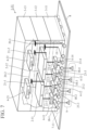
- FIG. 1 is a partially cutaway perspective cross-sectional view according to one example of a 3D structured APAA 1 of the first embodiment.
- the 3D structured APAA 1 has a configuration in which a substrate 8 having a plurality of antenna elements 9-1 and 9-2 arranged in an array, a pseudo wafer 3 that contains a group of semiconductor chips including a plurality of semiconductor chips 4-1 and 4-2 which are made of compound semiconductors, and a silicon (Si) wafer 2 made of silicon are stacked on top of each other in this order.
- the Si wafer 2 and the pseudo wafer 3 are connected to each other through a first connecting structure group 6.
- the first connecting structure group 6 includes, for example, wiring junctions between metallic wiring lines on the front surface of the Si wafer 2, solder balls, and gold bumps.
- the pseudo wafer 3 and the substrate 8 are connected to each other through a second connecting structure group 7.
- the second connecting structure group 7 includes, for example, solder balls and gold bumps.
- the solder balls and gold bumps do not need to be spherical in shape and may have other shapes.
- the solder balls and gold bumps may be, for example, cylindrical such as copper posts (copper pillars).
- An array antenna 9 is formed on the underside of the substrate 8. Examples of the array antenna 9 include a patch array antenna patterned on the substrate 8 and a waveguide slot array antenna having a 3D structure.
- the 3D structured APAA 1 has a configuration of an active phased array antenna having a 3D structure. Each element or component will be described below.
- the Si wafer 2 is a wafer made of silicon.
- the Si wafer 2 includes phase shifters, variable gain amplifiers (VGAs), and a digital control circuit (not shown) that control signals of the 3D structured APAA 1.
- Devices such as the phase shifters are provided in the Si wafer 2 located on the opposite side of the substrate 8 with the pseudo wafer 3 interposed, thereby widening the antenna plane of the substrate 8.
- the pseudo wafer 3 is a pseudo wafer in which the first compound semiconductor chip 4-1 and the second compound semiconductor chip 4-2 are covered with an insulating material.
- the pseudo wafer 3 can be formed using a technology such as fan out wafer level package (FOWLP) or a component-embedded board.
- FIG. 1 shows only two compound semiconductor chips, the pseudo wafer 3 has compound semiconductor chips (not shown) based on the number of antenna elements arranged in an array.
- Circuit elements such as transistors are formed on a surface of each of the first compound semiconductor chip 4-1 and the second compound semiconductor chip 4-2 that faces a substrate 8 side.
- the pseudo wafer 3 has a first pseudo wafer pass-through wiring line 5-1, a second pseudo wafer pass-through wiring line 5-2, and a third pseudo wafer pass-through wiring line 5-3 as wiring lines that pass through the pseudo wafer 3 in the thickness direction.
- the pseudo wafer 3 has a first via 10-1, a second via 10-2, a third via 10-3, and a fourth via 10-4 as vias that connect the compound semiconductor chips 4 in the pseudo wafer 3 to terminals provided on the front surface of the pseudo wafer 3.
- the pseudo wafer 3 has a fifth via 11-5, a sixth via 11-6, a seventh via 11-7, and an eighth via 11-8 as vias that connect the compound semiconductor chips 4 in the pseudo wafer 3 to terminals provided on the rear surface of the pseudo wafer 3.
- the first compound semiconductor chip 4-1 and the second compound semiconductor chip 4-2 are chips made of compound semiconductors such as gallium arsenide (GaAs), gallium nitride (GaN), and indium phosphide (InP).
- the first compound semiconductor chip 4-1 and the second compound semiconductor chip 4-2 each are structured to have input and output terminals for signals on both of the front surface (a surface on the substrate 8 side in FIG. 1 ) thereof and the rear surface (a surface on a Si wafer 2 side in FIG. 1 ) thereof. Input and output terminals do not need to be provided on the front and rear surfaces of all compound semiconductor chips.
- Some input and output terminals on the rear surface of the pseudo wafer 3 are connected to the input and output terminals on the rear surfaces of the first compound semiconductor chip 4-1 and the second compound semiconductor chip 4-2, and some input and output terminals on the substrate 8 side of the pseudo wafer 3 are connected to the input and output terminals on the front surfaces of the first compound semiconductor chip 4-1 and the second compound semiconductor chip 4-2.
- the first compound semiconductor chip 4-1 and the second compound semiconductor chip 4-2 are the compound semiconductor chips 4 of the same structure and have a circuit block such as that shown in FIG. 2 , for example.
- the compound semiconductor chips 4 each include a high power amplifier 12, a low noise amplifier 13, an SPDT switch 14, a transmission signal input terminal 15, a transmission and reception signal input and output terminal 16, and a reception signal output terminal 17.
- An input terminal of the high power amplifier 12 is connected to the transmission signal input terminal 15, and an output terminal of the high power amplifier 12 is connected to a first terminal of the SPDT switch 14.
- a second terminal of the SPDT switch 14 is connected to the transmission and reception signal input and output terminal 16, and a third terminal of the SPDT switch 14 is connected to an input terminal of the low noise amplifier 13.
- An output terminal of the low noise amplifier is connected to the reception signal output terminal 17 of the compound semiconductor chip 4.
- connection of wiring lines from the Si wafer 2 to the first compound semiconductor chip 4-1 and the second compound semiconductor chip 4-2 will be described.
- Power to and control signals for the Si wafer 2 are supplied from the substrate 8 through the first pseudo wafer pass-through wiring line 5-1, the second pseudo wafer pass-through wiring line 5-2, and the third pseudo wafer pass-through wiring line 5-3.
- the pseudo wafer pass-through wiring lines 5-1 to 5-3 pass through the pseudo wafer 3 in the thickness direction. Which one of the pseudo wafer pass-through wiring lines supplies power or a signal is determined as appropriate.
- the first pseudo wafer pass-through wiring line 5-1 supplies power
- the second pseudo wafer pass-through wiring line 5-2 and the third pseudo wafer pass-through wiring line 5-3 supply signals.
- Power to the first compound semiconductor chip 4-1 is supplied from the substrate 8 through the first via 10-1.
- power to the second compound semiconductor chip 4-2 is supplied from the substrate 8 through the third via 10-3.
- power to the Si wafer 2 and power to the compound semiconductor chips 4 are supplied through different lines. Namely, power separation is implemented.
- FIG. 3 is a perspective view showing a configuration of a 3D structured APAA 1M which is a variant of the 3D structured APAA 1.
- the input and output terminals of the first compound semiconductor chip 4-1 and the second compound semiconductor chip 4-2 contained in the pseudo wafer 3 are provided on both of the front and rear surfaces of the first compound semiconductor chip 4-1 and the second compound semiconductor chip 4-2, but as with the 3D structure APAA 1M of FIG. 3 , the input and output terminals of each compound semiconductor chip 4 may be provided only on the front surface (a substrate 8 side of FIG.
- the input and output terminals provided on the front surface of the compound semiconductor chip 4 (4-1M, 4-2M) are connected to terminals provided on the rear surface (a surface on an Si wafer 2 side in FIG. 3 ) of a pseudo wafer 3M, using multilayer redistribution implemented by redistribution using the FOWLP technology and a via structure (vias 11-5M to 11-8M).
- thermal vias 10-5 and 10-6 that thermally connect a surface of the pseudo wafer 3 facing the substrate 8 to the compound semiconductor chips 4 (4-1, 4-2) may be provided in the pseudo wafer 3.
- the thermal vias 10-5 and 10-6 do not electrically connect the surface of the pseudo wafer 3 facing the substrate 8 to the compound semiconductor chips 4 (4-1, 4-2).
- the thermal vias 10-5 and 10-6 are vias for heat dissipation and are made of a material with excellent thermal conductivity such as copper.
- the thermal vias 10-5 and 10-6 can be formed using the FOWLP technology.
- the high power amplifiers 12 included in the first compound semiconductor chip 4-1 and the second compound semiconductor chip 4-2 have high power consumption.
- the array antenna 9 is an array antenna in which antenna elements are arranged in an array or at regular intervals.
- Examples of the array antenna 9 include a patch array antenna patterned on the substrate 8 and a waveguide slot array antenna having a 3D structure.
- FIG. 5 is a diagram showing an example of a case in which the array antenna 9 is formed of a plurality of patch antennas, and showing a relationship between the areas of the Si wafer 2, the compound semiconductor chips 4-1 and 4-2, and the antenna elements 9-1, 9-2 as viewed from the front (radiation direction) of the array antenna 9.
- the area of the Si wafer 2 is greater than or equal to the sum of the areas of antenna planes of two adjacent elements (9-1, 9-2) among the plurality of antenna elements, and the area of each of the compound semiconductor chips 4-1 and 4-2 is smaller than the area of an antenna plane of a corresponding one of the antenna elements 9-1 and 9-2 among the plurality of antenna elements.
- transmission signals of the APAA 1 generated by the Si wafer 2 are inputted to the first compound semiconductor chip 4-1 and the second compound semiconductor chip 4-2 through the fifth via 11-5 and the seventh via 11-7.
- the transmission signal inputted to the first compound semiconductor chip 4-1 is inputted to the array antenna 9 formed on the substrate 8 through the high power amplifier 12 and the SPDT switch 14 that are contained in the first compound semiconductor chip 4-1, and the second via 10-2.
- the transmission signal inputted to the second compound semiconductor chip 4-2 is inputted to the array antenna 9 formed on the substrate 8 through the high power amplifier 12 and the SPDT switch 14 that are contained in the second compound semiconductor chip 4-2, and the fourth via 10-4.
- reception signals received by the array antenna 9 are inputted to the respective first compound semiconductor chip 4-1 and second compound semiconductor chip 4-2 through the second via 10-2 and the fourth via 10-4.
- the reception signal inputted to the first compound semiconductor chip 4-1 is amplified by the low noise amplifier 13 contained in the first compound semiconductor chip 4-1, and is inputted to the Si wafer 2 through the sixth via 11-6.
- the reception signal inputted to the second compound semiconductor chip 4-2 is amplified by the low noise amplifier 13 contained in the second compound semiconductor chip 4-2, and is inputted to the Si wafer 2 through the eighth via 11-8.
- a phase difference, amplitudes, etc., of the received signals are processed by a reception circuit contained in the Si wafer 2.
- Heat generated in the high power amplifiers 12 in the first compound semiconductor chip 4-1 and the second compound semiconductor chip 4-2 is dissipated to the substrate 8 through the thermal vias 10-5 and 10-6 as shown by an arrow 100 of FIG. 4 .
- vias 10-1M to 10-4M are also in contact with the first compound semiconductor chip 4-1 or the second compound semiconductor chip 4-2 and the substrate 8, and thus, heat generated in the high power amplifiers 12 is dissipated to the substrate 8 also through the vias 10-1M to 10-4M as shown by the arrow 100.
- the 3D structured APAA 1 includes the vias 10-1 and 10-3 for supplying power to the first compound semiconductor chip 4-1 and the second compound semiconductor chip 4-2 from the substrate 8; and the pseudo wafer pass-through wiring lines 5-1 to 5-3 for supplying power to the Si wafer 2 from the substrate 8. Namely, power to the compound semiconductor chips 4-1 and 4-2 is separated from power to the Si wafer 2. This prevents the heat generated in the compound semiconductor chips 4-1 and 4-2 from affecting the power to the Si wafer 2, and thus the operations of the 3D structured APAA 1 can be more stabilized.
- the area of the Si wafer 2 is greater than or equal to the sum of the areas of antenna planes of two adjacent elements among the plurality of antenna elements, and the area of one compound semiconductor chip among a plurality of compound semiconductor chips is smaller than the area of an antenna plane of one antenna element, and thus, it is easier to provide a feeder through which power is supplied to the Si wafer 2 from the substrate 8 separately from feeders through which power is supplied to the compound semiconductor chips 4-1 and 4-2 from the substrate 8.
- either one of the wafers may include a plurality of layers.
- a structure may be adopted in which a plurality of pseudo wafers 3-1 and 3-2 are stacked on top of each other.
- a 3D structured APAA 1MM of FIG. 6A includes the plurality of pseudo wafers 3-1 and 3-2 arranged between the Si wafer 2 and the substrate 8 having antenna elements.
- the pseudo wafer 3-1 includes, for example, compound semiconductor chips for transmission 4-3 and 4-4 which are made of GaN, etc.
- the pseudo wafer 3-2 includes, for example, compound semiconductor chips for reception 4-5 and 4-6 which are made of GaAs, etc.
- the Si wafer 2 includes an analog circuit including VGAs, phase shifters, etc., for radio-frequency signal control.
- the pseudo wafer 3 is a pseudo wafer including the compound semiconductors 4-1 and 4-2.
- the silicon wafer 2-1 includes, for example, an analog circuit including VGAs, phase shifters, etc., for radio-frequency signal control.
- the silicon wafer 2-2 includes, for example, a digital circuit for controlling the silicon wafer 2-1.
- both of the pseudo wafer and the silicon wafer may include a plurality of layers. Note that for easy understanding, in FIGS. 6A and 6B , depiction of wiring lines and bumps is omitted.
- 3D structured active phased array antenna of a second embodiment will be described.
- the same elements or components as those included in the 3D structured APAA 1 of the first embodiment are given the same numbers and an overlapping description is omitted.
- FIG. 7 is a diagram showing a 3D structured APAA 1-11 according to the second embodiment.
- the 3D structured APAA 1-11 shown in FIG. 7 includes a first pseudo wafer 3-11, a second pseudo wafer 3-12, a third pseudo wafer 3-13, a connecting structure group 7-11, a substrate 8, and an array antenna 9.
- the first pseudo wafer 3-11 includes a first GaAs chip 4-11, a second GaAs chip 4-12, a third GaAs chip 4-13, and a fourth GaAs chip 4-14.
- the first GaAs chip 4-11, the second GaAs chip 4-12, the third GaAs chip 4-13, and the fourth GaAs chip 4-14 each include the high power amplifier 12 and the low noise amplifier 13 such as those shown in FIG. 2 .
- compound semiconductor chips such as GaN chips and InP chips may be used instead of GaAs chips.
- the second pseudo wafer 3-12 includes a first Si wafer 2-11 and a second Si wafer 2-12.
- the Si wafers are also formed as pseudo wafers, and power feeders to the third pseudo wafer 3-13 are provided in a resin layer of the second pseudo wafer 3-12.
- the area of each of the Si wafers 2-11 and 2-12 contained in the second pseudo wafer 3-12 is greater than the sum of the areas of two adjacent GaAs chips contained in the first pseudo wafer 3-11 (see FIG. 5 ).
- the first Si wafer 2-11 and the second Si wafer 2-12 each include a control circuit other than a phase shifter, a variable-gain amplifier, and a VCO in a PLL.
- the third pseudo wafer 3-13 includes a first signal source GaAs chip 4-21 and a second signal source GaAs chip 4-22.
- the first signal source GaAs chip 4-21 and the second signal source GaAs chip 4-22 each include a device such as a voltage controlled oscillator (VCO). Note that instead of GaAs chips, Si chips, GaN chips, InP chips, etc., may be used.
- VCO voltage controlled oscillator
- the pseudo wafers 3-11 to 3-13 or the silicon wafers 2-11 and 2-12 included in the pseudo wafer 3-12 may also be changed in such a manner that any of the wafers includes a plurality of layers as appropriate.
- the pseudo wafer 3-11 may be changed in such a manner that the pseudo wafer 3-11 includes, as shown in FIG. 6A , a pseudo wafer having compound semiconductors for transmission and a pseudo wafer having compound semiconductors for reception by providing a plurality of layers in the pseudo wafer 3-11.
- Power to the first GaAs chip 4-11, the second GaAs chip 4-12, the third GaAs chip 4-13, and the fourth GaAs chip 4-14 included in the first pseudo wafer 3-11 is supplied through respective power wiring lines 18-1, 18-2, 18-3, and 18-4.
- the power wiring lines 18-1, 18-2, 18-3, and 18-4 electrically connect the substrate 8 to the GaAs chips 4-11 to 4-14.
- Power to the first Si wafer 2-11 and the second Si wafer 2-12 included in the second pseudo wafer 3-12 is supplied from the substrate 8 through a power wiring line 19 passing through the first pseudo wafer 3-11.
- Power to the first signal source GaAs chip 4-21 and the second signal source GaAs chip 4-22 included in the third pseudo wafer 3-13 is supplied from the substrate 8 through a power wiring line 20-1 passing through the first pseudo wafer 3-11 and the second pseudo wafer 3-12, and a power wiring line 20-2 in the third pseudo wafer 3-13.
- a radio-frequency signal between the first signal source GaAs chip 4-21 and the first Si wafer 2-11 is supplied through a radio-frequency wiring line 21-1 that connects these elements, and a radio-frequency signal between the second signal source GaAs chip 4-22 and the second Si wafer 2-12 is supplied through a radio-frequency wiring line 21-2 that connects these elements.
- a radio-frequency signal between the first Si wafer 2-11 and the first GaAs chip 4-11 is supplied through a radio-frequency wiring line 22-1 that connects these elements, and a radio-frequency signal between the first Si wafer 2-11 and the second GaAs chip 4-12 is supplied through a radio-frequency wiring line 22-2 that connects these elements.
- a radio-frequency signal between the second Si wafer 2-12 and the third GaAs chip 4-13 is supplied through a radio-frequency wiring line 22-3 that connects these elements, and a radio-frequency signal between the second Si wafer 2-12 and the fourth GaAs chip 4-14 is supplied through a radio-frequency wiring line 22-4 that connects these elements.
- the input and output terminals of each of the GaAs chips 4-11 to 4-14 are provided on both of the front and rear surfaces of the chip, as shown in the variant of the first embodiment ( FIG. 3 ), the input and output terminals may be arranged only on one surface (front surface) of each chip, and multilayer redistribution may be provided using the FOWLP technology.
- the radio-frequency wiring lines 22-1 to 22-4 are routed to the front surfaces of the GaAs chips 4-11 to 4-14 (surfaces of the GaAs chips 4-11 to 4-14 facing antenna elements).
- thermal vias 23-1 to 23-4 that thermally connect a surface of the first pseudo wafer 3-11 facing the substrate 8 to the GaAs chips 4-11 to 4-14.
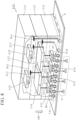
- FIG. 8 shows heat dissipation paths of the 3D structured APAA 1-11 shown in FIG. 7 .
- the power consumption of the first GaAs chip 4-11, the second GaAs chip 4-12, the third GaAs chip 4-13, and the fourth GaAs chip 4-14 each including the high power amplifier 12 is high.
- heat generated in the 3D structured APAA 1-11 is dissipated to the substrate 8 through the thermal vias 23-1 to 23-4.
- such heat is dissipated to the substrate 8 also through wiring lines between the GaAs chips 4-11 to 4-14 and a surface of the first pseudo wafer 3-11 facing the substrate 8 (e.g., the power wiring line 18-1 and wiring lines between the GaAs chips 4 and the antenna elements) as shown by the arrow 100.
- the 3D structured APAA 1-11 configured in the above-described manner operates in the same manner as the 3D structured APAA 1 according to the first embodiment.
- the 3D structured APAA 1-11 includes the power wiring lines 18-1 to 18-4 for supplying power to the GaAs chips 4-11 to 4-14 from the substrate 8; the power wiring line 19 for supplying power to the Si wafers 2-11 and 2-12 from the substrate 8, the power wiring line 19 passing through the first pseudo wafer 3-11 in the thickness direction; and the power wiring line 20-1 for supplying power to the signal source GaAs chips 4-21 and 4-22 from the substrate 8, the power wiring line 20-1 passing through the second pseudo wafer 3-12 in the thickness direction.
- power to the GaAs chips 4-11 to 4-14, power to the Si wafers 2-11 and 2-12, and power to the signal source GaAs chips 4-21 and 4-22 are separated from each other.
- power to the first Si wafer 2-11 and the second Si wafer 2-12 contained in the second pseudo wafer 3-12 is fed without passing through the GaAs chips 4-11 to 4-14 contained in the first pseudo wafer 3-11.
- power to the first signal source GaAs chip 4-21 and the second signal source GaAs chip 4-22 contained in the third pseudo wafer 3-13 is fed without passing through the first GaAs chips 4-11 to 4-14 contained in the first pseudo wafer 3-11 or the first Si wafer 2-11 or the second Si wafer 2-12 contained in the second pseudo wafer 3-12. Therefore, power used by the signal source GaAs chips 4-21 and 4-22 does not pass through the Si wafers 2-11 and 2-12.
- An active phased array antenna (1; 1M) is an active phased array antenna (1; 1M) including a substrate (8) having a plurality of antenna elements (9-1, 9-2); a pseudo wafer (3; 3M) containing a group of semiconductor chips including a plurality of semiconductor chips (4-1, 4-2; 4-1M, 4-2M) made of compound semiconductors; and a silicon wafer (2; 2-11, 2-12) made of silicon, the substrate, the pseudo wafer, and the silicon wafer being stacked on top of each other in this order, and the pseudo wafer includes first feeders (10-1, 10-3; 10-1M, 10-3M) for supplying power to the group of semiconductor chips from the substrate; and a second feeder (5-1 to 5-3; 5-1M to 5-3M) for supplying power to the silicon wafer from the substrate, the second feeder passing through the pseudo wafer in a thickness direction of the pseudo wafer.
- An active phased array antenna of additional note 2 is the active phased array antenna of additional note 1, and the area of the silicon wafer is greater than or equal to the sum of the areas of antenna planes of two adjacent elements among the plurality of antenna elements, and the area of one semiconductor chip among the plurality of semiconductor chips is smaller than the area of an antenna plane of one antenna element among the plurality of antenna elements.
- An active phased array antenna of additional note 3 is the active phased array antenna described in additional note 1 or 2, and the plurality of semiconductor chips includes a semiconductor chip having input and output terminals (15 to 17) formed on both the front and rear surfaces of the semiconductor chip.
- An active phased array antenna of additional note 4 is the active phased array antenna described in additional note 1 or 2, and the plurality of semiconductor chips includes a semiconductor chip having input and output terminals formed only on one surface of the semiconductor chip, and the pseudo wafer has multilayer redistribution (11-5M to 11-8M) that connects the input and output terminals of the semiconductor chip to input and output terminals of the silicon wafer.
- An active phased array antenna of additional note 5 is any one of the active phased array antennas described in additional notes 1 to 4, and the pseudo wafer has a thermal via (10-5, 10-6) that thermally connects, instead of electrically connects, a surface of the pseudo wafer facing the substrate to any one of the semiconductor chips included in the group of semiconductor chips.
- An active phased array antenna (1-11) is an active phased array antenna (1-11) including a substrate (8) having a plurality of antenna elements (9-1, 9-2) formed thereon; a first pseudo wafer (3-11) containing a first group of semiconductor chips including a plurality of semiconductor chips (4-11 to 4-14) made of compound semiconductors; a second pseudo wafer (3-12) containing one or more silicon wafers (2-11, 2-12) made of silicon; and a third pseudo wafer (3-13) containing a second group of semiconductor chips including a plurality of semiconductor chips (4-21, 4-22) made of compound semiconductors, the substrate, the first pseudo wafer, the second pseudo wafer, and the third pseudo wafer being stacked on top of each other in this order, and the first pseudo wafer includes first feeders (18-1 to 18-4) for supplying power to the first group of semiconductor chips from the substrate; a second feeder (19) for supplying power to the one or more silicon wafers from the substrate, the second feeder passing through the first pseudo wafer in a thickness direction of the first pseudo
- An active phased array antenna of additional note 7 is the active phased array antenna described in additional note 6, and the plurality of semiconductor chips includes a semiconductor chip having input and output terminals (15 to 17) formed on both the front and rear surfaces of the semiconductor chip.
- An active phased array antenna of additional note 8 is the active phased array antenna described in additional note 6, and the plurality of semiconductor chips includes a semiconductor chip having input and output terminals formed only on one surface of the semiconductor chip, and the first pseudo wafer has multilayer redistribution (11-5M to 11-8M) that connects the input and output terminals of the semiconductor chip to input and output terminals of the silicon wafer.
- An active phased array antenna of additional note 9 is any one of the active phased array antennas described in additional notes 6 to 8, and the first pseudo wafer has a thermal via (23-1 to 23-4) that thermally connects, instead of electrically connects, a surface of the first pseudo wafer facing the substrate to any one of the semiconductor chips included in the first group of semiconductor chips.
- An active phased array antenna of additional note 10 is any one of the active phased array antennas described in additional notes 6 to 9, and the third feeder passes through the second pseudo wafer in a thickness direction of the second pseudo wafer.
- an active phased array antenna of the present disclosure power to devices for allowing the active phased array antenna to operate is separated.
- the active phased array antenna of the present disclosure can be used as an active phased array antenna whose operations are more stabilized.
Landscapes
- Engineering & Computer Science (AREA)
- Microelectronics & Electronic Packaging (AREA)
- Variable-Direction Aerials And Aerial Arrays (AREA)
- Semiconductor Integrated Circuits (AREA)
Abstract
Description
- The present disclosure relates to an active phased array antenna.
- FIG. 21 of Patent Literature 1 and description of a specification related to FIG. 21 disclose an antenna having a 3D structure in which a substrate (150), a high-density, low-speed silicon IC device (151), an insulating substrate (152), a low-density, high-speed device (153), and a substrate (154) having patch antennas (159) are stacked on top of each other in this order. The high-density, low-speed silicon IC device has elements (155) and wiring lines (156). The low-density, high-speed device has heterojunction bipolar transistors formed thereon.
- Patent Literature 1:
JP 2015-84421 A - According to the antenna disclosed in this Patent Literature 1, the area of each compound semiconductor IC chip (157) arranged at a low density is larger than the area of each of the silicon IC chips (155) arranged at a high density. Hence, when power is supplied to a silicon wafer (Si wafer) from the substrate having the antennas, it is difficult to provide a feeder that directly connects the substrate having the antennas to the silicon wafer. This necessitates an area for feeding that is provided on the device having the compound semiconductor IC chips mounted thereon, which causes the compound semiconductor IC chips and the Si wafer to share power. Thus, there is a problem that there is a possibility of power supply to the Si wafer becoming unstable due to heat generated upon operation of the compound semiconductor IC chips.
- The present disclosure is made to solve a problem such as that described above, and an object of one aspect of embodiments is to provide an active phased array antenna having a 3D structure in which power to an Si wafer is separated from power to compound semiconductor chips.
- One aspect of an active phased array antenna of an embodiment is an active phased array antenna including a substrate having a plurality of antenna elements; a pseudo wafer containing a group of semiconductor chips including a plurality of semiconductor chips made of compound semiconductors; and a silicon wafer made of silicon, the substrate, the pseudo wafer, and the silicon wafer being stacked on top of each other in this order, and the pseudo wafer includes first feeders to supply power to the group of semiconductor chips from the substrate; and a second feeder to supply power to the silicon wafer from the substrate, the second feeder passing through the pseudo wafer in a thickness direction of the pseudo wafer.
- Another aspect of an active phased array antenna of an embodiment is an active phased array antenna including a substrate having a plurality of antenna elements formed thereon; a first pseudo wafer containing a first group of semiconductor chips including a plurality of semiconductor chips made of compound semiconductors; a second pseudo wafer containing one or more silicon wafers made of silicon; and a third pseudo wafer containing a second group of semiconductor chips including a plurality of semiconductor chips made of compound semiconductors, the substrate, the first pseudo wafer, the second pseudo wafer, and the third pseudo wafer being stacked on top of each other in this order, and the first pseudo wafer includes first feeders to supply power to the first group of semiconductor chips from the substrate; a second feeder to supply power to the one or more silicon wafers from the substrate, the second feeder passing through the first pseudo wafer in a thickness direction of the first pseudo wafer; and a third feeder to supply power to the second group of semiconductor chips from the substrate, the third feeder passing through the first pseudo wafer in the thickness direction of the first pseudo wafer.
- According to the above-described one aspect of the active phased array antenna, the pseudo wafer includes the first feeders for supplying power to the group of semiconductor chips from the substrate; and the second feeder for supplying power to the silicon wafer from the substrate, the second feeder passing through the pseudo wafer in the thickness direction of the pseudo wafer. Thus, power to the Si wafer is separated from power to the compound semiconductor chips.
- According to the above-described another aspect of the active phased array antenna, the first pseudo wafer includes the first feeders for supplying power to the first group of semiconductor chips from the substrate; the second feeder for supplying power to the silicon wafer from the substrate, the second feeder passing through the first pseudo wafer in the thickness direction of the first pseudo wafer; and the third feeder for supplying power to the second group of semiconductor chips from the substrate, the third feeder passing through the first pseudo wafer in the thickness direction of the first pseudo wafer. Thus, power to the compound semiconductor chips is separated from power to the Si wafer.
-
-
FIG. 1 is a partially cutaway perspective cross-sectional view according to one example of a 3D structured active phased array antenna (APAA) of a first embodiment. Note that circuit elements formed on compound semiconductor chips contained in a pseudo wafer are represented by circuit symbols. -
FIG. 2 is a block diagram of the inside of a first compound semiconductor chip and a second compound semiconductor chip ofFIG. 1 . -
FIG. 3 is a partially cutaway perspective cross-sectional view according to a variant of the 3D structured APAA ofFIG. 1 . Depiction of circuit elements included in compound semiconductor chips contained in a pseudo wafer is omitted for easy understanding. -
FIG. 4 is a diagram showing heat dissipation paths of the 3D structured APAA ofFIG. 1 . -
FIG. 5 is a diagram showing a relationship between the areas of a silicon wafer, the compound semiconductor chips, and antenna elements. -
FIG. 6A is a conceptual configuration diagram according to a variant of the 3D structured APAA ofFIG. 1 . -
FIG. 6B is a conceptual configuration diagram according to a variant of the 3D structured APAA ofFIG. 1 . -
FIG. 7 is a partially cutaway perspective cross-sectional view according to one example of a 3D structured active phased array antenna (APAA) of a second embodiment. -
FIG. 8 is a diagram showing heat dissipation paths of the 3D structured APAA ofFIG. 7 . - Embodiments of the present disclosure will be described below with reference to the accompanying drawings.
- With reference to
FIGS. 1 to 6B , a 3D structured active phased array antenna (APAA) of a first embodiment will be described. First, a configuration of the 3D structured APAA will be described. -
FIG. 1 is a partially cutaway perspective cross-sectional view according to one example of a 3D structured APAA 1 of the first embodiment. As shown inFIG. 1 , the 3D structured APAA 1 has a configuration in which asubstrate 8 having a plurality of antenna elements 9-1 and 9-2 arranged in an array, apseudo wafer 3 that contains a group of semiconductor chips including a plurality of semiconductor chips 4-1 and 4-2 which are made of compound semiconductors, and a silicon (Si)wafer 2 made of silicon are stacked on top of each other in this order. The Si wafer 2 and thepseudo wafer 3 are connected to each other through a first connectingstructure group 6. The first connectingstructure group 6 includes, for example, wiring junctions between metallic wiring lines on the front surface of theSi wafer 2, solder balls, and gold bumps. Thepseudo wafer 3 and thesubstrate 8 are connected to each other through a second connectingstructure group 7. The second connectingstructure group 7 includes, for example, solder balls and gold bumps. The solder balls and gold bumps do not need to be spherical in shape and may have other shapes. The solder balls and gold bumps may be, for example, cylindrical such as copper posts (copper pillars). Anarray antenna 9 is formed on the underside of thesubstrate 8. Examples of thearray antenna 9 include a patch array antenna patterned on thesubstrate 8 and a waveguide slot array antenna having a 3D structure. For one antenna element, one phase shifter is included in theSi wafer 2, and ahigh power amplifier 12 and alow noise amplifier 13 are included in thepseudo wafer 3. As such, the 3D structured APAA 1 has a configuration of an active phased array antenna having a 3D structure. Each element or component will be described below. - The Si wafer 2 is a wafer made of silicon. The
Si wafer 2 includes phase shifters, variable gain amplifiers (VGAs), and a digital control circuit (not shown) that control signals of the 3D structured APAA 1. Devices such as the phase shifters are provided in theSi wafer 2 located on the opposite side of thesubstrate 8 with thepseudo wafer 3 interposed, thereby widening the antenna plane of thesubstrate 8. - The
pseudo wafer 3 is a pseudo wafer in which the first compound semiconductor chip 4-1 and the second compound semiconductor chip 4-2 are covered with an insulating material. Thepseudo wafer 3 can be formed using a technology such as fan out wafer level package (FOWLP) or a component-embedded board. AlthoughFIG. 1 shows only two compound semiconductor chips, thepseudo wafer 3 has compound semiconductor chips (not shown) based on the number of antenna elements arranged in an array. - Circuit elements such as transistors are formed on a surface of each of the first compound semiconductor chip 4-1 and the second compound semiconductor chip 4-2 that faces a
substrate 8 side. - The
pseudo wafer 3 has a first pseudo wafer pass-through wiring line 5-1, a second pseudo wafer pass-through wiring line 5-2, and a third pseudo wafer pass-through wiring line 5-3 as wiring lines that pass through thepseudo wafer 3 in the thickness direction. In addition, thepseudo wafer 3 has a first via 10-1, a second via 10-2, a third via 10-3, and a fourth via 10-4 as vias that connect the compound semiconductor chips 4 in thepseudo wafer 3 to terminals provided on the front surface of thepseudo wafer 3. In addition, thepseudo wafer 3 has a fifth via 11-5, a sixth via 11-6, a seventh via 11-7, and an eighth via 11-8 as vias that connect the compound semiconductor chips 4 in thepseudo wafer 3 to terminals provided on the rear surface of thepseudo wafer 3. - The first compound semiconductor chip 4-1 and the second compound semiconductor chip 4-2 are chips made of compound semiconductors such as gallium arsenide (GaAs), gallium nitride (GaN), and indium phosphide (InP). The first compound semiconductor chip 4-1 and the second compound semiconductor chip 4-2 each are structured to have input and output terminals for signals on both of the front surface (a surface on the
substrate 8 side inFIG. 1 ) thereof and the rear surface (a surface on aSi wafer 2 side inFIG. 1 ) thereof. Input and output terminals do not need to be provided on the front and rear surfaces of all compound semiconductor chips. Some input and output terminals on the rear surface of thepseudo wafer 3 are connected to the input and output terminals on the rear surfaces of the first compound semiconductor chip 4-1 and the second compound semiconductor chip 4-2, and some input and output terminals on thesubstrate 8 side of thepseudo wafer 3 are connected to the input and output terminals on the front surfaces of the first compound semiconductor chip 4-1 and the second compound semiconductor chip 4-2. - The first compound semiconductor chip 4-1 and the second compound semiconductor chip 4-2 are the compound semiconductor chips 4 of the same structure and have a circuit block such as that shown in
FIG. 2 , for example. As shown inFIG. 2 , the compound semiconductor chips 4 each include ahigh power amplifier 12, alow noise amplifier 13, anSPDT switch 14, a transmissionsignal input terminal 15, a transmission and reception signal input andoutput terminal 16, and a receptionsignal output terminal 17. An input terminal of thehigh power amplifier 12 is connected to the transmissionsignal input terminal 15, and an output terminal of thehigh power amplifier 12 is connected to a first terminal of theSPDT switch 14. A second terminal of theSPDT switch 14 is connected to the transmission and reception signal input andoutput terminal 16, and a third terminal of theSPDT switch 14 is connected to an input terminal of thelow noise amplifier 13. An output terminal of the low noise amplifier is connected to the receptionsignal output terminal 17 of the compound semiconductor chip 4. - Connection of wiring lines from the
Si wafer 2 to the first compound semiconductor chip 4-1 and the second compound semiconductor chip 4-2 will be described. Power to and control signals for theSi wafer 2 are supplied from thesubstrate 8 through the first pseudo wafer pass-through wiring line 5-1, the second pseudo wafer pass-through wiring line 5-2, and the third pseudo wafer pass-through wiring line 5-3. As shown inFIG. 1 , the pseudo wafer pass-through wiring lines 5-1 to 5-3 pass through thepseudo wafer 3 in the thickness direction. Which one of the pseudo wafer pass-through wiring lines supplies power or a signal is determined as appropriate. For example, the first pseudo wafer pass-through wiring line 5-1 supplies power, and the second pseudo wafer pass-through wiring line 5-2 and the third pseudo wafer pass-through wiring line 5-3 supply signals. Power to the first compound semiconductor chip 4-1 is supplied from thesubstrate 8 through the first via 10-1. Likewise, power to the second compound semiconductor chip 4-2 is supplied from thesubstrate 8 through the third via 10-3. As such, power to theSi wafer 2 and power to the compound semiconductor chips 4 are supplied through different lines. Namely, power separation is implemented. - Wiring lines to the first compound semiconductor chip 4-1 and the second compound semiconductor chip 4-2 may be changed as shown in
FIG. 3. FIG. 3 is a perspective view showing a configuration of a 3D structured APAA 1M which is a variant of the 3D structured APAA 1. In the 3D structured APAA 1 ofFIG. 1 , the input and output terminals of the first compound semiconductor chip 4-1 and the second compound semiconductor chip 4-2 contained in thepseudo wafer 3 are provided on both of the front and rear surfaces of the first compound semiconductor chip 4-1 and the second compound semiconductor chip 4-2, but as with the 3D structure APAA 1M ofFIG. 3 , the input and output terminals of each compound semiconductor chip 4 may be provided only on the front surface (asubstrate 8 side ofFIG. 3 ) of the compound semiconductor chip 4 (4-1M, 4-2M). In this case, the input and output terminals provided on the front surface of the compound semiconductor chip 4 (4-1M, 4-2M) are connected to terminals provided on the rear surface (a surface on anSi wafer 2 side inFIG. 3 ) of apseudo wafer 3M, using multilayer redistribution implemented by redistribution using the FOWLP technology and a via structure (vias 11-5M to 11-8M). - In addition, thermal vias 10-5 and 10-6 that thermally connect a surface of the
pseudo wafer 3 facing thesubstrate 8 to the compound semiconductor chips 4 (4-1, 4-2) may be provided in thepseudo wafer 3. The thermal vias 10-5 and 10-6 do not electrically connect the surface of thepseudo wafer 3 facing thesubstrate 8 to the compound semiconductor chips 4 (4-1, 4-2). The thermal vias 10-5 and 10-6 are vias for heat dissipation and are made of a material with excellent thermal conductivity such as copper. The thermal vias 10-5 and 10-6 can be formed using the FOWLP technology. Thehigh power amplifiers 12 included in the first compound semiconductor chip 4-1 and the second compound semiconductor chip 4-2 have high power consumption. By providing the thermal vias 10-5 and 10-6, heat generated in the first compound semiconductor chip 4-1 and the second compound semiconductor chip 4-2 can be dissipated to thesubstrate 8 serving as a heat dissipator. - The
array antenna 9 is an array antenna in which antenna elements are arranged in an array or at regular intervals. Examples of thearray antenna 9 include a patch array antenna patterned on thesubstrate 8 and a waveguide slot array antenna having a 3D structure. Here, with reference toFIG. 5 , a relationship between the areas of theSi wafer 2, the compound semiconductor chips 4-1 and 4-2, and the antenna elements 9-1, 9-2 will be described.FIG. 5 is a diagram showing an example of a case in which thearray antenna 9 is formed of a plurality of patch antennas, and showing a relationship between the areas of theSi wafer 2, the compound semiconductor chips 4-1 and 4-2, and the antenna elements 9-1, 9-2 as viewed from the front (radiation direction) of thearray antenna 9. - As shown in
FIG. 5 , the area of theSi wafer 2 is greater than or equal to the sum of the areas of antenna planes of two adjacent elements (9-1, 9-2) among the plurality of antenna elements, and the area of each of the compound semiconductor chips 4-1 and 4-2 is smaller than the area of an antenna plane of a corresponding one of the antenna elements 9-1 and 9-2 among the plurality of antenna elements. By having such a relationship, it is easier to provide a feeder through which power is supplied to theSi wafer 2 from thesubstrate 8 separately from feeders through which power is supplied to the compound semiconductor chips 4-1 and 4-2 from thesubstrate 8. - Next, transmission and reception operations of the 3D structured APAA 1 will be described. Upon transmission, transmission signals of the APAA 1 generated by the
Si wafer 2 are inputted to the first compound semiconductor chip 4-1 and the second compound semiconductor chip 4-2 through the fifth via 11-5 and the seventh via 11-7. The transmission signal inputted to the first compound semiconductor chip 4-1 is inputted to thearray antenna 9 formed on thesubstrate 8 through thehigh power amplifier 12 and theSPDT switch 14 that are contained in the first compound semiconductor chip 4-1, and the second via 10-2. On the other hand, the transmission signal inputted to the second compound semiconductor chip 4-2 is inputted to thearray antenna 9 formed on thesubstrate 8 through thehigh power amplifier 12 and theSPDT switch 14 that are contained in the second compound semiconductor chip 4-2, and the fourth via 10-4. - Upon reception, reception signals received by the
array antenna 9 are inputted to the respective first compound semiconductor chip 4-1 and second compound semiconductor chip 4-2 through the second via 10-2 and the fourth via 10-4. The reception signal inputted to the first compound semiconductor chip 4-1 is amplified by thelow noise amplifier 13 contained in the first compound semiconductor chip 4-1, and is inputted to theSi wafer 2 through the sixth via 11-6. On the other hand, the reception signal inputted to the second compound semiconductor chip 4-2 is amplified by thelow noise amplifier 13 contained in the second compound semiconductor chip 4-2, and is inputted to theSi wafer 2 through the eighth via 11-8. In theSi wafer 2, a phase difference, amplitudes, etc., of the received signals are processed by a reception circuit contained in theSi wafer 2. - Heat generated in the
high power amplifiers 12 in the first compound semiconductor chip 4-1 and the second compound semiconductor chip 4-2 is dissipated to thesubstrate 8 through the thermal vias 10-5 and 10-6 as shown by anarrow 100 ofFIG. 4 . In addition, vias 10-1M to 10-4M are also in contact with the first compound semiconductor chip 4-1 or the second compound semiconductor chip 4-2 and thesubstrate 8, and thus, heat generated in thehigh power amplifiers 12 is dissipated to thesubstrate 8 also through the vias 10-1M to 10-4M as shown by thearrow 100. - As described above, the 3D structured APAA 1 includes the vias 10-1 and 10-3 for supplying power to the first compound semiconductor chip 4-1 and the second compound semiconductor chip 4-2 from the
substrate 8; and the pseudo wafer pass-through wiring lines 5-1 to 5-3 for supplying power to theSi wafer 2 from thesubstrate 8. Namely, power to the compound semiconductor chips 4-1 and 4-2 is separated from power to theSi wafer 2. This prevents the heat generated in the compound semiconductor chips 4-1 and 4-2 from affecting the power to theSi wafer 2, and thus the operations of the 3D structured APAA 1 can be more stabilized. - In addition, the area of the
Si wafer 2 is greater than or equal to the sum of the areas of antenna planes of two adjacent elements among the plurality of antenna elements, and the area of one compound semiconductor chip among a plurality of compound semiconductor chips is smaller than the area of an antenna plane of one antenna element, and thus, it is easier to provide a feeder through which power is supplied to theSi wafer 2 from thesubstrate 8 separately from feeders through which power is supplied to the compound semiconductor chips 4-1 and 4-2 from thesubstrate 8. - Although the first embodiment and the variant thereof show a case in which the pseudo wafer and the silicon wafer each have one layer, either one of the wafers may include a plurality of layers. For example, as shown in
FIG. 6A , a structure may be adopted in which a plurality of pseudo wafers 3-1 and 3-2 are stacked on top of each other. A 3D structured APAA 1MM ofFIG. 6A includes the plurality of pseudo wafers 3-1 and 3-2 arranged between theSi wafer 2 and thesubstrate 8 having antenna elements. The pseudo wafer 3-1 includes, for example, compound semiconductor chips for transmission 4-3 and 4-4 which are made of GaN, etc., and the pseudo wafer 3-2 includes, for example, compound semiconductor chips for reception 4-5 and 4-6 which are made of GaAs, etc. As in the first embodiment, theSi wafer 2 includes an analog circuit including VGAs, phase shifters, etc., for radio-frequency signal control. - Alternatively, as shown in
FIG. 6B , a structure may be adopted in which a plurality of silicon wafers 2-1 and 2-2 are stacked on top of each other. In a 3D structured APAA 1MMM ofFIG. 6B , as in the first embodiment, thepseudo wafer 3 is a pseudo wafer including the compound semiconductors 4-1 and 4-2. The silicon wafer 2-1 includes, for example, an analog circuit including VGAs, phase shifters, etc., for radio-frequency signal control. The silicon wafer 2-2 includes, for example, a digital circuit for controlling the silicon wafer 2-1. - As a still another variant, by combining together a configuration of
FIG. 6A and a configuration ofFIG. 6B , both of the pseudo wafer and the silicon wafer may include a plurality of layers. Note that for easy understanding, inFIGS. 6A and 6B , depiction of wiring lines and bumps is omitted. - Next, with reference to
FIGS. 2 ,3 , and5 to 8 , a 3D structured active phased array antenna of a second embodiment will be described. The same elements or components as those included in the 3D structured APAA 1 of the first embodiment are given the same numbers and an overlapping description is omitted. -
FIG. 7 is a diagram showing a 3D structured APAA 1-11 according to the second embodiment. The 3D structured APAA 1-11 shown inFIG. 7 includes a first pseudo wafer 3-11, a second pseudo wafer 3-12, a third pseudo wafer 3-13, a connecting structure group 7-11, asubstrate 8, and anarray antenna 9. - The first pseudo wafer 3-11 includes a first GaAs chip 4-11, a second GaAs chip 4-12, a third GaAs chip 4-13, and a fourth GaAs chip 4-14. The first GaAs chip 4-11, the second GaAs chip 4-12, the third GaAs chip 4-13, and the fourth GaAs chip 4-14 each include the
high power amplifier 12 and thelow noise amplifier 13 such as those shown inFIG. 2 . Note that instead of GaAs chips, compound semiconductor chips such as GaN chips and InP chips may be used. - The second pseudo wafer 3-12 includes a first Si wafer 2-11 and a second Si wafer 2-12. In the second embodiment, the Si wafers are also formed as pseudo wafers, and power feeders to the third pseudo wafer 3-13 are provided in a resin layer of the second pseudo wafer 3-12. As in the first embodiment, the area of each of the Si wafers 2-11 and 2-12 contained in the second pseudo wafer 3-12 is greater than the sum of the areas of two adjacent GaAs chips contained in the first pseudo wafer 3-11 (see
FIG. 5 ). The first Si wafer 2-11 and the second Si wafer 2-12 each include a control circuit other than a phase shifter, a variable-gain amplifier, and a VCO in a PLL. - The third pseudo wafer 3-13 includes a first signal source GaAs chip 4-21 and a second signal source GaAs chip 4-22. The first signal source GaAs chip 4-21 and the second signal source GaAs chip 4-22 each include a device such as a voltage controlled oscillator (VCO). Note that instead of GaAs chips, Si chips, GaN chips, InP chips, etc., may be used.
- In addition, as described with reference to
FIGS. 6A and 6B , the pseudo wafers 3-11 to 3-13 or the silicon wafers 2-11 and 2-12 included in the pseudo wafer 3-12 may also be changed in such a manner that any of the wafers includes a plurality of layers as appropriate. For example, the pseudo wafer 3-11 may be changed in such a manner that the pseudo wafer 3-11 includes, as shown inFIG. 6A , a pseudo wafer having compound semiconductors for transmission and a pseudo wafer having compound semiconductors for reception by providing a plurality of layers in the pseudo wafer 3-11. - Wiring lines between the
substrate 8, the first pseudo wafer 3-11, the second pseudo wafer 3-12, and the third pseudo wafer 3-13 will be described. - Power to the first GaAs chip 4-11, the second GaAs chip 4-12, the third GaAs chip 4-13, and the fourth GaAs chip 4-14 included in the first pseudo wafer 3-11 is supplied through respective power wiring lines 18-1, 18-2, 18-3, and 18-4. The power wiring lines 18-1, 18-2, 18-3, and 18-4 electrically connect the
substrate 8 to the GaAs chips 4-11 to 4-14. - Power to the first Si wafer 2-11 and the second Si wafer 2-12 included in the second pseudo wafer 3-12 is supplied from the
substrate 8 through apower wiring line 19 passing through the first pseudo wafer 3-11. - Power to the first signal source GaAs chip 4-21 and the second signal source GaAs chip 4-22 included in the third pseudo wafer 3-13 is supplied from the
substrate 8 through a power wiring line 20-1 passing through the first pseudo wafer 3-11 and the second pseudo wafer 3-12, and a power wiring line 20-2 in the third pseudo wafer 3-13. - A radio-frequency signal between the first signal source GaAs chip 4-21 and the first Si wafer 2-11 is supplied through a radio-frequency wiring line 21-1 that connects these elements, and a radio-frequency signal between the second signal source GaAs chip 4-22 and the second Si wafer 2-12 is supplied through a radio-frequency wiring line 21-2 that connects these elements.
- A radio-frequency signal between the first Si wafer 2-11 and the first GaAs chip 4-11 is supplied through a radio-frequency wiring line 22-1 that connects these elements, and a radio-frequency signal between the first Si wafer 2-11 and the second GaAs chip 4-12 is supplied through a radio-frequency wiring line 22-2 that connects these elements. In addition, a radio-frequency signal between the second Si wafer 2-12 and the third GaAs chip 4-13 is supplied through a radio-frequency wiring line 22-3 that connects these elements, and a radio-frequency signal between the second Si wafer 2-12 and the fourth GaAs chip 4-14 is supplied through a radio-frequency wiring line 22-4 that connects these elements.
- Although in
FIG. 7 the input and output terminals of each of the GaAs chips 4-11 to 4-14 are provided on both of the front and rear surfaces of the chip, as shown in the variant of the first embodiment (FIG. 3 ), the input and output terminals may be arranged only on one surface (front surface) of each chip, and multilayer redistribution may be provided using the FOWLP technology. In this case, the radio-frequency wiring lines 22-1 to 22-4 are routed to the front surfaces of the GaAs chips 4-11 to 4-14 (surfaces of the GaAs chips 4-11 to 4-14 facing antenna elements). - In addition, as in the case of the first embodiment, in the first pseudo wafer 3-11 there may be provided thermal vias 23-1 to 23-4 that thermally connect a surface of the first pseudo wafer 3-11 facing the
substrate 8 to the GaAs chips 4-11 to 4-14. -
FIG. 8 shows heat dissipation paths of the 3D structured APAA 1-11 shown inFIG. 7 . The power consumption of the first GaAs chip 4-11, the second GaAs chip 4-12, the third GaAs chip 4-13, and the fourth GaAs chip 4-14 each including thehigh power amplifier 12 is high. As in the first embodiment, as shown byarrow 100, heat generated in the 3D structured APAA 1-11 is dissipated to thesubstrate 8 through the thermal vias 23-1 to 23-4. In addition, as in the first embodiment, such heat is dissipated to thesubstrate 8 also through wiring lines between the GaAs chips 4-11 to 4-14 and a surface of the first pseudo wafer 3-11 facing the substrate 8 (e.g., the power wiring line 18-1 and wiring lines between the GaAs chips 4 and the antenna elements) as shown by thearrow 100. - The 3D structured APAA 1-11 configured in the above-described manner operates in the same manner as the 3D structured APAA 1 according to the first embodiment.
- As described above, the 3D structured APAA 1-11 includes the power wiring lines 18-1 to 18-4 for supplying power to the GaAs chips 4-11 to 4-14 from the
substrate 8; thepower wiring line 19 for supplying power to the Si wafers 2-11 and 2-12 from thesubstrate 8, thepower wiring line 19 passing through the first pseudo wafer 3-11 in the thickness direction; and the power wiring line 20-1 for supplying power to the signal source GaAs chips 4-21 and 4-22 from thesubstrate 8, the power wiring line 20-1 passing through the second pseudo wafer 3-12 in the thickness direction. Namely, power to the GaAs chips 4-11 to 4-14, power to the Si wafers 2-11 and 2-12, and power to the signal source GaAs chips 4-21 and 4-22 are separated from each other. - Hence, power to the first Si wafer 2-11 and the second Si wafer 2-12 contained in the second pseudo wafer 3-12 is fed without passing through the GaAs chips 4-11 to 4-14 contained in the first pseudo wafer 3-11. Likewise, power to the first signal source GaAs chip 4-21 and the second signal source GaAs chip 4-22 contained in the third pseudo wafer 3-13 is fed without passing through the first GaAs chips 4-11 to 4-14 contained in the first pseudo wafer 3-11 or the first Si wafer 2-11 or the second Si wafer 2-12 contained in the second pseudo wafer 3-12. Therefore, power used by the signal source GaAs chips 4-21 and 4-22 does not pass through the Si wafers 2-11 and 2-12. This prevents the heat generated in the GaAs chips 4-11 to 4-14 from affecting the power to the Si wafers 2-11 and 2-12 and the power to the signal source GaAs chips 4-21 and 4-22, and thus, the operations of the 3D structured APAA 1-11 can be more stabilized.
- Some aspects of the embodiments of the present disclosure will be summarized below.
- An active phased array antenna (1; 1M) is an active phased array antenna (1; 1M) including a substrate (8) having a plurality of antenna elements (9-1, 9-2); a pseudo wafer (3; 3M) containing a group of semiconductor chips including a plurality of semiconductor chips (4-1, 4-2; 4-1M, 4-2M) made of compound semiconductors; and a silicon wafer (2; 2-11, 2-12) made of silicon, the substrate, the pseudo wafer, and the silicon wafer being stacked on top of each other in this order, and the pseudo wafer includes first feeders (10-1, 10-3; 10-1M, 10-3M) for supplying power to the group of semiconductor chips from the substrate; and a second feeder (5-1 to 5-3; 5-1M to 5-3M) for supplying power to the silicon wafer from the substrate, the second feeder passing through the pseudo wafer in a thickness direction of the pseudo wafer.
- An active phased array antenna of
additional note 2 is the active phased array antenna of additional note 1, and the area of the silicon wafer is greater than or equal to the sum of the areas of antenna planes of two adjacent elements among the plurality of antenna elements, and the area of one semiconductor chip among the plurality of semiconductor chips is smaller than the area of an antenna plane of one antenna element among the plurality of antenna elements. - An active phased array antenna of
additional note 3 is the active phased array antenna described inadditional note 1 or 2, and the plurality of semiconductor chips includes a semiconductor chip having input and output terminals (15 to 17) formed on both the front and rear surfaces of the semiconductor chip. - An active phased array antenna of additional note 4 is the active phased array antenna described in
additional note 1 or 2, and the plurality of semiconductor chips includes a semiconductor chip having input and output terminals formed only on one surface of the semiconductor chip, and the pseudo wafer has multilayer redistribution (11-5M to 11-8M) that connects the input and output terminals of the semiconductor chip to input and output terminals of the silicon wafer. - An active phased array antenna of additional note 5 is any one of the active phased array antennas described in additional notes 1 to 4, and the pseudo wafer has a thermal via (10-5, 10-6) that thermally connects, instead of electrically connects, a surface of the pseudo wafer facing the substrate to any one of the semiconductor chips included in the group of semiconductor chips.
- An active phased array antenna (1-11) is an active phased array antenna (1-11) including a substrate (8) having a plurality of antenna elements (9-1, 9-2) formed thereon; a first pseudo wafer (3-11) containing a first group of semiconductor chips including a plurality of semiconductor chips (4-11 to 4-14) made of compound semiconductors; a second pseudo wafer (3-12) containing one or more silicon wafers (2-11, 2-12) made of silicon; and a third pseudo wafer (3-13) containing a second group of semiconductor chips including a plurality of semiconductor chips (4-21, 4-22) made of compound semiconductors, the substrate, the first pseudo wafer, the second pseudo wafer, and the third pseudo wafer being stacked on top of each other in this order, and the first pseudo wafer includes first feeders (18-1 to 18-4) for supplying power to the first group of semiconductor chips from the substrate; a second feeder (19) for supplying power to the one or more silicon wafers from the substrate, the second feeder passing through the first pseudo wafer in a thickness direction of the first pseudo wafer; and a third feeder (20-1) for supplying power to the second group of semiconductor chips from the substrate, the third feeder passing through the first pseudo wafer in the thickness direction of the first pseudo wafer.
- An active phased array antenna of
additional note 7 is the active phased array antenna described inadditional note 6, and the plurality of semiconductor chips includes a semiconductor chip having input and output terminals (15 to 17) formed on both the front and rear surfaces of the semiconductor chip. - An active phased array antenna of
additional note 8 is the active phased array antenna described inadditional note 6, and the plurality of semiconductor chips includes a semiconductor chip having input and output terminals formed only on one surface of the semiconductor chip, and the first pseudo wafer has multilayer redistribution (11-5M to 11-8M) that connects the input and output terminals of the semiconductor chip to input and output terminals of the silicon wafer. - An active phased array antenna of
additional note 9 is any one of the active phased array antennas described inadditional notes 6 to 8, and the first pseudo wafer has a thermal via (23-1 to 23-4) that thermally connects, instead of electrically connects, a surface of the first pseudo wafer facing the substrate to any one of the semiconductor chips included in the first group of semiconductor chips. - An active phased array antenna of additional note 10 is any one of the active phased array antennas described in
additional notes 6 to 9, and the third feeder passes through the second pseudo wafer in a thickness direction of the second pseudo wafer. - Note that the embodiments may be combined together or may be modified, and any component may be omitted.
- In an active phased array antenna of the present disclosure, power to devices for allowing the active phased array antenna to operate is separated. Thus, the active phased array antenna of the present disclosure can be used as an active phased array antenna whose operations are more stabilized.
- 1 (1; 1M; 1-11): 3D structured active phased array antenna, 2 (2; 2-11; 2-12): silicon wafer, 3 (3; 3-11; 3-12; 3-13): pseudo wafer, 4 (4-1; 4-2): compound semiconductor chip, 4-11 to 4-14: GaAs chip (compound semiconductor chip), 4-21; 4-22: signal source GaAs chip, 5 (5-1 to 5-3): pseudo wafer pass-through wiring line, 8: substrate, 9: array antenna, 9-1; 9-2: antenna element, 10-5; 10-6: thermal via, 11-5M to 11-8M: via (multilayer redistribution), 15: transmission signal input terminal (input and output terminal), 16: transmission and reception signal input and output terminal (input and output terminal), 17: reception signal output terminal (input and output terminal), 18-1 to 18-4: power wiring line (first feeder), 19: power wiring line (second feeder), 20-1: power wiring line (third feeder), and 23-1 to 23-4: thermal via
Claims (14)
- An active phased array antenna comprising:a substrate having a plurality of antenna elements;a pseudo wafer containing a group of semiconductor chips including a plurality of semiconductor chips made of compound semiconductors; anda silicon wafer made of silicon, the substrate, the pseudo wafer, and the silicon wafer being stacked on top of each other in this order, whereinthe pseudo wafer includes:first feeders to supply power to the group of semiconductor chips from the substrate; anda second feeder to supply power to the silicon wafer from the substrate, the second feeder passing through the pseudo wafer in a thickness direction of the pseudo wafer.
- The active phased array antenna according to claim 1, whereinan area of the silicon wafer is greater than or equal to a sum of areas of antenna planes of two adjacent elements among the plurality of antenna elements, andan area of one semiconductor chip among the plurality of semiconductor chips is smaller than an area of an antenna plane of one antenna element among the plurality of antenna elements.
- The active phased array antenna according to claim 1, wherein the plurality of semiconductor chips includes a semiconductor chip having input and output terminals formed on both front and rear surfaces of the semiconductor chip.
- The active phased array antenna according to claim 2, wherein the plurality of semiconductor chips includes a semiconductor chip having input and output terminals formed on both front and rear surfaces of the semiconductor chip.
- The active phased array antenna according to claim 1, wherein the plurality of semiconductor chips includes a semiconductor chip having input and output terminals formed only on one surface of the semiconductor chip, and
the pseudo wafer has multilayer redistribution to connect the input and output terminals of the semiconductor chip to input and output terminals of the silicon wafer. - The active phased array antenna according to claim 2, wherein the plurality of semiconductor chips includes a semiconductor chip having input and output terminals formed only on one surface of the semiconductor chip, and
the pseudo wafer has multilayer redistribution to connect the input and output terminals of the semiconductor chip to input and output terminals of the silicon wafer. - The active phased array antenna according to any one of claims 1 to 6, wherein the pseudo wafer has a thermal via to thermally connect, instead of electrically connect, a surface of the pseudo wafer facing the substrate to any one of the semiconductor chips included in the group of semiconductor chips.
- An active phased array antenna comprising:a substrate having a plurality of antenna elements formed thereon;a first pseudo wafer containing a first group of semiconductor chips including a plurality of semiconductor chips made of compound semiconductors;a second pseudo wafer containing one or more silicon wafers made of silicon; anda third pseudo wafer containing a second group of semiconductor chips including a plurality of semiconductor chips made of compound semiconductors, the substrate, the first pseudo wafer, the second pseudo wafer, and the third pseudo wafer being stacked on top of each other in this order, whereinthe first pseudo wafer includes:first feeders to supply power to the first group of semiconductor chips from the substrate;a second feeder to supply power to the one or more silicon wafers from the substrate, the second feeder passing through the first pseudo wafer in a thickness direction of the first pseudo wafer; anda third feeder to supply power to the second group of semiconductor chips from the substrate, the third feeder passing through the first pseudo wafer in the thickness direction of the first pseudo wafer.
- The active phased array antenna according to claim 8, wherein the plurality of semiconductor chips includes a semiconductor chip having input and output terminals formed on both front and rear surfaces of the semiconductor chip.
- The active phased array antenna according to claim 8, wherein the plurality of semiconductor chips includes a semiconductor chip having input and output terminals formed only on one surface of the semiconductor chip, and
the first pseudo wafer has multilayer redistribution to connect the input and output terminals of the semiconductor chip to input and output terminals of the silicon wafer. - The active phased array antenna according to claim 8, wherein the first pseudo wafer has a thermal via to thermally connect, instead of electrically connect, a surface of the first pseudo wafer facing the substrate to any one of the semiconductor chips included in the first group of semiconductor chips.
- The active phased array antenna according to claim 9, wherein the first pseudo wafer has a thermal via to thermally connect, instead of electrically connect, a surface of the first pseudo wafer facing the substrate to any one of the semiconductor chips included in the first group of semiconductor chips.
- The active phased array antenna according to claim 10, wherein the first pseudo wafer has a thermal via to thermally connect, instead of electrically connect, a surface of the first pseudo wafer facing the substrate to any one of the semiconductor chips included in the first group of semiconductor chips.
- The active phased array antenna according to any one of claims 8 to 13, wherein the third feeder passes through the second pseudo wafer in a thickness direction of the second pseudo wafer.
Applications Claiming Priority (1)
| Application Number | Priority Date | Filing Date | Title |
|---|---|---|---|
| PCT/JP2020/029486 WO2022024361A1 (en) | 2020-07-31 | 2020-07-31 | Active phased array antenna |
Publications (3)
| Publication Number | Publication Date |
|---|---|
| EP4156261A1 true EP4156261A1 (en) | 2023-03-29 |
| EP4156261A4 EP4156261A4 (en) | 2023-07-26 |
| EP4156261B1 EP4156261B1 (en) | 2024-10-09 |
Family
ID=80035335
Family Applications (1)
| Application Number | Title | Priority Date | Filing Date |
|---|---|---|---|
| EP20947073.1A Active EP4156261B1 (en) | 2020-07-31 | 2020-07-31 | Active phased array antenna |
Country Status (4)
| Country | Link |
|---|---|
| US (1) | US12444726B2 (en) |
| EP (1) | EP4156261B1 (en) |
| JP (1) | JP7134385B2 (en) |
| WO (1) | WO2022024361A1 (en) |
Families Citing this family (1)
| Publication number | Priority date | Publication date | Assignee | Title |
|---|---|---|---|---|
| TWI813371B (en) * | 2021-07-19 | 2023-08-21 | 創未來科技股份有限公司 | Rf receiver and method for receiving rf input signal |
Family Cites Families (11)
| Publication number | Priority date | Publication date | Assignee | Title |
|---|---|---|---|---|
| US6500694B1 (en) | 2000-03-22 | 2002-12-31 | Ziptronix, Inc. | Three dimensional device integration method and integrated device |
| JP3914059B2 (en) * | 2002-02-06 | 2007-05-16 | 三菱電機株式会社 | High frequency circuit module |
| KR100909322B1 (en) * | 2007-07-02 | 2009-07-24 | 주식회사 네패스 | Ultra-thin semiconductor package and manufacturing method thereof |
| JP6400108B2 (en) * | 2014-08-26 | 2018-10-03 | 三菱電機株式会社 | High frequency module |
| WO2018186196A1 (en) * | 2017-04-04 | 2018-10-11 | ソニーセミコンダクタソリューションズ株式会社 | Solid state imaging device and electronic apparatus |
| TWI905469B (en) * | 2017-10-30 | 2025-11-21 | 日商索尼半導體解決方案公司 | Solid-state imaging devices and electronic equipment |
| JP2019102660A (en) * | 2017-12-04 | 2019-06-24 | 富士通株式会社 | Electronic equipment and manufacturing method for electronic equipment |
| CN111095549A (en) * | 2017-12-29 | 2020-05-01 | 英特尔公司 | Patch accommodating embedded die with different thicknesses |
| US11005155B2 (en) * | 2018-03-08 | 2021-05-11 | Sony Corporation | Microwave antenna apparatus and package |
| US11532867B2 (en) | 2018-12-28 | 2022-12-20 | Taiwan Semiconductor Manufacturing Company, Ltd. | Heterogeneous antenna in fan-out package |
| DE102019124237A1 (en) | 2018-12-28 | 2020-07-02 | Taiwan Semiconductor Manufacturing Co., Ltd. | HETEROGENEOUS ANTENNA IN FAN OUT PACKAGE |
-
2020
- 2020-07-31 WO PCT/JP2020/029486 patent/WO2022024361A1/en not_active Ceased
- 2020-07-31 JP JP2022539957A patent/JP7134385B2/en active Active
- 2020-07-31 EP EP20947073.1A patent/EP4156261B1/en active Active
-
2022
- 2022-12-07 US US18/076,688 patent/US12444726B2/en active Active
Also Published As
| Publication number | Publication date |
|---|---|
| EP4156261B1 (en) | 2024-10-09 |
| JP7134385B2 (en) | 2022-09-09 |
| EP4156261A4 (en) | 2023-07-26 |
| WO2022024361A1 (en) | 2022-02-03 |
| JPWO2022024361A1 (en) | 2022-02-03 |
| US20230099900A1 (en) | 2023-03-30 |
| US12444726B2 (en) | 2025-10-14 |
Similar Documents
| Publication | Publication Date | Title |
|---|---|---|
| US11757203B2 (en) | Low profile antenna apparatus | |
| US10541461B2 (en) | Tile for an active electronically scanned array (AESA) | |
| US11587852B2 (en) | Power amplifier modules with flip-chip and non-flip-chip power transistor dies | |
| CN111788680B (en) | Modular power amplifier devices and architectures | |
| US11462837B2 (en) | Array antenna | |
| US9362609B2 (en) | Modular spatially combined EHF power amplifier | |
| US20100210225A1 (en) | Modular solid-state millimeter wave (mmw) rf power source | |
| TW201729387A (en) | Microelectronic device designed with a high frequency communication device including a composite semiconductor device integrated on a die structure on a package | |
| KR102873900B1 (en) | Integrated antenna array having beamformer IC chips with multiple surface interfaces | |
| EP4243065A2 (en) | Microelectronic packages having coaxially-shielded radio frequency input/output interfaces | |
| EP4156261B1 (en) | Active phased array antenna | |
| US9520368B1 (en) | Integrated circuit system having stripline structure | |
| Bugeau et al. | Advanced MMIC T/R module for 6 to 18 GHz multifunction arrays | |
| US12444858B2 (en) | Antenna apparatus employing coplanar waveguide interconnect between RF components | |
| US20250357679A1 (en) | Windowed radio frequency circuit modules for use with tile array packages | |
| US12519210B2 (en) | Millimeter-wave antenna array apparatus | |
| KR102957106B1 (en) | Integrated antenna array and beamformer IC chips with inter-stage amplification | |
| KR102484479B1 (en) | 3D Low Flux, High-Powered MMIC Amplifiers | |
| CN120545281A (en) | Interposer for a thermally engineered electro-optical multi-chip module | |
| WO2024206457A1 (en) | Phased array antennas employing antenna element system in package | |
| US20040080370A1 (en) | Power management for active loop, spatially-combined amplifiers |
Legal Events
| Date | Code | Title | Description |
|---|---|---|---|
| STAA | Information on the status of an ep patent application or granted ep patent |
Free format text: STATUS: THE INTERNATIONAL PUBLICATION HAS BEEN MADE |
|
| PUAI | Public reference made under article 153(3) epc to a published international application that has entered the european phase |
Free format text: ORIGINAL CODE: 0009012 |
|
| STAA | Information on the status of an ep patent application or granted ep patent |
Free format text: STATUS: REQUEST FOR EXAMINATION WAS MADE |
|
| 17P | Request for examination filed |
Effective date: 20221207 |
|
| AK | Designated contracting states |
Kind code of ref document: A1 Designated state(s): AL AT BE BG CH CY CZ DE DK EE ES FI FR GB GR HR HU IE IS IT LI LT LU LV MC MK MT NL NO PL PT RO RS SE SI SK SM TR |
|
| REG | Reference to a national code |
Ref country code: DE Ref legal event code: R079 Free format text: PREVIOUS MAIN CLASS: H01L0025065000 Ipc: H01L0023660000 Ref country code: DE Ref legal event code: R079 Ref document number: 602020039381 Country of ref document: DE Free format text: PREVIOUS MAIN CLASS: H01L0025065000 Ipc: H01L0023660000 |
|
| A4 | Supplementary search report drawn up and despatched |
Effective date: 20230622 |
|
| RIC1 | Information provided on ipc code assigned before grant |
Ipc: H01L 25/10 20060101ALN20230616BHEP Ipc: H01L 25/18 20230101ALI20230616BHEP Ipc: H01L 21/60 20060101ALI20230616BHEP Ipc: H01L 23/66 20060101AFI20230616BHEP |
|
| DAV | Request for validation of the european patent (deleted) | ||
| DAX | Request for extension of the european patent (deleted) | ||
| STAA | Information on the status of an ep patent application or granted ep patent |
Free format text: STATUS: EXAMINATION IS IN PROGRESS |
|
| 17Q | First examination report despatched |
Effective date: 20240215 |
|
| GRAP | Despatch of communication of intention to grant a patent |
Free format text: ORIGINAL CODE: EPIDOSNIGR1 |
|
| STAA | Information on the status of an ep patent application or granted ep patent |
Free format text: STATUS: GRANT OF PATENT IS INTENDED |
|
| RIC1 | Information provided on ipc code assigned before grant |
Ipc: H01Q 21/06 20060101ALN20240506BHEP Ipc: H01L 25/10 20060101ALN20240506BHEP Ipc: H01Q 1/22 20060101ALI20240506BHEP Ipc: H01L 25/18 20060101ALI20240506BHEP Ipc: H01L 21/60 20060101ALI20240506BHEP Ipc: H01L 23/66 20060101AFI20240506BHEP |
|
| INTG | Intention to grant announced |
Effective date: 20240604 |
|
| GRAS | Grant fee paid |
Free format text: ORIGINAL CODE: EPIDOSNIGR3 |
|
| GRAA | (expected) grant |
Free format text: ORIGINAL CODE: 0009210 |
|
| STAA | Information on the status of an ep patent application or granted ep patent |
Free format text: STATUS: THE PATENT HAS BEEN GRANTED |
|
| AK | Designated contracting states |
Kind code of ref document: B1 Designated state(s): AL AT BE BG CH CY CZ DE DK EE ES FI FR GB GR HR HU IE IS IT LI LT LU LV MC MK MT NL NO PL PT RO RS SE SI SK SM TR |
|
| REG | Reference to a national code |
Ref country code: CH Ref legal event code: EP |
|
| REG | Reference to a national code |
Ref country code: DE Ref legal event code: R096 Ref document number: 602020039381 Country of ref document: DE |
|
| REG | Reference to a national code |
Ref country code: IE Ref legal event code: FG4D |
|
| REG | Reference to a national code |
Ref country code: NL Ref legal event code: FP |
|
| REG | Reference to a national code |
Ref country code: LT Ref legal event code: MG9D |
|
| REG | Reference to a national code |
Ref country code: AT Ref legal event code: MK05 Ref document number: 1731557 Country of ref document: AT Kind code of ref document: T Effective date: 20241009 |
|
| PG25 | Lapsed in a contracting state [announced via postgrant information from national office to epo] |
Ref country code: HR Free format text: LAPSE BECAUSE OF FAILURE TO SUBMIT A TRANSLATION OF THE DESCRIPTION OR TO PAY THE FEE WITHIN THE PRESCRIBED TIME-LIMIT Effective date: 20241009 Ref country code: IS Free format text: LAPSE BECAUSE OF FAILURE TO SUBMIT A TRANSLATION OF THE DESCRIPTION OR TO PAY THE FEE WITHIN THE PRESCRIBED TIME-LIMIT Effective date: 20250209 Ref country code: PT Free format text: LAPSE BECAUSE OF FAILURE TO SUBMIT A TRANSLATION OF THE DESCRIPTION OR TO PAY THE FEE WITHIN THE PRESCRIBED TIME-LIMIT Effective date: 20250210 |
|
| PG25 | Lapsed in a contracting state [announced via postgrant information from national office to epo] |
Ref country code: FI Free format text: LAPSE BECAUSE OF FAILURE TO SUBMIT A TRANSLATION OF THE DESCRIPTION OR TO PAY THE FEE WITHIN THE PRESCRIBED TIME-LIMIT Effective date: 20241009 |
|
| PG25 | Lapsed in a contracting state [announced via postgrant information from national office to epo] |
Ref country code: BG Free format text: LAPSE BECAUSE OF FAILURE TO SUBMIT A TRANSLATION OF THE DESCRIPTION OR TO PAY THE FEE WITHIN THE PRESCRIBED TIME-LIMIT Effective date: 20241009 |
|
| PG25 | Lapsed in a contracting state [announced via postgrant information from national office to epo] |
Ref country code: ES Free format text: LAPSE BECAUSE OF FAILURE TO SUBMIT A TRANSLATION OF THE DESCRIPTION OR TO PAY THE FEE WITHIN THE PRESCRIBED TIME-LIMIT Effective date: 20241009 |
|
| PG25 | Lapsed in a contracting state [announced via postgrant information from national office to epo] |
Ref country code: NO Free format text: LAPSE BECAUSE OF FAILURE TO SUBMIT A TRANSLATION OF THE DESCRIPTION OR TO PAY THE FEE WITHIN THE PRESCRIBED TIME-LIMIT Effective date: 20250109 |
|
| PG25 | Lapsed in a contracting state [announced via postgrant information from national office to epo] |
Ref country code: AT Free format text: LAPSE BECAUSE OF FAILURE TO SUBMIT A TRANSLATION OF THE DESCRIPTION OR TO PAY THE FEE WITHIN THE PRESCRIBED TIME-LIMIT Effective date: 20241009 Ref country code: LV Free format text: LAPSE BECAUSE OF FAILURE TO SUBMIT A TRANSLATION OF THE DESCRIPTION OR TO PAY THE FEE WITHIN THE PRESCRIBED TIME-LIMIT Effective date: 20241009 Ref country code: GR Free format text: LAPSE BECAUSE OF FAILURE TO SUBMIT A TRANSLATION OF THE DESCRIPTION OR TO PAY THE FEE WITHIN THE PRESCRIBED TIME-LIMIT Effective date: 20250110 |
|
| PG25 | Lapsed in a contracting state [announced via postgrant information from national office to epo] |
Ref country code: PL Free format text: LAPSE BECAUSE OF FAILURE TO SUBMIT A TRANSLATION OF THE DESCRIPTION OR TO PAY THE FEE WITHIN THE PRESCRIBED TIME-LIMIT Effective date: 20241009 |
|
| PG25 | Lapsed in a contracting state [announced via postgrant information from national office to epo] |
Ref country code: RS Free format text: LAPSE BECAUSE OF FAILURE TO SUBMIT A TRANSLATION OF THE DESCRIPTION OR TO PAY THE FEE WITHIN THE PRESCRIBED TIME-LIMIT Effective date: 20250109 |
|
| PG25 | Lapsed in a contracting state [announced via postgrant information from national office to epo] |
Ref country code: SM Free format text: LAPSE BECAUSE OF FAILURE TO SUBMIT A TRANSLATION OF THE DESCRIPTION OR TO PAY THE FEE WITHIN THE PRESCRIBED TIME-LIMIT Effective date: 20241009 |
|
| PG25 | Lapsed in a contracting state [announced via postgrant information from national office to epo] |
Ref country code: DK Free format text: LAPSE BECAUSE OF FAILURE TO SUBMIT A TRANSLATION OF THE DESCRIPTION OR TO PAY THE FEE WITHIN THE PRESCRIBED TIME-LIMIT Effective date: 20241009 |
|
| REG | Reference to a national code |
Ref country code: DE Ref legal event code: R097 Ref document number: 602020039381 Country of ref document: DE |
|
| PGFP | Annual fee paid to national office [announced via postgrant information from national office to epo] |
Ref country code: NL Payment date: 20250613 Year of fee payment: 6 |
|
| PG25 | Lapsed in a contracting state [announced via postgrant information from national office to epo] |
Ref country code: EE Free format text: LAPSE BECAUSE OF FAILURE TO SUBMIT A TRANSLATION OF THE DESCRIPTION OR TO PAY THE FEE WITHIN THE PRESCRIBED TIME-LIMIT Effective date: 20241009 |
|
| PGFP | Annual fee paid to national office [announced via postgrant information from national office to epo] |
Ref country code: FR Payment date: 20250610 Year of fee payment: 6 |
|
| PG25 | Lapsed in a contracting state [announced via postgrant information from national office to epo] |
Ref country code: RO Free format text: LAPSE BECAUSE OF FAILURE TO SUBMIT A TRANSLATION OF THE DESCRIPTION OR TO PAY THE FEE WITHIN THE PRESCRIBED TIME-LIMIT Effective date: 20241009 |
|
| PG25 | Lapsed in a contracting state [announced via postgrant information from national office to epo] |
Ref country code: SK Free format text: LAPSE BECAUSE OF FAILURE TO SUBMIT A TRANSLATION OF THE DESCRIPTION OR TO PAY THE FEE WITHIN THE PRESCRIBED TIME-LIMIT Effective date: 20241009 |
|
| PG25 | Lapsed in a contracting state [announced via postgrant information from national office to epo] |
Ref country code: CZ Free format text: LAPSE BECAUSE OF FAILURE TO SUBMIT A TRANSLATION OF THE DESCRIPTION OR TO PAY THE FEE WITHIN THE PRESCRIBED TIME-LIMIT Effective date: 20241009 |
|
| PG25 | Lapsed in a contracting state [announced via postgrant information from national office to epo] |
Ref country code: IT Free format text: LAPSE BECAUSE OF FAILURE TO SUBMIT A TRANSLATION OF THE DESCRIPTION OR TO PAY THE FEE WITHIN THE PRESCRIBED TIME-LIMIT Effective date: 20241009 |
|
| PLBE | No opposition filed within time limit |
Free format text: ORIGINAL CODE: 0009261 |
|
| STAA | Information on the status of an ep patent application or granted ep patent |
Free format text: STATUS: NO OPPOSITION FILED WITHIN TIME LIMIT |
|
| PG25 | Lapsed in a contracting state [announced via postgrant information from national office to epo] |
Ref country code: SE Free format text: LAPSE BECAUSE OF FAILURE TO SUBMIT A TRANSLATION OF THE DESCRIPTION OR TO PAY THE FEE WITHIN THE PRESCRIBED TIME-LIMIT Effective date: 20241009 |
|
| 26N | No opposition filed |
Effective date: 20250710 |
|
| P01 | Opt-out of the competence of the unified patent court (upc) registered |
Free format text: CASE NUMBER: UPC_APP_4948_4156261/2025 Effective date: 20250827 |
|
| PGFP | Annual fee paid to national office [announced via postgrant information from national office to epo] |
Ref country code: DE Payment date: 20250604 Year of fee payment: 6 |
|
| REG | Reference to a national code |
Ref country code: DE Ref legal event code: R079 Ref document number: 602020039381 Country of ref document: DE Free format text: PREVIOUS MAIN CLASS: H01L0023660000 Ipc: H10W0044200000 |
|
| REG | Reference to a national code |
Ref country code: CH Ref legal event code: H13 Free format text: ST27 STATUS EVENT CODE: U-0-0-H10-H13 (AS PROVIDED BY THE NATIONAL OFFICE) Effective date: 20260224 |
|
| PG25 | Lapsed in a contracting state [announced via postgrant information from national office to epo] |
Ref country code: LU Free format text: LAPSE BECAUSE OF NON-PAYMENT OF DUE FEES Effective date: 20250731 |
|
| GBPC | Gb: european patent ceased through non-payment of renewal fee |
Effective date: 20250731 |
|
| REG | Reference to a national code |
Ref country code: BE Ref legal event code: MM Effective date: 20250731 |
|
| PG25 | Lapsed in a contracting state [announced via postgrant information from national office to epo] |
Ref country code: GB Free format text: LAPSE BECAUSE OF NON-PAYMENT OF DUE FEES Effective date: 20250731 |
|
| PG25 | Lapsed in a contracting state [announced via postgrant information from national office to epo] |
Ref country code: BE Free format text: LAPSE BECAUSE OF NON-PAYMENT OF DUE FEES Effective date: 20250731 |
|
| PG25 | Lapsed in a contracting state [announced via postgrant information from national office to epo] |
Ref country code: CH Free format text: LAPSE BECAUSE OF NON-PAYMENT OF DUE FEES Effective date: 20250731 |