EP4155789A1 - Mechanisms that transfer light between layers of multi-chip photonic assemblies - Google Patents
Mechanisms that transfer light between layers of multi-chip photonic assemblies Download PDFInfo
- Publication number
- EP4155789A1 EP4155789A1 EP22195436.5A EP22195436A EP4155789A1 EP 4155789 A1 EP4155789 A1 EP 4155789A1 EP 22195436 A EP22195436 A EP 22195436A EP 4155789 A1 EP4155789 A1 EP 4155789A1
- Authority
- EP
- European Patent Office
- Prior art keywords
- region
- waveguide
- integrated circuit
- photonic integrated
- photonic
- Prior art date
- Legal status (The legal status is an assumption and is not a legal conclusion. Google has not performed a legal analysis and makes no representation as to the accuracy of the status listed.)
- Pending
Links
Images




Classifications
-
- G—PHYSICS
- G02—OPTICS
- G02B—OPTICAL ELEMENTS, SYSTEMS OR APPARATUS
- G02B6/00—Light guides; Structural details of arrangements comprising light guides and other optical elements, e.g. couplings
- G02B6/10—Light guides; Structural details of arrangements comprising light guides and other optical elements, e.g. couplings of the optical waveguide type
- G02B6/12—Light guides; Structural details of arrangements comprising light guides and other optical elements, e.g. couplings of the optical waveguide type of the integrated circuit kind
- G02B6/12002—Three-dimensional structures
-
- G—PHYSICS
- G02—OPTICS
- G02B—OPTICAL ELEMENTS, SYSTEMS OR APPARATUS
- G02B6/00—Light guides; Structural details of arrangements comprising light guides and other optical elements, e.g. couplings
- G02B6/24—Coupling light guides
- G02B6/42—Coupling light guides with opto-electronic elements
- G02B6/4201—Packages, e.g. shape, construction, internal or external details
- G02B6/4219—Mechanical fixtures for holding or positioning the elements relative to each other in the couplings; Alignment methods for the elements, e.g. measuring or observing methods especially used therefor
- G02B6/4228—Passive alignment, i.e. without a detection of the degree of coupling or the position of the elements
- G02B6/423—Passive alignment, i.e. without a detection of the degree of coupling or the position of the elements using guiding surfaces for the alignment
-
- G—PHYSICS
- G02—OPTICS
- G02B—OPTICAL ELEMENTS, SYSTEMS OR APPARATUS
- G02B6/00—Light guides; Structural details of arrangements comprising light guides and other optical elements, e.g. couplings
- G02B6/10—Light guides; Structural details of arrangements comprising light guides and other optical elements, e.g. couplings of the optical waveguide type
- G02B6/12—Light guides; Structural details of arrangements comprising light guides and other optical elements, e.g. couplings of the optical waveguide type of the integrated circuit kind
- G02B6/12004—Combinations of two or more optical elements
-
- G—PHYSICS
- G02—OPTICS
- G02B—OPTICAL ELEMENTS, SYSTEMS OR APPARATUS
- G02B6/00—Light guides; Structural details of arrangements comprising light guides and other optical elements, e.g. couplings
- G02B6/10—Light guides; Structural details of arrangements comprising light guides and other optical elements, e.g. couplings of the optical waveguide type
- G02B6/12—Light guides; Structural details of arrangements comprising light guides and other optical elements, e.g. couplings of the optical waveguide type of the integrated circuit kind
- G02B6/122—Basic optical elements, e.g. light-guiding paths
- G02B6/1228—Tapered waveguides, e.g. integrated spot-size transformers
-
- G—PHYSICS
- G02—OPTICS
- G02B—OPTICAL ELEMENTS, SYSTEMS OR APPARATUS
- G02B6/00—Light guides; Structural details of arrangements comprising light guides and other optical elements, e.g. couplings
- G02B6/24—Coupling light guides
- G02B6/42—Coupling light guides with opto-electronic elements
- G02B6/4201—Packages, e.g. shape, construction, internal or external details
- G02B6/4256—Details of housings
- G02B6/4262—Details of housings characterised by the shape of the housing
-
- G—PHYSICS
- G02—OPTICS
- G02B—OPTICAL ELEMENTS, SYSTEMS OR APPARATUS
- G02B6/00—Light guides; Structural details of arrangements comprising light guides and other optical elements, e.g. couplings
- G02B6/10—Light guides; Structural details of arrangements comprising light guides and other optical elements, e.g. couplings of the optical waveguide type
- G02B6/12—Light guides; Structural details of arrangements comprising light guides and other optical elements, e.g. couplings of the optical waveguide type of the integrated circuit kind
- G02B2006/12133—Functions
- G02B2006/12147—Coupler
Definitions
- the described embodiments relate generally to photonic integrated circuits. More particularly, the present embodiments relate to mechanisms that transfer light between photonic integrated circuits.
- Microelectronics relates to manufacture (or microfabrication) of very small electronic designs and components.
- digital integrated circuits may be made from semiconductor materials and may include components like transistors, capacitors, inductors, resistors, diodes, insulators, and conductors.
- Wiring techniques like wire bonding are often used in digital integrated circuits and other microelectronics because of the unusually small size of the components, leads, and pads.
- Various techniques may be used to connect multiple digital integrated circuits in order to build complex systems.
- Some typical integrated circuits may be multi-layer circuits, where electrical signals are routed through traces on opposing sides of a single substrate or on traces defined on various stacked substrates. Vias may extend through a substrate to permit electrical signals to travel from one layer or substrate or side to another. Generally, such vias are formed from a copper fill.
- Photonic integrated circuits are devices that integrate certain photonic functions, generally replacing electrical signals with photonic (e.g., light-based) signals.
- photonic integrated circuits are similar to a digital integrated circuit.
- the major difference between photonic integrated circuits and a digital integrated circuit is that a photonic integrated circuit utilizes light as a signal medium rather than electricity, which in turn requires the use of optical components rather than conventional circuitry.
- electrical signals may change layers by propagating through electrical vias in typical integrated circuits, there are few such options for optical signals of a photonic integrated circuit.
- optical signals are typically routed in a single layer or plane of such a circuit, constraining design options.
- First and second photonic integrated circuits having first and second waveguides may be vertically stacked such that first vertical dimensions of the first and second waveguides occupy different horizontal planes in the stack. At least one of the first and second waveguides has a region that has a second vertical dimension that is larger than the first vertical dimension and either horizontally overlaps the other waveguide and/or vertically contacts the other waveguide. Light moving through one of the waveguides from the first vertical dimension to the other vertical dimension changes modes vertically so that the light moves from one waveguide to the other.
- a multi-chip photonic assembly includes a first photonic integrated circuit including a first waveguide having a first region that occupies a first horizontal plane and has a first vertical dimension and a second region that has a second vertical dimension that is larger than the first vertical dimension, the second region including a first adiabatic taper.
- the multi-chip photonic assembly also includes a second photonic integrated circuit, including a second waveguide, stacked vertically over the first photonic integrated circuit, the second waveguide having a third region that occupies a second horizontal plane and has a third vertical dimension and a fourth region that has a fourth vertical dimension that is larger than the third vertical dimension, the fourth region including a second adiabatic taper.
- the second region is positioned in the second horizontal plane. The second region and the fourth region change a mode of light travelling between the first photonic integrated circuit and the second photonic integrated circuit.
- the second region overlaps the fourth region in the first horizontal plane and the second horizontal plane.
- the multi-chip photonic assembly further includes an anti-reflection coating positioned between the second region and the fourth region.
- the first adiabatic taper tapers horizontally from a first side of the second region that faces the fourth region to a second side of the second region that is opposite the first side.
- the first adiabatic taper tapers vertically from a first side of the second region that faces the fourth region to a second side of the second region that is opposite the first side.
- the second region and the fourth region cooperate to define a gap between the second region and the fourth region and the gap is filled with at least one of air or an optically clear underfill.
- the second region includes a first angled facet and the fourth region includes a second angled facet that faces the first angled facet in the first horizontal plane and the second horizontal plane.
- a multi-chip photonic assembly includes a first photonic integrated circuit including a first waveguide having a first region that occupies a first horizontal plane and has a first vertical dimension and a second region that has a second vertical dimension that is larger than the first vertical dimension, the second region having a first adiabatic taper.
- the multi-chip photonic assembly also includes a second photonic integrated circuit, including a second waveguide, stacked vertically over the first photonic integrated circuit, the second waveguide having a third region that occupies a second horizontal plane and has a third vertical dimension and a fourth region that has a fourth vertical dimension that is larger than the third vertical dimension, the fourth region including a second adiabatic taper.
- the second region vertically contacts the second waveguide.
- the second region and the fourth region change a mode of light travelling between the first photonic integrated circuit and the second photonic integrated circuit.
- the second region vertically contacts the second waveguide via an optically clear adhesive.
- the multi-chip photonic assembly further includes an adiabatic transfer region where the second adiabatic taper vertically overlaps the first adiabatic taper.
- the light travels between the first waveguide and the second waveguide where the second region vertically contacts the second waveguide.
- the multi-chip photonic assembly further includes cladding material positioned between the first waveguide and the second waveguide.
- the first adiabatic taper tapers opposite the second adiabatic taper.
- the second region is positioned proximate the fourth region and opposite the third region.
- a multi-chip photonic assembly includes a first photonic integrated circuit including a first waveguide having a first region that occupies a first horizontal plane and has a first vertical dimension and a second region that has a second vertical dimension that is larger than the first vertical dimension.
- the multi-chip photonic assembly further includes a second photonic integrated circuit, including a second waveguide that occupies a second horizontal plane, stacked vertically over the first photonic integrated circuit. The second region is positioned in the second horizontal plane. The second region changes a mode of light travelling between the first photonic integrated circuit and the second photonic integrated circuit.
- the second region uses interference between optical modes to transfer the light travelling between the first photonic integrated circuit and the second photonic integrated circuit.
- the second region has a uniform horizontal dimension from a first side of the second region that faces the second waveguide to a second side of the second region that is opposite the first side.
- the second vertical dimension is uniform from a first side of the second region that faces the second waveguide to a second side of the second region that is opposite the first side.
- the first waveguide defines a gap horizontally between the second region and the second waveguide.
- the second waveguide has a third vertical dimension that is smaller than the second vertical dimension.
- a multi-chip photonic assembly includes a first photonic integrated circuit having a first waveguide, the first waveguide having a first region that occupies a first horizontal plane and has a first vertical dimension and a second region that has a second vertical dimension that is larger than the first vertical dimension.
- the second region includes a first waveguide material and a second waveguide material overlaying the first waveguide material and having a lower refractive index than the first waveguide material.
- the multi-chip photonic assembly also includes a second photonic integrated circuit having a second waveguide and stacked vertically over the first photonic integrated circuit.
- the second waveguide has a third region that occupies a second horizontal plane and has a third vertical dimension and a fourth region that has a fourth vertical dimension that is larger than the third vertical dimension.
- the fourth region includes a third waveguide material and a fourth waveguide material overlaying third first waveguide material and having a lower refractive index than the third waveguide material.
- the second region is positioned in the second horizontal plane, and the second region and the fourth region change a mode of light travelling between the first photonic integrated circuit and the second photonic integrated circuit.
- the first region includes a first segment of the first waveguide material
- the second region includes a second segment of the first waveguide material, and a width of the second segment tapers adiabatically in the second region.
- the third region includes a third segment of the third waveguide material
- the second region includes a fourth segment of the fourth waveguide material, and a width of the fourth segment tapers adiabatically in the fourth region.
- the second segment terminates prior to a distal end of the second region.
- the fourth segment terminates prior to a distal end of the fourth region.
- the first waveguide material and the third waveguide material are the same material. Additionally or alternatively, the second waveguide material and the fourth waveguide material are the same material.
- the first photonic integrated circuit defines a cavity and the fourth region extends at least partially into the cavity of the first photonic device. Additionally or alternatively, the second photonic integrated circuit defines a cavity and the second region extends at least partially into the cavity of the second photonic device.
- the ability to flexibly connect multiple digital integrated circuit chips together may be critical for building complex systems in microelectronics. Having similar flexibility for photonic integrated circuits, such as flip chip or side by side arrangements, may also be valuable.
- splitting of the functionality of a photonic integrated circuit between two or more chips in a flip chip configuration may lead to a much smaller overall footprint, which may be especially important for mobile or wearable applications where space may be extremely limited.
- This may also increase modularity, providing photonic system designers the flexibility to mix and match different components, which may be useful for applications like rapid prototyping or optimal wavelength binning during manufacturing.
- Splitting up functionality may also open up new fabrication possibilities, since different chips could be run with separate, potentially incompatible process flows.
- a photonic integrated circuit may include a Mach-Zehnder interferometer, an Echelle grating, and an optical phased array passive delay line network.
- the optical phased array passive delay line network may occupy a relatively large area of the photonic integrated circuit.
- a photonic integrated circuit may include a first wafer having a first crystalline orientation and a second wafer having a second crystalline orientation. As the two orientations are different, the two wafers are separate from one another. However, light may pass from one wafer (or one component on that wafer) to the other wafer (or a second component on that wafer) as part of the operation of the photonic integrated circuit.
- Embodiments described herein may facilitate the use of wafers with different crystalline orientations in the same multi-chip photonic assembly by simplifying light transmission therebetween, while conserving space of the overall assembly.
- a photonic integrated circuit may include a laser and a grating that need to be have their optical wavelengths precisely matched. Splitting the laser and the grating onto different photonic integrated circuits may enable optimal wavelength binning of the laser and the grating during manufacturing to enable use of photonic integrated circuits including lasers to be used with photonic integrated circuits including gratings that appropriately match the lasers.
- splitting components of a photonic integrated circuit into multiple photonic integrated circuits may increase yield. This may be due to the fact that a component that does not meet one or more sets of requirements or standards may cause only the respective photonic integrated circuit to include that component as opposed to the photonic integrated circuit that includes all of the components.
- One of the main challenges of multi-chip architectures in photonics is that it is difficult to transfer light from one chip to another without losing a large amount of the light.
- the present disclosure may address this issue by providing mechanisms to transfer light between photonic chips, such as in a flip chip arrangement, without incurring large optical losses.
- First and second photonic integrated circuits having first and second waveguides may be vertically stacked such that first portions (having first vertical dimensions) of the first and second waveguides occupy different horizontal planes in the stack. At least one of the first and second waveguides has a region with a second vertical dimension that is larger than the first vertical dimension; this second vertical dimension either horizontally overlaps the other waveguide and/or vertically contacts the other waveguide. Light moving through one of the waveguides from the first vertical dimension to the other vertical dimension changes modes vertically so that the light moves from one waveguide to the other.
- FIG. 1 depicts a top view of a first example multi-chip photonic assembly 100.
- the multi-chip photonic assembly 100 includes a first photonic integrated circuit 110 coupled to a second photonic integrated circuit 120 in a side by side arrangement. As the first photonic integrated circuit 110 and the second photonic integrated circuit 120 are coupled side by side, the overall footprint of the multi-chip photonic assembly 100 is the same as the overall footprint of the first photonic integrated circuit 110 plus that of the second photonic integrated circuit 120.
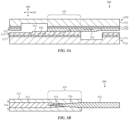
- FIG. 2A depicts a top view of a second example multi-chip photonic assembly 200
- FIG. 2B depicts a side view of the multi-chip photonic assembly 200 of FIG. 2A
- the multi-chip photonic assembly 200 includes a first photonic integrated circuit 210 coupled to a second photonic integrated circuit 220 in a flip chip arrangement.
- the first photonic integrated circuit 210 has a same area as that of the first photonic integrated circuit 110 shown in FIG. 1
- the second photonic integrated circuit 220 has a same area as that of the second photonic integrated circuit 120 of FIG. 1 .
- the overall footprint of the multi-chip photonic assembly 200 is significantly smaller than that of the multi-chip photonic assembly 100 of FIG. 1 .
- the first and second photonic integrated circuits 210, 220 in order for the first and second photonic integrated circuits 210, 220 to operate together, light must be transferred between them.
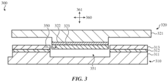
- FIG. 3 depicts a side view of a third example multi-chip photonic assembly 300.
- the multi-chip photonic assembly 300 may include a first photonic integrated circuit 310 (or a bottom chip) coupled to a second photonic integrated circuit 320 (or a top chip) stacked vertically (with respect to a vertical axis 361) in a flip chip arrangement, similar to the arrangement shown in FIGs. 2A-2B .
- the first photonic integrated circuit 310 may include a first substrate 311 (such as silicon), a first buried oxide layer 312, and a first waveguide 313.
- the second photonic integrated circuit 320 may include a second substrate 321 (such as silicon), a second buried oxide layer 322, and a second waveguide 323.
- buried oxide layer is intended to cover any buried low-index optical cladding layer made from any suitable material having lower refractive index than the waveguide material (or materials), only one example of which is silicon oxide.
- waveguides discussed herein may be made from silicon, a combination of materials such as a high-index material with a lower-index cladding (e.g., Si//SiO2, Si/SiN, or the like), and so on.
- first and/or second the photonic integrated circuits may optionally include one or more additional low-index optical cladding layers to provide optical confinement to the waveguides in one or more transverse directions.
- the first photonic integrated circuit 310 defines a cavity 351 such that the first waveguide 313 and the second waveguide 323 (which may both have a uniform vertical dimension) may occupy the same horizontal plane (with respect to a horizontal axis 360).
- Light 350 may be transmitted between the first waveguide 313 and the second waveguide 323, thus transmitting the light 350 between the first photonic integrated circuit 310 and the second photonic integrated circuit 320.
- Optically coupling directly between the first waveguide 313 and the second waveguide 323 in the same horizontal plane may be very optically efficient.
- optical losses may be less than 0.5 dB.
- the second photonic integrated circuit 320 protrudes into a cavity 351 defined in the first photonic integrated circuit 310 (or vice versa) in order to align the waveguides 313, 323. While this does transfer an optical signal between adjacent or bonded photonic integrated circuits, it does not change a layer or plane through which the optical signal propagates. Further, there is no footprint reduction of the first waveguide 313 and the second waveguide 323 when taken together, as they are necessarily the same horizontal plane. Since the optical signal does not propagate vertically (e.g., up or down the vertical axis 361 of FIG. 3 ), an overall footprint of the assembly may not be reduced.
- one or more mechanisms may be used that couple light between waveguides in two different horizontal planes of an assembly. Such mechanisms may operate as a "photonic via.”
- An "adiabatic butt coupler" implementation may use an adiabatic taper to gradually expand, in a vertical direction, the optical mode of a waveguide on a first chip. Once the mode is expanded, light may propagate across a small air gap (or filler gap, or the like) to a target waveguide with the same mode profile on another chip.
- Adiabatic butt couplers exhibit very low optical loss (e.g., little light is scattered or dissipated when coupling between waveguides), good tolerance with respect to misalignment between the chips, and broadband wavelength performance (e.g., a relatively large set of wavelengths of light may couple between waveguides).
- certain embodiments may coat an edge of either or both waveguides with an anti-reflection coating to reduce back-reflection of light.
- one or both waveguides may have an angled facet to reduce back-reflection.
- FIG. 4A is a side view of a fourth example multi-chip photonic assembly 400.
- the multi-chip photonic assembly 400 may implement a photonic via using an adiabatic butt coupler mechanism.
- the multi-chip photonic assembly 400 may include a first photonic integrated circuit 410 (or a bottom chip) coupled to a second photonic integrated circuit 420 (or a top chip), stacked vertically (with respect to a vertical axis 460) in a flip chip arrangement.
- the first photonic integrated circuit 410 may include a first substrate 411 (such as silicon), a first buried oxide layer 412, and a first waveguide 413 (such as a silicon waveguide).
- the second photonic integrated circuit 420 may include a second substrate 421 (such as silicon), a second buried oxide layer 422, and a second waveguide 423 (such as a silicon waveguide).
- the first and/or second photonic integrated circuit may optionally include additional low-index cladding layers (not shown) to provide optical confinement, such as depicted in FIG. 4D below.
- Light 450 (which may include one or more wavelengths, supporting either narrowband or broadband implementations) may be transmitted between the first waveguide 413 and the second waveguide 423, thus transmitting the light 450 between the first photonic integrated circuit 410 and the second photonic integrated circuit 420.
- the first waveguide 413 may have a first vertical dimension corresponding to a first region that is smaller in height than a second region 414 that has a second vertical dimension larger than the first dimension.
- the second waveguide 423 may have a third vertical dimension corresponding to a third region that is smaller in height than a fourth region 424 that has a fourth vertical dimension larger than the third dimension.
- the first region of the first waveguide 413 may occupy a different horizontal plane (with respect to a horizontal axis 461) than the third region of the second waveguide 423.
- the second region 414 of the first waveguide 413 may occupy a same and/or similar horizontal plane as the fourth region 424 of the second waveguide 423 such that the second region 414 and the fourth region 424 have vertical facets that face each other horizontally across a coupling gap 453.
- the mode of the light 450 may change, expanding corresponding to the larger vertical dimension of the second region 414.
- the light may then travel from the vertical facet of the second region 414 to the vertical facet of the fourth region 424 across the coupling gap 453.
- the light 450 may travel from a first side of the second waveguide 423 corresponding to the fourth region 424 to a second side of the second waveguide 423 corresponding to the third region (i.e., along the horizontal axis 461).
- the mode of the light 450 may change, shrinking as the larger vertical dimension of the fourth region 424 changes to the smaller vertical dimension of the third region of the second waveguide 423.
- the mode of the light 450 may change from the first horizontal plane of the first region of the first waveguide 413 to the second horizontal plane of the third region of the second waveguide 423.
- the light 450 travels in the vertical stacking direction (i.e., the vertical axis 460) by virtue of the second region 414 and the fourth region 424.
- FIG. 4B depicts a top view of the first photonic integrated circuit 410 removed from the multi-chip photonic assembly 400 of FIG. 4A .
- the first waveguide 413 may have a width 454 and the second region 414 may form an adiabatic taper.
- the adiabatic taper may taper from the second side of the first waveguide 413 corresponding to the second region 414 towards the first side of the first waveguide 413 corresponding to the first region.
- the width of the second region 414 decreases along the horizontal axis 461 from the second side of the first waveguide 413 toward the first side of the first waveguide 413 until the second region 414 terminates.
- This adiabatic taper may function to expand the mode of the light 450.
- the second region 414 may be one of the adiabatic butt couplers mentioned above.
- the second region 414 is shown in FIGs. 4A and 4B as having a uniform vertical dimension. However, it is understood that this is an example. In various implementations, the vertical dimension of the second region 414 may slope, curve, step, or otherwise vary from the vertical dimension of the first region of the first waveguide 413 to the maximum vertical dimension of the second region 414. Various configurations are possible and contemplated without departing from the scope of the present disclosure.
- FIG. 4C depicts a bottom view of the second photonic integrated circuit 420 removed from the multi-chip photonic assembly 400 of FIG. 4A with the second substrate 421 removed for clarity.
- the fourth region 424 may form an adiabatic taper.
- the adiabatic taper may taper from the second side of the second waveguide 423 corresponding to the fourth region 424 towards the first side of the second waveguide 423 corresponding to the third region.
- the width of the fourth region 424 decreases along the horizontal axis 461 from the second side of the second waveguide 423 toward the first side of the second waveguide 413 until the fourth region 424 terminates.
- This adiabatic taper may function to shrink the mode of the light 450.
- the fourth region 424 may be the other of the adiabatic butt couplers mentioned above.
- the coupling between the photonic circuits can be bidirectional, whereby light introduced into the second waveguide 423 is transferred to the first waveguide 413, in which case the adiabatic taper formed by the fourth region 424 will expand the mode of the light and the adiabatic taper formed by the second region 414 will shrink the mode of the light 450.
- the fourth region 424 is shown in FIGs. 4A and 4C as having a uniform vertical dimension. However, it is understood that this is an example. In various implementations, the vertical dimension of the fourth region 424 may slope, curve, step, or otherwise vary from the vertical dimension of the third region of the second waveguide 423 to the maximum vertical dimension of the fourth region 424. Various configurations are possible and contemplated without departing from the scope of the present disclosure.
- the first region of the first waveguide 413 may be separated from the second waveguide 423 by a gap 452 in the vertical direction.
- This gap 452 in the vertical direction may allow space for one or more layers of cladding materials (as mentioned above, such as oxide), air, one or more coupling structures (not shown) that couple the first photonic integrated circuit 410 to the second photonic integrated circuit 420 (such as one or more adhesives, epoxy or other underfills, pillar and bump configurations where one or more pillars configured on one of the first photonic integrated circuit 410 and the second photonic integrated circuit 420 (such as using one or more of the first waveguide 413 and/or the second waveguide 423 to form such pillars) connect to one or more gold or other solder bumps on the other of the first photonic integrated circuit 410 and second photonic integrated circuit 420 whereupon the solder bumps are reflowed to bond to the pillars, and so on) one or more anti-reflection coatings, and so on.
- cladding materials as mentioned above
- This gap 452 in the vertical direction may also prevent the first region of the first waveguide 413 from contacting the second waveguide 423. While the photonic integrated circuits 410 and 420 are shown in FIG. 4A as coupled in a flip chip arrangement, this does not require electrical connections to be made between the photonic integrated circuits. Electrical connections may be made between the photonic integrated circuits if desired (e.g., to allow electrical signal transmission between the photonic integrated circuits).
- an 8 micron height for the second vertical dimension of the second region 414 and the fourth vertical dimension of the fourth region 424 may allow for a 3 micron height for the first region of the first waveguide 413 and the third region of the second waveguide 423 and a 2 micron height for the gap 452 in the vertical direction (which may allow space for oxide and/or other cladding and/or other materials).
- the first photonic integrated circuit 410 defines a cavity 456 (a "first cavity").
- the cavity 456 extends at least partially through the first buried oxide layer 412 of the first photonic integrated circuit 410.
- the cavity 456 extends fully through the first buried oxide layer 412 and at least partially through the first substrate 411.
- the fourth region 424 of the second waveguide 423 extends at least partially into the cavity 456 of the first photonic integrated circuit 410. This allows a portion of the fourth region 424 of the second waveguide 423 to occupy the same horizontal plane (with respect to horizontal axis 461) as a portion of the first region of the first waveguide 413.
- the second photonic integrated circuit 420 defines a cavity 455 (a "second cavity").
- the cavity 455 extends at least partially through the second buried oxide layer 422 of the second photonic integrated circuit 420.
- the cavity 455 extends fully through the second buried oxide layer 422 and at least partially through the second substrate 421.
- the second region 414 of the first waveguide 413 extends at least partially into the cavity 455 of the second photonic integrated circuit 420. This allows a portion of the second region 414 of the first waveguide 413 to occupy the same horizontal plane (with respect to horizontal axis 461) as a portion of the third region of the second waveguide 423.
- the first photonic integrated circuit 410 and the second photonic integrated circuit 420 may each be fabricated by epitaxial growth and subsequent etching.
- a wafer may have a silicon substrate covered by a buried oxide layer, which is itself covered by a silicon layer (e.g., a 3-micron silicon layer). Silicon may be added by epitaxial growth prior to subsequent etching. Etching may be used to define the waveguides (e.g., first waveguide 413 and second waveguide 423) and cavities (e.g., cavities 455 and 456) of the multi-chip photonic assembly 400, such as described below with respect to FIGS. 7A-7E .
- Various configurations are possible and contemplated without departing from the scope of the present disclosure.
- This adiabatic butt coupler implementation illustrated and described above may use adiabatic transfer to expand and/or shrink the optical mode of the light 450 vertically.
- This implementation may provide a large first waveguide 413 and second waveguide 423 cross-section at the coupling gap 453, which may provide good tolerance for misalignment.
- misalignment may result in lossier light 450 transfer, causing parasitic and/or other light 450 modes that may be sources of noise. However, in some implementations, some such misalignment may be acceptable and/or otherwise accounted for.
- Various configurations are possible and contemplated without departing from the scope of the present disclosure.
- This adiabatic butt coupler implementation illustrated and described above may have low coupling loss (such as at least less than 1dB).
- This adiabatic taper may allow for very broadband performance.
- the large first waveguide 413 and second waveguide 423 may provide good tolerance for misalignment.
- the tapers may be fairly long, such as approximately 700 micrometers or more on each side of the coupling gap 453. Further, new silicon growth and etch may result in challenging fabrication.
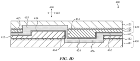
- FIG. 4D depicts a side view of an alternative implementation of the multi-chip photonic assembly 400 of FIG. 4A .
- one or more first cladding material layers 465 e.g., a material having a lower refractive index than the first waveguide 413, such as an oxide
- one or more second cladding material layers 462 e.g., a material having a lower refractive index than the first waveguide 413, such as an oxide
- These cladding layers may provide optical confinement to the first waveguide 413 and the second waveguide 423.
- the space between the first cladding material layer 465 and the second cladding material layer 462 may be filled by an underfill 463, such as an optically clear epoxy.
- the underfill 463 may mechanically couple the first photonic integrated circuit 410 and the second photonic integrated circuit 420.
- the second region 414 and the fourth region 424 have laterally angled facets that face each other (e.g., are non-perpendicular as they extend from a first side surface to another side surface, or in and out of the page as shown in FIG. 4D ), as well as one or more anti-reflective coatings 464 disposed upon those angled facets.
- vertically angled facets may be used in lieu of laterally angled facets (e.g., such facets are non-perpendicular as they extend from a base to a top surface, or from the top to the bottom of the page in FIG. 4D ).
- the first cladding material layers 465 may be applied to the entire surface of the first waveguide 413 and then portions may be selectively removed (such as any area where the light 450 is to pass, including along the vertical facet of the second region 414). In other implementations, the first cladding material layers 465 may be selectively applied to the portions of the surface of the first waveguide 413, such as using one or more masks, such that areas from which light is to exit the waveguide are not covered.
- the second cladding material layers 462 may be applied to the entire surface of the second waveguide 423 and then portions may be selectively removed (such as any area where the light 450 is to pass, including along the vertical facet of the fourth region 424). In other implementations, the second cladding material layers 462 may be selectively applied to the portions of the surface of the second waveguide 423, such as using one or more masks, such that areas from which light is to exit the waveguide are not covered.
- multi-chip photonic assembly 400 is illustrated and described as including particular components arranged in a particular manner with respect to FIGs. 4A-4C and/or 4D, it is understood that this is an example. In various implementations, other configurations are possible and contemplated without departing from the scope of the present disclosure.
- the multi-chip photonic assembly 400 is illustrated and described as coupling the first photonic integrated circuit 410 to the second photonic integrated circuit 420.
- any number of photonic integrated circuits may be coupled together, such as three, ten, and so on.
- Various configurations are possible and contemplated without departing from the scope of the present disclosure.
- each photonic integrated circuit (of multi-chip photonic assembly 400 as well as the other multi-chip photonic assemblies described herein) may include additional photonics components (e.g., splitters, multiplexers, outcouplers, additional waveguides) that are not shown here.
- the light 450 is illustrated and described as travelling from the first photonic integrated circuit 410 to the second photonic integrated circuit 420. However, it is understood that this is an example. In various examples, the light 450 may travel from the second photonic integrated circuit 420 to the first photonic integrated circuit 410. In still other examples, the light 450 may travel from the first photonic integrated circuit 410 to the second photonic integrated circuit 420 at some times and/or at some locations and from the second photonic integrated circuit 420 to the first photonic integrated circuit 410 at other times and/or other locations. Various configurations are possible and contemplated without departing from the scope of the present disclosure.
- the adiabatic taper of the second region 414 and the adiabatic taper of the fourth region 424 are illustrated as being the same length. However, it is understood that this is an example. In various implementations, the adiabatic taper of the second region 414 and the adiabatic taper of the fourth region 424 may have different lengths. Lengths of the adiabatic taper of the second region 414 and the adiabatic taper of the fourth region 424 may be wavelength and/or geometry dependent. Various configurations are possible and contemplated without departing from the scope of the present disclosure.
- a multi-chip photonic assembly may include a first photonic integrated circuit including a first waveguide having a first region that occupies a first horizontal plane and has a first vertical dimension and a second region that has a second vertical dimension that is larger than the first vertical dimension, the second region including a first adiabatic taper.
- the multi-chip photonic assembly may also include a second photonic integrated circuit, including a second waveguide, stacked vertically over the first photonic integrated circuit, the second waveguide having a third region that occupies a second horizontal plane and has a third vertical dimension and a fourth region that has a fourth vertical dimension that is larger than the third vertical dimension, the fourth region including a second adiabatic taper.
- the second region may be positioned in the second horizontal plane.
- the second region and the fourth region may change a mode of light travelling between the first photonic integrated circuit and the second photonic integrated circuit.
- the second region may overlap the fourth region in the first horizontal plane and the second horizontal plane.
- the multi-chip photonic assembly may further include an anti-reflection coating positioned between the second region and the fourth region.
- the first adiabatic taper may taper horizontally from a first side of the second region that faces the fourth region to a second side of the second region that is opposite the first side.
- the first adiabatic taper may taper vertically from a first side of the second region that faces the fourth region to a second side of the second region that is opposite the first side.
- the second region and the fourth region may cooperate to define a gap between the second region and the fourth region and the gap may be filled with at least one of air or an optically clear underfill.
- the second region may include a first angled facet and the fourth region may include a second angled facet that faces the first angled facet in the first horizontal plane and the second horizontal plane.
- An "adiabatic taper transfer" implementation may rely on direct contact between waveguides on two chips to transfer light. As the bottom waveguide is narrowed and the top waveguide is widened, the light may be directly transferred from the bottom waveguide to the top waveguide, without needing to propagate through any air gap. This implementation has the potential for very low loss, extremely broadband wavelength performance, and extremely low back-reflection.
- FIG. 5A depicts a side view of a fifth example multi-chip photonic assembly 500.
- the multi-chip photonic assembly 500 may implement a photonic via using an adiabatic taper transfer mechanism.
- the multi-chip photonic assembly 500 may include a first photonic integrated circuit 510 (or a bottom chip) coupled to a second photonic integrated circuit 520 (or a top chip) stacked vertically (with respect to a vertical axis 560) in a flip chip arrangement.
- the first photonic integrated circuit 510 may include a first substrate 511 (such as silicon), a first buried oxide layer 512, and a first waveguide 513 (such as a silicon waveguide).
- the second photonic integrated circuit 520 may include a second substrate 521 (such as silicon), a second buried oxide layer 522, and a second waveguide 523 (such as a silicon waveguide).
- Light 550 (which may include one or more wavelengths, supporting either narrowband or broadband implementations) may be transmitted between the first waveguide 513 and the second waveguide 523, thus transmitting the light 550 between the first photonic integrated circuit 510 and the second photonic integrated circuit 520.
- the first waveguide 513 may have a first vertical dimension corresponding to a first region that is smaller in height than a second region 514 that has a second vertical dimension larger than the first dimension.
- the second waveguide 523 may have a third vertical dimension corresponding to a third region that is smaller in height than a fourth region 524 that has a fourth vertical dimension larger than the third dimension.
- the first waveguide 513 may occupy a different horizontal plane (with respect to a horizontal axis 561) than the second waveguide 523. However, a portion of the second region 514 of the first waveguide 513 may vertically contact a portion of the fourth region 524 of the second waveguide 523 in an adiabatic transfer region 555.
- the portion of the second region 514 of the first waveguide 513 may still vertically contact the portion of the fourth region 524 of the second waveguide 523 in the adiabatic transfer region 555 if one or more optically clear adhesives and/or other optically clear materials are positioned therebetween.
- FIG. 5B depicts a top view of the multi-chip photonic assembly 500 of FIG. 5A with the second substrate 521 and the second buried oxide 522 of the second integrated circuit 520 removed for clarity.
- the first region of the first waveguide 513 may have a width 554 and the second region 514 and the fourth region 524 may each form an adiabatic taper.
- the adiabatic taper of the second region 514 may taper from the first side of the first waveguide 513 corresponding to the first region towards the second side of the first waveguide 513 corresponding to the second region 514.
- the adiabatic taper of the fourth region 524 may taper from the first side of the second waveguide 523 corresponding to the third region towards the second side of the second waveguide 523 corresponding to the fourth region 524.
- These adiabatic tapers may function to respectively expand and contract the mode of the light 550.
- the mode of the light 550 may change, expanding corresponding to the larger vertical dimension of the second region 514.
- the light 550 may be directly transferred from the first waveguide 513 to the second waveguide 523 without the need to propagate through any air gap (which may have very low loss, have extremely broadband wavelength performance, and have extremely low back-reflection).
- the light 550 may travel from a first side of the second waveguide 523 corresponding to the fourth region 524 to a second side of the second waveguide 523 corresponding to the third region.
- the mode of the light 550 may change, shrinking as the larger vertical dimension of the fourth region 524 changes to the smaller vertical dimension of the third region of the second waveguide 523. In this way, the mode of the light 550 may change from the first horizontal plane of the first region of the first waveguide 513 to the second horizontal plane of the third region of the second waveguide 523.
- the second region 514 is shown in FIGs. 5A and 5B as having a uniform vertical dimension. However, it is understood that this is an example. In various implementations, the vertical dimension of the second region 514 may slope, curve, step, or otherwise vary from the vertical dimension of the first region of the first waveguide 513 to the maximum vertical dimension of the second region 514. Various configurations are possible and contemplated without departing from the scope of the present disclosure.
- the fourth region 524 is shown in FIGs. 5A and 5B as having a uniform vertical dimension. However, it is understood that this is an example. In various implementations, the vertical dimension of the fourth region 524 may slope, curve, step, or otherwise vary from the vertical dimension of the third region of the second waveguide 523 to the maximum vertical dimension of the fourth region 524. Various configurations are possible and contemplated without departing from the scope of the present disclosure.
- the first region of the first waveguide 513 may be separated from the second waveguide 523 by a gap 552 in the vertical direction.
- This gap 552 in the vertical direction may allow space for one or more layers of cladding materials (such as oxide), air, one or more coupling structures (not shown) that couple the first photonic integrated circuit 510 to the second photonic integrated circuit 520 (such as one or more adhesives, epoxy or other underfills, pillar and bump configurations where one or more pillars configured on one of the first photonic integrated circuit 510 and the second photonic integrated circuit 520 (such as using one or more of the first waveguide 513 and/or the second waveguide 523 to form such pillars) connect to one or more gold or other solder bumps on the other of the first photonic integrated circuit 510 and second photonic integrated circuit 520 whereupon the solder bumps are reflowed to bond to the pillars, and so on) one or more anti-reflection coatings, and so on.
- a 4 micron height for the second vertical dimension of the second region 514 and the fourth vertical dimension of the fourth region 524 may allow for a 3 micron height for the first region of the first waveguide 513 and the third region of the second waveguide 523 and a 2 micron height for the gap 552 in the vertical direction (which may allow space for oxide cladding and/or other materials).
- the first photonic integrated circuit 510 and the second photonic integrated circuit 520 may be fabricated by epitaxial growth and subsequent etching.
- a wafer may have a silicon substrate covered by a buried oxide layer, which is itself covered by a 3-micron silicon layer. 1 micron of silicon may be added by epitaxial growth prior to subsequent etching.
- Various configurations are possible and contemplated without departing from the scope of the present disclosure.
- This adiabatic taper transfer implementation illustrated and described above may have low coupling loss (such as less than 1dB), allow for very broadband performance, and require relatively little epitaxial growth (such as epitaxial silicon growth) (such as 1 micron epitaxial growth compared to the 5 micron epitaxial growth for the adiabatic butt coupler implementation illustrated and discussed above).
- performance may be sensitive to the presence of any vertical gap between the second region 514 and the fourth region 524. For example, a 100-nanometer oxide gap may decrease transmission to less than 10 percent.
- this adiabatic taper transfer implementation may require fairly long adiabatic tapers, such as over 1000 micrometers.
- multi-chip photonic assembly 500 is illustrated and described as including particular components arranged in a particular manner with respect to FIGs. 5A-5B , it is understood that this is an example. In various implementations, other configurations are possible and contemplated without departing from the scope of the present disclosure.
- the multi-chip photonic assembly 500 is illustrated and described as coupling the first photonic integrated circuit 510 to the second photonic integrated circuit 520.
- any number of photonic integrated circuits may be coupled together, such as three, ten, and so on.
- Various configurations are possible and contemplated without departing from the scope of the present disclosure.
- the light 550 is illustrated and described as travelling from the first photonic integrated circuit 510 to the second photonic integrated circuit 520. However, it is understood that this is an example. In various examples, the light 550 may travel from the second photonic integrated circuit 520 to the first photonic integrated circuit 510. In still other examples, the light 550 may travel from the first photonic integrated circuit 510 to the second photonic integrated circuit 520 at some times and/or at some locations and from the second photonic integrated circuit 520 to the first photonic integrated circuit 510 at other times and/or other locations. Various configurations are possible and contemplated without departing from the scope of the present disclosure.
- the adiabatic taper of the second region 514 and the adiabatic taper of the fourth region 524 are illustrated as being the same length. However, it is understood that this is an example. In various implementations, the adiabatic taper of the second region 514 and the adiabatic taper of the fourth region 524 may have different lengths. Lengths of the adiabatic taper of the second region 514 and the adiabatic taper of the fourth region 524 may be wavelength and/or geometry dependent. Various configurations are possible and contemplated without departing from the scope of the present disclosure.
- a multi-chip photonic assembly may include a first photonic integrated circuit including a first waveguide having a first region that occupies a first horizontal plane and has a first vertical dimension and a second region that has a second vertical dimension that is larger than the first vertical dimension, the second region having a first adiabatic taper.
- the multi-chip photonic assembly may also include a second photonic integrated circuit, including a second waveguide, stacked vertically over the first photonic integrated circuit, the second waveguide having a third region that occupies a second horizontal plane and has a third vertical dimension and a fourth region that has a fourth vertical dimension that is larger than the third vertical dimension, the fourth region including a second adiabatic taper.
- the second region may vertically contact the second waveguide.
- the second region and the fourth region may change a mode of light travelling between the first photonic integrated circuit and the second photonic integrated circuit.
- the second region may vertically contact the second waveguide via an optically clear adhesive.
- the multi-chip photonic assembly may further include an adiabatic transfer region where the second adiabatic taper vertically overlaps the first adiabatic taper.
- the light may travel between the first waveguide and the second waveguide where the second region vertically contacts the second waveguide.
- the multi-chip photonic assembly may further include cladding material positioned between the first waveguide and the second waveguide.
- the first adiabatic taper may taper opposite the second adiabatic taper.
- the second region may be positioned proximate the fourth region and opposite the third region.
- a vertical multi-mode interference coupler implementation may rely on interference between optical modes to transfer light.
- the input optical mode on a bottom plane may be imaged to the mirror location on a top plane after propagating a certain distance, and then the light may propagate across a small air gap to reach the target waveguide on the other chip.
- This implementation has a potential for very low loss and good tolerance to misalignment between the chips. Back-reflections at the gap can be minimized using anti-reflection coatings and angled facets.
- FIG. 6A depicts a side view of a sixth example multi-chip photonic assembly 600.
- the multi-chip photonic assembly 600 may implement a photonic via using a vertical multi-mode interference coupler mechanism.
- the multi-chip photonic assembly 600 may include a first photonic integrated circuit 610 (or a bottom chip) coupled to a second photonic integrated circuit 620 (or a top chip) stacked vertically (with respect to a vertical axis 660) in a flip chip arrangement.
- the first photonic integrated circuit 610 may include a first substrate 611 (such as silicon), a first buried oxide layer 612, and a first waveguide 613 (such as a silicon waveguide).
- the second photonic integrated circuit 620 may include a second substrate 621 (such as silicon), a first buried oxide layer 622, and a second waveguide 623 (such as a silicon waveguide).
- Light 650 (which may include one or more wavelengths) may be transmitted between the first waveguide 613 and the second waveguide 623, thus transmitting the light 650 between the first photonic integrated circuit 610 and the second photonic integrated circuit 620.
- the first waveguide 613 may have a first vertical dimension corresponding to a first region that is smaller in height than a second region 614 that has a second vertical dimension larger than the first dimension.
- the second waveguide 623 may have a third vertical dimension.
- the first region of the first waveguide 613 may occupy a different horizontal plane (with respect to a horizontal axis 661) than the second waveguide 623.
- the second region 614 of the first waveguide 613 may occupy a same and/or similar horizontal plane as the second waveguide 623 such that the second region 614 and the second waveguide 623 have vertical facets that face each other horizontally across a coupling gap 653.
- the height change in the first waveguide 613 from the first region to the second region 614 will split the light into multiple optical modes.
- the second region 614 is sized such that interference between the optical modes may cause input optical mode on a bottom plane of the second region 614 to be imaged to the mirror location on a top plane of the second region 614 after propagating a certain distance through the second region 614.
- the light 650 may then propagate across a coupling gap 653 to reach the second waveguide 623.
- the light 650 may travel from a first side of the second waveguide 623 proximate the coupling gap 653 to a second side of the second waveguide 623 opposite the first side. In this way, the mode of the light 650 may change from the first horizontal plane of the first region of the first waveguide 613 to the second horizontal plane of the second waveguide 623.
- FIG. 6B depicts a top view of the first photonic integrated circuit 610 removed from the multi-chip photonic assembly 600 of FIG. 6A .
- the first waveguide 613 may have a width 654, which may be measured in single-digit micrometers.
- the second region 614 may have a uniform horizontal dimension extending from a first side of the second region 614 (that faces the second waveguide 623) to a second side of the second region 614 that is opposite the first side.
- the second region 614 is shown in FIGs. 6A and 6B as having a uniform vertical dimension. However, it is understood that this is an example. In various implementations, the vertical dimension of the second region 614 may slope, curve, step, or otherwise vary from the vertical dimension of the first region of the first waveguide 613 to the maximum vertical dimension of the second region 614. Various configurations are possible and contemplated without departing from the scope of the present disclosure.
- FIG. 6C depicts a bottom view of the second photonic integrated circuit 620 removed from the multi-chip photonic assembly 600 of FIG. 4A with the second substrate 621 removed for clarity.
- the first region of the first waveguide 613 may be separated from the second waveguide 623 by a gap 652 in the vertical direction.
- This gap 652 in the vertical direction may allow space for one or more layers of cladding materials (e.g., a material having a lower refractive index than the waveguides, such as an oxide), air, one or more coupling structures (not shown) that couple the first photonic integrated circuit 610 to the second photonic integrated circuit 620 (such as one or more adhesives, epoxy or other underfills, pillar and bump configurations where one or more pillars configured on one of the first photonic integrated circuit 610 and the second photonic integrated circuit 620 (such as using one or more of the first waveguide 613 and/or the second waveguide 623 to form such pillars) connect to one or more gold or other solder bumps on the other of the first photonic integrated circuit 610 and second photonic integrated circuit 620 whereupon the solder bumps are reflowed to bond to the pillars, and so on
- h min represents the minimum height of the second region 614
- 2h strip represents twice the height of the first region of the first waveguide 613
- vertical gap represents the gap 652 in the vertical direction.
- an 8 micron height for the second vertical dimension of the second region 614 and the fourth vertical dimension of the fourth region 624 may allow for a 3 micron height for the first region of the first waveguide 613 and the second waveguide 623 and a 2 micron height for the gap 652 in the vertical direction (which may allow space for oxide cladding and/or other materials).
- the second photonic integrated circuit 620 defines a cavity 655.
- the cavity 655 extends at least partially through the first buried oxide layer 622 of the second photonic integrated circuit 620. In the variation shown in FIG. 6A , the cavity 655 extends fully through the first buried oxide layer 622 and at least partially through the second substrate 621.
- the second region 614 of the first waveguide 613 extends at least partially into the cavity 655 of the second photonic integrated circuit 620. This allows a portion of the second region 614 of the first waveguide 613 to occupy the same horizontal plane (with respect to horizontal axis 661) as a portion of the second waveguide 623.
- the first photonic integrated circuit 610 may be fabricated by epitaxial growth and subsequent etching.
- a wafer may have a silicon substrate covered by a buried oxide layer, which is itself covered by a 3-micron silicon layer. Silicon may be added by epitaxial growth prior to subsequent etching.
- Various configurations are possible and contemplated without departing from the scope of the present disclosure.
- This multi-mode interference coupler implementation illustrated and described above may rely on multi-mode interference to move the optical mode of the light 650 to a different plane. Relatively large cross-sections of the first waveguide 613 at the coupling gap 653 may provide good tolerance to misalignment. Peak transmission may be quite high, such as with less than 1dB loss.
- multi-mode interference may be a narrowband device. Higher bandwidths may increase loss and multi-mode interference may be used pre-multiplexer (and/or a multiplexer may be used to narrow the band prior to the multi-mode interference coupler and a demultiplexer may be used to widen the band after the multi-mode interference coupler). Further, new silicon growth and etch may result in challenging fabrication.
- misalignment may result in lossier light 650 transfer, causing parasitic and/or other light 650 modes that may be sources of noise. However, in some implementations, some such misalignment may be acceptable and/or otherwise accounted for.
- Various configurations are possible and contemplated without departing from the scope of the present disclosure.
- multi-chip photonic assembly 600 is illustrated and described as including particular components arranged in a particular manner with respect to FIGs. 6A-6C , it is understood that this is an example. In various implementations, other configurations are possible and contemplated without departing from the scope of the present disclosure.
- the multi-chip photonic assembly 600 is illustrated and described as coupling the first photonic integrated circuit 610 to the second photonic integrated circuit 620.
- any number of photonic integrated circuits may be coupled together, such as three, ten, and so on.
- Various configurations are possible and contemplated without departing from the scope of the present disclosure.
- the light 650 is illustrated and described as travelling from the first photonic integrated circuit 610 to the second photonic integrated circuit 620. However, it is understood that this is an example. In various examples, the light 650 may travel from the second photonic integrated circuit 620 to the first photonic integrated circuit 610. In still other examples, the light 650 may travel from the first photonic integrated circuit 610 to the second photonic integrated circuit 620 at some times and/or at some locations and from the second photonic integrated circuit 620 to the first photonic integrated circuit 610 at other times and/or other locations. Various configurations are possible and contemplated without departing from the scope of the present disclosure.
- a multi-chip photonic assembly may include a first photonic integrated circuit including a first waveguide having a first region that occupies a first horizontal plane and has a first vertical dimension and a second region that has a second vertical dimension that is larger than the first vertical dimension.
- the multi-chip photonic assembly may further include a second photonic integrated circuit, including a second waveguide that occupies a second horizontal plane, stacked vertically over the first photonic integrated circuit.
- the second region may be positioned in the second horizontal plane. The second region may change a mode of light travelling between the first photonic integrated circuit and the second photonic integrated circuit.
- the second region may use interference between optical modes to transfer the light travelling between the first photonic integrated circuit and the second photonic integrated circuit.
- the second region may have a uniform horizontal dimension from a first side of the second region that faces the second waveguide to a second side of the second region that is opposite the first side.
- the second vertical dimension may be uniform from a first side of the second region that faces the second waveguide to a second side of the second region that is opposite the first side.
- the first waveguide may define a gap horizontally between the second region and the second waveguide.
- the second waveguide may have a third vertical dimension that is smaller than the second vertical dimension.
- FIGs. 7A-7E illustrate fabrication of a photonic integrated circuit.
- FIG. 7A depicts an example wafer for a photonic integrated circuit.
- the wafer may be used to make one or more of the first photonic integrated circuits 410, 510, 610, 802 and/or the second photonic integrated circuits 420, 520, 620, 804 of FIGs. 1-6C and 8A-8C .
- the wafer may include a substrate 711 (such as a silicon substrate), a buried oxide layer 712, and a layer 713 (such as a silicon layer).
- the buried oxide layer 712 may be one micrometer in height and the layer 713 may be a three micrometer layer of silicon, although these are example measurements and provided by way of illustration. Actual measurements may vary in different embodiments.
- FIG. 7B depicts the example wafer of FIG. 7A after performance of an epitaxial growth operation. This may result in epitaxial growth of the layer 713, thereby providing a thicker layer for processing and feature formation.
- FIG. 7C depicts the wafer of FIG. 7B after performance of a first etching operation.
- the first etching operation may remove portions of the layer 713 in order to leave a portion of the layer 713 proud of the rest of the surface.
- FIG. 7D depicts the wafer of FIG. 7C after performance of a second etching operation.
- This second etching operation may remove entire areas of the layer 713, exposing one or more portions of the buried oxide layer 712.
- FIG. 7E depicts the wafer of FIG. 7D after performance of a deep cavity etching operation.
- This deep cavity etching operation may remove entire areas of the buried oxide layer 712 and/or portions of the substrate 711.
- Additional operations may be performed subsequent to FIG. 7E .
- Such additional operations may include one or more backend processing steps, flip chip bonding, and so on.
- backend processing steps flip chip bonding, and so on.
- flip chip bonding flip chip bonding
- FIG. 8A shows a side view of a sixth example multi-chip photonic assembly 800. Similar to the multi-chip photonic assembly 400 described above with respect to FIGS. 4A-4D , the multi-chip photonic assembly 800 vertically expands the mode of light before it is transferred between photonics integrated circuits. Instead of using a taper (that expands toward a facet of a waveguide) to vertically expand the mode in the multi-chip photonic assembly 400, the multi-chip photonic assembly 800 expands the mode using a waveguide segment made from two different waveguide materials.
- the multi-chip photonic assembly 800 may include a first photonic integrated circuit 802 (or a bottom chip) coupled to a second photonic integrated circuit 804 (or a top chip), stacked vertically (with respect to a vertical axis 860) in a flip chip arrangement.
- the first photonic integrated circuit 802 may include a first substrate 810 (such as silicon), a first waveguide 806, and a first buried oxide layer 808 between the first substrate 810 and the first waveguide 806.
- the second photonic integrated circuit 804 may include a second substrate 826 (such as silicon) a second waveguide 822, and a second buried oxide layer 824 between the second substrate 826 and the second waveguide 822.
- the first and/or second photonic integrated circuit may optionally include additional low-index cladding layers (not shown) that have a lower refractive index than the materials of the first and second waveguides, which thereby provide optical confinement as discussed above.
- Light 850 (which is depicted in FIGS. 8B and 8C and may include one or more wavelengths, supporting either narrowband or broadband implementations) may be transmitted between the first waveguide 806 and the second waveguide 822, thus transmitting the light 850 between the first photonic integrated circuit 802 and the second photonic integrated circuit 804.
- FIG. 8B depicts a top view of the first photonic integrated circuit 802 removed from the multi-chip photonic assembly 800 of FIG. 8A .
- the first waveguide 806 is formed from a first waveguide material (e.g., silicon) that is partially overlaid by a second waveguide material (e.g., silicon mononitride, a polymer, or the like) having a lower refractive index than the first waveguide material.
- the first waveguide 806 comprises a first region connected to a second region (i.e., a distal end of the first region is coupled to a proximal end of the second region).
- the first region is formed from a first segment 814 of the first waveguide material (also referred to as "first segment 814") and the second region is formed from a second segment 816 of the first waveguide material (also referred to as “second segment 816") and a segment 818 of the second waveguide material (also referred to as "fifth segment 818") that covers the second segment 816.
- the first segment 814 and the second segment 816 may be formed as a monolithic component, and in these instances interface between the first region and second region is defined by the addition of the segment 818 of the second waveguide material to the second region.
- the fifth segment 818 is taller than the second segment 816 and is at least as wide, such that the exterior dimensions of the fifth segment 818 define the exterior dimensions of the second region.
- the first region has a vertical dimension (a "first vertical dimension") that is smaller in height than a vertical dimension of the second region (a "second vertical dimension”).
- the second region has a width that is greater the first region.
- These dimensions may also determine the dimensions of a vertical facet 820 at a distal end of the first waveguide 806.
- the first segment 814 has a width (a "first width") where the first region meets the second region (i.e., at a distal end of the first region).
- the second segment 816 tapers adiabatically in the second region, such that the width of the second segment 816 narrows from the first width (in a direction from a proximal end of the second region toward the distal end/vertical facet of the second region).
- the second segment 816 terminates prior to the distal end of the second region.
- the vertical facet 820 at the distal end of the second region is formed entirely from the segment 818 of the second waveguide material.
- FIG. 8C depicts a top view of the second photonic integrated circuit 804 removed from the multi-chip photonic assembly 800 of FIG. 8A .
- the second waveguide 822 is formed from a third waveguide material (e.g., silicon) that is partially overlaid by a fourth waveguide material (e.g., silicon mononitride, a polymer, or the like) having a lower refractive index than the third waveguide material.
- the first waveguide material from the first waveguide 806) may be the same material as or a different material from the third waveguide material (from the second waveguide 822).
- the second waveguide material (from the first waveguide 806) may be the same material as or a different material from the fourth waveguide material (from the second waveguide).
- the second waveguide 808 comprises a third region connected to a fourth region (i.e., a distal end of the third region is coupled to a proximal end of the fourth region).
- the third region is formed from a first segment 830 of the third waveguide material (also referred to as "third segment 830") and the fourth region is formed from a second segment 832 of the third waveguide material (also referred to as "fourth segment 832") and a segment 834 of the fourth waveguide material (also referred to as "sixth segment 834”) that covers the fourth segment 832.
- the third segment 830 and the fourth segment 832 may be formed as a monolithic component, and in these instances interface between the third region and fourth region is defined by the addition of the segment 834 of the fourth waveguide material to the fourth region.
- the sixth segment 834 is taller than the fourth segment 832 and is at least as wide, such that the exterior dimensions of the sixth segment 834 define the exterior dimensions of the fourth region.
- the third region has a vertical dimension (a "third vertical dimension") that is smaller in height than a vertical dimension of the fourth region (a "fourth vertical dimension”). In some instances, the fourth region has a width that is greater the third region. These dimensions may also determine the dimensions of a vertical facet 836 at a distal end of the second waveguide 822.
- the third segment 814 has a width (a "second width", which may be the same as or different from the first width) where the third region meets the fourth region (i.e., at a distal end of the third region).
- the fourth segment 816 tapers adiabatically in the fourth region, such that the width of the fourth segment 816 narrows from the second width (in a direction from a proximal end of the fourth region toward the distal end/vertical facet of the fourth region). In some instances, the fourth segment 816 terminates prior to the distal end of the fourth region. In these instances, the vertical facet 836 at the distal end of the second region is formed entirely from the segment 818 of the second waveguide material.
- the distal end of the first waveguide 806 faces the distal end of the second waveguide 822.
- the fifth segment 818 may occupy a common horizontal plane (with respect to horizontal axis 861) as the sixth segment 834.
- the first segment 814 and second segment 816 of the first waveguide material are positioned in a different horizontal plane (with respect to the horizontal axis 861) than the third segment 830 and fourth segment 832 of the third waveguide material.
- the first waveguide 806 As light 850 is introduced into the first waveguide 806 (e.g., at a proximal end of the first waveguide), light travels from the first region the second region along the first waveguide material. As the light 850 passes from the first segment 814 to the second segment 816, the narrowing width of the second segment 816 may no longer be able to confine the light 850, resulting in the mode expanding into the second waveguide material (i.e., the fifth segment 818). As the mode expands, the second waveguide material will act to confine the light 850. The light will travel through the second waveguide material in the second region until it reaches the vertical facet 820 of the first waveguide 806.
- the light will cross gap 838 from the vertical facet 820 of the first waveguide 806 to the vertical facet 836 of the second waveguide 822. From there, the light 850 is confined by and travels through the fourth waveguide material (i.e., the sixth segment 834) in the fourth region. As the width of the fourth segment 832 increases (i.e., toward the proximal end of the fourth region), the light 850 will begin to couple into and be confined by the third waveguide material (thereby shrinking the mode). As the light 850 reaches the proximal end of the fourth region, the light 850 may be fully confined by the third waveguide material.
- the fourth waveguide material i.e., the sixth segment 834
- the light 850 may enter the second waveguide 822 through the sixth segment 834, couple into the fourth segment 832 of third waveguide material, and then pass into the third segment 830 of third waveguide material. In this way, the light 850 may be transferred from a proximal end of the first waveguide 806 to a proximal end of the second waveguide 822. Similarly, light introduced into proximal end of the second waveguide 822 may be transferred to a proximal end of the first waveguide 806. This results in the light being passed form a first horizontal plane in one photonic integrated circuit to a different horizontal plane in the other photonic integrated circuit.
- the second region of the first waveguide 806 and the fourth region of the second waveguide 822 are shown in FIG. 8A as having a uniform vertical dimension, in some instances the second region and/or fourth regions have a vertical dimension that varies.
- the height of the fifth segment 818 (and thus the height of the second region) may slope, curve, step, or otherwise vary from the vertical dimension of the first region to the maximum vertical dimension of the second region.
- the height of the sixth segment 834 (and thus the height of the fourth region) may slope, curve, step, or otherwise vary from the vertical dimension of the third region to the maximum vertical dimension of the fourth region.
- the first photonic integrated circuit 802 may be vertically separated from the second photonic integrated circuit 802 to allow space for one or more layers of cladding materials (as mentioned above, such as oxide), air, one or more coupling structures (such as one or more adhesives, epoxy or other underfills, pillar and bump configurations as discussed above), between the waveguides of the different photonic integrated circuits. While the photonic integrated circuits 802 and 804 are shown in FIG. 8A as coupled in a flip chip arrangement, this does not require electrical connections to be made between the photonic integrated circuits. Electrical connections may be made between the photonic integrated circuits if desired (e.g., to allow electrical signal transmission between the photonic integrated circuits).
- cladding materials as oxide
- coupling structures such as one or more adhesives, epoxy or other underfills, pillar and bump configurations as discussed above
- the first photonic integrated circuit 802 defines a cavity 812.
- the cavity 812 extends at least partially through the first buried oxide layer 808 of the first photonic integrated circuit 802.
- the cavity 812 extends fully through the first buried oxide layer 808 and at least partially through the first substrate 810.
- the fourth region of the second waveguide 822 (specifically the sixth segment 834) extends at least partially into the cavity 812 of the first photonic integrated circuit 802. This allows a portion of the fourth region of the second waveguide 822 to occupy the same horizontal plane (with respect to horizontal axis 861) as a portion of the first region of the first waveguide 806.
- the second photonic integrated circuit 804 defines a cavity 828.
- the cavity 828 extends at least partially through the second buried oxide layer 824 of the second photonic integrated circuit 804.
- the cavity 828 extends fully through the second buried oxide layer 824 and at least partially through the second substrate 826.
- the first photonic integrated circuit 802 and the second photonic integrated circuit 804 may be fabricated such as discussed above (e.g., with epitaxial growth and subsequent etching), with the additional step of depositing and etching the additional waveguide material.
- First and second photonic integrated circuits having first and second waveguides may be vertically stacked such that first vertical dimensions of the first and second waveguides occupy different horizontal planes in the stack. At least one of the first and second waveguides has a region that has a second vertical dimension that is larger than the first vertical dimension and either horizontally overlaps the other waveguide and/or vertically contacts the other waveguide. Light moving through one of the waveguides from the first vertical dimension to the other vertical dimension changes modes vertically so that the light moves from one waveguide to the other.
Landscapes
- Physics & Mathematics (AREA)
- General Physics & Mathematics (AREA)
- Optics & Photonics (AREA)
- Engineering & Computer Science (AREA)
- Microelectronics & Electronic Packaging (AREA)
- Power Engineering (AREA)
- Optical Integrated Circuits (AREA)
Abstract
There is provided a multi-chip photonic assembly, comprising: a first photonic integrated circuit (410) including a first waveguide (413) having: a first region that occupies a first horizontal plane and has a first vertical dimension; and a second region (414) that has a second vertical dimension that is larger than the first vertical dimension, the second region comprising a first adiabatic taper; and a second photonic integrated circuit (420), including a second waveguide (423), stacked vertically over the first photonic integrated circuit, the second waveguide (423) having: a third region that occupies a second horizontal plane and has a third vertical dimension; and a fourth region (424) that has a fourth vertical dimension that is larger than the third vertical dimension, the fourth region comprising a second adiabatic taper; wherein: the second region (414) is positioned in the second horizontal plane; and the second region (414) and the fourth region (424) change a mode of light (450) travelling between the first photonic integrated circuit (410) and the second photonic integrated circuit (420).
Description
- This application claims the benefit under 35 U.S. C. § 119(e) of
U.S. Provisional Patent Application No. 63/247,726, filed September 23, 2021 U.S. Provisional Patent Application No. 63/310,397, filed February 15, 2022 - The described embodiments relate generally to photonic integrated circuits. More particularly, the present embodiments relate to mechanisms that transfer light between photonic integrated circuits.
- Microelectronics relates to manufacture (or microfabrication) of very small electronic designs and components. One example of such devices, digital integrated circuits, may be made from semiconductor materials and may include components like transistors, capacitors, inductors, resistors, diodes, insulators, and conductors. Wiring techniques like wire bonding are often used in digital integrated circuits and other microelectronics because of the unusually small size of the components, leads, and pads. Various techniques may be used to connect multiple digital integrated circuits in order to build complex systems.
- Some typical integrated circuits may be multi-layer circuits, where electrical signals are routed through traces on opposing sides of a single substrate or on traces defined on various stacked substrates. Vias may extend through a substrate to permit electrical signals to travel from one layer or substrate or side to another. Generally, such vias are formed from a copper fill.
- Photonic integrated circuits (or integrated optical circuits) are devices that integrate certain photonic functions, generally replacing electrical signals with photonic (e.g., light-based) signals. In certain ways, photonic integrated circuits are similar to a digital integrated circuit. The major difference between photonic integrated circuits and a digital integrated circuit is that a photonic integrated circuit utilizes light as a signal medium rather than electricity, which in turn requires the use of optical components rather than conventional circuitry. While electrical signals may change layers by propagating through electrical vias in typical integrated circuits, there are few such options for optical signals of a photonic integrated circuit. Thus, optical signals are typically routed in a single layer or plane of such a circuit, constraining design options.
- The present disclosure relates to multi-chip photonic assemblies. First and second photonic integrated circuits having first and second waveguides may be vertically stacked such that first vertical dimensions of the first and second waveguides occupy different horizontal planes in the stack. At least one of the first and second waveguides has a region that has a second vertical dimension that is larger than the first vertical dimension and either horizontally overlaps the other waveguide and/or vertically contacts the other waveguide. Light moving through one of the waveguides from the first vertical dimension to the other vertical dimension changes modes vertically so that the light moves from one waveguide to the other.
- In various embodiments, a multi-chip photonic assembly includes a first photonic integrated circuit including a first waveguide having a first region that occupies a first horizontal plane and has a first vertical dimension and a second region that has a second vertical dimension that is larger than the first vertical dimension, the second region including a first adiabatic taper. The multi-chip photonic assembly also includes a second photonic integrated circuit, including a second waveguide, stacked vertically over the first photonic integrated circuit, the second waveguide having a third region that occupies a second horizontal plane and has a third vertical dimension and a fourth region that has a fourth vertical dimension that is larger than the third vertical dimension, the fourth region including a second adiabatic taper. The second region is positioned in the second horizontal plane. The second region and the fourth region change a mode of light travelling between the first photonic integrated circuit and the second photonic integrated circuit.
- In some examples, the second region overlaps the fourth region in the first horizontal plane and the second horizontal plane. In various implementations of such examples, the multi-chip photonic assembly further includes an anti-reflection coating positioned between the second region and the fourth region. In some implementations of such examples, the first adiabatic taper tapers horizontally from a first side of the second region that faces the fourth region to a second side of the second region that is opposite the first side. In a number of implementations of such examples, the first adiabatic taper tapers vertically from a first side of the second region that faces the fourth region to a second side of the second region that is opposite the first side. In some implementations of such examples, the second region and the fourth region cooperate to define a gap between the second region and the fourth region and the gap is filled with at least one of air or an optically clear underfill.
- In a number of examples, the second region includes a first angled facet and the fourth region includes a second angled facet that faces the first angled facet in the first horizontal plane and the second horizontal plane.
- In some embodiments, a multi-chip photonic assembly includes a first photonic integrated circuit including a first waveguide having a first region that occupies a first horizontal plane and has a first vertical dimension and a second region that has a second vertical dimension that is larger than the first vertical dimension, the second region having a first adiabatic taper. The multi-chip photonic assembly also includes a second photonic integrated circuit, including a second waveguide, stacked vertically over the first photonic integrated circuit, the second waveguide having a third region that occupies a second horizontal plane and has a third vertical dimension and a fourth region that has a fourth vertical dimension that is larger than the third vertical dimension, the fourth region including a second adiabatic taper. The second region vertically contacts the second waveguide. The second region and the fourth region change a mode of light travelling between the first photonic integrated circuit and the second photonic integrated circuit.
- In various examples, the second region vertically contacts the second waveguide via an optically clear adhesive. In some examples, the multi-chip photonic assembly further includes an adiabatic transfer region where the second adiabatic taper vertically overlaps the first adiabatic taper. In various implementations of such examples, the light travels between the first waveguide and the second waveguide where the second region vertically contacts the second waveguide.
- In some examples, the multi-chip photonic assembly further includes cladding material positioned between the first waveguide and the second waveguide. In a number of examples, the first adiabatic taper tapers opposite the second adiabatic taper. In some examples, the second region is positioned proximate the fourth region and opposite the third region.
- In a number of embodiments, a multi-chip photonic assembly includes a first photonic integrated circuit including a first waveguide having a first region that occupies a first horizontal plane and has a first vertical dimension and a second region that has a second vertical dimension that is larger than the first vertical dimension. The multi-chip photonic assembly further includes a second photonic integrated circuit, including a second waveguide that occupies a second horizontal plane, stacked vertically over the first photonic integrated circuit. The second region is positioned in the second horizontal plane. The second region changes a mode of light travelling between the first photonic integrated circuit and the second photonic integrated circuit.
- In various examples, the second region uses interference between optical modes to transfer the light travelling between the first photonic integrated circuit and the second photonic integrated circuit. In some examples, the second region has a uniform horizontal dimension from a first side of the second region that faces the second waveguide to a second side of the second region that is opposite the first side. In a number of examples, the second vertical dimension is uniform from a first side of the second region that faces the second waveguide to a second side of the second region that is opposite the first side. In various examples, the first waveguide defines a gap horizontally between the second region and the second waveguide. In some examples, the second waveguide has a third vertical dimension that is smaller than the second vertical dimension.
- In various examples a multi-chip photonic assembly includes a first photonic integrated circuit having a first waveguide, the first waveguide having a first region that occupies a first horizontal plane and has a first vertical dimension and a second region that has a second vertical dimension that is larger than the first vertical dimension. The second region includes a first waveguide material and a second waveguide material overlaying the first waveguide material and having a lower refractive index than the first waveguide material. The multi-chip photonic assembly also includes a second photonic integrated circuit having a second waveguide and stacked vertically over the first photonic integrated circuit. The second waveguide has a third region that occupies a second horizontal plane and has a third vertical dimension and a fourth region that has a fourth vertical dimension that is larger than the third vertical dimension. The fourth region includes a third waveguide material and a fourth waveguide material overlaying third first waveguide material and having a lower refractive index than the third waveguide material. The second region is positioned in the second horizontal plane, and the second region and the fourth region change a mode of light travelling between the first photonic integrated circuit and the second photonic integrated circuit.
- In some examples, the first region includes a first segment of the first waveguide material, the second region includes a second segment of the first waveguide material, and a width of the second segment tapers adiabatically in the second region. Additionally or alternatively, the third region includes a third segment of the third waveguide material, the second region includes a fourth segment of the fourth waveguide material, and a width of the fourth segment tapers adiabatically in the fourth region. In some instances, the second segment terminates prior to a distal end of the second region. Additionally or alternatively, the fourth segment terminates prior to a distal end of the fourth region.
- In a number of examples, the first waveguide material and the third waveguide material are the same material. Additionally or alternatively, the second waveguide material and the fourth waveguide material are the same material. In some examples, the first photonic integrated circuit defines a cavity and the fourth region extends at least partially into the cavity of the first photonic device. Additionally or alternatively, the second photonic integrated circuit defines a cavity and the second region extends at least partially into the cavity of the second photonic device.
- The disclosure will be readily understood by the following detailed description in conjunction with the accompanying drawings, wherein like reference numerals designate like structural elements.
-
FIG. 1 depicts a top view of a first example multi-chip photonic assembly. -
FIG. 2A depicts a top view of a second example multi-chip photonic assembly. -
FIG. 2B depicts a side view of the multi-chip photonic assembly ofFIG. 2A . -
FIG. 3 depicts a side view of a third example multi-chip photonic assembly. -
FIG. 4A depicts a side view of a fourth example multi-chip photonic assembly. -
FIG. 4B depicts a top view of the first photonic integrated circuit removed from the multi-chip photonic assembly ofFIG. 4A . -
FIG. 4C depicts a bottom view of the second photonic integrated circuit removed from the multi-chip photonic assembly ofFIG. 4A with the substrate removed for clarity. -
FIG. 4D depicts a side view of an alternative implementation of the multi-chip photonic assembly ofFIG. 4A . -
FIG. 5A depicts a side view of a fifth example multi-chip photonic assembly. -
FIG. 5B depicts a top view of the multi-chip photonic assembly ofFIG. 5A with the substrate and the buried oxide of the second integrated circuit removed for clarity. -
FIG. 6A depicts a side view of a sixth example multi-chip photonic assembly. -
FIG. 6B depicts a top view of the first photonic integrated circuit removed from the multi-chip photonic assembly ofFIG. 6A . -
FIG. 6C depicts a bottom view of the second photonic integrated circuit removed from the multi-chip photonic assembly ofFIG. 6A with the substrate removed for clarity. -
FIG. 7A depicts an example wafer for a photonic integrated circuit. The wafer may be used to make one or more of the first photonic integrated circuits and/or the second photonic integrated circuits ofFIGS. 1-6C andFIGS. 8A-8C . -
FIG. 7B depicts the example wafer ofFIG. 7A after performance of an epitaxial growth operation. -
FIG. 7C depicts the wafer ofFIG. 7B after performance of a first etching operation. -
FIG. 7D depicts the wafer ofFIG. 7C after performance of a second etching operation. -
FIG. 7E depicts the wafer ofFIG. 7D after performance of a deep cavity etching operation. -
FIG. 8A depicts a side view of a seventh example multi-chip photonic assembly. -
FIG. 8B depicts a top view of the multi-chip photonic assembly ofFIG. 8A , with the second photonic chip removed for clarity. -
FIG. 8C depicts a bottom view of the multi-chip photonic assembly ofFIG. 8A , with the first photonic chip removed for clarity. - Reference will now be made in detail to representative embodiments illustrated in the accompanying drawings. It should be understood that the following descriptions are not intended to limit the embodiments to one preferred embodiment. To the contrary, it is intended to cover alternatives, modifications, and equivalents as can be included within the spirit and scope of the described embodiments as defined by the appended claims.
- The description that follows includes sample systems, methods, and apparatuses that embody various elements of the present disclosure. However, it should be understood that the described disclosure may be practiced in a variety of forms in addition to those described herein.
- The ability to flexibly connect multiple digital integrated circuit chips together may be critical for building complex systems in microelectronics. Having similar flexibility for photonic integrated circuits, such as flip chip or side by side arrangements, may also be valuable. By way of illustration, splitting of the functionality of a photonic integrated circuit between two or more chips in a flip chip configuration may lead to a much smaller overall footprint, which may be especially important for mobile or wearable applications where space may be extremely limited. This may also increase modularity, providing photonic system designers the flexibility to mix and match different components, which may be useful for applications like rapid prototyping or optimal wavelength binning during manufacturing. Splitting up functionality may also open up new fabrication possibilities, since different chips could be run with separate, potentially incompatible process flows.
- For example, a photonic integrated circuit may include a Mach-Zehnder interferometer, an Echelle grating, and an optical phased array passive delay line network. The optical phased array passive delay line network may occupy a relatively large area of the photonic integrated circuit. By splitting the photonic integrated circuit into a first photonic integrated circuit having the Mach-Zehnder interferometer and the Echelle grating and a second photonic integrated circuit having the optical phased array passive delay line network couplable to the first photonic circuit in a flip chip or other arrangement, a much smaller overall footprint may be achieved.
- By way of another example, a photonic integrated circuit may include a first wafer having a first crystalline orientation and a second wafer having a second crystalline orientation. As the two orientations are different, the two wafers are separate from one another. However, light may pass from one wafer (or one component on that wafer) to the other wafer (or a second component on that wafer) as part of the operation of the photonic integrated circuit. Embodiments described herein may facilitate the use of wafers with different crystalline orientations in the same multi-chip photonic assembly by simplifying light transmission therebetween, while conserving space of the overall assembly.
- In yet another example, a photonic integrated circuit may include a laser and a grating that need to be have their optical wavelengths precisely matched. Splitting the laser and the grating onto different photonic integrated circuits may enable optimal wavelength binning of the laser and the grating during manufacturing to enable use of photonic integrated circuits including lasers to be used with photonic integrated circuits including gratings that appropriately match the lasers.
- In still another example, splitting components of a photonic integrated circuit into multiple photonic integrated circuits may increase yield. This may be due to the fact that a component that does not meet one or more sets of requirements or standards may cause only the respective photonic integrated circuit to include that component as opposed to the photonic integrated circuit that includes all of the components.
- One of the main challenges of multi-chip architectures in photonics is that it is difficult to transfer light from one chip to another without losing a large amount of the light. The present disclosure may address this issue by providing mechanisms to transfer light between photonic chips, such as in a flip chip arrangement, without incurring large optical losses.
- The following disclosure relates to multi-chip photonic assemblies. First and second photonic integrated circuits having first and second waveguides may be vertically stacked such that first portions (having first vertical dimensions) of the first and second waveguides occupy different horizontal planes in the stack. At least one of the first and second waveguides has a region with a second vertical dimension that is larger than the first vertical dimension; this second vertical dimension either horizontally overlaps the other waveguide and/or vertically contacts the other waveguide. Light moving through one of the waveguides from the first vertical dimension to the other vertical dimension changes modes vertically so that the light moves from one waveguide to the other.
- These and other embodiments are discussed below with reference to
FIGS. 1-8C . However, those skilled in the art will readily appreciate that the detailed description given herein with respect to these Figures is for explanatory purposes only and should not be construed as limiting. -
FIG. 1 depicts a top view of a first example multi-chipphotonic assembly 100. The multi-chipphotonic assembly 100 includes a first photonicintegrated circuit 110 coupled to a second photonicintegrated circuit 120 in a side by side arrangement. As the first photonicintegrated circuit 110 and the second photonic integratedcircuit 120 are coupled side by side, the overall footprint of the multi-chipphotonic assembly 100 is the same as the overall footprint of the first photonicintegrated circuit 110 plus that of the second photonic integratedcircuit 120. -
FIG. 2A depicts a top view of a second example multi-chipphotonic assembly 200, whileFIG. 2B depicts a side view of the multi-chipphotonic assembly 200 ofFIG. 2A . With respect toFIGs. 2A and 2B , the multi-chipphotonic assembly 200 includes a first photonicintegrated circuit 210 coupled to a second photonicintegrated circuit 220 in a flip chip arrangement. Generally and for example comparative purposes, the first photonicintegrated circuit 210 has a same area as that of the first photonicintegrated circuit 110 shown inFIG. 1 , and the second photonic integratedcircuit 220 has a same area as that of the second photonic integratedcircuit 120 ofFIG. 1 . As the first photonicintegrated circuit 210 and the second photonic integratedcircuit 220 are stacked vertically (e.g., with one atop the other), the overall footprint of the multi-chipphotonic assembly 200 is significantly smaller than that of the multi-chipphotonic assembly 100 ofFIG. 1 . However, in order for the first and second photonicintegrated circuits -
FIG. 3 depicts a side view of a third example multi-chipphotonic assembly 300. The multi-chipphotonic assembly 300 may include a first photonic integrated circuit 310 (or a bottom chip) coupled to a second photonic integrated circuit 320 (or a top chip) stacked vertically (with respect to a vertical axis 361) in a flip chip arrangement, similar to the arrangement shown inFIGs. 2A-2B . The first photonicintegrated circuit 310 may include a first substrate 311 (such as silicon), a firstburied oxide layer 312, and afirst waveguide 313. Similarly, the second photonic integratedcircuit 320 may include a second substrate 321 (such as silicon), a secondburied oxide layer 322, and asecond waveguide 323. Generally, the term "buried oxide layer," as used herein, is intended to cover any buried low-index optical cladding layer made from any suitable material having lower refractive index than the waveguide material (or materials), only one example of which is silicon oxide. Similarly, waveguides discussed herein may be made from silicon, a combination of materials such as a high-index material with a lower-index cladding (e.g., Si//SiO2, Si/SiN, or the like), and so on. In other words first and/or second the photonic integrated circuits may optionally include one or more additional low-index optical cladding layers to provide optical confinement to the waveguides in one or more transverse directions. - The first photonic
integrated circuit 310 defines acavity 351 such that thefirst waveguide 313 and the second waveguide 323 (which may both have a uniform vertical dimension) may occupy the same horizontal plane (with respect to a horizontal axis 360).Light 350 may be transmitted between thefirst waveguide 313 and thesecond waveguide 323, thus transmitting the light 350 between the first photonicintegrated circuit 310 and the second photonic integratedcircuit 320. - Optically coupling directly between the
first waveguide 313 and thesecond waveguide 323 in the same horizontal plane may be very optically efficient. For example, optical losses may be less than 0.5 dB. - However, as the
first waveguide 313 and thesecond waveguide 323 are in the same horizontal plane, the second photonic integratedcircuit 320 protrudes into acavity 351 defined in the first photonic integrated circuit 310 (or vice versa) in order to align thewaveguides first waveguide 313 and thesecond waveguide 323 when taken together, as they are necessarily the same horizontal plane. Since the optical signal does not propagate vertically (e.g., up or down thevertical axis 361 ofFIG. 3 ), an overall footprint of the assembly may not be reduced. - In order to achieve a footprint reduction, one or more mechanisms may be used that couple light between waveguides in two different horizontal planes of an assembly. Such mechanisms may operate as a "photonic via."
- An "adiabatic butt coupler" implementation may use an adiabatic taper to gradually expand, in a vertical direction, the optical mode of a waveguide on a first chip. Once the mode is expanded, light may propagate across a small air gap (or filler gap, or the like) to a target waveguide with the same mode profile on another chip. Adiabatic butt couplers exhibit very low optical loss (e.g., little light is scattered or dissipated when coupling between waveguides), good tolerance with respect to misalignment between the chips, and broadband wavelength performance (e.g., a relatively large set of wavelengths of light may couple between waveguides). Further, certain embodiments may coat an edge of either or both waveguides with an anti-reflection coating to reduce back-reflection of light. Similarly, one or both waveguides may have an angled facet to reduce back-reflection.
- As one example of the foregoing,
FIG. 4A is a side view of a fourth example multi-chipphotonic assembly 400. The multi-chipphotonic assembly 400 may implement a photonic via using an adiabatic butt coupler mechanism. - The multi-chip
photonic assembly 400 may include a first photonic integrated circuit 410 (or a bottom chip) coupled to a second photonic integrated circuit 420 (or a top chip), stacked vertically (with respect to a vertical axis 460) in a flip chip arrangement. The first photonicintegrated circuit 410 may include a first substrate 411 (such as silicon), a firstburied oxide layer 412, and a first waveguide 413 (such as a silicon waveguide). Similarly, the second photonic integratedcircuit 420 may include a second substrate 421 (such as silicon), a secondburied oxide layer 422, and a second waveguide 423 (such as a silicon waveguide). The first and/or second photonic integrated circuit may optionally include additional low-index cladding layers (not shown) to provide optical confinement, such as depicted inFIG. 4D below. Light 450 (which may include one or more wavelengths, supporting either narrowband or broadband implementations) may be transmitted between thefirst waveguide 413 and thesecond waveguide 423, thus transmitting the light 450 between the first photonicintegrated circuit 410 and the second photonic integratedcircuit 420. - The
first waveguide 413 may have a first vertical dimension corresponding to a first region that is smaller in height than asecond region 414 that has a second vertical dimension larger than the first dimension. Similarly, thesecond waveguide 423 may have a third vertical dimension corresponding to a third region that is smaller in height than afourth region 424 that has a fourth vertical dimension larger than the third dimension. The first region of thefirst waveguide 413 may occupy a different horizontal plane (with respect to a horizontal axis 461) than the third region of thesecond waveguide 423. However, thesecond region 414 of thefirst waveguide 413 may occupy a same and/or similar horizontal plane as thefourth region 424 of thesecond waveguide 423 such that thesecond region 414 and thefourth region 424 have vertical facets that face each other horizontally across acoupling gap 453. - As the light 450 travels from a first side of the
first waveguide 413 corresponding to the first region (i.e., along the horizontal axis 461) to a second side of thefirst waveguide 413 corresponding to thesecond region 414, the mode of the light 450 may change, expanding corresponding to the larger vertical dimension of thesecond region 414. The light may then travel from the vertical facet of thesecond region 414 to the vertical facet of thefourth region 424 across thecoupling gap 453. From there, the light 450 may travel from a first side of thesecond waveguide 423 corresponding to thefourth region 424 to a second side of thesecond waveguide 423 corresponding to the third region (i.e., along the horizontal axis 461). As the light 450 so travels, the mode of the light 450 may change, shrinking as the larger vertical dimension of thefourth region 424 changes to the smaller vertical dimension of the third region of thesecond waveguide 423. In this way, the mode of the light 450 may change from the first horizontal plane of the first region of thefirst waveguide 413 to the second horizontal plane of the third region of thesecond waveguide 423. In other words, the light 450 travels in the vertical stacking direction (i.e., the vertical axis 460) by virtue of thesecond region 414 and thefourth region 424. -
FIG. 4B depicts a top view of the first photonicintegrated circuit 410 removed from the multi-chipphotonic assembly 400 ofFIG. 4A . As shown, thefirst waveguide 413 may have awidth 454 and thesecond region 414 may form an adiabatic taper. The adiabatic taper may taper from the second side of thefirst waveguide 413 corresponding to thesecond region 414 towards the first side of thefirst waveguide 413 corresponding to the first region. In other words, the width of thesecond region 414 decreases along thehorizontal axis 461 from the second side of thefirst waveguide 413 toward the first side of thefirst waveguide 413 until thesecond region 414 terminates. This adiabatic taper may function to expand the mode of the light 450. In this way, thesecond region 414 may be one of the adiabatic butt couplers mentioned above. - The
second region 414 is shown inFIGs. 4A and 4B as having a uniform vertical dimension. However, it is understood that this is an example. In various implementations, the vertical dimension of thesecond region 414 may slope, curve, step, or otherwise vary from the vertical dimension of the first region of thefirst waveguide 413 to the maximum vertical dimension of thesecond region 414. Various configurations are possible and contemplated without departing from the scope of the present disclosure. -
FIG. 4C depicts a bottom view of the second photonic integratedcircuit 420 removed from the multi-chipphotonic assembly 400 ofFIG. 4A with thesecond substrate 421 removed for clarity. As shown, thefourth region 424 may form an adiabatic taper. The adiabatic taper may taper from the second side of thesecond waveguide 423 corresponding to thefourth region 424 towards the first side of thesecond waveguide 423 corresponding to the third region. In other words, the width of thefourth region 424 decreases along thehorizontal axis 461 from the second side of thesecond waveguide 423 toward the first side of thesecond waveguide 413 until thefourth region 424 terminates. This adiabatic taper may function to shrink the mode of the light 450. In this way, thefourth region 424 may be the other of the adiabatic butt couplers mentioned above. The coupling between the photonic circuits can be bidirectional, whereby light introduced into thesecond waveguide 423 is transferred to thefirst waveguide 413, in which case the adiabatic taper formed by thefourth region 424 will expand the mode of the light and the adiabatic taper formed by thesecond region 414 will shrink the mode of the light 450. - The
fourth region 424 is shown inFIGs. 4A and 4C as having a uniform vertical dimension. However, it is understood that this is an example. In various implementations, the vertical dimension of thefourth region 424 may slope, curve, step, or otherwise vary from the vertical dimension of the third region of thesecond waveguide 423 to the maximum vertical dimension of thefourth region 424. Various configurations are possible and contemplated without departing from the scope of the present disclosure. - With reference again to
FIG. 4A , the first region of thefirst waveguide 413 may be separated from thesecond waveguide 423 by agap 452 in the vertical direction. Thisgap 452 in the vertical direction may allow space for one or more layers of cladding materials (as mentioned above, such as oxide), air, one or more coupling structures (not shown) that couple the first photonicintegrated circuit 410 to the second photonic integrated circuit 420 (such as one or more adhesives, epoxy or other underfills, pillar and bump configurations where one or more pillars configured on one of the first photonicintegrated circuit 410 and the second photonic integrated circuit 420 (such as using one or more of thefirst waveguide 413 and/or thesecond waveguide 423 to form such pillars) connect to one or more gold or other solder bumps on the other of the first photonicintegrated circuit 410 and second photonicintegrated circuit 420 whereupon the solder bumps are reflowed to bond to the pillars, and so on) one or more anti-reflection coatings, and so on. Thisgap 452 in the vertical direction may also prevent the first region of thefirst waveguide 413 from contacting thesecond waveguide 423. While the photonicintegrated circuits FIG. 4A as coupled in a flip chip arrangement, this does not require electrical connections to be made between the photonic integrated circuits. Electrical connections may be made between the photonic integrated circuits if desired (e.g., to allow electrical signal transmission between the photonic integrated circuits). - The second vertical dimension of the
second region 414 and the fourth vertical dimension of thefourth region 424 may have a minimum height. This may be represented by the equation hmin = 2hstrip + vertical gap where hmin represents the minimum height of thesecond region 414 or thefourth region 424, 2hstrip represents twice the height of the other portion of the respective waveguide (i.e., the first region of thefirst waveguide 413 for thesecond region 414 and the third region of thesecond waveguide 423 for the fourth region 424), and "vertical gap" represents thegap 452. For example, an 8 micron height for the second vertical dimension of thesecond region 414 and the fourth vertical dimension of thefourth region 424 may allow for a 3 micron height for the first region of thefirst waveguide 413 and the third region of thesecond waveguide 423 and a 2 micron height for thegap 452 in the vertical direction (which may allow space for oxide and/or other cladding and/or other materials). - To accommodate the fourth vertical dimension of the
fourth region 424, the first photonicintegrated circuit 410 defines a cavity 456 (a "first cavity"). Thecavity 456 extends at least partially through the firstburied oxide layer 412 of the first photonicintegrated circuit 410. In the variation shown inFIG. 4A , thecavity 456 extends fully through the firstburied oxide layer 412 and at least partially through thefirst substrate 411. When the first photonicintegrated circuit 410 and the second photonic integratedcircuit 420 are vertically stacked as shown inFIG. 4A , thefourth region 424 of thesecond waveguide 423 extends at least partially into thecavity 456 of the first photonicintegrated circuit 410. This allows a portion of thefourth region 424 of thesecond waveguide 423 to occupy the same horizontal plane (with respect to horizontal axis 461) as a portion of the first region of thefirst waveguide 413. - Similarly, to accommodate the second vertical dimension of the
second region 414, the second photonic integratedcircuit 420 defines a cavity 455 (a "second cavity"). Thecavity 455 extends at least partially through the secondburied oxide layer 422 of the second photonic integratedcircuit 420. In the variation shown inFIG. 4A , thecavity 455 extends fully through the secondburied oxide layer 422 and at least partially through thesecond substrate 421. When the first photonicintegrated circuit 410 and the second photonic integratedcircuit 420 are vertically stacked as shown inFIG. 4A , thesecond region 414 of thefirst waveguide 413 extends at least partially into thecavity 455 of the second photonic integratedcircuit 420. This allows a portion of thesecond region 414 of thefirst waveguide 413 to occupy the same horizontal plane (with respect to horizontal axis 461) as a portion of the third region of thesecond waveguide 423. - The first photonic
integrated circuit 410 and the second photonic integratedcircuit 420 may each be fabricated by epitaxial growth and subsequent etching. For example, a wafer may have a silicon substrate covered by a buried oxide layer, which is itself covered by a silicon layer (e.g., a 3-micron silicon layer). Silicon may be added by epitaxial growth prior to subsequent etching. Etching may be used to define the waveguides (e.g.,first waveguide 413 and second waveguide 423) and cavities (e.g.,cavities 455 and 456) of the multi-chipphotonic assembly 400, such as described below with respect toFIGS. 7A-7E . Various configurations are possible and contemplated without departing from the scope of the present disclosure. - This adiabatic butt coupler implementation illustrated and described above may use adiabatic transfer to expand and/or shrink the optical mode of the light 450 vertically. This implementation may provide a large
first waveguide 413 andsecond waveguide 423 cross-section at thecoupling gap 453, which may provide good tolerance for misalignment. - Although the above discusses tolerance for misalignment, it is understood that this is an example. Misalignment may result in lossier light 450 transfer, causing parasitic and/or other light 450 modes that may be sources of noise. However, in some implementations, some such misalignment may be acceptable and/or otherwise accounted for. Various configurations are possible and contemplated without departing from the scope of the present disclosure.
- This adiabatic butt coupler implementation illustrated and described above may have low coupling loss (such as at least less than 1dB). This adiabatic taper may allow for very broadband performance. The large
first waveguide 413 andsecond waveguide 423 may provide good tolerance for misalignment. However, the tapers may be fairly long, such as approximately 700 micrometers or more on each side of thecoupling gap 453. Further, new silicon growth and etch may result in challenging fabrication. -
FIG. 4D depicts a side view of an alternative implementation of the multi-chipphotonic assembly 400 ofFIG. 4A . In this alternative implementation, one or more first cladding material layers 465 (e.g., a material having a lower refractive index than thefirst waveguide 413, such as an oxide) are positioned on thefirst waveguide 413 facing thesecond waveguide 423 and one or more second cladding material layers 462 (e.g., a material having a lower refractive index than thefirst waveguide 413, such as an oxide) are positioned on thesecond waveguide 423 facing thefirst waveguide 413. These cladding layers may provide optical confinement to thefirst waveguide 413 and thesecond waveguide 423. The space between the firstcladding material layer 465 and the secondcladding material layer 462 may be filled by anunderfill 463, such as an optically clear epoxy. Theunderfill 463 may mechanically couple the first photonicintegrated circuit 410 and the second photonic integratedcircuit 420. - Additionally or alternatively, the
second region 414 and thefourth region 424 have laterally angled facets that face each other (e.g., are non-perpendicular as they extend from a first side surface to another side surface, or in and out of the page as shown inFIG. 4D ), as well as one or moreanti-reflective coatings 464 disposed upon those angled facets. It should be appreciated that vertically angled facets may be used in lieu of laterally angled facets (e.g., such facets are non-perpendicular as they extend from a base to a top surface, or from the top to the bottom of the page inFIG. 4D ). - In some implementations, the first cladding material layers 465 may be applied to the entire surface of the
first waveguide 413 and then portions may be selectively removed (such as any area where the light 450 is to pass, including along the vertical facet of the second region 414). In other implementations, the first cladding material layers 465 may be selectively applied to the portions of the surface of thefirst waveguide 413, such as using one or more masks, such that areas from which light is to exit the waveguide are not covered. - Similarly, in some implementations, the second cladding material layers 462 may be applied to the entire surface of the
second waveguide 423 and then portions may be selectively removed (such as any area where the light 450 is to pass, including along the vertical facet of the fourth region 424). In other implementations, the second cladding material layers 462 may be selectively applied to the portions of the surface of thesecond waveguide 423, such as using one or more masks, such that areas from which light is to exit the waveguide are not covered. - Although the multi-chip
photonic assembly 400 is illustrated and described as including particular components arranged in a particular manner with respect toFIGs. 4A-4C and/or 4D, it is understood that this is an example. In various implementations, other configurations are possible and contemplated without departing from the scope of the present disclosure. - By way of example, the multi-chip
photonic assembly 400 is illustrated and described as coupling the first photonicintegrated circuit 410 to the second photonic integratedcircuit 420. However, in various implementations, any number of photonic integrated circuits may be coupled together, such as three, ten, and so on. Various configurations are possible and contemplated without departing from the scope of the present disclosure. Additionally, each photonic integrated circuit (of multi-chipphotonic assembly 400 as well as the other multi-chip photonic assemblies described herein) may include additional photonics components (e.g., splitters, multiplexers, outcouplers, additional waveguides) that are not shown here. - By way of another example, the light 450 is illustrated and described as travelling from the first photonic
integrated circuit 410 to the second photonic integratedcircuit 420. However, it is understood that this is an example. In various examples, the light 450 may travel from the second photonic integratedcircuit 420 to the first photonicintegrated circuit 410. In still other examples, the light 450 may travel from the first photonicintegrated circuit 410 to the second photonic integratedcircuit 420 at some times and/or at some locations and from the second photonic integratedcircuit 420 to the first photonicintegrated circuit 410 at other times and/or other locations. Various configurations are possible and contemplated without departing from the scope of the present disclosure. - In yet another example, the adiabatic taper of the
second region 414 and the adiabatic taper of thefourth region 424 are illustrated as being the same length. However, it is understood that this is an example. In various implementations, the adiabatic taper of thesecond region 414 and the adiabatic taper of thefourth region 424 may have different lengths. Lengths of the adiabatic taper of thesecond region 414 and the adiabatic taper of thefourth region 424 may be wavelength and/or geometry dependent. Various configurations are possible and contemplated without departing from the scope of the present disclosure. - In various implementations, a multi-chip photonic assembly may include a first photonic integrated circuit including a first waveguide having a first region that occupies a first horizontal plane and has a first vertical dimension and a second region that has a second vertical dimension that is larger than the first vertical dimension, the second region including a first adiabatic taper. The multi-chip photonic assembly may also include a second photonic integrated circuit, including a second waveguide, stacked vertically over the first photonic integrated circuit, the second waveguide having a third region that occupies a second horizontal plane and has a third vertical dimension and a fourth region that has a fourth vertical dimension that is larger than the third vertical dimension, the fourth region including a second adiabatic taper. The second region may be positioned in the second horizontal plane. The second region and the fourth region may change a mode of light travelling between the first photonic integrated circuit and the second photonic integrated circuit.
- In some examples, the second region may overlap the fourth region in the first horizontal plane and the second horizontal plane. In various such examples, the multi-chip photonic assembly may further include an anti-reflection coating positioned between the second region and the fourth region. In some such examples, the first adiabatic taper may taper horizontally from a first side of the second region that faces the fourth region to a second side of the second region that is opposite the first side. In a number of such examples, the first adiabatic taper may taper vertically from a first side of the second region that faces the fourth region to a second side of the second region that is opposite the first side. In some such examples, the second region and the fourth region may cooperate to define a gap between the second region and the fourth region and the gap may be filled with at least one of air or an optically clear underfill.
- In a number of examples, the second region may include a first angled facet and the fourth region may include a second angled facet that faces the first angled facet in the first horizontal plane and the second horizontal plane.
- An "adiabatic taper transfer" implementation may rely on direct contact between waveguides on two chips to transfer light. As the bottom waveguide is narrowed and the top waveguide is widened, the light may be directly transferred from the bottom waveguide to the top waveguide, without needing to propagate through any air gap. This implementation has the potential for very low loss, extremely broadband wavelength performance, and extremely low back-reflection.
- For example,
FIG. 5A depicts a side view of a fifth example multi-chipphotonic assembly 500. The multi-chipphotonic assembly 500 may implement a photonic via using an adiabatic taper transfer mechanism. - The multi-chip
photonic assembly 500 may include a first photonic integrated circuit 510 (or a bottom chip) coupled to a second photonic integrated circuit 520 (or a top chip) stacked vertically (with respect to a vertical axis 560) in a flip chip arrangement. The first photonic integrated circuit 510 may include a first substrate 511 (such as silicon), a firstburied oxide layer 512, and a first waveguide 513 (such as a silicon waveguide). Similarly, the second photonic integratedcircuit 520 may include a second substrate 521 (such as silicon), a secondburied oxide layer 522, and a second waveguide 523 (such as a silicon waveguide). Light 550 (which may include one or more wavelengths, supporting either narrowband or broadband implementations) may be transmitted between thefirst waveguide 513 and thesecond waveguide 523, thus transmitting the light 550 between the first photonic integrated circuit 510 and the second photonic integratedcircuit 520. - The
first waveguide 513 may have a first vertical dimension corresponding to a first region that is smaller in height than asecond region 514 that has a second vertical dimension larger than the first dimension. Similarly, thesecond waveguide 523 may have a third vertical dimension corresponding to a third region that is smaller in height than afourth region 524 that has a fourth vertical dimension larger than the third dimension. Thefirst waveguide 513 may occupy a different horizontal plane (with respect to a horizontal axis 561) than thesecond waveguide 523. However, a portion of thesecond region 514 of thefirst waveguide 513 may vertically contact a portion of thefourth region 524 of thesecond waveguide 523 in anadiabatic transfer region 555. The portion of thesecond region 514 of thefirst waveguide 513 may still vertically contact the portion of thefourth region 524 of thesecond waveguide 523 in theadiabatic transfer region 555 if one or more optically clear adhesives and/or other optically clear materials are positioned therebetween. -
FIG. 5B depicts a top view of the multi-chipphotonic assembly 500 ofFIG. 5A with thesecond substrate 521 and the secondburied oxide 522 of the secondintegrated circuit 520 removed for clarity. As shown, the first region of thefirst waveguide 513 may have awidth 554 and thesecond region 514 and thefourth region 524 may each form an adiabatic taper. The adiabatic taper of thesecond region 514 may taper from the first side of thefirst waveguide 513 corresponding to the first region towards the second side of thefirst waveguide 513 corresponding to thesecond region 514. Similarly, the adiabatic taper of thefourth region 524 may taper from the first side of thesecond waveguide 523 corresponding to the third region towards the second side of thesecond waveguide 523 corresponding to thefourth region 524. These adiabatic tapers may function to respectively expand and contract the mode of the light 550. - With respect to
FIGs. 5A and 5B , as the light 550 travels from a first side of thefirst waveguide 513 corresponding to the first region to a second side of thefirst waveguide 513 corresponding to thesecond region 514, the mode of the light 550 may change, expanding corresponding to the larger vertical dimension of thesecond region 514. As thesecond region 514 narrows and thefourth region 524 widens, the light 550 may be directly transferred from thefirst waveguide 513 to thesecond waveguide 523 without the need to propagate through any air gap (which may have very low loss, have extremely broadband wavelength performance, and have extremely low back-reflection). From there, the light 550 may travel from a first side of thesecond waveguide 523 corresponding to thefourth region 524 to a second side of thesecond waveguide 523 corresponding to the third region. As the light 550 so travels, the mode of the light 550 may change, shrinking as the larger vertical dimension of thefourth region 524 changes to the smaller vertical dimension of the third region of thesecond waveguide 523. In this way, the mode of the light 550 may change from the first horizontal plane of the first region of thefirst waveguide 513 to the second horizontal plane of the third region of thesecond waveguide 523. - The
second region 514 is shown inFIGs. 5A and 5B as having a uniform vertical dimension. However, it is understood that this is an example. In various implementations, the vertical dimension of thesecond region 514 may slope, curve, step, or otherwise vary from the vertical dimension of the first region of thefirst waveguide 513 to the maximum vertical dimension of thesecond region 514. Various configurations are possible and contemplated without departing from the scope of the present disclosure. - The
fourth region 524 is shown inFIGs. 5A and 5B as having a uniform vertical dimension. However, it is understood that this is an example. In various implementations, the vertical dimension of thefourth region 524 may slope, curve, step, or otherwise vary from the vertical dimension of the third region of thesecond waveguide 523 to the maximum vertical dimension of thefourth region 524. Various configurations are possible and contemplated without departing from the scope of the present disclosure. - With reference again to
FIG. 5A , the first region of thefirst waveguide 513 may be separated from thesecond waveguide 523 by agap 552 in the vertical direction. Thisgap 552 in the vertical direction may allow space for one or more layers of cladding materials (such as oxide), air, one or more coupling structures (not shown) that couple the first photonic integrated circuit 510 to the second photonic integrated circuit 520 (such as one or more adhesives, epoxy or other underfills, pillar and bump configurations where one or more pillars configured on one of the first photonic integrated circuit 510 and the second photonic integrated circuit 520 (such as using one or more of thefirst waveguide 513 and/or thesecond waveguide 523 to form such pillars) connect to one or more gold or other solder bumps on the other of the first photonic integrated circuit 510 and second photonicintegrated circuit 520 whereupon the solder bumps are reflowed to bond to the pillars, and so on) one or more anti-reflection coatings, and so on. Thisgap 552 in the vertical direction may also prevent the first region of thefirst waveguide 513 from contacting thesecond waveguide 523. - The second vertical dimension of the
second region 514 and the fourth vertical dimension of thefourth region 524 may have a minimum height. This may be represented by the equation hmin = strip + vertical gap/2 where hmin represents the minimum height of thesecond region 514 or thefourth region 524, hstrip represents the height of the other portion of the respective waveguide (i.e., the first region of thefirst waveguide 513 for thesecond region 514 and the third region of thesecond waveguide 523 for the fourth region 524), and vertical gap/2 represents half of thegap 552 in the vertical direction. For example, a 4 micron height for the second vertical dimension of thesecond region 514 and the fourth vertical dimension of thefourth region 524 may allow for a 3 micron height for the first region of thefirst waveguide 513 and the third region of thesecond waveguide 523 and a 2 micron height for thegap 552 in the vertical direction (which may allow space for oxide cladding and/or other materials). - The first photonic integrated circuit 510 and the second photonic integrated
circuit 520 may be fabricated by epitaxial growth and subsequent etching. For example, a wafer may have a silicon substrate covered by a buried oxide layer, which is itself covered by a 3-micron silicon layer. 1 micron of silicon may be added by epitaxial growth prior to subsequent etching. Various configurations are possible and contemplated without departing from the scope of the present disclosure. - This adiabatic taper transfer implementation illustrated and described above may have low coupling loss (such as less than 1dB), allow for very broadband performance, and require relatively little epitaxial growth (such as epitaxial silicon growth) (such as 1 micron epitaxial growth compared to the 5 micron epitaxial growth for the adiabatic butt coupler implementation illustrated and discussed above). However, performance may be sensitive to the presence of any vertical gap between the
second region 514 and thefourth region 524. For example, a 100-nanometer oxide gap may decrease transmission to less than 10 percent. Further, this adiabatic taper transfer implementation may require fairly long adiabatic tapers, such as over 1000 micrometers. - Although the multi-chip
photonic assembly 500 is illustrated and described as including particular components arranged in a particular manner with respect toFIGs. 5A-5B , it is understood that this is an example. In various implementations, other configurations are possible and contemplated without departing from the scope of the present disclosure. - By way of example, the multi-chip
photonic assembly 500 is illustrated and described as coupling the first photonic integrated circuit 510 to the second photonic integratedcircuit 520. However, in various implementations, any number of photonic integrated circuits may be coupled together, such as three, ten, and so on. Various configurations are possible and contemplated without departing from the scope of the present disclosure. - By way of another example, the light 550 is illustrated and described as travelling from the first photonic integrated circuit 510 to the second photonic integrated
circuit 520. However, it is understood that this is an example. In various examples, the light 550 may travel from the second photonic integratedcircuit 520 to the first photonic integrated circuit 510. In still other examples, the light 550 may travel from the first photonic integrated circuit 510 to the second photonic integratedcircuit 520 at some times and/or at some locations and from the second photonic integratedcircuit 520 to the first photonic integrated circuit 510 at other times and/or other locations. Various configurations are possible and contemplated without departing from the scope of the present disclosure. - In yet another example, the adiabatic taper of the
second region 514 and the adiabatic taper of thefourth region 524 are illustrated as being the same length. However, it is understood that this is an example. In various implementations, the adiabatic taper of thesecond region 514 and the adiabatic taper of thefourth region 524 may have different lengths. Lengths of the adiabatic taper of thesecond region 514 and the adiabatic taper of thefourth region 524 may be wavelength and/or geometry dependent. Various configurations are possible and contemplated without departing from the scope of the present disclosure. - In some implementations, a multi-chip photonic assembly may include a first photonic integrated circuit including a first waveguide having a first region that occupies a first horizontal plane and has a first vertical dimension and a second region that has a second vertical dimension that is larger than the first vertical dimension, the second region having a first adiabatic taper. The multi-chip photonic assembly may also include a second photonic integrated circuit, including a second waveguide, stacked vertically over the first photonic integrated circuit, the second waveguide having a third region that occupies a second horizontal plane and has a third vertical dimension and a fourth region that has a fourth vertical dimension that is larger than the third vertical dimension, the fourth region including a second adiabatic taper. The second region may vertically contact the second waveguide. The second region and the fourth region may change a mode of light travelling between the first photonic integrated circuit and the second photonic integrated circuit.
- In various examples, the second region may vertically contact the second waveguide via an optically clear adhesive. In some examples, the multi-chip photonic assembly may further include an adiabatic transfer region where the second adiabatic taper vertically overlaps the first adiabatic taper. In various such examples, the light may travel between the first waveguide and the second waveguide where the second region vertically contacts the second waveguide.
- In some examples, the multi-chip photonic assembly may further include cladding material positioned between the first waveguide and the second waveguide. In a number of examples, the first adiabatic taper may taper opposite the second adiabatic taper. In some examples, the second region may be positioned proximate the fourth region and opposite the third region.
- A vertical multi-mode interference coupler implementation may rely on interference between optical modes to transfer light. The input optical mode on a bottom plane may be imaged to the mirror location on a top plane after propagating a certain distance, and then the light may propagate across a small air gap to reach the target waveguide on the other chip. This implementation has a potential for very low loss and good tolerance to misalignment between the chips. Back-reflections at the gap can be minimized using anti-reflection coatings and angled facets.
- For example,
FIG. 6A depicts a side view of a sixth example multi-chipphotonic assembly 600. The multi-chipphotonic assembly 600 may implement a photonic via using a vertical multi-mode interference coupler mechanism. - The multi-chip
photonic assembly 600 may include a first photonic integrated circuit 610 (or a bottom chip) coupled to a second photonic integrated circuit 620 (or a top chip) stacked vertically (with respect to a vertical axis 660) in a flip chip arrangement. The first photonicintegrated circuit 610 may include a first substrate 611 (such as silicon), a firstburied oxide layer 612, and a first waveguide 613 (such as a silicon waveguide). Similarly, the second photonic integratedcircuit 620 may include a second substrate 621 (such as silicon), a firstburied oxide layer 622, and a second waveguide 623 (such as a silicon waveguide). Light 650 (which may include one or more wavelengths) may be transmitted between thefirst waveguide 613 and thesecond waveguide 623, thus transmitting the light 650 between the first photonicintegrated circuit 610 and the second photonic integratedcircuit 620. - The
first waveguide 613 may have a first vertical dimension corresponding to a first region that is smaller in height than asecond region 614 that has a second vertical dimension larger than the first dimension. Thesecond waveguide 623 may have a third vertical dimension. The first region of thefirst waveguide 613 may occupy a different horizontal plane (with respect to a horizontal axis 661) than thesecond waveguide 623. However, thesecond region 614 of thefirst waveguide 613 may occupy a same and/or similar horizontal plane as thesecond waveguide 623 such that thesecond region 614 and thesecond waveguide 623 have vertical facets that face each other horizontally across acoupling gap 653. - As the light 650 travels from a first side of the
first waveguide 613 corresponding to the first region to a second side of thefirst waveguide 613 corresponding to thesecond region 614, the height change in thefirst waveguide 613 from the first region to thesecond region 614 will split the light into multiple optical modes. Thesecond region 614 is sized such that interference between the optical modes may cause input optical mode on a bottom plane of thesecond region 614 to be imaged to the mirror location on a top plane of thesecond region 614 after propagating a certain distance through thesecond region 614. The light 650 may then propagate across acoupling gap 653 to reach thesecond waveguide 623. From there, the light 650 may travel from a first side of thesecond waveguide 623 proximate thecoupling gap 653 to a second side of thesecond waveguide 623 opposite the first side. In this way, the mode of the light 650 may change from the first horizontal plane of the first region of thefirst waveguide 613 to the second horizontal plane of thesecond waveguide 623. -
FIG. 6B depicts a top view of the first photonicintegrated circuit 610 removed from the multi-chipphotonic assembly 600 ofFIG. 6A . As shown, thefirst waveguide 613 may have awidth 654, which may be measured in single-digit micrometers. As also shown, with reference toFIGs. 6A and 6B , thesecond region 614 may have a uniform horizontal dimension extending from a first side of the second region 614 (that faces the second waveguide 623) to a second side of thesecond region 614 that is opposite the first side. - The
second region 614 is shown inFIGs. 6A and 6B as having a uniform vertical dimension. However, it is understood that this is an example. In various implementations, the vertical dimension of thesecond region 614 may slope, curve, step, or otherwise vary from the vertical dimension of the first region of thefirst waveguide 613 to the maximum vertical dimension of thesecond region 614. Various configurations are possible and contemplated without departing from the scope of the present disclosure. -
FIG. 6C depicts a bottom view of the second photonic integratedcircuit 620 removed from the multi-chipphotonic assembly 600 ofFIG. 4A with thesecond substrate 621 removed for clarity. - With reference again to
FIG. 6A , the first region of thefirst waveguide 613 may be separated from thesecond waveguide 623 by agap 652 in the vertical direction. Thisgap 652 in the vertical direction may allow space for one or more layers of cladding materials (e.g., a material having a lower refractive index than the waveguides, such as an oxide), air, one or more coupling structures (not shown) that couple the first photonicintegrated circuit 610 to the second photonic integrated circuit 620 (such as one or more adhesives, epoxy or other underfills, pillar and bump configurations where one or more pillars configured on one of the first photonicintegrated circuit 610 and the second photonic integrated circuit 620 (such as using one or more of thefirst waveguide 613 and/or thesecond waveguide 623 to form such pillars) connect to one or more gold or other solder bumps on the other of the first photonicintegrated circuit 610 and second photonicintegrated circuit 620 whereupon the solder bumps are reflowed to bond to the pillars, and so on) one or more anti-reflection coatings, and so on. Thisgap 652 in the vertical direction may also prevent the first region of thefirst waveguide 613 from contacting thesecond waveguide 623. - The second vertical dimension of the
second region 614 may have a minimum height. This may be represented by the equation hmin = 2hstrip + vertical gap where hmin represents the minimum height of thesecond region 614, 2hstrip represents twice the height of the first region of thefirst waveguide 613, and vertical gap represents thegap 652 in the vertical direction. For example, an 8 micron height for the second vertical dimension of thesecond region 614 and the fourth vertical dimension of the fourth region 624 may allow for a 3 micron height for the first region of thefirst waveguide 613 and thesecond waveguide 623 and a 2 micron height for thegap 652 in the vertical direction (which may allow space for oxide cladding and/or other materials). - To accommodate the second vertical dimension of the
second region 614, the second photonic integratedcircuit 620 defines acavity 655. Thecavity 655 extends at least partially through the firstburied oxide layer 622 of the second photonic integratedcircuit 620. In the variation shown inFIG. 6A , thecavity 655 extends fully through the firstburied oxide layer 622 and at least partially through thesecond substrate 621. When the first photonicintegrated circuit 610 and the second photonic integratedcircuit 620 are vertically stacked as shown inFIG. 6A , thesecond region 614 of thefirst waveguide 613 extends at least partially into thecavity 655 of the second photonic integratedcircuit 620. This allows a portion of thesecond region 614 of thefirst waveguide 613 to occupy the same horizontal plane (with respect to horizontal axis 661) as a portion of thesecond waveguide 623. - The first photonic
integrated circuit 610 may be fabricated by epitaxial growth and subsequent etching. For example, a wafer may have a silicon substrate covered by a buried oxide layer, which is itself covered by a 3-micron silicon layer. Silicon may be added by epitaxial growth prior to subsequent etching. Various configurations are possible and contemplated without departing from the scope of the present disclosure. - This multi-mode interference coupler implementation illustrated and described above may rely on multi-mode interference to move the optical mode of the light 650 to a different plane. Relatively large cross-sections of the
first waveguide 613 at thecoupling gap 653 may provide good tolerance to misalignment. Peak transmission may be quite high, such as with less than 1dB loss. However, multi-mode interference may be a narrowband device. Higher bandwidths may increase loss and multi-mode interference may be used pre-multiplexer (and/or a multiplexer may be used to narrow the band prior to the multi-mode interference coupler and a demultiplexer may be used to widen the band after the multi-mode interference coupler). Further, new silicon growth and etch may result in challenging fabrication. - Although the above discusses tolerance for misalignment, it is understood that this is an example. Misalignment may result in lossier light 650 transfer, causing parasitic and/or other light 650 modes that may be sources of noise. However, in some implementations, some such misalignment may be acceptable and/or otherwise accounted for. Various configurations are possible and contemplated without departing from the scope of the present disclosure.
- Although the multi-chip
photonic assembly 600 is illustrated and described as including particular components arranged in a particular manner with respect toFIGs. 6A-6C , it is understood that this is an example. In various implementations, other configurations are possible and contemplated without departing from the scope of the present disclosure. - By way of example, the multi-chip
photonic assembly 600 is illustrated and described as coupling the first photonicintegrated circuit 610 to the second photonic integratedcircuit 620. However, in various implementations, any number of photonic integrated circuits may be coupled together, such as three, ten, and so on. Various configurations are possible and contemplated without departing from the scope of the present disclosure. - By way of another example, the light 650 is illustrated and described as travelling from the first photonic
integrated circuit 610 to the second photonic integratedcircuit 620. However, it is understood that this is an example. In various examples, the light 650 may travel from the second photonic integratedcircuit 620 to the first photonicintegrated circuit 610. In still other examples, the light 650 may travel from the first photonicintegrated circuit 610 to the second photonic integratedcircuit 620 at some times and/or at some locations and from the second photonic integratedcircuit 620 to the first photonicintegrated circuit 610 at other times and/or other locations. Various configurations are possible and contemplated without departing from the scope of the present disclosure. - In a number of implementations, a multi-chip photonic assembly may include a first photonic integrated circuit including a first waveguide having a first region that occupies a first horizontal plane and has a first vertical dimension and a second region that has a second vertical dimension that is larger than the first vertical dimension. The multi-chip photonic assembly may further include a second photonic integrated circuit, including a second waveguide that occupies a second horizontal plane, stacked vertically over the first photonic integrated circuit. The second region may be positioned in the second horizontal plane. The second region may change a mode of light travelling between the first photonic integrated circuit and the second photonic integrated circuit.
- In various examples, the second region may use interference between optical modes to transfer the light travelling between the first photonic integrated circuit and the second photonic integrated circuit. In some examples, the second region may have a uniform horizontal dimension from a first side of the second region that faces the second waveguide to a second side of the second region that is opposite the first side. In a number of examples, the second vertical dimension may be uniform from a first side of the second region that faces the second waveguide to a second side of the second region that is opposite the first side. In various examples, the first waveguide may define a gap horizontally between the second region and the second waveguide. In some examples, the second waveguide may have a third vertical dimension that is smaller than the second vertical dimension.
-
FIGs. 7A-7E illustrate fabrication of a photonic integrated circuit.FIG. 7A depicts an example wafer for a photonic integrated circuit. The wafer may be used to make one or more of the first photonicintegrated circuits integrated circuits FIGs. 1-6C and8A-8C . The wafer may include a substrate 711 (such as a silicon substrate), a buriedoxide layer 712, and a layer 713 (such as a silicon layer). For example, the buriedoxide layer 712 may be one micrometer in height and thelayer 713 may be a three micrometer layer of silicon, although these are example measurements and provided by way of illustration. Actual measurements may vary in different embodiments. -
FIG. 7B depicts the example wafer ofFIG. 7A after performance of an epitaxial growth operation. This may result in epitaxial growth of thelayer 713, thereby providing a thicker layer for processing and feature formation. -
FIG. 7C depicts the wafer ofFIG. 7B after performance of a first etching operation. The first etching operation may remove portions of thelayer 713 in order to leave a portion of thelayer 713 proud of the rest of the surface. -
FIG. 7D depicts the wafer ofFIG. 7C after performance of a second etching operation. This second etching operation may remove entire areas of thelayer 713, exposing one or more portions of the buriedoxide layer 712. -
FIG. 7E depicts the wafer ofFIG. 7D after performance of a deep cavity etching operation. This deep cavity etching operation may remove entire areas of the buriedoxide layer 712 and/or portions of thesubstrate 711. - One or more additional operations may be performed subsequent to
FIG. 7E . Such additional operations may include one or more backend processing steps, flip chip bonding, and so on. Various configurations are possible and contemplated without departing from the scope of the present disclosure. -
FIG. 8A shows a side view of a sixth example multi-chipphotonic assembly 800. Similar to the multi-chipphotonic assembly 400 described above with respect toFIGS. 4A-4D , the multi-chipphotonic assembly 800 vertically expands the mode of light before it is transferred between photonics integrated circuits. Instead of using a taper (that expands toward a facet of a waveguide) to vertically expand the mode in the multi-chipphotonic assembly 400, the multi-chipphotonic assembly 800 expands the mode using a waveguide segment made from two different waveguide materials. - The multi-chip
photonic assembly 800 may include a first photonic integrated circuit 802 (or a bottom chip) coupled to a second photonic integrated circuit 804 (or a top chip), stacked vertically (with respect to a vertical axis 860) in a flip chip arrangement. The first photonicintegrated circuit 802 may include a first substrate 810 (such as silicon), afirst waveguide 806, and a firstburied oxide layer 808 between the first substrate 810 and thefirst waveguide 806. Similarly, the second photonic integratedcircuit 804 may include a second substrate 826 (such as silicon) asecond waveguide 822, and a secondburied oxide layer 824 between thesecond substrate 826 and thesecond waveguide 822. The first and/or second photonic integrated circuit may optionally include additional low-index cladding layers (not shown) that have a lower refractive index than the materials of the first and second waveguides, which thereby provide optical confinement as discussed above. Light 850 (which is depicted inFIGS. 8B and 8C and may include one or more wavelengths, supporting either narrowband or broadband implementations) may be transmitted between thefirst waveguide 806 and thesecond waveguide 822, thus transmitting the light 850 between the first photonicintegrated circuit 802 and the second photonic integratedcircuit 804. -
FIG. 8B depicts a top view of the first photonicintegrated circuit 802 removed from the multi-chipphotonic assembly 800 ofFIG. 8A . Thefirst waveguide 806 is formed from a first waveguide material (e.g., silicon) that is partially overlaid by a second waveguide material (e.g., silicon mononitride, a polymer, or the like) having a lower refractive index than the first waveguide material. As shown inFIGS. 8A and 8B , thefirst waveguide 806 comprises a first region connected to a second region (i.e., a distal end of the first region is coupled to a proximal end of the second region). The first region is formed from afirst segment 814 of the first waveguide material (also referred to as "first segment 814") and the second region is formed from asecond segment 816 of the first waveguide material (also referred to as "second segment 816") and asegment 818 of the second waveguide material (also referred to as "fifth segment 818") that covers thesecond segment 816. Thefirst segment 814 and thesecond segment 816 may be formed as a monolithic component, and in these instances interface between the first region and second region is defined by the addition of thesegment 818 of the second waveguide material to the second region. Thefifth segment 818 is taller than thesecond segment 816 and is at least as wide, such that the exterior dimensions of thefifth segment 818 define the exterior dimensions of the second region. - The first region has a vertical dimension (a "first vertical dimension") that is smaller in height than a vertical dimension of the second region (a "second vertical dimension"). In some instances, the second region has a width that is greater the first region. These dimensions may also determine the dimensions of a
vertical facet 820 at a distal end of thefirst waveguide 806. Thefirst segment 814 has a width (a "first width") where the first region meets the second region (i.e., at a distal end of the first region). Thesecond segment 816 tapers adiabatically in the second region, such that the width of thesecond segment 816 narrows from the first width (in a direction from a proximal end of the second region toward the distal end/vertical facet of the second region). In some instances, thesecond segment 816 terminates prior to the distal end of the second region. In these instances, thevertical facet 820 at the distal end of the second region is formed entirely from thesegment 818 of the second waveguide material. -
FIG. 8C depicts a top view of the second photonic integratedcircuit 804 removed from the multi-chipphotonic assembly 800 ofFIG. 8A . Thesecond waveguide 822 is formed from a third waveguide material (e.g., silicon) that is partially overlaid by a fourth waveguide material (e.g., silicon mononitride, a polymer, or the like) having a lower refractive index than the third waveguide material. It should be appreciated that the first waveguide material (from the first waveguide 806) may be the same material as or a different material from the third waveguide material (from the second waveguide 822). Similarly, the second waveguide material (from the first waveguide 806) may be the same material as or a different material from the fourth waveguide material (from the second waveguide). - As shown in
FIGS. 8A and 8C , thesecond waveguide 808 comprises a third region connected to a fourth region (i.e., a distal end of the third region is coupled to a proximal end of the fourth region). The third region is formed from afirst segment 830 of the third waveguide material (also referred to as "third segment 830") and the fourth region is formed from asecond segment 832 of the third waveguide material (also referred to as "fourth segment 832") and asegment 834 of the fourth waveguide material (also referred to as "sixth segment 834") that covers thefourth segment 832. Thethird segment 830 and thefourth segment 832 may be formed as a monolithic component, and in these instances interface between the third region and fourth region is defined by the addition of thesegment 834 of the fourth waveguide material to the fourth region. Thesixth segment 834 is taller than thefourth segment 832 and is at least as wide, such that the exterior dimensions of thesixth segment 834 define the exterior dimensions of the fourth region. - The third region has a vertical dimension (a "third vertical dimension") that is smaller in height than a vertical dimension of the fourth region (a "fourth vertical dimension"). In some instances, the fourth region has a width that is greater the third region. These dimensions may also determine the dimensions of a
vertical facet 836 at a distal end of thesecond waveguide 822. Thethird segment 814 has a width (a "second width", which may be the same as or different from the first width) where the third region meets the fourth region (i.e., at a distal end of the third region). Thefourth segment 816 tapers adiabatically in the fourth region, such that the width of thefourth segment 816 narrows from the second width (in a direction from a proximal end of the fourth region toward the distal end/vertical facet of the fourth region). In some instances, thefourth segment 816 terminates prior to the distal end of the fourth region. In these instances, thevertical facet 836 at the distal end of the second region is formed entirely from thesegment 818 of the second waveguide material. - When the first photonic
integrated circuit 802 and the second photonic integratedcircuit 804 are vertically stacked as shown inFIG. 8A , the distal end of thefirst waveguide 806 faces the distal end of thesecond waveguide 822. This positions thevertical facet 820 of thefirst waveguide 806 to face thevertical facet 836 of thesecond waveguide 822 and are separated horizontally (i.e., along a horizontal axis 861) by agap 838. In this way, thefifth segment 818 may occupy a common horizontal plane (with respect to horizontal axis 861) as thesixth segment 834. Conversely, thefirst segment 814 andsecond segment 816 of the first waveguide material are positioned in a different horizontal plane (with respect to the horizontal axis 861) than thethird segment 830 andfourth segment 832 of the third waveguide material. - As
light 850 is introduced into the first waveguide 806 (e.g., at a proximal end of the first waveguide), light travels from the first region the second region along the first waveguide material. As the light 850 passes from thefirst segment 814 to thesecond segment 816, the narrowing width of thesecond segment 816 may no longer be able to confine the light 850, resulting in the mode expanding into the second waveguide material (i.e., the fifth segment 818). As the mode expands, the second waveguide material will act to confine the light 850. The light will travel through the second waveguide material in the second region until it reaches thevertical facet 820 of thefirst waveguide 806. - The light will cross
gap 838 from thevertical facet 820 of thefirst waveguide 806 to thevertical facet 836 of thesecond waveguide 822. From there, the light 850 is confined by and travels through the fourth waveguide material (i.e., the sixth segment 834) in the fourth region. As the width of thefourth segment 832 increases (i.e., toward the proximal end of the fourth region), the light 850 will begin to couple into and be confined by the third waveguide material (thereby shrinking the mode). As the light 850 reaches the proximal end of the fourth region, the light 850 may be fully confined by the third waveguide material. In other words, the light 850 may enter thesecond waveguide 822 through thesixth segment 834, couple into thefourth segment 832 of third waveguide material, and then pass into thethird segment 830 of third waveguide material. In this way, the light 850 may be transferred from a proximal end of thefirst waveguide 806 to a proximal end of thesecond waveguide 822. Similarly, light introduced into proximal end of thesecond waveguide 822 may be transferred to a proximal end of thefirst waveguide 806. This results in the light being passed form a first horizontal plane in one photonic integrated circuit to a different horizontal plane in the other photonic integrated circuit. - While the second region of the
first waveguide 806 and the fourth region of thesecond waveguide 822 are shown inFIG. 8A as having a uniform vertical dimension, in some instances the second region and/or fourth regions have a vertical dimension that varies. For example, the height of the fifth segment 818 (and thus the height of the second region) may slope, curve, step, or otherwise vary from the vertical dimension of the first region to the maximum vertical dimension of the second region. Additionally or alternatively, the height of the sixth segment 834 (and thus the height of the fourth region) may slope, curve, step, or otherwise vary from the vertical dimension of the third region to the maximum vertical dimension of the fourth region. - As discussed above with respect to the other multi-chip photonics assemblies, the first photonic
integrated circuit 802 may be vertically separated from the second photonic integratedcircuit 802 to allow space for one or more layers of cladding materials (as mentioned above, such as oxide), air, one or more coupling structures (such as one or more adhesives, epoxy or other underfills, pillar and bump configurations as discussed above), between the waveguides of the different photonic integrated circuits. While the photonicintegrated circuits FIG. 8A as coupled in a flip chip arrangement, this does not require electrical connections to be made between the photonic integrated circuits. Electrical connections may be made between the photonic integrated circuits if desired (e.g., to allow electrical signal transmission between the photonic integrated circuits). - To accommodate the fourth vertical dimension of the fourth region of the
second waveguide 822, the first photonicintegrated circuit 802 defines acavity 812. Thecavity 812 extends at least partially through the firstburied oxide layer 808 of the first photonicintegrated circuit 802. In the variation shown inFIG. 8A , thecavity 812 extends fully through the firstburied oxide layer 808 and at least partially through the first substrate 810. When the first photonicintegrated circuit 802 and the second photonic integratedcircuit 804 are vertically stacked as shown inFIG. 8A , the fourth region of the second waveguide 822 (specifically the sixth segment 834) extends at least partially into thecavity 812 of the first photonicintegrated circuit 802. This allows a portion of the fourth region of thesecond waveguide 822 to occupy the same horizontal plane (with respect to horizontal axis 861) as a portion of the first region of thefirst waveguide 806. - Similarly, to accommodate the second vertical dimension of the second region of the
first waveguide 806, the second photonic integratedcircuit 804 defines acavity 828. Thecavity 828 extends at least partially through the secondburied oxide layer 824 of the second photonic integratedcircuit 804. In the variation shown inFIG. 8A , thecavity 828 extends fully through the secondburied oxide layer 824 and at least partially through thesecond substrate 826. When the first photonicintegrated circuit 802 and the second photonic integratedcircuit 804 are vertically stacked as shown inFIG. 8A , the second region of thefirst waveguide 806 extends at least partially into thecavity 828 of the second photonic integratedcircuit 804. This allows a portion of the second region of thefirst waveguide 806 to occupy the same horizontal plane (with respect to horizontal axis 861) as a portion of the third region of thesecond waveguide 822. The first photonicintegrated circuit 802 and the second photonic integratedcircuit 804 may be fabricated such as discussed above (e.g., with epitaxial growth and subsequent etching), with the additional step of depositing and etching the additional waveguide material. - As described above and illustrated in the accompanying figures, the present disclosure relates to multi-chip photonic assemblies. First and second photonic integrated circuits having first and second waveguides may be vertically stacked such that first vertical dimensions of the first and second waveguides occupy different horizontal planes in the stack. At least one of the first and second waveguides has a region that has a second vertical dimension that is larger than the first vertical dimension and either horizontally overlaps the other waveguide and/or vertically contacts the other waveguide. Light moving through one of the waveguides from the first vertical dimension to the other vertical dimension changes modes vertically so that the light moves from one waveguide to the other.
- Although the above illustrates and describes a number of embodiments, it is understood that these are examples. In various implementations, various techniques of individual embodiments may be combined without departing from the scope of the present disclosure.
- The foregoing description, for purposes of explanation, used specific nomenclature to provide a thorough understanding of the described embodiments. However, it will be apparent to one skilled in the art that the specific details are not required in order to practice the described embodiments. Thus, the foregoing descriptions of the specific embodiments described herein are presented for purposes of illustration and description. They are not targeted to be exhaustive or to limit the embodiments to the precise forms disclosed. It will be apparent to one of ordinary skill in the art that many modifications and variations are possible in view of the above teachings.
-
- 1. A multi-chip photonic assembly, comprising:
- a first photonic integrated circuit including a first waveguide having:
- a first region that occupies a first horizontal plane and has a first vertical dimension; and
- a second region that has a second vertical dimension that is larger than the first vertical dimension, the second region comprising a first adiabatic taper; and
- a second photonic integrated circuit, including a second waveguide, stacked vertically over the first photonic integrated circuit, the second waveguide having:
- a third region that occupies a second horizontal plane and has a third vertical dimension; and
- a fourth region that has a fourth vertical dimension that is larger than the third vertical dimension, the fourth region comprising a second adiabatic taper; wherein:
- the second region is positioned in the second horizontal plane; and
- the second region and the fourth region change a mode of light travelling between the first photonic integrated circuit and the second photonic integrated circuit.
- a first photonic integrated circuit including a first waveguide having:
- 2. The multi-chip photonic assembly of statement 1, wherein the second region overlaps the fourth region in the first horizontal plane and the second horizontal plane.
- 3. The multi-chip photonic assembly of statement 2, further comprising an anti-reflection coating positioned between the second region and the fourth region.
- 4. The multi-chip photonic assembly of statement 2, wherein the first adiabatic taper tapers horizontally from a first side of the second region that faces the fourth region to a second side of the second region that is opposite the first side.
- 5. The multi-chip photonic assembly of statement 2, wherein the first adiabatic taper tapers vertically from a first side of the second region that faces the fourth region to a second side of the second region that is opposite the first side.
- 6. The multi-chip photonic assembly of statement 2, wherein:
- the second region and the fourth region cooperate to define a gap between the second region and the fourth region; and
- the gap is filled with at least one of air or an optically clear underfill.
- 7. The multi-chip photonic assembly of statement 1, wherein:
- the second region comprises a first angled facet; and
- the fourth region comprises a second angled facet that faces the first angled facet in the first horizontal plane and the second horizontal plane.
- 8. A multi-chip photonic assembly, comprising:
- a first photonic integrated circuit including a first waveguide having:
- a first region that occupies a first horizontal plane and has a first vertical dimension; and
- a second region that has a second vertical dimension that is larger than the first vertical dimension, the second region comprising a first adiabatic taper; and
- a second photonic integrated circuit, including a second waveguide, stacked vertically over the first photonic integrated circuit, the second waveguide having:
- a third region that occupies a second horizontal plane and has a third vertical dimension; and
- a fourth region that has a fourth vertical dimension that is larger than the third vertical dimension, the fourth region comprising a second adiabatic taper; wherein:
- the second region vertically contacts the second waveguide; and
- the second region and the fourth region change a mode of light travelling between the first photonic integrated circuit and the second photonic integrated circuit.
- a first photonic integrated circuit including a first waveguide having:
- 9. The multi-chip photonic assembly of statement 8, wherein the second region vertically contacts the second waveguide via an optically clear adhesive.
- 10. The multi-chip photonic assembly of statement 8, further comprising an adiabatic transfer region where the second adiabatic taper vertically overlaps the first adiabatic taper.
- 11. The multi-chip photonic assembly of statement 9, wherein the light travels between the first waveguide and the second waveguide where the second region vertically contacts the second waveguide.
- 12. The multi-chip photonic assembly of statement 8, further comprising cladding material positioned between the first waveguide and the second waveguide.
- 13. The multi-chip photonic assembly of statement 8, wherein the first adiabatic taper tapers opposite the second adiabatic taper.
- 14. The multi-chip photonic assembly of statement 8, wherein the second region is positioned proximate the fourth region and opposite the third region.
- 15. A multi-chip photonic assembly, comprising:
- a first photonic integrated circuit including a first waveguide having:
- a first region that occupies a first horizontal plane and has a first vertical dimension; and
- a second region that has a second vertical dimension that is larger than the first vertical dimension; and
- a second photonic integrated circuit, including a second waveguide that occupies a second horizontal plane, stacked vertically over the first photonic integrated circuit; wherein:
- the second region is positioned in the second horizontal plane; and
- the second region changes a mode of light travelling between the first photonic integrated circuit and the second photonic integrated circuit.
- a first photonic integrated circuit including a first waveguide having:
- 16. The multi-chip photonic assembly of statement 15, wherein the second region uses interference between optical modes to transfer the light travelling between the first photonic integrated circuit and the second photonic integrated circuit.
- 17. The multi-chip photonic assembly of statement 15, wherein the second region has a uniform horizontal dimension from a first side of the second region that faces the second waveguide to a second side of the second region that is opposite the first side.
- 18. The multi-chip photonic assembly of statement 15, wherein the second vertical dimension is uniform from a first side of the second region that faces the second waveguide to a second side of the second region that is opposite the first side.
- 19. The multi-chip photonic assembly of statement 15, wherein the first waveguide defines a gap horizontally between the second region and the second waveguide.
- 20. The multi-chip photonic assembly of statement 15, wherein the second waveguide has a third vertical dimension that is smaller than the second vertical dimension.
- 21. A multi-chip photonic assembly, comprising:
- a first photonic integrated circuit including a first waveguide having:
- a first region that occupies a first horizontal plane and has a first vertical dimension; and
- a second region that has a second vertical dimension that is larger than the first vertical dimension, the second region comprising a first waveguide material and a second waveguide material overlaying the first waveguide material and having a lower refractive index than the first waveguide material; and
- a second photonic integrated circuit, including a second waveguide, stacked vertically over the first photonic integrated circuit, the second waveguide having:
- a third region that occupies a second horizontal plane and has a third vertical dimension; and
- a fourth region that has a fourth vertical dimension that is larger than the third vertical dimension, the fourth region comprising a third waveguide material and a fourth waveguide material overlaying third first waveguide material and having a lower refractive index than the third waveguide material; wherein:
- the second region is positioned in the second horizontal plane; and
- the second region and the fourth region change a mode of light travelling between the first photonic integrated circuit and the second photonic integrated circuit.
- a first photonic integrated circuit including a first waveguide having:
- 22. The multi-chip photonic assembly of statement 21, wherein:
- the first region comprises a first segment of the first waveguide material;
- the second region comprises a second segment of the first waveguide material; and
- a width of the second segment tapers adiabatically in the second region.
- 23. The multi-chip photonic assembly of statement 22, wherein:
- the third region comprises a third segment of the third waveguide material;
- the second region comprises a fourth segment of the fourth waveguide material; and
- a width of the fourth segment tapers adiabatically in the fourth region.
- 24. The multi-chip photonic assembly of statement 22 wherein the second segment terminates prior to a distal end of the second region.
- 25. The multi-chip photonics assembly of statement 21, wherein the first waveguide material and the third waveguide material are the same material.
- 26. The multi-chip photonics assembly of statement 21, wherein the second waveguide material and the fourth waveguide material are the same material.
- 27. The multi-chip photonics assembly of statement 21, wherein:
- the first photonic integrated circuit defines a cavity; and
- the fourth region extends at least partially into the cavity.
Claims (14)
- A multi-chip photonic assembly (400), comprising:a first photonic integrated circuit (410) including a first waveguide (413) having:a first region that occupies a first horizontal plane and has a first vertical dimension; anda second region (414) that has a second vertical dimension that is larger than the first vertical dimension, the second region comprising a first adiabatic taper; anda second photonic integrated circuit (420), including a second waveguide (423), stacked vertically over the first photonic integrated circuit, the second waveguide (423) having:a third region that occupies a second horizontal plane and has a third vertical dimension; anda fourth region (424) that has a fourth vertical dimension that is larger than the third vertical dimension, the fourth region comprising a second adiabatic taper; wherein:the second region (414) is positioned in the second horizontal plane; andthe second region (414) and the fourth region change a mode of light (450) travelling between the first photonic integrated circuit (410) and the second photonic integrated circuit (420).
- The multi-chip photonic assembly (400) of claim 1, wherein the second region (414) overlaps the fourth region (424) in the first horizontal plane and the second horizontal plane.
- The multi-chip photonic assembly (400) of claim 1 or claim 2, further comprising an anti-reflection coating positioned between the second region (414) and the fourth region (424).
- The multi-chip photonic assembly (400) of any preceding claim, wherein the first adiabatic taper tapers horizontally from a first side of the second region (414) that faces the fourth region (424) to a second side of the second region that is opposite the first side.
- The multi-chip photonic assembly (400) of any preceding claim, wherein the first adiabatic taper tapers vertically from a first side of the second region (414) that faces the fourth region (424) to a second side of the second region that is opposite the first side.
- The multi-chip photonic assembly (400) of any preceding claim, wherein:the second region (414) and the fourth region (424) cooperate to define a gap (453) between the second region (414) and the fourth region (424); andthe gap (453) is filled with at least one of air or an optically clear underfill.
- The multi-chip photonic assembly (400) of any preceding claim, wherein:the second region (414) comprises a first angled facet; andthe fourth region (424) comprises a second angled facet that faces the first angled facet in the first horizontal plane and the second horizontal plane.
- A multi-chip photonic assembly (400), comprising:a first photonic integrated circuit (410) including a first waveguide (413) having:a first region that occupies a first horizontal plane and has a first vertical dimension; anda second region (414) that has a second vertical dimension that is larger than the first vertical dimension, the second region (414) comprising a first adiabatic taper; anda second photonic integrated circuit (420), including a second waveguide (423), stacked vertically over the first photonic integrated circuit (410), the second waveguide (423) having:a third region that occupies a second horizontal plane and has a third vertical dimension; anda fourth region (424) that has a fourth vertical dimension that is larger than the third vertical dimension, the fourth region (424) comprising a second adiabatic taper; wherein:the second region (414) vertically contacts the second waveguide (423); andthe second region (414) and the fourth region (424) change a mode of light (450) travelling between the first photonic integrated circuit (410) and the second photonic integrated circuit (420).
- The multi-chip photonic assembly (400) of claim 8, wherein the second region (414) vertically contacts the second waveguide (423) via an optically clear adhesive.
- The multi-chip photonic assembly (400) of claim 8 or claim 9, further comprising an adiabatic transfer region where the second adiabatic taper vertically overlaps the first adiabatic taper.
- The multi-chip photonic assembly (400) of any of claims 8 to 10, wherein the light (450) travels between the first waveguide (413) and the second waveguide (423) where the second region (414) vertically contacts the second waveguide (423).
- The multi-chip photonic assembly (400) of any of claims 8 to 11, further comprising cladding material positioned between the first waveguide (413) and the second waveguide (423).
- The multi-chip photonic assembly (400) of any of claims 8 to 12, wherein the first adiabatic taper tapers opposite the second adiabatic taper.
- The multi-chip photonic assembly (400) of any of claims 8 to 13, wherein the second region (414) is positioned proximate the fourth region (424) and opposite the third region.
Applications Claiming Priority (3)
| Application Number | Priority Date | Filing Date | Title |
|---|---|---|---|
| US202163247726P | 2021-09-23 | 2021-09-23 | |
| US202263310397P | 2022-02-15 | 2022-02-15 | |
| US17/750,082 US11914201B2 (en) | 2021-09-23 | 2022-05-20 | Mechanisms that transfer light between layers of multi-chip photonic assemblies |
Publications (1)
| Publication Number | Publication Date |
|---|---|
| EP4155789A1 true EP4155789A1 (en) | 2023-03-29 |
Family
ID=83319354
Family Applications (1)
| Application Number | Title | Priority Date | Filing Date |
|---|---|---|---|
| EP22195436.5A Pending EP4155789A1 (en) | 2021-09-23 | 2022-09-13 | Mechanisms that transfer light between layers of multi-chip photonic assemblies |
Country Status (4)
| Country | Link |
|---|---|
| US (1) | US11914201B2 (en) |
| EP (1) | EP4155789A1 (en) |
| KR (1) | KR102843552B1 (en) |
| CN (1) | CN115857092A (en) |
Families Citing this family (6)
| Publication number | Priority date | Publication date | Assignee | Title |
|---|---|---|---|---|
| US11525967B1 (en) | 2018-09-28 | 2022-12-13 | Apple Inc. | Photonics integrated circuit architecture |
| CN116134356A (en) | 2020-07-20 | 2023-05-16 | 苹果公司 | Photonic integrated circuits with controlled collapse chip connections |
| US12111210B2 (en) | 2021-07-08 | 2024-10-08 | Apple Inc. | Light source modules for noise mitigation |
| US12111207B2 (en) | 2022-09-23 | 2024-10-08 | Apple Inc. | Despeckling in optical measurement systems |
| CN116344629B (en) * | 2023-02-24 | 2025-09-30 | 深南电路股份有限公司 | A photoelectric hybrid device based on glass waveguide and its manufacturing method |
| US12556299B2 (en) * | 2023-07-17 | 2026-02-17 | Cisco Technology, Inc. | Optical system with offloaded optical components |
Citations (5)
| Publication number | Priority date | Publication date | Assignee | Title |
|---|---|---|---|---|
| US20080226224A1 (en) * | 2001-10-30 | 2008-09-18 | Blauvelt Henry A | Optical junction apparatus and methods employing optical power transverse-transfer |
| US20120230630A1 (en) * | 2008-06-30 | 2012-09-13 | Jds Uniphase Corporation | High confinement waveguide on an electro-optic substrate |
| US20130121635A1 (en) * | 2011-11-10 | 2013-05-16 | Oracle International Corporation | Direct interlayer optical coupler |
| JP2018040829A (en) * | 2016-09-05 | 2018-03-15 | 国立大学法人東京工業大学 | Interlayer coupler |
| US20190148913A1 (en) * | 2017-11-14 | 2019-05-16 | Lightwave Logic Inc. | Guide transition device with digital grating deflectors and method |
Family Cites Families (88)
| Publication number | Priority date | Publication date | Assignee | Title |
|---|---|---|---|---|
| JPH05323138A (en) * | 1992-05-18 | 1993-12-07 | Nippon Telegr & Teleph Corp <Ntt> | Stacked optical waveguide circuit |
| JP3117107B2 (en) | 1993-08-03 | 2000-12-11 | シャープ株式会社 | Assembly structure of optical integrated circuit device |
| JPH07297324A (en) | 1994-04-25 | 1995-11-10 | Sony Corp | Semiconductor device and manufacturing method thereof |
| DE4440935A1 (en) | 1994-11-17 | 1996-05-23 | Ant Nachrichtentech | Optical transmitting and receiving device |
| US6952504B2 (en) | 2001-12-21 | 2005-10-04 | Neophotonics Corporation | Three dimensional engineering of planar optical structures |
| US6795622B2 (en) | 1998-06-24 | 2004-09-21 | The Trustess Of Princeton University | Photonic integrated circuits |
| US6393185B1 (en) | 1999-11-03 | 2002-05-21 | Sparkolor Corporation | Differential waveguide pair |
| US7054517B2 (en) | 2000-03-16 | 2006-05-30 | Lightsmyth Technologies Inc | Multiple-wavelength optical source |
| JP3990090B2 (en) | 2000-03-31 | 2007-10-10 | 日本オプネクスト株式会社 | Optoelectronic device and manufacturing method thereof |
| US7058245B2 (en) | 2000-04-04 | 2006-06-06 | Waveguide Solutions, Inc. | Integrated optical circuits |
| US6465929B1 (en) | 2000-04-07 | 2002-10-15 | Microsoft Corporation | Microelectromechanical system actuator for extended linear motion |
| US6330378B1 (en) | 2000-05-12 | 2001-12-11 | The Trustees Of Princeton University | Photonic integrated detector having a plurality of asymmetric waveguides |
| US7085445B2 (en) | 2000-08-04 | 2006-08-01 | Seungug Koh | Micro-opto-electro-mechanical waveguide switches |
| US6519382B1 (en) | 2000-09-11 | 2003-02-11 | Optical Switch Corporation | Frustrated total internal reflection switch using waveguides and method of operation |
| DE10061265A1 (en) | 2000-12-06 | 2002-06-27 | Jenoptik Jena Gmbh | The diode laser assembly |
| US6657723B2 (en) | 2000-12-13 | 2003-12-02 | International Business Machines Corporation | Multimode planar spectrographs for wavelength demultiplexing and methods of fabrication |
| US6594409B2 (en) | 2001-04-18 | 2003-07-15 | Apic Corporation | WDM transmitter or receiver including an array waveguide grating and active optical elements |
| DE60208416T2 (en) | 2001-10-09 | 2006-06-22 | Infinera Corp., Sunnyvale | Digital Optic Network Architecture |
| US20080044128A1 (en) | 2001-10-09 | 2008-02-21 | Infinera Corporation | TRANSMITTER PHOTONIC INTEGRATED CIRCUITS (TxPICs) AND OPTICAL TRANSPORT NETWORK SYSTEM EMPLOYING TxPICs |
| US7209611B2 (en) | 2002-10-08 | 2007-04-24 | Infinera Corporation | Transmitter photonic integrated circuit (TxPIC) chips utilizing compact wavelength selective combiners/decombiners |
| CA2463278C (en) | 2001-10-09 | 2013-04-02 | Infinera Corporation | Transmitter photonic integrated circuits (txpic) and optical transport networks employing txpics |
| US7680364B2 (en) | 2001-10-09 | 2010-03-16 | Infinera Corporation | Wavelength locking and power control systems for multi-channel photonic integrated circuits (PICS) |
| US6628858B2 (en) | 2001-10-22 | 2003-09-30 | Integrated Optics Communications Corporation | Waveguide Bragg-grating based all-optical wavelength-routing switch with wavelength conversion |
| US6801679B2 (en) | 2001-11-23 | 2004-10-05 | Seungug Koh | Multifunctional intelligent optical modules based on planar lightwave circuits |
| US6762509B2 (en) | 2001-12-11 | 2004-07-13 | Celerity Research Pte. Ltd. | Flip-chip packaging method that treats an interconnect substrate to control stress created at edges of fill material |
| GB2383127B (en) | 2001-12-12 | 2004-10-20 | Proimmune Ltd | Device and method for investigating analytes in liquid suspension or solution |
| JP2003244102A (en) | 2002-02-20 | 2003-08-29 | Hitachi Ltd | Optical band narrowing transmitter and optical residual sideband transmitter |
| US6975465B1 (en) | 2002-04-03 | 2005-12-13 | University Of Central Florida Research Foundation, Inc. | Method and apparatus for use of beam control prisms with diode laser arrays |
| US6873763B2 (en) | 2002-04-12 | 2005-03-29 | Intel Corporation | Managing channels with different wavelengths in optical networks |
| US6801683B2 (en) | 2002-07-15 | 2004-10-05 | Sumitomo Electric Industries, Ltd. | Optical module, light divider/insertor and light transmission device |
| US6823098B2 (en) | 2002-08-26 | 2004-11-23 | International Business Machines Corporation | Evanescent wave tunneling optical switch and network |
| US6935792B2 (en) | 2002-10-21 | 2005-08-30 | General Electric Company | Optoelectronic package and fabrication method |
| US20040096141A1 (en) | 2002-11-18 | 2004-05-20 | Harmeet Singh | Optical multiplexer |
| US6947639B2 (en) | 2002-11-18 | 2005-09-20 | Optevia Corporation | Integrated polarization coupler |
| US6904191B2 (en) | 2003-03-19 | 2005-06-07 | Xerox Corporation | MXN cantilever beam optical waveguide switch |
| US6955481B2 (en) | 2003-09-17 | 2005-10-18 | International Business Machines Corporation | Method and apparatus for providing parallel optoelectronic communication with an electronic device |
| JP4414771B2 (en) | 2004-01-08 | 2010-02-10 | オリンパス株式会社 | Confocal microspectroscope |
| US7447393B2 (en) | 2004-01-16 | 2008-11-04 | Neophotonics Corporation | Thermal control of optical components |
| US7636522B2 (en) | 2004-04-15 | 2009-12-22 | Infinera Corporation | Coolerless photonic integrated circuits (PICs) for WDM transmission networks and PICs operable with a floating signal channel grid changing with temperature but with fixed channel spacing in the floating grid |
| US20060002443A1 (en) | 2004-06-30 | 2006-01-05 | Gennady Farber | Multimode external cavity semiconductor lasers |
| US20060045158A1 (en) | 2004-08-30 | 2006-03-02 | Chian Chiu Li | Stack-type Wavelength-tunable Laser Source |
| US20060045144A1 (en) | 2004-09-01 | 2006-03-02 | Nlight Photonics Corporation | Diode laser array beam homogenizer |
| KR100703373B1 (en) | 2005-02-16 | 2007-04-03 | 삼성전자주식회사 | Wavelength Division Multiplexing Passive Optical Subscriber Network Device using a Wavelength-Light Source |
| JP4559327B2 (en) | 2005-09-14 | 2010-10-06 | 株式会社日立製作所 | Alignment method of optical module using lens and optical module created by the method |
| US20070116077A1 (en) | 2005-11-22 | 2007-05-24 | Nlight Photonics Corporation | Vertically displaced stack of multi-mode single emitter laser diodes |
| US10529003B2 (en) | 2008-04-07 | 2020-01-07 | Mohammad A. Mazed | Optical biomodule for detection of diseases at an early onset |
| US7974504B2 (en) | 2008-03-28 | 2011-07-05 | Infinera Corporation | Reflection suppression in a photonic integrated circuit |
| US8630326B2 (en) | 2009-10-13 | 2014-01-14 | Skorpios Technologies, Inc. | Method and system of heterogeneous substrate bonding for photonic integration |
| CN103998961A (en) * | 2011-09-29 | 2014-08-20 | 英特尔公司 | Vertical optical coupler for planar photonic circuits |
| US9091594B2 (en) | 2011-11-25 | 2015-07-28 | The United States Of America, As Represented By The Secretary Of The Navy | Chemical mapping using thermal microscopy at the micro and nano scales |
| US8659813B2 (en) | 2012-03-12 | 2014-02-25 | Microvision, Inc. | Nanoscale integrated beam scanner |
| CN103378179B (en) | 2012-04-16 | 2016-08-31 | 源杰科技股份有限公司 | Photoelectric component packaging body and detachable packaging structure |
| US20140029943A1 (en) | 2012-07-30 | 2014-01-30 | Sagi Varghese Mathai | Coplanar routing for optical transmission |
| US9310248B2 (en) | 2013-03-14 | 2016-04-12 | Nlight, Inc. | Active monitoring of multi-laser systems |
| WO2014141451A1 (en) | 2013-03-14 | 2014-09-18 | 株式会社日立製作所 | Optical connector apparatus, optical cable apparatus, and optical interconnect apparatus |
| US10310196B2 (en) | 2013-12-03 | 2019-06-04 | Intel Corporation | Monolithic physically displaceable optical waveguides |
| WO2015092064A1 (en) | 2013-12-20 | 2015-06-25 | Universiteit Gent | Adiabatic coupler |
| US10203762B2 (en) | 2014-03-11 | 2019-02-12 | Magic Leap, Inc. | Methods and systems for creating virtual and augmented reality |
| EP3218749A2 (en) | 2014-11-11 | 2017-09-20 | Finisar Corporation | Two-stage adiabatically coupled photonic systems |
| US10009668B2 (en) | 2014-12-01 | 2018-06-26 | The Royal Institution For The Advancement Of Learning / Mcgill University | Methods and systems for board level photonic bridges |
| CN108351467B (en) | 2015-07-22 | 2020-10-30 | Bb光电公司 | Compound semiconductor photonic integrated circuits with dielectric waveguides |
| DE112017000432B4 (en) | 2016-01-20 | 2022-07-21 | TeraDiode, Inc. | WAVELENGTH BEAM COMBINATION LASER SYSTEMS USING PRISM TO IMPROVE BEAM QUALITY AND BANDWIDTH REDUCTION |
| US10046229B2 (en) | 2016-05-02 | 2018-08-14 | Bao Tran | Smart device |
| US10295740B2 (en) | 2016-07-07 | 2019-05-21 | Mellanox Technologies, Ltd. | Integrating silicon photonics and laser dies using flip-chip technology |
| CN109643068B (en) | 2016-08-23 | 2021-10-01 | Asml荷兰有限公司 | Metrology apparatus and method and lithography system for measuring structures |
| US9715064B1 (en) | 2016-09-13 | 2017-07-25 | Globalfoundries Inc. | Multi-chip modules with vertically aligned grating couplers for transmission of light signals between optical waveguides |
| US10283939B2 (en) | 2016-12-23 | 2019-05-07 | Nlight, Inc. | Low cost optical pump laser package |
| KR102338923B1 (en) | 2017-07-06 | 2021-12-14 | 삼성전자주식회사 | Photonic integrated circuit and optical transmitter |
| CN111902755B (en) | 2018-02-05 | 2023-05-09 | 申泰公司 | Light transfer board |
| US10634843B2 (en) | 2018-04-24 | 2020-04-28 | Apple Inc. | Photonic integrated circuit with laser and isolator |
| US10429582B1 (en) | 2018-05-02 | 2019-10-01 | Globalfoundries Inc. | Waveguide-to-waveguide couplers with multiple tapers |
| US20190342010A1 (en) | 2018-05-07 | 2019-11-07 | Infinera Corporation | Spare channels on photonic integrated circuits and in photonic integrated circuit modules and systems |
| US20190339468A1 (en) | 2018-05-07 | 2019-11-07 | Infinera Corporation | Spare channels on photonic integrated circuits and in photonic integrated circuit modules and systems |
| US20190342009A1 (en) | 2018-05-07 | 2019-11-07 | Infinera Corporation | Spare channels on photonic integrated circuits and in photonic integrated circuit modules and systems |
| US10985524B1 (en) | 2018-08-29 | 2021-04-20 | Apple Inc. | High-power hybrid silicon-photonics laser |
| US11086088B2 (en) | 2018-08-31 | 2021-08-10 | Ii-Vi Delaware, Inc. | Lens-less laser micro-package assembly |
| US10823912B1 (en) | 2018-09-27 | 2020-11-03 | Apple Inc. | Silicon photonics using off-cut wafer having top-side vertical outcoupler from etched cavity |
| US11525967B1 (en) | 2018-09-28 | 2022-12-13 | Apple Inc. | Photonics integrated circuit architecture |
| WO2020086744A1 (en) | 2018-10-23 | 2020-04-30 | The Regents Of The University Of California | Wavelength-division multiplexer comprising cascaded optical couplers |
| US11194092B2 (en) | 2018-11-21 | 2021-12-07 | Skorpios Technologies, Inc. | Etched facet in a multi quantum well structure |
| US10718898B1 (en) * | 2019-01-23 | 2020-07-21 | Nexus Photonics Llc | Integrated active devices with improved optical coupling to dielectric waveguides |
| US11886005B2 (en) | 2019-05-30 | 2024-01-30 | Nippon Telegraph And Telephone Corporation | Optical multiplexing circuit and light source |
| US11480728B2 (en) | 2019-06-12 | 2022-10-25 | Apple Inc. | Pixel array implemented on photonic integrated circuit (PIC) |
| US11320718B1 (en) | 2019-09-26 | 2022-05-03 | Apple Inc. | Cantilever beam waveguide for silicon photonics device |
| WO2021116766A1 (en) | 2019-12-11 | 2021-06-17 | Rockley Photonics Limited | Optical sensing module |
| US11150406B2 (en) * | 2020-01-15 | 2021-10-19 | Quintessent Inc. | Optically active waveguide and method of formation |
| CN116134356A (en) | 2020-07-20 | 2023-05-16 | 苹果公司 | Photonic integrated circuits with controlled collapse chip connections |
| US12111210B2 (en) | 2021-07-08 | 2024-10-08 | Apple Inc. | Light source modules for noise mitigation |
-
2022
- 2022-05-20 US US17/750,082 patent/US11914201B2/en active Active
- 2022-08-26 KR KR1020220107465A patent/KR102843552B1/en active Active
- 2022-08-30 CN CN202211047027.7A patent/CN115857092A/en active Pending
- 2022-09-13 EP EP22195436.5A patent/EP4155789A1/en active Pending
Patent Citations (5)
| Publication number | Priority date | Publication date | Assignee | Title |
|---|---|---|---|---|
| US20080226224A1 (en) * | 2001-10-30 | 2008-09-18 | Blauvelt Henry A | Optical junction apparatus and methods employing optical power transverse-transfer |
| US20120230630A1 (en) * | 2008-06-30 | 2012-09-13 | Jds Uniphase Corporation | High confinement waveguide on an electro-optic substrate |
| US20130121635A1 (en) * | 2011-11-10 | 2013-05-16 | Oracle International Corporation | Direct interlayer optical coupler |
| JP2018040829A (en) * | 2016-09-05 | 2018-03-15 | 国立大学法人東京工業大学 | Interlayer coupler |
| US20190148913A1 (en) * | 2017-11-14 | 2019-05-16 | Lightwave Logic Inc. | Guide transition device with digital grating deflectors and method |
Also Published As
| Publication number | Publication date |
|---|---|
| US11914201B2 (en) | 2024-02-27 |
| KR102843552B1 (en) | 2025-08-08 |
| US20230085761A1 (en) | 2023-03-23 |
| CN115857092A (en) | 2023-03-28 |
| KR20230043046A (en) | 2023-03-30 |
Similar Documents
| Publication | Publication Date | Title |
|---|---|---|
| EP4155789A1 (en) | Mechanisms that transfer light between layers of multi-chip photonic assemblies | |
| US12271032B2 (en) | Integrated optical waveguides, direct-bonded waveguide interface joints, optical routing and interconnects | |
| US8000565B2 (en) | Buried dual taper waveguide for passive alignment and photonic integration | |
| US10481326B2 (en) | Photonic chip with an evanescent coupling interface | |
| US10365447B2 (en) | Method and system for a chip-on-wafer-on-substrate assembly | |
| Boeuf et al. | A multi-wavelength 3D-compatible silicon photonics platform on 300mm SOI wafers for 25Gb/s applications | |
| US10852484B2 (en) | Apparatus and method for coupling light | |
| US10168474B2 (en) | Method of manufacturing optical input/output device | |
| US12181722B2 (en) | Structures and process flow for integrated photonic-electric ic package by using polymer waveguide | |
| US10151877B2 (en) | Optical circuit module, optical transceiver using the same, and semiconductor photonic device | |
| CN104766903A (en) | Integrated module and forming method thereof | |
| Snyder et al. | Packaging and assembly challenges for 50G silicon photonics interposers | |
| EP4202511B1 (en) | Optical edge coupler having a heterogeneous cladding structure | |
| US11480745B2 (en) | Companion and host chip photonic integration | |
| US12529845B2 (en) | Optical waveguide device and method for manufacturing the same | |
| US12038610B2 (en) | Wafer-level optoelectronic packaging | |
| JP7688294B2 (en) | Optical module and method for manufacturing same | |
| US20250224575A1 (en) | Flip-chip integrated photonic devices for optical engines | |
| CN117561464A (en) | A chip, optical fiber array unit and communication system |
Legal Events
| Date | Code | Title | Description |
|---|---|---|---|
| PUAI | Public reference made under article 153(3) epc to a published international application that has entered the european phase |
Free format text: ORIGINAL CODE: 0009012 |
|
| STAA | Information on the status of an ep patent application or granted ep patent |
Free format text: STATUS: REQUEST FOR EXAMINATION WAS MADE |
|
| 17P | Request for examination filed |
Effective date: 20220913 |
|
| AK | Designated contracting states |
Kind code of ref document: A1 Designated state(s): AL AT BE BG CH CY CZ DE DK EE ES FI FR GB GR HR HU IE IS IT LI LT LU LV MC MK MT NL NO PL PT RO RS SE SI SK SM TR |
|
| STAA | Information on the status of an ep patent application or granted ep patent |
Free format text: STATUS: EXAMINATION IS IN PROGRESS |
|
| 17Q | First examination report despatched |
Effective date: 20250314 |