EP4155303A1 - Composé organique de formule (i) pour une utilisation dans des dispositifs électroniques organiques, composition comprenant un composé de formule (iv) et au moins un composé de formule (iva) à (ivd), couche semi-conductrice organique comprenant le composé ou la composition, dispositif électronique organique comprenant la couche semi-conductrice organique et dispositif d'affichage comprenant le dispositif électronique organique - Google Patents
Composé organique de formule (i) pour une utilisation dans des dispositifs électroniques organiques, composition comprenant un composé de formule (iv) et au moins un composé de formule (iva) à (ivd), couche semi-conductrice organique comprenant le composé ou la composition, dispositif électronique organique comprenant la couche semi-conductrice organique et dispositif d'affichage comprenant le dispositif électronique organique Download PDFInfo
- Publication number
- EP4155303A1 EP4155303A1 EP21198222.8A EP21198222A EP4155303A1 EP 4155303 A1 EP4155303 A1 EP 4155303A1 EP 21198222 A EP21198222 A EP 21198222A EP 4155303 A1 EP4155303 A1 EP 4155303A1
- Authority
- EP
- European Patent Office
- Prior art keywords
- layer
- compound
- formula
- independently selected
- organic
- Prior art date
- Legal status (The legal status is an assumption and is not a legal conclusion. Google has not performed a legal analysis and makes no representation as to the accuracy of the status listed.)
- Pending
Links
- 150000001875 compounds Chemical class 0.000 title claims abstract description 123
- 239000004065 semiconductor Substances 0.000 title claims abstract description 45
- 239000000203 mixture Substances 0.000 title abstract description 11
- 150000002894 organic compounds Chemical class 0.000 title description 7
- 238000002347 injection Methods 0.000 claims description 56
- 239000007924 injection Substances 0.000 claims description 56
- 229910052739 hydrogen Inorganic materials 0.000 claims description 37
- 229910052805 deuterium Inorganic materials 0.000 claims description 34
- 125000002347 octyl group Chemical group [H]C([*])([H])C([H])([H])C([H])([H])C([H])([H])C([H])([H])C([H])([H])C([H])([H])C([H])([H])[H] 0.000 claims description 34
- 229910052731 fluorine Inorganic materials 0.000 claims description 30
- 125000003118 aryl group Chemical group 0.000 claims description 29
- 229910052736 halogen Inorganic materials 0.000 claims description 28
- 150000002367 halogens Chemical class 0.000 claims description 28
- 125000002023 trifluoromethyl group Chemical group FC(F)(F)* 0.000 claims description 28
- 229910052801 chlorine Inorganic materials 0.000 claims description 26
- 125000004433 nitrogen atom Chemical group N* 0.000 claims description 25
- 125000001072 heteroaryl group Chemical group 0.000 claims description 18
- 125000001424 substituent group Chemical group 0.000 claims description 11
- 125000004051 hexyl group Chemical group [H]C([H])([H])C([H])([H])C([H])([H])C([H])([H])C([H])([H])C([H])([H])* 0.000 claims description 10
- 239000000758 substrate Substances 0.000 description 44
- 230000000903 blocking effect Effects 0.000 description 39
- 230000005525 hole transport Effects 0.000 description 33
- 238000000151 deposition Methods 0.000 description 30
- 239000011159 matrix material Substances 0.000 description 28
- 230000008021 deposition Effects 0.000 description 26
- -1 methylcyclohexyl group Chemical group 0.000 description 20
- 239000002019 doping agent Substances 0.000 description 16
- 229910052751 metal Inorganic materials 0.000 description 16
- 239000002184 metal Substances 0.000 description 16
- 230000000052 comparative effect Effects 0.000 description 14
- 238000004768 lowest unoccupied molecular orbital Methods 0.000 description 14
- 125000004432 carbon atom Chemical group C* 0.000 description 13
- 239000011248 coating agent Substances 0.000 description 11
- 238000000576 coating method Methods 0.000 description 11
- 125000000843 phenylene group Chemical group C1(=C(C=CC=C1)*)* 0.000 description 11
- 125000000217 alkyl group Chemical group 0.000 description 10
- 239000000463 material Substances 0.000 description 10
- 229910052757 nitrogen Inorganic materials 0.000 description 10
- 101100481031 Arabidopsis thaliana TGA5 gene Proteins 0.000 description 9
- 239000011777 magnesium Substances 0.000 description 9
- 238000004528 spin coating Methods 0.000 description 9
- 238000001771 vacuum deposition Methods 0.000 description 9
- IJGRMHOSHXDMSA-UHFFFAOYSA-N Atomic nitrogen Chemical compound N#N IJGRMHOSHXDMSA-UHFFFAOYSA-N 0.000 description 8
- 125000002529 biphenylenyl group Chemical group C1(=CC=CC=2C3=CC=CC=C3C12)* 0.000 description 8
- 238000000034 method Methods 0.000 description 8
- 238000004770 highest occupied molecular orbital Methods 0.000 description 7
- 229910052782 aluminium Inorganic materials 0.000 description 6
- 229910052799 carbon Inorganic materials 0.000 description 6
- 239000011521 glass Substances 0.000 description 6
- 125000000623 heterocyclic group Chemical group 0.000 description 6
- 229910052760 oxygen Inorganic materials 0.000 description 6
- 238000007639 printing Methods 0.000 description 6
- 125000006836 terphenylene group Chemical group 0.000 description 6
- 125000004429 atom Chemical group 0.000 description 5
- 230000009286 beneficial effect Effects 0.000 description 5
- 238000005266 casting Methods 0.000 description 5
- 125000004122 cyclic group Chemical group 0.000 description 5
- 230000009477 glass transition Effects 0.000 description 5
- AMGQUBHHOARCQH-UHFFFAOYSA-N indium;oxotin Chemical compound [In].[Sn]=O AMGQUBHHOARCQH-UHFFFAOYSA-N 0.000 description 5
- 229910052749 magnesium Inorganic materials 0.000 description 5
- 238000004519 manufacturing process Methods 0.000 description 5
- 238000007764 slot die coating Methods 0.000 description 5
- 229910052717 sulfur Inorganic materials 0.000 description 5
- AWXGSYPUMWKTBR-UHFFFAOYSA-N 4-carbazol-9-yl-n,n-bis(4-carbazol-9-ylphenyl)aniline Chemical compound C12=CC=CC=C2C2=CC=CC=C2N1C1=CC=C(N(C=2C=CC(=CC=2)N2C3=CC=CC=C3C3=CC=CC=C32)C=2C=CC(=CC=2)N2C3=CC=CC=C3C3=CC=CC=C32)C=C1 AWXGSYPUMWKTBR-UHFFFAOYSA-N 0.000 description 4
- XAGFODPZIPBFFR-UHFFFAOYSA-N aluminium Chemical compound [Al] XAGFODPZIPBFFR-UHFFFAOYSA-N 0.000 description 4
- 230000015572 biosynthetic process Effects 0.000 description 4
- ZUOUZKKEUPVFJK-UHFFFAOYSA-N diphenyl Chemical compound C1=CC=CC=C1C1=CC=CC=C1 ZUOUZKKEUPVFJK-UHFFFAOYSA-N 0.000 description 4
- 238000000295 emission spectrum Methods 0.000 description 4
- 239000010931 gold Substances 0.000 description 4
- 125000005842 heteroatom Chemical group 0.000 description 4
- 125000004435 hydrogen atom Chemical group [H]* 0.000 description 4
- 229910052698 phosphorus Inorganic materials 0.000 description 4
- 229920003023 plastic Polymers 0.000 description 4
- 229920000767 polyaniline Polymers 0.000 description 4
- 229910052709 silver Inorganic materials 0.000 description 4
- XOLBLPGZBRYERU-UHFFFAOYSA-N tin dioxide Chemical compound O=[Sn]=O XOLBLPGZBRYERU-UHFFFAOYSA-N 0.000 description 4
- VQGHOUODWALEFC-UHFFFAOYSA-N 2-phenylpyridine Chemical compound C1=CC=CC=C1C1=CC=CC=N1 VQGHOUODWALEFC-UHFFFAOYSA-N 0.000 description 3
- 238000004057 DFT-B3LYP calculation Methods 0.000 description 3
- 101000837344 Homo sapiens T-cell leukemia translocation-altered gene protein Proteins 0.000 description 3
- FYYHWMGAXLPEAU-UHFFFAOYSA-N Magnesium Chemical compound [Mg] FYYHWMGAXLPEAU-UHFFFAOYSA-N 0.000 description 3
- 102100028692 T-cell leukemia translocation-altered gene protein Human genes 0.000 description 3
- 238000005284 basis set Methods 0.000 description 3
- 230000008901 benefit Effects 0.000 description 3
- 239000004305 biphenyl Substances 0.000 description 3
- 229910052796 boron Inorganic materials 0.000 description 3
- 239000011575 calcium Substances 0.000 description 3
- 229940125904 compound 1 Drugs 0.000 description 3
- 125000000753 cycloalkyl group Chemical group 0.000 description 3
- 230000001419 dependent effect Effects 0.000 description 3
- 230000000694 effects Effects 0.000 description 3
- 239000007789 gas Substances 0.000 description 3
- 229910052737 gold Inorganic materials 0.000 description 3
- 238000010438 heat treatment Methods 0.000 description 3
- 125000001183 hydrocarbyl group Chemical group 0.000 description 3
- 125000002496 methyl group Chemical group [H]C([H])([H])* 0.000 description 3
- 125000001997 phenyl group Chemical group [H]C1=C([H])C([H])=C(*)C([H])=C1[H] 0.000 description 3
- 229920003227 poly(N-vinyl carbazole) Polymers 0.000 description 3
- 229910052710 silicon Inorganic materials 0.000 description 3
- 238000004544 sputter deposition Methods 0.000 description 3
- 238000006467 substitution reaction Methods 0.000 description 3
- 238000002411 thermogravimetry Methods 0.000 description 3
- 125000005259 triarylamine group Chemical group 0.000 description 3
- YVTHLONGBIQYBO-UHFFFAOYSA-N zinc indium(3+) oxygen(2-) Chemical compound [O--].[Zn++].[In+3] YVTHLONGBIQYBO-UHFFFAOYSA-N 0.000 description 3
- 125000004209 (C1-C8) alkyl group Chemical group 0.000 description 2
- GEQBRULPNIVQPP-UHFFFAOYSA-N 2-[3,5-bis(1-phenylbenzimidazol-2-yl)phenyl]-1-phenylbenzimidazole Chemical compound C1=CC=CC=C1N1C2=CC=CC=C2N=C1C1=CC(C=2N(C3=CC=CC=C3N=2)C=2C=CC=CC=2)=CC(C=2N(C3=CC=CC=C3N=2)C=2C=CC=CC=2)=C1 GEQBRULPNIVQPP-UHFFFAOYSA-N 0.000 description 2
- PUGLQYLNHVYWST-UHFFFAOYSA-N 4-[[2,3-bis[cyano-(4-cyano-2,3,5,6-tetrafluorophenyl)methylidene]cyclopropylidene]-cyanomethyl]-2,3,5,6-tetrafluorobenzonitrile Chemical compound FC1=C(C#N)C(F)=C(F)C(C(C#N)=C2C(C2=C(C#N)C=2C(=C(F)C(C#N)=C(F)C=2F)F)=C(C#N)C=2C(=C(F)C(C#N)=C(F)C=2F)F)=C1F PUGLQYLNHVYWST-UHFFFAOYSA-N 0.000 description 2
- VFUDMQLBKNMONU-UHFFFAOYSA-N 9-[4-(4-carbazol-9-ylphenyl)phenyl]carbazole Chemical group C12=CC=CC=C2C2=CC=CC=C2N1C1=CC=C(C=2C=CC(=CC=2)N2C3=CC=CC=C3C3=CC=CC=C32)C=C1 VFUDMQLBKNMONU-UHFFFAOYSA-N 0.000 description 2
- VIJYEGDOKCKUOL-UHFFFAOYSA-N 9-phenylcarbazole Chemical class C1=CC=CC=C1N1C2=CC=CC=C2C2=CC=CC=C21 VIJYEGDOKCKUOL-UHFFFAOYSA-N 0.000 description 2
- 125000006539 C12 alkyl group Chemical group [H]C([H])([H])C([H])([H])C([H])([H])C([H])([H])C([H])([H])C([H])([H])C([H])([H])C([H])([H])C([H])([H])C([H])([H])C([H])([H])C([H])([H])* 0.000 description 2
- 229940126062 Compound A Drugs 0.000 description 2
- NLDMNSXOCDLTTB-UHFFFAOYSA-N Heterophylliin A Natural products O1C2COC(=O)C3=CC(O)=C(O)C(O)=C3C3=C(O)C(O)=C(O)C=C3C(=O)OC2C(OC(=O)C=2C=C(O)C(O)=C(O)C=2)C(O)C1OC(=O)C1=CC(O)=C(O)C(O)=C1 NLDMNSXOCDLTTB-UHFFFAOYSA-N 0.000 description 2
- UFHFLCQGNIYNRP-UHFFFAOYSA-N Hydrogen Chemical compound [H][H] UFHFLCQGNIYNRP-UHFFFAOYSA-N 0.000 description 2
- KFZMGEQAYNKOFK-UHFFFAOYSA-N Isopropanol Chemical compound CC(C)O KFZMGEQAYNKOFK-UHFFFAOYSA-N 0.000 description 2
- 229920001609 Poly(3,4-ethylenedioxythiophene) Polymers 0.000 description 2
- FAPWRFPIFSIZLT-UHFFFAOYSA-M Sodium chloride Chemical compound [Na+].[Cl-] FAPWRFPIFSIZLT-UHFFFAOYSA-M 0.000 description 2
- 229910052769 Ytterbium Inorganic materials 0.000 description 2
- 125000003342 alkenyl group Chemical group 0.000 description 2
- 125000000304 alkynyl group Chemical group 0.000 description 2
- 150000004945 aromatic hydrocarbons Chemical class 0.000 description 2
- 229910052785 arsenic Inorganic materials 0.000 description 2
- 229910052788 barium Inorganic materials 0.000 description 2
- 235000010290 biphenyl Nutrition 0.000 description 2
- 229910052791 calcium Inorganic materials 0.000 description 2
- 150000001716 carbazoles Chemical class 0.000 description 2
- 150000001924 cycloalkanes Chemical class 0.000 description 2
- 238000000354 decomposition reaction Methods 0.000 description 2
- JAONJTDQXUSBGG-UHFFFAOYSA-N dialuminum;dizinc;oxygen(2-) Chemical compound [O-2].[O-2].[O-2].[O-2].[O-2].[Al+3].[Al+3].[Zn+2].[Zn+2] JAONJTDQXUSBGG-UHFFFAOYSA-N 0.000 description 2
- TXCDCPKCNAJMEE-UHFFFAOYSA-N dibenzofuran Chemical class C1=CC=C2C3=CC=CC=C3OC2=C1 TXCDCPKCNAJMEE-UHFFFAOYSA-N 0.000 description 2
- IYYZUPMFVPLQIF-ALWQSETLSA-N dibenzothiophene Chemical class C1=CC=CC=2[34S]C3=C(C=21)C=CC=C3 IYYZUPMFVPLQIF-ALWQSETLSA-N 0.000 description 2
- 230000005684 electric field Effects 0.000 description 2
- 125000001495 ethyl group Chemical group [H]C([H])([H])C([H])([H])* 0.000 description 2
- 239000012847 fine chemical Substances 0.000 description 2
- 150000002220 fluorenes Chemical class 0.000 description 2
- 125000003983 fluorenyl group Chemical group C1(=CC=CC=2C3=CC=CC=C3CC12)* 0.000 description 2
- 125000001153 fluoro group Chemical group F* 0.000 description 2
- 239000001257 hydrogen Substances 0.000 description 2
- 239000012535 impurity Substances 0.000 description 2
- 125000000959 isobutyl group Chemical group [H]C([H])([H])C([H])(C([H])([H])[H])C([H])([H])* 0.000 description 2
- 125000001449 isopropyl group Chemical group [H]C([H])([H])C([H])(*)C([H])([H])[H] 0.000 description 2
- 229910052744 lithium Inorganic materials 0.000 description 2
- 229910001092 metal group alloy Inorganic materials 0.000 description 2
- 150000002739 metals Chemical class 0.000 description 2
- 238000012986 modification Methods 0.000 description 2
- 230000004048 modification Effects 0.000 description 2
- 125000001624 naphthyl group Chemical group 0.000 description 2
- NIHNNTQXNPWCJQ-UHFFFAOYSA-N o-biphenylenemethane Natural products C1=CC=C2CC3=CC=CC=C3C2=C1 NIHNNTQXNPWCJQ-UHFFFAOYSA-N 0.000 description 2
- 238000009832 plasma treatment Methods 0.000 description 2
- 125000003367 polycyclic group Chemical group 0.000 description 2
- 229920000642 polymer Polymers 0.000 description 2
- 238000012545 processing Methods 0.000 description 2
- 125000001436 propyl group Chemical group [H]C([*])([H])C([H])([H])C([H])([H])[H] 0.000 description 2
- 125000002914 sec-butyl group Chemical group [H]C([H])([H])C([H])([H])C([H])(*)C([H])([H])[H] 0.000 description 2
- 239000004332 silver Substances 0.000 description 2
- 125000000999 tert-butyl group Chemical group [H]C([H])([H])C(*)(C([H])([H])[H])C([H])([H])[H] 0.000 description 2
- 238000002207 thermal evaporation Methods 0.000 description 2
- 238000007669 thermal treatment Methods 0.000 description 2
- 230000004580 weight loss Effects 0.000 description 2
- 125000000008 (C1-C10) alkyl group Chemical group 0.000 description 1
- 125000004169 (C1-C6) alkyl group Chemical group 0.000 description 1
- MIOPJNTWMNEORI-GMSGAONNSA-N (S)-camphorsulfonic acid Chemical compound C1C[C@@]2(CS(O)(=O)=O)C(=O)C[C@@H]1C2(C)C MIOPJNTWMNEORI-GMSGAONNSA-N 0.000 description 1
- IWZZBBJTIUYDPZ-DVACKJPTSA-N (z)-4-hydroxypent-3-en-2-one;iridium;2-phenylpyridine Chemical compound [Ir].C\C(O)=C\C(C)=O.[C-]1=CC=CC=C1C1=CC=CC=N1.[C-]1=CC=CC=C1C1=CC=CC=N1 IWZZBBJTIUYDPZ-DVACKJPTSA-N 0.000 description 1
- JYEUMXHLPRZUAT-UHFFFAOYSA-N 1,2,3-triazine Chemical compound C1=CN=NN=C1 JYEUMXHLPRZUAT-UHFFFAOYSA-N 0.000 description 1
- IYZMXHQDXZKNCY-UHFFFAOYSA-N 1-n,1-n-diphenyl-4-n,4-n-bis[4-(n-phenylanilino)phenyl]benzene-1,4-diamine Chemical compound C1=CC=CC=C1N(C=1C=CC(=CC=1)N(C=1C=CC(=CC=1)N(C=1C=CC=CC=1)C=1C=CC=CC=1)C=1C=CC(=CC=1)N(C=1C=CC=CC=1)C=1C=CC=CC=1)C1=CC=CC=C1 IYZMXHQDXZKNCY-UHFFFAOYSA-N 0.000 description 1
- BFTIPCRZWILUIY-UHFFFAOYSA-N 2,5,8,11-tetratert-butylperylene Chemical group CC(C)(C)C1=CC(C2=CC(C(C)(C)C)=CC=3C2=C2C=C(C=3)C(C)(C)C)=C3C2=CC(C(C)(C)C)=CC3=C1 BFTIPCRZWILUIY-UHFFFAOYSA-N 0.000 description 1
- XANIFASCQKHXRC-UHFFFAOYSA-N 2-(1,3-benzothiazol-2-yl)phenol zinc Chemical compound [Zn].Oc1ccccc1-c1nc2ccccc2s1.Oc1ccccc1-c1nc2ccccc2s1 XANIFASCQKHXRC-UHFFFAOYSA-N 0.000 description 1
- ATKYPLNPUMJYCQ-UHFFFAOYSA-N 2-(2-hydroxyphenyl)-3H-1,3-benzothiazole-2-carboxylic acid Chemical compound N1C2=CC=CC=C2SC1(C(=O)O)C1=CC=CC=C1O ATKYPLNPUMJYCQ-UHFFFAOYSA-N 0.000 description 1
- IUVCFHHAEHNCFT-INIZCTEOSA-N 2-[(1s)-1-[4-amino-3-(3-fluoro-4-propan-2-yloxyphenyl)pyrazolo[3,4-d]pyrimidin-1-yl]ethyl]-6-fluoro-3-(3-fluorophenyl)chromen-4-one Chemical compound C1=C(F)C(OC(C)C)=CC=C1C(C1=C(N)N=CN=C11)=NN1[C@@H](C)C1=C(C=2C=C(F)C=CC=2)C(=O)C2=CC(F)=CC=C2O1 IUVCFHHAEHNCFT-INIZCTEOSA-N 0.000 description 1
- CUDDLYMAQMEZDS-UHFFFAOYSA-N 2-[3-[3-(9,9-dimethylfluoren-2-yl)phenyl]phenyl]-4,6-diphenyl-1,3,5-triazine Chemical compound CC1(C)C2=CC=CC=C2C2=C1C=C(C=C2)C1=CC=CC(=C1)C1=CC(=CC=C1)C1=NC(=NC(=N1)C1=CC=CC=C1)C1=CC=CC=C1 CUDDLYMAQMEZDS-UHFFFAOYSA-N 0.000 description 1
- LQXFOLBBQWZYNH-UHFFFAOYSA-N 2-[6-(dicyanomethylidene)-1,3,4,5,7,8-hexafluoronaphthalen-2-ylidene]propanedinitrile Chemical compound FC1=C(F)C(=C(C#N)C#N)C(F)=C2C(F)=C(F)C(=C(C#N)C#N)C(F)=C21 LQXFOLBBQWZYNH-UHFFFAOYSA-N 0.000 description 1
- OBAJPWYDYFEBTF-UHFFFAOYSA-N 2-tert-butyl-9,10-dinaphthalen-2-ylanthracene Chemical compound C1=CC=CC2=CC(C3=C4C=CC=CC4=C(C=4C=C5C=CC=CC5=CC=4)C4=CC=C(C=C43)C(C)(C)C)=CC=C21 OBAJPWYDYFEBTF-UHFFFAOYSA-N 0.000 description 1
- OGGKVJMNFFSDEV-UHFFFAOYSA-N 3-methyl-n-[4-[4-(n-(3-methylphenyl)anilino)phenyl]phenyl]-n-phenylaniline Chemical compound CC1=CC=CC(N(C=2C=CC=CC=2)C=2C=CC(=CC=2)C=2C=CC(=CC=2)N(C=2C=CC=CC=2)C=2C=C(C)C=CC=2)=C1 OGGKVJMNFFSDEV-UHFFFAOYSA-N 0.000 description 1
- MQRHSPFOVDBZOD-UHFFFAOYSA-N 4-[4-[4-[4-(4,6-diphenyl-1,3,5-triazin-2-yl)phenyl]naphthalen-1-yl]phenyl]benzonitrile Chemical compound N#CC1=CC=C(C=C1)C1=CC=C(C=C1)C1=C2C=CC=CC2=C(C=C1)C1=CC=C(C=C1)C1=NC(=NC(=N1)C1=CC=CC=C1)C1=CC=CC=C1 MQRHSPFOVDBZOD-UHFFFAOYSA-N 0.000 description 1
- MAGFQRLKWCCTQJ-UHFFFAOYSA-M 4-ethenylbenzenesulfonate Chemical compound [O-]S(=O)(=O)C1=CC=C(C=C)C=C1 MAGFQRLKWCCTQJ-UHFFFAOYSA-M 0.000 description 1
- OSQXTXTYKAEHQV-WXUKJITCSA-N 4-methyl-n-[4-[(e)-2-[4-[4-[(e)-2-[4-(4-methyl-n-(4-methylphenyl)anilino)phenyl]ethenyl]phenyl]phenyl]ethenyl]phenyl]-n-(4-methylphenyl)aniline Chemical compound C1=CC(C)=CC=C1N(C=1C=CC(\C=C\C=2C=CC(=CC=2)C=2C=CC(\C=C\C=3C=CC(=CC=3)N(C=3C=CC(C)=CC=3)C=3C=CC(C)=CC=3)=CC=2)=CC=1)C1=CC=C(C)C=C1 OSQXTXTYKAEHQV-WXUKJITCSA-N 0.000 description 1
- DIVZFUBWFAOMCW-UHFFFAOYSA-N 4-n-(3-methylphenyl)-1-n,1-n-bis[4-(n-(3-methylphenyl)anilino)phenyl]-4-n-phenylbenzene-1,4-diamine Chemical compound CC1=CC=CC(N(C=2C=CC=CC=2)C=2C=CC(=CC=2)N(C=2C=CC(=CC=2)N(C=2C=CC=CC=2)C=2C=C(C)C=CC=2)C=2C=CC(=CC=2)N(C=2C=CC=CC=2)C=2C=C(C)C=CC=2)=C1 DIVZFUBWFAOMCW-UHFFFAOYSA-N 0.000 description 1
- VIZUPBYFLORCRA-UHFFFAOYSA-N 9,10-dinaphthalen-2-ylanthracene Chemical compound C12=CC=CC=C2C(C2=CC3=CC=CC=C3C=C2)=C(C=CC=C2)C2=C1C1=CC=C(C=CC=C2)C2=C1 VIZUPBYFLORCRA-UHFFFAOYSA-N 0.000 description 1
- SNFCXVRWFNAHQX-UHFFFAOYSA-N 9,9'-spirobi[fluorene] Chemical class C12=CC=CC=C2C2=CC=CC=C2C21C1=CC=CC=C1C1=CC=CC=C21 SNFCXVRWFNAHQX-UHFFFAOYSA-N 0.000 description 1
- OYPRJOBELJOOCE-UHFFFAOYSA-N Calcium Chemical compound [Ca] OYPRJOBELJOOCE-UHFFFAOYSA-N 0.000 description 1
- UJOBWOGCFQCDNV-UHFFFAOYSA-N Carbazole Natural products C1=CC=C2C3=CC=CC=C3NC2=C1 UJOBWOGCFQCDNV-UHFFFAOYSA-N 0.000 description 1
- 239000004215 Carbon black (E152) Substances 0.000 description 1
- YZCKVEUIGOORGS-OUBTZVSYSA-N Deuterium Chemical compound [2H] YZCKVEUIGOORGS-OUBTZVSYSA-N 0.000 description 1
- FUJCRWPEOMXPAD-UHFFFAOYSA-N Li2O Inorganic materials [Li+].[Li+].[O-2] FUJCRWPEOMXPAD-UHFFFAOYSA-N 0.000 description 1
- WHXSMMKQMYFTQS-UHFFFAOYSA-N Lithium Chemical compound [Li] WHXSMMKQMYFTQS-UHFFFAOYSA-N 0.000 description 1
- 229910052779 Neodymium Inorganic materials 0.000 description 1
- YNPNZTXNASCQKK-UHFFFAOYSA-N Phenanthrene Natural products C1=CC=C2C3=CC=CC=C3C=CC2=C1 YNPNZTXNASCQKK-UHFFFAOYSA-N 0.000 description 1
- JUJWROOIHBZHMG-UHFFFAOYSA-N Pyridine Chemical class C1=CC=NC=C1 JUJWROOIHBZHMG-UHFFFAOYSA-N 0.000 description 1
- XUIMIQQOPSSXEZ-UHFFFAOYSA-N Silicon Chemical compound [Si] XUIMIQQOPSSXEZ-UHFFFAOYSA-N 0.000 description 1
- BQCADISMDOOEFD-UHFFFAOYSA-N Silver Chemical compound [Ag] BQCADISMDOOEFD-UHFFFAOYSA-N 0.000 description 1
- XBDYBAVJXHJMNQ-UHFFFAOYSA-N Tetrahydroanthracene Natural products C1=CC=C2C=C(CCCC3)C3=CC2=C1 XBDYBAVJXHJMNQ-UHFFFAOYSA-N 0.000 description 1
- SLGBZMMZGDRARJ-UHFFFAOYSA-N Triphenylene Natural products C1=CC=C2C3=CC=CC=C3C3=CC=CC=C3C2=C1 SLGBZMMZGDRARJ-UHFFFAOYSA-N 0.000 description 1
- HCHKCACWOHOZIP-UHFFFAOYSA-N Zinc Chemical compound [Zn] HCHKCACWOHOZIP-UHFFFAOYSA-N 0.000 description 1
- XLOMVQKBTHCTTD-UHFFFAOYSA-N Zinc monoxide Chemical compound [Zn]=O XLOMVQKBTHCTTD-UHFFFAOYSA-N 0.000 description 1
- CUJRVFIICFDLGR-UHFFFAOYSA-N acetylacetonate Chemical compound CC(=O)[CH-]C(C)=O CUJRVFIICFDLGR-UHFFFAOYSA-N 0.000 description 1
- 125000001931 aliphatic group Chemical group 0.000 description 1
- 239000003513 alkali Substances 0.000 description 1
- 125000003545 alkoxy group Chemical group 0.000 description 1
- 229910045601 alloy Inorganic materials 0.000 description 1
- 239000000956 alloy Substances 0.000 description 1
- 239000010405 anode material Substances 0.000 description 1
- MWPLVEDNUUSJAV-UHFFFAOYSA-N anthracene Natural products C1=CC=CC2=CC3=CC=CC=C3C=C21 MWPLVEDNUUSJAV-UHFFFAOYSA-N 0.000 description 1
- 150000001454 anthracenes Chemical class 0.000 description 1
- BBEAQIROQSPTKN-UHFFFAOYSA-N antipyrene Natural products C1=CC=C2C=CC3=CC=CC4=CC=C1C2=C43 BBEAQIROQSPTKN-UHFFFAOYSA-N 0.000 description 1
- 125000006615 aromatic heterocyclic group Chemical group 0.000 description 1
- 125000005264 aryl amine group Chemical group 0.000 description 1
- QVGXLLKOCUKJST-UHFFFAOYSA-N atomic oxygen Chemical compound [O] QVGXLLKOCUKJST-UHFFFAOYSA-N 0.000 description 1
- XYOVOXDWRFGKEX-UHFFFAOYSA-N azepine Chemical compound N1C=CC=CC=C1 XYOVOXDWRFGKEX-UHFFFAOYSA-N 0.000 description 1
- 150000001538 azepines Chemical class 0.000 description 1
- DSAJWYNOEDNPEQ-UHFFFAOYSA-N barium atom Chemical compound [Ba] DSAJWYNOEDNPEQ-UHFFFAOYSA-N 0.000 description 1
- QVQLCTNNEUAWMS-UHFFFAOYSA-N barium oxide Inorganic materials [Ba]=O QVQLCTNNEUAWMS-UHFFFAOYSA-N 0.000 description 1
- LPTWEDZIPSKWDG-UHFFFAOYSA-N benzenesulfonic acid;dodecane Chemical compound OS(=O)(=O)C1=CC=CC=C1.CCCCCCCCCCCC LPTWEDZIPSKWDG-UHFFFAOYSA-N 0.000 description 1
- HFACYLZERDEVSX-UHFFFAOYSA-N benzidine Chemical class C1=CC(N)=CC=C1C1=CC=C(N)C=C1 HFACYLZERDEVSX-UHFFFAOYSA-N 0.000 description 1
- 150000001616 biphenylenes Chemical group 0.000 description 1
- 125000000484 butyl group Chemical group [H]C([*])([H])C([H])([H])C([H])([H])C([H])([H])[H] 0.000 description 1
- XJHCXCQVJFPJIK-UHFFFAOYSA-M caesium fluoride Inorganic materials [F-].[Cs+] XJHCXCQVJFPJIK-UHFFFAOYSA-M 0.000 description 1
- 125000000609 carbazolyl group Chemical group C1(=CC=CC=2C3=CC=CC=C3NC12)* 0.000 description 1
- 229910052804 chromium Inorganic materials 0.000 description 1
- 229940125782 compound 2 Drugs 0.000 description 1
- 125000001995 cyclobutyl group Chemical group [H]C1([H])C([H])([H])C([H])(*)C1([H])[H] 0.000 description 1
- 125000000113 cyclohexyl group Chemical group [H]C1([H])C([H])([H])C([H])([H])C([H])(*)C([H])([H])C1([H])[H] 0.000 description 1
- 125000001511 cyclopentyl group Chemical group [H]C1([H])C([H])([H])C([H])([H])C([H])(*)C1([H])[H] 0.000 description 1
- 125000001559 cyclopropyl group Chemical group [H]C1([H])C([H])([H])C1([H])* 0.000 description 1
- 230000003111 delayed effect Effects 0.000 description 1
- 125000005266 diarylamine group Chemical group 0.000 description 1
- UZVGSSNIUNSOFA-UHFFFAOYSA-N dibenzofuran-1-carboxylic acid Chemical class O1C2=CC=CC=C2C2=C1C=CC=C2C(=O)O UZVGSSNIUNSOFA-UHFFFAOYSA-N 0.000 description 1
- IYYZUPMFVPLQIF-UHFFFAOYSA-N dibenzothiophene sulfoxide Natural products C1=CC=C2C3=CC=CC=C3SC2=C1 IYYZUPMFVPLQIF-UHFFFAOYSA-N 0.000 description 1
- 238000009792 diffusion process Methods 0.000 description 1
- XUCJHNOBJLKZNU-UHFFFAOYSA-M dilithium;hydroxide Chemical compound [Li+].[Li+].[OH-] XUCJHNOBJLKZNU-UHFFFAOYSA-M 0.000 description 1
- 229940060296 dodecylbenzenesulfonic acid Drugs 0.000 description 1
- 238000005538 encapsulation Methods 0.000 description 1
- 230000005281 excited state Effects 0.000 description 1
- 239000010408 film Substances 0.000 description 1
- GVEPBJHOBDJJJI-UHFFFAOYSA-N fluoranthrene Natural products C1=CC(C2=CC=CC=C22)=C3C2=CC=CC3=C1 GVEPBJHOBDJJJI-UHFFFAOYSA-N 0.000 description 1
- JVZRCNQLWOELDU-UHFFFAOYSA-N gamma-Phenylpyridine Natural products C1=CC=CC=C1C1=CC=NC=C1 JVZRCNQLWOELDU-UHFFFAOYSA-N 0.000 description 1
- PCHJSUWPFVWCPO-UHFFFAOYSA-N gold Chemical compound [Au] PCHJSUWPFVWCPO-UHFFFAOYSA-N 0.000 description 1
- 230000005283 ground state Effects 0.000 description 1
- RBTKNAXYKSUFRK-UHFFFAOYSA-N heliogen blue Chemical compound [Cu].[N-]1C2=C(C=CC=C3)C3=C1N=C([N-]1)C3=CC=CC=C3C1=NC([N-]1)=C(C=CC=C3)C3=C1N=C([N-]1)C3=CC=CC=C3C1=N2 RBTKNAXYKSUFRK-UHFFFAOYSA-N 0.000 description 1
- 125000000592 heterocycloalkyl group Chemical group 0.000 description 1
- 229930195733 hydrocarbon Natural products 0.000 description 1
- 150000002430 hydrocarbons Chemical class 0.000 description 1
- 229910052738 indium Inorganic materials 0.000 description 1
- 229910052741 iridium Inorganic materials 0.000 description 1
- CECAIMUJVYQLKA-UHFFFAOYSA-N iridium 1-phenylisoquinoline Chemical compound [Ir].C1=CC=CC=C1C1=NC=CC2=CC=CC=C12.C1=CC=CC=C1C1=NC=CC2=CC=CC=C12.C1=CC=CC=C1C1=NC=CC2=CC=CC=C12 CECAIMUJVYQLKA-UHFFFAOYSA-N 0.000 description 1
- QDLAGTHXVHQKRE-UHFFFAOYSA-N lichenxanthone Natural products COC1=CC(O)=C2C(=O)C3=C(C)C=C(OC)C=C3OC2=C1 QDLAGTHXVHQKRE-UHFFFAOYSA-N 0.000 description 1
- 230000031700 light absorption Effects 0.000 description 1
- 239000007788 liquid Substances 0.000 description 1
- PQXKHYXIUOZZFA-UHFFFAOYSA-M lithium fluoride Inorganic materials [Li+].[F-] PQXKHYXIUOZZFA-UHFFFAOYSA-M 0.000 description 1
- ZQNWVCDSOIVSDI-UHFFFAOYSA-M lithium;8-hydroxyquinolin-2-olate Chemical compound [Li+].C1=C([O-])N=C2C(O)=CC=CC2=C1 ZQNWVCDSOIVSDI-UHFFFAOYSA-M 0.000 description 1
- 238000005259 measurement Methods 0.000 description 1
- 230000007246 mechanism Effects 0.000 description 1
- 125000002950 monocyclic group Chemical group 0.000 description 1
- IBHBKWKFFTZAHE-UHFFFAOYSA-N n-[4-[4-(n-naphthalen-1-ylanilino)phenyl]phenyl]-n-phenylnaphthalen-1-amine Chemical compound C1=CC=CC=C1N(C=1C2=CC=CC=C2C=CC=1)C1=CC=C(C=2C=CC(=CC=2)N(C=2C=CC=CC=2)C=2C3=CC=CC=C3C=CC=2)C=C1 IBHBKWKFFTZAHE-UHFFFAOYSA-N 0.000 description 1
- 125000004108 n-butyl group Chemical group [H]C([H])([H])C([H])([H])C([H])([H])C([H])([H])* 0.000 description 1
- UFWIBTONFRDIAS-UHFFFAOYSA-N naphthalene-acid Natural products C1=CC=CC2=CC=CC=C21 UFWIBTONFRDIAS-UHFFFAOYSA-N 0.000 description 1
- 150000002790 naphthalenes Chemical class 0.000 description 1
- 229910052759 nickel Inorganic materials 0.000 description 1
- 150000007524 organic acids Chemical class 0.000 description 1
- 235000005985 organic acids Nutrition 0.000 description 1
- 239000013110 organic ligand Substances 0.000 description 1
- 150000002902 organometallic compounds Chemical class 0.000 description 1
- 150000004866 oxadiazoles Chemical class 0.000 description 1
- 239000001301 oxygen Substances 0.000 description 1
- 229910052763 palladium Inorganic materials 0.000 description 1
- 125000001147 pentyl group Chemical group C(CCCC)* 0.000 description 1
- 150000002979 perylenes Chemical group 0.000 description 1
- CSHWQDPOILHKBI-UHFFFAOYSA-N peryrene Natural products C1=CC(C2=CC=CC=3C2=C2C=CC=3)=C3C2=CC=CC3=C1 CSHWQDPOILHKBI-UHFFFAOYSA-N 0.000 description 1
- 150000002987 phenanthrenes Chemical class 0.000 description 1
- 150000005041 phenanthrolines Chemical class 0.000 description 1
- 229910052697 platinum Inorganic materials 0.000 description 1
- 150000003220 pyrenes Chemical class 0.000 description 1
- 229940083082 pyrimidine derivative acting on arteriolar smooth muscle Drugs 0.000 description 1
- 150000003230 pyrimidines Chemical class 0.000 description 1
- 238000010791 quenching Methods 0.000 description 1
- 230000000171 quenching effect Effects 0.000 description 1
- 230000009467 reduction Effects 0.000 description 1
- 230000004044 response Effects 0.000 description 1
- 125000006413 ring segment Chemical group 0.000 description 1
- 150000003839 salts Chemical class 0.000 description 1
- 238000007789 sealing Methods 0.000 description 1
- 239000010703 silicon Substances 0.000 description 1
- 150000003384 small molecules Chemical class 0.000 description 1
- 239000011780 sodium chloride Substances 0.000 description 1
- 239000000243 solution Substances 0.000 description 1
- 238000010129 solution processing Methods 0.000 description 1
- 239000002904 solvent Substances 0.000 description 1
- 238000012358 sourcing Methods 0.000 description 1
- QQNLHOMPVNTETJ-UHFFFAOYSA-N spiro[fluorene-9,9'-xanthene] Chemical class C12=CC=CC=C2OC2=CC=CC=C2C11C2=CC=CC=C2C2=CC=CC=C21 QQNLHOMPVNTETJ-UHFFFAOYSA-N 0.000 description 1
- 229940042055 systemic antimycotics triazole derivative Drugs 0.000 description 1
- 238000012360 testing method Methods 0.000 description 1
- 150000003518 tetracenes Chemical class 0.000 description 1
- DXBHBZVCASKNBY-UHFFFAOYSA-N tetraphene Natural products C1=CC=C2C3=CC4=CC=CC=C4C=C3C=CC2=C1 DXBHBZVCASKNBY-UHFFFAOYSA-N 0.000 description 1
- 150000005136 tetraphenes Chemical class 0.000 description 1
- 239000010409 thin film Substances 0.000 description 1
- 125000003944 tolyl group Chemical group 0.000 description 1
- 239000012780 transparent material Substances 0.000 description 1
- TVIVIEFSHFOWTE-UHFFFAOYSA-K tri(quinolin-8-yloxy)alumane Chemical compound [Al+3].C1=CN=C2C([O-])=CC=CC2=C1.C1=CN=C2C([O-])=CC=CC2=C1.C1=CN=C2C([O-])=CC=CC2=C1 TVIVIEFSHFOWTE-UHFFFAOYSA-K 0.000 description 1
- ODHXBMXNKOYIBV-UHFFFAOYSA-N triphenylamine Chemical compound C1=CC=CC=C1N(C=1C=CC=CC=1)C1=CC=CC=C1 ODHXBMXNKOYIBV-UHFFFAOYSA-N 0.000 description 1
- 125000005580 triphenylene group Chemical group 0.000 description 1
- XLYOFNOQVPJJNP-UHFFFAOYSA-N water Substances O XLYOFNOQVPJJNP-UHFFFAOYSA-N 0.000 description 1
- 125000001834 xanthenyl group Chemical class C1=CC=CC=2OC3=CC=CC=C3C(C12)* 0.000 description 1
- NAWDYIZEMPQZHO-UHFFFAOYSA-N ytterbium Chemical compound [Yb] NAWDYIZEMPQZHO-UHFFFAOYSA-N 0.000 description 1
- 229910052725 zinc Inorganic materials 0.000 description 1
- 239000011701 zinc Substances 0.000 description 1
Images


Classifications
-
- C—CHEMISTRY; METALLURGY
- C07—ORGANIC CHEMISTRY
- C07C—ACYCLIC OR CARBOCYCLIC COMPOUNDS
- C07C255/00—Carboxylic acid nitriles
- C07C255/01—Carboxylic acid nitriles having cyano groups bound to acyclic carbon atoms
- C07C255/32—Carboxylic acid nitriles having cyano groups bound to acyclic carbon atoms having cyano groups bound to acyclic carbon atoms of a carbon skeleton containing at least one six-membered aromatic ring
- C07C255/35—Carboxylic acid nitriles having cyano groups bound to acyclic carbon atoms having cyano groups bound to acyclic carbon atoms of a carbon skeleton containing at least one six-membered aromatic ring the carbon skeleton being further substituted by halogen atoms, or by nitro or nitroso groups
-
- C—CHEMISTRY; METALLURGY
- C07—ORGANIC CHEMISTRY
- C07C—ACYCLIC OR CARBOCYCLIC COMPOUNDS
- C07C255/00—Carboxylic acid nitriles
- C07C255/01—Carboxylic acid nitriles having cyano groups bound to acyclic carbon atoms
- C07C255/06—Carboxylic acid nitriles having cyano groups bound to acyclic carbon atoms of an acyclic and unsaturated carbon skeleton
- C07C255/09—Carboxylic acid nitriles having cyano groups bound to acyclic carbon atoms of an acyclic and unsaturated carbon skeleton containing at least two cyano groups bound to the carbon skeleton
-
- C—CHEMISTRY; METALLURGY
- C07—ORGANIC CHEMISTRY
- C07C—ACYCLIC OR CARBOCYCLIC COMPOUNDS
- C07C255/00—Carboxylic acid nitriles
- C07C255/49—Carboxylic acid nitriles having cyano groups bound to carbon atoms of six-membered aromatic rings of a carbon skeleton
- C07C255/50—Carboxylic acid nitriles having cyano groups bound to carbon atoms of six-membered aromatic rings of a carbon skeleton to carbon atoms of non-condensed six-membered aromatic rings
- C07C255/51—Carboxylic acid nitriles having cyano groups bound to carbon atoms of six-membered aromatic rings of a carbon skeleton to carbon atoms of non-condensed six-membered aromatic rings containing at least two cyano groups bound to the carbon skeleton
-
- C—CHEMISTRY; METALLURGY
- C07—ORGANIC CHEMISTRY
- C07D—HETEROCYCLIC COMPOUNDS
- C07D213/00—Heterocyclic compounds containing six-membered rings, not condensed with other rings, with one nitrogen atom as the only ring hetero atom and three or more double bonds between ring members or between ring members and non-ring members
- C07D213/02—Heterocyclic compounds containing six-membered rings, not condensed with other rings, with one nitrogen atom as the only ring hetero atom and three or more double bonds between ring members or between ring members and non-ring members having three double bonds between ring members or between ring members and non-ring members
- C07D213/04—Heterocyclic compounds containing six-membered rings, not condensed with other rings, with one nitrogen atom as the only ring hetero atom and three or more double bonds between ring members or between ring members and non-ring members having three double bonds between ring members or between ring members and non-ring members having no bond between the ring nitrogen atom and a non-ring member or having only hydrogen or carbon atoms directly attached to the ring nitrogen atom
- C07D213/60—Heterocyclic compounds containing six-membered rings, not condensed with other rings, with one nitrogen atom as the only ring hetero atom and three or more double bonds between ring members or between ring members and non-ring members having three double bonds between ring members or between ring members and non-ring members having no bond between the ring nitrogen atom and a non-ring member or having only hydrogen or carbon atoms directly attached to the ring nitrogen atom with hetero atoms or with carbon atoms having three bonds to hetero atoms with at the most one bond to halogen, e.g. ester or nitrile radicals, directly attached to ring carbon atoms
- C07D213/61—Halogen atoms or nitro radicals
-
- C—CHEMISTRY; METALLURGY
- C07—ORGANIC CHEMISTRY
- C07D—HETEROCYCLIC COMPOUNDS
- C07D239/00—Heterocyclic compounds containing 1,3-diazine or hydrogenated 1,3-diazine rings
- C07D239/02—Heterocyclic compounds containing 1,3-diazine or hydrogenated 1,3-diazine rings not condensed with other rings
- C07D239/24—Heterocyclic compounds containing 1,3-diazine or hydrogenated 1,3-diazine rings not condensed with other rings having three or more double bonds between ring members or between ring members and non-ring members
- C07D239/28—Heterocyclic compounds containing 1,3-diazine or hydrogenated 1,3-diazine rings not condensed with other rings having three or more double bonds between ring members or between ring members and non-ring members with hetero atoms or with carbon atoms having three bonds to hetero atoms with at the most one bond to halogen, directly attached to ring carbon atoms
- C07D239/30—Halogen atoms or nitro radicals
-
- C—CHEMISTRY; METALLURGY
- C07—ORGANIC CHEMISTRY
- C07D—HETEROCYCLIC COMPOUNDS
- C07D401/00—Heterocyclic compounds containing two or more hetero rings, having nitrogen atoms as the only ring hetero atoms, at least one ring being a six-membered ring with only one nitrogen atom
- C07D401/02—Heterocyclic compounds containing two or more hetero rings, having nitrogen atoms as the only ring hetero atoms, at least one ring being a six-membered ring with only one nitrogen atom containing two hetero rings
- C07D401/08—Heterocyclic compounds containing two or more hetero rings, having nitrogen atoms as the only ring hetero atoms, at least one ring being a six-membered ring with only one nitrogen atom containing two hetero rings linked by a carbon chain containing alicyclic rings
-
- C—CHEMISTRY; METALLURGY
- C07—ORGANIC CHEMISTRY
- C07D—HETEROCYCLIC COMPOUNDS
- C07D401/00—Heterocyclic compounds containing two or more hetero rings, having nitrogen atoms as the only ring hetero atoms, at least one ring being a six-membered ring with only one nitrogen atom
- C07D401/02—Heterocyclic compounds containing two or more hetero rings, having nitrogen atoms as the only ring hetero atoms, at least one ring being a six-membered ring with only one nitrogen atom containing two hetero rings
- C07D401/10—Heterocyclic compounds containing two or more hetero rings, having nitrogen atoms as the only ring hetero atoms, at least one ring being a six-membered ring with only one nitrogen atom containing two hetero rings linked by a carbon chain containing aromatic rings
-
- C—CHEMISTRY; METALLURGY
- C07—ORGANIC CHEMISTRY
- C07D—HETEROCYCLIC COMPOUNDS
- C07D401/00—Heterocyclic compounds containing two or more hetero rings, having nitrogen atoms as the only ring hetero atoms, at least one ring being a six-membered ring with only one nitrogen atom
- C07D401/14—Heterocyclic compounds containing two or more hetero rings, having nitrogen atoms as the only ring hetero atoms, at least one ring being a six-membered ring with only one nitrogen atom containing three or more hetero rings
-
- C—CHEMISTRY; METALLURGY
- C09—DYES; PAINTS; POLISHES; NATURAL RESINS; ADHESIVES; COMPOSITIONS NOT OTHERWISE PROVIDED FOR; APPLICATIONS OF MATERIALS NOT OTHERWISE PROVIDED FOR
- C09K—MATERIALS FOR MISCELLANEOUS APPLICATIONS, NOT PROVIDED FOR ELSEWHERE
- C09K11/00—Luminescent, e.g. electroluminescent, chemiluminescent materials
- C09K11/06—Luminescent, e.g. electroluminescent, chemiluminescent materials containing organic luminescent materials
-
- H—ELECTRICITY
- H10—SEMICONDUCTOR DEVICES; ELECTRIC SOLID-STATE DEVICES NOT OTHERWISE PROVIDED FOR
- H10K—ORGANIC ELECTRIC SOLID-STATE DEVICES
- H10K50/00—Organic light-emitting devices
- H10K50/10—OLEDs or polymer light-emitting diodes [PLED]
- H10K50/17—Carrier injection layers
-
- H—ELECTRICITY
- H10—SEMICONDUCTOR DEVICES; ELECTRIC SOLID-STATE DEVICES NOT OTHERWISE PROVIDED FOR
- H10K—ORGANIC ELECTRIC SOLID-STATE DEVICES
- H10K85/00—Organic materials used in the body or electrodes of devices covered by this subclass
-
- H—ELECTRICITY
- H10—SEMICONDUCTOR DEVICES; ELECTRIC SOLID-STATE DEVICES NOT OTHERWISE PROVIDED FOR
- H10K—ORGANIC ELECTRIC SOLID-STATE DEVICES
- H10K85/00—Organic materials used in the body or electrodes of devices covered by this subclass
- H10K85/60—Organic compounds having low molecular weight
- H10K85/615—Polycyclic condensed aromatic hydrocarbons, e.g. anthracene
-
- H—ELECTRICITY
- H10—SEMICONDUCTOR DEVICES; ELECTRIC SOLID-STATE DEVICES NOT OTHERWISE PROVIDED FOR
- H10K—ORGANIC ELECTRIC SOLID-STATE DEVICES
- H10K85/00—Organic materials used in the body or electrodes of devices covered by this subclass
- H10K85/60—Organic compounds having low molecular weight
- H10K85/649—Aromatic compounds comprising a hetero atom
- H10K85/654—Aromatic compounds comprising a hetero atom comprising only nitrogen as heteroatom
-
- Y—GENERAL TAGGING OF NEW TECHNOLOGICAL DEVELOPMENTS; GENERAL TAGGING OF CROSS-SECTIONAL TECHNOLOGIES SPANNING OVER SEVERAL SECTIONS OF THE IPC; TECHNICAL SUBJECTS COVERED BY FORMER USPC CROSS-REFERENCE ART COLLECTIONS [XRACs] AND DIGESTS
- Y02—TECHNOLOGIES OR APPLICATIONS FOR MITIGATION OR ADAPTATION AGAINST CLIMATE CHANGE
- Y02E—REDUCTION OF GREENHOUSE GAS [GHG] EMISSIONS, RELATED TO ENERGY GENERATION, TRANSMISSION OR DISTRIBUTION
- Y02E10/00—Energy generation through renewable energy sources
- Y02E10/50—Photovoltaic [PV] energy
- Y02E10/549—Organic PV cells
Definitions
- the present invention relates to an organic compound of formula (I) for use in organic electronic devices, a composition comprising a compound of formula (IV) and at least one compound of formula (IVa) to (IVd), an organic semiconductor layer comprising the compound or composition, an organic electronic device comprising the organic semiconductor layer, and a display device comprising the organic electronic device.
- Organic electronic devices such as organic light-emitting diodes OLEDs, which are self-emitting devices, have a wide viewing angle, excellent contrast, quick response, high brightness, excellent operating voltage characteristics, and color reproduction.
- a typical OLED comprises an anode, a hole transport layer HTL, an emission layer EML, an electron transport layer ETL, and a cathode, which are sequentially stacked on a substrate.
- the HTL, the EML, and the ETL are thin films formed from organic compounds.
- Performance of an organic light emitting diode may be affected by characteristics of the semiconductor layer, and among them, may be affected by characteristics of metal complexes which are also contained in the semiconductor layer.
- An aspect of the present invention provides a compound of formula (I) whereby A 1 is selected from formula (II) wherein
- partially fluorinated refers to a C 1 to C 8 alkyl group in which only part of the hydrogen atoms are replaced by fluorine atoms.
- perfluorinated refers to a C 1 to C 8 alkyl group in which all hydrogen atoms are replaced by fluorine atoms.
- substituted refers to one substituted with a deuterium, C 1 to C 12 alkyl and C 1 to C 12 alkoxy.
- aryl substituted refers to a substitution with one or more aryl groups, which themselves may be substituted with one or more aryl and/or heteroaryl groups.
- heteroaryl substituted refers to a substitution with one or more heteroaryl groups, which themselves may be substituted with one or more aryl and/or heteroaryl groups.
- alkyl group may be a methyl group, an ethyl group, a propyl group, an isopropyl group, a butyl group, an iso-butyl group, a sec-butyl group, a tert-butyl group, a pentyl group, a hexyl group.
- hetero is understood the way that at least one carbon atom, in a structure which may be formed by covalently bound carbon atoms, is replaced by another polyvalent atom.
- the heteroatoms are selected from B, Si, N, P, O, S; more preferably from N, P, O, S.
- aryl group refers to a hydrocarbyl group which can be created by formal abstraction of one hydrogen atom from an aromatic ring in the corresponding aromatic hydrocarbon.
- Aromatic hydrocarbon refers to a hydrocarbon which contains at least one aromatic ring or aromatic ring system.
- Aromatic ring or aromatic ring system refers to a planar ring or ring system of covalently bound carbon atoms, wherein the planar ring or ring system comprises a conjugated system of delocalized electrons fulfilling Hückel's rule.
- heteroaryl it is especially where suitable understood a group derived by formal abstraction of one ring hydrogen from a heterocyclic aromatic ring in a compound comprising at least one such ring.
- heterocycloalkyl it is especially where suitable understood a group derived by formal abstraction of one ring hydrogen from a saturated cycloalkyl ring in a compound comprising at least one such ring.
- fused aryl rings or “condensed aryl rings” is understood the way that two aryl rings are considered fused or condensed when they share at least two common sp 2 -hybridized carbon atoms.
- Ar 2 forms together with Ar 1 " certain aryl or heteroaryl residues it is to be understood that Ar 1 and Ar 2 are fused aryl rings or condensed aryl rings according to the present invention.
- the single bond refers to a direct bond.
- contacting sandwiched refers to an arrangement of three layers whereby the layer in the middle is in direct contact with the two adjacent layers.
- light-absorbing layer and “light absorption layer” are used synonymously.
- OLED organic light-emitting diode
- organic light-emitting device organic light-emitting device
- anode anode layer
- anode electrode anode electrode
- cathode cathode layer
- cathode electrode cathode electrode
- hole characteristics refer to an ability to donate an electron to form a hole when an electric field is applied and that a hole formed in the anode may be easily injected into the emission layer and transported in the emission layer due to conductive characteristics according to a highest occupied molecular orbital (HOMO) level.
- HOMO highest occupied molecular orbital
- electron characteristics refer to an ability to accept an electron when an electric field is applied and that electrons formed in the cathode may be easily injected into the emission layer and transported in the emission layer due to conductive characteristics according to a lowest unoccupied molecular orbital (LUMO) level.
- LUMO lowest unoccupied molecular orbital
- the organic compound of the present invention solves the problem underlying the present invention by enabling devices in various aspects superior over the organic electroluminescent devices known in the art, in particular with respect to improved operating voltage and voltage stability over time, current efficiency and/or lifetime through improving the characteristics of the compounds comprised therein.
- the compounds of the present invention have improved thermal properties, in particular an improved glass transition temperature and/or TGA5%.
- the compound is selected of the formula (IV) whereby B 1 is selected from formula (V) B 3 and B 5 are Ar 3 and B 2 , B 4 and B 6 are R'.
- Ar 1 is selected from substituted or unsubstituted C 6 to C 12 aryl, or substituted or unsubstituted C 2 to C 11 heteroaryl, wherein the substituents on Ar 1 are independently selected from CN, partially or perfluorinated C 1 to C 6 alkyl, CF 3 , halogen, Cl, F, or D.
- Ar 2 is selected from substituted or unsubstituted C 6 to C 12 aryl, substituted or unsubstituted C 2 to C 11 , heteroaryl, or forms together with Ar 1 a substituted or unsubstituted C 10 to C 22 aryl, or a substituted or unsubstituted C 3 to C 21 heteroaryl, wherein the substituents on Ar 2 are independently selected from CN, partially or perfluorinated C 1 to C 6 alkyl, CF 3 , halogen, Cl, F, or D.
- Ar 3 is independently selected from substituted or unsubstituted C 6 to C 22 aryl, or substituted or unsubstituted C 2 to C 21 heteroaryl, wherein the substituents on Ar 3 are independently selected from CN, partially or perfluorinated C 1 to C 6 alkyl, CF 3 , halogen, Cl, F, or D.
- Ar 1 is selected from substituted or unsubstituted C 6 to C 12 aryl, or substituted or unsubstituted C 2 to C 11 , heteroaryl,
- a 1 is different from A 2 or A 3 .
- a 1 is different from A 2 and A 3 .
- a 2 and A 3 are the same.
- At least two R' in A 1 , A 2 and A 3 are the same, preferably all three R' .
- the X 1 , X 2 , X 3 , X 4 , X 5 , X 6 , X 7 , X 8 , and Y are selected in a way that the number of ring nitrogen atoms per ring is less than or equal to 2.
- the X 1 , X 2 , X 3 , X 4 , X 5 , X 6 , X 7 , X 8 , and Y are selected in a way that the total number of ring nitrogen atoms is less than or equal to 4, preferably less than or equal to 3, for example 0, 1, or 2.
- formula (III) is independently selected from the following formulae (IXa), (IXb), and (IXe)
- formula (III) is independently selected from:
- formula (III) is independently selected from:
- formula (III) is independently selected from:
- the compound of formula (I) is represented by whereby A 1 is selected from formula (VIIa)
- the compound of formula (I) is selected from the compounds A 1 to A55 Compound A 1 A 2 A 3 A1 A2 A3 A4 A5 A6 A7 A8 A9 A10 A11 A12 A13 A14 A15 A16 A17 A18 A19 A20 A21 A22 A23 A24 A25 A26 A27 A28 A29 A30 A31 A32 A33 A34 A35 A36 A37 A38 A39 A40 A41 A42 A43 A44 A45 A46 A47 A48 A49 A50 A51 A52 A53 A54 A55
- the present invention furthermore relates to a composition
- a composition comprising a compound of formula (IV) and at least one compound of formula (IVa) to (IVd)
- the present invention furthermore relates to an organic semiconductor layer, whereby the organic semiconductor layer comprises a compound according to the present invention or a composition according to the present invention.
- organic semiconductor layer comprises a composition according to the invention
- compound of formula (I) shall also intend to include the composition as described above.
- the p-type charge generation layer comprises a substantially covalent matrix compound.
- the organic semiconductor layer may further comprises a substantially covalent matrix compound.
- the substantially covalent matrix compound may be selected from at least one organic compound.
- the substantially covalent matrix may consists substantially from covalently bound C, H, O, N, S, which optionally comprise in addition covalently bound B, P, As and/or Se.
- Organometallic compounds comprising covalent bonds carbon-metal, metal complexes comprising organic ligands and metal salts of organic acids are further examples of organic compounds that may serve as substantially covalent matrix compounds of the hole injection layer.
- the substantially covalent matrix compound lacks metal atoms and majority of its skeletal atoms may be selected from C, O, S, N.
- the substantially covalent matrix compound lacks metal atoms and majority of its skeletal atoms may be selected from C and N.
- the substantially covalent matrix compound is free of metals and/or ionic bonds.
- the at least one matrix compound also referred to as “substantially covalent matrix compound” may comprises at least one arylamine compound, diarylamine compound, triarylamine compound, a compound of formula (X) or a compound of formula (XI) wherein:
- T 1 , T 2 and T 3 may be independently selected from phenylene and one of T 1 , T 2 and T 3 are a single bond. According to an embodiment wherein T 1 , T 2 and T 3 may be independently selected from phenylene and two of T 1 , T 2 and T 3 are a single bond.
- T 6 may be phenylene, biphenylene, terphenylene. According to an embodiment wherein T 6 may be phenylene. According to an embodiment wherein T 6 may be biphenylene. According to an embodiment wherein T 6 may be terphenylene.
- Ar' 1 , Ar' 2 , Ar' 3 , Ar' 4 and Ar' 5 may be independently selected from D1 to D16: wherein the asterisk "*" denotes the binding position.
- matrix compound of formula (X) or formula (XI) may be also referred to as "hole transport compound”.
- matrix compound of formula (X) or formula (XI) are selected from F1 to F18:
- the organic electronic device further comprises at least one photoactive layer, wherein the at least one photoactive layer is arranged between the anode layer and the cathode layer.
- the organic semiconductor layer comprises a substantially covalent matrix compound.
- the organic semiconductor layer is arranged between the anode layer and the photoactive layer.
- the organic semiconductor layer is arranged between the cathode layer and the photoactive layer.
- the organic electronic device further comprises a charge generation layer, wherein the charge generation layer preferably is an organic semiconductor layer according to the present invention.
- the charge generation layer comprises a p-type charge generation layer, wherein the p-type charge generation layer preferably is an organic semiconductor layer according to the present invention.
- the charge generation layer is arranged between the photoactive layer and the cathode layer.
- the p-type charge generation layer comprises a substantially covalent matrix compound.
- the organic electronic device further comprises a hole injection layer, wherein the hole injection layer preferably is an organic semiconductor layer according to the present invention.
- the hole injection layer is arranged between the anode layer and the charge generation layer, preferably between the anode and the photoactive layer.
- the organic semiconductor layer according to the present invention is a hole injection layer.
- the hole injection layer comprises a substantially covalent matrix compound.
- the p-type charge generation layer and the hole injection layer comprise the same compound of formula (I).
- the organic electronic device is an electroluminescent device, preferably an organic light emitting diode.
- the organic electronic device further comprises a substrate.
- the first metal of the first anode sub-layer may be selected from the group comprising Ag, Mg, Al, Cr, Pt, Au, Pd, Ni, Nd, Ir, preferably Ag, Au or Al, and more preferred Ag.
- the first anode sub-layer is formed by depositing the first metal via vacuum thermal evaporation.
- the first anode layer is not part of the substrate.
- the transparent conductive oxide of the second anode sub layer is selected from the group selected from the group comprising indium tin oxide or indium zinc oxide, more preferred indium tin oxide.
- anode layer of the organic electronic device comprises in addition a third anode sub-layer comprising a transparent conductive oxide, wherein the third anode sub-layer is arranged between the substrate and the first anode sub-layer.
- the third anode sub-layer may be formed by sputtering of the transparent conductive oxide.
- the third anode layer is not part of the substrate.
- the hole injection layer is in direct contact with the anode layer.
- the substrate may be any substrate that is commonly used in manufacturing of, electronic devices, such as organic light-emitting diodes. If light is to be emitted through the substrate, the substrate shall be a transparent or semitransparent material, for example a glass substrate or a transparent plastic substrate. If light is to be emitted through the top surface, the substrate may be both a transparent as well as a non-transparent material, for example a glass substrate, a plastic substrate, a metal substrate, a silicon substrate or a backplane.
- a hole injection layer may be formed on the anode layer by vacuum deposition, spin coating, printing, casting, slot-die coating, Langmuir-Blodgett (LB) deposition, or the like.
- the deposition conditions may vary according to the compound that is used to form the HIL, and the desired structure and thermal properties of the HIL. In general, however, conditions for vacuum deposition may include a deposition temperature of 100° C to 500° C, a pressure of 10 -8 to 10 -3 Torr (1 Torr equals 133.322 Pa), and a deposition rate of 0.1 to 10 nm/sec.
- the HIL may be formed of any compound that is commonly used to form a HIL.
- examples of compounds that may be used to form the HIL include a phthalocyanine compound, such as copper phthalocyanine (CuPc), 4,4',4"-tris (3-methylphenylphenylamino) triphenylamine (m-MTDATA), TDATA, 2T-NATA, polyaniline/dodecylbenzenesulfonic acid (Pani/DBSA), poly(3,4-ethylenedioxythiophene)/poly(4-styrenesulfonate) (PEDOT/PSS), polyaniline/camphor sulfonic acid (Pani/CSA), and polyaniline)/poly(4-styrenesulfonate (PANI/PSS).
- CuPc copper phthalocyanine
- m-MTDATA 4,4',4"-tris (3-methylphenylphenylamino) triphenylamine
- m-MTDATA
- the p-type dopant concentrations can be selected from 1 to 20 vol.-%, more preferably from 3 vol.-% to 10 vol.-%.
- the organic electronic device comprises a hole transport layer, wherein the hole transport layer is arranged between the hole injection layer and the at least one first emission layer.
- the HTL may be formed of any compound that is commonly used to form a HTL.
- Compounds that can be suitably used are disclosed for example in Yasuhiko Shirota and Hiroshi Kageyama, Chem. Rev. 2007, 107, 953-1010 and incorporated by reference.
- Examples of the compound that may be used to form the HTL are: carbazole derivatives, such as N-phenylcarbazole or polyvinylcarbazole; benzidine derivatives, such as N,N'-bis(3-methylphenyl)-N,N'-diphenyl-[1,1-biphenyl]-4,4'-diamine (TPD), or N,N'-di(naphthalen-1-yl)-N,N'-diphenyl benzidine (alpha-NPD); and triphenylamine-based compound, such as 4,4',4"-tris(N-carbazolyl)triphenylamine (TCTA).
- TCTA can transport holes and inhibit excitons from being diffused into the EML.
- the hole transport layer may comprise a compound of formula (X) or (XI) as described above.
- the hole injection layer and the hole transport layer comprises the same compound of formula (X) or (XI) as described above.
- the thickness of the HTL may be in the range of about 5 nm to about 250 nm, preferably, about 10 nm to about 200 nm, further about 20 nm to about 190 nm, further about 40 nm to about 180 nm, further about 60 nm to about 170 nm, further about 80 nm to about 160 nm, further about 100 nm to about 160 nm, further about 120 nm to about 140 nm.
- a preferred thickness of the HTL may be 170 nm to 200 nm.
- the HTL may have excellent hole transporting characteristics, without a substantial penalty in driving voltage.
- an electron blocking layer is to prevent electrons from being transferred from an emission layer to the hole transport layer and thereby confine electrons to the emission layer. Thereby, efficiency, operating voltage and/or lifetime are improved.
- the electron blocking layer comprises a triarylamine compound.
- the triarylamine compound may have a LUMO level closer to vacuum level than the LUMO level of the hole transport layer.
- the electron blocking layer may have a HOMO level that is further away from vacuum level compared to the HOMO level of the hole transport layer.
- the thickness of the electron blocking layer may be selected between 2 and 20 nm.
- the electron blocking layer has a high triplet level, it may also be described as triplet control layer.
- the function of the triplet control layer is to reduce quenching of triplets if a phosphorescent green or blue emission layer is used. Thereby, higher efficiency of light emission from a phosphorescent emission layer can be achieved.
- the triplet control layer is selected from triarylamine compounds with a triplet level above the triplet level of the phosphorescent emitter in the adjacent emission layer. Suitable compounds for the triplet control layer, in particular the triarylamine compounds, are described in EP 2 722 908 A1 .
- Emission layer Emission layer
- the EML may be formed on the HTL by vacuum deposition, spin coating, slot-die coating, printing, casting, LB deposition, or the like.
- the conditions for deposition and coating may be similar to those for the formation of the HIL. However, the conditions for deposition and coating may vary, according to the compound that is used to form the EML.
- the emission layer may be formed of a combination of a host and an emitter dopant.
- Example of the host are Alq3, 4,4'-N,N'-dicarbazole-biphenyl (CBP), poly(n-vinylcarbazole) (PVK), 9,10-di(naphthalene-2-yl)anthracene (ADN), 4,4',4"-tris(carbazol-9-yl)-triphenylamine(TCTA), 1,3,5-tris(N-phenylbenzimidazole-2-yl)benzene (TPBI), 3-tert-butyl-9,10-di-2-naphthylanthracenee (TBADN), distyrylarylene (DSA) and bis(2-(2-hydroxyphenyl)benzo-thiazolate)zinc (Zn(BTZ)2).
- CBP 4,4'-N,N'-dicarbazole-biphenyl
- PVK poly(n-
- the emitter dopant may be a phosphorescent or fluorescent emitter. Phosphorescent emitters and emitters which emit light via a thermally activated delayed fluorescence (TADF) mechanism may be preferred due to their higher efficiency.
- the emitter may be a small molecule or a polymer.
- red emitter dopants examples include PtOEP, Ir(piq)3, and Btp2lr(acac), but are not limited thereto. These compounds are phosphorescent emitters, however, fluorescent red emitter dopants could also be used.
- Examples of phosphorescent blue emitter dopants are F2Irpic, (F2ppy)2Ir(tmd) and Ir(dfppz)3 and ter-fluorene.
- phosphorescent blue emitter dopants are F2Irpic, (F2ppy)2Ir(tmd) and Ir(dfppz)3 and ter-fluorene.
- 4.4'-bis(4-diphenyl amiostyryl)biphenyl (DPAVBi), 2,5,8,11-tetra-tert-butyl perylene (TBPe) are examples of fluorescent blue emitter dopants.
- the amount of the emitter dopant may be in the range from about 0.01 to about 50 parts by weight, based on 100 parts by weight of the host.
- the emission layer may consist of a light-emitting polymer.
- the EML may have a thickness of about 10 nm to about 100 nm, for example, from about 20 nm to about 60 nm. When the thickness of the EML is within this range, the EML may have excellent light emission, without a substantial penalty in driving voltage.
- HBL Hole blocking layer
- a hole blocking layer may be formed on the EML, by using vacuum deposition, spin coating, slot-die coating, printing, casting, LB deposition, or the like, in order to prevent the diffusion of holes into the ETL.
- the HBL may have also a triplet exciton blocking function.
- the HBL may also be named auxiliary ETL or a-ETL.
- the conditions for deposition and coating may be similar to those for the formation of the HIL. However, the conditions for deposition and coating may vary, according to the compound that is used to form the HBL. Any compound that is commonly used to form a HBL may be used. Examples of compounds for forming the HBL include oxadiazole derivatives, triazole derivatives, phenanthroline derivatives and azine derivatives, preferably triazine or pyrimidine derivatives.
- Electron transport layer ETL
- the organic electronic device according to the present invention may further comprise an electron transport layer (ETL).
- ETL electron transport layer
- the electron transport layer may further comprise an azine compound, preferably a triazine compound.
- the thickness of the ETL may be in the range from about 15 nm to about 50 nm, for example, in the range from about 20 nm to about 40 nm. When the thickness of the EIL is within this range, the ETL may have satisfactory electron-injecting properties, without a substantial penalty in driving voltage.
- the organic electronic device may further comprise a hole blocking layer and an electron transport layer, wherein the hole blocking layer and the electron transport layer comprise an azine compound.
- the azine compound is a triazine compound.
- An optional EIL which may facilitates injection of electrons from the cathode, may be formed on the ETL, preferably directly on the electron transport layer.
- materials for forming the EIL include lithium 8-hydroxyquinolinolate (LiQ), LiF, NaCl, CsF, Li2O, BaO, Ca, Ba, Yb, Mg which are known in the art.
- Deposition and coating conditions for forming the EIL are similar to those for formation of the HIL, although the deposition and coating conditions may vary, according to the material that is used to form the EIL.
- the thickness of the EIL may be in the range from about 0.1 nm to about 10 nm, for example, in the range from about 0.5 nm to about 9 nm. When the thickness of the EIL is within this range, the EIL may have satisfactory electron-injecting properties, without a substantial penalty in driving voltage.
- the cathode layer is formed on the ETL or optional EIL.
- the cathode layer may be formed of a metal, an alloy, an electrically conductive compound, or a mixture thereof.
- the cathode electrode may have a low work function.
- the cathode layer may be formed of lithium (Li), magnesium (Mg), aluminum (Al), aluminum (Al)-lithium (Li), calcium (Ca), barium (Ba), ytterbium (Yb), magnesium (Mg)-indium (In), magnesium (Mg)-silver (Ag), or the like.
- the cathode electrode may be formed of a transparent conductive oxide, such as ITO or IZO.
- the thickness of the cathode layer may be in the range from about 5 nm to about 1000 nm, for example, in the range from about 10 nm to about 100 nm.
- the cathode layer may be transparent or semitransparent even if formed from a metal or metal alloy.
- the cathode is transparent.
- the cathode layer is not part of an electron injection layer or the electron transport layer.
- an organic light-emitting diode comprising: a substrate; an anode electrode formed on the substrate; a hole injection layer comprising a compound of formula (I), a hole transport layer, an emission layer, an electron transport layer and a cathode electrode.
- OLEDs layers arranged between the above mentioned layers, on the substrate or on the top electrode.
- the OLED may have the following layer structure, wherein the layers having the following order:
- an electronic device comprising at least one organic light emitting device according to any embodiment described throughout this application, preferably, the electronic device comprises the organic light emitting diode in one of embodiments described throughout this application. More preferably, the electronic device is a display device.
- first element when a first element is referred to as being formed or disposed “on” or “onto” a second element, the first element can be disposed directly on the second element, or one or more other elements may be disposed there between.
- first element when referred to as being formed or disposed “directly on” or “directly onto” a second element, no other elements are disposed there between.
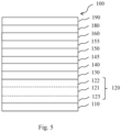
- the organic electronic device 100 includes a substrate 110, an anode layer 120, a hole injection layer (HIL) 130, a first hole transport layer (HTL1) 140, an electron blocking layer (EBL) 145, an emission layer (EML) 150, a hole blocking layer (HBL) 155, an electron transport layer (ETL) 160, an n-type charge generation layer (n-CGL) 185, a p-type charge generation layer (p-GCL) 135 which may comprise a compound of formula (I), a second hole transport layer (HTL2) 141, and electron injection layer (EIL) 180 and a cathode layer 190.
- the HIL may also comprise a compound of formula (I).
- the organic electronic device 100 includes a substrate 110, an anode layer 120, a hole injection layer (HIL) 130, a first hole transport layer (HTL) 140, a first electron blocking layer (EBL) 145, a first emission layer (EML) 150, an optional first hole blocking layer (HBL) 155, a first electron transport layer (ETL) 160, an n-type charge generation layer (n-CGL) 185, a p-type charge generation layer (p-GCL) 135 which may comprise compound of formula (I), a second hole transport layer (HTL) 141, a second electron blocking layer (EBL) 146, a second emission layer (EML) 151, an optional second hole blocking layer (HBL) 156, a second electron transport layer (ETL) 161, an electron injection layer (EIL) 180 and a cathode layer 190.
- the HIL may also comprise a compound of formula (I).
- a capping and/or sealing layer may further be formed on the cathode layer 190, in order to seal the organic electronic device 100.
- various other modifications may be applied thereto.
- the invention is furthermore illustrated by the following examples which are illustrative only and non-binding.
- the TGA5% value may be determined by heating a 9-11 mg sample in a thermogravimetric analyzer at a heating rate of 10 K/min in an open 100 ⁇ L aluminum pan, under a stream of nitrogen at a flow rate of 20 mL/min in the balance area and of 30 mL/min in the oven area.
- the TGA5% value may provide an indirect measure of the volatility and/or decomposition temperature of a compound. In first approximation, the higher the TGA5% value the lower is the volatility of a compound and/or the higher the decomposition temperature.
- the glass transition temperature (Tg) is measured under nitrogen and using a heating rate of 10 K per min in a Mettler Toledo DSC 822e differential scanning calorimeter as described in DIN EN ISO 11357, published in March 2010.
- the HOMO and LUMO are calculated with the program package TURBOMOLE V6.5 (TURBOMOLE GmbH, Litzenhardtstrasse 19, 76135 Düsseldorf, Germany).
- the optimized geometries and the HOMO and LUMO energy levels of the molecular structures are determined by applying the hybrid functional B3LYP with a 6-31G* basis set in the gas phase. If more than one conformation is viable, the conformation with the lowest total energy is selected.
- N-( ⁇ [1,1-'biphenyl]-4-yl)-9,9,dimethyl-N-(4-(9-phenyl-9H-carbazol-3-yl)phenyl)-9H-fluoren-2-amine ⁇ was vacuum deposited on the HIL, to form a HTL having a thickness of 121 nm.
- Yb was evaporated at a rate of 0.01 to 1 ⁇ /s at 10 -7 mbar to form an electron injection layer with a thickness of 2nm on the electron transporting layer.
- Ag/Mg (90:10 vol%) is evaporated at a rate of 0.01 to 1 ⁇ /s at 10 -7 mbar to form a cathode with a thickness of 13 nm.
- N-( ⁇ [1,1-'biphenyl]-4-yl)-9,9,dimethyl-N-(4-(9-phenyl-9H-carbazol-3-yl)phenyl)-9H-fluoren-2-amine ⁇ was vacuum deposited on the cathode layer to form a capping layer with a thickness of 75 nm.
- the OLED stack is protected from ambient conditions by encapsulation of the device with a glass slide. Thereby, a cavity is formed, which includes a getter material for further protection.
- the current efficiency is measured at 20°C.
- the current-voltage characteristic is determined using a Keithley 2635 source measure unit, by sourcing a voltage in V and measuring the current in mA flowing through the device under test. The voltage applied to the device is varied in steps of 0.1V in the range between 0V and 10V.
- the luminance-voltage characteristics and CIE coordinates are determined by measuring the luminance in cd/m 2 using an Instrument Systems CAS-140CT array spectrometer (calibrated by Deutsche Ak relie für sstelle (DAkkS)) for each of the voltage values.
- the cd/A efficiency at 10 mA/cm 2 is determined by interpolating the luminance-voltage and current-voltage characteristics, respectively.
- the efficiency EQE will be higher compared to bottom emission devices.
- the light output of the device is measured using a calibrated photodiode at 10 mA/cm 2 .
- Lifetime LT of the device is measured at ambient conditions (20°C) and 30 mA/cm 2 , using a Keithley 2400 sourcemeter, and recorded in hours.
- Table 1 and 2 are shown LUMO levels for inventive compounds xx to xx. LUMO levels were calculated with the program package TURBOMOLE V6.5 (TURBOMOLE GmbH, Litzenhardtstrasse 19, 76135 Düsseldorf, Germany) by applying the hybrid functional B3LYP with a 6-31G* basis set in the gas phase. Table 1: Calculated LUMO levels of compounds of formula (I) and comparative compounds.
- a lower operating voltage may be beneficial for improved battery life, in particular in mobile devices.
- a reduction of the increase in operating voltage over time may be beneficial for the lifetime, and improved stability of the electronic device.
- LT97 at 30 mA/cm2 is higher than for the comparative examples.
- a long lifetime may be beneficial for long-time stability of devices.
- the current efficiency (Ceff) may be higher than for the comparative example.
- a high efficiency may be beneficial for reduced power consumption and improved battery life, in particular in mobile devices.
Landscapes
- Chemical & Material Sciences (AREA)
- Organic Chemistry (AREA)
- Engineering & Computer Science (AREA)
- Materials Engineering (AREA)
- Physics & Mathematics (AREA)
- Spectroscopy & Molecular Physics (AREA)
- Optics & Photonics (AREA)
- Organic Low-Molecular-Weight Compounds And Preparation Thereof (AREA)
- Electroluminescent Light Sources (AREA)
Priority Applications (4)
| Application Number | Priority Date | Filing Date | Title |
|---|---|---|---|
| EP21198222.8A EP4155303A1 (fr) | 2021-09-22 | 2021-09-22 | Composé organique de formule (i) pour une utilisation dans des dispositifs électroniques organiques, composition comprenant un composé de formule (iv) et au moins un composé de formule (iva) à (ivd), couche semi-conductrice organique comprenant le composé ou la composition, dispositif électronique organique comprenant la couche semi-conductrice organique et dispositif d'affichage comprenant le dispositif électronique organique |
| PCT/EP2022/076210 WO2023046743A1 (fr) | 2021-09-22 | 2022-09-21 | Composé organique de formule (i) destiné à être utilisé dans des dispositifs électroniques organiques, composition comprenant un composé de formule (iv) et au moins un composé de formule (iva) à (ivd), couche semi-conductrice organique comprenant le composé ou la composition, dispositif électronique organique comprenant la couche semi-conductrice organique, et dispositif d'affichage comprenant le dispositif électronique organique |
| KR1020247012668A KR20240070583A (ko) | 2021-09-22 | 2022-09-21 | 유기 전자 장치에 사용하기 위한 화학식 (I)의 유기 화합물, 화학식 (IV)의 화합물 및 적어도 하나의 화학식 (Iva) 내지 (IVd)의 화합물을 포함하는 조성물, 상기 화합물 또는 조성물을 포함하는 유기 반도체층, 상기 유기 반도체층을 포함하는 유기 전자 장치 및 상기 유기 전자 장치를 포함하는 디스플레이 장치 |
| CN202280071180.5A CN118159531A (zh) | 2021-09-22 | 2022-09-21 | 用于有机电子器件中的式(I)的有机化合物、包含式(IV)的化合物和至少一种式(IVa)至(IVd)的化合物的组合物、包含该化合物或组合物的有机半导体层、包含该有机半导体层的有机电子器件以及包含该有机电子器件的显示装置 |
Applications Claiming Priority (1)
| Application Number | Priority Date | Filing Date | Title |
|---|---|---|---|
| EP21198222.8A EP4155303A1 (fr) | 2021-09-22 | 2021-09-22 | Composé organique de formule (i) pour une utilisation dans des dispositifs électroniques organiques, composition comprenant un composé de formule (iv) et au moins un composé de formule (iva) à (ivd), couche semi-conductrice organique comprenant le composé ou la composition, dispositif électronique organique comprenant la couche semi-conductrice organique et dispositif d'affichage comprenant le dispositif électronique organique |
Publications (1)
| Publication Number | Publication Date |
|---|---|
| EP4155303A1 true EP4155303A1 (fr) | 2023-03-29 |
Family
ID=77897561
Family Applications (1)
| Application Number | Title | Priority Date | Filing Date |
|---|---|---|---|
| EP21198222.8A Pending EP4155303A1 (fr) | 2021-09-22 | 2021-09-22 | Composé organique de formule (i) pour une utilisation dans des dispositifs électroniques organiques, composition comprenant un composé de formule (iv) et au moins un composé de formule (iva) à (ivd), couche semi-conductrice organique comprenant le composé ou la composition, dispositif électronique organique comprenant la couche semi-conductrice organique et dispositif d'affichage comprenant le dispositif électronique organique |
Country Status (4)
| Country | Link |
|---|---|
| EP (1) | EP4155303A1 (fr) |
| KR (1) | KR20240070583A (fr) |
| CN (1) | CN118159531A (fr) |
| WO (1) | WO2023046743A1 (fr) |
Citations (4)
| Publication number | Priority date | Publication date | Assignee | Title |
|---|---|---|---|---|
| EP2180029A1 (fr) | 2008-10-23 | 2010-04-28 | Novaled AG | Composés de Radialène et leur utilisation |
| EP2722908A1 (fr) | 2012-10-17 | 2014-04-23 | Novaled AG | Diode électroluminescente organique phosphorescente et matières de transport de trous pour diodes électroluminescentes phosphorescentes |
| WO2016097017A1 (fr) | 2014-12-16 | 2016-06-23 | Novaled Gmbh | 1,2,3-triylidènetris(cyanométhanylylidène)) cyclopropanes substitués pour vte, dispositifs électroniques et matériaux semi-conducteurs les utilisant |
| CN112624990A (zh) * | 2019-10-08 | 2021-04-09 | 广州华睿光电材料有限公司 | 含氮杂环取代的环丙烷类化合物及其应用 |
-
2021
- 2021-09-22 EP EP21198222.8A patent/EP4155303A1/fr active Pending
-
2022
- 2022-09-21 CN CN202280071180.5A patent/CN118159531A/zh active Pending
- 2022-09-21 WO PCT/EP2022/076210 patent/WO2023046743A1/fr active Application Filing
- 2022-09-21 KR KR1020247012668A patent/KR20240070583A/ko unknown
Patent Citations (4)
| Publication number | Priority date | Publication date | Assignee | Title |
|---|---|---|---|---|
| EP2180029A1 (fr) | 2008-10-23 | 2010-04-28 | Novaled AG | Composés de Radialène et leur utilisation |
| EP2722908A1 (fr) | 2012-10-17 | 2014-04-23 | Novaled AG | Diode électroluminescente organique phosphorescente et matières de transport de trous pour diodes électroluminescentes phosphorescentes |
| WO2016097017A1 (fr) | 2014-12-16 | 2016-06-23 | Novaled Gmbh | 1,2,3-triylidènetris(cyanométhanylylidène)) cyclopropanes substitués pour vte, dispositifs électroniques et matériaux semi-conducteurs les utilisant |
| CN112624990A (zh) * | 2019-10-08 | 2021-04-09 | 广州华睿光电材料有限公司 | 含氮杂环取代的环丙烷类化合物及其应用 |
Non-Patent Citations (1)
| Title |
|---|
| YASUHIKO SHIROTAHIROSHI KAGEYAMA, CHEM. REV., vol. 107, 2007, pages 953 - 1010 |
Also Published As
| Publication number | Publication date |
|---|---|
| CN118159531A (zh) | 2024-06-07 |
| KR20240070583A (ko) | 2024-05-21 |
| WO2023046743A1 (fr) | 2023-03-30 |
Similar Documents
| Publication | Publication Date | Title |
|---|---|---|
| EP3989305A1 (fr) | Dispositif électronique organique comprenant un composé de formule (1), dispositif d'affichage comprenant le dispositif électronique organique, ainsi que composés de formule (1) à utiliser dans des dispositifs électroniques organiques | |
| EP4284780A1 (fr) | Composé organique de formule (i) destiné à être utilisé dans des dispositifs électroniques organiques, dispositif électronique organique comprenant un composé de formule (i) et dispositif d'affichage comprenant le dispositif électronique organique | |
| WO2022101439A1 (fr) | Dispositif électronique organique comprenant un composé de formule (1), dispositif d'affichage comprenant le dispositif électronique organique et composés de formule (1) destinés à être utilisés dans des dispositifs électroniques organiques | |
| EP4169085B1 (fr) | Composé organique de formule (i) destiné à être utilisé dans des dispositifs électroniques organiques, dispositif électronique organique comprenant un composé de formule (i) et dispositif d'affichage comprenant le dispositif électronique organique | |
| EP3930024B1 (fr) | Dispositif électronique organique et dispositif d'affichage comprenant le dispositif électronique organique ainsi qu'une composition destinée à être utilisée dans des dispositifs électroniques organiques | |
| EP3930022A1 (fr) | Dispositif électronique organique et dispositif d'affichage comprenant le dispositif électronique organique ainsi qu'une composition destinée à être utilisée dans des dispositifs électroniques organiques | |
| EP4155303A1 (fr) | Composé organique de formule (i) pour une utilisation dans des dispositifs électroniques organiques, composition comprenant un composé de formule (iv) et au moins un composé de formule (iva) à (ivd), couche semi-conductrice organique comprenant le composé ou la composition, dispositif électronique organique comprenant la couche semi-conductrice organique et dispositif d'affichage comprenant le dispositif électronique organique | |
| EP3989303A1 (fr) | Composé organique de formule (i) à utiliser dans des dispositifs électroniques organiques, dispositif électronique organique comprenant un composé de formule (i) et dispositif d'affichage comprenant le dispositif électronique organique | |
| EP4106034A1 (fr) | Dispositif électronique organique comprenant un composé métallique comportant des cations métalliques et au moins un anion de borate de formule (i), dispositif d'affichage comprenant le dispositif électronique organique, utilisation du composé métallique dans un dispositif électronique organique et procédé de préparation du dispositif électronique organique | |
| EP3989304A1 (fr) | Composé organique de formule (i) pour une utilisation dans des dispositifs électroniques organiques, dispositif électronique organique comprenant un composé de formule (i) et dispositif d'affichage comprenant le dispositif électronique organique | |
| EP3989302A1 (fr) | Composé organique de formule (i) pour une utilisation dans des dispositifs électroniques organiques, dispositif électronique organique comprenant un composé de formule (i) et dispositif d'affichage comprenant le dispositif électronique organique | |
| EP3989301A1 (fr) | Dispositif électronique organique comprenant un composé de formule (1), dispositif d'affichage comprenant le dispositif électronique organique, ainsi que composés de formule (1) à utiliser dans des dispositifs électroniques organiques | |
| EP3930023A1 (fr) | Dispositif électronique organique comprenant un composé de formule (1), dispositif d'affichage comprenant le dispositif électronique organique, ainsi que composés de formule (1) à utiliser dans des dispositifs électroniques organiques |
Legal Events
| Date | Code | Title | Description |
|---|---|---|---|
| PUAI | Public reference made under article 153(3) epc to a published international application that has entered the european phase |
Free format text: ORIGINAL CODE: 0009012 |
|
| STAA | Information on the status of an ep patent application or granted ep patent |
Free format text: STATUS: THE APPLICATION HAS BEEN PUBLISHED |
|
| AK | Designated contracting states |
Kind code of ref document: A1 Designated state(s): AL AT BE BG CH CY CZ DE DK EE ES FI FR GB GR HR HU IE IS IT LI LT LU LV MC MK MT NL NO PL PT RO RS SE SI SK SM TR |
|
| STAA | Information on the status of an ep patent application or granted ep patent |
Free format text: STATUS: REQUEST FOR EXAMINATION WAS MADE |
|
| 17P | Request for examination filed |
Effective date: 20230913 |
|
| RBV | Designated contracting states (corrected) |
Designated state(s): AL AT BE BG CH CY CZ DE DK EE ES FI FR GB GR HR HU IE IS IT LI LT LU LV MC MK MT NL NO PL PT RO RS SE SI SK SM TR |