EP4152909A1 - Spatially controlled conductivity in transparent oxide coatings - Google Patents
Spatially controlled conductivity in transparent oxide coatings Download PDFInfo
- Publication number
- EP4152909A1 EP4152909A1 EP22182912.0A EP22182912A EP4152909A1 EP 4152909 A1 EP4152909 A1 EP 4152909A1 EP 22182912 A EP22182912 A EP 22182912A EP 4152909 A1 EP4152909 A1 EP 4152909A1
- Authority
- EP
- European Patent Office
- Prior art keywords
- semiconductor
- semiconductor coating
- coating
- photoresist
- recited
- Prior art date
- Legal status (The legal status is an assumption and is not a legal conclusion. Google has not performed a legal analysis and makes no representation as to the accuracy of the status listed.)
- Pending
Links
Images


Classifications
-
- G—PHYSICS
- G02—OPTICS
- G02B—OPTICAL ELEMENTS, SYSTEMS OR APPARATUS
- G02B1/00—Optical elements characterised by the material of which they are made; Optical coatings for optical elements
- G02B1/10—Optical coatings produced by application to, or surface treatment of, optical elements
- G02B1/16—Optical coatings produced by application to, or surface treatment of, optical elements having an anti-static effect, e.g. electrically conducting coatings
-
- C—CHEMISTRY; METALLURGY
- C23—COATING METALLIC MATERIAL; COATING MATERIAL WITH METALLIC MATERIAL; CHEMICAL SURFACE TREATMENT; DIFFUSION TREATMENT OF METALLIC MATERIAL; COATING BY VACUUM EVAPORATION, BY SPUTTERING, BY ION IMPLANTATION OR BY CHEMICAL VAPOUR DEPOSITION, IN GENERAL; INHIBITING CORROSION OF METALLIC MATERIAL OR INCRUSTATION IN GENERAL
- C23C—COATING METALLIC MATERIAL; COATING MATERIAL WITH METALLIC MATERIAL; SURFACE TREATMENT OF METALLIC MATERIAL BY DIFFUSION INTO THE SURFACE, BY CHEMICAL CONVERSION OR SUBSTITUTION; COATING BY VACUUM EVAPORATION, BY SPUTTERING, BY ION IMPLANTATION OR BY CHEMICAL VAPOUR DEPOSITION, IN GENERAL
- C23C14/00—Coating by vacuum evaporation, by sputtering or by ion implantation of the coating forming material
- C23C14/04—Coating on selected surface areas, e.g. using masks
- C23C14/042—Coating on selected surface areas, e.g. using masks using masks
-
- C—CHEMISTRY; METALLURGY
- C23—COATING METALLIC MATERIAL; COATING MATERIAL WITH METALLIC MATERIAL; CHEMICAL SURFACE TREATMENT; DIFFUSION TREATMENT OF METALLIC MATERIAL; COATING BY VACUUM EVAPORATION, BY SPUTTERING, BY ION IMPLANTATION OR BY CHEMICAL VAPOUR DEPOSITION, IN GENERAL; INHIBITING CORROSION OF METALLIC MATERIAL OR INCRUSTATION IN GENERAL
- C23C—COATING METALLIC MATERIAL; COATING MATERIAL WITH METALLIC MATERIAL; SURFACE TREATMENT OF METALLIC MATERIAL BY DIFFUSION INTO THE SURFACE, BY CHEMICAL CONVERSION OR SUBSTITUTION; COATING BY VACUUM EVAPORATION, BY SPUTTERING, BY ION IMPLANTATION OR BY CHEMICAL VAPOUR DEPOSITION, IN GENERAL
- C23C14/00—Coating by vacuum evaporation, by sputtering or by ion implantation of the coating forming material
- C23C14/06—Coating by vacuum evaporation, by sputtering or by ion implantation of the coating forming material characterised by the coating material
- C23C14/08—Oxides
- C23C14/086—Oxides of zinc, germanium, cadmium, indium, tin, thallium or bismuth
-
- C—CHEMISTRY; METALLURGY
- C23—COATING METALLIC MATERIAL; COATING MATERIAL WITH METALLIC MATERIAL; CHEMICAL SURFACE TREATMENT; DIFFUSION TREATMENT OF METALLIC MATERIAL; COATING BY VACUUM EVAPORATION, BY SPUTTERING, BY ION IMPLANTATION OR BY CHEMICAL VAPOUR DEPOSITION, IN GENERAL; INHIBITING CORROSION OF METALLIC MATERIAL OR INCRUSTATION IN GENERAL
- C23C—COATING METALLIC MATERIAL; COATING MATERIAL WITH METALLIC MATERIAL; SURFACE TREATMENT OF METALLIC MATERIAL BY DIFFUSION INTO THE SURFACE, BY CHEMICAL CONVERSION OR SUBSTITUTION; COATING BY VACUUM EVAPORATION, BY SPUTTERING, BY ION IMPLANTATION OR BY CHEMICAL VAPOUR DEPOSITION, IN GENERAL
- C23C14/00—Coating by vacuum evaporation, by sputtering or by ion implantation of the coating forming material
- C23C14/22—Coating by vacuum evaporation, by sputtering or by ion implantation of the coating forming material characterised by the process of coating
- C23C14/48—Ion implantation
-
- C—CHEMISTRY; METALLURGY
- C23—COATING METALLIC MATERIAL; COATING MATERIAL WITH METALLIC MATERIAL; CHEMICAL SURFACE TREATMENT; DIFFUSION TREATMENT OF METALLIC MATERIAL; COATING BY VACUUM EVAPORATION, BY SPUTTERING, BY ION IMPLANTATION OR BY CHEMICAL VAPOUR DEPOSITION, IN GENERAL; INHIBITING CORROSION OF METALLIC MATERIAL OR INCRUSTATION IN GENERAL
- C23C—COATING METALLIC MATERIAL; COATING MATERIAL WITH METALLIC MATERIAL; SURFACE TREATMENT OF METALLIC MATERIAL BY DIFFUSION INTO THE SURFACE, BY CHEMICAL CONVERSION OR SUBSTITUTION; COATING BY VACUUM EVAPORATION, BY SPUTTERING, BY ION IMPLANTATION OR BY CHEMICAL VAPOUR DEPOSITION, IN GENERAL
- C23C14/00—Coating by vacuum evaporation, by sputtering or by ion implantation of the coating forming material
- C23C14/58—After-treatment
- C23C14/5806—Thermal treatment
-
- G—PHYSICS
- G02—OPTICS
- G02B—OPTICAL ELEMENTS, SYSTEMS OR APPARATUS
- G02B1/00—Optical elements characterised by the material of which they are made; Optical coatings for optical elements
- G02B1/02—Optical elements characterised by the material of which they are made; Optical coatings for optical elements made of crystals, e.g. rock-salt, semi-conductors
-
- H—ELECTRICITY
- H05—ELECTRIC TECHNIQUES NOT OTHERWISE PROVIDED FOR
- H05K—PRINTED CIRCUITS; CASINGS OR CONSTRUCTIONAL DETAILS OF ELECTRIC APPARATUS; MANUFACTURE OF ASSEMBLAGES OF ELECTRICAL COMPONENTS
- H05K9/00—Screening of apparatus or components against electric or magnetic fields
- H05K9/0073—Shielding materials
- H05K9/0094—Shielding materials being light-transmitting, e.g. transparent, translucent
-
- H—ELECTRICITY
- H10—SEMICONDUCTOR DEVICES; ELECTRIC SOLID-STATE DEVICES NOT OTHERWISE PROVIDED FOR
- H10P—GENERIC PROCESSES OR APPARATUS FOR THE MANUFACTURE OR TREATMENT OF DEVICES COVERED BY CLASS H10
- H10P14/00—Formation of materials, e.g. in the shape of layers or pillars
- H10P14/20—Formation of materials, e.g. in the shape of layers or pillars of semiconductor materials
- H10P14/34—Deposited materials, e.g. layers
- H10P14/3402—Deposited materials, e.g. layers characterised by the chemical composition
- H10P14/3434—Deposited materials, e.g. layers characterised by the chemical composition being oxide semiconductor materials
-
- H—ELECTRICITY
- H10—SEMICONDUCTOR DEVICES; ELECTRIC SOLID-STATE DEVICES NOT OTHERWISE PROVIDED FOR
- H10P—GENERIC PROCESSES OR APPARATUS FOR THE MANUFACTURE OR TREATMENT OF DEVICES COVERED BY CLASS H10
- H10P14/00—Formation of materials, e.g. in the shape of layers or pillars
- H10P14/20—Formation of materials, e.g. in the shape of layers or pillars of semiconductor materials
- H10P14/38—Formation of materials, e.g. in the shape of layers or pillars of semiconductor materials characterised by treatments done after the formation of the materials
-
- C—CHEMISTRY; METALLURGY
- C23—COATING METALLIC MATERIAL; COATING MATERIAL WITH METALLIC MATERIAL; CHEMICAL SURFACE TREATMENT; DIFFUSION TREATMENT OF METALLIC MATERIAL; COATING BY VACUUM EVAPORATION, BY SPUTTERING, BY ION IMPLANTATION OR BY CHEMICAL VAPOUR DEPOSITION, IN GENERAL; INHIBITING CORROSION OF METALLIC MATERIAL OR INCRUSTATION IN GENERAL
- C23C—COATING METALLIC MATERIAL; COATING MATERIAL WITH METALLIC MATERIAL; SURFACE TREATMENT OF METALLIC MATERIAL BY DIFFUSION INTO THE SURFACE, BY CHEMICAL CONVERSION OR SUBSTITUTION; COATING BY VACUUM EVAPORATION, BY SPUTTERING, BY ION IMPLANTATION OR BY CHEMICAL VAPOUR DEPOSITION, IN GENERAL
- C23C16/00—Chemical coating by decomposition of gaseous compounds, without leaving reaction products of surface material in the coating, i.e. chemical vapour deposition [CVD] processes
- C23C16/22—Chemical coating by decomposition of gaseous compounds, without leaving reaction products of surface material in the coating, i.e. chemical vapour deposition [CVD] processes characterised by the deposition of inorganic material, other than metallic material
- C23C16/30—Deposition of compounds, mixtures or solid solutions, e.g. borides, carbides, nitrides
- C23C16/308—Oxynitrides
Definitions
- the present disclosure relates to optical coatings, and more particularly to electrically conductive optical coatings.
- Electro-optic (EO) systems require windows to protect the sensor and electronics from outside elements. In addition to rain, dust, and the like, in many cases the window must also block electromagnetic interference (EMI) that would otherwise impede the EO system performance.
- EMI electromagnetic interference
- EMI shielding can be accomplished with a window that is electrically conductive and optically transparent. There are three conventional types of shielding.
- the first type of EMI shielded window uses a semiconductor material such as silicon or germanium that is doped with a group V element such as phosphorous, arsine, or antimony to supply additional electrons to provide electrical conductivity. These windows are opaque for visible wavelengths and are thus not useful for broadband EO systems.
- the second type of shielded window uses a continuous, transparent, conductive coating.
- These coatings consist of wide bandgap semiconductors such as indium oxide (In 2 O 3 ) and zinc oxide (ZnO) that have broadband optical transparency.
- the semiconductors are doped to provide electrical conductivity.
- optical transmittance decreases. This effect begins at longer wavelengths where both plasma reflectance and free-carrier absorption from electrons decrease transmittance.
- Traditional transparent, conductive semiconductor coatings are practical only in the 0.4 to 2.0 micron range, short wavelength visible through short wavelength infrared, (SWIR).
- the third type of shielded window is traditionally required for broadband applications from the visible to the long-wave infrared (LWIR).
- LWIR long-wave infrared
- a grid of fine metal lines is applied on the surface of the window. Typical dimensions are 5-micron wide lines with 140 micron spacing.
- U.S. Patent No. 9,276,034 presents a method for reducing the optical scattering from a conductive grid.
- Channels are etched into a window substrate, and an electrically conductive semiconductor is deposited in the channels such that the surface of the window is planar.
- the semiconductor is transparent for visible and short wavelength infrared (SWIR) wavelengths but reflecting and absorbing for mid wavelength infrared (MWIR) and longer wavelengths.
- SWIR visible and short wavelength infrared
- MWIR mid wavelength infrared
- a method of coating an optical substrate includes depositing a semiconductor coating (e.g. a coating as described herein) over a surface of an optical substrate, wherein the semiconductor coating has broadband optical transmittance. Portions of the semiconductor coating are doped to form a spatially varied pattern of doped semiconductor in the semiconductor coating.
- the method includes annealing the semiconductor coating, e.g. to do at least one of: increase oxygen in undoped areas of the semiconductor coating; or reduce oxygen in doped areas of the semiconductor coating.
- Annealing the semiconductor coating can include laser annealing in a predetermined pattern, e.g. to improve the crystal quality of transparent conducting oxide (TCO) materials of the semiconductor coating and increase electrical conductivity in doped areas of the semiconductor coating.
- TCO transparent conducting oxide
- Annealing the semiconductor coating can include annealing in air, e.g. to activate and diffuse dopant and increase oxygen in undoped areas of the semiconductor coating.
- Doping portions of the semiconductor coating can include:
- annealing the semiconductor coating can include annealing under vacuum to activate and diffuse dopant and reduce oxygen in doped areas of the semiconductor coating.
- Doping portions of the semiconductor coating can include:
- the semiconductor coating can include at least one of In 2 O 3 or ZnO. Doping portions of the semiconductor coating to form a spatially varied pattern can include applying dopant by ion implantation, a spin-on or spray-on dopant solution, or other methods.
- the doped semiconductor can include at least one of Sn, Mo, W, Ti, Al, or Ga.
- the semiconductor coating can have broadband optical transmittance in at least visible and infrared spectra.
- Depositing the semiconductor coating can include depositing the semiconductor coating with the semiconductor coating undoped. Doping portions of the semiconductor coating and annealing the semiconductor coating can include diffusing the dopant atoms through the semiconductor coating to the optical substrate.
- Depositing a semiconductor coating can include depositing the semiconductor coating over a surface of the optical substrate in its entirety.
- Doping portions of the semiconductor coating to form a spatially varied pattern can include doping a surface of the semiconductor coating so a surface of the semiconductor coating is covered in its entirety with the pattern.
- the semiconductor coating including annealed activated doped semiconductor in the semiconductor coating and the optical substrate can be formed into a window without etching and/or without polishing or post-process planarization.
- the activated doped semiconductor and the semiconductor coating can have closely matched indices of refraction to mitigate light scattering (e.g. from the pattern). If the ratio of the indices of refraction of the doped semiconductor and semiconductor coating is between 0.82 and 1.22, the interface reflection will be less than 1% at normal incidence.
- the indices of refraction of doped and undoped In 2 O 3 at 632.8 nm are about 2.00 and 1.77, respectively.
- the index ratio of 1.13 produces a reflection of only 0.37%.
- the method can include making the doped semiconductor electrically conductive. Hydrogen can be added to the doped semiconductor (e.g. to increase conductivity by adding electrons and passivating defects), such as by a plasma-enhanced chemical vapor deposition (PECVD) silicon oxynitride process or use of a hydrogen plasma.
- PECVD plasma-enhanced chemical vapor deposition
- a window (e.g. formed by the methods as described herein) includes a transparent substrate (e.g. an optical substrate as described herein) with a coating over the transparent substrate, the coating being made of both a transparent semiconductor and an electrically conductive semiconductor with lower transparency than the transparent semiconductor (e.g. by the method disclosed herein), the electrically conductive semiconductor being annealed and distributed in a spatially varied pattern in the transparent semiconductor.
- the electrically conductive semiconductor may be laser annealed.
- the transparent semiconductor may include a transparent conducting oxide (TCO) material.
- the electrically conductive semiconductor may include a semiconductor material doped for electrical conductivity.
- the doped semiconductor may include at least one of Sn, Mo, W, Ti, Al, or Ga.
- Fig. 1 a partial view of an exemplary embodiment of a window or optic in accordance with the disclosure is shown in Fig. 1 and is designated generally by reference character 100.
- the systems and methods described herein can be used to provide spatially controlled or varied electrical conductivity in transparent oxide coatings for optics and windows. This can be used for electromagnetic interference (EMI) shielding, spatially varying sheet resistance for smart window applications, or any other suitable application.
- EMI electromagnetic interference
- Transparent, conductive oxides such as indium tin oxide (ITO) and aluminum zinc oxide (AZO) are important coating materials for a wide variety of products that require optical transparency and electrical conductivity.
- ITO indium tin oxide
- AZO aluminum zinc oxide
- the indium oxide (In 2 O 3 ) and zinc oxide (ZnO) wide bandgap semiconductors have broadband optical transparency.
- the materials can be doped to provide electrical conductivity. However, as doping rises to increase electrical conductivity, optical transmittance decreases. This effect begins at longer wavelengths where both plasma reflectance and free-carrier absorption from electrons decrease transmittance.
- the common conductive oxide coatings are generally transparent only in the 0.4 to 2.0 micron wavelength range. This disclosure explains methods to spatially control the conductivity and transmittance of a transparent oxide thin film in different areas of a coating.
- a method of coating an optical substrate 102 includes depositing a semiconductor coating 104 over a surface of an optical substrate 102, e.g. over the entire surface of the optical substrate 102.
- Depositing the semiconductor coating 104 can include depositing the semiconductor coating 104 with the semiconductor coating 104 undoped, and in the presence of oxygen.
- oxide semiconductors can be annealed in air to provide excess oxygen in the semiconductor coating 104.
- the semiconductor coating 104 has broadband optical transmittance as a transparent conducting oxide (TCO) material, and can include In 2 O 3 , ZnO, or the like, e.g., wherein the electrical sheet resistance is greater than 2000 ohms/square.
- TCO transparent conducting oxide
- the semiconductor coating can therefore have broadband optical transmittance in at least visible and infrared spectra.
- Portions of the semiconductor coating 104 are doped to form a spatially varied pattern of doped semiconductor in the semiconductor coating as described further below. Doping portions of the semiconductor coating to form a spatially varied pattern can include applying dopant by ion implantation of donor atoms. Any other suitable technique can be used without departing from the scope of this disclosure, such as spin-on or spray-on dopant solutions.
- the doped semiconductor can include at least one of Sn, Mo, W, Ti, Al, or Ga. Hydrogen can serve as an electron donor and can passivate defects.
- the method includes annealing the semiconductor coating 104 to diffuse the dopant atoms through the semiconductor coating and to do at least one of: increase oxygen in undoped areas of the semiconductor coating; or reduce oxygen in doped areas of the semiconductor coating.
- annealing the semiconductor coating 104 can include thermal annealing and/or laser annealing in a predetermined pattern to improve crystal quality of the TCO materials of the semiconductor coating 104 and increase electrical conductivity in doped areas of the semiconductor coating 104.
- Annealing the semiconductor coating 104 can include annealing in air to activate and diffuse dopant and increase oxygen in undoped areas of the semiconductor coating 104.
- Doping portions of the semiconductor coating can include applying a photoresist 106 over the semiconductor coating as shown in Fig. 2 . The photoresist is selectively exposed and developed in the predetermined, spatially varied pattern, i.e., any pattern can be used, but in Fig.
- spatial variation in the pattern includes a wider opening in photoresist 106 on the left than on the right opening in the photoresist 106.
- the method includes doping the semiconductor coating 104 through the openings 105 in the photoresist 106, as indicated by the downward arrows shown in Fig. 3 .
- the photoresist 106 is removed, e.g., using a solvent, to leave the doped semiconductor 108 in the pattern in the semiconductor coating 104.
- a coating of silicon oxynitride 110 is applied using plasma-enhanced chemical vapor deposition (PECVD) or the like over the entire surface of the semiconductor coating 104, as shown in Fig. 5 .
- PECVD plasma-enhanced chemical vapor deposition
- Hydrogen in the PECVD process increases conductivity by adding electrons and passivating defects in oxide semiconductors.
- a hydrogen plasma can also be used.
- silicon oxynitride is used as an example herein, those skilled in the art will readily appreciate that any other suitable protective film can be used without departing from the scope of this disclosure.
- Another photoresist 112 is applied over the silicon oxynitride 110, as shown in Fig. 6 . This photoresist 112 is exposed and developed in the inverse pattern of the first photoresist 106, and portions of the silicon oxynitride not covered by photoresist are removed as shown in Fig. 7 , e.g., using diluted hydrofluoric acid (HF:H 2 O).
- the remaining photoresist 112 is removed as shown in in Fig. 8 , to prepare the substrate for annealing.
- the method includes annealing the semiconductor coating 104, including annealing the silicon oxynitride 110 and semiconductor coating 104 in air, as indicated in Fig. 9 , to activate and diffuse dopant and increase oxygen in undoped areas of the semiconductor coating 104.
- the sheet resistance of undoped In 2 O 3 can be increased from ⁇ 100 ohms/square to >2000 ohms/square by increasing oxygen with air annealing.
- the remaining portions of silicon oxynitride 110 can then be removed from the substrate as shown in Fig. 10 , where the activated, annealed dopant in doped areas 108 forms the predetermined, electrically conductive pattern in semiconductor coating 104.
- Doping portions 108 of the semiconductor coating 104 and annealing the semiconductor coating 104 can include diffusing the doped semiconductor through the semiconductor coating 104 to the optical substrate 102, i.e. the dopant diffuses all the way through the thickness of the semiconductor coating 104, as shown in Fig. 10 .
- the top surface of the semiconductor coating 104 can be covered in its entirety with the pattern, which can be varied spatially to achieve any desired electrical conductivity as a function of two-dimensional location on the window or optic 100.
- the optic or window 100 can thus be formed into a window having an electrically conductive coating, with broadband transparency, without etching and/or without polishing or post-process planarization.
- the activated doped semiconductor portions 108 and the semiconductor coating 104 can have closely matched indices of refraction to mitigate light scattering from the pattern. If the ratio of the indices of refraction of the doped semiconductor and semiconductor coating is between 0.82 and 1.22, the interface reflection will be less than 1% at normal incidence. For example, the indices of refraction of doped and undoped In 2 O 3 at 632.8 nm are about 2.00 and 1.77, respectively. The index ratio of 1.13 produces a reflection of only 0.37%.
- the resulting window or optic 100 shown in Fig. 10 includes a transparent substrate, i.e. optical substrate 102, with a coating over the transparent substrate, the coating being made of both a transparent semiconductor and an electrically conductive semiconductor, i.e., a semiconductor coating 104 with electrically conductive portions 108.
- a coating of silicon oxynitride 110 is applied over the entire surface of the semiconductor coating 104 with the semiconductor undoped.
- a photoresist 106 is applied over the silicon oxynitride 110, as shown in Fig. 12 , and the photoresist 106 is exposed and developed.
- the developed photoresist 106 protects portions of the silicon oxynitride 110, and the unprotected portions of silicon oxynitride 110 are removed to expose portions 108 of the semiconductor coating 104 as shown in Fig. 13 .
- the semiconductor coating 104 is doped through openings 105 in the photoresist 106.
- the photoresist 106 could be removed before doping, otherwise, the photoresist 106 is removed after doping as shown in Fig. 14 to leave the doped semiconductor portions 108 in the pattern in the semiconductor coating 104.
- Annealing the silicon oxynitride 110 and semiconductor coating 104 under vacuum, as indicated in Fig. 15 activates and diffuses the dopant and reduces oxygen in doped areas, i.e. portions 108, of the semiconductor coating 104. Oxygen vacancies contribute electrons and increase conductivity in oxide semiconductors.
- the sheet resistance of In 2 O 3 can be reduced from >2000 ohms/square to ⁇ 100 ohms/square by reducing oxygen with vacuum annealing.
- the silicon oxynitride 110 can then be removed to arrive at the structure shown in Fig. 10 .
- This disclosure relates to transparent conductive oxides (TCO) or oxide semiconductors where there is an increase or decrease of oxygen in selected areas during an annealing process. These oxygen changes decrease or increase the electron concentration and conductivity of the semiconductor, respectively.
- the sheet resistance of undoped In203 can be changed from >2000 ohms/square to ⁇ 100 ohms/square and vice-versa by decreasing and increasing oxygen, respectively.
Landscapes
- Chemical & Material Sciences (AREA)
- Engineering & Computer Science (AREA)
- Physics & Mathematics (AREA)
- Materials Engineering (AREA)
- Organic Chemistry (AREA)
- Metallurgy (AREA)
- Mechanical Engineering (AREA)
- Chemical Kinetics & Catalysis (AREA)
- General Physics & Mathematics (AREA)
- Optics & Photonics (AREA)
- Crystallography & Structural Chemistry (AREA)
- Microelectronics & Electronic Packaging (AREA)
- Thermal Sciences (AREA)
- Surface Treatment Of Optical Elements (AREA)
- Surface Treatment Of Glass (AREA)
- Manufacturing Of Electric Cables (AREA)
- Plasma & Fusion (AREA)
- General Chemical & Material Sciences (AREA)
- Physical Vapour Deposition (AREA)
- Thin Film Transistor (AREA)
- Optical Modulation, Optical Deflection, Nonlinear Optics, Optical Demodulation, Optical Logic Elements (AREA)
Abstract
Description
- The present disclosure relates to optical coatings, and more particularly to electrically conductive optical coatings.
- Electro-optic (EO) systems require windows to protect the sensor and electronics from outside elements. In addition to rain, dust, and the like, in many cases the window must also block electromagnetic interference (EMI) that would otherwise impede the EO system performance.
- EMI shielding can be accomplished with a window that is electrically conductive and optically transparent. There are three conventional types of shielding.
- The first type of EMI shielded window uses a semiconductor material such as silicon or germanium that is doped with a group V element such as phosphorous, arsine, or antimony to supply additional electrons to provide electrical conductivity. These windows are opaque for visible wavelengths and are thus not useful for broadband EO systems.
- The second type of shielded window uses a continuous, transparent, conductive coating. These coatings consist of wide bandgap semiconductors such as indium oxide (In2O3) and zinc oxide (ZnO) that have broadband optical transparency. The semiconductors are doped to provide electrical conductivity. However, as doping increases to increase electrical conductivity and EMI attenuation, optical transmittance decreases. This effect begins at longer wavelengths where both plasma reflectance and free-carrier absorption from electrons decrease transmittance. Traditional transparent, conductive semiconductor coatings are practical only in the 0.4 to 2.0 micron range, short wavelength visible through short wavelength infrared, (SWIR).
- The third type of shielded window is traditionally required for broadband applications from the visible to the long-wave infrared (LWIR). A grid of fine metal lines is applied on the surface of the window. Typical dimensions are 5-micron wide lines with 140 micron spacing. These gridded windows enable optical transmittance over a broad wavelength range, but they limit optical transmittance by obscuration and scattering.
-
U.S. Patent No. 9,276,034 - The conventional techniques have been considered satisfactory for their intended purpose. However, there is an ever present need for improved electrically conductive optical coatings, e.g., for broad band optics. This disclosure provides a solution for this problem.
- A method of coating an optical substrate (e.g. to form a window as herein described) includes depositing a semiconductor coating (e.g. a coating as described herein) over a surface of an optical substrate, wherein the semiconductor coating has broadband optical transmittance. Portions of the semiconductor coating are doped to form a spatially varied pattern of doped semiconductor in the semiconductor coating. The method includes annealing the semiconductor coating, e.g. to do at least one of: increase oxygen in undoped areas of the semiconductor coating; or reduce oxygen in doped areas of the semiconductor coating.
- Annealing the semiconductor coating can include laser annealing in a predetermined pattern, e.g. to improve the crystal quality of transparent conducting oxide (TCO) materials of the semiconductor coating and increase electrical conductivity in doped areas of the semiconductor coating.
- Annealing the semiconductor coating can include annealing in air, e.g. to activate and diffuse dopant and increase oxygen in undoped areas of the semiconductor coating. Doping portions of the semiconductor coating can include:
- applying a photoresist over the semiconductor coating;
- selectively exposing the photoresist;
- developing the photoresist in the pattern;
- doping the semiconductor coating through openings in the photoresist;
- removing the photoresist to leave the doped semiconductor in the pattern on the semiconductor coating;
- applying a coating of silicon oxynitride over the entire surface of the semiconductor coating;
- applying a photoresist over the silicon oxynitride, exposing the photoresist, and developing the photoresist;
- removing portions of the silicon oxynitride not covered by photoresist and then removing any remaining photoresist; and
- wherein annealing the semiconductor coating includes annealing the silicon oxynitride and semiconductor coating in air to activate and diffuse dopant and increase oxygen in undoped areas of the semiconductor coating.
- It is also contemplated that annealing the semiconductor coating can include annealing under vacuum to activate and diffuse dopant and reduce oxygen in doped areas of the semiconductor coating. Doping portions of the semiconductor coating can include:
- applying a coating of silicon oxynitride over the entire surface of the semiconductor coating with the semiconductor undoped;
- applying a photoresist over the silicon oxynitride, exposing the photoresist, and developing the photoresist;
- removing portions of the silicon oxynitride not covered by photoresist;
- doping the semiconductor coating through openings in the photoresist;
- removing the photoresist to leave the doped semiconductor in the pattern on the semiconductor coating; and
- wherein annealing the semiconductor coating includes annealing the silicon oxynitride and semiconductor coating in vacuum to activate and diffuse dopant and reduce oxygen in doped areas of the semiconductor coating.
- The semiconductor coating can include at least one of In2O3 or ZnO. Doping portions of the semiconductor coating to form a spatially varied pattern can include applying dopant by ion implantation, a spin-on or spray-on dopant solution, or other methods. The doped semiconductor can include at least one of Sn, Mo, W, Ti, Al, or Ga. The semiconductor coating can have broadband optical transmittance in at least visible and infrared spectra. Depositing the semiconductor coating can include depositing the semiconductor coating with the semiconductor coating undoped. Doping portions of the semiconductor coating and annealing the semiconductor coating can include diffusing the dopant atoms through the semiconductor coating to the optical substrate. Depositing a semiconductor coating can include depositing the semiconductor coating over a surface of the optical substrate in its entirety. Doping portions of the semiconductor coating to form a spatially varied pattern can include doping a surface of the semiconductor coating so a surface of the semiconductor coating is covered in its entirety with the pattern. The semiconductor coating including annealed activated doped semiconductor in the semiconductor coating and the optical substrate can be formed into a window without etching and/or without polishing or post-process planarization. The activated doped semiconductor and the semiconductor coating can have closely matched indices of refraction to mitigate light scattering (e.g. from the pattern). If the ratio of the indices of refraction of the doped semiconductor and semiconductor coating is between 0.82 and 1.22, the interface reflection will be less than 1% at normal incidence. For example, the indices of refraction of doped and undoped In2O3 at 632.8 nm are about 2.00 and 1.77, respectively. The index ratio of 1.13 produces a reflection of only 0.37%. The method can include making the doped semiconductor electrically conductive. Hydrogen can be added to the doped semiconductor (e.g. to increase conductivity by adding electrons and passivating defects), such as by a plasma-enhanced chemical vapor deposition (PECVD) silicon oxynitride process or use of a hydrogen plasma.
- A window (e.g. formed by the methods as described herein) includes a transparent substrate (e.g. an optical substrate as described herein) with a coating over the transparent substrate, the coating being made of both a transparent semiconductor and an electrically conductive semiconductor with lower transparency than the transparent semiconductor (e.g. by the method disclosed herein), the electrically conductive semiconductor being annealed and distributed in a spatially varied pattern in the transparent semiconductor. The electrically conductive semiconductor may be laser annealed. The transparent semiconductor may include a transparent conducting oxide (TCO) material. The electrically conductive semiconductor may include a semiconductor material doped for electrical conductivity. The doped semiconductor may include at least one of Sn, Mo, W, Ti, Al, or Ga.
- These and other features of the systems and methods of the subject disclosure will become more readily apparent to those skilled in the art from the following detailed description of the preferred embodiments taken in conjunction with the drawings.
- So that those skilled in the art to which the subject disclosure appertains will readily understand how to make and use the devices and methods of the subject disclosure without undue experimentation, preferred embodiments thereof will be described in detail herein below with reference to certain figures, wherein:
-
Fig. 1 is a schematic cross-sectional elevation view of an exemplary embodiment of a window or optic constructed in accordance with the present disclosure, showing a semiconductor coating on an optical substrate; -
Fig. 2 is a schematic cross-sectional elevation view of the window or optic ofFig. 1 , showing a layer of photoresist deposited on the semiconductor coating; -
Fig. 3 is a schematic cross-sectional elevation view of the window or optic ofFig. 2 , showing a portion of the developed photoresist removed to allow doping of the semiconductor coating in a predetermined spatially varied pattern; -
Fig. 4 is a schematic cross-sectional elevation view of the window or optic ofFig. 3 , showing the photoresist removed and a doped pattern in the semiconductor coating; -
Fig. 5 is a schematic cross-sectional elevation view of the window or optic ofFig. 4 , showing a layer of silicon oxynitride deposited on the semiconductor coating; -
Fig. 6 is a schematic cross-sectional elevation view of the window or optic ofFig. 5 , showing a layer of photoresist deposited on the silicon oxynitride; -
Fig. 7 is a schematic cross-sectional elevation view of the window or optic ofFig. 6 , showing a the developed photoresist and a portion of the silicon oxynitride removed; -
Fig. 8 is a schematic cross-sectional elevation view of the window or optic ofFig. 7 , showing the photoresist removed; -
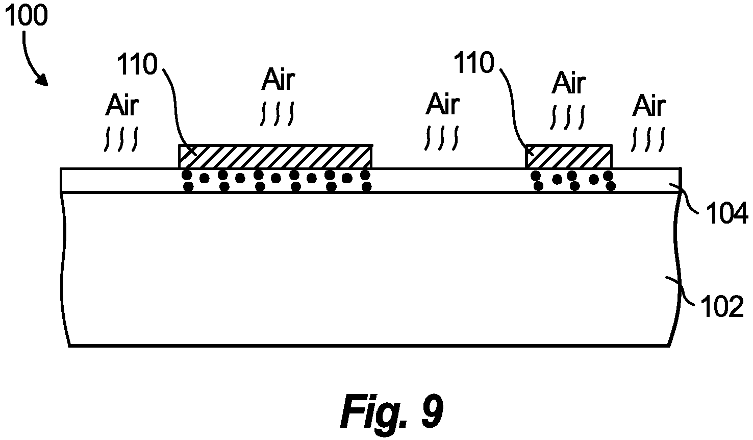
Fig. 9 is a schematic cross-sectional elevation view of the window or optic ofFig. 8 , showing an annealing process in air and the dopant atoms diffused through the semiconductor coating to the substrate; -
Fig. 10 is a schematic cross-sectional elevation view of the window or optic ofFig. 9 , showing the silicon oxynitride removed to leave the electrically conductive pattern in the semiconductor coating; -
Fig. 11 is a schematic cross-sectional elevation view of the window or optic ofFig. 1 , showing another embodiment of a method wherein the semiconductor coating is first coated with silicon oxynitride; -
Fig. 12 is a schematic cross-sectional elevation view of the window or optic ofFig. 11 , showing a layer of photoresist deposited on the silicon oxynitride; -
Fig. 13 is a schematic cross-sectional elevation view of the window or optic ofFig. 12 , showing a portion of the developed photoresist and the silicon oxynitride removed to allow doping of the semiconductor coating in a predetermined spatially varied pattern; -
Fig. 14 is a schematic cross-sectional elevation view of the window or optic ofFig. 13 , showing the photoresist removed and a doped pattern in the semiconductor coating; and -
Fig. 15 is a schematic cross-sectional elevation view of the window or optic ofFig. 14 , showing an annealing process in vacuum to form the electrically conductive pattern in the semiconductor coating, which after removal of the silicon oxynitride is as shown inFig. 10 . - Reference will now be made to the drawings wherein like reference numerals identify similar structural features or aspects of the subject disclosure. For purposes of explanation and illustration, and not limitation, a partial view of an exemplary embodiment of a window or optic in accordance with the disclosure is shown in
Fig. 1 and is designated generally byreference character 100. Other embodiments of windows or optics in accordance with the disclosure, or aspects thereof, are provided inFigs. 2-15 , as will be described. The systems and methods described herein can be used to provide spatially controlled or varied electrical conductivity in transparent oxide coatings for optics and windows. This can be used for electromagnetic interference (EMI) shielding, spatially varying sheet resistance for smart window applications, or any other suitable application. - Transparent, conductive oxides (TCO) such as indium tin oxide (ITO) and aluminum zinc oxide (AZO) are important coating materials for a wide variety of products that require optical transparency and electrical conductivity. The indium oxide (In2O3) and zinc oxide (ZnO) wide bandgap semiconductors have broadband optical transparency. The materials can be doped to provide electrical conductivity. However, as doping rises to increase electrical conductivity, optical transmittance decreases. This effect begins at longer wavelengths where both plasma reflectance and free-carrier absorption from electrons decrease transmittance. The common conductive oxide coatings are generally transparent only in the 0.4 to 2.0 micron wavelength range. This disclosure explains methods to spatially control the conductivity and transmittance of a transparent oxide thin film in different areas of a coating.
- A method of coating an
optical substrate 102 includes depositing asemiconductor coating 104 over a surface of anoptical substrate 102, e.g. over the entire surface of theoptical substrate 102. Depositing thesemiconductor coating 104 can include depositing thesemiconductor coating 104 with thesemiconductor coating 104 undoped, and in the presence of oxygen. Alternatively or in addition, oxide semiconductors can be annealed in air to provide excess oxygen in thesemiconductor coating 104. Thesemiconductor coating 104 has broadband optical transmittance as a transparent conducting oxide (TCO) material, and can include In2O3 , ZnO, or the like, e.g., wherein the electrical sheet resistance is greater than 2000 ohms/square. The semiconductor coating can therefore have broadband optical transmittance in at least visible and infrared spectra. - Portions of the
semiconductor coating 104 are doped to form a spatially varied pattern of doped semiconductor in the semiconductor coating as described further below. Doping portions of the semiconductor coating to form a spatially varied pattern can include applying dopant by ion implantation of donor atoms. Any other suitable technique can be used without departing from the scope of this disclosure, such as spin-on or spray-on dopant solutions. The doped semiconductor can include at least one of Sn, Mo, W, Ti, Al, or Ga. Hydrogen can serve as an electron donor and can passivate defects. - The method includes annealing the
semiconductor coating 104 to diffuse the dopant atoms through the semiconductor coating and to do at least one of: increase oxygen in undoped areas of the semiconductor coating; or reduce oxygen in doped areas of the semiconductor coating. Each of these is described below. - First, annealing the
semiconductor coating 104 can include thermal annealing and/or laser annealing in a predetermined pattern to improve crystal quality of the TCO materials of thesemiconductor coating 104 and increase electrical conductivity in doped areas of thesemiconductor coating 104. Annealing thesemiconductor coating 104 can include annealing in air to activate and diffuse dopant and increase oxygen in undoped areas of thesemiconductor coating 104. Doping portions of the semiconductor coating can include applying aphotoresist 106 over the semiconductor coating as shown inFig. 2 . The photoresist is selectively exposed and developed in the predetermined, spatially varied pattern, i.e., any pattern can be used, but inFig. 3 spatial variation in the pattern includes a wider opening inphotoresist 106 on the left than on the right opening in thephotoresist 106. The method includes doping thesemiconductor coating 104 through theopenings 105 in thephotoresist 106, as indicated by the downward arrows shown inFig. 3 . With reference toFig. 4 , thephotoresist 106 is removed, e.g., using a solvent, to leave the dopedsemiconductor 108 in the pattern in thesemiconductor coating 104. A coating ofsilicon oxynitride 110 is applied using plasma-enhanced chemical vapor deposition (PECVD) or the like over the entire surface of thesemiconductor coating 104, as shown inFig. 5 . Hydrogen in the PECVD process increases conductivity by adding electrons and passivating defects in oxide semiconductors. A hydrogen plasma can also be used. While silicon oxynitride is used as an example herein, those skilled in the art will readily appreciate that any other suitable protective film can be used without departing from the scope of this disclosure. Anotherphotoresist 112 is applied over thesilicon oxynitride 110, as shown inFig. 6 . Thisphotoresist 112 is exposed and developed in the inverse pattern of thefirst photoresist 106, and portions of the silicon oxynitride not covered by photoresist are removed as shown inFig. 7 , e.g., using diluted hydrofluoric acid (HF:H2O). The remainingphotoresist 112 is removed as shown in inFig. 8 , to prepare the substrate for annealing. The method includes annealing thesemiconductor coating 104, including annealing thesilicon oxynitride 110 andsemiconductor coating 104 in air, as indicated inFig. 9 , to activate and diffuse dopant and increase oxygen in undoped areas of thesemiconductor coating 104. The sheet resistance of undoped In2O3 can be increased from <100 ohms/square to >2000 ohms/square by increasing oxygen with air annealing. The remaining portions ofsilicon oxynitride 110 can then be removed from the substrate as shown inFig. 10 , where the activated, annealed dopant indoped areas 108 forms the predetermined, electrically conductive pattern insemiconductor coating 104. - Doping
portions 108 of thesemiconductor coating 104 and annealing thesemiconductor coating 104 can include diffusing the doped semiconductor through thesemiconductor coating 104 to theoptical substrate 102, i.e. the dopant diffuses all the way through the thickness of thesemiconductor coating 104, as shown inFig. 10 . The top surface of thesemiconductor coating 104 can be covered in its entirety with the pattern, which can be varied spatially to achieve any desired electrical conductivity as a function of two-dimensional location on the window oroptic 100. The optic orwindow 100 can thus be formed into a window having an electrically conductive coating, with broadband transparency, without etching and/or without polishing or post-process planarization. The activated dopedsemiconductor portions 108 and thesemiconductor coating 104 can have closely matched indices of refraction to mitigate light scattering from the pattern. If the ratio of the indices of refraction of the doped semiconductor and semiconductor coating is between 0.82 and 1.22, the interface reflection will be less than 1% at normal incidence. For example, the indices of refraction of doped and undoped In2O3 at 632.8 nm are about 2.00 and 1.77, respectively. The index ratio of 1.13 produces a reflection of only 0.37%. - The resulting window or optic 100 shown in
Fig. 10 includes a transparent substrate, i.e.optical substrate 102, with a coating over the transparent substrate, the coating being made of both a transparent semiconductor and an electrically conductive semiconductor, i.e., asemiconductor coating 104 with electricallyconductive portions 108. - With reference now to
Figs. 11-15 , another method is described, wherein after thesemiconductor coating 104 is deposited as shown inFig. 11 , a coating ofsilicon oxynitride 110 is applied over the entire surface of thesemiconductor coating 104 with the semiconductor undoped. Aphotoresist 106 is applied over thesilicon oxynitride 110, as shown inFig. 12 , and thephotoresist 106 is exposed and developed. The developedphotoresist 106 protects portions of thesilicon oxynitride 110, and the unprotected portions ofsilicon oxynitride 110 are removed to exposeportions 108 of thesemiconductor coating 104 as shown inFig. 13 . As indicated by the downward arrows inFig. 13 , thesemiconductor coating 104 is doped throughopenings 105 in thephotoresist 106. Optionally, thephotoresist 106 could be removed before doping, otherwise, thephotoresist 106 is removed after doping as shown inFig. 14 to leave the dopedsemiconductor portions 108 in the pattern in thesemiconductor coating 104. Annealing thesilicon oxynitride 110 andsemiconductor coating 104 under vacuum, as indicated inFig. 15 , activates and diffuses the dopant and reduces oxygen in doped areas, i.e.portions 108, of thesemiconductor coating 104. Oxygen vacancies contribute electrons and increase conductivity in oxide semiconductors. Without adding dopant atoms the sheet resistance of In2O3 can be reduced from >2000 ohms/square to <100 ohms/square by reducing oxygen with vacuum annealing. Thesilicon oxynitride 110 can then be removed to arrive at the structure shown inFig. 10 . - This disclosure relates to transparent conductive oxides (TCO) or oxide semiconductors where there is an increase or decrease of oxygen in selected areas during an annealing process. These oxygen changes decrease or increase the electron concentration and conductivity of the semiconductor, respectively. The sheet resistance of undoped In203 can be changed from >2000 ohms/square to <100 ohms/square and vice-versa by decreasing and increasing oxygen, respectively.
- The methods and systems of the present disclosure, as described above and shown in the drawings, provide for optical coatings with superior properties including spatially controlled electrical conductivity for broadband windows and optics. While the apparatus and methods of the subject disclosure have been shown and described with reference to preferred embodiments, those skilled in the art will readily appreciate that changes and/or modifications may be made thereto without departing from the scope of the subject disclosure.
- Preferred embodiments of the present disclosure are as follows:
- 1. A method of coating an optical substrate, comprising:
- depositing a semiconductor coating over a surface of an optical substrate, wherein the semiconductor coating has broadband optical transmittance;
- doping portions of the semiconductor coating to form a spatially varied pattern of doped semiconductor in the semiconductor coating; and
- annealing the semiconductor coating to do at least one of:
- increase oxygen in undoped areas of the semiconductor coating; or
- reduce oxygen in doped areas of the semiconductor coating.
- 2. The method as recited in embodiment 1, wherein annealing the semiconductor coating includes laser annealing in a predetermined pattern to improve crystal quality of transparent conducting oxide (TCO) materials of the semiconductor coating and increase electrical conductivity in doped areas of the semiconductor coating.
- 3. The method as recited in embodiment 1, wherein annealing the semiconductor coating includes annealing in air to activate and diffuse dopant and increase oxygen in undoped areas of the semiconductor coating.
- 4. The method as recited in embodiment 1, wherein doping portions of the semiconductor coating includes:
- applying a photoresist over the semiconductor coating;
- selectively exposing the photoresist;
- developing the photoresist in the pattern;
- doping the semiconductor coating through openings in the photoresist;
- removing the photoresist to leave the doped semiconductor in the pattern on the semiconductor coating;
- applying a coating of silicon oxynitride over the entire surface of the semiconductor coating;
- applying a photoresist over the silicon oxynitride, exposing the photoresist, and developing the photoresist;
- removing portions of the silicon oxynitride not covered by photoresist and then removing any remaining photoresist; and
- wherein annealing the semiconductor coating includes annealing the silicon oxynitride and semiconductor coating in air to activate and diffuse dopant and increase oxygen in undoped areas of the semiconductor coating.
- 5. The method as recited in embodiment 1, wherein annealing the semiconductor coating includes annealing under vacuum to activate and diffuse dopant and reduce oxygen in doped areas of the semiconductor coating.
- 6. The method as recited in embodiment 1, wherein doping portions of the semiconductor coating includes:
- applying a coating of silicon oxynitride over the entire surface of the semiconductor coating with the semiconductor undoped;
- applying a photoresist over the silicon oxynitride, exposing the photoresist, and developing the photoresist;
- removing portions of the silicon oxynitride not covered by photoresist;
- doping the semiconductor coating through openings in the photoresist;
- removing the photoresist to leave the doped semiconductor in the pattern on the semiconductor coating; and
- wherein annealing the semiconductor coating includes annealing the silicon oxynitride and semiconductor coating in vacuum to activate and diffuse dopant and reduce oxygen in doped areas of the semiconductor coating.
- 7. A method as recited in embodiment 1, wherein the semiconductor coating includes at least one of In2O3 or ZnO.
- 8. A method as recited in embodiment 1, wherein doping portions of the semiconductor coating to form a spatially varied pattern includes applying dopant by ion implantation.
- 9. A method as recited in embodiment 1, wherein the doped semiconductor includes at least one of Sn, Mo, W, Ti, Al, or Ga.
- 10. A method as recited in embodiment 1, wherein the semiconductor coating has broadband optical transmittance in at least visible and infrared spectra.
- 11. A method as recited in embodiment 1, wherein depositing the semiconductor coating includes depositing the semiconductor coating with the semiconductor coating undoped.
- 12. A method as recited in embodiment 1, wherein doping portions of the semiconductor coating and annealing the semiconductor coating include diffusing dopant atoms through the semiconductor coating to the optical substrate.
- 13. A method as recited in embodiment 1, wherein depositing a semiconductor coating includes depositing the semiconductor coating over a surface of the optical substrate in its entirety.
- 14. A method as recited in embodiment 1, wherein doping portions of the semiconductor coating to form a spatially varied pattern includes doping a surface of the semiconductor coating so a surface of the semiconductor coating is covered in its entirety with the pattern.
- 15. A method as recited in embodiment 1, wherein the semiconductor coating including annealed activated doped semiconductor in the semiconductor coating and the optical substrate are formed into a window without etching.
- 16. A method as recited in embodiment 1, wherein the semiconductor coating including annealed activated doped semiconductor in the semiconductor coating and the optical substrate are formed into a window without polishing or post-process planarization.
- 17. A method as recited in embodiment 1, wherein the activated doped semiconductor and semiconductor coating have closely matched indices of refraction to mitigate light scattering.
- 18. A method as recited in embodiment 1, further comprising making the doped semiconductor electrically conductive.
- 19. A method as recited in embodiment 1, further comprising adding hydrogen to the doped semiconductor by plasma-enhanced chemical vapor deposition (PECVD) silicon oxynitride process or by a hydrogen plasma.
- 20. A window comprising:
a transparent substrate with a coating over the transparent substrate, the coating being made of both a transparent semiconductor and an electrically conductive semiconductor with lower transparency than the transparent semiconductor, the electrically conductive semiconductor being annealed and distributed in a spatially varied pattern in the transparent semiconductor. - 21. The window as recited in embodiment 20, wherein the electrically conductive semiconductor is laser annealed.
- 22. The window as recited in embodiment 20, wherein the transparent semiconductor coating includes a transparent conducting oxide (TCO) material, and wherein the electrically conductive semiconductor includes a semiconductor material doped for electrical conductivity, wherein the doped semiconductor includes at least one of Sn, Mo, W, Ti, Al, or Ga.
- 23. A method of coating an optical substrate, comprising:
- depositing a semiconductor coating over a surface of an optical substrate, wherein the semiconductor coating has broadband optical transmittance;
- doping portions of the semiconductor coating to form a spatially varied pattern of doped semiconductor in the semiconductor coating; and
- annealing the semiconductor coating to do at least one of:
increase oxygen in undoped areas of the semiconductor coating; or reduce oxygen in doped areas of the semiconductor coating.
- 24. The method as recited in embodiment 23, wherein doping portions of the semiconductor coating includes:
- applying a photoresist over the semiconductor coating;
- selectively exposing the photoresist;
- developing the photoresist in the pattern;
- doping the semiconductor coating through openings in the photoresist;
- removing the photoresist to leave the doped semiconductor in the pattern on the semiconductor coating;
- applying a coating of silicon oxynitride over the entire surface of the semiconductor coating;
- applying a photoresist over the silicon oxynitride, exposing the photoresist, and developing the photoresist;
- removing portions of the silicon oxynitride not covered by photoresist and then removing any remaining photoresist; and
- 25. The method as recited in embodiment 23, wherein doping portions of the semiconductor coating includes:
- applying a coating of silicon oxynitride over the entire surface of the semiconductor coating with the semiconductor undoped;
- applying a photoresist over the silicon oxynitride, exposing the photoresist, and developing the photoresist;
- removing portions of the silicon oxynitride not covered by photoresist;
- doping the semiconductor coating through openings in the photoresist;
- removing the photoresist to leave the doped semiconductor in the pattern on the semiconductor coating; and
- wherein annealing the semiconductor coating includes annealing the silicon oxynitride and semiconductor coating in vacuum to activate and diffuse dopant and reduce oxygen in doped areas of the semiconductor coating.
- 26. The method as recited in any one of embodiments 23-25, wherein annealing the semiconductor coating includes laser annealing in a predetermined pattern to improve crystal quality of transparent conducting oxide (TCO) materials of the semiconductor coating and increase electrical conductivity in doped areas of the semiconductor coating.
- 27. The method as recited in any one of embodiments 23-26, wherein annealing the semiconductor coating includes annealing in air or under vacuum to activate and diffuse dopant and increase oxygen in undoped areas of the semiconductor coating.
- 28. A method as recited in any one of embodiments 23-27, wherein the semiconductor coating includes at least one of In2O3 or ZnO and/or the semiconductor coating has broadband optical transmittance in at least visible and infrared spectra.
- 29. A method as recited in any one of embodiments 23-28, wherein doping portions of the semiconductor coating to form a spatially varied pattern includes applying dopant by ion implantation and/or wherein the doped semiconductor includes at least one of Sn, Mo, W, Ti, Al, or Ga.
- 30. A method as recited in any one of embodiments 23-29, wherein depositing the semiconductor coating includes depositing the semiconductor coating with the semiconductor coating undoped.
- 31. A method as recited in any one of embodiments 23-30, wherein doping portions of the semiconductor coating and annealing the semiconductor coating include diffusing dopant atoms through the semiconductor coating to the optical substrate.
- 32. A method as recited in any one of embodiments 23-31, wherein depositing a semiconductor coating includes depositing the semiconductor coating over a surface of the optical substrate in its entirety.
- 33. A method as recited in any one of embodiments 23-32, wherein doping portions of the semiconductor coating to form a spatially varied pattern includes doping a surface of the semiconductor coating so a surface of the semiconductor coating is covered in its entirety with the pattern.
- 34. A method as recited in any one of embodiments 23-33, wherein the semiconductor coating including annealed activated doped semiconductor in the semiconductor coating and the optical substrate are formed into a window without etching and/or without polishing or post-process planarization.
- 35. A method as recited in any one of embodiments 23-34, wherein the activated doped semiconductor and semiconductor coating have closely matched indices of refraction to mitigate light scattering from the pattern.
- 36. A method as recited in any one of embodiments 23-35, further comprising making the doped semiconductor electrically conductive and/or further comprising adding hydrogen to the doped semiconductor by plasma-enhanced chemical vapor deposition (PECVD) silicon oxynitride process or by a hydrogen plasma.
- 37. A window comprising:
- a transparent substrate with a coating over the transparent substrate, the coating being made of both a transparent semiconductor and an electrically conductive semiconductor with lower transparency than the transparent semiconductor, the electrically conductive semiconductor being annealed and distributed in a spatially varied pattern in the transparent semiconductor,
- preferably wherein the electrically conductive semiconductor is laser annealed
- and/or wherein the transparent semiconductor coating includes a transparent conducting oxide (TCO) material, the electrically conductive semiconductor includes a semiconductor material doped for electrical conductivity, and the doped semiconductor includes at least one of Sn, Mo, W, Ti, Al, or Ga.
Claims (15)
- A method of coating an optical substrate, said method comprising:depositing a semiconductor coating over a surface of an optical substrate, wherein the semiconductor coating has broadband optical transmittance;doping portions of the semiconductor coating to form a spatially varied pattern of doped semiconductor in the semiconductor coating; andannealing the semiconductor coating.
- The method as recited in claim 1, wherein said annealing is to do at least one of:increase oxygen in undoped areas of the semiconductor coating; orreduce oxygen in doped areas of the semiconductor coating.
- The method as recited in claim 1 or claim 2, wherein annealing the semiconductor coating includes annealing in air to activate and diffuse dopant and increase oxygen in undoped areas of the semiconductor coating.
- The method as recited in claim 1 or claim 2, wherein annealing the semiconductor coating includes annealing under vacuum to activate and diffuse dopant and reduce oxygen in doped areas of the semiconductor coating.
- The method as recited in any one of the preceding claims, comprising applying a protective film over the entire surface of the semiconductor coating.
- The method as recited in claim 5, wherein said protective film is a coating of silicon oxynitride.
- The method as recited in claim 5 or claim 6, wherein the protective film is applied using plasma-enhanced chemical vapour deposition.
- The method as recited in any one of the preceding claims, wherein the semiconductor coating includes at least one of In2O3 or ZnO.
- The method as recited in any one of the preceding claims, wherein annealing the semiconductor coating includes laser annealing in a predetermined pattern to improve crystal quality of transparent conducting oxide (TCO) materials of the semiconductor coating and increase electrical conductivity in doped areas of the semiconductor coating.
- The method as recited in any one of the preceding claims, wherein doping portions of the semiconductor coating to form a spatially varied pattern includes applying dopant by ion implantation.
- The method as recited in any one of the preceding claims, wherein the doped semiconductor includes at least one of Sn, Mo, W, Ti, Al, or Ga.
- The method as recited in any one of the preceding claims, comprising adding hydrogen to the doped semiconductor by plasma-enhanced chemical vapor deposition (PECVD) silicon oxynitride process or by a hydrogen plasma.
- The method as recited in any one of the preceding claims, wherein doping portions of the semiconductor coating to form a spatially varied pattern includes doping a surface of the semiconductor coating so a surface of the semiconductor coating is covered in its entirety with the pattern.
- The method as recited in claim 1, wherein doping portions of the semiconductor coating includes:applying a photoresist over the semiconductor coating;selectively exposing the photoresist;developing the photoresist in the pattern;doping the semiconductor coating through openings in the photoresist;removing the photoresist to leave the doped semiconductor in the pattern on the semiconductor coating;applying a coating of silicon oxynitride over the entire surface of the semiconductor coating;applying a photoresist over the silicon oxynitride, exposing the photoresist, and developing the photoresist;removing portions of the silicon oxynitride not covered by photoresist and then removing any remaining photoresist; andwherein annealing the semiconductor coating includes annealing the silicon oxynitride and semiconductor coating in air to activate and diffuse dopant and increase oxygen in undoped areas of the semiconductor coating.
- The method as recited in claim 1, wherein doping portions of the semiconductor coating includes:applying a coating of silicon oxynitride over the entire surface of the semiconductor coating with the semiconductor undoped;applying a photoresist over the silicon oxynitride, exposing the photoresist, and developing the photoresist;removing portions of the silicon oxynitride not covered by photoresist;doping the semiconductor coating through openings in the photoresist;removing the photoresist to leave the doped semiconductor in the pattern on the semiconductor coating; andwherein annealing the semiconductor coating includes annealing the silicon oxynitride and semiconductor coating in vacuum to activate and diffuse dopant and reduce oxygen in doped areas of the semiconductor coating.
Applications Claiming Priority (2)
| Application Number | Priority Date | Filing Date | Title |
|---|---|---|---|
| US15/457,021 US9952355B1 (en) | 2017-03-13 | 2017-03-13 | Spatially controlled conductivity in transparent oxide coatings |
| EP18161230.0A EP3376840B1 (en) | 2017-03-13 | 2018-03-12 | Spatially controlled conductivity in transparent oxide coatings |
Related Parent Applications (1)
| Application Number | Title | Priority Date | Filing Date |
|---|---|---|---|
| EP18161230.0A Division EP3376840B1 (en) | 2017-03-13 | 2018-03-12 | Spatially controlled conductivity in transparent oxide coatings |
Publications (1)
| Publication Number | Publication Date |
|---|---|
| EP4152909A1 true EP4152909A1 (en) | 2023-03-22 |
Family
ID=61951835
Family Applications (2)
| Application Number | Title | Priority Date | Filing Date |
|---|---|---|---|
| EP18161230.0A Active EP3376840B1 (en) | 2017-03-13 | 2018-03-12 | Spatially controlled conductivity in transparent oxide coatings |
| EP22182912.0A Pending EP4152909A1 (en) | 2017-03-13 | 2018-03-12 | Spatially controlled conductivity in transparent oxide coatings |
Family Applications Before (1)
| Application Number | Title | Priority Date | Filing Date |
|---|---|---|---|
| EP18161230.0A Active EP3376840B1 (en) | 2017-03-13 | 2018-03-12 | Spatially controlled conductivity in transparent oxide coatings |
Country Status (3)
| Country | Link |
|---|---|
| US (1) | US9952355B1 (en) |
| EP (2) | EP3376840B1 (en) |
| JP (4) | JP7120776B2 (en) |
Families Citing this family (2)
| Publication number | Priority date | Publication date | Assignee | Title |
|---|---|---|---|---|
| US10126656B2 (en) * | 2016-09-08 | 2018-11-13 | Goodrich Corporation | Apparatus and methods of electrically conductive optical semiconductor coating |
| WO2021062162A1 (en) * | 2019-09-26 | 2021-04-01 | Raytheon Company | Method for protecting ir transmitting windows and domes from emi |
Citations (3)
| Publication number | Priority date | Publication date | Assignee | Title |
|---|---|---|---|---|
| JPS5125996A (en) * | 1974-08-28 | 1976-03-03 | Hitachi Ltd | |
| FR2967506A1 (en) * | 2010-11-16 | 2012-05-18 | Thales Sa | OPTRONIC TRANSPARENT IR TRANSPARENT AND RF REFLECTIVE |
| US9276034B2 (en) | 2014-04-07 | 2016-03-01 | Goodrich Corporation | Grid topography for patterned semiconductor coating that minimizes optical scatter and obscuration |
Family Cites Families (23)
| Publication number | Priority date | Publication date | Assignee | Title |
|---|---|---|---|---|
| US4093357A (en) | 1977-04-05 | 1978-06-06 | Hughes Aircraft Company | Cermet interface for electro-optical devices |
| JPS544395A (en) * | 1977-06-10 | 1979-01-13 | Matsushita Electric Ind Co Ltd | Eproduction method of transparent electrode |
| JPS5638084A (en) * | 1979-09-05 | 1981-04-13 | Sharp Kk | Patterning of transparent electroconductive film |
| JPS57174808A (en) * | 1981-04-17 | 1982-10-27 | Sharp Kk | Method of forming electrode pattern |
| US4395467A (en) * | 1981-12-30 | 1983-07-26 | Rca Corporation | Transparent conductive film having areas of high and low resistivity |
| JPS61190815A (en) * | 1985-02-18 | 1986-08-25 | 大阪特殊合金株式会社 | Formation of transparent conductive film pattern |
| JPS6374033A (en) * | 1986-09-18 | 1988-04-04 | Canon Inc | Formation of pattern |
| JP2522014B2 (en) * | 1988-05-26 | 1996-08-07 | カシオ計算機株式会社 | Method of forming transparent electrode |
| US5217539A (en) * | 1991-09-05 | 1993-06-08 | The Boeing Company | III-V solar cells and doping processes |
| FR2695117B1 (en) * | 1992-08-28 | 1994-12-02 | Saint Gobain Vitrage Int | Process for treating thin layers with electrical conduction and / or reflection properties in the infrared. |
| US7083880B2 (en) * | 2002-08-15 | 2006-08-01 | Freescale Semiconductor, Inc. | Lithographic template and method of formation and use |
| JP4425530B2 (en) * | 2002-08-20 | 2010-03-03 | 日揮触媒化成株式会社 | Method for producing indium oxide fine particles, coating liquid for forming transparent conductive film containing fine particles, substrate with transparent conductive film, and display device |
| CN1292448C (en) * | 2003-06-24 | 2006-12-27 | 精工爱普生株式会社 | Heating element, heating substrate, manufacturing method of heating substrate, micro switch, and fluid sensor |
| DE102005038441B4 (en) * | 2005-08-12 | 2010-08-05 | Infineon Technologies Ag | Field effect semiconductor device and method for producing the same |
| US8236680B2 (en) | 2008-06-20 | 2012-08-07 | Northwestern University | Nanoscale, spatially-controlled Ga doping of undoped transparent conducting oxide films |
| JP5455753B2 (en) * | 2009-04-06 | 2014-03-26 | 株式会社半導体エネルギー研究所 | IC card |
| CN102468166B (en) * | 2010-10-29 | 2015-01-28 | 中国科学院微电子研究所 | Transistor and its manufacturing method |
| EP2673674B1 (en) | 2011-02-09 | 2018-10-17 | Kinestral Technologies, Inc. | Electrochromic multi-layer devices with spatially coordinated switching |
| JP5887024B2 (en) | 2012-08-08 | 2016-03-16 | キネストラル・テクノロジーズ・インコーポレイテッドKinestral Technologies,Inc. | Electrochromic multilayer device with composite electrically conductive layer |
| WO2014025921A1 (en) | 2012-08-08 | 2014-02-13 | Kinestral Technologies, Inc. | Electrochromic multi-layer devices with current modulating structure |
| FR3002768B1 (en) * | 2013-03-01 | 2015-02-20 | Saint Gobain | PROCESS FOR THERMALLY TREATING A COATING |
| US9249504B2 (en) | 2013-09-26 | 2016-02-02 | Eastman Kodak Company | Method of passivating ultra-thin AZO with nano-layer alumina |
| US9842938B2 (en) * | 2015-03-24 | 2017-12-12 | Semiconductor Energy Laboratory Co., Ltd. | Semiconductor device and display device including semiconductor device |
-
2017
- 2017-03-13 US US15/457,021 patent/US9952355B1/en active Active
-
2018
- 2018-03-12 EP EP18161230.0A patent/EP3376840B1/en active Active
- 2018-03-12 EP EP22182912.0A patent/EP4152909A1/en active Pending
- 2018-03-13 JP JP2018044925A patent/JP7120776B2/en active Active
-
2022
- 2022-08-04 JP JP2022124541A patent/JP7458131B2/en active Active
-
2024
- 2024-03-14 JP JP2024039863A patent/JP2024061844A/en active Pending
-
2025
- 2025-11-17 JP JP2025196661A patent/JP2026012563A/en active Pending
Patent Citations (3)
| Publication number | Priority date | Publication date | Assignee | Title |
|---|---|---|---|---|
| JPS5125996A (en) * | 1974-08-28 | 1976-03-03 | Hitachi Ltd | |
| FR2967506A1 (en) * | 2010-11-16 | 2012-05-18 | Thales Sa | OPTRONIC TRANSPARENT IR TRANSPARENT AND RF REFLECTIVE |
| US9276034B2 (en) | 2014-04-07 | 2016-03-01 | Goodrich Corporation | Grid topography for patterned semiconductor coating that minimizes optical scatter and obscuration |
Also Published As
| Publication number | Publication date |
|---|---|
| JP2018163339A (en) | 2018-10-18 |
| JP2022183144A (en) | 2022-12-08 |
| JP2026012563A (en) | 2026-01-23 |
| JP7120776B2 (en) | 2022-08-17 |
| JP7458131B2 (en) | 2024-03-29 |
| JP2024061844A (en) | 2024-05-08 |
| EP3376840A1 (en) | 2018-09-19 |
| EP3376840B1 (en) | 2022-07-06 |
| US9952355B1 (en) | 2018-04-24 |
Similar Documents
| Publication | Publication Date | Title |
|---|---|---|
| US12399430B2 (en) | Apparatus and methods of electrically conductive optical semiconductor coating | |
| Treharne et al. | Optical design and fabrication of fully sputtered CdTe/CdS solar cells | |
| JP2026012563A (en) | Optical substrate coating method and window | |
| JP7593978B2 (en) | Apparatus and method for conductive photo-semiconductor coatings | |
| JP7226939B2 (en) | MWIR/LWIR transparent conductive coatings | |
| WO2015199624A1 (en) | A graphene based emi shielding optical coating | |
| CN107667077B (en) | Substrate provided with a stack of metal-containing terminal layers and oxide pre-terminal layers having thermal properties | |
| CN103570254B (en) | Conductive glass, its preparation method and application | |
| KR102477458B1 (en) | Substrate provided with a stack having thermal properties and having a metal terminal layer | |
| Buckley et al. | Optical reflectance of solution processed quasi-superlattice ZnO and Al-doped ZnO (AZO) channel materials | |
| JPH08227063A (en) | Conductive window that transmits long-wave infrared |
Legal Events
| Date | Code | Title | Description |
|---|---|---|---|
| PUAI | Public reference made under article 153(3) epc to a published international application that has entered the european phase |
Free format text: ORIGINAL CODE: 0009012 |
|
| STAA | Information on the status of an ep patent application or granted ep patent |
Free format text: STATUS: THE APPLICATION HAS BEEN PUBLISHED |
|
| AC | Divisional application: reference to earlier application |
Ref document number: 3376840 Country of ref document: EP Kind code of ref document: P |
|
| AK | Designated contracting states |
Kind code of ref document: A1 Designated state(s): AL AT BE BG CH CY CZ DE DK EE ES FI FR GB GR HR HU IE IS IT LI LT LU LV MC MK MT NL NO PL PT RO RS SE SI SK SM TR |
|
| STAA | Information on the status of an ep patent application or granted ep patent |
Free format text: STATUS: REQUEST FOR EXAMINATION WAS MADE |
|
| 17P | Request for examination filed |
Effective date: 20230921 |
|
| RBV | Designated contracting states (corrected) |
Designated state(s): AL AT BE BG CH CY CZ DE DK EE ES FI FR GB GR HR HU IE IS IT LI LT LU LV MC MK MT NL NO PL PT RO RS SE SI SK SM TR |
|
| STAA | Information on the status of an ep patent application or granted ep patent |
Free format text: STATUS: EXAMINATION IS IN PROGRESS |
|
| 17Q | First examination report despatched |
Effective date: 20260226 |