EP4152601A1 - Mehrkernoszillator mit transienter versorgungsspannungsunterstützter modusumschaltung - Google Patents
Mehrkernoszillator mit transienter versorgungsspannungsunterstützter modusumschaltung Download PDFInfo
- Publication number
- EP4152601A1 EP4152601A1 EP22190063.2A EP22190063A EP4152601A1 EP 4152601 A1 EP4152601 A1 EP 4152601A1 EP 22190063 A EP22190063 A EP 22190063A EP 4152601 A1 EP4152601 A1 EP 4152601A1
- Authority
- EP
- European Patent Office
- Prior art keywords
- circuitry
- voltage
- mode
- controlled oscillator
- switching
- Prior art date
- Legal status (The legal status is an assumption and is not a legal conclusion. Google has not performed a legal analysis and makes no representation as to the accuracy of the status listed.)
- Pending
Links
Images






Classifications
-
- H—ELECTRICITY
- H03—ELECTRONIC CIRCUITRY
- H03B—GENERATION OF OSCILLATIONS, DIRECTLY OR BY FREQUENCY-CHANGING, BY CIRCUITS EMPLOYING ACTIVE ELEMENTS WHICH OPERATE IN A NON-SWITCHING MANNER; GENERATION OF NOISE BY SUCH CIRCUITS
- H03B5/00—Generation of oscillations using amplifier with regenerative feedback from output to input
- H03B5/02—Details
- H03B5/06—Modifications of generator to ensure starting of oscillations
-
- H—ELECTRICITY
- H03—ELECTRONIC CIRCUITRY
- H03B—GENERATION OF OSCILLATIONS, DIRECTLY OR BY FREQUENCY-CHANGING, BY CIRCUITS EMPLOYING ACTIVE ELEMENTS WHICH OPERATE IN A NON-SWITCHING MANNER; GENERATION OF NOISE BY SUCH CIRCUITS
- H03B5/00—Generation of oscillations using amplifier with regenerative feedback from output to input
- H03B5/08—Generation of oscillations using amplifier with regenerative feedback from output to input with frequency-determining element comprising lumped inductance and capacitance
- H03B5/12—Generation of oscillations using amplifier with regenerative feedback from output to input with frequency-determining element comprising lumped inductance and capacitance active element in amplifier being semiconductor device
-
- H—ELECTRICITY
- H03—ELECTRONIC CIRCUITRY
- H03L—AUTOMATIC CONTROL, STARTING, SYNCHRONISATION OR STABILISATION OF GENERATORS OF ELECTRONIC OSCILLATIONS OR PULSES
- H03L1/00—Stabilisation of generator output against variations of physical values, e.g. power supply
-
- H—ELECTRICITY
- H04—ELECTRIC COMMUNICATION TECHNIQUE
- H04B—TRANSMISSION
- H04B1/00—Details of transmission systems, not covered by a single one of groups H04B3/00 - H04B13/00; Details of transmission systems not characterised by the medium used for transmission
- H04B1/38—Transceivers, i.e. devices in which transmitter and receiver form a structural unit and in which at least one part is used for functions of transmitting and receiving
- H04B1/40—Circuits
-
- H—ELECTRICITY
- H04—ELECTRIC COMMUNICATION TECHNIQUE
- H04B—TRANSMISSION
- H04B1/00—Details of transmission systems, not covered by a single one of groups H04B3/00 - H04B13/00; Details of transmission systems not characterised by the medium used for transmission
- H04B1/38—Transceivers, i.e. devices in which transmitter and receiver form a structural unit and in which at least one part is used for functions of transmitting and receiving
- H04B1/40—Circuits
- H04B1/401—Circuits for selecting or indicating operating mode
-
- H—ELECTRICITY
- H03—ELECTRONIC CIRCUITRY
- H03B—GENERATION OF OSCILLATIONS, DIRECTLY OR BY FREQUENCY-CHANGING, BY CIRCUITS EMPLOYING ACTIVE ELEMENTS WHICH OPERATE IN A NON-SWITCHING MANNER; GENERATION OF NOISE BY SUCH CIRCUITS
- H03B2200/00—Indexing scheme relating to details of oscillators covered by H03B
- H03B2200/006—Functional aspects of oscillators
- H03B2200/0082—Lowering the supply voltage and saving power
-
- H—ELECTRICITY
- H03—ELECTRONIC CIRCUITRY
- H03B—GENERATION OF OSCILLATIONS, DIRECTLY OR BY FREQUENCY-CHANGING, BY CIRCUITS EMPLOYING ACTIVE ELEMENTS WHICH OPERATE IN A NON-SWITCHING MANNER; GENERATION OF NOISE BY SUCH CIRCUITS
- H03B2200/00—Indexing scheme relating to details of oscillators covered by H03B
- H03B2200/006—Functional aspects of oscillators
- H03B2200/0088—Reduction of noise
- H03B2200/009—Reduction of phase noise
-
- H—ELECTRICITY
- H03—ELECTRONIC CIRCUITRY
- H03B—GENERATION OF OSCILLATIONS, DIRECTLY OR BY FREQUENCY-CHANGING, BY CIRCUITS EMPLOYING ACTIVE ELEMENTS WHICH OPERATE IN A NON-SWITCHING MANNER; GENERATION OF NOISE BY SUCH CIRCUITS
- H03B2200/00—Indexing scheme relating to details of oscillators covered by H03B
- H03B2200/006—Functional aspects of oscillators
- H03B2200/0092—Measures to linearise or reduce distortion of oscillator characteristics
-
- H—ELECTRICITY
- H03—ELECTRONIC CIRCUITRY
- H03B—GENERATION OF OSCILLATIONS, DIRECTLY OR BY FREQUENCY-CHANGING, BY CIRCUITS EMPLOYING ACTIVE ELEMENTS WHICH OPERATE IN A NON-SWITCHING MANNER; GENERATION OF NOISE BY SUCH CIRCUITS
- H03B2201/00—Aspects of oscillators relating to varying the frequency of the oscillations
- H03B2201/03—Varying beside the frequency also another parameter of the oscillator in dependence on the frequency
- H03B2201/038—Varying beside the frequency also another parameter of the oscillator in dependence on the frequency the parameter being a bias voltage or a power supply
Definitions
- a local oscillator may include a voltage-controlled oscillation circuitry that generates a local oscillation signal.
- the local oscillator may be used in any suitable part of the electronic device to support a frequency range (e.g., a wide frequency range) and utilize switches to reconfigure operation of the local oscillator in different modes and/or frequencies, such as in a transceiver coupled to one or more antennas that enables the electronic device to both transmit and receive wireless signals, a high speed serialize/deserializer with wideband phase locked loop circuitry, and so on.
- the local oscillation signal may be mixed with a data signal to upconvert the data signal (e.g., to a higher or radio frequency) to generate a transmission signal to be transmitted via the one or more antennas, or downconvert a received signal (e.g., to a lower or baseband frequency) received via the one or more antennas to generate a data signal.
- a data signal e.g., to a higher or radio frequency
- a received signal e.g., to a lower or baseband frequency
- any exact values, numbers, measurements, and so on, provided herein, are contemplated to include approximations (e.g., within a margin of suitable or contemplatable error) of the exact values, numbers, measurements, and so on.
- This disclosure is directed to a local oscillator having voltage-controlled oscillation circuitry that generates a local oscillation signal.
- the local oscillator may be used in any suitable part of the electronic device to support a frequency range (e.g., a wide frequency range) and utilizes switches to reconfigure operation of the local oscillator in different modes and/or frequencies, such as in a transceiver coupled to one or more antennas that enables the electronic device to both transmit and receive wireless signals, a high speed serialize/deserializer with wideband phase locked loop circuitry, and so on.
- the present disclosure describes the local oscillator as part of a transceiver for exemplary purposes, but it should be understood that the local oscillator may be part of any suitable part of the electronic device, such as processing circuitry, memory, display circuitry, and so on of the electronic device.
- the electronic device may include a transceiver that may be coupled to one or more antennas to enable the device to both transmit and receive wireless signals.
- the transceiver may include a local oscillator having voltage-controlled oscillation circuitry that generates a local oscillation signal.
- the local oscillation signal may be mixed with a data signal to upconvert the data signal (e.g., to a higher or radio frequency) to generate a transmission signal to be transmitted via the one or more antennas, or downconvert a received signal (e.g., to a lower or baseband frequency) received via the one or more antennas to generate a data signal.
- a data signal e.g., to a higher or radio frequency
- a received signal e.g., to a lower or baseband frequency
- phase noise in wireless signals transmitted or received by a wireless communication device may result in lower data error vector magnitude, improved spectral purity, and, ultimately, superior performance.
- multi-core architecture becomes a promising approach, particularly for 5 th generation (5G) millimeter wave (mmWave) applications.
- phase noise may be reduced by a factor of 10 ⁇ log 10 (N) with N coupled oscillators.
- the wireless communication device may include a transceiver coupled to one or more antennas that enables the device to transmit and receive the wireless signals.
- the transceiver may include a local oscillator having voltage-controlled oscillation circuitry that generates a local oscillation signal.
- the local oscillation signal may be mixed with a data signal to upconvert the data signal (e.g., to a higher or radio frequency) to generate a transmission signal to be transmitted via the one or more antennas, or downconvert a received signal (e.g., to a lower or baseband frequency) received via the one or more antennas to generate a data signal.
- the voltage-controlled oscillation circuitry may include multiple cores (e.g., each core having its own LC tank circuit), and operate in multiple modes to generate signals having different frequencies, thus enlarging tuning range. For different operation modes, an oscillator is coupled to different load capacitances so the oscillation frequency may be varied over the modes. However, when the voltage-controlled oscillation circuitry is operating in a desired mode, another undesired mode may surpass and even dominate the desired mode. This may be because the undesired mode has greater gain (e.g., a larger loop gain) than that of the desired mode, which causes the undesired mode to increase more rapidly than the desired mode.
- gain e.g., a larger loop gain
- Loop gain may refer to a total gain of or around a feedback loop, which may feed an output back into an input, be measured in decibels, and indicate startup strength in a positive feedback-based oscillator. Indeed, this may be dependent upon an initial condition of system dynamics and/or external disturbances to the voltage-controlled oscillation circuitry. As a result of this dominant undesired mode of operation, the voltage-controlled oscillation circuitry may output a signal with an undesired frequency and/or undesired phase noise.
- FIG. 1 is a block diagram of an electronic device 10, according to embodiments of the present disclosure.
- the electronic device 10 may include, among other things, one or more processors 12 (collectively referred to herein as a single processor for convenience, which may be implemented in any suitable form of processing circuitry), memory 14, nonvolatile storage 16, a display 18, input structures 22, an input/output (I/O) interface 24, a network interface 26, and a power source 29.
- the various functional blocks shown in FIG. 1 may include hardware elements (including circuitry), software elements (including machine-executable instructions) or a combination of both hardware and software elements (which may be referred to as logic).
- the processor 12, memory 14, the nonvolatile storage 16, the display 18, the input structures 22, the input/output (I/O) interface 24, the network interface 26, and/or the power source 29 may each be communicatively coupled directly or indirectly (e.g., through or via another component, a communication bus, a network) to one another to transmit and/or receive data between one another.
- FIG. 1 is merely one example of a particular implementation and is intended to illustrate the types of components that may be present in electronic device 10.
- the electronic device 10 may include any suitable computing device, including a desktop or notebook computer (e.g., in the form of a MacBook ® , MacBook ® Pro, MacBook Air ® , iMac ® , Mac ® mini, or Mac Pro ® available from Apple Inc. of Cupertino, California), a portable electronic or handheld electronic device such as a wireless electronic device or smartphone (e.g., in the form of a model of an iPhone ® available from Apple Inc. of Cupertino, California), a tablet (e.g., in the form of a model of an iPad ® available from Apple Inc. of Cupertino, California), a wearable electronic device (e.g., in the form of an Apple Watch ® by Apple Inc.
- a desktop or notebook computer e.g., in the form of a MacBook ® , MacBook ® Pro, MacBook Air ® , iMac ® , Mac ® mini, or Mac Pro ® available from Apple Inc. of Cupertino, California
- the processor 12 may be implemented with any combination of general-purpose microprocessors, microcontrollers, digital signal processors (DSPs), field programmable gate array (FPGAs), programmable logic devices (PLDs), controllers, state machines, gated logic, discrete hardware components, dedicated hardware finite state machines, or any other suitable entities that may perform calculations or other manipulations of information.
- the processors 12 may include one or more application processors, one or more baseband processors, or both, and perform the various functions described herein.
- the processor 12 may be operably coupled with a memory 14 and a nonvolatile storage 16 to perform various algorithms.
- Such programs or instructions executed by the processor 12 may be stored in any suitable article of manufacture that includes one or more tangible, computer-readable media.
- the tangible, computer-readable media may include the memory 14 and/or the nonvolatile storage 16, individually or collectively, to store the instructions or routines.
- the memory 14 and the nonvolatile storage 16 may include any suitable articles of manufacture for storing data and executable instructions, such as random-access memory, read-only memory, rewritable flash memory, hard drives, and optical discs.
- programs e.g., an operating system
- encoded on such a computer program product may also include instructions that may be executed by the processor 12 to enable the electronic device 10 to provide various functionalities.
- the input structures 22 of the electronic device 10 may enable a user to interact with the electronic device 10 (e.g., pressing a button to increase or decrease a volume level).
- the I/O interface 24 may enable electronic device 10 to interface with various other electronic devices, as may the network interface 26.
- the I/O interface 24 may include an I/O port for a hardwired connection for charging and/or content manipulation using a standard connector and protocol, such as the Lightning connector provided by Apple Inc. of Cupertino, California, a universal serial bus (USB), or other similar connector and protocol.
- the network interface 26 may include, for example, one or more interfaces for a personal area network (PAN), such as an ultra-wideband (UWB) or a BLUETOOTH ® network, for a local area network (LAN) or wireless local area network (WLAN), such as a network employing one of the IEEE 802.11x family of protocols (e.g., WI-FI ® ), and/or for a wide area network (WAN), such as any standards related to the Third Generation Partnership Project (3GPP), including, for example, a 3 rd generation (3G) cellular network, universal mobile telecommunication system (UMTS), 4 th generation (4G) cellular network, long term evolution (LTE ® ) cellular network, long term evolution license assisted access (LTE-LAA) cellular network, 5 th generation (5G) cellular network, and/or New Radio (NR) cellular network, a satellite network, and so on.
- PAN personal area network
- UWB ultra-wideband
- WLAN wireless local area network
- the network interface 26 may include, for example, one or more interfaces for using a Release-15 cellular communication standard of the 5G specifications that include the millimeter wave (mmWave) frequency range (e.g., 24.25-300 gigahertz (GHz)) and/or any other cellular communication standard release (e.g., Release-16, Release-17, any future releases) that define and/or enable frequency ranges used for wireless communication.
- the network interface 26 of the electronic device 10 may allow communication over the aforementioned networks (e.g., 5G, Wi-Fi, LTE-LAA, and so forth).
- the network interface 26 may also include one or more interfaces for, for example, broadband fixed wireless access networks (e.g., WIMAX ® ), mobile broadband Wireless networks (mobile WIMAX ® ), asynchronous digital subscriber lines (e.g., ADSL, VDSL), digital video broadcasting-terrestrial (DVB-T ® ) network and its extension DVB Handheld (DVB-H ® ) network, ultra-wideband (UWB) network, alternating current (AC) power lines, and so forth.
- broadband fixed wireless access networks e.g., WIMAX ®
- mobile broadband Wireless networks e.g., mobile broadband Wireless networks (mobile WIMAX ® )
- asynchronous digital subscriber lines e.g., ADSL, VDSL
- DVD-T ® digital video broadcasting-terrestrial
- DVD-H ® extension DVB Handheld
- UWB ultra-wideband
- AC alternating current
- the network interface 26 may include a transceiver 30.
- the transceiver 30 may support transmission and receipt of various wireless signals via one or more antennas, and thus may include a transmitter and a receiver.
- the power source 29 of the electronic device 10 may include any suitable source of power, such as a rechargeable lithium polymer (Lipoly) battery and/or an alternating current (AC) power converter.
- FIG. 2 is a functional diagram of the electronic device 10 of FIG. 1 , according to embodiments of the present disclosure.
- the processor 12, the memory 14, the transceiver 30, a transmitter 52, a receiver 54, and/or antennas 55 may be communicatively coupled directly or indirectly (e.g., through or via another component, a communication bus, a network) to one another to transmit and/or receive data between one another.
- the electronic device 10 may include the transmitter 52 and/or the receiver 54 that respectively enable transmission and reception of data between the electronic device 10 and an external device via, for example, a network (e.g., including base stations) or a direct connection. As illustrated, the transmitter 52 and the receiver 54 may be combined into the transceiver 30.
- the electronic device 10 may also have one or more antennas 55A-55N electrically coupled to the transceiver 30.
- the antennas 55A-55N may be configured in an omnidirectional or directional configuration, in a single-beam, dual-beam, or multi-beam arrangement, and so on. Each antenna 55 may be associated with a one or more beams and various configurations.
- multiple antennas of the antennas 55A-55N of an antenna group or module may be communicatively coupled a respective transceiver 30 and each emit radio frequency signals that may constructively and/or destructively combine to form a beam.
- the electronic device 10 may include multiple transmitters, multiple receivers, multiple transceivers, and/or multiple antennas as suitable for various communication standards.
- the transmitter 52 and the receiver 54 may transmit and receive information via other wired or wireline systems or means.
- the various components of the electronic device 10 may be coupled together by a bus system 56.
- the bus system 56 may include a data bus, for example, as well as a power bus, a control signal bus, and a status signal bus, in addition to the data bus.
- the components of the electronic device 10 may be coupled together or accept or provide inputs to each other using some other mechanism.
- FIG. 3 is a block diagram of a transmitter 52 (e.g., transmit circuitry) that may be part of the transceiver 30, according to embodiments of the present disclosure.
- the transmitter 52 may receive outgoing data 60 in the form of a digital signal to be transmitted via the one or more antennas 55.
- a digital-to-analog converter (DAC) 62 of the transmitter 52 may convert the digital signal to an analog signal, and a modulator 63 may combine the converted analog signal with a carrier signal.
- a mixer 64 may combine the carrier signal with a local oscillator signal 65 from a local oscillator 66 to generate a radio frequency signal.
- the local oscillation 66 may include voltage-controlled oscillation (VCO) circuitry 67 that generates or facilitates generating the local oscillation signal 65.
- VCO voltage-controlled oscillation
- a power amplifier (PA) 68 receives the radio frequency signal from the mixer 64, and may amplify the modulated signal to a suitable level to drive transmission of the signal via the one or more antennas 55.
- a filter 69 e.g., filter circuitry and/or software
- the filter 69 may include any suitable filter or filters to remove the undesirable noise from the amplified signal, such as a bandpass filter, a bandstop filter, a low pass filter, a high pass filter, and/or a decimation filter.
- the transmitter 52 may include any suitable additional components not shown, or may not include certain of the illustrated components, such that the transmitter 52 may transmit the outgoing data 60 via the one or more antennas 55.
- the transmitter 52 may include an additional mixer and/or a digital up converter (e.g., for converting an input signal from a baseband frequency to an intermediate frequency).
- the transmitter 52 may not include the filter 69 if the power amplifier 68 outputs the amplified signal in or approximately in a desired frequency range (such that filtering of the amplified signal may be unnecessary).
- FIG. 4 is a schematic diagram of a receiver 54 (e.g., receive circuitry) that may be part of the transceiver 30, according to embodiments of the present disclosure.
- the receiver 54 may receive received data 80 from the one or more antennas 55 in the form of an analog signal.
- a low noise amplifier (LNA) 81 may amplify the received analog signal to a suitable level for the receiver 54 to process.
- a mixer 82 may combine the amplified signal with a local oscillation signal 83 from a local oscillator 84 to generate an intermediate or baseband frequency signal.
- the local oscillator 84 of the receiver 54 may include VCO circuitry 85 that generates or facilitates generating the local oscillation signal 83.
- a filter 86 may remove undesired noise from the signal, such as cross-channel interference.
- the filter 86 may also remove additional signals received by the one or more antennas 55 that are at frequencies other than the desired signal.
- the filter 86 may include any suitable filter or filters to remove the undesired noise or signals from the received signal, such as a bandpass filter, a bandstop filter, a low pass filter, a high pass filter, and/or a decimation filter.
- a demodulator 87 may remove a radio frequency envelope and/or extract a demodulated signal from the filtered signal for processing.
- An analog-to-digital converter (ADC) 88 may receive the demodulated analog signal and convert the signal to a digital signal of incoming data 90 to be further processed by the electronic device 10.
- the receiver 54 may include any suitable additional components not shown, or may not include certain of the illustrated components, such that the receiver 54 may receive the received data 80 via the one or more antennas 55.
- the receiver 54 may include an additional mixer and/or a digital down converter (e.g., for converting an input signal from an intermediate frequency to a baseband frequency).
- FIGS. 2-4 describe a transceiver 30 having a local oscillator 66, 84 that includes respective VCO circuitry 67, 85, it should be understood that the local oscillator 66, 84 may be part of any suitable part of the electronic device 10, such as the processor 12, the memory 14, the storage 16, the display 18, the input structures 22, the I/O interface 24, the power source 29, and so on of the electronic device 10.
- the local oscillator 66, 84 may be used in any suitable part of the electronic device 10 to support a frequency range (e.g., a wide frequency range) and utilizes switches to reconfigure operation of the local oscillator 66, 84 in different modes and/or frequencies, such as in a high speed serialize/deserializer with wideband phase locked loop circuitry.
- a frequency range e.g., a wide frequency range
- switches to reconfigure operation of the local oscillator 66, 84 in different modes and/or frequencies, such as in a high speed serialize/deserializer with wideband phase locked loop circuitry.
- Each core 102A, 102B may include a first terminal 104A, 104B and a second terminal 106A, 106B that may provide tap points for outputting signals from the core 102A, 102B.
- the first terminals 104A, 104B (collectively 104) and the second terminals 106A, 106B (collectively 106) may enable outputting a differential signal pair.
- each core 102A, 102B is also coupled to a respective inductor 108A, 108B (collectively 108).
- the two cores 102 may be coupled via one or more capacitances 110A, 110B (collectively 110), illustrated in FIG. 5 as a capacitor pair. It should be understood that the capacitances 110 may be provided by any suitable device or component, such as one or more capacitors.
- tank impedances e.g., impedances at the cores 102A, 102B
- This mode of operation may be referred to herein as a first mode or "Mode 0."
- the capacitances 110 may provide a greater capacitance between the cores 102A, 102B.
- the more out of phase the adjacent cores 102A, 102B are e.g., the greater the phase difference between the cores 102A, 102B
- the greater capacitance may be provided by the capacitances 110.
- the capacitances 110 may have an increased or maximum capacitance when the adjacent cores 102A, 102B are out of phase by 180°.
- FIG. 6 is a schematic diagram of the portion 100 of the VCO circuitry 67, 85 with the two cores 102 operating out of phase, according to embodiments of the current disclosure.
- the currents 112 in the inductors 108 of the cores 102 have the same (e.g., clockwise) direction.
- the first terminal 104A of the inductor 108A is negative and the second terminal 104A of the inductor 108A is positive.
- the first terminal 104B of the inductor 108B is negative, and the second terminal 106B of the inductor 108B is positive.
- the tank voltages are out of phase, and the capacitances 110 provide a larger (e.g., maximum) capacitance between the cores 102 and appear "visible.”
- the capacitances 110 are drawn in solidly.
- the tank impedances may have lower impedances (e.g., than when the adjacent cores 102A, 102B are in phase), such as decreased or minimum (e.g., zero or near zero) impedances.
- Mode 1 This operation may be referred to herein as a second mode or "Mode 1."
- Mode 1 has a large capacitance and smaller tank impedance, and hence a smaller loop gain, it may be overwhelmed by Mode 0 (which has a smaller capacitance and larger tank impedance, and hence a larger loop gain).
- the disclosed embodiments facilitate providing that a desired mode loop gain is larger than a threshold loop gain (e.g., 0 decibels (dB), 1 dB, and so on) while any other undesired mode startup loop gain is less than the threshold loop gain for a certain time window duration when oscillation starts up or mode is switched. This may provide sufficient gain within a time duration for the desired mode to develop into the dominant oscillation mode.
- a threshold loop gain e.g., 0 decibels (dB), 1 dB, and so on
- the processor 12 may provide a supply reset and ramp pulse when switching the VCO circuitry 67, 85 to a new mode, such that supply voltage to the VCO circuitry 67, 85 is reset (e.g., set to 0 V or another reference voltage), and gradually increased or ramped up back to a steady-state voltage (e.g., used to maintain a mode) within a time duration.
- the processor 12 may provide a switch control bootstrap pulse that is bootstrapped to (e.g., applied instantaneously or at the same time) switching the VCO circuitry 67, 85 to a new mode. After a time duration, the VCO circuitry 67, 85 may switch back to a steady-state voltage (e.g., used to maintain the new mode).
- FIG. 7 is a schematic diagram of a portion 120 of the VCO circuitry 67, 85 with switching circuitry 122, according to an embodiment of the present disclosure.
- the switching circuitry 122 may couple a first core (e.g., 102a) of the VCO circuitry 67, 85 to a second core (e.g., 102b), and couple or uncouple variable supply voltage to the VCO circuitry 67, 85.
- a first core e.g., 102a
- a second core e.g., 102b
- FIG. 8 is a block diagram of the switching circuitry 122, according to an embodiment of the present disclosure.
- the switching circuitry 122 may include terminal switching circuitry 130, which may couple each terminal (e.g., 104A, 106A) of a first core (e.g., 102A) to couple with another terminal (e.g., 104B, 106B) of a second core (e.g., 102B).
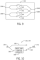
- FIG. 9 is circuit diagram of the terminal switching circuitry 130, according to an embodiment of the present disclosure.
- the terminal switching circuitry 130 includes a first switch 140 that may couple or uncouple a positive terminal (e.g., 104A) of the first core 102A to a positive terminal (e.g., 104B) of the second core 102B, a second switch 142 that may couple the positive terminal 104A of the first core 102A to a negative terminal (e.g., 106B) of the second core 102B, a third switch 144 that may couple a negative terminal (e.g., 106A) of the first core 102A to the positive terminal 104B of the second core 102B, and a fourth switch 146 that may couple the negative terminal 106A of the first core 102A to the negative terminal 106B of the second core 102B.
- the terminal switching circuitry 130 may be implemented as a phase swapper that includes a butterfly switch matrix and controls a phase relationship between adjacent oscillator
- the switching circuitry 122 may also include supply voltage switching circuitry 132.
- the supply voltage switching circuitry 132 may supply reset and ramp pulse when switching the VCO circuitry 67, 85 to a new mode.
- FIG. 10 is a schematic diagram of the supply voltage switching circuitry 132 (e.g., in the form of switch control reset and ramping circuitry 134) that may provide a reset and ramp pulse, according to embodiments of the present disclosure.
- a switch 162 may provide a steady-state supply voltage V in 164 (e.g., as provided by a power supply) to the VCO circuitry 67, 85 (e.g., to the cores 102 of the VCO circuitry 67, 85).
- the switch 162 may reset (e.g., using a reset pulse) the voltage supplied to the VCO circuitry 67, 85 (e.g., to 0 Volts or any other suitable reference voltage less than the steady-state supply voltage of V in 164), and gradually ramp up (e.g., increase in a linear fashion, using a ramp pulse) the supply voltage from 0 Volts to V in 164 over a certain time window, using reset and ramping circuitry 168.
- an output voltage V out 170 of the switch control reset and ramping circuitry 134 may be supplied to a switching core 102 (e.g., a core 102 that is switching operating modes). That is, the reset and ramping circuitry 168 may supply a ramp pulse to the switching core 102 via the output voltage V out 170.
- FIG. 11 is a combination timing diagram illustrating operation of the switch control reset and ramping circuitry 134 of FIG. 10 providing a reset and ramp pulse, according to embodiments of the present disclosure.
- the combination timing diagram of FIG. 11 illustrates mode control 180, oscillation supply 182, oscillation frequency 184, voltage waveform 186, and mode loop gain 188 over time 190.
- the processor 12 may cause the VCO circuitry 67, 85 to operate in a first mode 194 (e.g., Mode 0) as shown in the mode control 180 timing diagram.
- a first mode 194 e.g., Mode 0
- the processor 12 may supply the VCO circuitry 67, 85 with a steady-state supply voltage V in 196 (e.g., as provided by a power supply) as shown in the oscillation supply 182 diagram.
- V in 196 e.g., as provided by a power supply
- the VCO circuitry 67, 85 may oscillate at a frequency f0 198 corresponding to Mode 0 194 as shown in the oscillation frequency 184 diagram, and a voltage waveform 200 of the VCO circuitry 67, 85 is at a steady state (e.g., corresponding to Mode 0 194) as shown in the voltage waveform 186 diagram.
- a loop gain 204 corresponding to Mode 0 194 is greater than a loop gain 206 corresponding to over a second mode (e.g., Mode 1) as illustrated by the mode loop gain 188 diagram, and thus Mode 0 194 is dominant over Mode 1.
- Mode 1 a second mode
- the processor 12 After receiving an indication to switch from operating in Mode 0 194 to Mode 1, at time t0 192, the processor 12 causes the VCO circuitry 67, 85 to switch from operating in Mode 0 194 to Mode 1 208 as shown in the mode control 180 timing diagram.
- the processor 12 causes the switch control reset and ramping circuitry 134 to switch and send a reset pulse 210 (e.g., at 0 Volts or any other suitable reference voltage less than the steady-state supply voltage of V in 196) as shown in the oscillation supply 182 diagram.
- the oscillation frequency and the voltage waveform 200 of the VCO circuitry 67, 85, and loop gains of corresponding to operating modes of the VCO circuitry 67, 85 may be in transition states, as shown in the oscillation frequency 184, voltage waveform 186, and mode loop gain 188 diagrams.
- the processor 12 may apply settings to operate the VCO circuitry 67, 85 in the next mode 208 (e.g., Mode 1).
- the processor 12 may operate any switching circuitry and/or provide voltage signals having desired phases and/or polarities to cause the VCO circuitry 67, 85 in the next mode 208 (e.g., such that inductor currents 112 in inductors 108 coupled to the cores 102 flow in desired directions).
- the processor 12 causes the oscillator supply voltage to ramp up 214 with a pre-defined (e.g., linear) slope, as shown by the oscillation supply 182 diagram. Accordingly, between times t1 212 and t2 216, the loop gains of possible modes (e.g., the loop gain 204 of Mode 0 194 and the loop gain 206 of Mode 1 208) start to increase, as shown by the mode loop gain 188 diagram.
- a pre-defined e.g., linear
- the desired or target mode e.g., Mode 1 208
- loop gain 206 increases, exceeds a threshold loop gain 218 (e.g., 0 dB), and/or begins to dominate (e.g., increase at a greater rate than) loop gains of other modes (e.g., the loop gain 204 of Mode 0 194), as shown by the mode loop gain 188 diagram.
- a threshold loop gain 218 e.g., 0 dB
- loop gains of other modes e.g., the loop gain 204 of Mode 0 194
- desired Mode 1 208 develops to become the dominant oscillation mode (e.g., the loop gain 206 of Mode 1 208 continues increasing at a greater rate than loop gains of other modes) before the undesired mode loop gain 204 (e.g., of Mode 0 194) reaches the threshold loop gain 218, as shown by the mode loop gain 188 diagram.
- the dominant oscillation mode e.g., the loop gain 206 of Mode 1 208 continues increasing at a greater rate than loop gains of other modes
- the undesired mode loop gain 204 e.g., of Mode 0 194
- the oscillation voltage swing (of the voltage waveform 200) begins to ramp up or increase in amplitude as shown by the voltage waveform 186 diagram.
- the undesired mode loop gain 204 of Mode 0 194 reaches the threshold loop gain 218 of 0 dB, but the desired mode loop gain 206 of Mode 1 208 has already built up and surpassed (e.g., is greater than) the undesired mode loop gain 204 of Mode 0 194, as shown by the mode loop gain 188 diagram.
- the supply voltage 196 to the VCO circuitry 67, 85 settles to a steady-state value 224 (e.g., corresponding to operation at Mode 1 208), as shown by the oscillation supply 182 diagram, and the VCO circuitry 67, 85 sustains stable oscillation 226 at Mode 1 208, as shown by the voltage waveform 186 diagram, at frequency f1 228, as shown by the oscillation frequency 184 diagram.
- a steady-state value 224 e.g., corresponding to operation at Mode 1 208
- the VCO circuitry 67, 85 sustains stable oscillation 226 at Mode 1 208, as shown by the voltage waveform 186 diagram, at frequency f1 228, as shown by the oscillation frequency 184 diagram.
- the processor 12 may switch from an initial mode (e.g., Mode 0 194) to a desired mode (e.g., Mode 1 208) and, using a reset pulse 210 and a ramp pulse 214, cause the desired mode to dominate over undesired operating modes (e.g., have a gain that increases at a greater rate than that of the undesired operating modes) and remain dominant over the undesired operating modes (e.g., be sustained at a greater gain value at steady state over that of the undesired operating modes).
- an initial mode e.g., Mode 0 194
- a desired mode e.g., Mode 1 208
- a reset pulse 210 and a ramp pulse 214 cause the desired mode to dominate over undesired operating modes (e.g., have a gain that increases at a greater rate than that of the undesired operating modes) and remain dominant over the undesired operating modes (e.g., be sustained at a greater gain value at steady state over that of the undes
- FIG. 12 is a flowchart showing a method 240 to operate the switch control reset and ramping circuitry 134 of FIG. 10 to provide a reset pulse 210 and a ramp pulse 214, according to embodiments of the present disclosure.
- performing the method 240 of FIG. 12 may ensure that the desired mode of operation (e.g., Mode 1 208) of the VCO circuitry 67, 85 remains dominant over undesired modes of operation (e.g., Mode 0 194).
- Any suitable device e.g., a controller
- Any suitable device that may control components of the electronic device 10, such as the processor 12, may perform the method 240.
- the method 240 may be implemented by executing instructions stored in a tangible, non-transitory, computer-readable medium, such as the memory 14 or storage 16, using the processor 12.
- the method 240 may be performed at least in part by one or more software components, such as an operating system of the electronic device 10, one or more software applications of the electronic device 10, and the like. While the method 240 is described using steps in a specific sequence, it should be understood that the present disclosure contemplates that the described steps may be performed in different sequences than the sequence illustrated, and certain described steps may be skipped or not performed altogether.
- the processor 12 operates the VCO circuitry 67, 85 in an initial or first mode 194 (e.g., Mode 0) by supplying a steady-state voltage (e.g., V in ) 196.
- a steady-state voltage e.g., V in
- the processor 12 may cause the VCO circuitry 67, 85 to operate in the first mode 194, and, as shown in the oscillation supply 182 diagram of FIG. 11 , supply the VCO circuitry 67, 85 with a steady-state supply voltage V in 196.
- the processor 12 receives an indication to operate the VCO circuitry 67, 85 in a second mode 208 (e.g., Mode 1). For example, it may be desired to generate a new or modify a current local oscillation signal 83, and operating the VCO circuitry 67, 85 in the second mode 208 may generate or facilitate generating the new or modified local oscillation signal 83.
- the processor 12 supplies a reset voltage 210 to the VCO circuitry 67, 85.
- the reset voltage 210 may be 0 Volts or any other suitable reference voltage less than the steady-state supply voltage of V in 196.
- the processor 12 causes the switch control reset and ramping circuitry 134 to switch and send the reset pulse 210 that supplies the reset voltage 210 of 0 Volts to the VCO circuitry 67, 85.
- the processor 12 operates or applies settings to operate the VCO circuitry 67, 85 in the second mode. For example, as shown in the mode control 180 timing diagram of FIG. 11 , the processor 12 causes the VCO circuitry 67, 85 to switch from operating in the first mode 194 to the second mode 208. Moreover, the processor 12 may operate any switching circuitry and/or provide voltage signals having desired phases and/or polarities to cause the VCO circuitry 67, 85 in the next mode 208 (e.g., such that inductor currents 112 in inductors 108 coupled to the cores 102 flow in desired directions).
- the processor 12 may operate any switching circuitry and/or provide voltage signals having desired phases and/or polarities to cause the VCO circuitry 67, 85 in the next mode 208 (e.g., such that inductor currents 112 in inductors 108 coupled to the cores 102 flow in desired directions).
- the processor 12 increases or ramps up 214 supply voltage to the VCO circuitry 67, 85 over time in the second mode 208 (e.g., from the steady-state supply voltage V in 196) up to the steady-state settled voltage 224 while the VCO circuitry 67, 85 operates in the second mode 208, as shown in the oscillation supply 182 diagram of FIG. 11 .
- the processor 12 send a ramp pulse 214 to the VCO circuitry 67, 85 causing the supply voltage to ramp up or increase (e.g., linearly) until the supply voltage settles 224 and enables the VCO circuitry 67, 85 operates in the second mode 208.
- the method 240 enables the processor 12 to operate the switch control reset and ramping circuitry 134 to cause the VCO circuitry 67, 85 to operate in a desired operating mode 208 (e.g., Mode 1) and prevent or block undesired operating modes (e.g., Mode 0 194) from dominating the desired operating mode 208 using a reset pulse 210 and a ramp pulse 214.
- a desired operating mode 208 e.g., Mode 1
- undesired operating modes e.g., Mode 0 194
- the supply voltage switching circuitry 132 may provide a switch control bootstrap pulse that is bootstrapped to (e.g., applied instantaneously or concurrently with) switching the VCO circuitry 67, 85 to a new mode 208.
- FIG. 13 is a schematic diagram of the supply voltage switching circuitry 132 (e.g., in the form of switch control bootstrapping circuitry 260) that may provide the switch control bootstrap pulse, according embodiments of the present disclosure.
- a switch 264 may provide a steady-state supply voltage V in -V drop to the VCO circuitry 67, 85 (e.g., to the cores 102 of the VCO circuitry 67, 85).
- the steady-state supply voltage may be the result of receiving an input voltage V in , and subtracting V drop from V in , where V drop is provided and applied through a low-dropout regulator 266 (LDO) in the circuit path 262.
- LDO low-dropout regulator
- the switch 264 may couple the VCO circuitry 67, 85 to the input voltage V in 196, without subtracting V drop as the LDO 266 is not in the circuit path 268, thus providing a bootstrap pulse.
- V in 196 for this embodiment, may be referred to as a bootstrap voltage.
- the processor 12 may apply the bootstrap voltage V in 196 for a certain time window, before activating the switch 264 of the switch control bootstrapping circuitry 260 to return the supply voltage to the steady-state supply voltage V in -V drop .
- the output voltage V out of the switch control bootstrapping circuitry 260 may be supplied to the switching circuitry 122 of FIG. 8 and/or the terminal switching circuitry 130 of FIG. 9 .
- the switching circuitry 122 of FIG. 8 and/or the terminal switching circuitry 130 of FIG. 9 may be implemented using one or more switching transistors, and the bootstrap pulse may be supplied to the one or more switching transistors via the output voltage V out of the switch control bootstrapping circuitry 260.
- FIG. 14 is a combination timing diagram illustrating operation of the switch control bootstrapping circuitry 260 of FIG. 13 providing a bootstrap pulse, according to embodiments of the present disclosure.
- the combination timing diagram of FIG. 14 illustrates mode control 280, switch supply 282, oscillation frequency 284, voltage waveform 286, and mode loop gain 288 over time 290.
- the processor 12 may cause the VCO circuitry 67, 85 to operate in a first mode 294 (e.g., Mode 0) as shown in the mode control 280 timing diagram.
- the processor 12 may supply the VCO circuitry 67, 85 with a steady-state supply voltage V in -V drop 296 as shown in the switch supply 282 diagram.
- the VCO circuitry 67, 85 may oscillate at a frequency f0 298 corresponding to Mode 0 294 as shown in the oscillation frequency 284 diagram, and a voltage waveform 300 of the VCO circuitry 67, 85 is at a steady state (e.g., corresponding to Mode 0 294) as shown in the voltage waveform 286 diagram.
- a loop gain 304 corresponding to Mode 0 294 is greater than a loop gain 306 corresponding to over a second mode (e.g., Mode 1) as illustrated by the mode loop gain 288 diagram, and thus Mode 0 294 is dominant over Mode 1.
- the processor 12 After receiving an indication to switch from operating in Mode 0 294 to Mode 1, at time t0 292, the processor 12 causes the VCO circuitry 67, 85 to switch from operating in Mode 0 294 to Mode 1 308 as shown in the mode control 280 timing diagram. As a result, oscillation frequency of the VCO circuitry 67, 85 changes from that of Mode 0 294 (e.g., f0 298) to that of Mode 1 308 (e.g., f1 310).
- the processor 12 also causes the switch control bootstrapping circuitry 260 to switch and send a bootstrap pulse 312 (e.g., at voltage V in ) to bootstrap Mode 1 308, as shown in the switch supply 282 diagram. Because the bootstrap pulse 310 (e.g., associated with switching to Mode 1 308) is at a greater voltage than the operating voltage of Mode 0 294 (e.g., prior to time t0 292), the loop gain 306 of Mode 1 308 increases or jumps up, while the loop gain 304 of Mode 0 294 decreases or drops down.
- a bootstrap pulse 312 e.g., at voltage V in
- the voltage waveform 300 of the VCO circuitry 67, 85 may be in a transition state as shown in the voltage waveform 286 diagram.
- the processor 12 may apply settings to operate the VCO circuitry 67, 85 in the next mode 308 (e.g., Mode 1).
- the processor 12 may operate any switching circuitry and/or provide voltage signals having desired phases and/or polarities to cause the VCO circuitry 67, 85 in the next mode 308 (e.g., such that inductor currents 112 in inductors 108 coupled to the cores 102 flow in desired directions).
- the processor 12 causes the switch control bootstrapping circuitry 260 to switch to the steady-state supply voltage V in -V drop 316 as shown by the switch supply 282 diagram, and the VCO circuitry 67, 85 sustains stable oscillation at Mode 1 308 (e.g., at frequency f1 318) after, in some embodiments, a settling during a time range of T settle 320 as shown by the voltage waveform 286 diagram.
- Mode 1 308 e.g., at frequency f1 318
- transition period 322 when the voltage waveform 300 operating in Mode 0 294 decreases (e.g., to a steady state or zero value) and then increases or ramps up to the full Mode 1 308 voltage swing or amplitude during the mode switching window (e.g., between t0 292 and t1 314).
- the desired mode loop gain 306 of desired Mode 1 308 decreases or drops down to a steady state and the undesired mode loop gain 304 of undesired Mode 0 increases or jumps up to a steady state, while the desired mode loop gain 306 of desired Mode 1 308 is greater than and dominates the undesired mode loop gain 304 of undesired Mode 0 294, as shown by the mode loop gain 288 diagram.
- the processor 12 may switch from an initial mode (e.g., Mode 0 294) to a desired mode (e.g., Mode 1 308) and, using a bootstrap pulse 312, cause the desired mode to dominate over undesired operating modes (e.g., have a gain that greater rate than that of the undesired operating modes) and remain dominant over the undesired operating modes (e.g., be sustained at a greater gain value at steady state over that of the undesired operating modes).
- an initial mode e.g., Mode 0 294
- a desired mode e.g., Mode 1 308
- a bootstrap pulse 312 cause the desired mode to dominate over undesired operating modes (e.g., have a gain that greater rate than that of the undesired operating modes) and remain dominant over the undesired operating modes (e.g., be sustained at a greater gain value at steady state over that of the undesired operating modes).
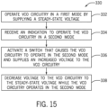
- FIG. 15 is a flowchart showing a method 330 to operate the switch control bootstrapping circuitry 260 of FIG. 13 to provide a bootstrap pulse 310, according to embodiments of the present disclosure.
- performing the method 330 of FIG. 15 may ensure that the desired mode of operation (e.g., Mode 1 208) of the VCO circuitry 67, 85 remains dominant over undesired modes of operation (e.g., Mode 0 194).
- Any suitable device e.g., a controller
- the method 330 may be implemented by executing instructions stored in a tangible, non-transitory, computer-readable medium, such as the memory 14 or storage 16, using the processor 12.
- the method 330 may be performed at least in part by one or more software components, such as an operating system of the electronic device 10, one or more software applications of the electronic device 10, and the like. While the method 330 is described using steps in a specific sequence, it should be understood that the present disclosure contemplates that the described steps may be performed in different sequences than the sequence illustrated, and certain described steps may be skipped or not performed altogether.
- the processor 12 initially operates the VCO circuitry 67, 85 in a first mode (e.g., Mode 0) by supplying a steady-state voltage (e.g., Vin-Vdrop).
- a steady-state voltage e.g., Vin-Vdrop
- the processor 12 may cause the VCO circuitry 67, 85 to operate in the first mode 294, and, as shown in the switch supply 282 diagram of FIG. 14 , supply the VCO circuitry 67, 85 with a steady-state supply voltage V in -V drop 296.
- the processor 12 receives an indication to operate the VCO circuitry 67, 85 in a second mode 308 (e.g., Mode 1). For example, it may be desired to generate a new or modify a current local oscillation signal 83, and operating the VCO circuitry 67, 85 in the second mode 208 may generate or facilitate generating the new or modified local oscillation signal 83.
- the processor 12 activates a switch (e.g., the switch 264 of the supply voltage switching circuitry 132 in the form of the switch control bootstrapping circuitry 260) that causes the VCO circuitry 67, 85 to operate in the second mode 308 and (e.g., concurrently, simultaneously, and/or instantaneously) supplies an increased voltage (e.g., the bootstrapping voltage V in 312) to the VCO circuitry 67, 85.
- a switch e.g., the switch 264 of the supply voltage switching circuitry 132 in the form of the switch control bootstrapping circuitry 260
- V in 312 the processor 12 causes the VCO circuitry 67, 85 to switch from operating in the first mode 294 to the second mode 308.
- the processor 12 also causes the switch control bootstrapping circuitry 260 to switch and supply a bootstrap pulse 312 (e.g., at voltage V in ) to bootstrap the second mode 308. Because the bootstrap pulse 310 (e.g., associated with switching to Mode 1 308) is at a greater voltage than the operating voltage of Mode 0 294 (e.g., prior to time t0 292), the loop gain 306 of Mode 1 308 increases or jumps up, while the loop gain 304 of Mode 0 294 decreases or drops down.
- a bootstrap pulse 312 e.g., at voltage V in
- the processor 12 supplies the steady-state voltage 316 (e.g., V in -V drop ) to the VCO circuitry 67, 85 while the VCO circuitry 67, 85 operates in the second mode 308.
- the processor 12 causes the switch control bootstrapping circuitry 260 to switch to the steady-state supply voltage V in -V drop 316.
- the VCO circuitry 67, 85 sustains stable oscillation at the second mode 308 (e.g., at frequency f1 318) as shown by the voltage waveform 286 diagram.
- the desired mode loop gain 306 of the desired second mode 308 decreases or drops down to a steady state and the undesired mode loop gain 304 of undesired first mode increases or jumps up to a steady state, while the desired mode loop gain 306 of second mode 1 308 is greater than and dominates the undesired mode loop gain 304 of undesired first mode 294, as shown by the mode loop gain 288 diagram.
- the method 330 enables the processor 12 to operate the switch control bootstrapping circuitry 260 to cause the VCO circuitry 67, 85 to operate in a desired operating mode 208 (e.g., Mode 1) and prevent or block undesired operating modes (e.g., Mode 0 194) from dominating the desired operating mode 208 using a bootstrap pulse 310.
- a desired operating mode 208 e.g., Mode 1
- undesired operating modes e.g., Mode 0 194
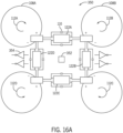
- FIG. 16A is an example implementation 350 of VCO circuitry 67, 85 having four cores 102A-D and the switching circuitry 122 of FIG. 7 as described herein operating in a first mode (e.g., Mode 0), according to an embodiment of the present disclosure.
- switching circuitry 122A-D is coupled in series between two cores 102, and capacitances 110 are coupled in parallel with the switching circuitry 122.
- the example implementation 350 of VCO circuitry 67, 85 also includes a mode detector 352 (e.g., mode detection circuitry) that detects a mode in which the VCO circuitry 67, 85 is currently operating.
- the mode detector 352 may be part of or coupled to the processor 12.
- VCO circuitry 67, 85 may include VCO buffers 354 (e.g., buffer amplifiers), which may facilitate isolating two circuit stages (e.g., one core 102 from another 102).
- Mode 0 may include each current direction 112A-D (collectively 112) in each inductor 108A-D (collectively 108) of each core 102 having an opposite current direction when compared to that of its adjacent cores 102.
- each core 102 may be in phase with its adjacent cores 102.
- a current direction 112A (e.g., clockwise) of a first inductor 108A of a first core 102A may be opposite to that of current directions 112B, 112D (e.g., counterclockwise) of second and fourth inductors 108B, 108D of adjacent second and fourth cores 102B, 102D.
- a current direction 112B (e.g., counterclockwise) of a second inductor 108B of a second core 102B may be opposite to that of current directions 112A, 112C (e.g., clockwise) of first and third inductors 108A, 108C of adjacent first and third cores 102A, 102C, and so on.
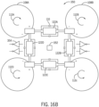
- FIG. 16B is the example implementation 350 of VCO circuitry 67, 85 of FIG. 16A operating in a second mode (e.g., Mode 1), according to an embodiment of the present disclosure.
- Mode 1 may include current directions 112 in two inductors 108 of adjacent cores 102 having a first current direction (e.g., as such, the two adjacent cores 102 are out-of-phase), and current directions 112 in two other inductors 108 of two other adjacent cores 102 having a second current direction different from the first current direction (e.g., as such, the two other adjacent cores 102 are out-of-phase).
- the current directions 112A, 112B e.g., clockwise
- the current directions 112C, 112D e.g., counterclockwise
- the third and fourth inductors 108C, 108D of adjacent third and fourth cores 102C, 102D are the same, but different from the current directions 112A, 112B of the first and second inductors 108A, 108B of the first and second cores 102A, 102B.
- the first core 102A is in phase with the fourth core 102D
- the second core 102B is in phase with the third core 102C
- the first core 102A is out of phase with the second core 102B
- the third core 102C is out of phase with the fourth core 102D.
- FIG. 16C is the example implementation 350 of VCO circuitry 67, 85 of FIG. 16A operating in a third mode (e.g., Mode 2), according to an embodiment of the present disclosure.
- Mode 2 may include current directions 112 in two inductors 108 of adjacent cores 102 having a first current direction (e.g., as such, the two adjacent cores 102 are out-of-phase), and current directions 112 in two other inductors 108 of two other adjacent cores 102 having a second current direction different from the first current direction (e.g., as such, the two other adjacent cores 102 are out-of-phase).
- the current directions 112A, 112D e.g., clockwise
- the current directions 112B, 112C e.g., counterclockwise
- the second and third inductors 108B, 108C of adjacent second and third cores 102B, 102C are the same, but different from the current directions 112A, 112D of the first and fourth inductors 108A, 108D of the first and fourth cores 102A, 102D.
- the first core 102A is in phase with the second core 102B
- the third core 102C is in phase with the fourth core 102D
- the first core 102A is out of phase with the fourth core 102D
- the second core 102B is out of phase with the third core 102C.
- FIG. 16D is the example implementation 350 of VCO circuitry 67, 85 of FIG. 16A operating in a fourth mode (e.g., Mode 3), according to an embodiment of the present disclosure.
- Mode 3 may include current directions 112 in all four inductors 108 of the cores 102 having the same current direction (e.g., as such, all four cores 102 are out-of-phase. That is, the current directions 112A-D (e.g., clockwise) of all four inductors 108A-D of all four cores 102A-D are the same. As such, all four cores 102A-D are out of phase with one another.
- the switching circuitry 122 may facilitate a desired mode to be dominant over undesired modes.
- the processor 12 may switch from an initial mode (e.g., Mode 0 194) to a desired mode (e.g., Mode 1 208) and the switch control reset and ramping circuitry 134 may switch from providing a steady-state supply voltage to providing a reset pulse 210 and a ramp pulse 214 that causes the desired mode to dominate over undesired operating modes and remain dominant over the undesired operating modes.
- an initial mode e.g., Mode 0 194
- a desired mode e.g., Mode 1 208
- the switch control reset and ramping circuitry 134 may switch from providing a steady-state supply voltage to providing a reset pulse 210 and a ramp pulse 214 that causes the desired mode to dominate over undesired operating modes and remain dominant over the undesired operating modes.
- the processor 12 may switch from the initial mode to the desired mode and the switch control bootstrapping circuitry 260 may switch from providing a steady-state supply voltage to providing a bootstrap pulse 312 that causes the desired mode to dominate over undesired operating modes and remain dominant over the undesired operating modes.
- VCO circuitry 67, 85 shown in FIGS. 16A-D is purely an example, and any suitable number of cores (e.g., more or less cores), components (e.g., more or less components), operating modes (e.g., more or less operating modes), and so on, are contemplated.
- the VCO circuitry 67, 85 may have any suitable (e.g., N) number of cores 102 and corresponding switching circuitry 122.
- FIG. 17 is a plot illustrating operation of VCO circuitry without the switching circuitry 122 illustrated in FIG. 7 .
- the plot includes a horizontal or x-axis 370 representing the different modes in which the VCO circuitry 67, 85 may operate (e.g., Mode 0, Mode 1, Mode 2, and Mode 3), and a vertical or y-axis 372 represents loop gain (e.g., in decibels).
- Modes 0-3 shown on the horizontal axis 370 correspond to the Modes shown in FIGS. 16A-D .
- Mode 2 is desired 374
- Modes 0, 1, and 3 are undesired 376.
- Mode 0 may surpass Mode 2 and become dominant, as Mode 2 may have larger capacitances 110 between its cores 102 that have same current direction and lower tank quality factor when compared with those of Mode 0. That is, the capacitances 110 between the out-of-phase cores (e.g., the first and fourth cores 102A, 102D and the second and third cores 102B, 102C) may be larger, causing a lower tank quality factor in the VCO circuitry 67, 85 when operating in Mode 2 compared to operating in Mode 0.
- the out-of-phase cores e.g., the first and fourth cores 102A, 102D and the second and third cores 102B, 102C
- FIG. 18 is a plot illustrating operation of the example implementation 350 of VCO circuitry 67, 85 of FIGS. 16A-D , according to an embodiment of the present disclosure.
- operating the switching circuitry 122 to increase gain (e.g., as indicated by the upward arrow) associated with desired Mode 2 374 and decreasing or weakening gain (e.g., as indicated by the downward arrows) associated with the undesired operating modes 376 may ensure that desired Mode 2 374 is dominant over (e.g., has a greater loop gain compared to) the undesired operating modes 376 (e.g., Modes 0, 1, and 3) and remains dominant (e.g., continues to have a greater loop gain compared to the undesired operating modes 376).
- the switch control reset and ramping circuitry 134 may switch from providing a steady-state supply voltage to providing a reset pulse 210 and a ramp pulse 214 that causes gain of desired Mode 1 374 to be greater than that of the undesired modes 376 and remain dominant over the undesired modes 376.
- the switch control bootstrapping circuitry 260 may switch from providing a steady-state supply voltage to providing a bootstrap pulse 312 that causes gain of desired Mode 2 374 to be greater than that of the undesired modes 376 and remain dominant over the undesired modes 376.
- personally identifiable information should follow privacy policies and practices that are generally recognized as meeting or exceeding industry or governmental requirements for maintaining the privacy of users.
- personally identifiable information data should be managed and handled so as to minimize risks of unintentional or unauthorized access or use, and the nature of authorized use should be clearly indicated to users.
Landscapes
- Engineering & Computer Science (AREA)
- Computer Networks & Wireless Communication (AREA)
- Signal Processing (AREA)
- Inductance-Capacitance Distribution Constants And Capacitance-Resistance Oscillators (AREA)
- Transceivers (AREA)
Applications Claiming Priority (2)
| Application Number | Priority Date | Filing Date | Title |
|---|---|---|---|
| US202163246778P | 2021-09-21 | 2021-09-21 | |
| US17/748,904 US11817823B2 (en) | 2021-09-21 | 2022-05-19 | Multi-core oscillator with transient supply voltage assisted mode switching |
Publications (1)
| Publication Number | Publication Date |
|---|---|
| EP4152601A1 true EP4152601A1 (de) | 2023-03-22 |
Family
ID=82899262
Family Applications (1)
| Application Number | Title | Priority Date | Filing Date |
|---|---|---|---|
| EP22190063.2A Pending EP4152601A1 (de) | 2021-09-21 | 2022-08-11 | Mehrkernoszillator mit transienter versorgungsspannungsunterstützter modusumschaltung |
Country Status (4)
| Country | Link |
|---|---|
| US (2) | US11817823B2 (de) |
| EP (1) | EP4152601A1 (de) |
| KR (2) | KR102852760B1 (de) |
| CN (1) | CN115842547A (de) |
Families Citing this family (1)
| Publication number | Priority date | Publication date | Assignee | Title |
|---|---|---|---|---|
| SG11202110122WA (en) * | 2019-03-18 | 2021-10-28 | Frederic Nabki | Ultra wideband (uwb) transmitter and receiver circuits |
Citations (2)
| Publication number | Priority date | Publication date | Assignee | Title |
|---|---|---|---|---|
| EP2634914A1 (de) * | 2012-03-02 | 2013-09-04 | Nxp B.V. | Oszillatorschaltung |
| US20200371545A1 (en) * | 2019-05-23 | 2020-11-26 | Qualcomm Incorporated | Multi-Mode Oscillation Circuitry with Stepping Control |
Family Cites Families (16)
| Publication number | Priority date | Publication date | Assignee | Title |
|---|---|---|---|---|
| US5568099A (en) * | 1995-09-27 | 1996-10-22 | Cirrus Logic, Inc. | High frequency differential VCO with common biased clipper |
| JP4561029B2 (ja) * | 2001-07-31 | 2010-10-13 | セイコーエプソン株式会社 | 発振回路およびこれを用いた電子機器 |
| US7151915B2 (en) * | 2001-09-26 | 2006-12-19 | Nokia Corporation | Dual mode voltage controlled oscillator having controllable bias modes and power consumption |
| US6924708B2 (en) * | 2002-09-11 | 2005-08-02 | Visteon Global Technologies, Inc. | Oscillator circuit having an expanded operating range |
| JP4127084B2 (ja) * | 2003-03-12 | 2008-07-30 | 株式会社デンソー | センサ装置 |
| US7126433B2 (en) * | 2004-03-16 | 2006-10-24 | Freescale Semiconductor, Inc. | Self-calibrating oscillator system |
| KR100760196B1 (ko) * | 2005-12-08 | 2007-09-20 | 한국전자통신연구원 | 적응성 부성 저항셀을 장착한 멀티밴드용 lc 공조전압제어발진기 |
| US7663446B1 (en) * | 2006-06-23 | 2010-02-16 | Marvell International Ltd. | Adjustable supply voltage in a voltage controlled oscillator (VCO) for wide range frequency coverage |
| JP2008053784A (ja) * | 2006-08-22 | 2008-03-06 | Toshiba Corp | 電圧制御発振器、電圧制御発振器用のバイアス装置、電圧制御発振器のバイアス調整プログラム |
| US7602260B1 (en) * | 2007-11-21 | 2009-10-13 | Altera Corporation | Programmable supply voltage regulator for oscillator |
| WO2015097657A2 (en) * | 2013-12-23 | 2015-07-02 | Marvell Israel (M.I.S.L) Ltd. | Apparatus and method for reacting to a change in supply voltage |
| US10425038B2 (en) | 2015-10-14 | 2019-09-24 | Mediatek Inc. | LC-tank oscillator having intrinsic low-pass filter |
| US10230379B2 (en) | 2016-05-04 | 2019-03-12 | Apple Inc. | Downshift techniques for oscillator with feedback loop |
| JP2017220716A (ja) * | 2016-06-03 | 2017-12-14 | シナプティクス・ジャパン合同会社 | 発振回路 |
| US10749470B2 (en) * | 2018-11-09 | 2020-08-18 | Microsemi Storage Solutions, Inc. | Method and apparatus for multimode wideband oscillator |
| US11012079B1 (en) | 2019-12-19 | 2021-05-18 | Bae Systems Information And Electronic Systems Integration Inc. | Continuous tuning of digitally switched voltage-controlled oscillator frequency bands |
-
2022
- 2022-05-19 US US17/748,904 patent/US11817823B2/en active Active
- 2022-08-11 EP EP22190063.2A patent/EP4152601A1/de active Pending
- 2022-08-29 KR KR1020220108505A patent/KR102852760B1/ko active Active
- 2022-08-31 CN CN202211054675.5A patent/CN115842547A/zh active Pending
- 2022-09-12 US US17/942,850 patent/US11909355B2/en active Active
-
2025
- 2025-08-26 KR KR1020250119466A patent/KR102896634B1/ko active Active
Patent Citations (2)
| Publication number | Priority date | Publication date | Assignee | Title |
|---|---|---|---|---|
| EP2634914A1 (de) * | 2012-03-02 | 2013-09-04 | Nxp B.V. | Oszillatorschaltung |
| US20200371545A1 (en) * | 2019-05-23 | 2020-11-26 | Qualcomm Incorporated | Multi-Mode Oscillation Circuitry with Stepping Control |
Non-Patent Citations (2)
| Title |
|---|
| EL-AASSAR OMAR ET AL: "Octave-Tuning Dual-Core Folded VCO Leveraging a Triple-Mode Switch-Less Tertiary Magnetic Loop", IEEE JOURNAL OF SOLID-STATE CIRCUITS, IEEE, USA, vol. 56, no. 5, 31 March 2021 (2021-03-31), pages 1475 - 1486, XP011851153, ISSN: 0018-9200, [retrieved on 20210422], DOI: 10.1109/JSSC.2021.3059442 * |
| GUANSHENG LI ET AL: "A Low-Phase-Noise Wide-Tuning-Range Oscillator Based on Resonant Mode Switching", IEEE JOURNAL OF SOLID-STATE CIRCUITS, IEEE, USA, vol. 47, no. 6, 30 June 2012 (2012-06-30), pages 1295 - 1308, XP011444801, ISSN: 0018-9200, DOI: 10.1109/JSSC.2012.2190185 * |
Also Published As
| Publication number | Publication date |
|---|---|
| KR20230042556A (ko) | 2023-03-28 |
| US11817823B2 (en) | 2023-11-14 |
| KR20250134554A (ko) | 2025-09-11 |
| CN115842547A (zh) | 2023-03-24 |
| US20230090770A1 (en) | 2023-03-23 |
| KR102896634B1 (ko) | 2025-12-08 |
| KR102852760B1 (ko) | 2025-08-29 |
| US11909355B2 (en) | 2024-02-20 |
| US20230091463A1 (en) | 2023-03-23 |
Similar Documents
| Publication | Publication Date | Title |
|---|---|---|
| US12095495B2 (en) | Phased array systems and methods with phase shifter | |
| KR102896634B1 (ko) | 과도 공급 전압 보조 모드 스위칭을 갖는 다중 코어 발진기 | |
| US20250125810A1 (en) | Systems and methods for improved charge pump phase-locked loop phase stability | |
| US20240348258A1 (en) | Digital-to-analog converter with hybrid coupler | |
| US20090091361A1 (en) | Frequency divider configuration | |
| US12074568B2 (en) | Multi-core oscillator with enhanced mode robustness | |
| US20230403016A1 (en) | Unlimited Bandwidth Shifting Systems and Methods of an All-Digital Phase Locked Loop | |
| US11990913B2 (en) | Systems and methods for providing a delay-locked loop with coarse tuning technique | |
| US12603663B2 (en) | Dual-band RF mixer chain using dual-band matching network and shared local oscillator | |
| US20240305318A1 (en) | Dual-connectivity mobile satellite communication | |
| US20240097715A1 (en) | Dual-band rf mixer chain using dual-band matching network and shared local oscillator | |
| US12489475B2 (en) | Systems and methods to reduce interference in a radio frequency device | |
| US11870473B1 (en) | Digital-to-analog converter with hybrid coupler | |
| US20250105808A1 (en) | Sampled-data receiver with chopper stabilization | |
| US20230055562A1 (en) | Multiphase signal generator | |
| CN117749166A (zh) | 用于提供具有粗调技术的延迟锁相环的系统和方法 |
Legal Events
| Date | Code | Title | Description |
|---|---|---|---|
| PUAI | Public reference made under article 153(3) epc to a published international application that has entered the european phase |
Free format text: ORIGINAL CODE: 0009012 |
|
| STAA | Information on the status of an ep patent application or granted ep patent |
Free format text: STATUS: REQUEST FOR EXAMINATION WAS MADE |
|
| 17P | Request for examination filed |
Effective date: 20220811 |
|
| AK | Designated contracting states |
Kind code of ref document: A1 Designated state(s): AL AT BE BG CH CY CZ DE DK EE ES FI FR GB GR HR HU IE IS IT LI LT LU LV MC MK MT NL NO PL PT RO RS SE SI SK SM TR |
|
| STAA | Information on the status of an ep patent application or granted ep patent |
Free format text: STATUS: EXAMINATION IS IN PROGRESS |
|
| 17Q | First examination report despatched |
Effective date: 20250414 |