EP4152392A1 - Semiconductor structure and manufacturing method therefor - Google Patents
Semiconductor structure and manufacturing method therefor Download PDFInfo
- Publication number
- EP4152392A1 EP4152392A1 EP22712490.6A EP22712490A EP4152392A1 EP 4152392 A1 EP4152392 A1 EP 4152392A1 EP 22712490 A EP22712490 A EP 22712490A EP 4152392 A1 EP4152392 A1 EP 4152392A1
- Authority
- EP
- European Patent Office
- Prior art keywords
- word line
- conductive layer
- layer
- single junction
- semiconductor structure
- Prior art date
- Legal status (The legal status is an assumption and is not a legal conclusion. Google has not performed a legal analysis and makes no representation as to the accuracy of the status listed.)
- Pending
Links
Images



Classifications
-
- H—ELECTRICITY
- H10—SEMICONDUCTOR DEVICES; ELECTRIC SOLID-STATE DEVICES NOT OTHERWISE PROVIDED FOR
- H10B—ELECTRONIC MEMORY DEVICES
- H10B12/00—Dynamic random access memory [DRAM] devices
- H10B12/30—DRAM devices comprising one-transistor - one-capacitor [1T-1C] memory cells
- H10B12/48—Data lines or contacts therefor
- H10B12/488—Word lines
-
- H—ELECTRICITY
- H10—SEMICONDUCTOR DEVICES; ELECTRIC SOLID-STATE DEVICES NOT OTHERWISE PROVIDED FOR
- H10B—ELECTRONIC MEMORY DEVICES
- H10B12/00—Dynamic random access memory [DRAM] devices
- H10B12/30—DRAM devices comprising one-transistor - one-capacitor [1T-1C] memory cells
-
- H—ELECTRICITY
- H10—SEMICONDUCTOR DEVICES; ELECTRIC SOLID-STATE DEVICES NOT OTHERWISE PROVIDED FOR
- H10B—ELECTRONIC MEMORY DEVICES
- H10B12/00—Dynamic random access memory [DRAM] devices
- H10B12/30—DRAM devices comprising one-transistor - one-capacitor [1T-1C] memory cells
- H10B12/31—DRAM devices comprising one-transistor - one-capacitor [1T-1C] memory cells having a storage electrode stacked over the transistor
-
- H—ELECTRICITY
- H10—SEMICONDUCTOR DEVICES; ELECTRIC SOLID-STATE DEVICES NOT OTHERWISE PROVIDED FOR
- H10D—INORGANIC ELECTRIC SEMICONDUCTOR DEVICES
- H10D62/00—Semiconductor bodies, or regions thereof, of devices having potential barriers
- H10D62/10—Shapes, relative sizes or dispositions of the regions of the semiconductor bodies; Shapes of the semiconductor bodies
- H10D62/13—Semiconductor regions connected to electrodes carrying current to be rectified, amplified or switched, e.g. source or drain regions
- H10D62/149—Source or drain regions of field-effect devices
-
- H—ELECTRICITY
- H10—SEMICONDUCTOR DEVICES; ELECTRIC SOLID-STATE DEVICES NOT OTHERWISE PROVIDED FOR
- H10D—INORGANIC ELECTRIC SEMICONDUCTOR DEVICES
- H10D64/00—Electrodes of devices having potential barriers
- H10D64/20—Electrodes characterised by their shapes, relative sizes or dispositions
- H10D64/27—Electrodes not carrying the current to be rectified, amplified, oscillated or switched, e.g. gates
- H10D64/311—Gate electrodes for field-effect devices
- H10D64/411—Gate electrodes for field-effect devices for FETs
- H10D64/511—Gate electrodes for field-effect devices for FETs for IGFETs
- H10D64/512—Disposition of the gate electrodes, e.g. buried gates
- H10D64/513—Disposition of the gate electrodes, e.g. buried gates within recesses in the substrate, e.g. trench gates, groove gates or buried gates
-
- H—ELECTRICITY
- H10—SEMICONDUCTOR DEVICES; ELECTRIC SOLID-STATE DEVICES NOT OTHERWISE PROVIDED FOR
- H10B—ELECTRONIC MEMORY DEVICES
- H10B12/00—Dynamic random access memory [DRAM] devices
- H10B12/01—Manufacture or treatment
- H10B12/02—Manufacture or treatment for one transistor one-capacitor [1T-1C] memory cells
- H10B12/05—Making the transistor
- H10B12/053—Making the transistor the transistor being at least partially in a trench in the substrate
-
- H—ELECTRICITY
- H10—SEMICONDUCTOR DEVICES; ELECTRIC SOLID-STATE DEVICES NOT OTHERWISE PROVIDED FOR
- H10B—ELECTRONIC MEMORY DEVICES
- H10B12/00—Dynamic random access memory [DRAM] devices
- H10B12/30—DRAM devices comprising one-transistor - one-capacitor [1T-1C] memory cells
- H10B12/34—DRAM devices comprising one-transistor - one-capacitor [1T-1C] memory cells the transistor being at least partially in a trench in the substrate
Definitions
- the disclosure relates to the technical field of semiconductors, in particular to a semiconductor structure and a manufacturing method thereof.
- DRAM Dynamic Random Access Memory
- Each memory cell usually includes a capacitor structure and a transistor.
- the gate of the transistor is composed of a word line, the drain of the transistor is connected to a bit line, and the source of the transistor is connected to the capacitor structure.
- a voltage signal on the word line can control the transistor to turn on or off, and then the data information stored in the capacitor structure can be read through the bit line, or the data information can be written into the capacitor structure through the bit line for storage.
- the gate of the transistor is composed of a word line, which is buried in a word line trench in a base including a P-type substrate and an N-type doped region located on the surface layer of the P-type substrate.
- the part of the P-type substrate close to the word line trench is used as the channel region of the transistor, and the N-type doped regions on both sides of the word line trench are the source region and the drain region of the transistor.
- the word line and the source/drain region are projected on a side wall of the word line trench respectively, the projected parts of the word line and the source/drain region form an overlapping region.
- the word line of the transistor is turned on, electrons may be attracted to the overlapping region. The larger the overlapping region is, the smaller the on-resistance of the source/drain region and the channel region are, and the larger the driving current of the transistor is.
- GIDL gate-induced drain leakage
- the embodiments of the disclosure provide a semiconductor structure and a manufacturing method thereof.
- the semiconductor structure can increase driving current of transistors and mitigate GIDL leakage phenomenon, thereby improving reliability of the semiconductor structure.
- the embodiments of the disclosure provide a semiconductor structure, which includes a substrate, with a plurality of word line trenches and source/drain regions each adjacent to each word line trench; a word line, located in each word line trench, and including a first conductive layer, a single junction layer and a second conductive layer stacked in sequence, in which the first conductive layer is located at a bottom of the word line trench, and the projection of the word line on a sidewall of the word line trench and the projection of the source/drain region on the sidewall of the word line trench have an overlapping region with a preset height, in which in the case that a voltage applied to the word line is less than a preset voltage, a resistance of the single junction layer is greater than a preset resistance, to make the first conductive layer and the second conductive layer disconnected.
- a projection of at least part of the second conductive layer on the sidewall of the word line trench is located within the projection of the source/drain region on the sidewall of the word line trench.
- a top of the first conductive layer is lower than a bottom of the source/drain region.
- a top of the second conductive layer is flush with a top of the source/drain region.
- the projection of the source/drain region on the sidewall of the word line trench covers a projection of the second conductive layer on the sidewall of the word line trench.
- the preset resistance is the critical resistance of electrical conduction of the first conductive layer and the second conductive layer.
- the single junction layer includes a first resistance and a second resistance, in which the first resistance is greater than the second resistance; in the case that the single junction layer is in a conductive state, the resistance of the single junction layer is the second resistance; and in the case that the single junction layer is in an off state, the resistance of the single junction layer is the first resistance.
- a conductive current of the single junction layer is 10 -4 A or more, and a conductive voltage is 1.2 V or more.
- the single junction layer is an OTS gating material layer.
- the single junction layer is a silicon telluride (SiTe) layer.
- the thickness of the single junction layer is 5 nm to 25 nm.
- the thickness of the single junction layer is 15 nm.
- the first conductive layer and/or the second conductive layer is a conductive metal layer.
- the first conductive layer and/or the second conductive layer is a tungsten (W) layer.
- the semiconductor structure provided by the embodiments of the disclosure has at least the following advantages.
- the word line includes a first conductive layer, a single junction layer and a second conductive layer stacked in sequence, in which the first conductive layer is located at the bottom of the word line trench.
- the single junction layer is in a conductive state
- the first conductive layer and the second conductive layer are connected through the single junction layer, and the overlapping region of the source/drain region and the word line can attract electrons of doped regions in the substrate, thereby reducing the resistance of the overlapping region of the source/drain region and the word line.
- the first conductive layer and the second conductive layer are disconnected, so the voltage of the second conductive layer is 0 V, and the second conductive layer can obviously reduce the electric field intensity of the overlapping region, and mitigate the phenomenon of forming a current due tp electrons tunneling between the word line and the source/drain, thereby mitigating the GIDL leakage phenomenon.
- the embodiments of the disclosure also provide a method for manufacturing a semiconductor structure, which includes: providing a substrate, on which a plurality of word line trenches and source/drain regions are formed, in which each source/drain region adjacent to each of the word line trench; forming a first conductive layer in each of the word line trench; forming a single junction layer on the first conductive layer; forming a second conductive layer on the single junction layer, in which the first conductive layer, the single junction layer and the second conductive layer form a word line, and a projection of the word line on a sidewall of the word line trench and a projections of the source/drain region on the sidewall of the word line trench have an overlapping region with a preset height.
- the dynamic random access memory in the related art has a serious problem of GIDL leakage.
- the reasons causing this problem are as follows. As shown in FIG. 1 , the distance from the top of a word line 200 to the upper surface of the substrate 100 (indicated by H in the embodiments of this disclosure) is reduced, and the overlapping region of the projections of the word line 200 and a source/drain region 102 on a sidewall of a word line trench 101 is increased (indicated by A in the embodiments of this disclosure).
- the overlapping region A can attract electrons in a doped region of the substrate 100, so as to reduce the resistance of the overlapping region A between the source/drain region 102 and the word line 200, thereby increasing driving current of the transistor.
- the electrons near to the overlapping region A can tunnel between the gate and the source/drain due to a strong electric field and thus form a current, i.e., GIDL leakage.
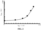
- FIG. 2 with the increase of the size of overlapping region A, the driving current increases, and the GIDL leakage phenomenon becomes more and more serious.
- a word line includes a first conductive layer, a single junction layer and a second conductive layer, which are sequentially stacked with the first conductive layer located at the bottom of the word line trench.
- the single junction layer is in a conductive state
- the first conductive layer and the second conductive layer are connected through the single junction layer, and the overlapping region A between the source/drain region and the word line can attract electrons in the doped regions of the substrate, thus reducing the resistance of the overlapping region A of the source/drain region and the word line, thereby increasing the driving current of the transistor.
- the second conductive layer can obviously reduce the electric field intensity in the overlapping region A, and thus mitigate the phenomenon of forming a current due to electrons tunneling between the word line and the source/drain, and mitigate the GIDL leakage phenomenon.
- FIG. 3 is a schematic structural diagram of a semiconductor structure provided by an embodiment of the disclosure
- FIG. 4 is a schematic diagram of a use state of a semiconductor structure provided by an embodiment of the disclosure
- FIG. 5 is a schematic diagram of a use state of the word line in FIG. 3
- FIG. 6 is a schematic diagram of another use state of the word line in FIG. 3 .
- the semiconductor structure provided by the embodiments of the disclosure includes a substrate 100 and a word line 200.
- the substrate 100 has several word line trenches 101 and source/drain regions 102, each of the source/drain region 102 is adjacent to each of the word line trench 101.
- the substrate 100 may be a crystalline semiconductor material, such as a silicon (Si) substrate 100, and the substrate 100 may also be a germanium (Ge) substrate 100, a silicon on insulator (SOI), a silicon germanium (SiGe) substrate 100, a silicon carbide (SiC) or gallium nitride (GaN) substrate 100, etc., for which the embodiments of the disclosure are not particularly limited.
- Si silicon
- Si silicon carbide
- GaN gallium nitride
- the substrate 100 includes a core region and a peripheral region located at the periphery of the core region.
- the core region includes multiple active areas and shallow trench isolation regions for isolating the active regions.
- the active regions can be arranged in an array.
- Capacitors are subsequently formed above the core area of the substrate 100, and peripheral circuits such as transistors are subsequently formed above the peripheral area of the substrate 100.
- a word line trench 101 is formed in each active area, and a semiconductor layer can be arranged in the substrate 100.
- the substrate 100 includes a P-type substrate 100 and an N-type doped region on the surface of the P-type substrate 100.
- the part of the P-type substrate 100 near the word line trench serves as the channel region of the transistor, and the N-type doped regions on both sides of the word line trench serve as a source region and a drain region of the transistor.
- the word line 200 is located in the word line trench 101.
- the word line 200 includes a first conductive layer 201, a single junction layer 202 and a second conductive layer 203 stacked in sequence.
- the first conductive layer 201 is located at the bottom of the word line trench 101.
- the projection of the word line 200 on the sidewall of the word line trench 101 and the projection of the source/drain region 102 on the sidewall of the word line trench 101 have an overlapping region A with a preset height.
- a voltage applied to the word line 200 is less than a preset voltage, the resistance of the single junction layer is greater than the preset resistance, so that the first conductive layer 201 and the second conductive layer 203 are disconnected.
- the resistance of the single junction layer 202 is less than a preset resistance, and the first conductive layer 201 and the second conductive layer 203 are connected through the single junction layer 202.
- the word line 200 in figure A of FIG. 5 is equivalent to the word line in figure B of FIG. 5 , and the heights of the overlapping region A of the projections of the word line 200 and the source/drain region 102 respectively on the sidewall of the word line trench are increased, thereby increasing the driving current.
- the resistance of the single junction layer 202 is greater than the preset resistance.
- the single junction layer 202 is in an off state, and the single junction layer 202 is used for breakoff of the first conductive layer 201 and the second conductive layer 203 so that the first conductive layer 201 and the second conductive layer 203 are disconnected.
- the word line 200 in figure C of FIG. 6 is equivalent to the word line of figure D of FIG. 6 .
- the second conductive layer 203 can shield the electric field of the first conductive layer 201, thereby reducing the electric field intensity of the overlapping region A of the projections of the word line 200 and the source/drain region 102 on the sidewall of the word line trench, and further mitigating the GIDL leakage phenomenon.
- the first conductive layer 201 and the second conductive layer 203 are connected through the single junction layer 202, and the overlapping region A of the source/drain region 102 and the word line 200 attract electrons in the doped region of the substrate 100, reducing the resistance of the overlapping region A of the source/drain region 102 and the word line 200, thereby increasing the driving current of the transistor.
- the first conductive layer 201 and the second conductive layer 203 are disconnected, so that the voltage on the second conductive layer 203 is 0 V, and the second conductive layer 203 can obviously reduce the electric field intensity in the overlapping region A, which mitigates the phenomenon of forming a current due to electrons tunneling between the word line 200 and the source/drain, and thus mitigate the GIDL leakage phenomenon.
- the height of the overlapping region A of the projections of the word line 200 and the source/drain region 102 on the sidewall of the word line trench is set for the purpose of increasing the driving current of transistors in the semiconductor structure, and the specific sizes are not specifically limited in this embodiment.
- the preset voltage can be 1.2V.
- the resistance of the single junction layer 202 is greater than the preset resistance, so that the first conductive layer 201 and the second conductive layer 203 are disconnected.
- the projection of at least part of the second conductive layer 203 on the sidewall of the word line trench 101 lies within the projection of the source/drain region 102 on the sidewall of the word line trench 101.
- the overlapping region A of the word line 200 and the source/drain region 102 includes at least part of the second conductive layer 203, so that when the single junction layer 202 is in the off state, the first conductive layer 201 and the second conductive layer 203 are disconnected, and the voltage of the second conductive layer 203 is 0 V.
- the second conductive layer 203 can shield the electric field near the first conductive layer 201, and thus mitigates the phenomenon of forming a current due to electrons tunneling between the word line 200 and the drain, thereby mitigating the GIDL leakage phenomenon.
- the top of the first conductive layer 201 is lower than the bottoms of the source/drain region 102.
- the overlapping region A of the word line 200 and the source/drain region 102 are composed of the second conductive layer 203, or the second conductive layer 203 and the single junction layer 202.
- the single junction layer 202 is in the off state, the distance between the electrons near the first conductive layer 201 and the source/drain region 102 is far.
- the second conductive layer 203 can shield the electric field near the first conductive layer 201, reducing the electric field intensity of the overlapping region A between the word line 200 and the source/drain region 102, and avoiding the current generated by electrons tunneling the source/drain region 102, so as to increase the driving current of the transistor and mitigate the GIDL leakage phenomenon.
- the top of the second conductive layer 203 is flush with the top of the source/drain region 102.
- the overlapping region A mainly includes the second conductive layer 203, so that when the single junction layer 202 is in the off state, the distance between the electrons near the first conductive layer 201 and the source/drain region 102 is far.
- the second conductive layer 203 can shield the electric field near the first conductive layer 201, reduce the electric field intensity in the overlapping region A of the word line 200 and the source/drain region 102, and avoid formation of the current due to electrons tunneling with the source/drain region 102, so as to increase the driving current of the transistor and mitigate the GIDL leakage phenomenon.
- the projection of the source/drain region 102 on the sidewall of the word line trench 101 covers the projection of the second conductive layer 203 on the sidewall of the word line trench 101, so that the GIDL leakage phenomenon can be mitigated while increasing the driving current of the transistor.
- the resistance of the single junction layer 202 is greater than the preset resistance, so that the first conductive layer 201 and the second conductive layer 203 are disconnected, in which the preset resistance is the critical resistance of electrical conduction of the first conductive layer 201 and the second conductive layer 203.
- the single junction layer 202 includes a first resistance and a second resistance, and the resistance value of the single junction layer 202 can vary between the first resistance and the second resistance under different voltages, in which the first resistance is greater than the second resistance.
- the resistance of the single junction layer 202 is the second resistance when the single junction layer 202 is in the conductive state.
- the resistance of the single junction layer 202 is the first resistance.
- the first resistance is a high-resistance state resistance, which is greater than the conductive resistance of the first conductive layer 201 and the second conductive layer 203, and thus the first conductive layer 201 and the second conductive layer 203 are disconnected through the single junction layer 202.
- the voltage of the second conductive layer 203 is 0 V, so that the second conductive layer 203 can be used for shielding the electric field of the word line 200.
- the second resistance is a low-resistance state resistance, which is less than the conductive resistance of the first conductive layer 201 and the second conductive layer 203, so that the first conductive layer 201 and the second conductive layer 203 can be connected through the single junction layer 202, so as to increase the height of the overlapping region A between the word line 200 and the source/drain region 102, thereby increasing the driving current of the transistor.
- the word line 200 when the voltage applied by the first conductive layer 201 is 3v, the single junction layer 202 is conductive in a low-resistance state.
- the word line 200 includes the first conductive layer 201, the single junction layer 202 and the second conductive layer 203, in which the first conductive layer 201 and the second conductive layer 203 are connected through the single junction layer 202 to increase the overlap region A between the word line 200 and the source/drain region 102.
- the voltage applied by the first conductive layer 201 is -0.2v, the single junction layer 202 is blocked by a high resistance state.
- the word line 200 includes the first conductive layer 201.
- the height of the overlapping region A between the word line 200 and the source/drain region 102 is reduced, and the second conductive layer 203 can also be used for shielding the electric field of the word line 200. Therefore the electric field strength of the overlapping region A of the word line 200 and the source/drain region 102 is reduced, and the GIDL leakage phenomenon is improved.
- FIG. 7 is a schematic diagram of the relationship between a voltage value and a resistance value of the single junction layer in on and off states of the embodiments of the disclosure.
- the conductive current of the single junction layer 202 is greater than or equal to 10 -4 A, and the conductive voltage is greater than or equal to 1.2V, so as to achieve the electrical conduction of the first conductive layer 201 and the second conductive layer 203 through the single junction layer 202; And when the voltage of the single junction layer 202 is greater than the preset voltage, the current increases significantly. Therefore, in order to meet the working reliability of the single junction layer 202, the single junction layer 202 can be made of a material with a high or a low resistance state as the voltage changes.
- the single junction layer 202 is an ovonic threshold switching (OTS) gating material layer.
- OTS ovonic threshold switching
- the single junction layer 202 may be a silicon telluride (SiTe) layer
- the first conductive layer 201 and the second conductive layer 203 may be conductive metal layers.
- the first conductive layer 201 and the second conductive layer 203 are tungsten (W) layers.
- the thickness of the single junction layer 202 may be 5 nm to 25 nm, in which the resistance value of the single junction layer 202 varies with the thickness of the single junction layer 202.
- the resistance value of the single junction layer 202 in the off state can be 6 times the resistance value of the single junction layer 202 in the connective state. As shown in FIG. 7 , the current value changes from 10 -10 A to 10 -4 A.
- the word line includes a first conductive layer, a single junction layer and a second conductive layer sequentially stacked, in which the first conductive layer is located at the bottom of the word line trench.
- the first conductive layer and the second conductive layer are connected through the single junction layer, and the overlapping region A between the source/drain region and the word line can attract electrons of the substrate doped region, thereby reducing the resistance of the overlapping region A between the source/drain region and the word line.
- the single junction layer is in an off state, the first conductive layer and the second conductive layer are disconnected, so that the voltage of the second conductive layer is 0 V.
- the second conductive layer can reduce the electric field intensity in the overlapping region A, and mitigate the phenomenon of forming the current due to electrons tunneling between the word line and the source/drain, thereby mitigating the GIDL leakage phenomenon.
- FIG. 8 is a flow diagram of a method for manufacturing a semiconductor structure provided by the embodiments of the disclosure.
- the embodiments of the disclosure also provide a method for manufacturing a semiconductor structure, which includes the following operations.
- a substrate is provided, and multiple word line trenches and source/drain regions are formed on the substrate, in which each of the source/drain regions adjacent to each of the word line trenches.
- a first conductive layer is formed in each word line trench.
- a single junction layer is formed on the first conductive layer.
- a second conductive layer on the single junction layer is formed, in which the first conductive layer, the single junction layer and the second conductive layer form a word line, and the projection of the word line on a sidewall of the word line trench and the projection of the source/drain region on the sidewall of the word line trench have an overlapping region with a preset height.
- a resistance of the single junction layer is greater than a preset resistance, and the single junction layer is in an off state.
- the single junction layer is used for blocking the first conductive layer and the second conductive layer, so that the first conductive layer and the second conductive layer are disconnected.
- the voltage applied by the single junction layer is greater than the preset voltage, the resistance of the single junction layer is less than the preset resistance, and the single junction layer is in a conductive state, and the single junction layer is used for connection of the first conductive layer and the second conductive layer.
- the method for manufacturing the semiconductor structure includes: providing a substrate, and forming a plurality of word line trenches and source/drain regions on the substrate, in which each of the source/drain regions is adjacent to each of the word line trenches; forming a first conductive layer in each of the word line trench; forming a single junction layer on the first conductive layer; a second conductive layer is formed on the single junction layer, and the first conductive layer, the single junction layer and the second conductive layer form a word line, in which the first conductive layer is located at the bottom of the word line trench; in which when the single junction layer is in a conductive state, the first conductive layer and the second conductive layer are connected through the single junction layer, and the overlapping region of the source/drain region and the word line attract electrons in the doped region of the substrate, thereby reducing the resistance of the overlapping region of the source/drain region and the word line, thereby increasing the driving current of the transistor.
- the first conductive layer and the second conductive layer are disconnected, so that the voltage of the second conductive layer is 0 V, and the second conductive layer reduces the electric field intensity in the overlapping region, thus mitigates the phenomenon of forming a current due to electrons tunneling between the word line and the source/drain, thereby mitigating the GIDL leakage phenomenon.
- each embodiment or implementation is described in a progressive manner, and each embodiment focuses on the differences from other embodiments, so it is enough to refer to the same and similar parts between each embodiment.
Landscapes
- Engineering & Computer Science (AREA)
- Manufacturing & Machinery (AREA)
- Semiconductor Memories (AREA)
- Insulated Gate Type Field-Effect Transistor (AREA)
Abstract
Description
- The present application claims priority to
Chinese Patent Application No. 202110904551.0 filed on August 06, 2021 - The disclosure relates to the technical field of semiconductors, in particular to a semiconductor structure and a manufacturing method thereof.
- Dynamic Random Access Memory (DRAM) is composed of multiple repeated memory cells. Each memory cell usually includes a capacitor structure and a transistor. The gate of the transistor is composed of a word line, the drain of the transistor is connected to a bit line, and the source of the transistor is connected to the capacitor structure. A voltage signal on the word line can control the transistor to turn on or off, and then the data information stored in the capacitor structure can be read through the bit line, or the data information can be written into the capacitor structure through the bit line for storage.
- In the related art, the gate of the transistor is composed of a word line, which is buried in a word line trench in a base including a P-type substrate and an N-type doped region located on the surface layer of the P-type substrate. The part of the P-type substrate close to the word line trench is used as the channel region of the transistor, and the N-type doped regions on both sides of the word line trench are the source region and the drain region of the transistor. When the word line and the source/drain region are projected on a side wall of the word line trench respectively, the projected parts of the word line and the source/drain region form an overlapping region. When the word line of the transistor is turned on, electrons may be attracted to the overlapping region. The larger the overlapping region is, the smaller the on-resistance of the source/drain region and the channel region are, and the larger the driving current of the transistor is.
- However, when the word line of the transistor is turned off, a strong electric field is formed in the overlapping region to attract tunneling current. The larger the overlapping region is, the more serious the phenomenon of gate-induced drain leakage (GIDL) is.
- In view of the above problems, the embodiments of the disclosure provide a semiconductor structure and a manufacturing method thereof. The semiconductor structure can increase driving current of transistors and mitigate GIDL leakage phenomenon, thereby improving reliability of the semiconductor structure.
- In order to achieve the above objectives, the embodiments of the disclosure provide the following technical solutions.
- The embodiments of the disclosure provide a semiconductor structure, which includes a substrate, with a plurality of word line trenches and source/drain regions each adjacent to each word line trench; a word line, located in each word line trench, and including a first conductive layer, a single junction layer and a second conductive layer stacked in sequence, in which the first conductive layer is located at a bottom of the word line trench, and the projection of the word line on a sidewall of the word line trench and the projection of the source/drain region on the sidewall of the word line trench have an overlapping region with a preset height, in which in the case that a voltage applied to the word line is less than a preset voltage, a resistance of the single junction layer is greater than a preset resistance, to make the first conductive layer and the second conductive layer disconnected.
- In the semiconductor structure as described above, a projection of at least part of the second conductive layer on the sidewall of the word line trench is located within the projection of the source/drain region on the sidewall of the word line trench.
- In the semiconductor structure as described above, a top of the first conductive layer is lower than a bottom of the source/drain region.
- In the semiconductor structure as described above, a top of the second conductive layer is flush with a top of the source/drain region.
- In the semiconductor structure as described above, the projection of the source/drain region on the sidewall of the word line trench covers a projection of the second conductive layer on the sidewall of the word line trench.
- In the semiconductor structure as described above, the preset resistance is the critical resistance of electrical conduction of the first conductive layer and the second conductive layer.
- In the semiconductor structure as described above, the single junction layer includes a first resistance and a second resistance, in which the first resistance is greater than the second resistance; in the case that the single junction layer is in a conductive state, the resistance of the single junction layer is the second resistance; and in the case that the single junction layer is in an off state, the resistance of the single junction layer is the first resistance.
- In the semiconductor structure as described above, a conductive current of the single junction layer is 10-4 A or more, and a conductive voltage is 1.2 V or more.
- In the semiconductor structure as described above, the single junction layer is an OTS gating material layer.
- In the semiconductor structure as described above, the single junction layer is a silicon telluride (SiTe) layer.
- In the semiconductor structure as described above, the thickness of the single junction layer is 5 nm to 25 nm.
- In the semiconductor structure as described above, the thickness of the single junction layer is 15 nm.
- In the semiconductor structure as described above, the first conductive layer and/or the second conductive layer is a conductive metal layer.
- In the semiconductor structure as described above, the first conductive layer and/or the second conductive layer is a tungsten (W) layer.
- The semiconductor structure provided by the embodiments of the disclosure has at least the following advantages.
- According to the semiconductor structure provided by the embodiments of the disclosure, the word line includes a first conductive layer, a single junction layer and a second conductive layer stacked in sequence, in which the first conductive layer is located at the bottom of the word line trench. In the case that the single junction layer is in a conductive state, the first conductive layer and the second conductive layer are connected through the single junction layer, and the overlapping region of the source/drain region and the word line can attract electrons of doped regions in the substrate, thereby reducing the resistance of the overlapping region of the source/drain region and the word line. However, in the case that the single junction layer is in an off state, the first conductive layer and the second conductive layer are disconnected, so the voltage of the second conductive layer is 0 V, and the second conductive layer can obviously reduce the electric field intensity of the overlapping region, and mitigate the phenomenon of forming a current due tp electrons tunneling between the word line and the source/drain, thereby mitigating the GIDL leakage phenomenon.
- The embodiments of the disclosure also provide a method for manufacturing a semiconductor structure, which includes: providing a substrate, on which a plurality of word line trenches and source/drain regions are formed, in which each source/drain region adjacent to each of the word line trench; forming a first conductive layer in each of the word line trench; forming a single junction layer on the first conductive layer; forming a second conductive layer on the single junction layer, in which the first conductive layer, the single junction layer and the second conductive layer form a word line, and a projection of the word line on a sidewall of the word line trench and a projections of the source/drain region on the sidewall of the word line trench have an overlapping region with a preset height.
- In addition to the technical problems solved by the embodiments of the disclosure, the technical features constituting the technical solutions and the beneficial effects brought by the technical features of these technical solutions described above, other technical problems that can be solved by the semiconductor structure and its manufacturing method provided by the embodiments of the disclosure, other technical features contained in the technical solutions and the beneficial effects brought by these technical features are further explained in detail in the specific implementation.
- In order to more clearly explain the embodiments of the disclosure or the technical solutions in the relate art, the following will briefly introduce the drawings that need to be used in the description of the embodiments or the related art. Obviously, the drawings in the following description are some embodiments of the disclosure, and for ordinary technicians in the field, other drawings can be obtained according to these drawings without involving creative efforts.
-
FIG. 1 is a structural diagram of a semiconductor structure in the related art; -
FIG. 2 is a schematic diagram of the relationship between the driving current and GIDL leakage after increasing the height of the overlap region between the word line and the source/drain region in the semiconductor structure; -
FIG. 3 is a schematic structural diagram of a semiconductor structure provided by an embodiment of the disclosure; -
FIG. 4 is a schematic diagram of a use state of a semiconductor structure provided by an embodiment of the disclosure; -
FIG. 5 is a schematic diagram of a use state of the word line inFIG. 3 ; -
FIG. 6 is a schematic diagram of another use state of the word line inFIG. 3 ; -
FIG. 7 is a schematic diagram of the relationship between the voltage value and the resistance value of the single junction layer in the on and off states provided by the embodiment of the disclosure; and -
FIG. 8 is a flow diagram of a method for manufacturing method a semiconductor structure provided by an embodiment of the disclosure. -
- 100- substrate;
- 101- word line trench;
- 102-source/drain region;
- 200-word line;
- 201- first conductive layer;
- 202- single junction layer;
- 203- second conductive layer.
- As mentioned in the background, the dynamic random access memory in the related art has a serious problem of GIDL leakage. According to the inventor's research, the reasons causing this problem are as follows. As shown in
FIG. 1 , the distance from the top of aword line 200 to the upper surface of the substrate 100 (indicated by H in the embodiments of this disclosure) is reduced, and the overlapping region of the projections of theword line 200 and a source/drain region 102 on a sidewall of aword line trench 101 is increased (indicated by A in the embodiments of this disclosure). When theword line 200 is turned on, the overlapping region A can attract electrons in a doped region of thesubstrate 100, so as to reduce the resistance of the overlapping region A between the source/drain region 102 and theword line 200, thereby increasing driving current of the transistor. - However, when the word line is in an off state and a working voltage is applied to the source and drain, the electrons near to the overlapping region A can tunnel between the gate and the source/drain due to a strong electric field and thus form a current, i.e., GIDL leakage. The larger the size of the overlapping region A is, the more serious the GIDL leakage phenomenon is, leading to a low reliability of the semiconductor structure. As shown in
FIG. 2 , with the increase of the size of overlapping region A, the driving current increases, and the GIDL leakage phenomenon becomes more and more serious. - In order to solve the above problem, the embodiments of the disclosure provide a semiconductor structure and its manufacturing method. In the semiconductor structure, a word line includes a first conductive layer, a single junction layer and a second conductive layer, which are sequentially stacked with the first conductive layer located at the bottom of the word line trench. When the single junction layer is in a conductive state, the first conductive layer and the second conductive layer are connected through the single junction layer, and the overlapping region A between the source/drain region and the word line can attract electrons in the doped regions of the substrate, thus reducing the resistance of the overlapping region A of the source/drain region and the word line, thereby increasing the driving current of the transistor. While when the single junction layer is in an off state, the first conductive layer and the second conductive layer are disconnected, so that the voltage on the second conductive layer is 0 V. Therefore, the second conductive layer can obviously reduce the electric field intensity in the overlapping region A, and thus mitigate the phenomenon of forming a current due to electrons tunneling between the word line and the source/drain, and mitigate the GIDL leakage phenomenon.
- In order to make the above-mentioned objects, features and advantages of the embodiments of the disclosure more obvious and understandable, the technical solutions in the embodiments of the disclosure are clearly and completely described below with reference to the drawings in the embodiments of the disclosure. It is apparent that, the described embodiments are only part of the embodiments of the disclosure, not all of them. Based on the embodiments in this disclosure, all other embodiments obtained by one of ordinary skill in the art without involving creative efforts are within the protection scope of in this disclosure.
-
FIG. 3 is a schematic structural diagram of a semiconductor structure provided by an embodiment of the disclosure;FIG. 4 is a schematic diagram of a use state of a semiconductor structure provided by an embodiment of the disclosure;FIG. 5 is a schematic diagram of a use state of the word line inFIG. 3 ; andFIG. 6 is a schematic diagram of another use state of the word line inFIG. 3 . - As shown in
FIGs. 3 to 6 , the semiconductor structure provided by the embodiments of the disclosure includes asubstrate 100 and aword line 200. - In the semiconductor structure, the
substrate 100 has severalword line trenches 101 and source/drain regions 102, each of the source/drain region 102 is adjacent to each of theword line trench 101. - The
substrate 100 may be a crystalline semiconductor material, such as a silicon (Si)substrate 100, and thesubstrate 100 may also be a germanium (Ge)substrate 100, a silicon on insulator (SOI), a silicon germanium (SiGe)substrate 100, a silicon carbide (SiC) or gallium nitride (GaN)substrate 100, etc., for which the embodiments of the disclosure are not particularly limited. - The
substrate 100 includes a core region and a peripheral region located at the periphery of the core region. The core region includes multiple active areas and shallow trench isolation regions for isolating the active regions. The active regions can be arranged in an array. - Capacitors are subsequently formed above the core area of the
substrate 100, and peripheral circuits such as transistors are subsequently formed above the peripheral area of thesubstrate 100. - A
word line trench 101 is formed in each active area, and a semiconductor layer can be arranged in thesubstrate 100. For example, thesubstrate 100 includes a P-type substrate 100 and an N-type doped region on the surface of the P-type substrate 100. The part of the P-type substrate 100 near the word line trench serves as the channel region of the transistor, and the N-type doped regions on both sides of the word line trench serve as a source region and a drain region of the transistor. - The
word line 200 is located in theword line trench 101. Theword line 200 includes a firstconductive layer 201, asingle junction layer 202 and a secondconductive layer 203 stacked in sequence. The firstconductive layer 201 is located at the bottom of theword line trench 101. The projection of theword line 200 on the sidewall of theword line trench 101 and the projection of the source/drain region 102 on the sidewall of theword line trench 101 have an overlapping region A with a preset height. When a voltage applied to theword line 200 is less than a preset voltage, the resistance of the single junction layer is greater than the preset resistance, so that the firstconductive layer 201 and the secondconductive layer 203 are disconnected. - It can be understood that, as shown in
FIGs. 3 and5 , when the voltage applied to theword line 200 is greater than the preset voltage, the resistance of thesingle junction layer 202 is less than a preset resistance, and the firstconductive layer 201 and the secondconductive layer 203 are connected through thesingle junction layer 202. In the case, theword line 200 in figure A ofFIG. 5 is equivalent to the word line in figure B ofFIG. 5 , and the heights of the overlapping region A of the projections of theword line 200 and the source/drain region 102 respectively on the sidewall of the word line trench are increased, thereby increasing the driving current. When the voltage applied to theword line 200 is less than the preset voltage, the resistance of thesingle junction layer 202 is greater than the preset resistance. As shown inFIG. 4 andFIG. 6 , thesingle junction layer 202 is in an off state, and thesingle junction layer 202 is used for breakoff of the firstconductive layer 201 and the secondconductive layer 203 so that the firstconductive layer 201 and the secondconductive layer 203 are disconnected. In the case, theword line 200 in figure C ofFIG. 6 is equivalent to the word line of figure D ofFIG. 6 . The secondconductive layer 203 can shield the electric field of the firstconductive layer 201, thereby reducing the electric field intensity of the overlapping region A of the projections of theword line 200 and the source/drain region 102 on the sidewall of the word line trench, and further mitigating the GIDL leakage phenomenon. - In the disclosure, when the
single junction layer 202 is in the conductive state, the firstconductive layer 201 and the secondconductive layer 203 are connected through thesingle junction layer 202, and the overlapping region A of the source/drain region 102 and theword line 200 attract electrons in the doped region of thesubstrate 100, reducing the resistance of the overlapping region A of the source/drain region 102 and theword line 200, thereby increasing the driving current of the transistor. While, when thesingle junction layer 202 is in the off state, the firstconductive layer 201 and the secondconductive layer 203 are disconnected, so that the voltage on the secondconductive layer 203 is 0 V, and the secondconductive layer 203 can obviously reduce the electric field intensity in the overlapping region A, which mitigates the phenomenon of forming a current due to electrons tunneling between theword line 200 and the source/drain, and thus mitigate the GIDL leakage phenomenon. - It should be noted that the height of the overlapping region A of the projections of the
word line 200 and the source/drain region 102 on the sidewall of the word line trench is set for the purpose of increasing the driving current of transistors in the semiconductor structure, and the specific sizes are not specifically limited in this embodiment. - In the semiconductor structure, the preset voltage can be 1.2V. When the voltage applied by the
word line 200 is less than 1.2V, the resistance of thesingle junction layer 202 is greater than the preset resistance, so that the firstconductive layer 201 and the secondconductive layer 203 are disconnected. - In some alternative embodiments, the projection of at least part of the second
conductive layer 203 on the sidewall of theword line trench 101 lies within the projection of the source/drain region 102 on the sidewall of theword line trench 101. - It can be understood that at least part of the second
conductive layer 203 refers to part of the secondconductive layer 203 or the whole conductive layer. The overlapping region A of theword line 200 and the source/drain region 102 includes at least part of the secondconductive layer 203, so that when thesingle junction layer 202 is in the off state, the firstconductive layer 201 and the secondconductive layer 203 are disconnected, and the voltage of the secondconductive layer 203 is 0 V. The secondconductive layer 203 can shield the electric field near the firstconductive layer 201, and thus mitigates the phenomenon of forming a current due to electrons tunneling between theword line 200 and the drain, thereby mitigating the GIDL leakage phenomenon. - Further, the top of the first
conductive layer 201 is lower than the bottoms of the source/drain region 102. - It can be understood that by setting the top of the first
conductive layer 201 to be lower than the bottom of the source/drain region 102, the overlapping region A of theword line 200 and the source/drain region 102 are composed of the secondconductive layer 203, or the secondconductive layer 203 and thesingle junction layer 202. When thesingle junction layer 202 is in the off state, the distance between the electrons near the firstconductive layer 201 and the source/drain region 102 is far. Furthermore, the secondconductive layer 203 can shield the electric field near the firstconductive layer 201, reducing the electric field intensity of the overlapping region A between theword line 200 and the source/drain region 102, and avoiding the current generated by electrons tunneling the source/drain region 102, so as to increase the driving current of the transistor and mitigate the GIDL leakage phenomenon. - Further, the top of the second
conductive layer 203 is flush with the top of the source/drain region 102. - By setting the top of the second
conductive layer 203 to be flush with the top of the source/drain region 102, the height of the overlapping region A of theword line 200 and the source/drain region 102 can be increased, thereby increasing the driving current of the transistor. Meanwhile, the overlapping region A mainly includes the secondconductive layer 203, so that when thesingle junction layer 202 is in the off state, the distance between the electrons near the firstconductive layer 201 and the source/drain region 102 is far. The secondconductive layer 203 can shield the electric field near the firstconductive layer 201, reduce the electric field intensity in the overlapping region A of theword line 200 and the source/drain region 102, and avoid formation of the current due to electrons tunneling with the source/drain region 102, so as to increase the driving current of the transistor and mitigate the GIDL leakage phenomenon. - In other alternative embodiments, the projection of the source/
drain region 102 on the sidewall of theword line trench 101 covers the projection of the secondconductive layer 203 on the sidewall of theword line trench 101, so that the GIDL leakage phenomenon can be mitigated while increasing the driving current of the transistor. - On the basis of the above embodiments, when the voltage applied to the
word line 200 is less than the preset voltage, the resistance of thesingle junction layer 202 is greater than the preset resistance, so that the firstconductive layer 201 and the secondconductive layer 203 are disconnected, in which the preset resistance is the critical resistance of electrical conduction of the firstconductive layer 201 and the secondconductive layer 203. - In the embodiments of the disclosure, the
single junction layer 202 includes a first resistance and a second resistance, and the resistance value of thesingle junction layer 202 can vary between the first resistance and the second resistance under different voltages, in which the first resistance is greater than the second resistance. The resistance of thesingle junction layer 202 is the second resistance when thesingle junction layer 202 is in the conductive state. When thesingle junction layer 202 is in the off state, the resistance of thesingle junction layer 202 is the first resistance. - It can be understood that when the voltage applied to the
word line 200 is less than the preset voltage, the first resistance is a high-resistance state resistance, which is greater than the conductive resistance of the firstconductive layer 201 and the secondconductive layer 203, and thus the firstconductive layer 201 and the secondconductive layer 203 are disconnected through thesingle junction layer 202. In this case, the voltage of the secondconductive layer 203 is 0 V, so that the secondconductive layer 203 can be used for shielding the electric field of theword line 200. When the voltage applied to theword line 200 is greater than the preset voltage, the second resistance is a low-resistance state resistance, which is less than the conductive resistance of the firstconductive layer 201 and the secondconductive layer 203, so that the firstconductive layer 201 and the secondconductive layer 203 can be connected through thesingle junction layer 202, so as to increase the height of the overlapping region A between theword line 200 and the source/drain region 102, thereby increasing the driving current of the transistor. - Illustratively, when the voltage applied by the first
conductive layer 201 is 3v, thesingle junction layer 202 is conductive in a low-resistance state. In this case, theword line 200 includes the firstconductive layer 201, thesingle junction layer 202 and the secondconductive layer 203, in which the firstconductive layer 201 and the secondconductive layer 203 are connected through thesingle junction layer 202 to increase the overlap region A between theword line 200 and the source/drain region 102. When the voltage applied by the firstconductive layer 201 is -0.2v, thesingle junction layer 202 is blocked by a high resistance state. In this case, theword line 200 includes the firstconductive layer 201. The height of the overlapping region A between theword line 200 and the source/drain region 102 is reduced, and the secondconductive layer 203 can also be used for shielding the electric field of theword line 200. Therefore the electric field strength of the overlapping region A of theword line 200 and the source/drain region 102 is reduced, and the GIDL leakage phenomenon is improved. -
FIG. 7 is a schematic diagram of the relationship between a voltage value and a resistance value of the single junction layer in on and off states of the embodiments of the disclosure. - Furthermore, it can be seen from
FIG. 7 that the conductive current of thesingle junction layer 202 is greater than or equal to 10-4 A, and the conductive voltage is greater than or equal to 1.2V, so as to achieve the electrical conduction of the firstconductive layer 201 and the secondconductive layer 203 through thesingle junction layer 202; And when the voltage of thesingle junction layer 202 is greater than the preset voltage, the current increases significantly. Therefore, in order to meet the working reliability of thesingle junction layer 202, thesingle junction layer 202 can be made of a material with a high or a low resistance state as the voltage changes. - In the semiconductor structure, the
single junction layer 202 is an ovonic threshold switching (OTS) gating material layer. - Illustratively, the
single junction layer 202 may be a silicon telluride (SiTe) layer, and the firstconductive layer 201 and the secondconductive layer 203 may be conductive metal layers. For example, the firstconductive layer 201 and the secondconductive layer 203 are tungsten (W) layers. - Further, the thickness of the
single junction layer 202 may be 5 nm to 25 nm, in which the resistance value of thesingle junction layer 202 varies with the thickness of thesingle junction layer 202. - Illustratively, when the
single junction layer 202 is a 15nm SiTe layer, and the firstconductive layer 201 and the secondconductive layer 203 are tungsten layers, the resistance value of thesingle junction layer 202 in the off state can be 6 times the resistance value of thesingle junction layer 202 in the connective state. As shown inFIG. 7 , the current value changes from 10-10 A to 10-4 A. - According to the semiconductor structure provided by the embodiments of the disclosure, the word line includes a first conductive layer, a single junction layer and a second conductive layer sequentially stacked, in which the first conductive layer is located at the bottom of the word line trench. When the single junction layer is in a conductive state, the first conductive layer and the second conductive layer are connected through the single junction layer, and the overlapping region A between the source/drain region and the word line can attract electrons of the substrate doped region, thereby reducing the resistance of the overlapping region A between the source/drain region and the word line. However, when the single junction layer is in an off state, the first conductive layer and the second conductive layer are disconnected, so that the voltage of the second conductive layer is 0 V. The second conductive layer can reduce the electric field intensity in the overlapping region A, and mitigate the phenomenon of forming the current due to electrons tunneling between the word line and the source/drain, thereby mitigating the GIDL leakage phenomenon.
-
FIG. 8 is a flow diagram of a method for manufacturing a semiconductor structure provided by the embodiments of the disclosure. - As shown in
FIG. 8 , the embodiments of the disclosure also provide a method for manufacturing a semiconductor structure, which includes the following operations. - At S101: a substrate is provided, and multiple word line trenches and source/drain regions are formed on the substrate, in which each of the source/drain regions adjacent to each of the word line trenches.
- At S 102: a first conductive layer is formed in each word line trench.
- At S103: a single junction layer is formed on the first conductive layer.
- At S 104: a second conductive layer on the single junction layer is formed, in which the first conductive layer, the single junction layer and the second conductive layer form a word line, and the projection of the word line on a sidewall of the word line trench and the projection of the source/drain region on the sidewall of the word line trench have an overlapping region with a preset height.
- In the semiconductor structure, when a voltage applied to the word line is less than a preset voltage, a resistance of the single junction layer is greater than a preset resistance, and the single junction layer is in an off state. The single junction layer is used for blocking the first conductive layer and the second conductive layer, so that the first conductive layer and the second conductive layer are disconnected. When the voltage applied by the single junction layer is greater than the preset voltage, the resistance of the single junction layer is less than the preset resistance, and the single junction layer is in a conductive state, and the single junction layer is used for connection of the first conductive layer and the second conductive layer.
- The method for manufacturing the semiconductor structure provided by embodiments of the disclosure includes: providing a substrate, and forming a plurality of word line trenches and source/drain regions on the substrate, in which each of the source/drain regions is adjacent to each of the word line trenches; forming a first conductive layer in each of the word line trench; forming a single junction layer on the first conductive layer; a second conductive layer is formed on the single junction layer, and the first conductive layer, the single junction layer and the second conductive layer form a word line, in which the first conductive layer is located at the bottom of the word line trench; in which when the single junction layer is in a conductive state, the first conductive layer and the second conductive layer are connected through the single junction layer, and the overlapping region of the source/drain region and the word line attract electrons in the doped region of the substrate, thereby reducing the resistance of the overlapping region of the source/drain region and the word line, thereby increasing the driving current of the transistor. While, when the single junction layer is in an off state, the first conductive layer and the second conductive layer are disconnected, so that the voltage of the second conductive layer is 0 V, and the second conductive layer reduces the electric field intensity in the overlapping region, thus mitigates the phenomenon of forming a current due to electrons tunneling between the word line and the source/drain, thereby mitigating the GIDL leakage phenomenon.
- In this description, each embodiment or implementation is described in a progressive manner, and each embodiment focuses on the differences from other embodiments, so it is enough to refer to the same and similar parts between each embodiment.
- In the description of this specification, referring to the description of the terms "one embodiment", "some embodiments", "illustrative embodiments", "examples", "concrete examples" or "some examples" means that the specific features, structures, materials or characteristics described in connection with the embodiments or examples are included in at least one embodiment or example of the disclosure. In this specification, the schematic expressions of the above terms do not necessarily refer to the same embodiments or examples. Furthermore, the specific features, structures, materials or characteristics described may be combined in any one or more embodiments or examples in a suitable manner.
- Finally, it should be noted that the above embodiments are only used for illustrating the technical solutions of the disclosure, but not to limit it; although the disclosure has been described in detail with reference to the foregoing embodiments, ordinary technicians in the field should understand that it is still possible to modify the technical solutions described in the foregoing embodiments, or to replace some or all of their technical features equivalently; however, these modifications or substitutions do not make the essence of the corresponding technical solutions deviate from the scope of the technical solutions of each embodiment of this disclosure.
Claims (15)
- A semiconductor structure, comprising:a substrate, having a plurality of word line trenches and source/drain regions each adjacent to each word line trench; anda word line, each located in each word line trench and comprising a first conductive layer, a single junction layer and a second conductive layer stacked in sequence, wherein, the first conductive layer is located at a bottom of the word line trench; a projection of the word line on a sidewall of the word line trench and a projection of a source/drain region on the sidewall of the word line trench have an overlapping region with a preset height; and in the case that a voltage applied to the word line is less than a preset voltage, a resistance of the single junction layer is greater than the preset resistance, to make the first conductive layer and the second conductive layer disconnected.
- The semiconductor structure according to claim 1, wherein a projection of at least part of the second conductive layer on the sidewall of the word line trench is located within the projection of the source/drain region on the sidewall of the word line trench.
- The semiconductor structure according to claim 2, wherein a top of the first conductive layer is lower than a bottom of the source/drain region.
- The semiconductor structure according to claim 2 or 3, wherein a top of the second conductive layer is flush with a top of the source/drain region.
- The semiconductor structure according to claim 2, wherein the projection of the source/drain region on the sidewall of the word line trench covers a projection of the second conductive layer on the sidewall of the word line trench.
- The semiconductor structure of claim 1, wherein the preset resistance is a critical resistance of electrical conduction of the first conductive layer and the second conductive layer.
- The semiconductor structure according to any one of claims 1 to 3, wherein the single junction layer comprises a first resistance and a second resistance, wherein the first resistance is greater than the second resistance; in the case that the single junction layer is in a conductive state, the resistance of the single junction layer is the second resistance; and in the case that the single junction layer is in an off state, the resistance of the single junction layer is the first resistance.
- The semiconductor structure according to claim 7, wherein a conductive current of the single junction layer is 10-4 A or more, and a conductive voltage is 1.2 V or more.
- The semiconductor structure according to claim 7, wherein the single junction layer is an OTS gating material layer.
- The semiconductor structure of claim 9, wherein the single junction layer is a silicon telluride (SiTe) layer.
- The semiconductor structure according to claim 7, wherein a thickness of the single junction layer is 5 nm to 25 nm.
- The semiconductor structure according to claim 11, wherein the thickness of the single junction layer is 15nm.
- The semiconductor structure according to any one of claim 1 to 3, wherein the first conductive layer and/or the second conductive layer is a conductive metal layer.
- The semiconductor structure according to claim 13, wherein the first conductive layer and/or the second conductive layer is a tungsten (W) layer.
- A manufacturing method of a semiconductor structure, comprising:providing a substrate, on which a plurality of word line trenches and source/drain regions are formed, where each of the source/drain regions is adjacent to each of the word line trench;forming a first conductive layer in each of the word line trench;forming a single junction layer on the first conductive layer; andforming a second conductive layer on the single junction layer, wherein the first conductive layer, the single junction layer and the second conductive layer form a word line, and a projection of the word line on a sidewall of the word line trench and a projection of the source/drain region on the sidewall of the word line trench have an overlapping region with a preset height.
Applications Claiming Priority (2)
| Application Number | Priority Date | Filing Date | Title |
|---|---|---|---|
| CN202110904551.0A CN116133363B (en) | 2021-08-06 | 2021-08-06 | Semiconductor structure and manufacturing method thereof |
| PCT/CN2022/070757 WO2023010809A1 (en) | 2021-08-06 | 2022-01-07 | Semiconductor structure and manufacturing method therefor |
Publications (2)
| Publication Number | Publication Date |
|---|---|
| EP4152392A1 true EP4152392A1 (en) | 2023-03-22 |
| EP4152392A4 EP4152392A4 (en) | 2023-12-13 |
Family
ID=85152830
Family Applications (1)
| Application Number | Title | Priority Date | Filing Date |
|---|---|---|---|
| EP22712490.6A Pending EP4152392A4 (en) | 2021-08-06 | 2022-01-07 | SEMICONDUCTOR STRUCTURE AND PRODUCTION PROCESS THEREOF |
Country Status (4)
| Country | Link |
|---|---|
| US (1) | US12279417B2 (en) |
| EP (1) | EP4152392A4 (en) |
| JP (1) | JP7596539B2 (en) |
| KR (1) | KR102773451B1 (en) |
Family Cites Families (11)
| Publication number | Priority date | Publication date | Assignee | Title |
|---|---|---|---|---|
| JP2003023104A (en) * | 2001-07-06 | 2003-01-24 | Sony Corp | Semiconductor device and manufacturing method thereof |
| US7838922B2 (en) * | 2007-01-24 | 2010-11-23 | Freescale Semiconductor, Inc. | Electronic device including trenches and discontinuous storage elements |
| KR101128903B1 (en) * | 2010-05-27 | 2012-03-27 | 주식회사 하이닉스반도체 | Vertical semiconductor device and manufacturing method of the same |
| US8921899B2 (en) * | 2010-11-19 | 2014-12-30 | Micron Technology, Inc. | Double gated 4F2 dram CHC cell and methods of fabricating the same |
| KR101868401B1 (en) * | 2011-05-25 | 2018-06-20 | 삼성전자주식회사 | Semiconductor device and method of forming the same |
| US8884340B2 (en) * | 2011-05-25 | 2014-11-11 | Samsung Electronics Co., Ltd. | Semiconductor devices including dual gate electrode structures and related methods |
| KR102102782B1 (en) | 2013-07-24 | 2020-04-22 | 에스케이하이닉스 주식회사 | Semiconductor apparatus having multi-layer gate, electronics apparatus having the semiconductor apparatus and manufacturing method of the semiconductor apparatus |
| KR102250583B1 (en) * | 2014-12-16 | 2021-05-12 | 에스케이하이닉스 주식회사 | Semiconductor device having dual work function gate structure and method for manufacturing the same, memory cell having the same and electronic device having the same |
| US9379197B1 (en) | 2015-10-07 | 2016-06-28 | Inotera Memories, Inc. | Recess array device |
| KR102426665B1 (en) * | 2017-07-21 | 2022-07-28 | 삼성전자주식회사 | Integrated circuit device |
| KR102528205B1 (en) * | 2018-06-26 | 2023-05-03 | 에스케이하이닉스 주식회사 | Cryogenic Semiconductor Device Having a Buried Channel Array Transistor |
-
2022
- 2022-01-07 KR KR1020237021809A patent/KR102773451B1/en active Active
- 2022-01-07 EP EP22712490.6A patent/EP4152392A4/en active Pending
- 2022-01-07 JP JP2023535878A patent/JP7596539B2/en active Active
- 2022-04-07 US US17/658,427 patent/US12279417B2/en active Active
Also Published As
| Publication number | Publication date |
|---|---|
| JP7596539B2 (en) | 2024-12-09 |
| KR102773451B1 (en) | 2025-02-27 |
| KR20230108343A (en) | 2023-07-18 |
| US20230043347A1 (en) | 2023-02-09 |
| US12279417B2 (en) | 2025-04-15 |
| JP2023553175A (en) | 2023-12-20 |
| EP4152392A4 (en) | 2023-12-13 |
Similar Documents
| Publication | Publication Date | Title |
|---|---|---|
| US8115243B2 (en) | Surround gate access transistors with grown ultra-thin bodies | |
| US9362418B2 (en) | Semiconductor structures including bodies of semiconductor material and methods of forming same | |
| KR20180056031A (en) | Semiconductor device and method for fabricating the same | |
| US20230157033A1 (en) | Semiconductor structure and forming method therefor | |
| CN101771051A (en) | Floating body cell structure of dynamic random access memory and manufacturing technology thereof | |
| KR20210002369A (en) | A semiconductor device | |
| US6818482B1 (en) | Method for trench isolation for thyristor-based device | |
| WO2022142094A1 (en) | Semiconductor structure and method for forming same | |
| WO2022142096A1 (en) | Semiconductor structure and forming method therefor | |
| CN1307365A (en) | N channel metal-oxide-semiconductor drive circuit and its manufacture | |
| US12279417B2 (en) | Semiconductor structure and manufacturing method thereof | |
| US8525248B2 (en) | Memory cell comprising a floating body, a channel region, and a diode | |
| TWI802428B (en) | Semiconductor structure and manufacturing method thereof | |
| RU2808528C1 (en) | Semiconductor structure and method of its manufacture | |
| CN102637730B (en) | Heterojunction 1T-DRAM (dynamic random access memory) structure on basis of buried-layer N-type trap and forming method of 1T-DRAM structure | |
| US12432903B2 (en) | Semiconductor structure and method for fabricating same | |
| US8437184B1 (en) | Method of controlling a vertical dual-gate dynamic random access memory | |
| CN119317151B (en) | Semiconductor structure and preparation method thereof | |
| US20230171971A1 (en) | Semiconductor structure and method for fabricating semiconductor structure | |
| KR20040050799A (en) | Dram using switched storage node contact structure | |
| CN117832273A (en) | A power device with low tunneling leakage current and a manufacturing method thereof | |
| CN118632508A (en) | Semiconductor structure and preparation method | |
| CN102637687A (en) | Heterojunction 1T-DRAM (dynamic random access memory) structure on basis of buried-layer N-type trap and manufacturing method of 1T-DRAM structure |
Legal Events
| Date | Code | Title | Description |
|---|---|---|---|
| STAA | Information on the status of an ep patent application or granted ep patent |
Free format text: STATUS: UNKNOWN |
|
| STAA | Information on the status of an ep patent application or granted ep patent |
Free format text: STATUS: THE INTERNATIONAL PUBLICATION HAS BEEN MADE |
|
| PUAI | Public reference made under article 153(3) epc to a published international application that has entered the european phase |
Free format text: ORIGINAL CODE: 0009012 |
|
| STAA | Information on the status of an ep patent application or granted ep patent |
Free format text: STATUS: REQUEST FOR EXAMINATION WAS MADE |
|
| 17P | Request for examination filed |
Effective date: 20220405 |
|
| AK | Designated contracting states |
Kind code of ref document: A1 Designated state(s): AL AT BE BG CH CY CZ DE DK EE ES FI FR GB GR HR HU IE IS IT LI LT LU LV MC MK MT NL NO PL PT RO RS SE SI SK SM TR |
|
| RIN1 | Information on inventor provided before grant (corrected) |
Inventor name: LIU, XIANG |
|
| REG | Reference to a national code |
Ref country code: DE Ref legal event code: R079 Free format text: PREVIOUS MAIN CLASS: H01L0027108000 Ipc: H01L0029423000 |
|
| A4 | Supplementary search report drawn up and despatched |
Effective date: 20231115 |
|
| RIC1 | Information provided on ipc code assigned before grant |
Ipc: H10B 12/00 20230101ALI20231109BHEP Ipc: H01L 29/423 20060101AFI20231109BHEP |
|
| DAV | Request for validation of the european patent (deleted) | ||
| DAX | Request for extension of the european patent (deleted) |