EP4152384A1 - Semiconductor device - Google Patents
Semiconductor device Download PDFInfo
- Publication number
- EP4152384A1 EP4152384A1 EP22158447.7A EP22158447A EP4152384A1 EP 4152384 A1 EP4152384 A1 EP 4152384A1 EP 22158447 A EP22158447 A EP 22158447A EP 4152384 A1 EP4152384 A1 EP 4152384A1
- Authority
- EP
- European Patent Office
- Prior art keywords
- metal layer
- connection region
- semiconductor chips
- insulating substrate
- electrically connected
- Prior art date
- Legal status (The legal status is an assumption and is not a legal conclusion. Google has not performed a legal analysis and makes no representation as to the accuracy of the status listed.)
- Pending
Links
Images



Classifications
-
- H—ELECTRICITY
- H10—SEMICONDUCTOR DEVICES; ELECTRIC SOLID-STATE DEVICES NOT OTHERWISE PROVIDED FOR
- H10W—GENERIC PACKAGES, INTERCONNECTIONS, CONNECTORS OR OTHER CONSTRUCTIONAL DETAILS OF DEVICES COVERED BY CLASS H10
- H10W90/00—Package configurations
-
- H—ELECTRICITY
- H02—GENERATION; CONVERSION OR DISTRIBUTION OF ELECTRIC POWER
- H02M—APPARATUS FOR CONVERSION BETWEEN AC AND AC, BETWEEN AC AND DC, OR BETWEEN DC AND DC, AND FOR USE WITH MAINS OR SIMILAR POWER SUPPLY SYSTEMS; CONVERSION OF DC OR AC INPUT POWER INTO SURGE OUTPUT POWER; CONTROL OR REGULATION THEREOF
- H02M1/00—Details of apparatus for conversion
- H02M1/0048—Circuits or arrangements for reducing losses
-
- H—ELECTRICITY
- H02—GENERATION; CONVERSION OR DISTRIBUTION OF ELECTRIC POWER
- H02M—APPARATUS FOR CONVERSION BETWEEN AC AND AC, BETWEEN AC AND DC, OR BETWEEN DC AND DC, AND FOR USE WITH MAINS OR SIMILAR POWER SUPPLY SYSTEMS; CONVERSION OF DC OR AC INPUT POWER INTO SURGE OUTPUT POWER; CONTROL OR REGULATION THEREOF
- H02M7/00—Conversion of AC power input into DC power output; Conversion of DC power input into AC power output
- H02M7/003—Constructional details, e.g. physical layout, assembly, wiring or busbar connections
-
- H—ELECTRICITY
- H02—GENERATION; CONVERSION OR DISTRIBUTION OF ELECTRIC POWER
- H02M—APPARATUS FOR CONVERSION BETWEEN AC AND AC, BETWEEN AC AND DC, OR BETWEEN DC AND DC, AND FOR USE WITH MAINS OR SIMILAR POWER SUPPLY SYSTEMS; CONVERSION OF DC OR AC INPUT POWER INTO SURGE OUTPUT POWER; CONTROL OR REGULATION THEREOF
- H02M7/00—Conversion of AC power input into DC power output; Conversion of DC power input into AC power output
- H02M7/42—Conversion of DC power input into AC power output without possibility of reversal
- H02M7/44—Conversion of DC power input into AC power output without possibility of reversal by static converters
- H02M7/48—Conversion of DC power input into AC power output without possibility of reversal by static converters using discharge tubes with control electrode or semiconductor devices with control electrode
- H02M7/53—Conversion of DC power input into AC power output without possibility of reversal by static converters using discharge tubes with control electrode or semiconductor devices with control electrode using devices of a triode or transistor type requiring continuous application of a control signal
- H02M7/537—Conversion of DC power input into AC power output without possibility of reversal by static converters using discharge tubes with control electrode or semiconductor devices with control electrode using devices of a triode or transistor type requiring continuous application of a control signal using semiconductor devices only, e.g. single switched pulse inverters
- H02M7/5387—Conversion of DC power input into AC power output without possibility of reversal by static converters using discharge tubes with control electrode or semiconductor devices with control electrode using devices of a triode or transistor type requiring continuous application of a control signal using semiconductor devices only, e.g. single switched pulse inverters in a bridge configuration
-
- H—ELECTRICITY
- H10—SEMICONDUCTOR DEVICES; ELECTRIC SOLID-STATE DEVICES NOT OTHERWISE PROVIDED FOR
- H10W—GENERIC PACKAGES, INTERCONNECTIONS, CONNECTORS OR OTHER CONSTRUCTIONAL DETAILS OF DEVICES COVERED BY CLASS H10
- H10W40/00—Arrangements for thermal protection or thermal control
- H10W40/20—Arrangements for cooling
- H10W40/25—Arrangements for cooling characterised by their materials
- H10W40/255—Arrangements for cooling characterised by their materials having a laminate or multilayered structure, e.g. direct bond copper [DBC] ceramic substrates
-
- H—ELECTRICITY
- H10—SEMICONDUCTOR DEVICES; ELECTRIC SOLID-STATE DEVICES NOT OTHERWISE PROVIDED FOR
- H10W—GENERIC PACKAGES, INTERCONNECTIONS, CONNECTORS OR OTHER CONSTRUCTIONAL DETAILS OF DEVICES COVERED BY CLASS H10
- H10W70/00—Package substrates; Interposers; Redistribution layers [RDL]
- H10W70/60—Insulating or insulated package substrates; Interposers; Redistribution layers
- H10W70/611—Insulating or insulated package substrates; Interposers; Redistribution layers for connecting multiple chips together
-
- H—ELECTRICITY
- H10—SEMICONDUCTOR DEVICES; ELECTRIC SOLID-STATE DEVICES NOT OTHERWISE PROVIDED FOR
- H10W—GENERIC PACKAGES, INTERCONNECTIONS, CONNECTORS OR OTHER CONSTRUCTIONAL DETAILS OF DEVICES COVERED BY CLASS H10
- H10W70/00—Package substrates; Interposers; Redistribution layers [RDL]
- H10W70/60—Insulating or insulated package substrates; Interposers; Redistribution layers
- H10W70/62—Insulating or insulated package substrates; Interposers; Redistribution layers characterised by their interconnections
- H10W70/65—Shapes or dispositions of interconnections
-
- H—ELECTRICITY
- H10—SEMICONDUCTOR DEVICES; ELECTRIC SOLID-STATE DEVICES NOT OTHERWISE PROVIDED FOR
- H10W—GENERIC PACKAGES, INTERCONNECTIONS, CONNECTORS OR OTHER CONSTRUCTIONAL DETAILS OF DEVICES COVERED BY CLASS H10
- H10W70/00—Package substrates; Interposers; Redistribution layers [RDL]
- H10W70/60—Insulating or insulated package substrates; Interposers; Redistribution layers
- H10W70/62—Insulating or insulated package substrates; Interposers; Redistribution layers characterised by their interconnections
- H10W70/65—Shapes or dispositions of interconnections
- H10W70/658—Shapes or dispositions of interconnections for devices provided for in groups H10D8/00 - H10D48/00
-
- H—ELECTRICITY
- H10—SEMICONDUCTOR DEVICES; ELECTRIC SOLID-STATE DEVICES NOT OTHERWISE PROVIDED FOR
- H10W—GENERIC PACKAGES, INTERCONNECTIONS, CONNECTORS OR OTHER CONSTRUCTIONAL DETAILS OF DEVICES COVERED BY CLASS H10
- H10W74/00—Encapsulations, e.g. protective coatings
- H10W74/10—Encapsulations, e.g. protective coatings characterised by their shape or disposition
- H10W74/111—Encapsulations, e.g. protective coatings characterised by their shape or disposition the semiconductor body being completely enclosed
- H10W74/114—Encapsulations, e.g. protective coatings characterised by their shape or disposition the semiconductor body being completely enclosed by a substrate and the encapsulations
-
- H—ELECTRICITY
- H10—SEMICONDUCTOR DEVICES; ELECTRIC SOLID-STATE DEVICES NOT OTHERWISE PROVIDED FOR
- H10W—GENERIC PACKAGES, INTERCONNECTIONS, CONNECTORS OR OTHER CONSTRUCTIONAL DETAILS OF DEVICES COVERED BY CLASS H10
- H10W74/00—Encapsulations, e.g. protective coatings
- H10W74/10—Encapsulations, e.g. protective coatings characterised by their shape or disposition
- H10W74/111—Encapsulations, e.g. protective coatings characterised by their shape or disposition the semiconductor body being completely enclosed
- H10W74/129—Encapsulations, e.g. protective coatings characterised by their shape or disposition the semiconductor body being completely enclosed forming a chip-scale package [CSP]
-
- H—ELECTRICITY
- H10—SEMICONDUCTOR DEVICES; ELECTRIC SOLID-STATE DEVICES NOT OTHERWISE PROVIDED FOR
- H10W—GENERIC PACKAGES, INTERCONNECTIONS, CONNECTORS OR OTHER CONSTRUCTIONAL DETAILS OF DEVICES COVERED BY CLASS H10
- H10W72/00—Interconnections or connectors in packages
- H10W72/071—Connecting or disconnecting
- H10W72/073—Connecting or disconnecting of die-attach connectors
-
- H—ELECTRICITY
- H10—SEMICONDUCTOR DEVICES; ELECTRIC SOLID-STATE DEVICES NOT OTHERWISE PROVIDED FOR
- H10W—GENERIC PACKAGES, INTERCONNECTIONS, CONNECTORS OR OTHER CONSTRUCTIONAL DETAILS OF DEVICES COVERED BY CLASS H10
- H10W72/00—Interconnections or connectors in packages
- H10W72/071—Connecting or disconnecting
- H10W72/073—Connecting or disconnecting of die-attach connectors
- H10W72/07331—Connecting techniques
- H10W72/07336—Soldering or alloying
-
- H—ELECTRICITY
- H10—SEMICONDUCTOR DEVICES; ELECTRIC SOLID-STATE DEVICES NOT OTHERWISE PROVIDED FOR
- H10W—GENERIC PACKAGES, INTERCONNECTIONS, CONNECTORS OR OTHER CONSTRUCTIONAL DETAILS OF DEVICES COVERED BY CLASS H10
- H10W72/00—Interconnections or connectors in packages
- H10W72/071—Connecting or disconnecting
- H10W72/075—Connecting or disconnecting of bond wires
-
- H—ELECTRICITY
- H10—SEMICONDUCTOR DEVICES; ELECTRIC SOLID-STATE DEVICES NOT OTHERWISE PROVIDED FOR
- H10W—GENERIC PACKAGES, INTERCONNECTIONS, CONNECTORS OR OTHER CONSTRUCTIONAL DETAILS OF DEVICES COVERED BY CLASS H10
- H10W72/00—Interconnections or connectors in packages
- H10W72/30—Die-attach connectors
- H10W72/321—Structures or relative sizes of die-attach connectors
- H10W72/325—Die-attach connectors having a filler embedded in a matrix
-
- H—ELECTRICITY
- H10—SEMICONDUCTOR DEVICES; ELECTRIC SOLID-STATE DEVICES NOT OTHERWISE PROVIDED FOR
- H10W—GENERIC PACKAGES, INTERCONNECTIONS, CONNECTORS OR OTHER CONSTRUCTIONAL DETAILS OF DEVICES COVERED BY CLASS H10
- H10W72/00—Interconnections or connectors in packages
- H10W72/30—Die-attach connectors
- H10W72/351—Materials of die-attach connectors
- H10W72/352—Materials of die-attach connectors comprising metals or metalloids, e.g. solders
-
- H—ELECTRICITY
- H10—SEMICONDUCTOR DEVICES; ELECTRIC SOLID-STATE DEVICES NOT OTHERWISE PROVIDED FOR
- H10W—GENERIC PACKAGES, INTERCONNECTIONS, CONNECTORS OR OTHER CONSTRUCTIONAL DETAILS OF DEVICES COVERED BY CLASS H10
- H10W72/00—Interconnections or connectors in packages
- H10W72/50—Bond wires
- H10W72/531—Shapes of wire connectors
- H10W72/533—Cross-sectional shape
- H10W72/534—Cross-sectional shape being rectangular
-
- H—ELECTRICITY
- H10—SEMICONDUCTOR DEVICES; ELECTRIC SOLID-STATE DEVICES NOT OTHERWISE PROVIDED FOR
- H10W—GENERIC PACKAGES, INTERCONNECTIONS, CONNECTORS OR OTHER CONSTRUCTIONAL DETAILS OF DEVICES COVERED BY CLASS H10
- H10W72/00—Interconnections or connectors in packages
- H10W72/50—Bond wires
- H10W72/541—Dispositions of bond wires
- H10W72/5445—Dispositions of bond wires being orthogonal to a side surface of the chip, e.g. parallel arrangements
-
- H—ELECTRICITY
- H10—SEMICONDUCTOR DEVICES; ELECTRIC SOLID-STATE DEVICES NOT OTHERWISE PROVIDED FOR
- H10W—GENERIC PACKAGES, INTERCONNECTIONS, CONNECTORS OR OTHER CONSTRUCTIONAL DETAILS OF DEVICES COVERED BY CLASS H10
- H10W72/00—Interconnections or connectors in packages
- H10W72/50—Bond wires
- H10W72/541—Dispositions of bond wires
- H10W72/547—Dispositions of multiple bond wires
- H10W72/5475—Dispositions of multiple bond wires multiple bond wires connected to common bond pads at both ends of the wires
-
- H—ELECTRICITY
- H10—SEMICONDUCTOR DEVICES; ELECTRIC SOLID-STATE DEVICES NOT OTHERWISE PROVIDED FOR
- H10W—GENERIC PACKAGES, INTERCONNECTIONS, CONNECTORS OR OTHER CONSTRUCTIONAL DETAILS OF DEVICES COVERED BY CLASS H10
- H10W72/00—Interconnections or connectors in packages
- H10W72/851—Dispositions of multiple connectors or interconnections
- H10W72/874—On different surfaces
- H10W72/884—Die-attach connectors and bond wires
-
- H—ELECTRICITY
- H10—SEMICONDUCTOR DEVICES; ELECTRIC SOLID-STATE DEVICES NOT OTHERWISE PROVIDED FOR
- H10W—GENERIC PACKAGES, INTERCONNECTIONS, CONNECTORS OR OTHER CONSTRUCTIONAL DETAILS OF DEVICES COVERED BY CLASS H10
- H10W72/00—Interconnections or connectors in packages
- H10W72/90—Bond pads, in general
- H10W72/921—Structures or relative sizes of bond pads
- H10W72/926—Multiple bond pads having different sizes
-
- H—ELECTRICITY
- H10—SEMICONDUCTOR DEVICES; ELECTRIC SOLID-STATE DEVICES NOT OTHERWISE PROVIDED FOR
- H10W—GENERIC PACKAGES, INTERCONNECTIONS, CONNECTORS OR OTHER CONSTRUCTIONAL DETAILS OF DEVICES COVERED BY CLASS H10
- H10W74/00—Encapsulations, e.g. protective coatings
-
- H—ELECTRICITY
- H10—SEMICONDUCTOR DEVICES; ELECTRIC SOLID-STATE DEVICES NOT OTHERWISE PROVIDED FOR
- H10W—GENERIC PACKAGES, INTERCONNECTIONS, CONNECTORS OR OTHER CONSTRUCTIONAL DETAILS OF DEVICES COVERED BY CLASS H10
- H10W76/00—Containers; Fillings or auxiliary members therefor; Seals
- H10W76/10—Containers or parts thereof
- H10W76/12—Containers or parts thereof characterised by their shape
- H10W76/15—Containers comprising an insulating or insulated base
-
- H—ELECTRICITY
- H10—SEMICONDUCTOR DEVICES; ELECTRIC SOLID-STATE DEVICES NOT OTHERWISE PROVIDED FOR
- H10W—GENERIC PACKAGES, INTERCONNECTIONS, CONNECTORS OR OTHER CONSTRUCTIONAL DETAILS OF DEVICES COVERED BY CLASS H10
- H10W76/00—Containers; Fillings or auxiliary members therefor; Seals
- H10W76/40—Fillings or auxiliary members in containers, e.g. centering rings
- H10W76/42—Fillings
- H10W76/47—Solid or gel fillings
-
- H—ELECTRICITY
- H10—SEMICONDUCTOR DEVICES; ELECTRIC SOLID-STATE DEVICES NOT OTHERWISE PROVIDED FOR
- H10W—GENERIC PACKAGES, INTERCONNECTIONS, CONNECTORS OR OTHER CONSTRUCTIONAL DETAILS OF DEVICES COVERED BY CLASS H10
- H10W90/00—Package configurations
- H10W90/701—Package configurations characterised by the relative positions of pads or connectors relative to package parts
-
- H—ELECTRICITY
- H10—SEMICONDUCTOR DEVICES; ELECTRIC SOLID-STATE DEVICES NOT OTHERWISE PROVIDED FOR
- H10W—GENERIC PACKAGES, INTERCONNECTIONS, CONNECTORS OR OTHER CONSTRUCTIONAL DETAILS OF DEVICES COVERED BY CLASS H10
- H10W90/00—Package configurations
- H10W90/701—Package configurations characterised by the relative positions of pads or connectors relative to package parts
- H10W90/731—Package configurations characterised by the relative positions of pads or connectors relative to package parts of die-attach connectors
- H10W90/734—Package configurations characterised by the relative positions of pads or connectors relative to package parts of die-attach connectors between a chip and a stacked insulating package substrate, interposer or RDL
-
- H—ELECTRICITY
- H10—SEMICONDUCTOR DEVICES; ELECTRIC SOLID-STATE DEVICES NOT OTHERWISE PROVIDED FOR
- H10W—GENERIC PACKAGES, INTERCONNECTIONS, CONNECTORS OR OTHER CONSTRUCTIONAL DETAILS OF DEVICES COVERED BY CLASS H10
- H10W90/00—Package configurations
- H10W90/701—Package configurations characterised by the relative positions of pads or connectors relative to package parts
- H10W90/751—Package configurations characterised by the relative positions of pads or connectors relative to package parts of bond wires
- H10W90/754—Package configurations characterised by the relative positions of pads or connectors relative to package parts of bond wires between a chip and a stacked insulating package substrate, interposer or RDL
Definitions
- Embodiments described herein relate generally to a semiconductor device.
- Silicon carbide is expected as a material for next-generation semiconductor devices. Silicon carbide has excellent physical properties such as an about 3 times larger bandgap, an about 10 times stronger breakdown electric field strength, and an about 3 times higher thermal conductivity, as compared to silicon. By utilizing these properties, for example, a metal oxide semiconductor field effect transistor (MOSFET) which is operable at a high temperature with a high pressure resistance and a low loss may be implemented.
- MOSFET metal oxide semiconductor field effect transistor
- a vertical MOSFET using silicon carbide has a pn junction diode as a body diode.
- the MOSFET is used as a switching element connected to an inductive load. In this case, even when the MOSFET is OFF, a reflux current may be caused to flow by using the body diode.
- a semiconductor device includes: an insulating substrate; a first main terminal; a second main terminal; an output terminal; a first metal layer formed on the insulating substrate, provided with a first connection region, and electrically connected to the first main terminal in the first connection region; a second metal layer formed on the insulating substrate, provided with a second connection region, and electrically connected to the second main terminal in the second connection region; a third metal layer formed on the insulating substrate to be disposed between the first metal layer and the second metal layer, provided with a third connection region, and electrically connected to the output terminal in the third connection region; a plurality of first semiconductor chips each including a first upper electrode, a first lower electrode, a first gate electrode, a first silicon carbide layer, and a first Schottky barrier diode, and arranged in a first direction in a state where the first lower electrode is electrically connected to the first metal layer; a plurality of second semiconductor chips each including a second upper electrode, a second lower electrode,
- the second semiconductor chips exist in a second direction perpendicular to the first direction of the first semiconductor chips and parallel to the insulating substrate.
- An angle formed by the third direction that connects the first connection region and the second connection region, and the first direction is 20° or less.
- An angle formed by an extension direction of the first connection wire and the second direction is 20° or less.
- An angle formed by an extension direction of the second connection wire connected to the second upper electrode of a second semiconductor chip closest to the first metal layer in the first direction among the plurality of second semiconductor chips, and the second direction is 20° or less.
- a semiconductor device of an embodiment includes: an insulating substrate; a first main terminal; a second main terminal; an output terminal; a first metal layer formed on the insulating substrate, provided with a first connection region, and electrically connected to the first main terminal in the first connection region; a second metal layer formed on the insulating substrate, provided with a second connection region, and electrically connected to the second main terminal in the second connection region; a third metal layer formed on the insulating substrate to be disposed between the first metal layer and the second metal layer, provided with a third connection region, and electrically connected to the output terminal in the third connection region; a plurality of first semiconductor chips each including a first upper electrode, a first lower electrode, a first gate electrode, a first silicon carbide layer, and a first Schottky barrier diode, and arranged in a first direction in a state where the first lower electrode is electrically connected to the first metal layer; a plurality of second semiconductor chips each including a second upper electrode, a second lower electrode, a second gate electrode
- the second semiconductor chips exist in a second direction perpendicular to the first direction of the first semiconductor chips and parallel to the insulating substrate.
- An angle formed by the third direction that connects the first connection region and the second connection region, and the first direction is 20° or less, and an angle formed by an extension direction of the first connection wire and the second direction is 20° or less.
- An angle formed by an extension direction of the second connection wire connected to the second upper electrode of a second semiconductor chip closest to the first metal layer in the first direction among the plurality of second semiconductor chips, and the second direction is 20° or less.
- FIG. 1 is a schematic top view of a semiconductor device of an embodiment.
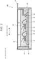
- FIG. 2 is a schematic cross-sectional view of the semiconductor device of the embodiment.
- FIG. 2 represents the cross section along AA' of FIG. 1 .
- FIG. 3 is an equivalent circuit diagram of the semiconductor device of the embodiment.
- the semiconductor device of the embodiment is a power semiconductor module 100.
- the power semiconductor module 100 of the embodiment is a so-called "2 in 1" type module in which a half bridge circuit may be configured with one module.
- a half bridge circuit may be configured with one module.
- three half bridge units are connected in parallel.
- a three-phase inverter circuit may be implemented by three power semiconductor modules of the embodiment.
- the power semiconductor module 100 includes a positive terminal P (a first main terminal), a negative terminal N (a second main terminal), an AC output terminal AC (an output terminal), and multiple high-side MOSFETs 11 (first semiconductor chips) and multiple low-side MOSFETs 21 (second semiconductor chips).
- Each MOSFET is equipped with a Schottky barrier diode (SBD), in addition to a pn junction diode.
- SBD has, for example, a function of causing the flow of a reflux current.
- the multiple high-side MOSFETs 11 are connected in parallel.
- the multiple low-side MOSFETs 21 are connected in parallel.
- the multiple high-side MOSFETs 11 and the multiple low-side MOSFETs 21 are connected in series.
- FIGS. 1 to 3 illustrate a case where the number of high-side MOSFETs 11 is three, and the number of low-side MOSFETs 21 is three.
- the power semiconductor module 100 of the embodiment is provided with the positive terminal P (the first main terminal), the negative terminal N (the second main terminal), the AC output terminal AC (the output terminal), the multiple high-side MOSFETs 11 (the first semiconductor chips), the multiple low-side MOSFETs 21 (the second semiconductor chips), a resin housing 24, a lid 26, a metal base 28, an insulating substrate 30, a first metal layer 31, and a second metal layer 32, a third metal layer 33, a first gate metal layer 36 (a fourth metal layer), a second gate metal layer 37 (a fifth metal layer), a back-surface metal layer 40, a first gate terminal 41, a second gate terminal 42, first bonding wires 44 (first connection wires), second bonding wires 46 (second connection wires), gate bonding wires 48, and a sealing resin 50.
- Each of the multiple high-side MOSFETs 11 includes a first source electrode 11a (a first upper electrode), a first drain electrode 11b (a first lower electrode), and a first gate electrode 11c, a first silicon carbide layer 11x, and a first Schottky barrier diode 11y.
- Each of the multiple low-side MOSFETs 21 includes a second source electrode 21a (a second upper electrode), a second drain electrode 21b (a second lower electrode), a second gate electrode 21c, a second silicon carbide layer 21x, and a second Schottky barrier diode 21y.
- the first metal layer 31 has a first connection region 31x.
- the second metal layer 32 has a second connection region 32x.
- the third metal layer 33 has a third connection region 33x.
- FIG. 1 is a top view of the power semiconductor module 100 in a state where the lid 26 and the sealing resin 50 are removed.
- the metal base 28 is, for example, copper.
- a heat dissipation plate (not illustrated) is connected to the back surface of the metal base 28.
- the insulating substrate 30 is provided on the metal base 28.
- the insulating substrate 30 is provided between the metal base 28 and the high-side MOSFETs 11, and between the metal base 28 and the low-side MOSFETs 21.
- the insulating substrate 30 has a function of electrically separating the metal base 28 and the high-side MOSFETs 11, and the metal base 28 and the low-side MOSFETs 21.
- the insulating substrate 30 is, for example, ceramic.
- the insulating substrate 30 is, for example, aluminum oxide, aluminum nitride, or silicon nitride.
- the first metal layer 31, the second metal layer 32, the third metal layer 33, the first gate metal layer 36, and the second gate metal layer 37 are formed on the surface of the insulating substrate 30.
- the first metal layer 31, the second metal layer 32, the third metal layer 33, the first gate metal layer 36, and the second gate metal layer 37 are, for example, copper.
- the back-surface metal layer 40 is formed on the back surface of the insulating substrate 30.
- the back-surface metal layer 40 is, for example, copper.
- the back-surface metal layer 40 is joined to the metal base 28 by using, for example, a solder layer or a silver nanoparticle layer (not illustrated).
- the resin housing 24 is provided around the metal base 28 and the insulating substrate 30. A portion of the resin housing 24 is provided on the metal base 28.
- the resin housing 24 has a function of protecting the high-side MOSFETs 11, the low-side MOSFETs 21, and the insulating substrate 30.
- the lid 26 is provided on the resin housing 24.
- the lid 26 has a function of protecting the high-side MOSFETs 11, the low-side MOSFETs 21, and the insulating substrate 30.
- the multiple high-side MOSFETs 11 are provided on the first metal layer 31.
- Each of the multiple high-side MOSFETs 11 includes the first source electrode 11a, the first drain electrode 11b, the first gate electrode 11c, the first silicon carbide layer 11x, and the first Schottky barrier diode 11y.
- the first source electrode 11a is an example of the first upper electrode.
- the first drain electrode 11b is an example of the first lower electrode.
- the first source electrode 11a is electrically connected to the third metal layer 33.
- the first source electrode 11a and the third metal layer 33 are electrically connected to each other, by using, for example, a first bonding wire 44.
- the first drain electrode 11b is electrically connected to the first metal layer 31.
- the first drain electrode 11b is electrically connected to the first metal layer 31 by using, for example, a solder layer or a silver nanoparticle layer (not illustrated).
- the multiple high-side MOSFETs 11 are arranged in a first direction parallel to the insulating substrate 30.
- the multiple low-side MOSFETs 21 are provided on the third metal layer 33.
- Each of the multiple low-side MOSFETs 21 includes the second source electrode 21a, the second drain electrode 21b, the second gate electrode 21c, the second silicon carbide layer 21x, and the second Schottky barrier diode 21y.
- the second source electrode 21a is an example of the second upper electrode.
- the second drain electrode 21b is an example of the second lower electrode.
- the second source electrode 21a is electrically connected to the second metal layer 32.
- the second source electrode 21a and the second metal layer 32 are electrically connected to each other, by using, for example, a second bonding wire 46.
- the second drain electrode 21b is electrically connected to the third metal layer 33.
- the second drain electrode 21b is electrically connected to the third metal layer 33 by using, for example, a solder layer or a silver nanoparticle layer (not illustrated).
- the multiple low-side MOSFETs 21 are arranged in the first direction parallel to the insulating substrate 30.
- the sealing resin 50 is filled in the resin housing 24.
- the sealing resin 50 is surrounded by the resin housing 24.
- the sealing resin 50 covers the high-side MOSFETs 11, the low-side MOSFETs 21, and the insulating substrate 30.
- the sealing resin 50 has a function of protecting the high-side MOSFETs 11, the low-side MOSFETs 21, and the insulating substrate 30. Further, the sealing resin 50 has a function of insulating the high-side MOSFETs 11, the low-side MOSFETs 21, and the insulating substrate 30 from each other.
- the sealing resin 50 contains a resin.
- the sealing resin 50 is, for example, a silicon gel.
- an epoxy resin, a polyimide resin or other resins may be applied.
- the positive terminal P is provided on one end side of the insulating substrate 30.
- the positive terminal P is provided on the right side of the insulating substrate 30.
- the positive terminal P has a wiring connection hole.
- the positive terminal P is electrically connected to the first metal layer 31 in the first connection region 31x.
- the first metal layer 31 and the positive terminal P are connected to each other by using, for example, a solder layer or a silver nanoparticle layer (not illustrated).
- a positive voltage is applied to the positive terminal P from the outside.
- the positive terminal P is made of a metal.
- the positive terminal P is, for example, copper.
- the negative terminal N is provided on one end side of the insulating substrate 30.
- the negative terminal N is provided on the same side of the insulating substrate 30 as the side thereof on which the positive terminal P is provided.
- the negative terminal N has a wiring connection hole.
- the negative terminal N is electrically connected to the second metal layer 32 in the second connection region 32x.
- the second metal layer 32 and the negative terminal N are connected to each other by using, for example, a solder layer or a silver nanoparticle layer (not illustrated).
- a negative voltage is applied to the negative terminal N from the outside.
- the negative terminal N is made of a metal.
- the negative terminal N is, for example, copper.
- the AC output terminal AC is provided on one end side of the insulating substrate 30.
- the AC output terminal AC is provided on the same side of the insulating substrate 30 as the side thereof on which the positive terminal P and the negative terminal N are provided.
- the AC output terminal AC has a wiring connection hole.
- the AC output terminal AC is electrically connected to the third metal layer 33 in the third connection region 33x.
- the third metal layer 33 and the AC output terminal AC are connected to each other by using, for example, a solder layer or a silver nanoparticle layer (not illustrated).
- the AC output terminal AC outputs output currents of the half bridge circuits.
- the AC output terminal AC is made of a metal.
- the AC output terminal AC is, for example, copper.
- the first gate terminal 41 is electrically connected to the first gate electrodes 11c of the high-side MOSFETs 11.
- the first gate terminal 41 is electrically connected to the first gate electrodes 11c by using, for example, the first gate metal layer 36 and a gate bonding wire 48.
- the second gate terminal 42 is electrically connected to the second gate electrodes 21c of the low-side MOSFETs 21.
- the second gate terminal 42 is electrically connected to the second gate electrodes 21c by using, for example, the second gate metal layer 37 and a gate bonding wire 48.
- the first metal layer 31 is formed on the insulating substrate 30.
- the first metal layer 31 has the first connection region 31x.
- the first metal layer 31 is electrically connected to the positive terminal P in the first connection region 31x.
- the second metal layer 32 is formed on the insulating substrate 30.
- the second metal layer 32 has the second connection region 32x.
- the second metal layer 32 is electrically connected to the negative terminal N in the second connection region 32x.
- the second metal layer 32 is electrically connected to the second source electrodes 21a of the low-side MOSFETs 21.
- the third metal layer 33 is formed on the insulating substrate 30.
- the third metal layer 33 includes the third connection region 33x.
- the third metal layer 33 is electrically connected to the AC output terminal AC in the third connection region 33x.
- the third metal layer 33 is electrically connected to the first source electrodes 11a of the high-side MOSFETs 11.
- a respective one of the multiple low-side MOSFETs 21 exists in a second direction perpendicular to the first direction and parallel to the insulating substrate 30, for each of the multiple high-side MOSFETs 11.
- each high-side MOSFET 11 is provided adjacent to each low-side MOSFET 21 in the second direction.
- the direction that connects the first connection region 31x and the second connection region 32x to each other is defined as a third direction.
- the third direction is the direction of the segment that connects the first connection region 31x and the second connection region 32x with the shortest distance.
- the angle formed by the third direction and the first direction is 20° or less.
- the third direction is parallel to the first direction.
- the angle formed by the third direction and the first direction is 0°.
- the multiple high-side MOSFETs 11 are arranged in the third direction.
- the multiple low-side MOSFETs 21 are arranged in the third direction.
- the angle formed by the extension direction of the first bonding wire 44 and the second direction is 20° or less.
- the angle formed by the extension direction of at least one of the multiple first bonding wires 44 and the second direction is 20° or less.
- the angle formed by the extension direction of the first bonding wire 44 connected to any one of the multiple high-side MOSFETs 11 and the second direction is 20° or less.
- the angle formed by the extension direction of the first bonding wire 44 and the third direction is 70° or more and 90° or less.
- the angle formed by the extension direction of at least one of the multiple first bonding wires 44 and the third direction is 70° or more and 90° or less.
- the angle formed by the extension direction of the first bonding wire 44 connected to any one of the multiple high-side MOSFETs 11 and the third direction is 70° or more and 90° or less.
- extension direction of the first bonding wire 44 is, for example, the direction of the segment that connects the position where the first bonding wire 44 is in contact with the first source electrode 11a and the position where the first bonding wire 44 is in contact with the third metal layer 33.
- the angle formed by the extension directions of all of the first bonding wires 44 provided in the semiconductor module 100 and the second direction is 20° or less.
- FIG. 1 represents a case where the angle formed by the extension directions of all of the first bonding wires 44 provided in the semiconductor module 100 and the second direction is 0°.
- the angle formed by the extension direction of the second bonding wire 46 and the second direction is 20° or less.
- the angle formed by the extension direction of at least one of the multiple second bonding wires 46 and the second direction is 20° or less.
- the angle formed by the extension direction of the second bonding wire 46 connected to any one of the multiple low-side MOSFETs 21 and the second direction is 20° or less.
- the angle formed by the extension direction of the second bonding wire 46 connected to the second source electrode 21a of the low-side MOSFET 21 closest to the first metal layer 31 in the first direction, among the multiple low-side MISFETs 21, and the second direction is 20° or less. That is, in FIG. 1 , the angle formed by the extension direction of the second bonding wire 46 connected to the second source electrode 21a of the low-side MOSFET 21 at the lowest side, among the multiple low-side MOSFETs 21, and the second direction is 20° or less.
- the angle formed by the extension direction of the second bonding wire 46 and the third direction is 70° or more and 90° or less.
- the angle formed by the extension direction of at least one of the multiple second bonding wires 46 and the third extension direction is 70° or more and 90° or less.
- the angle formed by the extension direction of the second bonding wire 46 connected to any one of the multiple low-side MOSFETs 21 and the third direction is 70° or more and 90° or less.
- extension direction of the second bonding wire 46 is, for example, the direction of the segment that connects the position where the second bonding wire 46 is in contact with the second source electrode 21a and the position where the second bonding wire 46 is in contact with the second metal layer 32.
- the angle formed by the extension directions of all of the second bonding wires 46 provided in the semiconductor module 100 and the second direction is 20° or less.
- FIG. 1 represents a case where the extension directions of all of the second bonding wires 46 provided in the semiconductor module 100 and the second direction is 0°.
- the second metal layer 32 exists in the second direction of the low-side MOSFET 21 closest to the first metal layer 31 in the first direction, among the multiple low-side MOSFETs 21. That is, in FIG. 1 , the second metal layer 32 exists in the second direction of the low-side MOSFET 21 at the lowest side, among the multiple low-side MOSFETs 21.
- the second metal layer 32 exists in the second direction of the contact points between the second source electrode 21a of the low-side MOSFET 21 closest to the first metal layer 31 in the first direction (C1 and C2 in FIG. 1 ), among the multiple low-side MOSFETs 21, and the second bonding wires 46.
- the second metal layer 32 exists in the second direction of the contact point closest to the first metal layer 31 (C2 in FIG. 1 ).
- the second metal layer 32 exists in the second direction of the end of the low-side MOSFET 21 closest to the first metal layer 31 in the first direction, the end which is close to the first metal layer 31 (E1 in FIG. 1 ).
- a first distance in the first direction between the second connection region 32x and the end of the second metal layer 32 close to the first metal layer 31 is larger than a second distance in the first direction between the end of the low-side MOSFET 21 closest to the first metal layer 31 in the first direction among the multiple low-side MOSFETs 21, the end which is away from the first metal layer 31, and the end of the second metal layer 32 close to the first metal layer 31 (d2 in FIG. 1 ).
- the first distance in the first direction between the second connection region 32x and the end of the second metal layer 32 close to the first metal layer 31 is larger than a third distance in the first direction between the second connection region 32x and the end of the second metal layer 32 which is opposite to the first metal layer 31 (d3 in FIG. 1 ).
- a vertical MOSFET using silicon carbide has the pn junction diode as a body diode.
- the MOSFET is used as a switching element connected to an inductive load. In this case, even when the MOSFET is OFF, a reflux current may be caused to flow by using the body diode.
- FIG. 4 is a schematic top view of a semiconductor device of a comparative example.
- the semiconductor device of the comparative example is a power semiconductor module 900.
- the equivalent circuit diagram of the power semiconductor module 900 is the same as illustrated in FIG.3 .
- the power semiconductor module 900 is different from the power semiconductor module 100 of the embodiment in that the first direction in which the multiple high-side MOSFETs 11 are arranged is perpendicular to the third direction. Further, the power semiconductor module 900 is different from the power semiconductor module 100 of the embodiment in that the first direction in which the multiple low-side MOSFETs 21 are arranged is perpendicular to the third direction.
- the third direction is the direction that connects the first connection region 31x and the second connection region 32x.
- the power semiconductor module 900 is different from the power semiconductor module 100 of the embodiment in that the angle formed by the extension direction of the first bonding wire 44 and the third direction is parallel. Further, as illustrated in FIG. 4 , the power semiconductor module 900 is different from the power semiconductor module 100 of the embodiment in that the angle formed by the extension direction of the second bonding wire 46 and the third direction is parallel.
- FIG. 5 is a view illustrating the problem of the semiconductor device of the comparative example.
- FIG. 5 is a schematic top view of the power semiconductor module 900.
- FIG. 5 represents three routes from the positive terminal P to the negative terminal N through the MOSFETs, that is, routes X9, Y9, and Z9 by dashed arrows.
- the routes X9, Y9, and Z9 are routes from the first connection region 31x to the second connection region 32x.
- the route X9 is the shortest route
- the route Z9 is the longest route.
- the current flowing through the diodes of the MOSFETs existing in the route X9, which is the shortest route, is the largest.
- the current flowing through the diodes of the MOSFETs existing in the route Z9, which is the longest route, is the smallest.
- the power semiconductor module 900 is connected to an external inductive load, the multiple high-side MOSFETs 11 are in an OFF state, and the multiple low-side MOSFETs 21 are in an ON state in which the current flows. From this state, the multiple high-side MOSFETs 11 are switched to the ON state, and the multiple low-side MOSFETs 21 are switched to the OFF state. At this time, the multiple low-side MOSFETs 21 enter a reverse conduction state, and a reflux current flows through the diodes equipped in the low-side MOSFETs 21.
- the pn junction diode When the reflux current flowing through the diodes of the low-side MOSFETs 21 existing in the route X9 exceeds an allowable current range of a second Schottky barrier diode 21y provided in the low-side MOSFET 21, the pn junction diode operates. When the pn junction diode operates, the reliability of the low-side MOSFETs 21 existing in the route X9 is degraded. Then, the reliability of the power semiconductor module 900 is degraded.
- FIG. 6 is a view illustrating the operation and effects of the semiconductor device of the embodiment.
- FIG. 6 is a schematic top view of the power semiconductor module 100.
- FIG. 6 represents three routes from the positive terminal P to the negative terminal N through the MOSFETs, that is, routes X1, Y1, and Z1 by dashed arrows.
- the routes X1, Y1, and Z1 are routes from the first connection region 31x to the second connection region 32x.
- the power semiconductor module 100 of the first embodiment reduces the variation of the lengths of the routes X1, Y1, and Z1 by changing the arrangement direction of the MOSFETs and the extension direction of the bonding wires, as compared with the power semiconductor module 900 of the comparative example.
- the multiple high-side MOSFETs 11 are arranged along the third direction that connects the first connection region 31x and the second connection region 32x.
- the multiple low-side MOSFETs 21 are also arranged along the third direction.
- the angle formed by the third direction and the first direction in which the multiple high-side MOSFETs 11 and the multiple low-side MOSFETs 21 are arranged is 20° or less.
- the angle formed by the extension direction of the first bonding wire 44 and the second direction is 20° or less.
- the angle formed by the extension direction of the second bonding wire 46 and the second direction is 20° or less.
- the power semiconductor module 100 of the embodiment reduces the variation of the lengths of the routes X1, Y1, and Z1.
- the variation of the currents flowing through the diodes during the switching operation of the power semiconductor module 100 is reduced. Accordingly, the operation of the pn junction diode provided in each MOSFET is prevented. As a result, the reliability of the power semiconductor module 100 is improved.
- the angle formed by the third direction and the first direction in which the multiple high-side MOSFETs 11 and the multiple low-side MOSFETs 21 are arranged is preferably 10° or less, more preferably 5° or less, and most preferably 0°. As the angle becomes smaller, the variation of the lengths of the routes X1, Y1, and Z1 is further reduced.
- the angle formed by the extension directions of all of the first bonding wires 44 provided in the semiconductor module 100 and the second direction is preferably 20° or less. Further, the angle formed by the extension directions of all of the second bonding wires 46 provided in the semiconductor module 100 and the second direction is preferably 20° or less. With this configuration, the variation of the lengths of the routes X1, Y1, and Z1 is further reduced.
- the angle formed by the extension direction of the first bonding wire 44 and the second direction is preferably 10° or less, more preferably 5° or less, and most preferably 0°.
- the angle formed by the extension direction of the second bonding wire 46 and the second direction is preferably 10° or less, more preferably 5° or less, and most preferably 0°. As the angle becomes smaller, the variation of the lengths of the routes X1, Y1, and Z1 is further reduced.
- the second metal layer 32 exists in the second direction of the low-side MOSFET 21 closest to the first metal layer 31 in the first direction, among the multiple low-side MOSFETs 21. That is, in FIG. 1 , it is preferable that the second metal layer 32 exists in the second direction of the low-side MOSFET 21 at the lowest side among the multiple low-side MOSFETs 21. With this configuration, the variation of the lengths of the routes X1, Y1, and Z1 is further reduced.
- the second metal layer 32 exists in the second direction of the contact points between the second source electrode 21a of the low-side MOSFET 21 closest to the first metal layer 31 in the first direction (C1 and C2 in FIG. 1 ), among the multiple low-side MOSFETs 21, and the second bonding wires 46. It is preferable that, of the contact points between the second source electrode 21a of the low-side MOSFET 21 closest to the first metal layer 31 in the first direction among the multiple low-side MOSFETs 21, and the second bonding wires 46, the second metal layer 32 exists in the second direction of the contact point closest to the first metal layer 31 (C2 in FIG. 1 ). With this configuration, the variation of the lengths of the routes X1, Y1, and Z1 is further reduced.
- the second metal layer 32 exists in the second direction of the end of the low-side MOSFET 21 closest to the first metal layer 31 in the first direction among the multiple low-side MOSFETs 21, the end which is close to the first metal layer 31 (E1 in FIG. 1 ). With this configuration, the variation of the lengths of the routes X1, Y1, and Z1 is further reduced.
- the first distance in the first direction between the second connection region 32x and the end of the second metal layer 32 close to the first metal layer 31 (d1 in FIG. 1 ) is larger than the second distance in the first direction between the end of the low-side MOSFET 21 closest to the first metal layer 31 in the first direction among the multiple low-side MOSFETs 21, the end which is away from the first metal layer 31, and the end of the second metal layer 32 close to the first metal layer 31 (d2 in FIG. 1 ).
- the first distance in the first direction between the second connection region 32x and the end of the second metal layer 32 close to the first metal layer 31 (d1 in FIG. 1 ) is larger than the third distance in the first direction between the second connection region 32x and the end of the second metal layer 32 which is opposite to the first metal layer 31 (d3 in FIG. 1 ).
- the number of power semiconductor chips arranged in parallel is three, as an example.
- the number of power semiconductor chips may be two or four or more.
- the power semiconductor module is a "2 in 1" type module, as an example.
- the power semiconductor module may have other circuit configurations such as, for example, a "4 in 1" type module and a "6 in 1" type module.
- the first and second bonding wires may be linear bonding wires or ribbon-shaped bonding wires. Further, the first and second bonding wires may be, for example, plate-shaped conductors if the conductors have the function of performing an electric connection.
- the terminal such as the positive terminal P or the like is directly connected to the metal layer, as an example.
- the terminal and the metal layer may be connected by, for example, a bonding wire.
- the positive terminal, the negative terminal, and the AC output terminal are all provided at the same end of the power semiconductor module, as an example.
- the arrangement positions of the positive terminal, the negative terminal, and the AC output terminal are not limited to the arrangement positions described above.
Landscapes
- Engineering & Computer Science (AREA)
- Power Engineering (AREA)
- Microelectronics & Electronic Packaging (AREA)
- Electrodes Of Semiconductors (AREA)
- Electronic Switches (AREA)
- Semiconductor Integrated Circuits (AREA)
Abstract
According to one embodiment, a semiconductor device includes: a first metal layer connected to a first main terminal in a first connection region; a second metal layer connected to a second main terminal in a second connection region; a third metal layer connected to an output terminal; a plurality of first semiconductor chips each including a first upper electrode, a first lower electrode, a first gate electrode, and a first Schottky barrier diode, and arranged in a first direction in a state where the first lower electrode is connected to the first metal layer; a plurality of second semiconductor chips each including a second upper electrode, a second lower electrode, a second gate electrode, and a second Schottky barrier diode, and arranged in the first direction in a state where the second lower electrode is connected to the third metal layer; a first connection wire configured to connect the first upper electrode and the third metal layer; and a second connection wire configured to connect the second upper electrode and the second metal layer. The angle formed by the third direction that connects the first and second connection regions, and the first direction is 20° or less. The angle formed by the extension directions of the first and second connection wires and a second direction perpendicular to the first direction is 20° or less.
Description
- This application is based upon and claims the benefit of priority from
Japanese Patent Application No. 2021-152688, filed September 17, 2021 - Embodiments described herein relate generally to a semiconductor device.
- Silicon carbide is expected as a material for next-generation semiconductor devices. Silicon carbide has excellent physical properties such as an about 3 times larger bandgap, an about 10 times stronger breakdown electric field strength, and an about 3 times higher thermal conductivity, as compared to silicon. By utilizing these properties, for example, a metal oxide semiconductor field effect transistor (MOSFET) which is operable at a high temperature with a high pressure resistance and a low loss may be implemented.
- A vertical MOSFET using silicon carbide has a pn junction diode as a body diode. For example, the MOSFET is used as a switching element connected to an inductive load. In this case, even when the MOSFET is OFF, a reflux current may be caused to flow by using the body diode.
- However, when the reflux current is caused to flow by using the body diode, a problem occurs in that a stacking defect grows in the silicon carbide layer due to recombination energy of carriers, and thus, the ON-resistance of the MOSFET increases. The increase in ON-resistance of the MOSFET causes a degradation of the reliability of the MOSFET.
- There is a MOSFET equipped with a Schottky barrier diode (SBD) that operates in a unipolar manner. When the reflux current is caused to flow by using the SBD instead of the pn junction diode that operates in a bipolar manner, the growth of stacking defect is prevented. Thus, the reliability of the MOSFET is improved.
-
-
FIG. 1 is a schematic top view illustrating a semiconductor device according to an embodiment. -
FIG. 2 is a schematic cross-sectional view of the semiconductor device according to the embodiment. -
FIG. 3 is an equivalent circuit diagram of the semiconductor device of the embodiment. -
FIG. 4 is a schematic top view of a semiconductor device of a comparative example. -
FIG. 5 is a view illustrating a problem of the semiconductor device of the comparative example. -
FIG. 6 is a view illustrating an operation and effects of the semiconductor device according to the embodiment. - In general, according to one embodiment, a semiconductor device includes: an insulating substrate; a first main terminal; a second main terminal; an output terminal; a first metal layer formed on the insulating substrate, provided with a first connection region, and electrically connected to the first main terminal in the first connection region; a second metal layer formed on the insulating substrate, provided with a second connection region, and electrically connected to the second main terminal in the second connection region; a third metal layer formed on the insulating substrate to be disposed between the first metal layer and the second metal layer, provided with a third connection region, and electrically connected to the output terminal in the third connection region; a plurality of first semiconductor chips each including a first upper electrode, a first lower electrode, a first gate electrode, a first silicon carbide layer, and a first Schottky barrier diode, and arranged in a first direction in a state where the first lower electrode is electrically connected to the first metal layer; a plurality of second semiconductor chips each including a second upper electrode, a second lower electrode, a second gate electrode, a second silicon carbide layer, and a second Schottky barrier diode, and arranged in the first direction in a state where the second lower electrode is electrically connected to the third metal layer; a first connection wire configured to electrically connect the first upper electrode and the third metal layer; and a second connection wire configured to electrically connect the second upper electrode and the second metal layer. The second semiconductor chips exist in a second direction perpendicular to the first direction of the first semiconductor chips and parallel to the insulating substrate. An angle formed by the third direction that connects the first connection region and the second connection region, and the first direction is 20° or less. An angle formed by an extension direction of the first connection wire and the second direction is 20° or less. An angle formed by an extension direction of the second connection wire connected to the second upper electrode of a second semiconductor chip closest to the first metal layer in the first direction among the plurality of second semiconductor chips, and the second direction is 20° or less.
- In the descriptions herein, the same or similar members may be denoted by the same reference numerals, and overlapping descriptions thereof may be omitted.
- In the descriptions herein, in order to indicate the positional relationship of components and others, the upward direction of each drawing may be described as "upper (above)", and the downward direction of each drawing may be described as "lower (below)". In the descriptions herein, the concepts of "upper" and "lower" do not necessarily indicate the relationship with the direction of gravity.
- A semiconductor device of an embodiment includes: an insulating substrate; a first main terminal; a second main terminal; an output terminal; a first metal layer formed on the insulating substrate, provided with a first connection region, and electrically connected to the first main terminal in the first connection region; a second metal layer formed on the insulating substrate, provided with a second connection region, and electrically connected to the second main terminal in the second connection region; a third metal layer formed on the insulating substrate to be disposed between the first metal layer and the second metal layer, provided with a third connection region, and electrically connected to the output terminal in the third connection region; a plurality of first semiconductor chips each including a first upper electrode, a first lower electrode, a first gate electrode, a first silicon carbide layer, and a first Schottky barrier diode, and arranged in a first direction in a state where the first lower electrode is electrically connected to the first metal layer; a plurality of second semiconductor chips each including a second upper electrode, a second lower electrode, a second gate electrode, a second silicon carbide layer, and a second Schottky barrier diode, and arranged in the first direction in a state where the second lower electrode is electrically connected to the third metal layer; a first connection wire configured to electrically connect the first upper electrode and the third metal layer; and a second connection wire configured to electrically connect the second upper electrode and the second metal layer. The second semiconductor chips exist in a second direction perpendicular to the first direction of the first semiconductor chips and parallel to the insulating substrate. An angle formed by the third direction that connects the first connection region and the second connection region, and the first direction is 20° or less, and an angle formed by an extension direction of the first connection wire and the second direction is 20° or less. An angle formed by an extension direction of the second connection wire connected to the second upper electrode of a second semiconductor chip closest to the first metal layer in the first direction among the plurality of second semiconductor chips, and the second direction is 20° or less.
-
FIG. 1 is a schematic top view of a semiconductor device of an embodiment.FIG. 2 is a schematic cross-sectional view of the semiconductor device of the embodiment.FIG. 2 represents the cross section along AA' ofFIG. 1 .FIG. 3 is an equivalent circuit diagram of the semiconductor device of the embodiment. - The semiconductor device of the embodiment is a
power semiconductor module 100. As illustrated inFIG. 3 , thepower semiconductor module 100 of the embodiment is a so-called "2 in 1" type module in which a half bridge circuit may be configured with one module. In thepower semiconductor module 100, three half bridge units are connected in parallel. For example, a three-phase inverter circuit may be implemented by three power semiconductor modules of the embodiment. - As illustrated in
FIG. 3 , thepower semiconductor module 100 includes a positive terminal P (a first main terminal), a negative terminal N (a second main terminal), an AC output terminal AC (an output terminal), and multiple high-side MOSFETs 11 (first semiconductor chips) and multiple low-side MOSFETs 21 (second semiconductor chips). Each MOSFET is equipped with a Schottky barrier diode (SBD), in addition to a pn junction diode. The SBD has, for example, a function of causing the flow of a reflux current. - The multiple high-
side MOSFETs 11 are connected in parallel. The multiple low-side MOSFETs 21 are connected in parallel. The multiple high-side MOSFETs 11 and the multiple low-side MOSFETs 21 are connected in series. -
FIGS. 1 to 3 illustrate a case where the number of high-side MOSFETs 11 is three, and the number of low-side MOSFETs 21 is three. - As illustrated in
FIGS. 1 and2 , thepower semiconductor module 100 of the embodiment is provided with the positive terminal P (the first main terminal), the negative terminal N (the second main terminal), the AC output terminal AC (the output terminal), the multiple high-side MOSFETs 11 (the first semiconductor chips), the multiple low-side MOSFETs 21 (the second semiconductor chips), aresin housing 24, alid 26, ametal base 28, aninsulating substrate 30, afirst metal layer 31, and asecond metal layer 32, athird metal layer 33, a first gate metal layer 36 (a fourth metal layer), a second gate metal layer 37 (a fifth metal layer), a back-surface metal layer 40, afirst gate terminal 41, asecond gate terminal 42, first bonding wires 44 (first connection wires), second bonding wires 46 (second connection wires),gate bonding wires 48, and asealing resin 50. - Each of the multiple high-side MOSFETs 11 (the first semiconductor chips) includes a
first source electrode 11a (a first upper electrode), afirst drain electrode 11b (a first lower electrode), and a first gate electrode 11c, a firstsilicon carbide layer 11x, and a first Schottky barrier diode 11y. - Each of the multiple low-side MOSFETs 21 (the second semiconductor chips) includes a
second source electrode 21a (a second upper electrode), a second drain electrode 21b (a second lower electrode), a second gate electrode 21c, a second silicon carbide layer 21x, and a second Schottky barrier diode 21y. - The
first metal layer 31 has afirst connection region 31x. Thesecond metal layer 32 has asecond connection region 32x. Thethird metal layer 33 has athird connection region 33x. -
FIG. 1 is a top view of thepower semiconductor module 100 in a state where thelid 26 and thesealing resin 50 are removed. - The
metal base 28 is, for example, copper. For example, when thepower semiconductor module 100 is mounted on a product, a heat dissipation plate (not illustrated) is connected to the back surface of themetal base 28. - The
insulating substrate 30 is provided on themetal base 28. Theinsulating substrate 30 is provided between themetal base 28 and the high-side MOSFETs 11, and between themetal base 28 and the low-side MOSFETs 21. - The
insulating substrate 30 has a function of electrically separating themetal base 28 and the high-side MOSFETs 11, and themetal base 28 and the low-side MOSFETs 21. - The
insulating substrate 30 is, for example, ceramic. Theinsulating substrate 30 is, for example, aluminum oxide, aluminum nitride, or silicon nitride. - The
first metal layer 31, thesecond metal layer 32, thethird metal layer 33, the firstgate metal layer 36, and the secondgate metal layer 37 are formed on the surface of the insulatingsubstrate 30. Thefirst metal layer 31, thesecond metal layer 32, thethird metal layer 33, the firstgate metal layer 36, and the secondgate metal layer 37 are, for example, copper. - The back-
surface metal layer 40 is formed on the back surface of the insulatingsubstrate 30. The back-surface metal layer 40 is, for example, copper. The back-surface metal layer 40 is joined to themetal base 28 by using, for example, a solder layer or a silver nanoparticle layer (not illustrated). - The
resin housing 24 is provided around themetal base 28 and the insulatingsubstrate 30. A portion of theresin housing 24 is provided on themetal base 28. Theresin housing 24 has a function of protecting the high-side MOSFETs 11, the low-side MOSFETs 21, and the insulatingsubstrate 30. - The
lid 26 is provided on theresin housing 24. Thelid 26 has a function of protecting the high-side MOSFETs 11, the low-side MOSFETs 21, and the insulatingsubstrate 30. - The multiple high-
side MOSFETs 11 are provided on thefirst metal layer 31. Each of the multiple high-side MOSFETs 11 includes thefirst source electrode 11a, thefirst drain electrode 11b, the first gate electrode 11c, the firstsilicon carbide layer 11x, and the first Schottky barrier diode 11y. Thefirst source electrode 11a is an example of the first upper electrode. Thefirst drain electrode 11b is an example of the first lower electrode. - The
first source electrode 11a is electrically connected to thethird metal layer 33. Thefirst source electrode 11a and thethird metal layer 33 are electrically connected to each other, by using, for example, afirst bonding wire 44. Thefirst drain electrode 11b is electrically connected to thefirst metal layer 31. Thefirst drain electrode 11b is electrically connected to thefirst metal layer 31 by using, for example, a solder layer or a silver nanoparticle layer (not illustrated). - The multiple high-
side MOSFETs 11 are arranged in a first direction parallel to the insulatingsubstrate 30. - The multiple low-
side MOSFETs 21 are provided on thethird metal layer 33. Each of the multiple low-side MOSFETs 21 includes thesecond source electrode 21a, the second drain electrode 21b, the second gate electrode 21c, the second silicon carbide layer 21x, and the second Schottky barrier diode 21y. Thesecond source electrode 21a is an example of the second upper electrode. The second drain electrode 21b is an example of the second lower electrode. - The
second source electrode 21a is electrically connected to thesecond metal layer 32. Thesecond source electrode 21a and thesecond metal layer 32 are electrically connected to each other, by using, for example, asecond bonding wire 46. The second drain electrode 21b is electrically connected to thethird metal layer 33. The second drain electrode 21b is electrically connected to thethird metal layer 33 by using, for example, a solder layer or a silver nanoparticle layer (not illustrated). - The multiple low-
side MOSFETs 21 are arranged in the first direction parallel to the insulatingsubstrate 30. - The sealing
resin 50 is filled in theresin housing 24. The sealingresin 50 is surrounded by theresin housing 24. The sealingresin 50 covers the high-side MOSFETs 11, the low-side MOSFETs 21, and the insulatingsubstrate 30. - The sealing
resin 50 has a function of protecting the high-side MOSFETs 11, the low-side MOSFETs 21, and the insulatingsubstrate 30. Further, the sealingresin 50 has a function of insulating the high-side MOSFETs 11, the low-side MOSFETs 21, and the insulatingsubstrate 30 from each other. - The sealing
resin 50 contains a resin. The sealingresin 50 is, for example, a silicon gel. For the sealingresin 50, for example, an epoxy resin, a polyimide resin or other resins may be applied. - The positive terminal P is provided on one end side of the insulating
substrate 30. For example, inFIG. 1 , the positive terminal P is provided on the right side of the insulatingsubstrate 30. The positive terminal P has a wiring connection hole. - The positive terminal P is electrically connected to the
first metal layer 31 in thefirst connection region 31x. In thefirst connection region 31x, thefirst metal layer 31 and the positive terminal P are connected to each other by using, for example, a solder layer or a silver nanoparticle layer (not illustrated). - For example, a positive voltage is applied to the positive terminal P from the outside. The positive terminal P is made of a metal. The positive terminal P is, for example, copper.
- The negative terminal N is provided on one end side of the insulating
substrate 30. The negative terminal N is provided on the same side of the insulatingsubstrate 30 as the side thereof on which the positive terminal P is provided. The negative terminal N has a wiring connection hole. - The negative terminal N is electrically connected to the
second metal layer 32 in thesecond connection region 32x. In thesecond connection region 32x, thesecond metal layer 32 and the negative terminal N are connected to each other by using, for example, a solder layer or a silver nanoparticle layer (not illustrated). - For example, a negative voltage is applied to the negative terminal N from the outside. The negative terminal N is made of a metal. The negative terminal N is, for example, copper.
- The AC output terminal AC is provided on one end side of the insulating
substrate 30. The AC output terminal AC is provided on the same side of the insulatingsubstrate 30 as the side thereof on which the positive terminal P and the negative terminal N are provided. The AC output terminal AC has a wiring connection hole. - The AC output terminal AC is electrically connected to the
third metal layer 33 in thethird connection region 33x. In thethird connection region 33x, thethird metal layer 33 and the AC output terminal AC are connected to each other by using, for example, a solder layer or a silver nanoparticle layer (not illustrated). - The AC output terminal AC outputs output currents of the half bridge circuits. The AC output terminal AC is made of a metal. The AC output terminal AC is, for example, copper.
- The
first gate terminal 41 is electrically connected to the first gate electrodes 11c of the high-side MOSFETs 11. Thefirst gate terminal 41 is electrically connected to the first gate electrodes 11c by using, for example, the firstgate metal layer 36 and agate bonding wire 48. - The
second gate terminal 42 is electrically connected to the second gate electrodes 21c of the low-side MOSFETs 21. Thesecond gate terminal 42 is electrically connected to the second gate electrodes 21c by using, for example, the secondgate metal layer 37 and agate bonding wire 48. - The
first metal layer 31 is formed on the insulatingsubstrate 30. Thefirst metal layer 31 has thefirst connection region 31x. Thefirst metal layer 31 is electrically connected to the positive terminal P in thefirst connection region 31x. - The
second metal layer 32 is formed on the insulatingsubstrate 30. Thesecond metal layer 32 has thesecond connection region 32x. Thesecond metal layer 32 is electrically connected to the negative terminal N in thesecond connection region 32x. Thesecond metal layer 32 is electrically connected to thesecond source electrodes 21a of the low-side MOSFETs 21. - The
third metal layer 33 is formed on the insulatingsubstrate 30. Thethird metal layer 33 includes thethird connection region 33x. Thethird metal layer 33 is electrically connected to the AC output terminal AC in thethird connection region 33x. Thethird metal layer 33 is electrically connected to thefirst source electrodes 11a of the high-side MOSFETs 11. - A respective one of the multiple low-
side MOSFETs 21 exists in a second direction perpendicular to the first direction and parallel to the insulatingsubstrate 30, for each of the multiple high-side MOSFETs 11. In other words, each high-side MOSFET 11 is provided adjacent to each low-side MOSFET 21 in the second direction. - The direction that connects the
first connection region 31x and thesecond connection region 32x to each other is defined as a third direction. The third direction is the direction of the segment that connects thefirst connection region 31x and thesecond connection region 32x with the shortest distance. The angle formed by the third direction and the first direction is 20° or less. - For example, in
FIG. 1 , the third direction is parallel to the first direction. The angle formed by the third direction and the first direction is 0°. Thus, the multiple high-side MOSFETs 11 are arranged in the third direction. Further, the multiple low-side MOSFETs 21 are arranged in the third direction. - The angle formed by the extension direction of the
first bonding wire 44 and the second direction is 20° or less. For example, when multiplefirst bonding wires 44 are connected to one high-side MOSFET 11, the angle formed by the extension direction of at least one of the multiplefirst bonding wires 44 and the second direction is 20° or less. The angle formed by the extension direction of thefirst bonding wire 44 connected to any one of the multiple high-side MOSFETs 11 and the second direction is 20° or less. - The angle formed by the extension direction of the
first bonding wire 44 and the third direction is 70° or more and 90° or less. For example, when multiplefirst bonding wires 44 are connected to one high-side MOSFET 11, the angle formed by the extension direction of at least one of the multiplefirst bonding wires 44 and the third direction is 70° or more and 90° or less. The angle formed by the extension direction of thefirst bonding wire 44 connected to any one of the multiple high-side MOSFETs 11 and the third direction is 70° or more and 90° or less. - Further, the extension direction of the
first bonding wire 44 is, for example, the direction of the segment that connects the position where thefirst bonding wire 44 is in contact with thefirst source electrode 11a and the position where thefirst bonding wire 44 is in contact with thethird metal layer 33. - For example, the angle formed by the extension directions of all of the
first bonding wires 44 provided in thesemiconductor module 100 and the second direction is 20° or less.FIG. 1 represents a case where the angle formed by the extension directions of all of thefirst bonding wires 44 provided in thesemiconductor module 100 and the second direction is 0°. - The angle formed by the extension direction of the
second bonding wire 46 and the second direction is 20° or less. For example, when multiplesecond bonding wires 46 are connected to one low-side MOSFET 21, the angle formed by the extension direction of at least one of the multiplesecond bonding wires 46 and the second direction is 20° or less. The angle formed by the extension direction of thesecond bonding wire 46 connected to any one of the multiple low-side MOSFETs 21 and the second direction is 20° or less. - The angle formed by the extension direction of the
second bonding wire 46 connected to thesecond source electrode 21a of the low-side MOSFET 21 closest to thefirst metal layer 31 in the first direction, among the multiple low-side MISFETs 21, and the second direction is 20° or less. That is, inFIG. 1 , the angle formed by the extension direction of thesecond bonding wire 46 connected to thesecond source electrode 21a of the low-side MOSFET 21 at the lowest side, among the multiple low-side MOSFETs 21, and the second direction is 20° or less. - The angle formed by the extension direction of the
second bonding wire 46 and the third direction is 70° or more and 90° or less. For example, when multiplesecond bonding wires 46 are connected to one low-side MOSFET 21, the angle formed by the extension direction of at least one of the multiplesecond bonding wires 46 and the third extension direction is 70° or more and 90° or less. The angle formed by the extension direction of thesecond bonding wire 46 connected to any one of the multiple low-side MOSFETs 21 and the third direction is 70° or more and 90° or less. - Further, the extension direction of the
second bonding wire 46 is, for example, the direction of the segment that connects the position where thesecond bonding wire 46 is in contact with thesecond source electrode 21a and the position where thesecond bonding wire 46 is in contact with thesecond metal layer 32. - For example, the angle formed by the extension directions of all of the
second bonding wires 46 provided in thesemiconductor module 100 and the second direction is 20° or less.FIG. 1 represents a case where the extension directions of all of thesecond bonding wires 46 provided in thesemiconductor module 100 and the second direction is 0°. - For example, the
second metal layer 32 exists in the second direction of the low-side MOSFET 21 closest to thefirst metal layer 31 in the first direction, among the multiple low-side MOSFETs 21. That is, inFIG. 1 , thesecond metal layer 32 exists in the second direction of the low-side MOSFET 21 at the lowest side, among the multiple low-side MOSFETs 21. - For example, the
second metal layer 32 exists in the second direction of the contact points between thesecond source electrode 21a of the low-side MOSFET 21 closest to thefirst metal layer 31 in the first direction (C1 and C2 inFIG. 1 ), among the multiple low-side MOSFETs 21, and thesecond bonding wires 46. For example, of the contact points between thesecond source electrode 21a of the low-side MOSFET 21 closest to thefirst metal layer 31 in the first direction among the multiple low-side MOSFETs 21, and thesecond bonding wires 46, thesecond metal layer 32 exists in the second direction of the contact point closest to the first metal layer 31 (C2 inFIG. 1 ). - For example, the
second metal layer 32 exists in the second direction of the end of the low-side MOSFET 21 closest to thefirst metal layer 31 in the first direction, the end which is close to the first metal layer 31 (E1 inFIG. 1 ). - For example, a first distance in the first direction between the
second connection region 32x and the end of thesecond metal layer 32 close to the first metal layer 31 (d1 inFIG. 1 ) is larger than a second distance in the first direction between the end of the low-side MOSFET 21 closest to thefirst metal layer 31 in the first direction among the multiple low-side MOSFETs 21, the end which is away from thefirst metal layer 31, and the end of thesecond metal layer 32 close to the first metal layer 31 (d2 inFIG. 1 ). - For example, the first distance in the first direction between the
second connection region 32x and the end of thesecond metal layer 32 close to the first metal layer 31 (d1 inFIG. 1 ) is larger than a third distance in the first direction between thesecond connection region 32x and the end of thesecond metal layer 32 which is opposite to the first metal layer 31 (d3 inFIG. 1 ). - Next, the operation and effects of the semiconductor device of the embodiment will be described.
- A vertical MOSFET using silicon carbide has the pn junction diode as a body diode. For example, the MOSFET is used as a switching element connected to an inductive load. In this case, even when the MOSFET is OFF, a reflux current may be caused to flow by using the body diode.
- However, when the reflux current is caused to flow by using the body diode, a problem occurs in that a stacking defect grows in the silicon carbide layer due to recombination energy of carriers, and thus, the ON-resistance of the MOSFET increases. The increase in ON-resistance of the MOSFET causes a degradation in reliability of the MOSFET.
- There is a MOSFET equipped with a Schottky barrier diode (SBD) that operates in a unipolar form. When the reflux current is caused to flow by using the SBD instead of the pn junction diode that operates in a bipolar form, the growth of a stacking defect is prevented. Thus, the reliability of the MOSFET is improved.
- In a power semiconductor module including multiple MOSFETs each equipped with an SBD, it also becomes important to prevent the operation of the pn junction diode of each MOSFET, from the viewpoint of improving the reliability of the power semiconductor module.
-
FIG. 4 is a schematic top view of a semiconductor device of a comparative example. The semiconductor device of the comparative example is apower semiconductor module 900. The equivalent circuit diagram of thepower semiconductor module 900 is the same as illustrated inFIG.3 . - As illustrated in
FIG. 4 , thepower semiconductor module 900 is different from thepower semiconductor module 100 of the embodiment in that the first direction in which the multiple high-side MOSFETs 11 are arranged is perpendicular to the third direction. Further, thepower semiconductor module 900 is different from thepower semiconductor module 100 of the embodiment in that the first direction in which the multiple low-side MOSFETs 21 are arranged is perpendicular to the third direction. The third direction is the direction that connects thefirst connection region 31x and thesecond connection region 32x. - Further, as illustrated in
FIG. 4 , thepower semiconductor module 900 is different from thepower semiconductor module 100 of the embodiment in that the angle formed by the extension direction of thefirst bonding wire 44 and the third direction is parallel. Further, as illustrated inFIG. 4 , thepower semiconductor module 900 is different from thepower semiconductor module 100 of the embodiment in that the angle formed by the extension direction of thesecond bonding wire 46 and the third direction is parallel. - It has been identified that during the switching operation of the
power semiconductor module 900, a variation occurs in the currents flowing through the diodes provided in the multiple high-side MOSFETs 11 or the diodes provided in the multiple low-side MOSFETs 21. Further, it has been identified that when the variation of the currents flowing through the diodes becomes large, the pn junction diode may operate by exceeding the amount of current that may be caused to flow by the Schottky barrier diode. -
FIG. 5 is a view illustrating the problem of the semiconductor device of the comparative example.FIG. 5 is a schematic top view of thepower semiconductor module 900. -
FIG. 5 represents three routes from the positive terminal P to the negative terminal N through the MOSFETs, that is, routes X9, Y9, and Z9 by dashed arrows. The routes X9, Y9, and Z9 are routes from thefirst connection region 31x to thesecond connection region 32x. - As a result of the examination by the inventors, it has been identified that the variation of the currents flowing through the diodes during the switching operation of the
power semiconductor module 900 depends on the variation of the lengths of the routes X9, Y9, and Z9. - For example, among the three routes, the route X9 is the shortest route, and the route Z9 is the longest route. The current flowing through the diodes of the MOSFETs existing in the route X9, which is the shortest route, is the largest. Further, the current flowing through the diodes of the MOSFETs existing in the route Z9, which is the longest route, is the smallest.
- For example, it may be considered that the
power semiconductor module 900 is connected to an external inductive load, the multiple high-side MOSFETs 11 are in an OFF state, and the multiple low-side MOSFETs 21 are in an ON state in which the current flows. From this state, the multiple high-side MOSFETs 11 are switched to the ON state, and the multiple low-side MOSFETs 21 are switched to the OFF state. At this time, the multiple low-side MOSFETs 21 enter a reverse conduction state, and a reflux current flows through the diodes equipped in the low-side MOSFETs 21. - At this time, the current flowing through the diodes of the low-
side MOSFETs 21 existing in the route X9, which is the shortest route, becomes the largest. Further, the current flowing through the diodes of the low-side MOSFETs 21 existing in the route Z9 which is the longest route, becomes the smallest. - When the reflux current flowing through the diodes of the low-
side MOSFETs 21 existing in the route X9 exceeds an allowable current range of a second Schottky barrier diode 21y provided in the low-side MOSFET 21, the pn junction diode operates. When the pn junction diode operates, the reliability of the low-side MOSFETs 21 existing in the route X9 is degraded. Then, the reliability of thepower semiconductor module 900 is degraded. -
FIG. 6 is a view illustrating the operation and effects of the semiconductor device of the embodiment.FIG. 6 is a schematic top view of thepower semiconductor module 100. -
FIG. 6 represents three routes from the positive terminal P to the negative terminal N through the MOSFETs, that is, routes X1, Y1, and Z1 by dashed arrows. The routes X1, Y1, and Z1 are routes from thefirst connection region 31x to thesecond connection region 32x. - The
power semiconductor module 100 of the first embodiment reduces the variation of the lengths of the routes X1, Y1, and Z1 by changing the arrangement direction of the MOSFETs and the extension direction of the bonding wires, as compared with thepower semiconductor module 900 of the comparative example. - Specifically, the multiple high-
side MOSFETs 11 are arranged along the third direction that connects thefirst connection region 31x and thesecond connection region 32x. The multiple low-side MOSFETs 21 are also arranged along the third direction. The angle formed by the third direction and the first direction in which the multiple high-side MOSFETs 11 and the multiple low-side MOSFETs 21 are arranged is 20° or less. - Further, the angle formed by the extension direction of the
first bonding wire 44 and the second direction is 20° or less. The angle formed by the extension direction of thesecond bonding wire 46 and the second direction is 20° or less. - With the configuration described above, the
power semiconductor module 100 of the embodiment reduces the variation of the lengths of the routes X1, Y1, and Z1. Thus, the variation of the currents flowing through the diodes during the switching operation of thepower semiconductor module 100 is reduced. Accordingly, the operation of the pn junction diode provided in each MOSFET is prevented. As a result, the reliability of thepower semiconductor module 100 is improved. - The angle formed by the third direction and the first direction in which the multiple high-
side MOSFETs 11 and the multiple low-side MOSFETs 21 are arranged is preferably 10° or less, more preferably 5° or less, and most preferably 0°. As the angle becomes smaller, the variation of the lengths of the routes X1, Y1, and Z1 is further reduced. - Further, the angle formed by the extension directions of all of the
first bonding wires 44 provided in thesemiconductor module 100 and the second direction is preferably 20° or less. Further, the angle formed by the extension directions of all of thesecond bonding wires 46 provided in thesemiconductor module 100 and the second direction is preferably 20° or less. With this configuration, the variation of the lengths of the routes X1, Y1, and Z1 is further reduced. - Further, the angle formed by the extension direction of the
first bonding wire 44 and the second direction is preferably 10° or less, more preferably 5° or less, and most preferably 0°. The angle formed by the extension direction of thesecond bonding wire 46 and the second direction is preferably 10° or less, more preferably 5° or less, and most preferably 0°. As the angle becomes smaller, the variation of the lengths of the routes X1, Y1, and Z1 is further reduced. - It is preferable that the
second metal layer 32 exists in the second direction of the low-side MOSFET 21 closest to thefirst metal layer 31 in the first direction, among the multiple low-side MOSFETs 21. That is, inFIG. 1 , it is preferable that thesecond metal layer 32 exists in the second direction of the low-side MOSFET 21 at the lowest side among the multiple low-side MOSFETs 21. With this configuration, the variation of the lengths of the routes X1, Y1, and Z1 is further reduced. - It is preferable that the
second metal layer 32 exists in the second direction of the contact points between thesecond source electrode 21a of the low-side MOSFET 21 closest to thefirst metal layer 31 in the first direction (C1 and C2 inFIG. 1 ), among the multiple low-side MOSFETs 21, and thesecond bonding wires 46. It is preferable that, of the contact points between thesecond source electrode 21a of the low-side MOSFET 21 closest to thefirst metal layer 31 in the first direction among the multiple low-side MOSFETs 21, and thesecond bonding wires 46, thesecond metal layer 32 exists in the second direction of the contact point closest to the first metal layer 31 (C2 inFIG. 1 ). With this configuration, the variation of the lengths of the routes X1, Y1, and Z1 is further reduced. - It is preferable that the
second metal layer 32 exists in the second direction of the end of the low-side MOSFET 21 closest to thefirst metal layer 31 in the first direction among the multiple low-side MOSFETs 21, the end which is close to the first metal layer 31 (E1 inFIG. 1 ). With this configuration, the variation of the lengths of the routes X1, Y1, and Z1 is further reduced. - It is preferable that the first distance in the first direction between the
second connection region 32x and the end of thesecond metal layer 32 close to the first metal layer 31 (d1 inFIG. 1 ) is larger than the second distance in the first direction between the end of the low-side MOSFET 21 closest to thefirst metal layer 31 in the first direction among the multiple low-side MOSFETs 21, the end which is away from thefirst metal layer 31, and the end of thesecond metal layer 32 close to the first metal layer 31 (d2 inFIG. 1 ). With this configuration, the variation of the lengths of the routes X1, Y1, and Z1 is further reduced. - It is preferable that the first distance in the first direction between the
second connection region 32x and the end of thesecond metal layer 32 close to the first metal layer 31 (d1 inFIG. 1 ) is larger than the third distance in the first direction between thesecond connection region 32x and the end of thesecond metal layer 32 which is opposite to the first metal layer 31 (d3 inFIG. 1 ). With this configuration, the variation of the lengths of the routes X1, Y1, and Z1 is further reduced. - In the embodiment, descriptions are made on a case where the number of power semiconductor chips arranged in parallel is three, as an example. The number of power semiconductor chips may be two or four or more.
- In the embodiment, descriptions are made on a case where the power semiconductor module is a "2 in 1" type module, as an example. The power semiconductor module may have other circuit configurations such as, for example, a "4 in 1" type module and a "6 in 1" type module.
- The first and second bonding wires may be linear bonding wires or ribbon-shaped bonding wires. Further, the first and second bonding wires may be, for example, plate-shaped conductors if the conductors have the function of performing an electric connection.
- In the embodiment, descriptions are made on a case where a portion of the terminal such as the positive terminal P or the like is directly connected to the metal layer, as an example. The terminal and the metal layer may be connected by, for example, a bonding wire.
- In the embodiment, descriptions are made on a case where the positive terminal, the negative terminal, and the AC output terminal are all provided at the same end of the power semiconductor module, as an example. The arrangement positions of the positive terminal, the negative terminal, and the AC output terminal are not limited to the arrangement positions described above.
- While certain embodiments have been described, these embodiments have been presented by way of example only, and are not intended to limit the scope of the disclosure. Indeed, the novel embodiments described herein may be embodied in a variety of other forms; furthermore, various omissions, substitutions and changes in the form of the embodiments described herein may be made without departing from the spirit of the disclosure. The accompanying claims and their equivalents are intended to cover such forms or modifications as would fall within the scope and spirit of the disclosure.
- It is explicitly stated that all features disclosed in the description and/or the claims are intended to be disclosed separately and independently from each other for the purpose of original disclosure as well as for the purpose of restricting the claimed invention independent of the composition of the features in the embodiments and/or the claims. It is explicitly stated that all value ranges or indications of groups of entities disclose every possible intermediate value or intermediate entity for the purpose of original disclosure as well as for the purpose of restricting the claimed invention, in particular as limits of value ranges.
Claims (8)
- A semiconductor device (100) comprising:an insulating substrate (30);a first main terminal (P);a second main terminal (N);an output terminal (AC);a first metal layer (31) provided on the insulating substrate (30), the first metal layer (31) including a first connection region (31x), and the first metal layer (31) electrically connected to the first main terminal (P) in the first connection region (31x);a second metal layer (32) provided on the insulating substrate (30), the second metal layer (32) including a second connection region (32x), and the second metal layer (32) electrically connected to the second main terminal (N) in the second connection region (32x);a third metal layer (33) provided on the insulating substrate (30), the third metal layer (33) disposed between the first metal layer (31) and the second metal layer (32), the third metal layer (33) including a third connection region (33x), and the third metal layer (33) electrically connected to the output terminal (AC) in the third connection region(33x);a plurality of first semiconductor chips (11) each including a first upper electrode (11a), a first lower electrode (11b), a first gate electrode (11c), a first silicon carbide layer (11x), and a first Schottky barrier diode (11y), and the plurality of the first semiconductor chips (11) arranged in a first direction, and the first lower electrode (11b) being electrically connected to the first metal layer (31);a plurality of second semiconductor chips (21) each including a second upper electrode (21a), a second lower electrode (21b), a second gate electrode (21c), a second silicon carbide layer (21x), and a second Schottky barrier diode (21y), and the plurality of the second semiconductor chips (21) arranged in the first direction, and the second lower electrode (21b) is electrically connected to the third metal layer (33);a first connection wire (44) electrically connecting the first upper electrode (11a) and the third metal layer (33); anda second connection wire (46) electrically connecting the second upper electrode (21a) and the second metal layer (32),wherein the second semiconductor chips (21) exist in a second direction of the first semiconductor chips (11), the second direction is perpendicular to the first direction and parallel to the insulating substrate (30),an angle formed by a third direction and the first direction is 20° or less, the third direction connects the first connection region (31x) and the second connection region (32x), andan angle formed by an extension direction of the second connection wire (46) connected to the second upper electrode (21a) of one of the plurality of the second semiconductor chips (21) and the second direction is 20° or less, the one of the plurality of the second semiconductor chips (21) is closest to the first metal layer (31) in the first direction among the plurality of the second semiconductor chips (21).
- The semiconductor device (100) according to claim 1, wherein the second metal layer (32) exists in the second direction of the one of the plurality of the second semiconductor chips (21).
- The semiconductor device (100) according to claim 1 or 2, wherein the second metal layer (32) exists in the second direction of a contact point (C1, C2), and the second upper electrode (21a) of the one of the plurality of the second semiconductor chips (21) and the second connection wire (46) contact at the contact point (C1, C2).
- The semiconductor device (100) according to claim 1 or 2, wherein the second metal layer (32) exists in the second direction of an end (E1) of the one of the plurality of the second semiconductor chips (21), the end (E1) is an end close to the first metal layer (31).
- The semiconductor device (100) according to claim 1 or 2, wherein a first distance (d1) is larger than a second distance (d2), the first distance (d1) is a distance in the first direction between the second connection region (32x) and a first end of the second metal layer (32) close to the first metal layer (31), the second distance (d2) is a distance in the first direction between a second end of the one of the plurality of the second semiconductor chips (21) and the first end, and the second end is an end away from the first metal layer (31).
- The semiconductor device (100) according to claim 1 or 2, wherein a first distance (d1) is larger than a third distance (d3), the first distance (d1) is a distance in the first direction between the second connection region (32x) and a first end of the second metal layer (32) close to the first metal layer (31), the third distance (d3) is a distance in the first direction between the second connection region (32x) and an end of the second metal layer (32) opposite to the first metal layer (31).
- The semiconductor device (100) according to claim 1 or 2, further comprising:a fourth metal layer (36) provided on the insulating substrate (30), the fourth metal layer (36) disposed between the first metal layer (31) and the third metal layer (33), and the fourth metal layer (36) is electrically connected to the first gate electrode (11c); anda fifth metal layer (37) provided on the insulating substrate (30), the fifth metal layer (37) disposed between the second metal layer (32) and the third metal layer (33), and the fifth metal layer (37) is electrically connected to the second gate electrode (21c).
- The semiconductor device (100) according to claim 1 or 2, wherein an angle formed by an extension direction of the first connection wire (44) and the second direction is 20° or less.
Applications Claiming Priority (1)
| Application Number | Priority Date | Filing Date | Title |
|---|---|---|---|
| JP2021152688A JP7612545B2 (en) | 2021-09-17 | 2021-09-17 | Semiconductor Device |
Publications (1)
| Publication Number | Publication Date |
|---|---|
| EP4152384A1 true EP4152384A1 (en) | 2023-03-22 |
Family
ID=80786605
Family Applications (1)
| Application Number | Title | Priority Date | Filing Date |
|---|---|---|---|
| EP22158447.7A Pending EP4152384A1 (en) | 2021-09-17 | 2022-02-24 | Semiconductor device |
Country Status (4)
| Country | Link |
|---|---|
| US (1) | US12355015B2 (en) |
| EP (1) | EP4152384A1 (en) |
| JP (1) | JP7612545B2 (en) |
| CN (1) | CN115831954A (en) |
Families Citing this family (1)
| Publication number | Priority date | Publication date | Assignee | Title |
|---|---|---|---|---|
| CN119050098B (en) * | 2024-09-09 | 2025-09-23 | 扬州扬杰电子科技股份有限公司 | A high-current, low-inductance power module |
Citations (5)
| Publication number | Priority date | Publication date | Assignee | Title |
|---|---|---|---|---|
| JP4916745B2 (en) * | 2006-03-28 | 2012-04-18 | ルネサスエレクトロニクス株式会社 | Manufacturing method of semiconductor device |
| US20150371937A1 (en) * | 2009-05-14 | 2015-12-24 | Rohm Co., Ltd. | Semiconductor device |
| JP2020155501A (en) * | 2019-03-18 | 2020-09-24 | 株式会社東芝 | Semiconductor device |
| DE102019112934A1 (en) * | 2019-05-16 | 2020-11-19 | Danfoss Silicon Power Gmbh | Semiconductor module |
| US20210099071A1 (en) * | 2018-02-23 | 2021-04-01 | Rohm Co., Ltd. | Semiconductor device and power module |
Family Cites Families (16)
| Publication number | Priority date | Publication date | Assignee | Title |
|---|---|---|---|---|
| JP3896940B2 (en) * | 2002-10-08 | 2007-03-22 | 三菱電機株式会社 | Semiconductor device |
| JP4519097B2 (en) * | 2006-03-29 | 2010-08-04 | ルネサスエレクトロニクス株式会社 | Semiconductor device |
| JP2010177456A (en) * | 2009-01-29 | 2010-08-12 | Toshiba Corp | Semiconductor device |
| JP5525917B2 (en) * | 2010-05-27 | 2014-06-18 | ローム株式会社 | Electronic circuit |
| JP6331543B2 (en) * | 2014-03-24 | 2018-05-30 | 日産自動車株式会社 | Half-bridge power semiconductor module and manufacturing method thereof |
| JP6374225B2 (en) * | 2014-06-02 | 2018-08-15 | ルネサスエレクトロニクス株式会社 | Semiconductor device and electronic device |
| CN107851637B (en) * | 2015-07-09 | 2020-06-05 | 三菱电机株式会社 | Power semiconductor module |
| CN110235244B (en) | 2017-02-06 | 2023-06-27 | 三菱电机株式会社 | Power semiconductor module and power conversion device |
| CN111033735B (en) | 2017-09-04 | 2023-05-23 | 三菱电机株式会社 | Semiconductor module and power conversion device |
| US11711025B2 (en) | 2018-02-20 | 2023-07-25 | Mitsubishi Electric Corporation | Power semiconductor module and power conversion apparatus including the same |
| JP6921794B2 (en) | 2018-09-14 | 2021-08-18 | 株式会社東芝 | Semiconductor device |
| CN109768038B (en) * | 2018-12-07 | 2020-11-17 | 扬州国扬电子有限公司 | Power module with low parasitic inductance |
| WO2021010210A1 (en) * | 2019-07-12 | 2021-01-21 | ローム株式会社 | Semiconductor device |
| JP7209615B2 (en) * | 2019-11-13 | 2023-01-20 | 三菱電機株式会社 | semiconductor equipment |
| JP2021177519A (en) * | 2020-05-08 | 2021-11-11 | 株式会社東芝 | Semiconductor device |
| JP7305603B2 (en) * | 2020-09-18 | 2023-07-10 | 株式会社東芝 | semiconductor equipment |
-
2021
- 2021-09-17 JP JP2021152688A patent/JP7612545B2/en active Active
- 2021-12-27 CN CN202111611876.6A patent/CN115831954A/en active Pending
-
2022
- 2022-02-24 EP EP22158447.7A patent/EP4152384A1/en active Pending
- 2022-02-25 US US17/681,453 patent/US12355015B2/en active Active
Patent Citations (5)
| Publication number | Priority date | Publication date | Assignee | Title |
|---|---|---|---|---|
| JP4916745B2 (en) * | 2006-03-28 | 2012-04-18 | ルネサスエレクトロニクス株式会社 | Manufacturing method of semiconductor device |
| US20150371937A1 (en) * | 2009-05-14 | 2015-12-24 | Rohm Co., Ltd. | Semiconductor device |
| US20210099071A1 (en) * | 2018-02-23 | 2021-04-01 | Rohm Co., Ltd. | Semiconductor device and power module |
| JP2020155501A (en) * | 2019-03-18 | 2020-09-24 | 株式会社東芝 | Semiconductor device |
| DE102019112934A1 (en) * | 2019-05-16 | 2020-11-19 | Danfoss Silicon Power Gmbh | Semiconductor module |
Also Published As
| Publication number | Publication date |
|---|---|
| JP7612545B2 (en) | 2025-01-14 |
| US12355015B2 (en) | 2025-07-08 |
| US20230092229A1 (en) | 2023-03-23 |
| CN115831954A (en) | 2023-03-21 |
| JP2023044583A (en) | 2023-03-30 |
Similar Documents
| Publication | Publication Date | Title |
|---|---|---|
| US11605613B2 (en) | Semiconductor device | |
| US10861833B2 (en) | Semiconductor device | |
| US9899328B2 (en) | Power semiconductor module | |
| US10468387B2 (en) | Semiconductor device having plate-shaped metal terminals facing one another | |
| US11705438B2 (en) | Semiconductor device | |
| US11398769B2 (en) | Semiconductor device comprising switching elements and capacitors | |
| US10109549B2 (en) | Semiconductor device and power conversion device using same | |
| US11923266B2 (en) | Semiconductor module circuit structure | |
| US12165965B2 (en) | Semiconductor device | |
| US20240006402A1 (en) | Semiconductor device | |
| US10957673B2 (en) | Semiconductor device | |
| JP7831463B2 (en) | Semiconductor modules and semiconductor devices | |
| US12355015B2 (en) | Semiconductor device | |
| US12616061B2 (en) | Semiconductor module |
Legal Events
| Date | Code | Title | Description |
|---|---|---|---|
| PUAI | Public reference made under article 153(3) epc to a published international application that has entered the european phase |
Free format text: ORIGINAL CODE: 0009012 |
|
| STAA | Information on the status of an ep patent application or granted ep patent |
Free format text: STATUS: REQUEST FOR EXAMINATION WAS MADE |
|
| 17P | Request for examination filed |
Effective date: 20220224 |
|
| AK | Designated contracting states |
Kind code of ref document: A1 Designated state(s): AL AT BE BG CH CY CZ DE DK EE ES FI FR GB GR HR HU IE IS IT LI LT LU LV MC MK MT NL NO PL PT RO RS SE SI SK SM TR |
|
| STAA | Information on the status of an ep patent application or granted ep patent |
Free format text: STATUS: EXAMINATION IS IN PROGRESS |
|
| 17Q | First examination report despatched |
Effective date: 20260128 |