EP4152353A1 - Coupling inductor - Google Patents
Coupling inductor Download PDFInfo
- Publication number
- EP4152353A1 EP4152353A1 EP22191446.8A EP22191446A EP4152353A1 EP 4152353 A1 EP4152353 A1 EP 4152353A1 EP 22191446 A EP22191446 A EP 22191446A EP 4152353 A1 EP4152353 A1 EP 4152353A1
- Authority
- EP
- European Patent Office
- Prior art keywords
- coil
- central section
- core
- coupling inductor
- section
- Prior art date
- Legal status (The legal status is an assumption and is not a legal conclusion. Google has not performed a legal analysis and makes no representation as to the accuracy of the status listed.)
- Granted
Links
Images


Classifications
-
- H—ELECTRICITY
- H01—ELECTRIC ELEMENTS
- H01F—MAGNETS; INDUCTANCES; TRANSFORMERS; SELECTION OF MATERIALS FOR THEIR MAGNETIC PROPERTIES
- H01F27/00—Details of transformers or inductances, in general
- H01F27/28—Coils; Windings; Conductive connections
- H01F27/2823—Wires
-
- H—ELECTRICITY
- H01—ELECTRIC ELEMENTS
- H01F—MAGNETS; INDUCTANCES; TRANSFORMERS; SELECTION OF MATERIALS FOR THEIR MAGNETIC PROPERTIES
- H01F38/00—Adaptations of transformers or inductances for specific applications or functions
- H01F38/14—Inductive couplings
-
- H—ELECTRICITY
- H01—ELECTRIC ELEMENTS
- H01F—MAGNETS; INDUCTANCES; TRANSFORMERS; SELECTION OF MATERIALS FOR THEIR MAGNETIC PROPERTIES
- H01F1/00—Magnets or magnetic bodies characterised by the magnetic materials therefor; Selection of materials for their magnetic properties
- H01F1/01—Magnets or magnetic bodies characterised by the magnetic materials therefor; Selection of materials for their magnetic properties of inorganic materials
- H01F1/03—Magnets or magnetic bodies characterised by the magnetic materials therefor; Selection of materials for their magnetic properties of inorganic materials characterised by their coercivity
- H01F1/0302—Magnets or magnetic bodies characterised by the magnetic materials therefor; Selection of materials for their magnetic properties of inorganic materials characterised by their coercivity characterised by unspecified or heterogeneous hardness or specially adapted for magnetic hardness transitions
- H01F1/0311—Compounds
- H01F1/0313—Oxidic compounds
- H01F1/0315—Ferrites
-
- H—ELECTRICITY
- H01—ELECTRIC ELEMENTS
- H01F—MAGNETS; INDUCTANCES; TRANSFORMERS; SELECTION OF MATERIALS FOR THEIR MAGNETIC PROPERTIES
- H01F17/00—Fixed inductances of the signal type
- H01F17/04—Fixed inductances of the signal type with magnetic core
- H01F17/045—Fixed inductances of the signal type with magnetic core with core of cylindric geometry and coil wound along its longitudinal axis, i.e. rod or drum core
-
- H—ELECTRICITY
- H01—ELECTRIC ELEMENTS
- H01F—MAGNETS; INDUCTANCES; TRANSFORMERS; SELECTION OF MATERIALS FOR THEIR MAGNETIC PROPERTIES
- H01F27/00—Details of transformers or inductances, in general
- H01F27/24—Magnetic cores
-
- H—ELECTRICITY
- H01—ELECTRIC ELEMENTS
- H01F—MAGNETS; INDUCTANCES; TRANSFORMERS; SELECTION OF MATERIALS FOR THEIR MAGNETIC PROPERTIES
- H01F27/00—Details of transformers or inductances, in general
- H01F27/28—Coils; Windings; Conductive connections
-
- H—ELECTRICITY
- H01—ELECTRIC ELEMENTS
- H01F—MAGNETS; INDUCTANCES; TRANSFORMERS; SELECTION OF MATERIALS FOR THEIR MAGNETIC PROPERTIES
- H01F3/00—Cores, Yokes, or armatures
- H01F3/10—Composite arrangements of magnetic circuits
- H01F3/14—Constrictions; Gaps, e.g. air-gaps
-
- Y—GENERAL TAGGING OF NEW TECHNOLOGICAL DEVELOPMENTS; GENERAL TAGGING OF CROSS-SECTIONAL TECHNOLOGIES SPANNING OVER SEVERAL SECTIONS OF THE IPC; TECHNICAL SUBJECTS COVERED BY FORMER USPC CROSS-REFERENCE ART COLLECTIONS [XRACs] AND DIGESTS
- Y02—TECHNOLOGIES OR APPLICATIONS FOR MITIGATION OR ADAPTATION AGAINST CLIMATE CHANGE
- Y02B—CLIMATE CHANGE MITIGATION TECHNOLOGIES RELATED TO BUILDINGS, e.g. HOUSING, HOUSE APPLIANCES OR RELATED END-USER APPLICATIONS
- Y02B70/00—Technologies for an efficient end-user side electric power management and consumption
- Y02B70/10—Technologies improving the efficiency by using switched-mode power supplies [SMPS], i.e. efficient power electronics conversion e.g. power factor correction or reduction of losses in power supplies or efficient standby modes
-
- Y—GENERAL TAGGING OF NEW TECHNOLOGICAL DEVELOPMENTS; GENERAL TAGGING OF CROSS-SECTIONAL TECHNOLOGIES SPANNING OVER SEVERAL SECTIONS OF THE IPC; TECHNICAL SUBJECTS COVERED BY FORMER USPC CROSS-REFERENCE ART COLLECTIONS [XRACs] AND DIGESTS
- Y02—TECHNOLOGIES OR APPLICATIONS FOR MITIGATION OR ADAPTATION AGAINST CLIMATE CHANGE
- Y02T—CLIMATE CHANGE MITIGATION TECHNOLOGIES RELATED TO TRANSPORTATION
- Y02T10/00—Road transport of goods or passengers
- Y02T10/60—Other road transportation technologies with climate change mitigation effect
- Y02T10/70—Energy storage systems for electromobility, e.g. batteries
-
- Y—GENERAL TAGGING OF NEW TECHNOLOGICAL DEVELOPMENTS; GENERAL TAGGING OF CROSS-SECTIONAL TECHNOLOGIES SPANNING OVER SEVERAL SECTIONS OF THE IPC; TECHNICAL SUBJECTS COVERED BY FORMER USPC CROSS-REFERENCE ART COLLECTIONS [XRACs] AND DIGESTS
- Y02—TECHNOLOGIES OR APPLICATIONS FOR MITIGATION OR ADAPTATION AGAINST CLIMATE CHANGE
- Y02T—CLIMATE CHANGE MITIGATION TECHNOLOGIES RELATED TO TRANSPORTATION
- Y02T10/00—Road transport of goods or passengers
- Y02T10/60—Other road transportation technologies with climate change mitigation effect
- Y02T10/7072—Electromobility specific charging systems or methods for batteries, ultracapacitors, supercapacitors or double-layer capacitors
-
- Y—GENERAL TAGGING OF NEW TECHNOLOGICAL DEVELOPMENTS; GENERAL TAGGING OF CROSS-SECTIONAL TECHNOLOGIES SPANNING OVER SEVERAL SECTIONS OF THE IPC; TECHNICAL SUBJECTS COVERED BY FORMER USPC CROSS-REFERENCE ART COLLECTIONS [XRACs] AND DIGESTS
- Y02—TECHNOLOGIES OR APPLICATIONS FOR MITIGATION OR ADAPTATION AGAINST CLIMATE CHANGE
- Y02T—CLIMATE CHANGE MITIGATION TECHNOLOGIES RELATED TO TRANSPORTATION
- Y02T90/00—Enabling technologies or technologies with a potential or indirect contribution to GHG emissions mitigation
- Y02T90/10—Technologies relating to charging of electric vehicles
- Y02T90/14—Plug-in electric vehicles
Definitions
- the present invention relates to a coupling inductor.
- An on-board charger for a vehicle is equipped with an interleaved PFC (power factor correction) circuit in order to efficiently convert a high AC electric power into a DC power.
- PFC power factor correction
- Such an interleaved PFC circuit necessitates two inductors. For the reason of the need for compact on-board chargers, it is desired to provide more compact inductors.
- an interleaved PFC circuit with a coupling inductor is proposed (for example Patent Document 1).
- the coupling inductor is formed by two coils wound around a core with opposite polarities so that magnetic fluxes generated by the two coils cancel each other and magnetic flux in the core is thus reduced.
- the coupling inductor enables the core to be reduced in size, i.e., more compact inductors to be obtained.
- Patent Document 1 JP 2015-201642 A
- a ferrite core is usually used in the coupling inductor for a PFC circuit.
- a ferrite core has a small saturation magnetic flux density, which is 1/3 of the saturation magnetic flux density of the dust core.
- Patent Document 1 discloses that magnetic saturation is avoided by providing a plurality of gap in core of a coupling inductor.
- it is difficult to dissipate heat from a coupling inductor having the above-described configuration.
- such a coupling inductor requires an accuracy for assembly. Therefore, the technique disclosed in Patent Document 1 is not practical.
- an objective of the present invention is to provide a compact coupling inductor.
- a coupling inductor includes a core having a central section and an outer section, a first coil wound around the central section between a first end and a center portion of the central section, a second coil wound around the central section between the first end and the center portion of the central section, wherein the second coil is wound in a direction opposite to a direction in which the first coil is wound, a third coil connected to the first coil and wound around the central section between a second end and the center portion of the central section, wherein the third coil is wound in a same direction as the direction in which the first coil is wound, and a fourth coil connected to the second coil and wound around the central section between the second end and the center portion of the central section, wherein the fourth coil is wound in a direction opposite to the direction in which the first coil is wound.
- the present invention enables a compact coupling inductor to be provided.
- a coupling inductor includes a core having a central section C1 and two outer sections C2, a first coil L1, a second coil L2, a third coil L3, a fourth coil L4, and a substrate B.
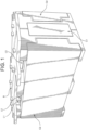
- FIG. 1 shows an external view of the coupling inductor
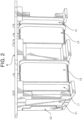
- FIG. 2 shows the coupling inductor with one of the two outer sections C2 removed.
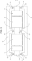
- FIG. 3 shows a relation between the central section C1 and the outer sections C2 of the core and the coils L1 to L4.
- the first coil L1 has a first number of turns N1 and is wound around the central section C1 of the core between a first end C12 and a center portion C11 of the central section C1 of the core.
- the second coil L2 has a second number of turns N2 which is larger than the first number N1 (N1 ⁇ N2), wherein the second coil L2 is wound in a direction opposite to that of the first coil L1 around the central section C1 of the core between the first end C12 and the center portion C11 of the central section C1 of the core.
- the second coil L2 is arranged such that it is tightly coupled to the first coil L1.
- the third coil L3 has a second number of turns N2 and is wound in a same direction as that of the first coil L1 around the central section C1 of the core between a second end C13 and the center portion C11 of the central section C1 of the core.
- the fourth coil L4 has the first number of turns N1.
- the fourth coil L4 is wound in a direction opposite to that of the first coil L1 around the central section C1 of the core between the second end C13 and the center portion C11 of the central section C1 of the core.
- the fourth coil L4 is arranged such that it is tightly coupled to the third coil L3.
- the central section C1 and the outer sections C2 of the core are positioned such that gaps G1 are formed between the center portion C11 of the central section C1 and center portions C21 of the outer sections C2, gaps G2 are formed between the first end C12 of the central section C1 and first ends C22 of the outer sections C2, and gaps G3 are formed between the second end C13 of the central section C1 and second ends C23 of the outer sections C2.
- the gaps G2 have a same size as the gaps G3.
- the outer sections C2 have an E-shape which has protrusions P1, P2 and P3, as shown in FIG. 3 .
- the central section C1 preferably has an I-shape, for example.
- the central section C1 may have the protrusions P1, P2 and P3.
- the coupling inductor according to the present embodiment is configured e.g. as a coupling inductor for an interleaved PFC circuit, wherein the core is configured as a ferrite core, for example.
- the coupling inductor according to the present embodiment is configured such that the first coil L1 is connected to the third coil L3 and the second coil L2 is connected to the fourth coil L4.
- connection of the first coil L1 to the third coil L3 as well as connection of the second coil L2 to the fourth coil L4 may be preferably provided via the substrate B.
- the substrate B may be a substrate dedicated for connection of coils, or may be a board for mounting another electronic device(s) thereon, such as a driving MOSFET.
- FIG. 5 shows an example of a conventional coupling inductor.
- the conventional coupling inductor according to FIG. 5 includes coils LG1 and LG2, the coil LG1 having a number of turns NG and the coil LG2 having a same number of turns as the coil LG1, wherein the coil LG1 is wound around a central section C1 of a core between a center portion C11 and a first end C12 of the central section C1 of the core, and the coil LG2 is wound in a direction opposite to that of the coil LG1 around the central section C1 of the core between the center portion C11 and a second end C13 of the central section C1 of the core.
- FIG. 6 further shows normalized values as the cross section of the central section C1 of the core, wherein the normalized values have been obtained by a cross section of the central section C1 of the core for the number of turns NG of the coils LG1 and LG2 of 40. Furthermore, FIG. 6 shows normalized values as the size of the gaps G1 to G3, wherein the normalized values have been obtained by a size of the gaps G1 to G3 for the number of turns NG of the coils LG1 and LG2 of 40.
- the cross section of central section C1 is decreased exponentially and the size of gap G1 to G3 is increased linearly, as shown in FIG. 6 .
- the gaps G1 to G3 of the conventional coupling inductor have a half size of the gaps G1 to G3 at a number of turns NG of the coils LG1 and LG2 of 40 (by a factor of 0.5).
- the central section C1 has a doubled cross section of the central section C1 of the core at the number of turns NG of the coils LG1 and LG2 of 40.
- the coupling inductor according to the present embodiment enables the magnetic flux in the core to be reduced by reducing the second number of turns N2 without increasing the magnetic resistances of the gaps G1 to G3, i.e., without increasing the gaps G1 to G3 in size.
- the coupling inductor according to the present embodiment enables the magnetic flux in the core to be reduced by adjusting the ratio of the numbers of turns of two inductors N1 : N2 which form each of the inductors, without increasing the gaps G1 to G3 in size. In this manner, it is possible to obtain compact inductors as compared to conventional coupling inductors.
- the coupling inductor according to the present embodiment demonstrates that the cross section of the central section C1 of the core and the size of the gaps G1 to G3 are changed, as shown in FIG. 8 .
- circles indicate the change in the cross section of the central section C1 of the core in the case of varying the second number of turns N2
- squares indicate the change in the size of the gaps G1-G3 in the case of varying the second number of turns N2.
- FIG. 8 further shows normalized values as the cross section of the central section C1 of the core, wherein the normalized values have been obtained by a cross section of the central section C1 of the core for the second number of turns N2 of 40 (i.e., in the case where the first number of turns N1 is zero and each of two inductors is thus configured in a same manner as a conventional coupling inductor which is formed by a single coil).
- FIG. 8 shows normalized values as the size of the gaps G1 to G3, wherein the normalized values have been obtained by a size of the gaps G1 to G3 for the second number of turns N2 of 40.
- the coupling inductor according to the present embodiment enables the size of the gaps G1 to G3 to be reduced by reducing the second number of turns N2, as shown in FIG. 8 .
- the cross section of the central section C1 of the core of the coupling inductor according to the present embodiment is only slightly increased.
- the gaps G1 to G3 have a half size of the gaps G1 to G3 at the second number of turns N2 of 40 (by a factor of 0.5).
- the central section C1 of the core has a size which is only 1.15 times as large as a cross section of the central section C1 of the core for the second number of turns N2 of 40.
Landscapes
- Engineering & Computer Science (AREA)
- Power Engineering (AREA)
- Chemical & Material Sciences (AREA)
- Composite Materials (AREA)
- Microelectronics & Electronic Packaging (AREA)
- Coils Or Transformers For Communication (AREA)
Abstract
Description
- The present invention relates to a coupling inductor.
- An on-board charger for a vehicle is equipped with an interleaved PFC (power factor correction) circuit in order to efficiently convert a high AC electric power into a DC power. Such an interleaved PFC circuit necessitates two inductors. For the reason of the need for compact on-board chargers, it is desired to provide more compact inductors.
- Therefore, an interleaved PFC circuit with a coupling inductor is proposed (for example Patent Document 1). The coupling inductor is formed by two coils wound around a core with opposite polarities so that magnetic fluxes generated by the two coils cancel each other and magnetic flux in the core is thus reduced. In this manner, the coupling inductor enables the core to be reduced in size, i.e., more compact inductors to be obtained.
- Patent Document 1:
JP 2015-201642 A - In the case where a coupling inductor is used for a PFC circuit, it is not possible to use a dust core as the core for the coupling inductor because a ripple current with a doubled operating frequency flows therethrough. For this reason, a ferrite core is usually used in the coupling inductor for a PFC circuit. A ferrite core has a small saturation magnetic flux density, which is 1/3 of the saturation magnetic flux density of the dust core.
- Therefore,
Patent Document 1 discloses that magnetic saturation is avoided by providing a plurality of gap in core of a coupling inductor. However, it is difficult to dissipate heat from a coupling inductor having the above-described configuration. In addition, such a coupling inductor requires an accuracy for assembly. Therefore, the technique disclosed inPatent Document 1 is not practical. - Therefore, an objective of the present invention is to provide a compact coupling inductor.
- In order to achieve the above-mentioned objective, a coupling inductor according to the present invention includes a core having a central section and an outer section, a first coil wound around the central section between a first end and a center portion of the central section, a second coil wound around the central section between the first end and the center portion of the central section, wherein the second coil is wound in a direction opposite to a direction in which the first coil is wound, a third coil connected to the first coil and wound around the central section between a second end and the center portion of the central section, wherein the third coil is wound in a same direction as the direction in which the first coil is wound, and a fourth coil connected to the second coil and wound around the central section between the second end and the center portion of the central section, wherein the fourth coil is wound in a direction opposite to the direction in which the first coil is wound.
- The present invention enables a compact coupling inductor to be provided.
-
-
FIG. 1 shows an exterior view of a coupling inductor according to an embodiment of the present invention; -
FIG. 2 shows the coupling inductor with one of two outer sections C2 removed; -
FIG. 3 shows a relation between a central section C1 and the outer sections C22 of a core as well as coils L1-L4; -
FIG. 4A shows a connection relation between the coils L1-L4; -
FIG. 4B shows a connection relation between the coils L1-L4; -
FIG. 5 shows an example of a conventional coupling inductor; -
FIG. 6 shows changes of the central section C1 of the core in its cross section and in size of gaps G1-G3 in the case of varying a number of turns NG for coils LG1 and LG2 in the conventional coupling inductor; -
FIG. 7 shows an equivalent magnetic circuit for the coupling inductor according to the embodiment of the present invention; and -
FIG. 8 shows changes of the central section C1 of the core in its cross section and in size of gaps G1-G3 in the case of varying a second number of turns N2 in the coupling inductor according to the embodiment of the present invention. - As shown in
FIGS. 1 to 3 , a coupling inductor according to an embodiment of the present invention includes a core having a central section C1 and two outer sections C2, a first coil L1, a second coil L2, a third coil L3, a fourth coil L4, and a substrate B.FIG. 1 shows an external view of the coupling inductor, andFIG. 2 shows the coupling inductor with one of the two outer sections C2 removed.FIG. 3 shows a relation between the central section C1 and the outer sections C2 of the core and the coils L1 to L4. - The first coil L1 has a first number of turns N1 and is wound around the central section C1 of the core between a first end C12 and a center portion C11 of the central section C1 of the core.
- The second coil L2 has a second number of turns N2 which is larger than the first number N1 (N1 < N2), wherein the second coil L2 is wound in a direction opposite to that of the first coil L1 around the central section C1 of the core between the first end C12 and the center portion C11 of the central section C1 of the core. For example, the second coil L2 is arranged such that it is tightly coupled to the first coil L1.
- The third coil L3 has a second number of turns N2 and is wound in a same direction as that of the first coil L1 around the central section C1 of the core between a second end C13 and the center portion C11 of the central section C1 of the core.
- The fourth coil L4 has the first number of turns N1. The fourth coil L4 is wound in a direction opposite to that of the first coil L1 around the central section C1 of the core between the second end C13 and the center portion C11 of the central section C1 of the core. For example, the fourth coil L4 is arranged such that it is tightly coupled to the third coil L3.
- The central section C1 and the outer sections C2 of the core are positioned such that gaps G1 are formed between the center portion C11 of the central section C1 and center portions C21 of the outer sections C2, gaps G2 are formed between the first end C12 of the central section C1 and first ends C22 of the outer sections C2, and gaps G3 are formed between the second end C13 of the central section C1 and second ends C23 of the outer sections C2. The gaps G2 have a same size as the gaps G3.
- Preferably, the outer sections C2 have an E-shape which has protrusions P1, P2 and P3, as shown in
FIG. 3 . In the case of the outer sections C2 having an E-shape, the central section C1 preferably has an I-shape, for example. Instead of the outer sections C2, the central section C1 may have the protrusions P1, P2 and P3. - The coupling inductor according to the present embodiment is configured e.g. as a coupling inductor for an interleaved PFC circuit, wherein the core is configured as a ferrite core, for example. As shown in
FIG. 4A , the coupling inductor according to the present embodiment is configured such that the first coil L1 is connected to the third coil L3 and the second coil L2 is connected to the fourth coil L4. In this manner, the coupling inductor according to the present embodiment forms a coupling inductor including inductors with a number of turns N (= N1 + N2) which are formed by the first coil L1 and the third coil L3 and by the second coil L2 and the fourth coil L4, respectively, as shown inFIG. 4B . - For example, connection of the first coil L1 to the third coil L3 as well as connection of the second coil L2 to the fourth coil L4 may be preferably provided via the substrate B. The substrate B may be a substrate dedicated for connection of coils, or may be a board for mounting another electronic device(s) thereon, such as a driving MOSFET.
-
FIG. 5 shows an example of a conventional coupling inductor. Instead of the coils L1 to L4 of the coupling inductor according to the above-described embodiment, the conventional coupling inductor according toFIG. 5 includes coils LG1 and LG2, the coil LG1 having a number of turns NG and the coil LG2 having a same number of turns as the coil LG1, wherein the coil LG1 is wound around a central section C1 of a core between a center portion C11 and a first end C12 of the central section C1 of the core, and the coil LG2 is wound in a direction opposite to that of the coil LG1 around the central section C1 of the core between the center portion C11 and a second end C13 of the central section C1 of the core. - In order to reduce the coils LG1 and LG2 in size (i.e., a cross section of the central section C1 of the core) while maintaining parameters related to an electrical performance such as a ripple current in the conventional coupling inductor according to
FIG. 5 , it is necessary to increase the number of turns of the coils LG1 and LG2. If the coils LG1 and LG2 are reduced in size and the number of turns of the coils LG1 and LG2 are increased, this causes an abrupt increase of a magnetic flux density through the core. In this case, in order to prevent the magnetic flux density through the core from exceeding a saturation magnetic flux density of the core, it is necessary to increase the gaps G1 to G3 in size and thus increase magnetic resistances of the gaps G1 to G3. In other words, for reducing the cross section of the central section C1 of the core in the conventional coupling inductor, it is necessary to increase the gaps G1 to G3 in size. As a result, the conventional coupling inductor is difficult to be made compact as a whole. - For determining the parameters related to the electrical performance such as ripple current and for the sake of simplicity, all the gaps G1 to G3 shall have a same size. Under this condition, if the number of turns NG of the coil LG1, LG2 is varied, the conventional coupling inductor demonstrates that the cross section of the central section C1 of the core and the size of the gaps G1 to G3 are changed, as shown in
FIG. 6 . InFIG. 6 , circles indicate the change in the cross section of the central section C1 of the core, and squares indicate the change in the size of the gaps G1-G3.FIG. 6 further shows normalized values as the cross section of the central section C1 of the core, wherein the normalized values have been obtained by a cross section of the central section C1 of the core for the number of turns NG of the coils LG1 and LG2 of 40. Furthermore,FIG. 6 shows normalized values as the size of the gaps G1 to G3, wherein the normalized values have been obtained by a size of the gaps G1 to G3 for the number of turns NG of the coils LG1 and LG2 of 40. - In the conventional coupling inductor, as the number of turns NG of the coils LG1 and LG2 is increased, the cross section of central section C1 is decreased exponentially and the size of gap G1 to G3 is increased linearly, as shown in
FIG. 6 . For a number of turns NG of the coils LG1 and LG2 of 20, the gaps G1 to G3 of the conventional coupling inductor have a half size of the gaps G1 to G3 at a number of turns NG of the coils LG1 and LG2 of 40 (by a factor of 0.5). Furthermore, for the number of turns of 20, the central section C1 has a doubled cross section of the central section C1 of the core at the number of turns NG of the coils LG1 and LG2 of 40. - On the other hand, the coupling inductor according to the present embodiment includes two inductors which are each formed by two coils, wherein each of the two coils of one inductor is magnetically coupled to one of the coils of the other inductor. Therefore, the coupling inductor according to the present embodiment enables the magnetic flux through the core to be adjusted by varying a ratio of the numbers of turns N1 : N2 of the two coils which form each of the two inductors, wherein the adjustment can be accomplished without changing the individual numbers of turns N of the two inductors (N = N1 + N2).
-
FIG. 7 shows an equivalent magnetic circuit of the coupling inductor according to the present embodiment. If the first coil L1 and the second coil L2 are tightly coupled to each other and the third coil L3 and the fourth coil L4 are tightly coupled to each other, a magnetic flux ϕc through a magnetic resistance of the gap G1 and a magnetic flux ϕw through magnetic resistances of the gaps G2, G3, i.e., DC components of a magnetic flux in the core, are obtained according to the following formula:
- This means that the coupling inductor according to the present embodiment enables the magnetic flux in the core to be reduced by reducing the second number of turns N2 without increasing the magnetic resistances of the gaps G1 to G3, i.e., without increasing the gaps G1 to G3 in size. This means that the coupling inductor according to the present embodiment enables the magnetic flux in the core to be reduced by adjusting the ratio of the numbers of turns of two inductors N1 : N2 which form each of the inductors, without increasing the gaps G1 to G3 in size. In this manner, it is possible to obtain compact inductors as compared to conventional coupling inductors.
- Under the same condition as in
FIG. 6 , if the ratio of the numbers of turns N1 : N2 of two inductors which form the inductor together is varied while maintaining a constant number of turns N of the inductor (N = N1 + N2), the coupling inductor according to the present embodiment demonstrates that the cross section of the central section C1 of the core and the size of the gaps G1 to G3 are changed, as shown inFIG. 8 . InFIG. 8 , circles indicate the change in the cross section of the central section C1 of the core in the case of varying the second number of turns N2, and squares indicate the change in the size of the gaps G1-G3 in the case of varying the second number of turns N2.FIG. 8 further shows normalized values as the cross section of the central section C1 of the core, wherein the normalized values have been obtained by a cross section of the central section C1 of the core for the second number of turns N2 of 40 (i.e., in the case where the first number of turns N1 is zero and each of two inductors is thus configured in a same manner as a conventional coupling inductor which is formed by a single coil). Furthermore,FIG. 8 shows normalized values as the size of the gaps G1 to G3, wherein the normalized values have been obtained by a size of the gaps G1 to G3 for the second number of turns N2 of 40. - The coupling inductor according to the present embodiment enables the size of the gaps G1 to G3 to be reduced by reducing the second number of turns N2, as shown in
FIG. 8 . Even when the second number of turns N2 is reduced, the cross section of the central section C1 of the core of the coupling inductor according to the present embodiment is only slightly increased. In the example ofFIG. 8 , for the second number of turns N2 of 30, the gaps G1 to G3 have a half size of the gaps G1 to G3 at the second number of turns N2 of 40 (by a factor of 0.5). In this case, the central section C1 of the core has a size which is only 1.15 times as large as a cross section of the central section C1 of the core for the second number of turns N2 of 40. This means that the coupling inductor according to the present embodiment enables inductors to be compact as compared with the conventional coupling inductor. - The present invention has been described above by means of the preferable embodiment thereof. Although the invention has been described herein by presenting a specific example, various modifications and changes may be made to such an example without departing from the spirit and scope of the invention as set forth in the claims.
-
- C1
- Central section of a core
- C11
- Center portion of the central section C1 of the core
- C12
- First end of the central section C1 of the core
- C13
- Second end of the central section C1 of the core
- C2
- Outer section of the core
- C21
- Center portions of the outer sections C2 of the core
- C22
- First ends of the outer sections C2 of the core
- C23
- Second ends of the outer sections C2 of the core
- L1
- First coil
- L2
- Second coil
- L3
- Third coil
- L4
- Fourth coil
- G1-G3
- Gaps
- B
- Substrate
Claims (7)
- A coupling inductor comprising:a core having a central section (C1) and an outer section (C2);a first coil (L1) wound around the central section (C1) between a first end (C12) and a center portion (C11) of the central section (C1);a second coil (L2) wound around the central section (C1) between the first end (C12) and the center portion (C11) of the central section (C1), wherein the second coil (L2) is wound in a direction opposite to a direction in which the first coil (L1) is wound;a third coil (L3) connected to the first coil (L1) and wound around the central section (C1) between a second end (C13) and the center portion (C11) of the central section (C1), wherein the third coil (L3) is wound in a same direction as the direction in which the first coil (L1) is wound; anda fourth coil (L4) connected to the second coil (L2) and wound around the central section (C1) between the second end (C13) and the center portion (C11) of the central section (C1), wherein the fourth coil (L4) is wound in a direction opposite to the direction in which the first coil (L1) is wound.
- The coupling inductor according to claim 1,
wherein the central section (C1) and the outer section (C2) are positioned such that a gap (G1) exists between the center portion (C11) of the central section (C1) and a center portion (C21) of the outer section (C2), a gap (G2) exists between the first end (C12) of the central section (C1) and a first end (C22) of the outer section (C2), and a gap (G3) exists between the second end (C13) of the central section (C1) and a second end (C23) of the outer section (C2). - The coupling inductor according to claim 2,
wherein the central section (C1) has an I-shape and the outer section (C2) has an E-shape. - The coupling inductor according to any one of claims 1 to 3,
wherein connection of the first coil (L1) and the third coil (L3) as well as connection of the second coil (L2) and the fourth coil (L4) are provided via a substrate (B). - The coupling inductor according to any one of claims 1 to 4,wherein the coupling inductor is configured as a coupling inductor for an interleaved PFC circuit, andwherein the core is configured as a ferrite core.
- The coupling inductor according to any one of claims 1 to 5,
wherein the first coil (L1) and the second coil (L2) are tightly coupled to each other. - The coupling inductor according to any one of claims 1 to 6,
wherein the third coil (L3) and the fourth coil (L4) are tightly coupled to each other.
Applications Claiming Priority (1)
| Application Number | Priority Date | Filing Date | Title |
|---|---|---|---|
| JP2021151752A JP7451469B2 (en) | 2021-09-17 | 2021-09-17 | coupled inductor |
Publications (2)
| Publication Number | Publication Date |
|---|---|
| EP4152353A1 true EP4152353A1 (en) | 2023-03-22 |
| EP4152353B1 EP4152353B1 (en) | 2024-04-10 |
Family
ID=83005909
Family Applications (1)
| Application Number | Title | Priority Date | Filing Date |
|---|---|---|---|
| EP22191446.8A Active EP4152353B1 (en) | 2021-09-17 | 2022-08-22 | Coupling inductor |
Country Status (4)
| Country | Link |
|---|---|
| US (1) | US20230091183A1 (en) |
| EP (1) | EP4152353B1 (en) |
| JP (1) | JP7451469B2 (en) |
| CN (1) | CN115831558A (en) |
Citations (4)
| Publication number | Priority date | Publication date | Assignee | Title |
|---|---|---|---|---|
| JP2015201642A (en) | 2014-04-03 | 2015-11-12 | スミダ・コンポーネンツ・アンド・モジュールズ・ゲゼルシャフト・ミット・ベシュレンクテル・ハフツング | choke |
| CN104410257B (en) * | 2014-12-23 | 2017-12-15 | 湘潭大学 | A kind of passive element integrating device of LCL filter |
| JP2021019030A (en) * | 2019-07-18 | 2021-02-15 | 矢崎総業株式会社 | Magnetic coupling type inductor |
| WO2021168797A1 (en) * | 2020-02-28 | 2021-09-02 | Telefonaktiebolaget Lm Ericsson (Publ) | Common mode choke |
Family Cites Families (19)
| Publication number | Priority date | Publication date | Assignee | Title |
|---|---|---|---|---|
| US3681725A (en) * | 1969-08-25 | 1972-08-01 | Denki Onkyo Co Ltd | Saturable reactor for correcting raster distortion |
| JPS62197824U (en) * | 1986-06-05 | 1987-12-16 | ||
| JP3501670B2 (en) * | 1998-12-18 | 2004-03-02 | 東大無線株式会社 | Trance |
| JP2004335886A (en) * | 2003-05-09 | 2004-11-25 | Canon Inc | Transformer assembly, power conversion device and solar power generation device using the same |
| TWM267603U (en) * | 2004-07-16 | 2005-06-11 | Logah Technology Corp | Anti-interference transformer |
| US20080211615A1 (en) * | 2005-09-29 | 2008-09-04 | Greatchip Technology Co., Ltd. | Inverter transformer |
| JP2007180129A (en) * | 2005-12-27 | 2007-07-12 | Shindengen Electric Mfg Co Ltd | Transformer |
| WO2009104221A1 (en) * | 2008-02-22 | 2009-08-27 | 田淵電機株式会社 | Reactor |
| JP2010016234A (en) * | 2008-07-04 | 2010-01-21 | Hitachi Ferrite Electronics Ltd | Choke coil for interleave-controlled power factor correction circuit |
| US20100019875A1 (en) * | 2008-07-25 | 2010-01-28 | Ampower Technology Co., Ltd. | High voltage transformer employed in an inverter |
| CN201298430Y (en) * | 2008-09-26 | 2009-08-26 | 国琏电子(上海)有限公司 | transformer |
| JP5062439B2 (en) * | 2009-04-28 | 2012-10-31 | Tdk株式会社 | PFC choke coil for interleaving |
| EP2771891B2 (en) * | 2011-10-25 | 2021-03-24 | BRUSA Elektronik AG | Inductive component and use |
| KR101428199B1 (en) * | 2012-10-22 | 2014-08-07 | 엘지이노텍 주식회사 | The common mode filter and the power supply device having the same |
| JP6619926B2 (en) * | 2014-09-25 | 2019-12-11 | 本田技研工業株式会社 | Combined reactor |
| JP6417206B2 (en) * | 2014-12-19 | 2018-10-31 | 株式会社豊田自動織機 | Power converter |
| US9874897B2 (en) * | 2016-05-03 | 2018-01-23 | Toyota Motor Engineering & Manufacturing North America, Inc. | Integrated inductor |
| JP2019204945A (en) * | 2018-05-18 | 2019-11-28 | Ntn株式会社 | Coupling inductor and switching circuit |
| JP7373119B2 (en) * | 2020-02-19 | 2023-11-02 | スミダコーポレーション株式会社 | magnetically coupled inductor |
-
2021
- 2021-09-17 JP JP2021151752A patent/JP7451469B2/en active Active
-
2022
- 2022-08-15 US US17/887,863 patent/US20230091183A1/en active Pending
- 2022-08-22 EP EP22191446.8A patent/EP4152353B1/en active Active
- 2022-09-02 CN CN202211072861.1A patent/CN115831558A/en not_active Withdrawn
Patent Citations (4)
| Publication number | Priority date | Publication date | Assignee | Title |
|---|---|---|---|---|
| JP2015201642A (en) | 2014-04-03 | 2015-11-12 | スミダ・コンポーネンツ・アンド・モジュールズ・ゲゼルシャフト・ミット・ベシュレンクテル・ハフツング | choke |
| CN104410257B (en) * | 2014-12-23 | 2017-12-15 | 湘潭大学 | A kind of passive element integrating device of LCL filter |
| JP2021019030A (en) * | 2019-07-18 | 2021-02-15 | 矢崎総業株式会社 | Magnetic coupling type inductor |
| WO2021168797A1 (en) * | 2020-02-28 | 2021-09-02 | Telefonaktiebolaget Lm Ericsson (Publ) | Common mode choke |
Also Published As
| Publication number | Publication date |
|---|---|
| CN115831558A (en) | 2023-03-21 |
| JP2023043973A (en) | 2023-03-30 |
| JP7451469B2 (en) | 2024-03-18 |
| EP4152353B1 (en) | 2024-04-10 |
| US20230091183A1 (en) | 2023-03-23 |
Similar Documents
| Publication | Publication Date | Title |
|---|---|---|
| US11251713B2 (en) | Multiple parallel-connected resonant converter, inductor-integrated magnetic element and transformer-integrated magnetic element | |
| US10211745B2 (en) | Resonant LLC converter with a multi-leg transformer with gapped center leg | |
| US5619400A (en) | Magnetic core structures and construction techniques therefor | |
| JPH05299270A (en) | Electromagnetic device and electromagnetic core structure | |
| CN114823083B (en) | Integrated magnetic components | |
| CN101578672A (en) | Shared reactor transformer | |
| KR100754055B1 (en) | Split inductor with partial turn of each winding and PCC containing such inductor | |
| US11205537B2 (en) | Magnetic component, resonant electrical circuit, electrical converter and electrical system | |
| CN104025213A (en) | Inductive component and use | |
| JP6953920B2 (en) | Magnetic composite parts | |
| JP2007059507A (en) | Transformer for board mounting | |
| US12387871B2 (en) | Leakage transformer | |
| US6100781A (en) | High leakage inductance transformer | |
| US6985063B2 (en) | Transformer core | |
| EP4152353B1 (en) | Coupling inductor | |
| US20090109717A1 (en) | Power factor corrected circuit having integrated coil | |
| EP3739601B1 (en) | Interleaved llc converter | |
| US20080030283A1 (en) | Circuit, Manufacturing Method And Inverter circuit For Discharge Tube | |
| US20190313531A1 (en) | Inductively balanced power supply circuit and method of manufacture | |
| US20180040408A1 (en) | Reactor | |
| CN118553509B (en) | A transformer for naturally canceling common-mode noise of a power converter with symmetrical noise sources | |
| JP2007317892A (en) | Multilayer inductor | |
| JPS5934608A (en) | Core for small sized reactor | |
| EP4621811A1 (en) | High power high current transformer | |
| US12488929B2 (en) | Magnetic apparatus, and voltage converter including the same |
Legal Events
| Date | Code | Title | Description |
|---|---|---|---|
| PUAI | Public reference made under article 153(3) epc to a published international application that has entered the european phase |
Free format text: ORIGINAL CODE: 0009012 |
|
| STAA | Information on the status of an ep patent application or granted ep patent |
Free format text: STATUS: REQUEST FOR EXAMINATION WAS MADE |
|
| 17P | Request for examination filed |
Effective date: 20220822 |
|
| AK | Designated contracting states |
Kind code of ref document: A1 Designated state(s): AL AT BE BG CH CY CZ DE DK EE ES FI FR GB GR HR HU IE IS IT LI LT LU LV MC MK MT NL NO PL PT RO RS SE SI SK SM TR |
|
| RAP3 | Party data changed (applicant data changed or rights of an application transferred) |
Owner name: YAZAKI CORPORATION |
|
| RBV | Designated contracting states (corrected) |
Designated state(s): AL AT BE BG CH CY CZ DE DK EE ES FI FR GB GR HR HU IE IS IT LI LT LU LV MC MK MT NL NO PL PT RO RS SE SI SK SM TR |
|
| STAA | Information on the status of an ep patent application or granted ep patent |
Free format text: STATUS: EXAMINATION IS IN PROGRESS |
|
| 17Q | First examination report despatched |
Effective date: 20230810 |
|
| GRAP | Despatch of communication of intention to grant a patent |
Free format text: ORIGINAL CODE: EPIDOSNIGR1 |
|
| STAA | Information on the status of an ep patent application or granted ep patent |
Free format text: STATUS: GRANT OF PATENT IS INTENDED |
|
| INTG | Intention to grant announced |
Effective date: 20240202 |
|
| GRAS | Grant fee paid |
Free format text: ORIGINAL CODE: EPIDOSNIGR3 |
|
| GRAA | (expected) grant |
Free format text: ORIGINAL CODE: 0009210 |
|
| STAA | Information on the status of an ep patent application or granted ep patent |
Free format text: STATUS: THE PATENT HAS BEEN GRANTED |
|
| AK | Designated contracting states |
Kind code of ref document: B1 Designated state(s): AL AT BE BG CH CY CZ DE DK EE ES FI FR GB GR HR HU IE IS IT LI LT LU LV MC MK MT NL NO PL PT RO RS SE SI SK SM TR |
|
| REG | Reference to a national code |
Ref country code: GB Ref legal event code: FG4D |
|
| REG | Reference to a national code |
Ref country code: CH Ref legal event code: EP |
|
| REG | Reference to a national code |
Ref country code: DE Ref legal event code: R096 Ref document number: 602022002803 Country of ref document: DE |
|
| REG | Reference to a national code |
Ref country code: IE Ref legal event code: FG4D |
|
| REG | Reference to a national code |
Ref country code: LT Ref legal event code: MG9D |
|
| REG | Reference to a national code |
Ref country code: NL Ref legal event code: MP Effective date: 20240410 |
|
| REG | Reference to a national code |
Ref country code: AT Ref legal event code: MK05 Ref document number: 1675789 Country of ref document: AT Kind code of ref document: T Effective date: 20240410 |
|
| PG25 | Lapsed in a contracting state [announced via postgrant information from national office to epo] |
Ref country code: NL Free format text: LAPSE BECAUSE OF FAILURE TO SUBMIT A TRANSLATION OF THE DESCRIPTION OR TO PAY THE FEE WITHIN THE PRESCRIBED TIME-LIMIT Effective date: 20240410 |
|
| PG25 | Lapsed in a contracting state [announced via postgrant information from national office to epo] |
Ref country code: NL Free format text: LAPSE BECAUSE OF FAILURE TO SUBMIT A TRANSLATION OF THE DESCRIPTION OR TO PAY THE FEE WITHIN THE PRESCRIBED TIME-LIMIT Effective date: 20240410 |
|
| PG25 | Lapsed in a contracting state [announced via postgrant information from national office to epo] |
Ref country code: IS Free format text: LAPSE BECAUSE OF FAILURE TO SUBMIT A TRANSLATION OF THE DESCRIPTION OR TO PAY THE FEE WITHIN THE PRESCRIBED TIME-LIMIT Effective date: 20240810 |
|
| PG25 | Lapsed in a contracting state [announced via postgrant information from national office to epo] |
Ref country code: BG Free format text: LAPSE BECAUSE OF FAILURE TO SUBMIT A TRANSLATION OF THE DESCRIPTION OR TO PAY THE FEE WITHIN THE PRESCRIBED TIME-LIMIT Effective date: 20240410 |
|
| PG25 | Lapsed in a contracting state [announced via postgrant information from national office to epo] |
Ref country code: FI Free format text: LAPSE BECAUSE OF FAILURE TO SUBMIT A TRANSLATION OF THE DESCRIPTION OR TO PAY THE FEE WITHIN THE PRESCRIBED TIME-LIMIT Effective date: 20240410 Ref country code: HR Free format text: LAPSE BECAUSE OF FAILURE TO SUBMIT A TRANSLATION OF THE DESCRIPTION OR TO PAY THE FEE WITHIN THE PRESCRIBED TIME-LIMIT Effective date: 20240410 |
|
| PG25 | Lapsed in a contracting state [announced via postgrant information from national office to epo] |
Ref country code: GR Free format text: LAPSE BECAUSE OF FAILURE TO SUBMIT A TRANSLATION OF THE DESCRIPTION OR TO PAY THE FEE WITHIN THE PRESCRIBED TIME-LIMIT Effective date: 20240711 |
|
| PG25 | Lapsed in a contracting state [announced via postgrant information from national office to epo] |
Ref country code: PT Free format text: LAPSE BECAUSE OF FAILURE TO SUBMIT A TRANSLATION OF THE DESCRIPTION OR TO PAY THE FEE WITHIN THE PRESCRIBED TIME-LIMIT Effective date: 20240812 |
|
| PG25 | Lapsed in a contracting state [announced via postgrant information from national office to epo] |
Ref country code: ES Free format text: LAPSE BECAUSE OF FAILURE TO SUBMIT A TRANSLATION OF THE DESCRIPTION OR TO PAY THE FEE WITHIN THE PRESCRIBED TIME-LIMIT Effective date: 20240410 |
|
| PG25 | Lapsed in a contracting state [announced via postgrant information from national office to epo] |
Ref country code: AT Free format text: LAPSE BECAUSE OF FAILURE TO SUBMIT A TRANSLATION OF THE DESCRIPTION OR TO PAY THE FEE WITHIN THE PRESCRIBED TIME-LIMIT Effective date: 20240410 |
|
| PG25 | Lapsed in a contracting state [announced via postgrant information from national office to epo] |
Ref country code: PL Free format text: LAPSE BECAUSE OF FAILURE TO SUBMIT A TRANSLATION OF THE DESCRIPTION OR TO PAY THE FEE WITHIN THE PRESCRIBED TIME-LIMIT Effective date: 20240410 |
|
| PG25 | Lapsed in a contracting state [announced via postgrant information from national office to epo] |
Ref country code: LV Free format text: LAPSE BECAUSE OF FAILURE TO SUBMIT A TRANSLATION OF THE DESCRIPTION OR TO PAY THE FEE WITHIN THE PRESCRIBED TIME-LIMIT Effective date: 20240410 |
|
| PG25 | Lapsed in a contracting state [announced via postgrant information from national office to epo] |
Ref country code: PT Free format text: LAPSE BECAUSE OF FAILURE TO SUBMIT A TRANSLATION OF THE DESCRIPTION OR TO PAY THE FEE WITHIN THE PRESCRIBED TIME-LIMIT Effective date: 20240812 Ref country code: PL Free format text: LAPSE BECAUSE OF FAILURE TO SUBMIT A TRANSLATION OF THE DESCRIPTION OR TO PAY THE FEE WITHIN THE PRESCRIBED TIME-LIMIT Effective date: 20240410 Ref country code: NO Free format text: LAPSE BECAUSE OF FAILURE TO SUBMIT A TRANSLATION OF THE DESCRIPTION OR TO PAY THE FEE WITHIN THE PRESCRIBED TIME-LIMIT Effective date: 20240710 Ref country code: LV Free format text: LAPSE BECAUSE OF FAILURE TO SUBMIT A TRANSLATION OF THE DESCRIPTION OR TO PAY THE FEE WITHIN THE PRESCRIBED TIME-LIMIT Effective date: 20240410 Ref country code: IS Free format text: LAPSE BECAUSE OF FAILURE TO SUBMIT A TRANSLATION OF THE DESCRIPTION OR TO PAY THE FEE WITHIN THE PRESCRIBED TIME-LIMIT Effective date: 20240810 Ref country code: HR Free format text: LAPSE BECAUSE OF FAILURE TO SUBMIT A TRANSLATION OF THE DESCRIPTION OR TO PAY THE FEE WITHIN THE PRESCRIBED TIME-LIMIT Effective date: 20240410 Ref country code: GR Free format text: LAPSE BECAUSE OF FAILURE TO SUBMIT A TRANSLATION OF THE DESCRIPTION OR TO PAY THE FEE WITHIN THE PRESCRIBED TIME-LIMIT Effective date: 20240711 Ref country code: FI Free format text: LAPSE BECAUSE OF FAILURE TO SUBMIT A TRANSLATION OF THE DESCRIPTION OR TO PAY THE FEE WITHIN THE PRESCRIBED TIME-LIMIT Effective date: 20240410 Ref country code: ES Free format text: LAPSE BECAUSE OF FAILURE TO SUBMIT A TRANSLATION OF THE DESCRIPTION OR TO PAY THE FEE WITHIN THE PRESCRIBED TIME-LIMIT Effective date: 20240410 Ref country code: BG Free format text: LAPSE BECAUSE OF FAILURE TO SUBMIT A TRANSLATION OF THE DESCRIPTION OR TO PAY THE FEE WITHIN THE PRESCRIBED TIME-LIMIT Effective date: 20240410 Ref country code: AT Free format text: LAPSE BECAUSE OF FAILURE TO SUBMIT A TRANSLATION OF THE DESCRIPTION OR TO PAY THE FEE WITHIN THE PRESCRIBED TIME-LIMIT Effective date: 20240410 Ref country code: RS Free format text: LAPSE BECAUSE OF FAILURE TO SUBMIT A TRANSLATION OF THE DESCRIPTION OR TO PAY THE FEE WITHIN THE PRESCRIBED TIME-LIMIT Effective date: 20240710 |
|
| REG | Reference to a national code |
Ref country code: DE Ref legal event code: R097 Ref document number: 602022002803 Country of ref document: DE |
|
| PG25 | Lapsed in a contracting state [announced via postgrant information from national office to epo] |
Ref country code: DK Free format text: LAPSE BECAUSE OF FAILURE TO SUBMIT A TRANSLATION OF THE DESCRIPTION OR TO PAY THE FEE WITHIN THE PRESCRIBED TIME-LIMIT Effective date: 20240410 |
|
| PG25 | Lapsed in a contracting state [announced via postgrant information from national office to epo] |
Ref country code: EE Free format text: LAPSE BECAUSE OF FAILURE TO SUBMIT A TRANSLATION OF THE DESCRIPTION OR TO PAY THE FEE WITHIN THE PRESCRIBED TIME-LIMIT Effective date: 20240410 |
|
| PG25 | Lapsed in a contracting state [announced via postgrant information from national office to epo] |
Ref country code: CZ Free format text: LAPSE BECAUSE OF FAILURE TO SUBMIT A TRANSLATION OF THE DESCRIPTION OR TO PAY THE FEE WITHIN THE PRESCRIBED TIME-LIMIT Effective date: 20240410 |
|
| PG25 | Lapsed in a contracting state [announced via postgrant information from national office to epo] |
Ref country code: SK Free format text: LAPSE BECAUSE OF FAILURE TO SUBMIT A TRANSLATION OF THE DESCRIPTION OR TO PAY THE FEE WITHIN THE PRESCRIBED TIME-LIMIT Effective date: 20240410 Ref country code: RO Free format text: LAPSE BECAUSE OF FAILURE TO SUBMIT A TRANSLATION OF THE DESCRIPTION OR TO PAY THE FEE WITHIN THE PRESCRIBED TIME-LIMIT Effective date: 20240410 |
|
| PG25 | Lapsed in a contracting state [announced via postgrant information from national office to epo] |
Ref country code: SM Free format text: LAPSE BECAUSE OF FAILURE TO SUBMIT A TRANSLATION OF THE DESCRIPTION OR TO PAY THE FEE WITHIN THE PRESCRIBED TIME-LIMIT Effective date: 20240410 |
|
| PG25 | Lapsed in a contracting state [announced via postgrant information from national office to epo] |
Ref country code: SM Free format text: LAPSE BECAUSE OF FAILURE TO SUBMIT A TRANSLATION OF THE DESCRIPTION OR TO PAY THE FEE WITHIN THE PRESCRIBED TIME-LIMIT Effective date: 20240410 Ref country code: SK Free format text: LAPSE BECAUSE OF FAILURE TO SUBMIT A TRANSLATION OF THE DESCRIPTION OR TO PAY THE FEE WITHIN THE PRESCRIBED TIME-LIMIT Effective date: 20240410 Ref country code: RO Free format text: LAPSE BECAUSE OF FAILURE TO SUBMIT A TRANSLATION OF THE DESCRIPTION OR TO PAY THE FEE WITHIN THE PRESCRIBED TIME-LIMIT Effective date: 20240410 Ref country code: EE Free format text: LAPSE BECAUSE OF FAILURE TO SUBMIT A TRANSLATION OF THE DESCRIPTION OR TO PAY THE FEE WITHIN THE PRESCRIBED TIME-LIMIT Effective date: 20240410 Ref country code: DK Free format text: LAPSE BECAUSE OF FAILURE TO SUBMIT A TRANSLATION OF THE DESCRIPTION OR TO PAY THE FEE WITHIN THE PRESCRIBED TIME-LIMIT Effective date: 20240410 Ref country code: CZ Free format text: LAPSE BECAUSE OF FAILURE TO SUBMIT A TRANSLATION OF THE DESCRIPTION OR TO PAY THE FEE WITHIN THE PRESCRIBED TIME-LIMIT Effective date: 20240410 |
|
| PG25 | Lapsed in a contracting state [announced via postgrant information from national office to epo] |
Ref country code: IT Free format text: LAPSE BECAUSE OF FAILURE TO SUBMIT A TRANSLATION OF THE DESCRIPTION OR TO PAY THE FEE WITHIN THE PRESCRIBED TIME-LIMIT Effective date: 20240410 |
|
| PLBE | No opposition filed within time limit |
Free format text: ORIGINAL CODE: 0009261 |
|
| STAA | Information on the status of an ep patent application or granted ep patent |
Free format text: STATUS: NO OPPOSITION FILED WITHIN TIME LIMIT |
|
| 26N | No opposition filed |
Effective date: 20250113 |
|
| PG25 | Lapsed in a contracting state [announced via postgrant information from national office to epo] |
Ref country code: LU Free format text: LAPSE BECAUSE OF NON-PAYMENT OF DUE FEES Effective date: 20240822 |
|
| PG25 | Lapsed in a contracting state [announced via postgrant information from national office to epo] |
Ref country code: SI Free format text: LAPSE BECAUSE OF FAILURE TO SUBMIT A TRANSLATION OF THE DESCRIPTION OR TO PAY THE FEE WITHIN THE PRESCRIBED TIME-LIMIT Effective date: 20240410 Ref country code: MC Free format text: LAPSE BECAUSE OF FAILURE TO SUBMIT A TRANSLATION OF THE DESCRIPTION OR TO PAY THE FEE WITHIN THE PRESCRIBED TIME-LIMIT Effective date: 20240410 |
|
| REG | Reference to a national code |
Ref country code: BE Ref legal event code: MM Effective date: 20240831 |
|
| PG25 | Lapsed in a contracting state [announced via postgrant information from national office to epo] |
Ref country code: BE Free format text: LAPSE BECAUSE OF NON-PAYMENT OF DUE FEES Effective date: 20240831 |
|
| PG25 | Lapsed in a contracting state [announced via postgrant information from national office to epo] |
Ref country code: FR Free format text: LAPSE BECAUSE OF NON-PAYMENT OF DUE FEES Effective date: 20240831 |
|
| PG25 | Lapsed in a contracting state [announced via postgrant information from national office to epo] |
Ref country code: IE Free format text: LAPSE BECAUSE OF NON-PAYMENT OF DUE FEES Effective date: 20240822 |
|
| PG25 | Lapsed in a contracting state [announced via postgrant information from national office to epo] |
Ref country code: SE Free format text: LAPSE BECAUSE OF FAILURE TO SUBMIT A TRANSLATION OF THE DESCRIPTION OR TO PAY THE FEE WITHIN THE PRESCRIBED TIME-LIMIT Effective date: 20240410 |
|
| PGFP | Annual fee paid to national office [announced via postgrant information from national office to epo] |
Ref country code: DE Payment date: 20250702 Year of fee payment: 4 |
|
| PG25 | Lapsed in a contracting state [announced via postgrant information from national office to epo] |
Ref country code: CY Free format text: LAPSE BECAUSE OF FAILURE TO SUBMIT A TRANSLATION OF THE DESCRIPTION OR TO PAY THE FEE WITHIN THE PRESCRIBED TIME-LIMIT; INVALID AB INITIO Effective date: 20220822 |
|
| PG25 | Lapsed in a contracting state [announced via postgrant information from national office to epo] |
Ref country code: HU Free format text: LAPSE BECAUSE OF FAILURE TO SUBMIT A TRANSLATION OF THE DESCRIPTION OR TO PAY THE FEE WITHIN THE PRESCRIBED TIME-LIMIT; INVALID AB INITIO Effective date: 20220822 |
|
| REG | Reference to a national code |
Ref country code: CH Ref legal event code: H13 Free format text: ST27 STATUS EVENT CODE: U-0-0-H10-H13 (AS PROVIDED BY THE NATIONAL OFFICE) Effective date: 20260324 |
|
| PG25 | Lapsed in a contracting state [announced via postgrant information from national office to epo] |
Ref country code: CH Free format text: LAPSE BECAUSE OF NON-PAYMENT OF DUE FEES Effective date: 20250831 |