EP4151769A1 - A coated cutting tool - Google Patents
A coated cutting tool Download PDFInfo
- Publication number
- EP4151769A1 EP4151769A1 EP21197469.6A EP21197469A EP4151769A1 EP 4151769 A1 EP4151769 A1 EP 4151769A1 EP 21197469 A EP21197469 A EP 21197469A EP 4151769 A1 EP4151769 A1 EP 4151769A1
- Authority
- EP
- European Patent Office
- Prior art keywords
- nanolayer
- nano
- multilayer
- cutting tool
- coated cutting
- Prior art date
- Legal status (The legal status is an assumption and is not a legal conclusion. Google has not performed a legal analysis and makes no representation as to the accuracy of the status listed.)
- Pending
Links
- 238000005520 cutting process Methods 0.000 title claims abstract description 85
- 239000002052 molecular layer Substances 0.000 claims abstract description 94
- 238000000576 coating method Methods 0.000 claims abstract description 34
- 239000011248 coating agent Substances 0.000 claims abstract description 30
- 239000000758 substrate Substances 0.000 claims abstract description 14
- 238000003754 machining Methods 0.000 claims description 8
- 239000002184 metal Substances 0.000 claims description 8
- 229910052751 metal Inorganic materials 0.000 claims description 8
- ATJFFYVFTNAWJD-UHFFFAOYSA-N Tin Chemical compound [Sn] ATJFFYVFTNAWJD-UHFFFAOYSA-N 0.000 claims description 3
- 229910052582 BN Inorganic materials 0.000 claims description 2
- PZNSFCLAULLKQX-UHFFFAOYSA-N Boron nitride Chemical compound N#B PZNSFCLAULLKQX-UHFFFAOYSA-N 0.000 claims description 2
- 229910000997 High-speed steel Inorganic materials 0.000 claims description 2
- 239000000919 ceramic Substances 0.000 claims description 2
- 239000011195 cermet Substances 0.000 claims description 2
- 239000007787 solid Substances 0.000 claims description 2
- 239000010936 titanium Substances 0.000 description 323
- 239000010410 layer Substances 0.000 description 54
- 238000000151 deposition Methods 0.000 description 30
- 230000008021 deposition Effects 0.000 description 23
- 230000008020 evaporation Effects 0.000 description 12
- 238000001704 evaporation Methods 0.000 description 12
- 238000010891 electric arc Methods 0.000 description 10
- 239000000463 material Substances 0.000 description 10
- 230000000052 comparative effect Effects 0.000 description 9
- 238000003801 milling Methods 0.000 description 9
- 238000007514 turning Methods 0.000 description 9
- 239000000203 mixture Substances 0.000 description 6
- 238000005516 engineering process Methods 0.000 description 5
- 239000002356 single layer Substances 0.000 description 4
- 239000002173 cutting fluid Substances 0.000 description 3
- 238000002149 energy-dispersive X-ray emission spectroscopy Methods 0.000 description 3
- 238000001350 scanning transmission electron microscopy Methods 0.000 description 3
- 229910001315 Tool steel Inorganic materials 0.000 description 2
- 229910000963 austenitic stainless steel Inorganic materials 0.000 description 2
- 230000000694 effects Effects 0.000 description 2
- 238000004519 manufacturing process Methods 0.000 description 2
- 229910001083 Sverker 21 Inorganic materials 0.000 description 1
- RTAQQCXQSZGOHL-UHFFFAOYSA-N Titanium Chemical compound [Ti] RTAQQCXQSZGOHL-UHFFFAOYSA-N 0.000 description 1
- 230000001464 adherent effect Effects 0.000 description 1
- 239000000853 adhesive Substances 0.000 description 1
- 230000001070 adhesive effect Effects 0.000 description 1
- 238000004458 analytical method Methods 0.000 description 1
- 230000015572 biosynthetic process Effects 0.000 description 1
- 238000001816 cooling Methods 0.000 description 1
- 238000005336 cracking Methods 0.000 description 1
- 238000005553 drilling Methods 0.000 description 1
- 238000011156 evaluation Methods 0.000 description 1
- 239000012634 fragment Substances 0.000 description 1
- 230000014509 gene expression Effects 0.000 description 1
- 238000000034 method Methods 0.000 description 1
- 238000004626 scanning electron microscopy Methods 0.000 description 1
- 229910001220 stainless steel Inorganic materials 0.000 description 1
- 239000010935 stainless steel Substances 0.000 description 1
- 229910000601 superalloy Inorganic materials 0.000 description 1
- 229910052719 titanium Inorganic materials 0.000 description 1
Images

Classifications
-
- B—PERFORMING OPERATIONS; TRANSPORTING
- B23—MACHINE TOOLS; METAL-WORKING NOT OTHERWISE PROVIDED FOR
- B23B—TURNING; BORING
- B23B27/00—Tools for turning or boring machines; Tools of a similar kind in general; Accessories therefor
- B23B27/14—Cutting tools of which the bits or tips or cutting inserts are of special material
- B23B27/16—Cutting tools of which the bits or tips or cutting inserts are of special material with exchangeable cutting bits or cutting inserts, e.g. able to be clamped
- B23B27/1603—Cutting tools of which the bits or tips or cutting inserts are of special material with exchangeable cutting bits or cutting inserts, e.g. able to be clamped with specially shaped plate-like exchangeable cutting inserts, e.g. chip-breaking groove
- B23B27/1611—Cutting tools of which the bits or tips or cutting inserts are of special material with exchangeable cutting bits or cutting inserts, e.g. able to be clamped with specially shaped plate-like exchangeable cutting inserts, e.g. chip-breaking groove characterised by having a special shape
-
- B—PERFORMING OPERATIONS; TRANSPORTING
- B23—MACHINE TOOLS; METAL-WORKING NOT OTHERWISE PROVIDED FOR
- B23B—TURNING; BORING
- B23B27/00—Tools for turning or boring machines; Tools of a similar kind in general; Accessories therefor
- B23B27/14—Cutting tools of which the bits or tips or cutting inserts are of special material
-
- B—PERFORMING OPERATIONS; TRANSPORTING
- B23—MACHINE TOOLS; METAL-WORKING NOT OTHERWISE PROVIDED FOR
- B23C—MILLING
- B23C5/00—Milling-cutters
- B23C5/16—Milling-cutters characterised by physical features other than shape
-
- C—CHEMISTRY; METALLURGY
- C22—METALLURGY; FERROUS OR NON-FERROUS ALLOYS; TREATMENT OF ALLOYS OR NON-FERROUS METALS
- C22C—ALLOYS
- C22C14/00—Alloys based on titanium
-
- C—CHEMISTRY; METALLURGY
- C23—COATING METALLIC MATERIAL; COATING MATERIAL WITH METALLIC MATERIAL; CHEMICAL SURFACE TREATMENT; DIFFUSION TREATMENT OF METALLIC MATERIAL; COATING BY VACUUM EVAPORATION, BY SPUTTERING, BY ION IMPLANTATION OR BY CHEMICAL VAPOUR DEPOSITION, IN GENERAL; INHIBITING CORROSION OF METALLIC MATERIAL OR INCRUSTATION IN GENERAL
- C23C—COATING METALLIC MATERIAL; COATING MATERIAL WITH METALLIC MATERIAL; SURFACE TREATMENT OF METALLIC MATERIAL BY DIFFUSION INTO THE SURFACE, BY CHEMICAL CONVERSION OR SUBSTITUTION; COATING BY VACUUM EVAPORATION, BY SPUTTERING, BY ION IMPLANTATION OR BY CHEMICAL VAPOUR DEPOSITION, IN GENERAL
- C23C14/00—Coating by vacuum evaporation, by sputtering or by ion implantation of the coating forming material
- C23C14/0021—Reactive sputtering or evaporation
-
- C—CHEMISTRY; METALLURGY
- C23—COATING METALLIC MATERIAL; COATING MATERIAL WITH METALLIC MATERIAL; CHEMICAL SURFACE TREATMENT; DIFFUSION TREATMENT OF METALLIC MATERIAL; COATING BY VACUUM EVAPORATION, BY SPUTTERING, BY ION IMPLANTATION OR BY CHEMICAL VAPOUR DEPOSITION, IN GENERAL; INHIBITING CORROSION OF METALLIC MATERIAL OR INCRUSTATION IN GENERAL
- C23C—COATING METALLIC MATERIAL; COATING MATERIAL WITH METALLIC MATERIAL; SURFACE TREATMENT OF METALLIC MATERIAL BY DIFFUSION INTO THE SURFACE, BY CHEMICAL CONVERSION OR SUBSTITUTION; COATING BY VACUUM EVAPORATION, BY SPUTTERING, BY ION IMPLANTATION OR BY CHEMICAL VAPOUR DEPOSITION, IN GENERAL
- C23C14/00—Coating by vacuum evaporation, by sputtering or by ion implantation of the coating forming material
- C23C14/02—Pretreatment of the material to be coated
- C23C14/024—Deposition of sublayers, e.g. to promote adhesion of the coating
-
- C—CHEMISTRY; METALLURGY
- C23—COATING METALLIC MATERIAL; COATING MATERIAL WITH METALLIC MATERIAL; CHEMICAL SURFACE TREATMENT; DIFFUSION TREATMENT OF METALLIC MATERIAL; COATING BY VACUUM EVAPORATION, BY SPUTTERING, BY ION IMPLANTATION OR BY CHEMICAL VAPOUR DEPOSITION, IN GENERAL; INHIBITING CORROSION OF METALLIC MATERIAL OR INCRUSTATION IN GENERAL
- C23C—COATING METALLIC MATERIAL; COATING MATERIAL WITH METALLIC MATERIAL; SURFACE TREATMENT OF METALLIC MATERIAL BY DIFFUSION INTO THE SURFACE, BY CHEMICAL CONVERSION OR SUBSTITUTION; COATING BY VACUUM EVAPORATION, BY SPUTTERING, BY ION IMPLANTATION OR BY CHEMICAL VAPOUR DEPOSITION, IN GENERAL
- C23C14/00—Coating by vacuum evaporation, by sputtering or by ion implantation of the coating forming material
- C23C14/06—Coating by vacuum evaporation, by sputtering or by ion implantation of the coating forming material characterised by the coating material
- C23C14/0641—Nitrides
-
- C—CHEMISTRY; METALLURGY
- C23—COATING METALLIC MATERIAL; COATING MATERIAL WITH METALLIC MATERIAL; CHEMICAL SURFACE TREATMENT; DIFFUSION TREATMENT OF METALLIC MATERIAL; COATING BY VACUUM EVAPORATION, BY SPUTTERING, BY ION IMPLANTATION OR BY CHEMICAL VAPOUR DEPOSITION, IN GENERAL; INHIBITING CORROSION OF METALLIC MATERIAL OR INCRUSTATION IN GENERAL
- C23C—COATING METALLIC MATERIAL; COATING MATERIAL WITH METALLIC MATERIAL; SURFACE TREATMENT OF METALLIC MATERIAL BY DIFFUSION INTO THE SURFACE, BY CHEMICAL CONVERSION OR SUBSTITUTION; COATING BY VACUUM EVAPORATION, BY SPUTTERING, BY ION IMPLANTATION OR BY CHEMICAL VAPOUR DEPOSITION, IN GENERAL
- C23C14/00—Coating by vacuum evaporation, by sputtering or by ion implantation of the coating forming material
- C23C14/06—Coating by vacuum evaporation, by sputtering or by ion implantation of the coating forming material characterised by the coating material
- C23C14/14—Metallic material, boron or silicon
- C23C14/18—Metallic material, boron or silicon on other inorganic substrates
-
- C—CHEMISTRY; METALLURGY
- C23—COATING METALLIC MATERIAL; COATING MATERIAL WITH METALLIC MATERIAL; CHEMICAL SURFACE TREATMENT; DIFFUSION TREATMENT OF METALLIC MATERIAL; COATING BY VACUUM EVAPORATION, BY SPUTTERING, BY ION IMPLANTATION OR BY CHEMICAL VAPOUR DEPOSITION, IN GENERAL; INHIBITING CORROSION OF METALLIC MATERIAL OR INCRUSTATION IN GENERAL
- C23C—COATING METALLIC MATERIAL; COATING MATERIAL WITH METALLIC MATERIAL; SURFACE TREATMENT OF METALLIC MATERIAL BY DIFFUSION INTO THE SURFACE, BY CHEMICAL CONVERSION OR SUBSTITUTION; COATING BY VACUUM EVAPORATION, BY SPUTTERING, BY ION IMPLANTATION OR BY CHEMICAL VAPOUR DEPOSITION, IN GENERAL
- C23C14/00—Coating by vacuum evaporation, by sputtering or by ion implantation of the coating forming material
- C23C14/22—Coating by vacuum evaporation, by sputtering or by ion implantation of the coating forming material characterised by the process of coating
- C23C14/24—Vacuum evaporation
- C23C14/32—Vacuum evaporation by explosion; by evaporation and subsequent ionisation of the vapours, e.g. ion-plating
- C23C14/325—Electric arc evaporation
-
- C—CHEMISTRY; METALLURGY
- C23—COATING METALLIC MATERIAL; COATING MATERIAL WITH METALLIC MATERIAL; CHEMICAL SURFACE TREATMENT; DIFFUSION TREATMENT OF METALLIC MATERIAL; COATING BY VACUUM EVAPORATION, BY SPUTTERING, BY ION IMPLANTATION OR BY CHEMICAL VAPOUR DEPOSITION, IN GENERAL; INHIBITING CORROSION OF METALLIC MATERIAL OR INCRUSTATION IN GENERAL
- C23C—COATING METALLIC MATERIAL; COATING MATERIAL WITH METALLIC MATERIAL; SURFACE TREATMENT OF METALLIC MATERIAL BY DIFFUSION INTO THE SURFACE, BY CHEMICAL CONVERSION OR SUBSTITUTION; COATING BY VACUUM EVAPORATION, BY SPUTTERING, BY ION IMPLANTATION OR BY CHEMICAL VAPOUR DEPOSITION, IN GENERAL
- C23C28/00—Coating for obtaining at least two superposed coatings either by methods not provided for in a single one of groups C23C2/00 - C23C26/00 or by combinations of methods provided for in subclasses C23C and C25C or C25D
- C23C28/04—Coating for obtaining at least two superposed coatings either by methods not provided for in a single one of groups C23C2/00 - C23C26/00 or by combinations of methods provided for in subclasses C23C and C25C or C25D only coatings of inorganic non-metallic material
-
- C—CHEMISTRY; METALLURGY
- C23—COATING METALLIC MATERIAL; COATING MATERIAL WITH METALLIC MATERIAL; CHEMICAL SURFACE TREATMENT; DIFFUSION TREATMENT OF METALLIC MATERIAL; COATING BY VACUUM EVAPORATION, BY SPUTTERING, BY ION IMPLANTATION OR BY CHEMICAL VAPOUR DEPOSITION, IN GENERAL; INHIBITING CORROSION OF METALLIC MATERIAL OR INCRUSTATION IN GENERAL
- C23C—COATING METALLIC MATERIAL; COATING MATERIAL WITH METALLIC MATERIAL; SURFACE TREATMENT OF METALLIC MATERIAL BY DIFFUSION INTO THE SURFACE, BY CHEMICAL CONVERSION OR SUBSTITUTION; COATING BY VACUUM EVAPORATION, BY SPUTTERING, BY ION IMPLANTATION OR BY CHEMICAL VAPOUR DEPOSITION, IN GENERAL
- C23C28/00—Coating for obtaining at least two superposed coatings either by methods not provided for in a single one of groups C23C2/00 - C23C26/00 or by combinations of methods provided for in subclasses C23C and C25C or C25D
- C23C28/04—Coating for obtaining at least two superposed coatings either by methods not provided for in a single one of groups C23C2/00 - C23C26/00 or by combinations of methods provided for in subclasses C23C and C25C or C25D only coatings of inorganic non-metallic material
- C23C28/044—Coating for obtaining at least two superposed coatings either by methods not provided for in a single one of groups C23C2/00 - C23C26/00 or by combinations of methods provided for in subclasses C23C and C25C or C25D only coatings of inorganic non-metallic material coatings specially adapted for cutting tools or wear applications
-
- C—CHEMISTRY; METALLURGY
- C23—COATING METALLIC MATERIAL; COATING MATERIAL WITH METALLIC MATERIAL; CHEMICAL SURFACE TREATMENT; DIFFUSION TREATMENT OF METALLIC MATERIAL; COATING BY VACUUM EVAPORATION, BY SPUTTERING, BY ION IMPLANTATION OR BY CHEMICAL VAPOUR DEPOSITION, IN GENERAL; INHIBITING CORROSION OF METALLIC MATERIAL OR INCRUSTATION IN GENERAL
- C23C—COATING METALLIC MATERIAL; COATING MATERIAL WITH METALLIC MATERIAL; SURFACE TREATMENT OF METALLIC MATERIAL BY DIFFUSION INTO THE SURFACE, BY CHEMICAL CONVERSION OR SUBSTITUTION; COATING BY VACUUM EVAPORATION, BY SPUTTERING, BY ION IMPLANTATION OR BY CHEMICAL VAPOUR DEPOSITION, IN GENERAL
- C23C28/00—Coating for obtaining at least two superposed coatings either by methods not provided for in a single one of groups C23C2/00 - C23C26/00 or by combinations of methods provided for in subclasses C23C and C25C or C25D
- C23C28/40—Coatings including alternating layers following a pattern, a periodic or defined repetition
-
- C—CHEMISTRY; METALLURGY
- C23—COATING METALLIC MATERIAL; COATING MATERIAL WITH METALLIC MATERIAL; CHEMICAL SURFACE TREATMENT; DIFFUSION TREATMENT OF METALLIC MATERIAL; COATING BY VACUUM EVAPORATION, BY SPUTTERING, BY ION IMPLANTATION OR BY CHEMICAL VAPOUR DEPOSITION, IN GENERAL; INHIBITING CORROSION OF METALLIC MATERIAL OR INCRUSTATION IN GENERAL
- C23C—COATING METALLIC MATERIAL; COATING MATERIAL WITH METALLIC MATERIAL; SURFACE TREATMENT OF METALLIC MATERIAL BY DIFFUSION INTO THE SURFACE, BY CHEMICAL CONVERSION OR SUBSTITUTION; COATING BY VACUUM EVAPORATION, BY SPUTTERING, BY ION IMPLANTATION OR BY CHEMICAL VAPOUR DEPOSITION, IN GENERAL
- C23C28/00—Coating for obtaining at least two superposed coatings either by methods not provided for in a single one of groups C23C2/00 - C23C26/00 or by combinations of methods provided for in subclasses C23C and C25C or C25D
- C23C28/40—Coatings including alternating layers following a pattern, a periodic or defined repetition
- C23C28/42—Coatings including alternating layers following a pattern, a periodic or defined repetition characterized by the composition of the alternating layers
-
- C—CHEMISTRY; METALLURGY
- C23—COATING METALLIC MATERIAL; COATING MATERIAL WITH METALLIC MATERIAL; CHEMICAL SURFACE TREATMENT; DIFFUSION TREATMENT OF METALLIC MATERIAL; COATING BY VACUUM EVAPORATION, BY SPUTTERING, BY ION IMPLANTATION OR BY CHEMICAL VAPOUR DEPOSITION, IN GENERAL; INHIBITING CORROSION OF METALLIC MATERIAL OR INCRUSTATION IN GENERAL
- C23C—COATING METALLIC MATERIAL; COATING MATERIAL WITH METALLIC MATERIAL; SURFACE TREATMENT OF METALLIC MATERIAL BY DIFFUSION INTO THE SURFACE, BY CHEMICAL CONVERSION OR SUBSTITUTION; COATING BY VACUUM EVAPORATION, BY SPUTTERING, BY ION IMPLANTATION OR BY CHEMICAL VAPOUR DEPOSITION, IN GENERAL
- C23C30/00—Coating with metallic material characterised only by the composition of the metallic material, i.e. not characterised by the coating process
- C23C30/005—Coating with metallic material characterised only by the composition of the metallic material, i.e. not characterised by the coating process on hard metal substrates
-
- B—PERFORMING OPERATIONS; TRANSPORTING
- B23—MACHINE TOOLS; METAL-WORKING NOT OTHERWISE PROVIDED FOR
- B23B—TURNING; BORING
- B23B2228/00—Properties of materials of tools or workpieces, materials of tools or workpieces applied in a specific manner
- B23B2228/10—Coatings
Definitions
- the present invention relates to a coated cutting tool comprising a coating comprising a nano-multilayer of alternating nanolayers of Ti 1-x Al x N, 0.35 ⁇ x ⁇ 0.67, Ti 1-y Si y N, 0.10 ⁇ y ⁇ 0.25, and Ti 1-z Al z N, 0.70 ⁇ y ⁇ 0.90.
- Metal machining operations include, for example, turning, milling, and drilling.
- a coated cutting tool such as an insert, should have high resistance against different types of wear.
- various types of wear resistant coatings are known in the art.
- a cutting tool generally has at least one rake face and at least one flank face.
- a cutting edge is present where a rake face and flank face meet.
- Flank wear obviously takes place on a flank face of the cutting edge, mainly from an abrasive wear mechanism.
- the flank face is subjected to workpiece movement and too much flank wear will lead to poor surface texture of the workpiece, inaccuracy in the cutting process and increased friction in the cutting process.
- a coating must also remain adherent to the substrate, i.e., not flake off, during a machining operation.
- Some workpiece material types such as ISO-M (stainless steel) and ISO-S (heat resistant super alloys and, e.g., titanium), are so called sticky materials and induce flaking more than other workpiece material types. These material types also have a smearing behaviour which means that workpiece material is smeared onto the cutting tool surface which eventually may lead to the formation of a built-up edge (BUE) of workpiece material on the cutting edge. Such a BUE may cause the coating to flake off or even rip off a part of the edge of the cutting tool.
- BUE built-up edge
- Different metal machining operations affect a coated cutting tool in different ways.
- a continuous metal machining operation while milling is more intermittent in nature.
- Thermal load induces thermal tensions which may lead to so-called thermal cracks, herein referred to as "comb cracks", in the coatings, while the later may cause fatigue in the cutting edge leading to chipping, i.e., small fragments of the cutting edge loosening from the rest of the substrate.
- comb cracks thermal cracks
- common wear types of a coated cutting tool in milling are cracking and chipping.
- a high level of toughness of the coating, in particular at the cutting edge may reduce such chipping.
- a high comb crack resistance and edge line toughness are thus of great importance for tool lifetime.
- Nano-multilayered coatings are being used in the area of cutting tools for metal machining.
- these coatings at least two layers which are different in some respect alternate forming a coating of a stack of nanolayers.
- a coated cutting tool comprising a substrate and a coating, wherein the coating comprises a from about 0.5 to about 10 ⁇ m nano-multilayer of alternating nanolayers of a first nanolayer type being Ti 1-x Al x N, 0.35 ⁇ x ⁇ 0.67, a second nanolayer type being Ti 1-y Si y N, 0.10 ⁇ y ⁇ 0.25, and a third nanolayer type being Ti 1-z Al z N, 0.70 ⁇ z ⁇ 0.90, the average nanolayer thickness of each of the nanolayer types Ti 1-x Al x N, Ti 1-y Si y N, and Ti 1-z Al z N in the nano-multilayer is from 1 to 30 nm.
- nano-multilayer of alternating nanolayers of a first nanolayer type, a second nanolayer type, and a third nanolayer type is herein meant that the different types of nanolayers are generally alternating in a certain order in the nano-multilayer.
- the way chosen for depositing the nano-multilayer in a PVD reactor for example using a so called three-fold rotation of the tools being coated, there may be an altering of the order of the three types of nanolayers at some places within the nano-multilayer.
- the ratio between the sum of nanolayer thicknesses of each nanolayer type, Ti 1-x Al x N:Ti 1-y Si y N:Ti 1-z Al z N, in the nano-multilayer, i.e., a:b:c, can be determined by Scanning Transmission Electron Microscopy (STEM) analysis, preferably in combination with Energy-dispersive X-ray spectroscopy (EDS), where over a distance along a normal to the substrate surface the elemental composition and thicknesses of individual nanolayers are determined. A distance of at least 25 times the average nanolayer thickness is used.
- STEM Scanning Transmission Electron Microscopy
- EDS Energy-dispersive X-ray spectroscopy
- the sum of nanolayer thicknesses for nanolayers of the first nanolayer type Ti 1-x Al x N is "a"
- the sum of nanolayer thicknesses for nanolayers of the first nanolayer type Ti 1-x Al x N is "a”
- the sum of nanolayer thicknesses for nanolayers of the second nanolayer type Ti 1-y Si y N is "b”
- the sum of nanolayer thicknesses for nanolayers of the third nanolayer type Ti 1-z Al z N is "c”.
- the average nanolayer thickness of each of the nanolayer types Ti 1-x Al x N, Ti 1-y Si y N, and Ti 1-z Al z N in the nano-multilayer can also be determined by the above described STEM/EDS analysis.
- the first nanolayer type being Ti 1-x Al x N, suitably 0.40 ⁇ x ⁇ 0.67, preferably 0.45 ⁇ x ⁇ 0.62.
- the second nanolayer type being Ti 1-y Si y N, suitably 0.13 ⁇ y ⁇ 0.23, preferably 0.17 ⁇ y ⁇ 0.21.
- the third nanolayer type being Ti 1-z Al z N, suitably 0.70 ⁇ z ⁇ 0.85, preferably 0.75 ⁇ z ⁇ 0.85.
- the average nanolayer thickness in the nano-multilayer of each of the nanolayer types Ti 1-x Al x N, Ti 1-y Si y N, and Ti 1-z Al z N in the nano-multilayer is suitably from 1 to 20 nm, preferably from 1.5 to 10 nm, most preferably from 2 to 5 nm.
- the ratio of average nanolayer thickness in the nano-multilayer between any one of the nanolayer types Ti 1-x Al x N, Ti 1-y Si y N, and Ti 1-z Al z N to any of the remaining two of the nanolayer types Ti 1-x Al x N, Ti 1-y Si y N, and Ti 1-z Al z N in the nano-multilayer is suitably of from 0.1 to 10, preferably from 0.5 to 5, most preferably from 0.8 to 2.
- the thickness of the nano-multilayer is suitably from about 1 to about 8 ⁇ m, preferably from about 1.5 to about 5 ⁇ m.
- the coating comprises an inner layer of TiN or (Ti,AI)N below the nano-multilayer, preferably closest to the substrate.
- the (Ti,AI)N layer may either be a monolayer or a nano-multilayer of alternating nanolayers of different Ti/AI ratio.
- the inner layer is (Ti,AI)N. If (Ti,AI)N is used as the inner layer then the (Ti,AI)N is suitably Ti 1-t Al t N, 0.35 ⁇ t ⁇ 0.67, preferably 0.40 ⁇ t ⁇ 0.67, most preferably 0.45 ⁇ t ⁇ 0.62.
- the Ti-AI relation in the (Ti,AI)N of the inner layer is the same as the Ti-AI relation in the first nanolayer type of the nano-multilayer. This is because this simplifies the production when a same target can be used as already being used for the nano-multilayer.
- the thickness of this inner layer is suitably from about 0.1 to about 3 ⁇ m, preferably from about 0.5 to about 2 ⁇ m.
- the coating comprises an outermost single layer of any one of the first nanolayer type Ti 1-x Al x N, 0.35 ⁇ x ⁇ 0.67, the second nanolayer type Ti 1-y Si y N, 0.10 ⁇ y ⁇ 0.25, or the third nanolayer type Ti 1-z Al z N, 0.70 ⁇ z ⁇ 0.90.
- the values of x, y or z in the outermost layer is preferably the same as x, y or z in the Ti 1-x Al x N, Ti 1-y Si y N, or Ti 1-z Al z N in the nano-multilayer. This is because this simplifies the production when a same target can be used as already being used for the nano-multilayer.
- the thickness of this outermost layer is suitably from about 0.1 to about 0.5 ⁇ m, preferably from about 0.1 to about 0.3 ⁇ m.
- the nanolayers of the first nanolayer type, the second nanolayer type and the third nanolayer type are suitably cathodic arc evaporation deposited layers.
- the optional inner layer of TiN or (Ti,AI)N, as well as the optional outermost single layer are suitably cathodic arc evaporation deposited layers.
- the substrate of the coated cutting tool can be selected from the group of cemented carbide, cermet, ceramic, cubic boron nitride and high speed steel.
- the substrate is a cemented carbide comprising from 5 to 18 wt% Co
- the coated cutting tool is suitably a cutting tool insert, a drill, or a solid end-mill, for metal machining.
- the cutting tool insert is, for example, a turning insert or a milling insert.
- Figure 1 shows a schematic view of one embodiment of a cutting tool (1) having a rake face 2 and flank faces 3 and a cutting edge 4.
- the cutting tool 1 is in this embodiment a milling insert.
- Figure 2 shows a schematic view of one embodiment of a cutting tool 1 having a rake face 2 and flank face 3 and a cutting edge 4.
- the cutting tool 1 is in this embodiment a turning insert.
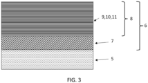
- Figure 3 shows a schematic view of a cross section of an embodiment of the coated cutting tool of the present invention having a substrate 5 and a coating 6.
- the coating 6 consisting of a first (Ti,AI)N innermost layer 7 followed by a nano-multilayer 8 of alternating nanolayers 9, 10 and 11 being Ti 1-x Al x N, Ti 1-y Si y N, and Ti 1-z Al z N.
- the nano-multilayer 8 suitably comprises a repeating sequence of consecutive nanolayers of the first nanolayer type 9, Ti 1-x Al x N, the second nanolayer type 10, Ti 1-y Si y N, and the third nanolayer type 11, Ti 1-z Al z N, in the order Ti 1-x Al x N/ Ti 1-z Al z N/ Ti 1-x Al x N/ Ti 1-y Si y N.
- the nano-multilayer 8 suitably comprises a repeating sequence of consecutive nanolayers of the first nanolayer type 9, Ti 1-x Al x N, the second nanolayer type 10, Ti 1-y Si y N, and the third nanolayer type 11, Ti 1-z Al z N, in the order Ti 1-x Al x N/ Ti 1-y Si y N/ Ti 1-z Al z N/ Ti 1-y Si y N.
- the nano-multilayer 8 suitably comprises a repeating sequence of consecutive nanolayers of the first nanolayer type 9, Ti 1-x Al x N, the second nanolayer type 10, Ti 1-y Si y N, and the third nanolayer type 11, Ti 1-z Al z N, in the order Ti 1-z Al z N/ Ti 1-x Al x N/ Ti 1-z Al z N / Ti 1-y Si y N.
- the nano-multilayer 8 suitably comprises a repeating sequence of consecutive nanolayers of the first nanolayer type 9, Ti 1-x Al x N, the second nanolayer type 10, Ti 1-y Si y N, and the third nanolayer type 11, Ti 1-z Al z N, in the order Ti 1-x Al x N/ Ti 1-y Si y N/ Ti 1-z Al z N.
- the coating 6 comprises an inner layer 7, preferably closest to the substrate 5, of (Ti,AI)N below the nano-multilayer 8 wherein the inner layer 7 is a (Ti,AI)N layer being a (Ti,AI)N nano-multilayer of alternating nanolayers of Ti 1-u Al u N, 0.35 ⁇ u ⁇ 0.67, suitably 0.40 ⁇ u ⁇ 0.67, preferably 0.45 ⁇ u ⁇ 0.62 and Ti 1-v Al v N, 0.70 ⁇ v ⁇ 0.90, suitably 0.70 ⁇ v ⁇ 0.80.
- the average nanolayer thickness of the Ti 1-u Al u N layers in the (Ti,AI)N nano-multilayer is suitably from 1 to 30 nm, preferably from 1 to 20 nm, most preferably from 2 to 10 nm.
- the thickness of this inner layer 7 is suitably from about 0.1 to about 3 ⁇ m, preferably from about 0.5 to about 2 ⁇ m.
- Coated cutting tools comprising a nano-multilayer of Ti 0.85 Si 0.15 N, Ti 0.50 Al 0.50 N and Ti 0.20 Al 0.80 N nanolayers deposited on sintered cemented carbide cutting tool insert blanks of the geometries CNMG120408MM and R390-11T308M-PM.
- the composition of the cemented carbide was 10 wt% Co, 0.4 wt% Cr and rest WC.
- the cemented carbide blanks were coated by cathodic arc evaporation in a vacuum chamber comprising four arc flanges, each flange comprising several cathode evaporators.
- Targets of Ti 0.50 Al 0.50 were mounted in the evaporators in two of the flanges opposite each other.
- the remaining targets Ti 0.85 Si 0.15 and Ti 0.20 Al 0.80 were mounted in the evaporators in the two remaining flanges opposite each other.
- the targets were circular and planar with a diameter of 100 mm available on the open market.
- Suitable target technology packages for arc evaporation are available from suppliers on the market such as IHI Hauzer Techno Coating B.V., Kobelco (Kobe Steel Ltd.) and Oerlikon Balzers.
- the uncoated blanks were mounted on pins that undergo a three-fold rotation in the PVD chamber.
- the chamber was pumped down to high vacuum (less than 10 -2 Pa) and heated to about 450-550°C by heaters located inside the chamber.
- the blanks were then etched for 60 minutes in an Ar plasma.
- an innermost layer of Ti 0.50 Al 0.50 N was deposited by only using the Ti 0.50 Al 0.50 targets.
- the chamber pressure (reaction pressure) was set to 4 Pa of N 2 gas, and a DC bias voltage of -50 V (relative to the chamber walls) was applied to the blank assembly.
- the cathodes were run in an arc discharge mode at a current of 150 A (each) for 70 minutes (2 flanges).
- the table rotational speed was 5 rpm.
- a layer of Ti 0.50 Al 0.50 N having a thickness of about 1.4 ⁇ m was deposited on the blanks.
- the nano-multilayer was deposited by using all mounted targets.
- the chamber pressure (reaction pressure) was set to 4 Pa of N 2 gas, and a DC bias voltage of -70 V (relative to the chamber walls) was applied to the blank assembly.
- the cathodes were run in an arc discharge mode at a current of 150 A (each) for 35 minutes (4 flanges).
- the table rotational speed was 5 rpm.
- a nano-multilayer coating having a thickness of about 1.4 ⁇ m was deposited on the blanks.
- the rotational speed correlates to a certain period thickness and it was concluded that a table rotational speed of 5 rpm for the current deposition rate and equipment used correlates to an average individual nanolayer thickness of each of the nanolayers Ti 0.50 Al 0.50 N, Ti 0.85 Si 0.15 N and Ti 0.20 Al 0.80 N of about 2 nm.
- the number of nanolayers in the nano-multilayer is about 700.
- the nano-multilayer comprises a repeating sequence of consecutive nanolayers in the order Ti 0.50 Al 0.50 N/ Ti 0.20 Al 0.80 N/ Ti 0.50 Al 0.50 N/ Ti 0.85 Si 0.15 N.
- an outermost layer of Ti 0.85 Si 0.15 N in order to obtain an even colour between the individual coated cutting tools made, was deposited by only using the Ti 0.85 Si 0.15 target. All deposition parameters were the same as for depositing the previous layer, except for the bias being -60 V and the cathodes were run for 10 minutes (1 flange). A layer of Ti 0.85 Si 0.15 N was deposited to a thickness of about 0.2 ⁇ m.
- the ratio is estimated from a deposition rate from each target assumed to be the same, the rotation during deposition and the deposition time.
- the coated cutting tools were called "Sample 1 (invention)”.
- Coated cutting tools comprising a nano-multilayer of Ti 0.85 Si 0.15 N, and Ti 0.20 Al 0.80 N nanolayers deposited on sintered cemented carbide cutting tool insert blanks of the geometries CNMG120408MM and R390-11T308M-PM.
- the composition of the cemented carbide was 10 wt% Co, 0.4 wt% Cr and rest WC.
- the cemented carbide blanks were coated by cathodic arc evaporation in a vacuum chamber comprising four arc flanges, each flange comprising several cathode evaporators.
- Targets of Ti 0.50 Al 0.50 were mounted in the evaporators in two of the flanges opposite each other.
- the remaining targets Ti 0.85 Si 0.15 and Ti 0.20 Al 0.80 were mounted in the evaporators in the two remaining flanges opposite each other.
- the targets were circular and planar with a diameter of 100 mm available on the open market.
- Suitable target technology packages for arc evaporation are available from suppliers on the market such as IHI Hauzer Techno Coating B.V., Kobelco (Kobe Steel Ltd.) and Oerlikon Balzers.
- the uncoated blanks were mounted on pins that undergo a three-fold rotation in the PVD chamber.
- the chamber was pumped down to high vacuum (less than 10 -2 Pa) and heated to about 450-550°C by heaters located inside the chamber.
- the blanks were then etched for 60 minutes in an Ar plasma.
- the chamber pressure (reaction pressure) was set to 4 Pa of N 2 gas, and a DC bias voltage of -50 V (relative to the chamber walls) was applied to the blank assembly.
- the cathodes were run in an arc discharge mode at a current of 150 A (each) for 70 minutes (2 flanges).
- the table rotational speed was 5 rpm.
- a layer of having a thickness of about 1.4 ⁇ m was deposited on the blanks.
- the nano-multilayer was deposited by alternating the use of the Ti 0.85 Si 0.15 and Ti 0.20 Al 0.80 targets, creating a first sequence of a Ti 0.85 Si 0.15 N/ Ti 0.20 Al 0.80 N nano-multilayer of about 35 nm thickness.
- the table rotational speed was 5 rpm.
- the Ti 0.50 Al 0.50 targets were used creating a Ti 0.50 Al 0.50 N layer of about 35 nm thickness. This procedure was repeated until 20 sequences of a nano-multilayer sequence of nanolayers Ti 0.85 Si 0.15 N and Ti 0.20 Al 0.80 N combined with a "monolayer" of Ti 0.50 Al 0.50 N was completed.
- the total thickness of the deposited nano-multilayer was about 1.4 ⁇ m.
- the chamber pressure (reaction pressure) was set to 4 Pa of N 2 gas, and a DC bias voltage of -40 V (relative to the chamber walls) was applied to the blank assembly when using the Ti 0.85 Si 0.15 and Ti 0.20 Al 0.80 targets and a DC bias voltage of -80 V (relative to the chamber walls) when using the Ti 0.50 Al 0.50 targets.
- the cathodes were run in an arc discharge mode at a current of 150 A (each) for 70 minutes (2 flanges at a time).
- the table rotational speed was 5 rpm.
- a nano-multilayer coating having a thickness of about 1.4 ⁇ m was deposited on the blanks.
- the rotational speed correlates to a certain period thickness and it was concluded that a table rotational speed of 5 rpm for the current deposition rate and equipment used correlates to an average individual nanolayer thickness of each of the nanolayers Ti 0.85 Si 0.15 N and Ti 0.20 Al 0.80 N of about 2 nm.
- an outermost layer of Ti 0.85 Si 0.15 N in order to obtain an even colour between the individual coated cutting tools made, was deposited by only using the Ti 0.85 Si 0.15 target. All deposition parameters were the same as for depositing the previous layer, except for the bias being -60 V and the cathodes were run for 10 minutes (1 flange). A layer of Ti 0.85 Si 0.15 N was deposited to a thickness of about 0.2 ⁇ m.
- the coated cutting tools were called “Sample 2 (comparative)”.
- Three different sets of samples of coated cutting tools were provided comprising a nano-multilayer of Ti 0.80 Si 0.20 N, T 0.40 Al 0.60 N nanolayers and, respectively, one of a high-AI Ti 0.25 Al 0.75 N, Ti 0.15 Al 0.85 N or Ti 0.05 Al 0.95 N nanolayers deposited on sintered cemented carbide cutting tool insert blanks of the geometries CNMG120408MM and R390-11T308M-PM.
- the composition of the cemented carbide was 10 wt% Co, 0.4 wt% Cr and rest WC.
- the cemented carbide blanks were coated by cathodic arc evaporation in a vacuum chamber comprising four arc flanges, each flange comprising several cathode evaporators.
- Targets of Ti 0.80 Si 0.20 were mounted in the evaporators in two of the flanges opposite each other.
- the remaining targets Ti 0.40 Al 0.60 and the high-AI (Ti,AI) target used (Ti 0.25 Al 0.75 , Ti 0.15 Al 0.85 or T 0.05 Al 0.95 , respectively, in the three differents runs) were mounted in the evaporators in the two remaining flanges opposite each other.
- the targets were circular and planar with a diameter of 100 mm available on the open market. Suitable target technology packages for arc evaporation are available from suppliers on the market such as IHI Hauzer Techno Coating B.V., Kobelco (Kobe Steel Ltd.) and Oerlikon Balzers.
- the uncoated blanks were mounted on pins that undergo a three-fold rotation in the PVD chamber.
- the chamber was pumped down to high vacuum (less than 10 -2 Pa) and heated to about 450-550°C by heaters located inside the chamber.
- the blanks were then etched for 60 minutes in an Ar plasma.
- an innermost layer of Ti 0.40 Al 0.60 N was deposited by only using the Ti 0.40 Al 0.60 target.
- the chamber pressure (reaction pressure) was set to 4 Pa of N 2 gas, and a DC bias voltage of -70 V (relative to the chamber walls) was applied to the blank assembly.
- the cathodes were run in an arc discharge mode at a current of 150 A (each) for 100 minutes (1 flange).
- the table rotational speed was 5 rpm.
- a layer of Ti 0.40 Al 0.60 N having a thickness of about 1 ⁇ m was deposited on the blanks.
- the nano-multilayer was deposited by using all mounted targets.
- the chamber pressure (reaction pressure) was set to 4 Pa of N 2 gas, and a DC bias voltage of -100 V (relative to the chamber walls) was applied to the blank assembly.
- the cathodes were run in an arc discharge mode at a current of 150 A (each) for 50 minutes (4 flanges).
- the table rotational speed was 5 rpm.
- a nano-multilayer coating having a thickness of about 2 ⁇ m was deposited on the blanks.
- a table rotational speed of 5 rpm for the current deposition rate and equipment used correlates to an average individual nanolayer thickness of each of the nanolayers Ti 0.40 Al 0.60 N, Ti 0.80 Si 0.20 N and also Ti 0.25 Al 0.75 N, Ti 0.15 Al 0.85 N and Ti 0.05 Al 0.95 N, respectively, in the three different nano-multilayers made of about 2 nm.
- the number of nanolayers in all three different sets of nano-multilayers is about 1000.
- the nano-multilayer of the first set of samples comprises a repeating sequence of consecutive nanolayers in the order Ti 0.40 Al 0.60 N/ Ti 0.80 Si 0.20 N/ Ti 0.25 Al 0.75 N/ Ti 0.80 Si 0.20 N.
- the nano-multilayer of the second set of samples comprises a repeating sequence of consecutive nanolayers in the order Ti 0.40 Al 0.60 N/ Ti 0.80 Si 0.20 N/ Ti 0.15 Al 0.85 N/ Ti 0.80 Si 0.20 N.
- the nano-multilayer of the third set of samples comprises a repeating sequence of consecutive nanolayers in the order Ti 0.40 Al 0.60 N/ Ti 0.80 Si 0.20 N/ Ti 0.05 Al 0.95 N/ Ti 0.80 Si 0.20 N.
- an outermost layer in order to obtain an even colour between the individual coated cutting tools made, was deposited by only using the respective high-Al (Ti,AI) target used when depositing the respective nano-multilayer for the three different sets of samples. All deposition parameters were the same as for depositing the previous layer, except for the bias being -100 V and the cathodes were run for 10 minutes (1 flange).
- a layer of Ti 0.25 Al 0.75 N, Ti 0.15 Al 0.85 N or Ti 0.05 Al 0.95 N was deposited, respectively, on the three different sets of samples, to a thickness of about 0.2 ⁇ m.
- the ratio is estimated from a deposition rate from each target assumed to be the same, the rotation during deposition and the deposition time.
- the coated cutting tools made were called:
- Coated cutting tools comprising a nano-multilayer of Ti 0.80 Si 0.20 N, T 0.40 Al 0.60 N and Ti 0.25 Al 0.75 N nanolayers deposited on sintered cemented carbide cutting tool insert blanks of the geometries CNMG120408MM and R390-11T308M-PM.
- the composition of the cemented carbide was 10 wt% Co, 0.4 wt% Cr and rest WC.
- the cemented carbide blanks were coated by cathodic arc evaporation in a vacuum chamber comprising four arc flanges, each flange comprising several cathode evaporators.
- Targets of Ti 0.80 Si 0.20 were mounted in the evaporators in two of the flanges opposite each other.
- the remaining targets Ti 0.40 Al 0.60 and Ti 0.25 Al 0.75 were mounted in the evaporators in the two remaining flanges opposite each other.
- the targets were circular and planar with a diameter of 100 mm available on the open market.
- Suitable target technology packages for arc evaporation are available from suppliers on the market such as IHI Hauzer Techno Coating B.V., Kobelco (Kobe Steel Ltd.) and Oerlikon Balzers.
- the uncoated blanks were mounted on pins that undergo a three-fold rotation in the PVD chamber.
- the chamber was pumped down to high vacuum (less than 10 -2 Pa) and heated to about 450-550°C by heaters located inside the chamber.
- the blanks were then etched for 60 minutes in an Ar plasma.
- an innermost layer being a nano-multilayer of Ti 0.40 Al 0.60 N and Ti 0.25 Al 0.75 N nanolayers was deposited by only using the Ti 0.40 Al 0.60 and Ti 0.25 Al 0.75 targets.
- the chamber pressure (reaction pressure) was set to 4 Pa of N 2 gas, and a DC bias voltage of -100 V (relative to the chamber walls) was applied to the blank assembly.
- the cathodes were run in an arc discharge mode at a current of 150 A (each) for 50 minutes (2 flanges).
- the table rotational speed was 5 rpm.
- a layer of a nano-multilayer of Ti 0.40 Al 0.60 N and Ti 0.25 Al 0.75 N having a thickness of about 1 ⁇ m was deposited on the blanks. Since the rotational speed for the current deposition rate and equipment used correlates to a certain period thickness it was concluded that the average individual nanolayer thickness was about 2 nm.
- the nano-multilayer of Ti 0.80 Si 0.20 N, Ti 0.40 Al 0.60 N and Ti 0.25 Al 0.75 N nanolayers was deposited by using all mounted targets.
- the chamber pressure (reaction pressure) was set to 4 Pa of N 2 gas, and a DC bias voltage of -100 V (relative to the chamber walls) was applied to the blank assembly.
- the cathodes were run in an arc discharge mode at a current of 150 A (each) for 50 minutes (4 flanges).
- the table rotational speed was 5 rpm.
- a nano-multilayer coating having a thickness of about 2 ⁇ m was deposited on the blanks.
- the rotational speed correlates to a certain period thickness and it was concluded that a table rotational speed of 5 rpm for the current deposition rate and equipment used correlates to an average individual nanolayer thickness of each of the nanolayers Ti 0.40 Al 0.60 N, Ti 0.80 Si 0.20 N and Ti 0.25 Al 0.75 N of about 2 nm.
- the number of nanolayers in the nano-multilayer is about 1000.
- the nano-multilayer comprises a repeating sequence of consecutive nanolayers in the order Ti 0.40 Al 0.60 N/ Ti 0.80 Si 0.20 N / Ti 0.25 Al 0.75 N/ Ti 0.80 Si 0.20 N.
- an outermost layer of Ti 0.25 Al 0.75 N in order to obtain an even colour between the individual coated cutting tools made, was deposited by only using the Ti 0.25 Al 0.75 target. All deposition parameters were the same as for depositing the previous layer, and the cathodes were run for 10 minutes (1 flange). A layer of Ti 0.25 Al 0.75 N was deposited to a thickness of about 0.2 ⁇ m.
- the ratio is estimated from a deposition rate from each target assumed to be the same, the rotation during deposition and the deposition time.
- the coated cutting tools were called "Sample 6".
- Coated cutting tools comprising a nano-multilayer of Ti 0.80 Si 0.20 N, T 0.40 Al 0.60 N and Ti 0.15 Al 0.85 N nanolayers deposited on sintered cemented carbide cutting tool insert blanks of the geometries CNMG120408MM and R390-11T308M-PM.
- the composition of the cemented carbide was 10 wt% Co, 0.4 wt% Cr and rest WC.
- the cemented carbide blanks were coated by cathodic arc evaporation in a vacuum chamber comprising four arc flanges, each flange comprising several cathode evaporators. Two targets of Ti 0.15 Al 0.85 were mounted in the evaporators in two of the flanges opposite each other.
- the remaining targets Ti 0.40 Al 0.60 and Ti 0.80 Si 0.20 were mounted in the evaporators in the two remaining flanges opposite each other.
- the targets were circular and planar with a diameter of 100 mm available on the open market.
- Suitable target technology packages for arc evaporation are available from suppliers on the market such as IHI Hauzer Techno Coating B.V., Kobelco (Kobe Steel Ltd.) and Oerlikon Balzers.
- the uncoated blanks were mounted on pins that undergo a three-fold rotation in the PVD chamber.
- the chamber was pumped down to high vacuum (less than 10 -2 Pa) and heated to about 450-550°C by heaters located inside the chamber.
- the blanks were then etched for 60 minutes in an Ar plasma.
- an innermost layer of Ti 0.40 Al 0.60 N was deposited by only using the Ti 0.40 Al 0.60 target.
- the chamber pressure (reaction pressure) was set to 4 Pa of N 2 gas, and a DC bias voltage of -70 V (relative to the chamber walls) was applied to the blank assembly.
- the cathodes were run in an arc discharge mode at a current of 150 A (each) for 100 minutes (1 flange).
- the table rotational speed was 5 rpm.
- a layer of Ti 0.40 Al 0.60 N having a thickness of about 1 ⁇ m was deposited on the blanks.
- the nano-multilayer was deposited by using all mounted targets.
- the chamber pressure (reaction pressure) was set to 4 Pa of N 2 gas, and a DC bias voltage of -100 V (relative to the chamber walls) was applied to the blank assembly.
- the cathodes were run in an arc discharge mode at a current of 150 A (each) for 50 minutes (4 flanges).
- the table rotational speed was 5 rpm.
- a nano-multilayer coating having a thickness of about 2 ⁇ m was deposited on the blanks.
- the rotational speed correlates to a certain period thickness and it was concluded that a table rotational speed of 5 rpm for the current deposition rate and equipment used correlates to an average individual nanolayer thickness of each of the nanolayers Ti 0.40 Al 0.60 N, Ti 0.80 Si 0.20 N and Ti 0.15 Al 0.85 N of about 2 nm.
- the number of nanolayers in the nano-multilayer is about 1000.
- the nano-multilayer comprises a repeating sequence of consecutive nanolayers in the order Ti 0.15 Al 0.85 N/ Ti 0.40 Al 0.60 N/ Ti 0.15 Al 0.85 N/ Ti 0.80 Si 0.20 N.
- an outermost layer of Ti 0.15 Al 0.85 N in order to obtain an even colour between the individual coated cutting tools made, was deposited by only using the Ti 0.15 Al 0.85 target. All deposition parameters were the same as for depositing the previous layer and the cathodes were run for 10 minutes (1 flange). A layer of Ti 0.15 Al 0.85 N was deposited to a thickness of about 0.2 ⁇ m.
- the coated cutting tools were called "Sample 7".
- the ratio is estimated from a deposition rate from each target assumed to be the same, the rotation during deposition and the deposition time.
- z (number) number of teeth in the cutter
- the cut-off criteria for tool life is a flank wear VB of 0.15 mm.
- the evaluation was made through turning test in austenitic stainless steel. In order to provoke adhesive wear and flaking of the coating the depth of cut a p was varied between 4 to 0 and 0 to 4 mm (in one run during radial facing). The inserts were evaluated through SEM analysis.
- samples 1, 3, 4, 6 and 7, within the invention have high flank wear resistance and show much less flank wear than comparative samples 2 and 5 outside the invention.
- Sample 3 and sample 6 differ in that sample 6 has an inner (Ti,AI)N nano-multilayer instead of a single (Ti,AI)N layer. Further cutting tests were made on Sample 3 and Sample 6 in order to determine the effect on comb crack resistance and edge line toughness by having the alternative inner layer in Sample 6.
- the criteria for end of tool life is a max. chipped height VB>0.3 mm.
- the cut-off criteria are chipping of at least 0.5 mm of the edge line or a measured depth of 0.2 mm at either the flank- or the rake phase. Tool life is presented as the number of cut entrances in order to achieve these criteria. Table 5.
- Edge line toughness (No. cuts) 3 invention Ti 0.40 Al 0.60 N, Ti 0.40 Al 0.60 N/ Ti 0.80 Si 0.20 N/ Ti 0.25 Al 0.75 N 29 24 6 invention nano-multi Ti 0.40 Al 0.60 N/ Ti 0.25 Al 0.75 N Ti 0.40 Al 0.60 N/ Ti 0.80 Si 0.20 N/ Ti 0.25 Al 0.75 N 37 50
Landscapes
- Chemical & Material Sciences (AREA)
- Engineering & Computer Science (AREA)
- Mechanical Engineering (AREA)
- Materials Engineering (AREA)
- Metallurgy (AREA)
- Organic Chemistry (AREA)
- Chemical Kinetics & Catalysis (AREA)
- Inorganic Chemistry (AREA)
- Cutting Tools, Boring Holders, And Turrets (AREA)
- Physical Vapour Deposition (AREA)
- Milling Processes (AREA)
- Drilling Tools (AREA)
Abstract
Description
- The present invention relates to a coated cutting tool comprising a coating comprising a nano-multilayer of alternating nanolayers of Ti1-xAlxN, 0.35≤x<0.67, Ti1-ySiyN, 0.10≤y≤0.25, and Ti1-zAlzN, 0.70≤y≤0.90.
- Metal machining operations include, for example, turning, milling, and drilling. In order to provide a long tool life, a coated cutting tool, such as an insert, should have high resistance against different types of wear. In order to increase wear resistance of a cutting tool various types of wear resistant coatings are known in the art.
- A cutting tool generally has at least one rake face and at least one flank face. A cutting edge is present where a rake face and flank face meet.
- Flank wear obviously takes place on a flank face of the cutting edge, mainly from an abrasive wear mechanism. The flank face is subjected to workpiece movement and too much flank wear will lead to poor surface texture of the workpiece, inaccuracy in the cutting process and increased friction in the cutting process.
- If a better flank wear resistance is provided longer tool life is provided for certain metal machining operations.
- A coating must also remain adherent to the substrate, i.e., not flake off, during a machining operation. Some workpiece material types such as ISO-M (stainless steel) and ISO-S (heat resistant super alloys and, e.g., titanium), are so called sticky materials and induce flaking more than other workpiece material types. These material types also have a smearing behaviour which means that workpiece material is smeared onto the cutting tool surface which eventually may lead to the formation of a built-up edge (BUE) of workpiece material on the cutting edge. Such a BUE may cause the coating to flake off or even rip off a part of the edge of the cutting tool.
- Different metal machining operations affect a coated cutting tool in different ways. Turning, for example, is a continuous metal machining operation while milling is more intermittent in nature. In milling the thermal and mechanical load will vary over time. Thermal load induces thermal tensions which may lead to so-called thermal cracks, herein referred to as "comb cracks", in the coatings, while the later may cause fatigue in the cutting edge leading to chipping, i.e., small fragments of the cutting edge loosening from the rest of the substrate. Thus, common wear types of a coated cutting tool in milling are cracking and chipping. A high level of toughness of the coating, in particular at the cutting edge, may reduce such chipping. A high comb crack resistance and edge line toughness are thus of great importance for tool lifetime.
- There is a continuing demand for coated cutting tools in which the coating has excellent properties in terms of wear resistance, edge line toughness, comb crack resistance, flaking resistance, etc. in order to provide a cutting tool with superior properties than currently available cutting tools on the market. If one or more of the above-mentioned properties are improved then longer tool life is provided.
- Nano-multilayered coatings are being used in the area of cutting tools for metal machining. In these coatings at least two layers which are different in some respect alternate forming a coating of a stack of nanolayers.
- There is an object of the present invention to provide a coated cutting tool which, at least, shows high flank wear resistance and high flaking resistance.
- The object of the invention is provided by a coated cutting tool comprising a substrate and a coating, wherein the coating comprises a from about 0.5 to about 10 µm nano-multilayer of alternating nanolayers of a first nanolayer type being Ti1-xAlxN, 0.35≤x<0.67, a second nanolayer type being Ti1-ySiyN, 0.10≤y≤0.25, and a third nanolayer type being Ti1-zAlzN, 0.70≤z≤0.90, the average nanolayer thickness of each of the nanolayer types Ti1-xAlxN, Ti1-ySiyN, and Ti1-zAlzN in the nano-multilayer is from 1 to 30 nm.
- By "nano-multilayer of alternating nanolayers of a first nanolayer type, a second nanolayer type, and a third nanolayer type" is herein meant that the different types of nanolayers are generally alternating in a certain order in the nano-multilayer. However, due to the way chosen for depositing the nano-multilayer in a PVD reactor, for example using a so called three-fold rotation of the tools being coated, there may be an altering of the order of the three types of nanolayers at some places within the nano-multilayer.
- In one embodiment there is a ratio in the nano-multilayer between the sum of nanolayer thicknesses of all of each nanolayer types, Ti1-xAlxN:Ti1-ySiyN:Ti1-zAlzN, being a:b:c, wherein 0.5<a<3, 0.5<b<3, 0.5<c<3, preferably 0.75<a<2.5, 0.75<b<2.5, 0.75<c<2.5, most preferably 0.9<a<2.25, 0.9<b<2.25, 0.9<c<2.25.
- The ratio between the sum of nanolayer thicknesses of each nanolayer type, Ti1-xAlxN:Ti1-ySiyN:Ti1-zAlzN, in the nano-multilayer, i.e., a:b:c, can be determined by Scanning Transmission Electron Microscopy (STEM) analysis, preferably in combination with Energy-dispersive X-ray spectroscopy (EDS), where over a distance along a normal to the substrate surface the elemental composition and thicknesses of individual nanolayers are determined. A distance of at least 25 times the average nanolayer thickness is used. The sum of nanolayer thicknesses for nanolayers of the first nanolayer type Ti1-xAlxN is "a", The sum of nanolayer thicknesses for nanolayers of the first nanolayer type Ti1-xAlxN is "a", the sum of nanolayer thicknesses for nanolayers of the second nanolayer type Ti1-ySiyN is "b", and the sum of nanolayer thicknesses for nanolayers of the third nanolayer type Ti1-zAlzN is "c".
- The average nanolayer thickness of each of the nanolayer types Ti1-xAlxN, Ti1-ySiyN, and Ti1-zAlzN in the nano-multilayer can also be determined by the above described STEM/EDS analysis.
- For the first nanolayer type being Ti1-xAlxN, suitably 0.40≤x≤0.67, preferably 0.45≤x≤0.62.
- For the second nanolayer type being Ti1-ySiyN, suitably 0.13≤y≤0.23, preferably 0.17≤y≤0.21.
- For the third nanolayer type being Ti1-zAlzN, suitably 0.70<z≤0.85, preferably 0.75<z≤0.85.
- The average nanolayer thickness in the nano-multilayer of each of the nanolayer types Ti1-xAlxN, Ti1-ySiyN, and Ti1-zAlzN in the nano-multilayer is suitably from 1 to 20 nm, preferably from 1.5 to 10 nm, most preferably from 2 to 5 nm.
- The ratio of average nanolayer thickness in the nano-multilayer between any one of the nanolayer types Ti1-xAlxN, Ti1-ySiyN, and Ti1-zAlzN to any of the remaining two of the nanolayer types Ti1-xAlxN, Ti1-ySiyN, and Ti1-zAlzN in the nano-multilayer is suitably of from 0.1 to 10, preferably from 0.5 to 5, most preferably from 0.8 to 2.
- Suitably, within a sequence of 10 consecutive nanolayers, preferably 8, most preferably 6, consecutive nanolayers, in the nano-multilayer there are all of the nanolayer types Ti1-xAlxN, Ti1-ySiyN, and Ti1-zAlzN present.
- The thickness of the nano-multilayer is suitably from about 1 to about 8 µm, preferably from about 1.5 to about 5 µm.
- In one embodiment, the coating comprises an inner layer of TiN or (Ti,AI)N below the nano-multilayer, preferably closest to the substrate. The (Ti,AI)N layer may either be a monolayer or a nano-multilayer of alternating nanolayers of different Ti/AI ratio. Preferably, the inner layer is (Ti,AI)N. If (Ti,AI)N is used as the inner layer then the (Ti,AI)N is suitably Ti1-tAltN, 0.35≤t≤0.67, preferably 0.40≤t≤0.67, most preferably 0.45≤t≤0.62. In a preferred embodiment the Ti-AI relation in the (Ti,AI)N of the inner layer is the same as the Ti-AI relation in the first nanolayer type of the nano-multilayer. This is because this simplifies the production when a same target can be used as already being used for the nano-multilayer. The thickness of this inner layer is suitably from about 0.1 to about 3 µm, preferably from about 0.5 to about 2 µm.
- In one embodiment, for the purpose of having control of the colour of the coated cutting tool, the coating comprises an outermost single layer of any one of the first nanolayer type Ti1-xAlxN, 0.35≤x<0.67, the second nanolayer type Ti1-ySiyN, 0.10≤y≤0.25, or the third nanolayer type Ti1-zAlzN, 0.70≤z≤0.90.
- The values of x, y or z in the outermost layer is preferably the same as x, y or z in the Ti1-xAlxN, Ti1-ySiyN, or Ti1-zAlzN in the nano-multilayer. This is because this simplifies the production when a same target can be used as already being used for the nano-multilayer.
- The thickness of this outermost layer is suitably from about 0.1 to about 0.5 µm, preferably from about 0.1 to about 0.3 µm.
- The nanolayers of the first nanolayer type, the second nanolayer type and the third nanolayer type are suitably cathodic arc evaporation deposited layers. Also the optional inner layer of TiN or (Ti,AI)N, as well as the optional outermost single layer are suitably cathodic arc evaporation deposited layers.
- The substrate of the coated cutting tool can be selected from the group of cemented carbide, cermet, ceramic, cubic boron nitride and high speed steel. In one embodiment the substrate is a cemented carbide comprising from 5 to 18 wt% Co
- The coated cutting tool is suitably a cutting tool insert, a drill, or a solid end-mill, for metal machining. The cutting tool insert is, for example, a turning insert or a milling insert.
-
-
Figure 1 shows a schematic view of one embodiment of a cutting tool being a milling insert. -
Figure 2 shows a schematic view of one embodiment of a cutting tool being a turning insert. -
Figure 3 shows a schematic view of a cross section of an embodiment of the coated cutting tool of the present invention showing a substrate and a coating comprising different layers. -
Figure 1 shows a schematic view of one embodiment of a cutting tool (1) having arake face 2 and flank faces 3 and acutting edge 4. The cutting tool 1 is in this embodiment a milling insert.Figure 2 shows a schematic view of one embodiment of a cutting tool 1 having arake face 2 andflank face 3 and acutting edge 4. The cutting tool 1 is in this embodiment a turning insert.Figure 3 shows a schematic view of a cross section of an embodiment of the coated cutting tool of the present invention having asubstrate 5 and acoating 6. Thecoating 6 consisting of a first (Ti,AI)Ninnermost layer 7 followed by a nano-multilayer 8 of alternating nanolayers 9, 10 and 11 being Ti1-xAlxN, Ti1-ySiyN, and Ti1-zAlzN. - In one embodiment, there is a ratio in the nano-
multilayer 8 between the sum of nanolayer thicknesses of each nanolayer type 9, 10, 11, Ti1-xAlxN:Ti1-ySiyN:Ti1-zAlzN,in the nano-multilayer 8, a:b:c, 1.5<a<2.5, 0.75<b<1.25, 0.75<c<1.25, preferably 1.75<a<2.25, 0.9<b<1.1, 0.9<c<1.1. In this embodiment the nano-multilayer 8 suitably comprises a repeating sequence of consecutive nanolayers of the first nanolayer type 9, Ti1-xAlxN, the second nanolayer type 10, Ti1-ySiyN, and the third nanolayer type 11, Ti1-zAlzN, in the order Ti1-xAlxN/ Ti1-zAlzN/ Ti1-xAlxN/ Ti1-ySiyN. The nano-multilayer 8 is suitably composed of (Ti1-xAlxN/ Ti1-zAlzN/ Ti1-xAlxN/ Ti1-ySiyN..)m, m=15-1500, suitably m=30-800. - In a further embodiment, there is a ratio in the nano-
multilayer 8 between the sum of nanolayer thicknesses of each nanolayer type 9, 10, 11, Ti1-xAlxN:Ti1-ySiyN:Ti1-zAlzN, in the nano-multilayer 8, a:b:c, 0.75<a<1.25, 1.5<b<2.5, 0.75<c<1.25, preferably 0.9<a<1.1, 1.75<b<2.25, 0.9<c<1.1. In this embodiment the nano-multilayer 8 suitably comprises a repeating sequence of consecutive nanolayers of the first nanolayer type 9, Ti1-xAlxN, the second nanolayer type 10, Ti1-ySiyN, and the third nanolayer type 11, Ti1-zAlzN, in the order Ti1-xAlxN/ Ti1-ySiyN/ Ti1-zAlzN/ Ti1-ySiyN. The nano-multilayer (8) is suitably composed of (Ti1-xAlxN/ Ti1-ySiyN/ Ti1-zAlzN/ Ti1-ySiyN)n, n=15-1500, suitably n=30-800. - In a further embodiment, there is a ratio in the nano-
multilayer 8 between the sum of nanolayer thicknesses of each nanolayer type 9, 10, 11, Ti1-xAlxN:Ti1-ySiyN:Ti1-zAlzN, in the nano-multilayer 8, a:b:c, 0.75<a<1.25, 0.75<b<1.25, 1.5<c<2.5, preferably 0.9<a<1.1, 0.9<b<1.1, 1.75<c<2.25. In this embodiment the nano-multilayer 8 suitably comprises a repeating sequence of consecutive nanolayers of the first nanolayer type 9, Ti1-xAlxN, the second nanolayer type 10, Ti1-ySiyN, and the third nanolayer type 11, Ti1-zAlzN, in the order Ti1-zAlzN/ Ti1-xAlxN/ Ti1-zAlzN / Ti1-ySiyN. The nano-multilayer 8 is suitably composed of (Ti1-zAlzN/ Ti1-xAlxN/ Ti1-zAlzN / Ti1-ySiyN)p, p=15-1500, suitably p=30-800. - In a further embodiment, there is a ratio in the nano-
multilayer 8 between the sum of nanolayer thicknesses of each nanolayer type 9, 10, 11, Ti1-xAlxN:Ti1-ySiyN:Ti1-zAlzN, in the nano-multilayer 8, a:b:c, 0.75<a<1.25, 0.75<b<1.25, 0.75<c<1.25, preferably 0.9<a<1.1, 0.9<b<1.1, 0.9<c<1.1. In this embodiment the nano-multilayer 8 suitably comprises a repeating sequence of consecutive nanolayers of the first nanolayer type 9, Ti1-xAlxN, the second nanolayer type 10, Ti1-ySiyN, and the third nanolayer type 11, Ti1-zAlzN, in the order Ti1-xAlxN/ Ti1-ySiyN/ Ti1-zAlzN. The nano-multilayer 8 is suitably composed of (Ti1-xAlxN/ Ti1-ySiyN/ Ti1-zAlzN)q, q=20-2000, suitably q=40-1000. - In a further embodiment, the
coating 6 comprises aninner layer 7, preferably closest to thesubstrate 5, of (Ti,AI)N below the nano-multilayer 8 wherein theinner layer 7 is a (Ti,AI)N layer being a (Ti,AI)N nano-multilayer of alternating nanolayers of Ti1-uAluN, 0.35≤u<0.67, suitably 0.40≤u≤0.67, preferably 0.45≤u≤0.62 and Ti1-vAlvN, 0.70≤v≤0.90, suitably 0.70≤v≤0.80. - The average nanolayer thickness of the Ti1-uAluN layers in the (Ti,AI)N nano-multilayer is suitably from 1 to 30 nm, preferably from 1 to 20 nm, most preferably from 2 to 10 nm. The thickness of this
inner layer 7 is suitably from about 0.1 to about 3 µm, preferably from about 0.5 to about 2 µm. - Coated cutting tools were provided comprising a nano-multilayer of Ti0.85Si0.15N, Ti0.50Al0.50N and Ti0.20Al0.80N nanolayers deposited on sintered cemented carbide cutting tool insert blanks of the geometries CNMG120408MM and R390-11T308M-PM. The composition of the cemented carbide was 10 wt% Co, 0.4 wt% Cr and rest WC. The cemented carbide blanks were coated by cathodic arc evaporation in a vacuum chamber comprising four arc flanges, each flange comprising several cathode evaporators. Targets of Ti0.50Al0.50 were mounted in the evaporators in two of the flanges opposite each other. The remaining targets Ti0.85Si0.15 and Ti0.20Al0.80 were mounted in the evaporators in the two remaining flanges opposite each other. The targets were circular and planar with a diameter of 100 mm available on the open market. Suitable target technology packages for arc evaporation are available from suppliers on the market such as IHI Hauzer Techno Coating B.V., Kobelco (Kobe Steel Ltd.) and Oerlikon Balzers.
- The uncoated blanks were mounted on pins that undergo a three-fold rotation in the PVD chamber.
- The chamber was pumped down to high vacuum (less than 10-2 Pa) and heated to about 450-550°C by heaters located inside the chamber. The blanks were then etched for 60 minutes in an Ar plasma.
- At first, an innermost layer of Ti0.50Al0.50N was deposited by only using the Ti0.50Al0.50 targets.
- The chamber pressure (reaction pressure) was set to 4 Pa of N2 gas, and a DC bias voltage of -50 V (relative to the chamber walls) was applied to the blank assembly. The cathodes were run in an arc discharge mode at a current of 150 A (each) for 70 minutes (2 flanges). The table rotational speed was 5 rpm. A layer of Ti0.50Al0.50N having a thickness of about 1.4 µm was deposited on the blanks.
- Then, the nano-multilayer was deposited by using all mounted targets.
- The chamber pressure (reaction pressure) was set to 4 Pa of N2 gas, and a DC bias voltage of -70 V (relative to the chamber walls) was applied to the blank assembly. The cathodes were run in an arc discharge mode at a current of 150 A (each) for 35 minutes (4 flanges). The table rotational speed was 5 rpm. A nano-multilayer coating having a thickness of about 1.4 µm was deposited on the blanks.
- The rotational speed correlates to a certain period thickness and it was concluded that a table rotational speed of 5 rpm for the current deposition rate and equipment used correlates to an average individual nanolayer thickness of each of the nanolayers Ti0.50Al0.50N, Ti0.85Si0.15N and Ti0.20Al0.80N of about 2 nm. The number of nanolayers in the nano-multilayer is about 700.
- The nano-multilayer comprises a repeating sequence of consecutive nanolayers in the order Ti0.50Al0.50N/ Ti0.20Al0.80N/ Ti0.50Al0.50N/ Ti0.85Si0.15N.
- Finally, an outermost layer of Ti0.85Si0.15N, in order to obtain an even colour between the individual coated cutting tools made, was deposited by only using the Ti0.85Si0.15 target. All deposition parameters were the same as for depositing the previous layer, except for the bias being -60 V and the cathodes were run for 10 minutes (1 flange). A layer of Ti0.85Si0.15N was deposited to a thickness of about 0.2 µm.
- In the nano-multilayer, the ratio of the sum of nanolayer thicknesses of each of the nanolayers Ti0.50Al0.50N, Ti0.85Si0.15N, Ti0.20Al0.80N, respectively, i.e., Ti0.50Al0.50N: Ti0.85Si0.15N: Ti0.20Al0.80N, is about 2:1:1. The ratio is estimated from a deposition rate from each target assumed to be the same, the rotation during deposition and the deposition time.
- The coated cutting tools were called "Sample 1 (invention)".
- Coated cutting tools were provided comprising a nano-multilayer of Ti0.85Si0.15N, and Ti0.20Al0.80N nanolayers deposited on sintered cemented carbide cutting tool insert blanks of the geometries CNMG120408MM and R390-11T308M-PM. The composition of the cemented carbide was 10 wt% Co, 0.4 wt% Cr and rest WC. The cemented carbide blanks were coated by cathodic arc evaporation in a vacuum chamber comprising four arc flanges, each flange comprising several cathode evaporators. Targets of Ti0.50Al0.50 were mounted in the evaporators in two of the flanges opposite each other. The remaining targets Ti0.85Si0.15 and Ti0.20Al0.80 were mounted in the evaporators in the two remaining flanges opposite each other. The targets were circular and planar with a diameter of 100 mm available on the open market. Suitable target technology packages for arc evaporation are available from suppliers on the market such as IHI Hauzer Techno Coating B.V., Kobelco (Kobe Steel Ltd.) and Oerlikon Balzers.
- The uncoated blanks were mounted on pins that undergo a three-fold rotation in the PVD chamber.
- The chamber was pumped down to high vacuum (less than 10-2 Pa) and heated to about 450-550°C by heaters located inside the chamber. The blanks were then etched for 60 minutes in an Ar plasma.
- At first, an innermost layer of was deposited by only using the Ti0.50Al0.50 targets.
- The chamber pressure (reaction pressure) was set to 4 Pa of N2 gas, and a DC bias voltage of -50 V (relative to the chamber walls) was applied to the blank assembly. The cathodes were run in an arc discharge mode at a current of 150 A (each) for 70 minutes (2 flanges). The table rotational speed was 5 rpm. A layer of having a thickness of about 1.4 µm was deposited on the blanks.
- Then, the nano-multilayer was deposited by alternating the use of the Ti0.85Si0.15 and Ti0.20Al0.80 targets, creating a first sequence of a Ti0.85Si0.15N/ Ti0.20Al0.80N nano-multilayer of about 35 nm thickness. The table rotational speed was 5 rpm. Then only the Ti0.50Al0.50 targets were used creating a Ti0.50Al0.50N layer of about 35 nm thickness. This procedure was repeated until 20 sequences of a nano-multilayer sequence of nanolayers Ti0.85Si0.15N and Ti0.20Al0.80N combined with a "monolayer" of Ti0.50Al0.50N was completed. The total thickness of the deposited nano-multilayer was about 1.4 µm.
- The chamber pressure (reaction pressure) was set to 4 Pa of N2 gas, and a DC bias voltage of -40 V (relative to the chamber walls) was applied to the blank assembly when using the Ti0.85Si0.15 and Ti0.20Al0.80 targets and a DC bias voltage of -80 V (relative to the chamber walls) when using the Ti0.50Al0.50 targets. The cathodes were run in an arc discharge mode at a current of 150 A (each) for 70 minutes (2 flanges at a time). The table rotational speed was 5 rpm. A nano-multilayer coating having a thickness of about 1.4 µm was deposited on the blanks.
- The rotational speed correlates to a certain period thickness and it was concluded that a table rotational speed of 5 rpm for the current deposition rate and equipment used correlates to an average individual nanolayer thickness of each of the nanolayers Ti0.85Si0.15N and Ti0.20Al0.80N of about 2 nm.
- Finally, an outermost layer of Ti0.85Si0.15N, in order to obtain an even colour between the individual coated cutting tools made, was deposited by only using the Ti0.85Si0.15 target. All deposition parameters were the same as for depositing the previous layer, except for the bias being -60 V and the cathodes were run for 10 minutes (1 flange). A layer of Ti0.85Si0.15N was deposited to a thickness of about 0.2 µm.
- The coated cutting tools were called "Sample 2 (comparative)".
- Three different sets of samples of coated cutting tools were provided comprising a nano-multilayer of Ti0.80Si0.20N, T0.40Al0.60N nanolayers and, respectively, one of a high-AI Ti0.25Al0.75N, Ti0.15Al0.85N or Ti0.05Al0.95N nanolayers deposited on sintered cemented carbide cutting tool insert blanks of the geometries CNMG120408MM and R390-11T308M-PM. The composition of the cemented carbide was 10 wt% Co, 0.4 wt% Cr and rest WC. The cemented carbide blanks were coated by cathodic arc evaporation in a vacuum chamber comprising four arc flanges, each flange comprising several cathode evaporators. Targets of Ti0.80Si0.20 were mounted in the evaporators in two of the flanges opposite each other. The remaining targets Ti0.40Al0.60 and the high-AI (Ti,AI) target used (Ti0.25Al0.75, Ti0.15Al0.85 or T0.05Al0.95, respectively, in the three differents runs) were mounted in the evaporators in the two remaining flanges opposite each other. The targets were circular and planar with a diameter of 100 mm available on the open market. Suitable target technology packages for arc evaporation are available from suppliers on the market such as IHI Hauzer Techno Coating B.V., Kobelco (Kobe Steel Ltd.) and Oerlikon Balzers.
- The uncoated blanks were mounted on pins that undergo a three-fold rotation in the PVD chamber.
- The chamber was pumped down to high vacuum (less than 10-2 Pa) and heated to about 450-550°C by heaters located inside the chamber. The blanks were then etched for 60 minutes in an Ar plasma.
- At first, an innermost layer of Ti0.40Al0.60N was deposited by only using the Ti0.40Al0.60 target. The chamber pressure (reaction pressure) was set to 4 Pa of N2 gas, and a DC bias voltage of -70 V (relative to the chamber walls) was applied to the blank assembly. The cathodes were run in an arc discharge mode at a current of 150 A (each) for 100 minutes (1 flange). The table rotational speed was 5 rpm. A layer of Ti0.40Al0.60N having a thickness of about 1 µm was deposited on the blanks.
- Then, the nano-multilayer was deposited by using all mounted targets.
- The chamber pressure (reaction pressure) was set to 4 Pa of N2 gas, and a DC bias voltage of -100 V (relative to the chamber walls) was applied to the blank assembly. The cathodes were run in an arc discharge mode at a current of 150 A (each) for 50 minutes (4 flanges). The table rotational speed was 5 rpm. A nano-multilayer coating having a thickness of about 2 µm was deposited on the blanks.
- Since the table rotational speed correlates to a certain period thickness and it was concluded that a table rotational speed of 5 rpm for the current deposition rate and equipment used correlates to an average individual nanolayer thickness of each of the nanolayers Ti0.40Al0.60N, Ti0.80Si0.20N and also Ti0.25Al0.75N, Ti0.15Al0.85N and Ti0.05Al0.95N, respectively, in the three different nano-multilayers made of about 2 nm. The number of nanolayers in all three different sets of nano-multilayers is about 1000.
- The nano-multilayer of the first set of samples comprises a repeating sequence of consecutive nanolayers in the order Ti0.40Al0.60N/ Ti0.80Si0.20N/ Ti0.25Al0.75N/ Ti0.80Si0.20N. The nano-multilayer of the second set of samples comprises a repeating sequence of consecutive nanolayers in the order Ti0.40Al0.60N/ Ti0.80Si0.20N/ Ti0.15Al0.85N/ Ti0.80Si0.20N. The nano-multilayer of the third set of samples comprises a repeating sequence of consecutive nanolayers in the order Ti0.40Al0.60N/ Ti0.80Si0.20N/ Ti0.05Al0.95N/ Ti0.80Si0.20N.
- Finally, an outermost layer, in order to obtain an even colour between the individual coated cutting tools made, was deposited by only using the respective high-Al (Ti,AI) target used when depositing the respective nano-multilayer for the three different sets of samples. All deposition parameters were the same as for depositing the previous layer, except for the bias being -100 V and the cathodes were run for 10 minutes (1 flange). A layer of Ti0.25Al0.75N, Ti0.15Al0.85N or Ti0.05Al0.95N was deposited, respectively, on the three different sets of samples, to a thickness of about 0.2 µm.
- In the nano-multilayer, the thickness ratio sum of thicknesses of each of the nanolayers Ti0.40Al0.60N, Ti0.85Si0.15N, and the one of Ti0.25Al0.75N, Ti0.15Al0.85N, and Ti0.05Al0.95N, respectively, i.e., Ti0.40Al0.60N: Ti0.85Si0.15N: (Ti0.25Al0.75N, Ti0.15Al0.85N, or Ti0.05Al0.95N), is about 1:2:1. The ratio is estimated from a deposition rate from each target assumed to be the same, the rotation during deposition and the deposition time.
- The coated cutting tools made were called:
- "
Sample 3" for the coated cutting tools where the nano-multilayer is composed of nanolayers of Ti0.80Si0.20N, Ti0.40Al0.60N and Ti0.25Al0.75N, - "
Sample 4" for the coated cutting tools where the nano-multilayer is composed of nanolayers of Ti0.80Si0.20N, Ti0.40Al0.60N and Ti0.15Al0.85N, - "
Sample 5" for the coated cutting tools where the nano-multilayer is composed of nanolayers of Ti0.80Si0.20N, Ti0.40Al0.60N and Ti0.05Al0.95N. - Coated cutting tools were provided comprising a nano-multilayer of Ti0.80Si0.20N, T0.40Al0.60N and Ti0.25Al0.75N nanolayers deposited on sintered cemented carbide cutting tool insert blanks of the geometries CNMG120408MM and R390-11T308M-PM. The composition of the cemented carbide was 10 wt% Co, 0.4 wt% Cr and rest WC. The cemented carbide blanks were coated by cathodic arc evaporation in a vacuum chamber comprising four arc flanges, each flange comprising several cathode evaporators. Targets of Ti0.80Si0.20 were mounted in the evaporators in two of the flanges opposite each other. The remaining targets Ti0.40Al0.60 and Ti0.25Al0.75 were mounted in the evaporators in the two remaining flanges opposite each other. The targets were circular and planar with a diameter of 100 mm available on the open market. Suitable target technology packages for arc evaporation are available from suppliers on the market such as IHI Hauzer Techno Coating B.V., Kobelco (Kobe Steel Ltd.) and Oerlikon Balzers.
- The uncoated blanks were mounted on pins that undergo a three-fold rotation in the PVD chamber.
- The chamber was pumped down to high vacuum (less than 10-2 Pa) and heated to about 450-550°C by heaters located inside the chamber. The blanks were then etched for 60 minutes in an Ar plasma.
- At first, an innermost layer being a nano-multilayer of Ti0.40Al0.60N and Ti0.25Al0.75N nanolayers was deposited by only using the Ti0.40Al0.60 and Ti0.25Al0.75 targets.
- The chamber pressure (reaction pressure) was set to 4 Pa of N2 gas, and a DC bias voltage of -100 V (relative to the chamber walls) was applied to the blank assembly. The cathodes were run in an arc discharge mode at a current of 150 A (each) for 50 minutes (2 flanges). The table rotational speed was 5 rpm. A layer of a nano-multilayer of Ti0.40Al0.60N and Ti0.25Al0.75N having a thickness of about 1 µm was deposited on the blanks. Since the rotational speed for the current deposition rate and equipment used correlates to a certain period thickness it was concluded that the average individual nanolayer thickness was about 2 nm.
- Then, the nano-multilayer of Ti0.80Si0.20N, Ti0.40Al0.60N and Ti0.25Al0.75N nanolayers was deposited by using all mounted targets.
- The chamber pressure (reaction pressure) was set to 4 Pa of N2 gas, and a DC bias voltage of -100 V (relative to the chamber walls) was applied to the blank assembly. The cathodes were run in an arc discharge mode at a current of 150 A (each) for 50 minutes (4 flanges). The table rotational speed was 5 rpm. A nano-multilayer coating having a thickness of about 2 µm was deposited on the blanks.
- The rotational speed correlates to a certain period thickness and it was concluded that a table rotational speed of 5 rpm for the current deposition rate and equipment used correlates to an average individual nanolayer thickness of each of the nanolayers Ti0.40Al0.60N, Ti0.80Si0.20N and Ti0.25Al0.75N of about 2 nm. The number of nanolayers in the nano-multilayer is about 1000.
- The nano-multilayer comprises a repeating sequence of consecutive nanolayers in the order Ti0.40Al0.60N/ Ti0.80Si0.20N / Ti0.25Al0.75N/ Ti0.80Si0.20N.
- Finally, an outermost layer of Ti0.25Al0.75N, in order to obtain an even colour between the individual coated cutting tools made, was deposited by only using the Ti0.25Al0.75 target. All deposition parameters were the same as for depositing the previous layer, and the cathodes were run for 10 minutes (1 flange). A layer of Ti0.25Al0.75N was deposited to a thickness of about 0.2 µm.
- In the nano-multilayer of three nanolayer types, the thickness ratio sum of thicknesses of each of the nanolayers Ti0.40Al0.60N, Ti0.80Si0.20N, Ti0.25Al0.75N, respectively, i.e., Ti0.40Al0.60N: Tio.8oSio.2oN: Ti0.25Al0.75N, is about 1:2:1. The ratio is estimated from a deposition rate from each target assumed to be the same, the rotation during deposition and the deposition time.
- The coated cutting tools were called "
Sample 6". - Coated cutting tools were provided comprising a nano-multilayer of Ti0.80Si0.20N, T0.40Al0.60N and Ti0.15Al0.85N nanolayers deposited on sintered cemented carbide cutting tool insert blanks of the geometries CNMG120408MM and R390-11T308M-PM. The composition of the cemented carbide was 10 wt% Co, 0.4 wt% Cr and rest WC. The cemented carbide blanks were coated by cathodic arc evaporation in a vacuum chamber comprising four arc flanges, each flange comprising several cathode evaporators. Two targets of Ti0.15Al0.85 were mounted in the evaporators in two of the flanges opposite each other. The remaining targets Ti0.40Al0.60 and Ti0.80Si0.20 were mounted in the evaporators in the two remaining flanges opposite each other. The targets were circular and planar with a diameter of 100 mm available on the open market. Suitable target technology packages for arc evaporation are available from suppliers on the market such as IHI Hauzer Techno Coating B.V., Kobelco (Kobe Steel Ltd.) and Oerlikon Balzers.
- The uncoated blanks were mounted on pins that undergo a three-fold rotation in the PVD chamber.
- The chamber was pumped down to high vacuum (less than 10-2 Pa) and heated to about 450-550°C by heaters located inside the chamber. The blanks were then etched for 60 minutes in an Ar plasma.
- At first, an innermost layer of Ti0.40Al0.60N was deposited by only using the Ti0.40Al0.60 target.
- The chamber pressure (reaction pressure) was set to 4 Pa of N2 gas, and a DC bias voltage of -70 V (relative to the chamber walls) was applied to the blank assembly. The cathodes were run in an arc discharge mode at a current of 150 A (each) for 100 minutes (1 flange). The table rotational speed was 5 rpm. A layer of Ti0.40Al0.60N having a thickness of about 1 µm was deposited on the blanks.
- Then, the nano-multilayer was deposited by using all mounted targets.
- The chamber pressure (reaction pressure) was set to 4 Pa of N2 gas, and a DC bias voltage of -100 V (relative to the chamber walls) was applied to the blank assembly. The cathodes were run in an arc discharge mode at a current of 150 A (each) for 50 minutes (4 flanges). The table rotational speed was 5 rpm. A nano-multilayer coating having a thickness of about 2 µm was deposited on the blanks.
- The rotational speed correlates to a certain period thickness and it was concluded that a table rotational speed of 5 rpm for the current deposition rate and equipment used correlates to an average individual nanolayer thickness of each of the nanolayers Ti0.40Al0.60N, Ti0.80Si0.20N and Ti0.15Al0.85N of about 2 nm. The number of nanolayers in the nano-multilayer is about 1000.
- The nano-multilayer comprises a repeating sequence of consecutive nanolayers in the order Ti0.15Al0.85N/ Ti0.40Al0.60N/ Ti0.15Al0.85N/ Ti0.80Si0.20N.
- Finally, an outermost layer of Ti0.15Al0.85N, in order to obtain an even colour between the individual coated cutting tools made, was deposited by only using the Ti0.15Al0.85 target. All deposition parameters were the same as for depositing the previous layer and the cathodes were run for 10 minutes (1 flange). A layer of Ti0.15Al0.85N was deposited to a thickness of about 0.2 µm.
- The coated cutting tools were called "
Sample 7". - In the nano-multilayer, the thickness ratio sum of thicknesses of each of the nanolayers Ti0.40Al0.60N, Ti0.80Si0.20N, Ti0.15Al0.85N, respectively, i.e., Ti0.40Al0.60N: Ti0.80Si0.20N: Ti0.15Al0.85N, is about 1:1:2. The ratio is estimated from a deposition rate from each target assumed to be the same, the rotation during deposition and the deposition time.
- The samples 1-7 made are listed in Table 1.
Table 1. Sample Inner layer Nano-multilayer Outermost layer First nanolayer type Second nanolayer type Third nanolayer type 1 invention Ti0.50Al0.50N, Ti0.50Al0.50N Ti0.85Si0.15N Ti0.20Al0.80N Ti0.85Si0.15N 1.4 µm 1.4 µm 0.2 µm 2 comparative Ti0.50Al0.50N, Ti0.50Al0.50N* Ti0.85Si0.15N** Ti0.20Al0.80N** Ti0.85Si0.15N 1.4 µm 1.4 µm 0.2 µm 3 invention Ti0.40Al0.60N, Ti0.40Al0.60N Ti0.80Si0.20N Ti0.25Al0.75N Ti0.25Al0.75N 1 µm 2 µm 0.2 µm 4 invention Ti0.40Al0.60N, Ti0.40Al0.60N Ti0.80Si0.20N Ti0.15Al0.85N Ti0.15Al0.85N 1 µm 2 µm 0.2 µm 5 comparative Ti0.40Al0.60N, Ti0.40Al0.60N Ti0.80Si0.20N Ti0.05Al0.95N Ti0.05Al0.95N 1 µm 2 µm 0.2 µm 6 invention nano-multi Ti0.40Al0.60N/ Ti0.25Al0.75N Ti0.40Al0.60N Ti0.80Si0.20N Ti0.25Al0.75N Ti0.25Al0.75N 2 µm 0.2 µm 1 µm 7 invention Ti0.40Al0.60N, Ti0.40Al0.60N Ti0.80Si0.20N Ti0.15Al0.85N Ti0.15Al0.85N 1 µm 2 µm 0.2 µm * about 35 nm
** about 35 nm nano-multilayer of Ti0.85Si0.15N/ Ti0.20Al0.80N - Table 2 further summarises the samples 1-7.
Table 2. Sample Inner layer Nanolayer sequence in nano-multilayer Thickness ratio sum of nanolayer thicknesses of each nanolayer type Ti1- xAlxN:Ti1-ySiyN:Ti1-zAlzN 1 invention Ti0.50Al0.50N, 1.4 µm (Ti0.50Al0.50N/ Ti0.20Al0.80N/ Ti0.50Al0.50N/ Ti0.85Si0.15N)175 2:1:1 2 comparative Ti0.50Al0.50N, 1.4 µm (35 nm Ti0.50Al0.50N + 35 nm (Ti0.85Si0.15N/ Ti0.2Al0.80N)9)20 2:1:1 3 invention Ti0.40Al0.60N, 1 µm (Ti0.40Al0.60N/ Ti0.80Si0.20N/ Ti0.25Al0.75N/ Ti0.80Si0.20N)250 1:2:1 4 invention Ti0.40Al0.60N, 1 µm (Ti0.40Al0.60N/ Ti0.80Si0.20N/ Ti0.15Al0.85N/ Ti0.80Si0.20N)250 1:2:1 5 comparative Ti0.40Al0.60N, 1 µm (Ti0.40Al0.60N/ Ti0.80Si0.20N/ Ti0.05Al0.95N/ Ti0.80Si0.20N)250 1:2:1 6 invention nano-multi Ti0.40Al0.60N/ Ti0.25Al0.75N 1 µm (Ti0.40Al0.60N/ Ti0.80Si0.20N/ Ti0.25Al0.75N/ Ti0.80Si0.20N)250 1:2:1 7 invention Ti0.40Al0.60N, 1 µm (Ti0.15Al0.85N/ Ti0.40Al0.60N/ Ti0.15Al0.85N/ Ti0.80Si0.20N)250 1:1:2 - Cutting tests were made in order to determine the performance of the samples made.
- The following expressions/terms are commonly used in metal cutting, but nevertheless explained in the table below:
Vc (m/min): cutting speed in meters per minute fz (mm/tooth): feed rate in millimeter per tooth (in milling) fn (mm/rev) feed rate per revolution (in turning) z: (number) number of teeth in the cutter ae (mm): radial depth of cut in millimeter ap (mm): axial depth of cut in millimeter - Work piece material: Sverker 21 (tool steel), Hardness -210HB, D=180, L=700 mm, Vc=125 m/min
fn=0.072 mm/rev
ap=2 mm
without cutting fluid - The cut-off criteria for tool life is a flank wear VB of 0.15 mm.
- The evaluation was made through turning test in austenitic stainless steel. In order to provoke adhesive wear and flaking of the coating the depth of cut ap was varied between 4 to 0 and 0 to 4 mm (in one run during radial facing). The inserts were evaluated through SEM analysis.
- Work piece material: Bar of austenitic stainless steel Sanmac 316L, L=200 mm, D=100 mm, -215 HB
Insert type: CNMG 120408MM
Cooling: yes
Depth of cut ap = 4 to 0, 0 to 4 mm
Cutting speed Vc = 140 m/min
Feed rate fz = 0.36 mm/revTable 3. Sample Flank wear resistance (Tool life, min) Flaking resistance 140 m/min (Flaked area mm2) 1 invention 13 0.04 2 comparative 7 0.26 3 invention 18 0.12 4 invention 12 0.14 5 comparative 6 0.15 6 invention 14 0.16 7 invention 13 0.17 - It is concluded that
samples comparative samples - It is concluded that
samples comparative sample 2 outside the invention. -
Sample 3 andsample 6 differ in thatsample 6 has an inner (Ti,AI)N nano-multilayer instead of a single (Ti,AI)N layer. Further cutting tests were made onSample 3 andSample 6 in order to determine the effect on comb crack resistance and edge line toughness by having the alternative inner layer inSample 6. -
- Operation: Shoulder milling
- Tool holder: C5-391.20-25 080
- Work piece material: Toolox 33 (tool steel), L=600 mm, l=200 mm, h=100 mm,
- Insert type: R390-11T308M-PM
- Cutting speed Vc=250 m/min
- Feed rate fz=0.2 mm/rev
- Depth of cut ap=3 mm
- Radial engagement ae= 12.5 mm
- with cutting fluid
- The criteria for end of tool life is a max. chipped height VB>0.3 mm.
-
- Work piece material: Dievar unhardened, P3. 0.Z.AN,
- z=1
- Vc=200 m/min
- fz=0.20 mm
- ae=12 mm
- ap=3.0
- length of cut=12mm
- without cutting fluid
- The cut-off criteria are chipping of at least 0.5 mm of the edge line or a measured depth of 0.2 mm at either the flank- or the rake phase. Tool life is presented as the number of cut entrances in order to achieve these criteria.
Table 5. Sample Inner layer Nanolayers in nano-multilayer Comb crack resistance (No. cuts) Edge line toughness (No. cuts) 3 invention Ti0.40Al0.60N, Ti0.40Al0.60N/ Ti0.80Si0.20N/ Ti0.25Al0.75N 29 24 6 invention nano-multi Ti0.40Al0.60N/ Ti0.25Al0.75N Ti0.40Al0.60N/ Ti0.80Si0.20N/ Ti0.25Al0.75N 37 50 - The results in both the comb crack resistance test and edge line toughness (ELT) test are improved by the presence of an inner nano-multi Ti0.40Al0.60N/ Ti0.25Al0.75N layer instead of an inner T0.40Al0.60N layer.
Claims (14)
- A coated cutting tool (1) comprising a substrate (5) and a coating (6), wherein the coating (6) comprises a from about 0.5 to about 10 µm nano-multilayer (8) of alternating nanolayers of a first nanolayer type (9) being Ti1-xAlxN, 0.35≤x<0.67, a second nanolayer type (10) being Ti1-ySiyN, 0.10≤y≤0.25, and a third nanolayer type (11) being Ti1-zAlzN, 0.70≤z≤0.90, the average nanolayer thickness of each of the nanolayer types Ti1-xAlxN (9), Ti1-ySiyN (10), and Ti1-zAlzN (11) in the nano-multilayer (8) is from 1 to 30 nm.
- A coated cutting tool (1) according to claim 1, wherein there is a ratio in the nano-multilayer (8) between the sum of thickness of all of each nanolayer types Ti1-xAlxN (9):Ti1-ySiyN (10):Ti1-zAlzN (11), being a:b:c, wherein 0.5<a<3, 0.5<b<3, 0.5<c<3, preferably 0.75<a<2.5, 0.75<b<2.5, 0.75<c<2.5, most preferably 0.9<a<2.25, 0.9<b<2.25, 0.9<c<2.25.
- A coated cutting tool (1) according to any one of claims 1-2, wherein for the first nanolayer type (9) being Ti1-xAlxN, suitably 0.40≤x≤0.67, preferably 0.45≤x≤0.62.
- A coated cutting tool (1) according to any one of claims 1-3, wherein for the second nanolayer type (10) being Ti1-ySiyN, suitably 0.13≤y≤0.23, preferably 0.17≤y≤0.21.
- A coated cutting tool (1) according to any one of claims 1-4, wherein for the third nanolayer type (11) being Ti1-zAlzN, suitably 0.70<z≤0.85, preferably 0.75<z≤0.85.
- A coated cutting tool (1) according to any one of claims 1-5, wherein the average nanolayer thickness in the nano-multilayer (8), of each of the nanolayer types Ti1-xAlxN, Ti1-ySiyN, and Ti1-zAlzN in the nano-multilayer, is suitably from 1 to 20 nm, preferably from 1.5 to 10 nm, most preferably from 2 to 5 nm.
- A coated cutting tool (1) according to any one of claims 1-6, wherein a ratio of average nanolayer thickness in the nano-multilayer (8) between any one of the nanolayer types Ti1-xAlxN (9), Ti1-ySiyN (10), and Ti1-zAlzN (11) to any of the remaining two of the nanolayer types Ti1-xAlxN (9), Ti1-ySiyN (10), and Ti1-zAlzN (11) in the nano-multilayer is suitably of from 0.1 to 10, preferably from 0.5 to 5, most preferably from 0.8 to 2.
- A coated cutting tool (1) according to any one of claims 1-7, wherein, within a sequence of 10 consecutive nanolayers, preferably 8, most preferably 6, consecutive nanolayers, in the nano-multilayer (8) there are all of the nanolayer types Ti1-xAlxN (9), Ti1-ySiyN (10), and Ti1-zAlzN (11) present.
- A coated cutting tool (1) according to any one of claims 1-8, wherein the thickness of the nano-multilayer (8) is from about 1 to about 8 µm, preferably from about 1.5 to about 5 µm.
- A coated cutting tool (1) according to any one of claims 1-9, wherein the coating (6) comprises an inner layer (7) of TiN or (Ti,AI)N below the nano-multilayer (8) closest to the substrate (5) having a thickness of from about 0.1 to about 3 µm, preferably from about 0.5 to about 2 µm.
- A coated cutting tool (1) according to claim 10, wherein the inner layer (7) is Ti1-tAltN, 0.35≤t≤0.70.
- A coated cutting tool (1) according to claim 10, wherein the inner layer (7) is a (Ti,AI)N layer being a (Ti,AI)N nano-multilayer of alternating nanolayers of Ti1-uAluN, 0.35≤u<0.67 and Ti1-vAlvN, 0.70≤v≤0.90.
- A coated cutting tool (1) according to any one of claims 1-12, wherein the substrate (5) of the coated cutting tool (1) is selected from the group of cemented carbide, cermet, ceramic, cubic boron nitride and high speed steel.
- A coated cutting tool (1) according to any one of claims 1-13, wherein the coated cutting tool (1) is a cutting tool insert, a drill, or a solid end-mill, for metal machining.
Priority Applications (6)
| Application Number | Priority Date | Filing Date | Title |
|---|---|---|---|
| EP21197469.6A EP4151769A1 (en) | 2021-09-17 | 2021-09-17 | A coated cutting tool |
| PCT/EP2022/074975 WO2023041415A1 (en) | 2021-09-17 | 2022-09-08 | A coated cutting tool |
| CN202280062679.XA CN117940599A (en) | 2021-09-17 | 2022-09-08 | Coated cutting tool |
| KR1020247012230A KR20240056831A (en) | 2021-09-17 | 2022-09-08 | coated cutting tools |
| JP2024516477A JP2024534250A (en) | 2021-09-17 | 2022-09-08 | Coated Cutting Tools |
| US18/692,431 US20240383046A1 (en) | 2021-09-17 | 2022-09-08 | Coated cutting tool |
Applications Claiming Priority (1)
| Application Number | Priority Date | Filing Date | Title |
|---|---|---|---|
| EP21197469.6A EP4151769A1 (en) | 2021-09-17 | 2021-09-17 | A coated cutting tool |
Publications (1)
| Publication Number | Publication Date |
|---|---|
| EP4151769A1 true EP4151769A1 (en) | 2023-03-22 |
Family
ID=78073790
Family Applications (1)
| Application Number | Title | Priority Date | Filing Date |
|---|---|---|---|
| EP21197469.6A Pending EP4151769A1 (en) | 2021-09-17 | 2021-09-17 | A coated cutting tool |
Country Status (6)
| Country | Link |
|---|---|
| US (1) | US20240383046A1 (en) |
| EP (1) | EP4151769A1 (en) |
| JP (1) | JP2024534250A (en) |
| KR (1) | KR20240056831A (en) |
| CN (1) | CN117940599A (en) |
| WO (1) | WO2023041415A1 (en) |
Cited By (1)
| Publication number | Priority date | Publication date | Assignee | Title |
|---|---|---|---|---|
| WO2025132221A1 (en) * | 2023-12-19 | 2025-06-26 | Walter Ag | A coated cutting tool |
Families Citing this family (2)
| Publication number | Priority date | Publication date | Assignee | Title |
|---|---|---|---|---|
| EP4512928A1 (en) * | 2023-08-22 | 2025-02-26 | Walter Ag | A coated cutting tool |
| JP7852793B1 (en) * | 2025-09-12 | 2026-04-28 | 株式会社プロテリアル | Covering member |
Citations (2)
| Publication number | Priority date | Publication date | Assignee | Title |
|---|---|---|---|---|
| EP2098611A2 (en) * | 2008-03-07 | 2009-09-09 | Seco Tools Ab | Layered coated cutting tool |
| EP3346026A1 (en) * | 2017-01-07 | 2018-07-11 | Tungaloy Corporation | Coated cutting tool |
Family Cites Families (6)
| Publication number | Priority date | Publication date | Assignee | Title |
|---|---|---|---|---|
| JP3248897B2 (en) * | 1999-03-19 | 2002-01-21 | 日立ツール株式会社 | Hard coating tool |
| US8409695B2 (en) * | 2010-05-28 | 2013-04-02 | Kennametal Inc. | Multilayer nitride hard coatings |
| CN102242338B (en) * | 2011-06-28 | 2013-04-10 | 株洲钻石切削刀具股份有限公司 | Composite coated cutting tool containing periodic coating and preparation method thereof |
| US9476114B2 (en) * | 2012-08-03 | 2016-10-25 | Walter Ag | TiAlN-coated tool |
| JP6525572B2 (en) * | 2014-12-05 | 2019-06-05 | キヤノン株式会社 | Imprint apparatus and method of manufacturing article |
| US10570501B2 (en) * | 2017-05-31 | 2020-02-25 | Kennametal Inc. | Multilayer nitride hard coatings |
-
2021
- 2021-09-17 EP EP21197469.6A patent/EP4151769A1/en active Pending
-
2022
- 2022-09-08 WO PCT/EP2022/074975 patent/WO2023041415A1/en not_active Ceased
- 2022-09-08 KR KR1020247012230A patent/KR20240056831A/en active Pending
- 2022-09-08 JP JP2024516477A patent/JP2024534250A/en active Pending
- 2022-09-08 CN CN202280062679.XA patent/CN117940599A/en active Pending
- 2022-09-08 US US18/692,431 patent/US20240383046A1/en active Pending
Patent Citations (2)
| Publication number | Priority date | Publication date | Assignee | Title |
|---|---|---|---|---|
| EP2098611A2 (en) * | 2008-03-07 | 2009-09-09 | Seco Tools Ab | Layered coated cutting tool |
| EP3346026A1 (en) * | 2017-01-07 | 2018-07-11 | Tungaloy Corporation | Coated cutting tool |
Cited By (1)
| Publication number | Priority date | Publication date | Assignee | Title |
|---|---|---|---|---|
| WO2025132221A1 (en) * | 2023-12-19 | 2025-06-26 | Walter Ag | A coated cutting tool |
Also Published As
| Publication number | Publication date |
|---|---|
| WO2023041415A1 (en) | 2023-03-23 |
| JP2024534250A (en) | 2024-09-18 |
| KR20240056831A (en) | 2024-04-30 |
| CN117940599A (en) | 2024-04-26 |
| US20240383046A1 (en) | 2024-11-21 |
Similar Documents
| Publication | Publication Date | Title |
|---|---|---|
| EP3269479B1 (en) | Surface-coated cutting tool and method for manufacturing same | |
| US9962771B2 (en) | Surface-coated tool and method of manufacturing the same | |
| EP2072637B1 (en) | Coated cutting tool and a method of making a coated cutting tool | |
| US20240383046A1 (en) | Coated cutting tool | |
| US12617022B2 (en) | Method of producing a coated cutting tool and a coated cutting tool | |
| EP2098611A2 (en) | Layered coated cutting tool | |
| US20250262673A1 (en) | Coated cutting tool | |
| JP7828904B2 (en) | Coated cutting tools | |
| US20250326038A1 (en) | Coated cutting tool | |
| US20250050427A1 (en) | Coated cutting tool | |
| KR100305885B1 (en) | Coating alloy for a cutting tool/an abrasion resistance tool | |
| EP4386110A1 (en) | A coated cutting tool | |
| JP2004338008A (en) | Surface coated cemented carbide cutting tool with a hard coating layer that exhibits excellent chipping resistance under high speed heavy cutting conditions | |
| WO2025132221A1 (en) | A coated cutting tool | |
| JP2022139718A (en) | Surface-coated cutter |
Legal Events
| Date | Code | Title | Description |
|---|---|---|---|
| PUAI | Public reference made under article 153(3) epc to a published international application that has entered the european phase |
Free format text: ORIGINAL CODE: 0009012 |
|
| STAA | Information on the status of an ep patent application or granted ep patent |
Free format text: STATUS: THE APPLICATION HAS BEEN PUBLISHED |
|
| AK | Designated contracting states |
Kind code of ref document: A1 Designated state(s): AL AT BE BG CH CY CZ DE DK EE ES FI FR GB GR HR HU IE IS IT LI LT LU LV MC MK MT NL NO PL PT RO RS SE SI SK SM TR |
|
| STAA | Information on the status of an ep patent application or granted ep patent |
Free format text: STATUS: REQUEST FOR EXAMINATION WAS MADE |
|
| 17P | Request for examination filed |
Effective date: 20230922 |
|
| RBV | Designated contracting states (corrected) |
Designated state(s): AL AT BE BG CH CY CZ DE DK EE ES FI FR GB GR HR HU IE IS IT LI LT LU LV MC MK MT NL NO PL PT RO RS SE SI SK SM TR |