EP4149213A1 - Camera decorative cover and electronic device - Google Patents
Camera decorative cover and electronic device Download PDFInfo
- Publication number
- EP4149213A1 EP4149213A1 EP22754271.9A EP22754271A EP4149213A1 EP 4149213 A1 EP4149213 A1 EP 4149213A1 EP 22754271 A EP22754271 A EP 22754271A EP 4149213 A1 EP4149213 A1 EP 4149213A1
- Authority
- EP
- European Patent Office
- Prior art keywords
- camera
- hole
- electrostatic discharge
- region
- coverage region
- Prior art date
- Legal status (The legal status is an assumption and is not a legal conclusion. Google has not performed a legal analysis and makes no representation as to the accuracy of the status listed.)
- Granted
Links
Images









Classifications
-
- H—ELECTRICITY
- H04—ELECTRIC COMMUNICATION TECHNIQUE
- H04M—TELEPHONIC COMMUNICATION
- H04M1/00—Substation equipment, e.g. for use by subscribers
- H04M1/02—Constructional features of telephone sets
- H04M1/0202—Portable telephone sets, e.g. cordless phones, mobile phones or bar type handsets
- H04M1/026—Details of the structure or mounting of specific components
- H04M1/0264—Details of the structure or mounting of specific components for a camera module assembly
-
- H—ELECTRICITY
- H04—ELECTRIC COMMUNICATION TECHNIQUE
- H04N—PICTORIAL COMMUNICATION, e.g. TELEVISION
- H04N23/00—Cameras or camera modules comprising electronic image sensors; Control thereof
- H04N23/57—Mechanical or electrical details of cameras or camera modules specially adapted for being embedded in other devices
-
- H—ELECTRICITY
- H04—ELECTRIC COMMUNICATION TECHNIQUE
- H04M—TELEPHONIC COMMUNICATION
- H04M1/00—Substation equipment, e.g. for use by subscribers
- H04M1/02—Constructional features of telephone sets
- H04M1/0202—Portable telephone sets, e.g. cordless phones, mobile phones or bar type handsets
- H04M1/026—Details of the structure or mounting of specific components
-
- H—ELECTRICITY
- H04—ELECTRIC COMMUNICATION TECHNIQUE
- H04M—TELEPHONIC COMMUNICATION
- H04M1/00—Substation equipment, e.g. for use by subscribers
- H04M1/02—Constructional features of telephone sets
- H04M1/0202—Portable telephone sets, e.g. cordless phones, mobile phones or bar type handsets
- H04M1/0279—Improving the user comfort or ergonomics
- H04M1/0283—Improving the user comfort or ergonomics for providing a decorative aspect, e.g. customization of casings, exchangeable faceplate
-
- H—ELECTRICITY
- H04—ELECTRIC COMMUNICATION TECHNIQUE
- H04N—PICTORIAL COMMUNICATION, e.g. TELEVISION
- H04N23/00—Cameras or camera modules comprising electronic image sensors; Control thereof
- H04N23/50—Constructional details
- H04N23/52—Elements optimising image sensor operation, e.g. for electromagnetic interference [EMI] protection or temperature control by heat transfer or cooling elements
-
- H—ELECTRICITY
- H04—ELECTRIC COMMUNICATION TECHNIQUE
- H04N—PICTORIAL COMMUNICATION, e.g. TELEVISION
- H04N23/00—Cameras or camera modules comprising electronic image sensors; Control thereof
- H04N23/50—Constructional details
- H04N23/54—Mounting of pick-up tubes, electronic image sensors, deviation or focusing coils
-
- H—ELECTRICITY
- H04—ELECTRIC COMMUNICATION TECHNIQUE
- H04N—PICTORIAL COMMUNICATION, e.g. TELEVISION
- H04N23/00—Cameras or camera modules comprising electronic image sensors; Control thereof
- H04N23/50—Constructional details
- H04N23/55—Optical parts specially adapted for electronic image sensors; Mounting thereof
-
- H—ELECTRICITY
- H05—ELECTRIC TECHNIQUES NOT OTHERWISE PROVIDED FOR
- H05F—STATIC ELECTRICITY; NATURALLY-OCCURRING ELECTRICITY
- H05F3/00—Carrying-off electrostatic charges
- H05F3/02—Carrying-off electrostatic charges by means of earthing connections
Definitions
- This application relates to the field of electronic device technologies, and in particular, to a camera decoration cover and an electronic device.
- the camera module is widely used in an electronic device such as a mobile phone, a notebook computer, or a tablet computer.
- an electronic device such as a mobile phone, a notebook computer, or a tablet computer.
- ESD electro-static discharge
- Embodiments of this application provide a camera decoration cover and an electronic device, to improve an electrostatic protection effect of a camera module.
- some embodiments of this application provide a camera decoration cover.
- the camera decoration cover includes a decoration cover plate and a light-transmitting cover plate that are stacked.
- a region covered by the light-transmitting cover plate on the decoration cover plate is a coverage region, at least one camera hole is provided in the coverage region, the coverage region includes at least one first region, and the first region is provided with at least one first electrostatic discharge hole corresponding to the camera hole;
- a center of the coverage region is a first center, and a center of the camera hole is a second center; and the first region is a region formed on one side of the second center far away from the first center by respectively rotating a straight line where the first center and the second center lie around the first center toward two sides of the straight line by a first preset angle, and the first preset angle is in a range of (0, 45°].
- the first region is a region formed on one side of the second center far away from the first center by respectively rotating a straight line where the first center and the second center lie around the first center toward two sides of the straight line by a first preset angle, where the first preset angle is in a range of (0, 45°], and at least one first electrostatic discharge hole corresponding to the camera hole is provided in the first region, so that the first electrostatic discharge hole may be distributed at a position on a periphery of the camera hole close to the outer edge of the coverage region, and static electricity located on an outer side of the electronic device first passes through the first electrostatic discharge hole and then is discharged to the first ground member without being discharged to the camera module through the camera hole.
- the first ground member and the camera module are independent of each other, so that at least part of the static electricity located on the outer side of the electronic device may not damage the camera module, thereby improving a protection effect on the camera module.
- the first preset angle is in a range of (0°, 25°]. In this way, the position of the first electrostatic discharge hole may further be optimized, and the electrostatic protection effect on the camera module is improved.
- the coverage region includes a first subregion connected to an outer edge of the coverage region, the first subregion is in the shape of a ring extending fully around a circumferential direction of the coverage region, a distance between an inner edge of the first subregion and the outer edge of the coverage region is in a range of (0, 10 mm], and the at least one first electrostatic discharge hole is located in the first subregion.
- the position of the first electrostatic discharge hole may further be optimized, thereby further improving the electrostatic protection effect on the camera module.
- the at least one first electrostatic discharge hole intersects with the straight line.
- an electrostatic discharge path may be shortened, thereby facilitating timely discharge of static electricity.
- the first electrostatic discharge holes are respectively provided on two sides of the straight line. Such configuration is beneficial to arrange the first electrostatic discharge hole according to the position of the camera module and the layout of the first ground member inside the electronic device, thereby improving rationality of the structural layout.
- the first electrostatic discharge hole is an elongated hole, and the first electrostatic discharge hole extends in the circumferential direction of the coverage region.
- more regions of the camera hole may be surrounded by the first electrostatic discharge hole in the circumferential direction of the coverage region, so that it is further ensured that static electricity can be discharged to the first ground member through the first electrostatic discharge hole in time, thereby improving the electrostatic protection effect on the camera module.
- the camera decoration cover includes: an adhesive layer, where the adhesive layer is located in the coverage region and is connected between the decoration cover plate and the light-transmitting cover plate, the adhesive layer is in the shape of a ring extending fully around the circumferential direction of the coverage region, and the camera hole and the first electrostatic discharge hole are located on an inner peripheral side of the adhesive layer.
- a protruding adhesive layer portion is arranged on an inner edge of the adhesive layer, and the protruding adhesive layer portion protrudes toward the camera hole and is located in the first region.
- the adhesive layer has a certain anti-static effect, and the arrangement of the protruding adhesive layer portion may widen the width of the adhesive layer on the protruding adhesive layer portion, thereby improving the anti-static effect on the camera module.
- each camera hole corresponds to a plurality of first electrostatic discharge holes
- the protruding adhesive layer portion is provided with the first electrostatic discharge holes respectively on two sides of the circumferential direction of the coverage region.
- the coverage region is a ring extending in a circumferential direction of the decoration cover plate, and the coverage region includes at least one second region; and the second region is provided with at least one second electrostatic discharge hole corresponding to the camera hole, the second region is a region formed on one side of the second center adjacent to the first center by respectively rotating the straight line where the first center and the second center lie around the second center toward the two sides of the straight line by a second preset angle, and the second preset angle is in a range of (0, 45°].
- the second electrostatic discharge hole may be distributed at a position on a periphery of the camera hole adjacent to an inner edge of the coverage region, and static electricity located on an outer side of the electronic device first passes through the second electrostatic discharge hole and then is discharged to the second ground member without being discharged to the camera module through the camera hole
- the second ground member and the camera module are independent of each other, so that at least part of the static electricity located on the outer side of the electronic device may not damage the camera module, thereby improving the protection effect on the camera module.
- this application further provides a camera decoration cover, including a decoration cover plate and a light-transmitting cover plate that are stacked.
- a region covered by the light-transmitting cover plate on the decoration cover plate is a coverage region, the coverage region is a ring extending in a circumferential direction of the decoration cover plate, at least one camera hole is provided in the coverage region, the coverage region includes at least one second region, and the second region is provided with at least one second electrostatic discharge hole corresponding to the camera hole;
- a center of the coverage region is a first center, and a center of the camera hole is a second center; and the second region is a region formed on one side of the second center adjacent to the first center by respectively rotating a straight line where the first center and the second center lie around the second center toward two sides of the straight line by a second preset angle, and the second preset angle is in a range of (0, 45°].
- the second region is a region formed on one side of the second center adjacent to the first center by respectively deflecting the straight line where the first center and the second center lie around the second center toward the two sides of the straight line by a second preset angle, the second preset angle is in a range of (0, 45°], and the second region is provided with at least one second electrostatic discharge hole.
- the at least one second electrostatic discharge hole corresponding to the camera hole may be distributed at a position on a periphery of the camera hole adjacent to the inner edge of the coverage region, and static electricity located on an outer side of the electronic device first passes through the second electrostatic discharge hole and then is discharged to the second ground member without being discharged to the camera module through the camera hole.
- the second ground member and the camera module are independent of each other, so that at least part of the static electricity located on the outer side of the electronic device may not damage the camera module, thereby improving the protection effect on the camera module.
- the second preset angle is in a range of (0, 25°]. In this way, the position of the second electrostatic discharge hole may further be optimized, and the electrostatic protection effect on the camera module is improved.
- the coverage region includes a second subregion connected to an inner edge of the coverage region, the second subregion extends in an entire circumferential direction of the coverage region, a distance between an outer edge of the second subregion and the inner edge of the coverage region is in a range of (0, 10 mm), and the at least one second electrostatic discharge hole is located in the second subregion.
- the position of the second electrostatic discharge hole may further be optimized, and the electrostatic protection effect on the camera module is improved.
- the at least one second electrostatic discharge hole intersects with the straight line.
- the electrostatic discharge path may be shortened, thereby facilitating timely discharge of static electricity.
- the second electrostatic discharge holes are respectively provided on two sides of the straight line. Such configuration is beneficial to arrange the second electrostatic discharge hole according to the position of the camera module and the layout of the second ground member inside the electronic device, thereby improving rationality of the structural layout.
- the second electrostatic discharge hole is an elongated hole, and the second electrostatic discharge hole extends in the circumferential direction of the coverage region.
- more regions of the camera hole may be surrounded by the second electrostatic discharge hole in the circumferential direction of the coverage region, so that it is further ensured that static electricity can be discharged to the second ground member through the second electrostatic discharge hole in time, thereby improving the electrostatic protection effect on the camera module.
- this application further provides an electronic device.
- the electronic device includes: a rear cover, a camera decoration cover, a camera module, and a first ground member.
- the rear cover includes a mounting opening, the camera decoration cover is relatively fixed to the rear cover, the camera hole is opposite to the mounting opening, the camera module is located on one side of the decoration cover plate far away from the light-transmitting cover plate, a light-incident surface of the camera module is right opposite to the camera hole, the first ground member is grounded, and the first ground member and the camera module are independent of each other.
- the at least one first electrostatic discharge hole is located on an outer side of an orthographic projection of the corresponding camera module in the coverage region.
- the first electrostatic discharge hole may be provided to be farther from the camera module, so that the position of the first electrostatic discharge hole is further optimized, thereby improving the electrostatic protection effect on the camera module.
- the camera decoration cover is covered on the mounting opening, the camera decoration cover is located on one side of the rear cover far away from the camera module, a first via hole is provided on a portion of the rear cover corresponding to the coverage region, an orthographic projection of the first via hole in the coverage region overlaps the first electrostatic discharge hole, and static electricity introduced by the first electrostatic discharge hole is guided to the first ground member through the first via hole.
- the electrostatic discharge path may be shortened, thereby facilitating timely discharge of static electricity to the first ground member through the first electrostatic discharge hole and the first via hole.
- the electronic device includes: a main circuit board and a mainboard bracket, where the main circuit board is located on one side of the rear cover adjacent to the camera module and is electrically connected to the camera module, the mainboard bracket is located on one side of the main circuit board adjacent to the rear cover, the mainboard bracket is provided with an avoidance hole right opposite to the camera hole, and the mainboard bracket is covered on the camera module.
- the mainboard bracket is provided with a second via hole spaced apart from the avoidance hole, and the static electricity introduced by the first electrostatic discharge hole is guided to the first ground member through the second via hole.
- the orthographic projection of the first via hole in the coverage region overlaps the orthographic projection of the second via hole in the coverage region.
- the first via hole may be in communication with the second via hole, so that the electrostatic discharge path is shortened, thereby facilitating timely discharge of static electricity to the first ground member through the electrostatic discharge path including the first electrostatic discharge hole, the first via hole, and the second via hole.
- orthographic projections of the first electrostatic discharge hole and the first via hole in the coverage region, the orthographic projection of the second via hole in the coverage region, and an orthographic projection of the first ground member in the coverage region are all overlapped. Therefore, the electrostatic discharge path may be significantly shortened.
- the orthographic projection of the second via hole in the coverage region overlaps the first electrostatic discharge hole.
- the electrostatic discharge path may be shortened, thereby facilitating timely discharge of static electricity to the first ground member through the first electrostatic discharge hole and the second via hole.
- the orthographic projections of the first electrostatic discharge hole and the second via hole in the coverage region and the orthographic projection of the first ground member in the coverage region are all overlapped. Therefore, the electrostatic discharge path may be significantly shortened.
- one end of the first ground member is mounted on one side of the main circuit board facing the camera decoration cover, and the other end of the first ground member extends toward the camera decoration cover and passes through the second via hole.
- the first ground member is a shielding cover mounted on the main circuit board.
- a portion of the mainboard bracket adjacent to the at least one first electrostatic discharge hole is constructed as the first ground member.
- this application further provides an electronic device.
- the electronic device includes: a rear cover, a camera decoration cover, a camera module, and a second ground member.
- the rear cover includes a mounting opening, the camera decoration cover is relatively fixed to the rear cover, and the camera hole is opposite to the mounting opening.
- the camera decoration cover is any one of the foregoing camera decoration covers including the second electrostatic discharge hole, the camera module is located on one side of the decoration cover plate far away from the light-transmitting cover plate, a light-incident surface of the camera module is right opposite to the camera hole, the second ground member is grounded, and the second ground member and the camera module are independent of each other.
- the at least one second electrostatic discharge hole is located on an outer side of an orthographic projection of the camera module in the coverage region.
- a first communication hole is provided on a portion of the rear cover corresponding to the coverage region, an orthographic projection of the first communication hole in the coverage region overlaps the second electrostatic discharge hole, and static electricity introduced by the second electrostatic discharge hole is guided to the second ground member through the first communication hole.
- the electronic device includes: a main circuit board and a mainboard bracket, where the main circuit board is located on one side of the rear cover adjacent to the camera module and is electrically connected to the camera module, the mainboard bracket is located on one side of the main circuit board adjacent to the rear cover, the mainboard bracket is provided with an avoidance hole right opposite to the camera hole, and the mainboard bracket is covered on the camera module.
- the mainboard bracket is provided with a second communication hole spaced apart from the avoidance hole, the orthographic projection of the first communication hole in the coverage region overlaps an orthographic projection of the second communication hole in the coverage region.
- one end of the second ground member is mounted on the main circuit board, and the other end of the second ground member extends toward the camera decoration cover and passes through the second via hole.
- the second ground member is a shielding cover mounted on the main circuit board.
- one part of the mainboard bracket adjacent to the second electrostatic discharge hole is constructed as the second ground member.
- first”, “second”, “third”, and “fourth” are used merely for the purpose of description, and should not be construed as indicating or implying relative importance or implying a quantity of indicated technical features. Therefore, a feature defining “first”, “second”, “third”, or “fourth” may explicitly or implicitly include one or more features.
- the terms “include”, “comprise”, or any other variants thereof are intended to cover a non-exclusive inclusion. Therefore, in the context of a process, method, object, or apparatus that includes a series of elements, the process, method, object, or apparatus not only includes such elements, but also includes other elements not specified expressly, or may include inherent elements of the process, method, object, or apparatus. Unless otherwise specified, elements defined by the sentence “including one” does not exclude that there are still other same elements in the processes, methods, objects, or apparatuses.
- the term "and/or" describes only an association relationship for describing associated objects and represents that three relationships may exist.
- a and/or B may represent the following three cases: Only A exists, both A and B exist, and only B exists.
- the character "/" in this specification generally indicates an "or" relationship between the associated objects.
- the electronic device 100 is an electronic device having a photographing function.
- the electronic device 100 may be a portable electronic apparatus or another suitable electronic apparatus.
- the electronic device 100 may be a mobile phone, a tablet personal computer (tablet personal computer), a laptop computer (laptop computer), a personal digital assistant (personal digital assistant, PDA), a camera, a personal computer, a notebook computer, an in-vehicle device, a wearable device, augmented reality (augmented reality, AR) glasses, an AR helmet, virtual reality (virtual reality, VR) glasses, a VR helmet, or the like.
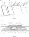
- FIG. 1 is a schematic structural diagram of an electronic device 100 according to some embodiments of this application
- FIG. 2 is an exploded view of the electronic device 100 shown in FIG. 1
- the electronic device 100 is a mobile phone.
- the electronic device 100 includes a screen 10, a back housing 20, a main circuit board 30, a mainboard bracket 40, a camera module 50, and a camera decoration cover 60.
- FIG. 1 and FIG. 2 schematically show merely some components included in the electronic device 100, and actual shapes, sizes, positions, and structures of such components are not limited by FIG. 1 and FIG. 2 .
- the electronic device 100 may not include the screen 10 and/or the mainboard bracket 40.
- the screen 10 is configured to display an image, a video, and the like.
- the screen 10 includes a light-transmitting plate 101 and a display screen 102.
- the light-transmitting plate 101 and the display screen 102 are stacked and fixedly connected.
- the light-transmitting plate 101 is mainly configured to provide a protection and dustproof function for the display screen 102.
- the material of the light-transmitting plate 101 includes but is not limited to glass, ceramic, or plastic.
- the display screen 102 may be a flexible display screen, or may be a rigid display screen.
- the display screen 102 may be an organic light-emitting diode (organic light-emitting diode, OLED) display screen, an active-matrix organic light-emitting diode (active-matrix organic light-emitting diode, AMOLED) display screen, a mini organic light-emitting diode (mini organic light-emitting diode) display screen, a micro organic light-emitting diode (micro organic light-emitting diode) display screen, a micro organic light-emitting diode (micro organic light-emitting diode) display screen, a quantum dot light emitting diodes (quantum dot light emitting diodes, QLED) display screen, or a liquid crystal display (liquid crystal display, LCD) display screen.
- OLED organic light-emitting diode
- AMOLED active-matrix organic light-emitting diode
- mini organic light-emitting diode mini organic light-emitting diode
- the back housing 20 is configured to protect electronic components inside the electronic device 100.
- the back housing 20 includes a rear cover 201 and a frame 202.
- the rear cover 201 is located on one side of the display screen 102 far away from the light-transmitting plate 101, and the light-transmitting plate 101, the display screen 102, and the rear cover 201 are stacked.
- the frame 202 is located between the rear cover 201 and the light-transmitting plate 101.
- the frame 202 is fixed to the rear cover 201.
- the frame 202 may be fixedly connected to the rear cover 201 in a manner such as adhesion, welding, or snap-fit.
- the frame 202 and the rear cover 201 may be integrally formed, that is, the frame 202 and the rear cover 201 are formed as a whole.
- the light-transmitting plate 101 may be fixed to the frame 202 in a manner of adhesion.
- the light-transmitting plate 101, the rear cover 201, and the frame 202 form an internal accommodation space of the electronic device 100.
- the display screen 102 is accommodated in the internal accommodation space.
- a stacking direction of the light-transmitting plate 101, the display screen 102, and the rear cover 201 in the electronic device 100 is defined as a Z-axis direction, and the Z-axis direction may also be referred to as a thickness direction of the electronic device.
- a plane parallel to the light-transmitting plate 101, the display screen 102, and the rear cover 201 is an XY plane. It may be understood that, a coordinate system of the electronic device 100 may be flexibly set according to specific actual requirements. This is not specifically limited herein.
- a direction from the rear cover 201 to the display screen 102 is a forward direction
- a direction from the display screen 102 to the rear cover 201 is a backward direction.
- the main circuit board 30 is fixed in the internal accommodation space of the electronic device 100.
- the main circuit board 30 may be fixed to the display screen 102 in a manner such as threaded connection or snap-fit.
- the main circuit board 30 may be fixed to a surface of the display screen 102 facing the rear cover 201.
- the electronic device 100 further includes a middle plate 70.
- the middle plate 70 is fixed to a circumference of an inner surface of the frame 202.
- the middle plate 70 may be fixed to the frame 202 in a manner of welding, snap-fit, or adhesion.
- the middle plate 70 and the frame 202 may also be integrally formed.
- the middle plate 70 is used as a structural "skeleton" of the electronic device 100, and the main circuit board 30 may be fixed to the middle plate 70 in a manner such as threaded connection, snap-fit, or welding. Specifically, The main circuit board 30 may be fixed to one side of the middle plate 70 facing the rear cover 201.
- the main circuit board 30 may be a rigid circuit board, or a flexible circuit board, or may be a rigid-flex circuit board.
- the main circuit board 30 may be an FR-4 dielectric plate, or a Rogers (Rogers) dielectric plate, or may be a hybrid FR-4 and Rogers dielectric plate, or the like.
- FR-4 is a code name of a flame-resistant material grade
- the Rogers dielectric plate is a high-frequency plate.
- the mainboard bracket 40 is located on one side of the main circuit board 30 facing the rear cover 201, and the mainboard bracket 40 is configured to cover electronic components on the main circuit board 30.
- the mainboard bracket 40 is relatively fixed to the main circuit board 30.
- the mainboard bracket 40 may be fixed to the main circuit board 30 in a manner such as threaded connection, snap-fit, or adhesion, or may be fixed to the middle plate 70 in a manner such as threaded connection, snap-fit, or adhesion.
- the main circuit board 30 may also be fixed to the display screen 102, and the mainboard bracket 40 is fixed to the display screen 102 in a manner such as threaded connection, snap-fit, or adhesion.
- the mainboard bracket 40 may be fixed to the surface of the display screen 102 facing the rear cover 201. In this way, the main circuit board 30 may be connected to the display screen 102 by using the mainboard bracket 40.
- the material of the mainboard bracket 40 includes but is not limited to plastic, metal, or a combination of plastic and metal.
- the camera module 50 is configured to capture photos/record videos.
- the camera module 50 may be a camera module having at least one of the following functions: adjusting a light entering amount, automatic focusing (automatic focusing, AF), or optical image stabilization (optical image stabilization, OIS).
- the camera module 50 may be an automatic focusing camera module 50.
- the camera module 50 may also be a camera module that does not have functions such as adjusting a light entering amount, automatic focusing (automatic focusing, AF), and optical image stabilization (optical image stabilization, OIS).
- the camera module 50 may be a fixed-focus camera module.
- the fixed-focus camera module includes but is not limited to a wide-angle camera module or a macro camera module.
- the camera module 50 is used as a rear camera module of the electronic device 100.
- the camera module 50 may include one camera, or may include an array including a plurality of cameras.
- the camera module 50 is fixed in the internal accommodation space of the electronic device 100.
- the camera module 50 may be fixed to the display screen 102 in a manner such as threaded connection, snap-fit, or welding.
- the camera module 50 may be fixed to the surface of the display screen 102 facing the rear cover 201, and a light-incident surface 5021 of the camera module 50 faces the rear cover 201.
- the camera module 50 may be fixed to the middle plate 70 in a manner such as threaded connection, snap-fit, or welding.
- the camera module 50 may be fixed to the surface of the middle plate 70 facing the rear cover 201.
- the camera module 50 may be fixed to a surface of the main circuit board 30 facing the rear cover 201.
- At least part of the camera module 50 may be located between the main circuit board 30 and the mainboard bracket 40, the mainboard bracket 40 is covered on the camera module 50, and the mainboard bracket 40 is provided with an avoidance hole 401 corresponding to the camera module 50, to help the camera module 50 receive a light ray.
- An avoidance through hole 301 is provided on the main circuit board 30 at a position corresponding to the camera module 50, and an end of the camera module 50 far away from the rear cover 201 is located in the avoidance through hole 301 of the main circuit board 30.
- the camera module 50 and the main circuit board 30 have an overlapping region in the Z-axis direction, to prevent the camera module 50 from being stacked on the main circuit board 30 to increase a thickness of the electronic device 100 in the Z-axis direction.
- the camera module 50 is electrically connected to the main circuit board 30. In this way, the camera module 50 may receive signals from the main circuit board 30, and may also transmit signals to the main circuit board 30.
- FIG. 3 is a schematic cross-sectional view of a partial structure of the electronic device 100 shown in FIG. 1 and FIG. 2 .
- the camera module 50 includes: a housing 501, an optical lens 502, a driving motor 503, a variable aperture 504, a circuit board 505, and an image sensor 506.
- the housing 501 is configured to connect the optical lens 502, the driving motor 503, the variable aperture 504, the circuit board 505, and the image sensor 506 as a whole, and fix the whole in the internal accommodation space of the electronic device 100.
- the material of the housing 501 includes but is not limited to plastic, metal, or a combination of plastic and metal.
- the material of the housing 501 includes but is not limited to aluminum alloy or magnesium-aluminum alloy.
- the optical lens 502 is located in the housing 501.
- the optical lens 502 includes an optical lens set and a lens barrel, where the optical lens set includes at least one optical lens.
- the optical lens set includes a plurality of optical lenses
- the plurality of optical lenses are stacked in an optical-axis direction.
- the lens barrel is configured to fix and protect the optical lens set.
- the lens barrel has a cylindrical structure. That is, both ends of the lens barrel are open in the optical-axis direction.
- the optical lens set is mounted in the lens barrel.
- the optical lens set is mounted in the driving motor 503 in the housing 501 by using the lens barrel.
- the optical lens may not include the lens barrel, and the driving motor 503 and the optical lens set are integrated, which can reduce the volume of the camera module 50.
- the optical lens 502 having different features such as wide-angle, standard, and telephoto may be obtained by designing the structural composition of the optical lens set and the shape and size of each optical lens.
- the optical lens 502 includes a light-incident surface 5021 and a light exit surface 5022. During use of the optical lens 502, a light ray is emitted into the optical lens 502 through the light-incident surface 5021 and is emitted out through the light exit surface 5022.
- the camera module 50 is a vertical camera module, and the optical lens 502 is a vertical lens.
- An optical axis of the vertical lens extends in the Z-axis direction, the light-incident surface 5021 of the optical lens 502 faces a photographed scenery, and the light exit surface 5022 of the optical lens 502 faces away from the photographed scenery.
- the camera module 50 is a periscopic camera module.
- An optical lens 502 of the periscopic camera module is a periscopic lens, and an optical axis of the periscopic lens is parallel to the XY plane. It is to be noted that, The following embodiments are described by using an example in which the camera module 50 is the periscopic camera module, but this cannot be construed as a particular limitation on this application.
- the driving motor 503 is configured to drive the optical lens 502 to move, to achieve automatic focusing and/or optical image stabilization. Specifically, The driving motor 503 may only be configured to drive the optical lens 502 to move in the Z-axis direction, to achieve automatic focusing. Alternatively, the driving motor 503 may only be configured to drive the optical lens 502 to move on the XY plane or tilt in any direction around the optical axis of the optical lens 502, to achieve optical image stabilization. In addition, the driving motor 503 may be configured to achieve both automatic focusing and optical image stabilization.
- variable aperture 504 is located on one side of the light-incident surface 5021 of the optical lens 502.
- the variable aperture 504 includes an aperture hole 5041, where the aperture hole 5041 is opposite to the light-incident surface 5021 of the optical lens 502. Alight ray is emitted into the optical lens 502 through the aperture hole 5041.
- the size of the aperture hole 5041 is changeable to adjust the light entering amount of the optical lens 502.
- the image sensor 506 is located on a light emitting side of the optical lens 502, and a light sensing surface of the image sensor 506 is opposite to the light exit surface 5022 of the optical lens 502.
- the image sensor 506 is configured to collect light rays emitted through the optical lens 502 and convert image information carried by the light rays into an electrical signal.
- the image sensor 506 is electrically connected to the circuit board 505, and the image sensor 506 may transmit the electrical signal to the main circuit board 30 through the circuit board 505.
- the circuit board 505 is located on one side of the housing 501 far away from the mounting opening 2011, the circuit board 505 may be fixed to the driving motor 503, and the image sensor 506 may be arranged on one side of the circuit board 505 facing the optical lens 502.
- the circuit board 505 may be fixed to the driving motor 503 in a manner such as snap-fit, threaded connection, or adhesion.
- the circuit board 505 may be a rigid circuit board, or a flexible circuit board, or may be a rigid-flex circuit board.
- the circuit board 505 may be an FR-4 dielectric plate, or a Rogers (Rogers) dielectric plate, or may be a hybrid FR-4 and Rogers dielectric plate, or the like.
- FR-4 is a code name of a flame-resistant material grade
- the Rogers dielectric plate is a high-frequency plate.
- the mounting opening 2011 is provided on the rear cover 201 at a position corresponding to the camera module 50. There may be one mounting opening 2011, or there may be a plurality of mounting openings 2011. In some examples, all camera modules 50 correspond to one mounting opening 2011. In some other examples, the camera module 50 and the mounting opening 2011 have the same quantity and are in a one-to-one correspondence.
- the camera decoration cover 60 is relatively fixed to the rear cover 201.
- the camera decoration cover 60 corresponds to the mounting opening 2011 and protects the camera module 50.
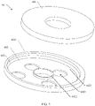
- FIG. 4 is an exploded view of a camera decoration cover 60 of the electronic device 100 shown in FIG. 1 to FIG. 3 .
- the camera decoration cover 60 includes a light-transmitting cover plate 601, a decoration cover plate 602, and an adhesive layer 603.
- the decoration cover plate 602 is arranged on the rear cover 201.
- the decoration cover plate 602 may be mounted on one side of the rear cover 201 far away from the light-transmitting plate 101 and cover the mounting opening 2011.
- the decoration cover plate 602 may be located in the mounting opening 2011.
- the decoration cover plate 602 is located at an end of the mounting opening 2011 adjacent to the camera module 50 and covers the mounting opening 2011.
- the connection manner between the decoration cover plate 602 and the rear cover 201 includes but is not limited to adhesion, snap-fit, welding, or screw connection.
- a sealing member (not shown in the figure) is arranged between the decoration cover plate 602 and the rear cover 201. Based on the arrangement of the sealing member, sealing performance between the decoration cover plate 602 and the rear cover 201 may be improved.
- the sealing member includes but is not limited to a sealant, a rubber sealing ring, a silicone sealing ring, or the like. Further, A sealing groove (not shown in the figure) configured to accommodate the sealing member may also be provided on one of the decoration cover plate 602 or the rear cover 201.
- the decoration cover plate 602 is provided with a camera hole 6023, and there may be one or more camera holes 6023.
- the camera hole 6023 corresponds to the mounting opening 2011. In some examples, in a case that there are a plurality of camera holes 6023, all camera holes 6023 correspond to one mounting opening 2011. In some other examples, the camera hole 6023 and the mounting opening 2011 have the same quantity and are in a one-to-one correspondence.
- the camera hole 6023 and the camera module 50 have the same quantity and are in a one-to-one correspondence.
- the camera hole 6023 is right opposite to the corresponding camera module 50, and the light ray is allowed by the camera hole 6023 to be emitted into the light-incident surface 5021 of the optical lens 502.
- one camera hole 6023 corresponds to a plurality of camera modules 50.
- the material of the decoration cover plate 602 includes but is not limited to plastic, metal, or a combination of plastic and metal. In this embodiment of this application, the material of the decoration cover plate 602 may be plastic, reduce costs and reduce the weight of the electronic device 100.
- the shape of the decoration cover plate 602 includes but is not limited to a square, a rectangular, a circle, an ellipse, or a special shape.
- FIG. 5 is an exploded view of a camera decoration cover 60 according to some other embodiments of this application.
- the shape of the decoration cover plate 602 may also in the shape of a ring, and the camera hole 6023 is provided between an inner edge and an outer edge of the ring-shaped decoration cover plate 602.
- the shape of the decoration cover plate 602 includes but is not limited to a square ring, a rectangular ring, a circular ring, an elliptical ring, or a special circular ring.
- a first flange 6021 may be arranged on an outer peripheral wall of the decoration cover plate 602, the first flange 6021 may be in the shape of a ring extending fully around a circumferential direction of the decoration cover plate 602, and the first flange 6021 protrudes in a direction away from the camera module 50.
- the first flange 6021 may be fixed to the outer peripheral wall of the decoration cover plate 602 in a manner of welding or adhesion.
- the first flange 6021 may also be integrally formed with the decoration cover plate 602. It may be understood that the outer peripheral wall of the decoration cover plate 602 may not include the first flange 6021.
- a second flange 6022 may further be arranged on an inner peripheral wall of the decoration cover plate 602, the second flange 6022 may be in the shape of a ring extending fully around the circumferential direction of the decoration cover plate 602, and the second flange 6022 in the direction away from the camera module 50.
- the second flange 6022 may be fixed to the inner peripheral wall of the decoration cover plate 602 in a manner of welding or adhesion.
- the second flange 6022 may also be integrally formed with the decoration cover plate 602. It may be understood that the inner peripheral wall of the decoration cover plate 602 may not include the second flange 6022.
- the light-transmitting cover plate 601 is located on one side of the decoration cover plate 602 far away from the camera module 50, and the light-transmitting cover plate 601 and the decoration cover plate 602 are stacked and fixed to each other, so that the light-transmitting cover plate 601 covers at least part of the decoration cover plate 602, that is, the light-transmitting cover plate 601 may partially cover the decoration cover plate 602, or the light-transmitting cover plate 601 may entirely cover the decoration cover plate 602.
- a region on the decoration cover plate 602 covered by the light-transmitting cover plate 601 is a coverage region 6025, and the camera hole 6023 is located in the coverage region 6025.
- the light ray may pass through the light-transmitting cover plate 601 and is emitted into the light-incident surface 5021 of the camera module 50 through the camera hole 6023.
- the light-transmitting cover plate 601 may protect the camera module 50 from water and dust.
- the material of the light-transmitting cover plate 601 includes but is not limited to glass, a plastic member, or ceramics.
- the light-transmitting cover plate 601 may be a light filter having a function of light filtering, so that the light-transmitting cover plate 601 may replace a light filter in the camera module 50 to play a role of light filtering, and the light filter in the camera module 50 can be omitted, thereby reducing the volume of the camera module 50.
- the light-transmitting cover plate 601 may be formed as a square, a rectangular, a circle, an ellipse, or a special shape. Specifically, An outer edge of the light-transmitting cover plate 601 coincides with the outer edge of the decoration cover plate 602 in the XY plane, so that an outer edge of the coverage region 6025 coincides with the outer edge of the decoration cover plate 602.
- the light-transmitting cover plate 601 may also be ring-shaped, so that the coverage region 6025 on the decoration cover plate 602 covered by the light-transmitting cover plate 601 is also ring-shaped.
- the light-transmitting cover plate 601 may be formed as a square ring, a rectangular ring, a circular ring, an elliptical ring, or a special circular ring.
- the outer edge of the light-transmitting cover plate 601 coincides with the outer edge of the decoration cover plate 602 in the XY plane, and an inner edge of the light-transmitting cover plate 601 also coincides with the inner edge of the decoration cover plate 602 in the XY plane, so that the outer edge of the coverage region 6025 coincides with the outer edge of the decoration cover plate 602 in the XY plane, and an inner edge of the coverage region 6025 coincides with the inner edge of the decoration cover plate 602 in the XY plane.
- the light-transmitting cover plate 601 is located on an inner peripheral side of the first flange 6021, so that mounting of the light-transmitting cover plate 601 and the decoration cover plate 602 may be positioned by using the first flange 6021, and the light-transmitting cover plate 601 may also be limited by using the first flange 6021.
- the light-transmitting cover plate 601 may be ring-shaped, and the light-transmitting cover plate 601 is located between the first flange 6021 and the second flange 6022.
- the mounting of the light-transmitting cover plate 601 and the decoration cover plate 602 may be positioned by using the first flange 6021 and the second flange 6022, and the light-transmitting cover plate 601 may also be limited by using the first flange 6021 and the second flange 6022.
- this application is not limited thereto.
- the light-transmitting cover plate 601 may not be ring-shaped and the light-transmitting cover plate 601 no longer includes the second flange 6022, and the light-transmitting cover plate 601 covers a through hole defined by the decoration cover plate 602, the camera hole 6023, and the inner edge of the decoration cover plate 602.
- the light-transmitting cover plate 601 and the coverage region 6025 of the decoration cover plate 602 are adhered to each other through the adhesive layer 603.
- the adhesive layer 603 is located in the coverage region 6025, the adhesive layer 603 is in the shape of a ring extending fully around a circumferential direction of the coverage region 6025, and the camera hole 6023 is located on an inner peripheral side of the adhesive layer 603.
- the adhesive layer 603 may connect the light-transmitting cover plate 601 and the decoration cover plate 602 in the entire circumferential direction of the coverage region 6025, thereby improving reliability of connection between the light-transmitting cover plate 601 and the decoration cover plate 602.
- the adhesive layer 603 can discharge static electricity for the camera module 50 to some extent, static electricity on an outer surface of the camera decoration cover 60 may generally flow into a region between the coverage region 6025 and the light-transmitting cover plate 601 through a gap between an edge of the coverage region 6025 and the light-transmitting cover plate 601.
- static electricity on an outer surface of the camera decoration cover 60 may generally flow into a region between the coverage region 6025 and the light-transmitting cover plate 601 through a gap between an edge of the coverage region 6025 and the light-transmitting cover plate 601.
- more camera holes 6023 provided on the decoration cover plate 602 and occupies more space on the decoration cover plate 602.
- a shortest electrostatic discharge path (an electrostatic discharge path indicated by a dashed arrow A1 in FIG. 3 ) is a metal structure discharged into the camera module 50, for example, the driving motor 503, and/or a metal housing 501, which is likely to damage the camera module 50.
- the mainboard bracket 40 since one part of the mainboard bracket 40 is adjacent to the camera hole 6023, the mainboard bracket 40 is configured as a metal member and configured to be grounded. In this way, static electricity introduced into the electronic device 100 from the camera hole 6023 may be discharged by using the mainboard bracket 40.
- the structure of the mainboard bracket 40 is complex and huge, the weight of a metal mainboard bracket 40 is relatively heavy, and costs is high.
- a conductive fabric or copper foil may also be arranged on an inner peripheral wall of the camera hole 6023, the conductive fabric or the copper foil is grounded, and static electricity at the camera hole 6023 is discharged by using the conductive fabric or the copper foil. Processing costs of such a manner is relatively high.
- Static electricity can be discharged to some extent by using the foregoing two implementations, but in the two implementations, static electricity needs to be guided to the camera hole 6023 for discharge. Since the camera hole 6023 is right opposite to the camera module 50, static electricity at the camera hole 6023 that is not discharged is still easily guided to the camera module 50, causing failure of the camera module 50.
- FIG. 6 is a schematic cross-sectional view of a partial structure of an electronic device 100 according to some other embodiments of this application
- FIG. 7a is a schematic structural diagram of a decoration cover plate 602 of the electronic device 100 shown in FIG. 6 .
- the coverage region 6025 includes at least one first region 60251, and the first region 60251 is provided with at least one first static electrostatic discharge hole 6024 corresponding to the camera hole 6023.
- each camera hole 6023 may include at least one corresponding first region 60251, and the first region 60251 is provided with at least one first electrostatic discharge hole 6024.
- At least one first region 60251 may be arranged for some camera holes 6023, the first region 60251 is provided with at least one first electrostatic discharge hole 6024, the first electrostatic discharge hole 6024 is configured for anti-static and protects the camera module 50 in the corresponding camera hole 6023, and other camera holes 6023 do not include the first region 60251 and the first electrostatic discharge hole 6024.
- the at least one first electrostatic discharge hole 6024 is spaced apart from the corresponding camera hole 6023.
- the at least one first electrostatic discharge hole 6024 corresponds to a first ground member 80.
- the first ground member 80 and the camera module 50 are independent of each other and the first ground member 80 is grounded.
- the one first electrostatic discharge hole 6024 simultaneously corresponds to a plurality of first ground members 80.
- all first electrostatic discharge holes 6024 may correspond to one first ground member 80.
- different first electrostatic discharge holes 6024 respectively correspond to first ground members 80 with different quantities.
- different first ground members 80 respectively correspond to first electrostatic discharge holes 6024 with different quantities.
- the plurality of first ground members 80 and the plurality of first electrostatic discharge holes 6024 are in a one-to-one correspondence.
- the first ground member 80 may be shared between first electrostatic discharge holes 6024 corresponding to different camera holes 6023.
- the first electrostatic discharge holes 6024 corresponding to different camera holes 6023 correspond to different first ground members 80.
- a center of the coverage region 6025 is a first center o1, and a center of the camera hole 6023 is a second center o2.
- the "first center o1" may be a centroid, a center of gravity, or a center of mass of the coverage region 6025.
- the “second center o2" may be a centroid, a center of gravity, or a center of mass of the camera hole 6023.
- the shapes of the coverage region 6025 and the camera hole 6023 include but are not limited to a circle, a square, a rectangular, a regular polygon, a polygon, or another irregular shape meeting assembly or use requirements.
- the first center o1 is spaced apart from the second center o2, that is, the second center o2 of the camera hole 6023 deviates from the first center o1 of the coverage region 6025.
- a straight line where the first center o1 and the second center o2 lie is a straight line L1.
- the first region 60251 is a region formed on one side of the second center o2 far away from the first center o1 by respectively rotating the straight line L1 around the first center o1 toward two sides of the straight line L1 by a first preset angle ⁇ .
- a straight line L11 is obtained by clockwise rotating the straight line L1 around the first center o1 by the first preset angle ⁇ .
- a straight line L12 is obtained by counterclockwise rotating the straight line L1 around the first center o1 by the first preset angle ⁇ .
- a region located on one side of the second center o2 far away from the first center o1 and between the straight line L11 and the straight line L12 is the first region 60251, and the at least one first electrostatic discharge hole 6024 is located in the first region 60251.
- the first preset angle ⁇ is in a range of (0, 45°].
- the value of the first preset angle ⁇ is 28°, 30°, 32° 35°, 37°, or 40°.
- a straight line perpendicular to the straight line L1 is a straight line L2.
- the straight line L2 passes through the second center o2.
- the straight line L11 is obtained by clockwise rotating the straight line L1 around the first center o1 by the first preset angle ⁇ .
- the straight line L12 is obtained by counterclockwise rotating the straight line L1 around the first center o1 by the first preset angle ⁇ .
- a region in the coverage region 6025 located on one side of the straight line L2 far away from the first center o1 and between the straight line L11 and the straight line L12 is the first region 60251 (which is a region indicated by a shaded part in FIG. 7a ), and the at least one first electrostatic discharge hole 6024 is located in the first region 60251.
- FIG. 7b is a schematic structural diagram of a decoration cover plate 602 of the electronic device 100 shown in FIG. 6 .
- a circle with the first center o1 as a center of a circle and a distance between the first center o1 and the second center o2 as a radius is a circle c1.
- the straight line L11 is obtained by clockwise rotating the straight line L1 around the first center o1 by the first preset angle ⁇ .
- the straight line L12 is obtained by counterclockwise rotating the straight line L1 around the first center o1 by the first preset angle ⁇ .
- a region in the coverage region 6025 located between the straight line L11 and the straight line L12, and between an edge of the circle c1 and an outer edge of the coverage region 6025 is the first region 60251 (which is a region indicated by a shaded part in FIG. 7b ), and the at least one first electrostatic discharge hole 6024 is located in the first region 60251.
- the division of an edge of the first region 60251 adjacent to one side of the first center o1 is not limited to the forms of the straight line L2 and the circle c1 involved in the foregoing embodiments.
- the edge of the first region 60251 adjacent to one side of the first center o1 may alternatively be formed by one part of a boundary line in any shape that is centered on the first center o1 and passes through the second center o2.
- the first region 60251 is a region formed on one side of the second center o2 far away from the first center o1 by respectively rotating the straight line L1 around the first center o1 toward two sides of the straight line L1 by a first preset angle ⁇ , where the first preset angle ⁇ is in a range of (0, 45°], and at least one first electrostatic discharge hole 6024 corresponding to the camera hole 6023 is provided in the first region 60251, so that the first electrostatic discharge hole 6024 may be distributed at a position on a periphery of the camera hole 6023 close to the outer edge of the coverage region 6025, and static electricity located on an outer side of the electronic device 100 first passes through the first electrostatic discharge hole 6024 and then is discharged to the first ground member 80 without being discharged to the camera module 50 through the camera hole 6023.
- first ground member 80 and the camera module 50 are independent of each other (that is, the first ground member 80 is not one part of the camera module 50, and the camera module 50 is not one part of the first ground member 80), so that at least part of the static electricity located on the outer side of the electronic device 100 may not damage the camera module 50, thereby improving a protection effect on the camera module 50.
- the first preset angle ⁇ is in a range of (0, 25°].
- the value of the first preset angle ⁇ is 10°, 12°, 15°, 18°, 20°, 22°, or 25°.
- the position of the first electrostatic discharge hole 6024 in the first region 60251 may further be optimized, so that it can be further ensured that the static electricity located on the outer side of the electronic device 100 first passes through the first electrostatic discharge hole 6024 and then is discharged to the first ground member 80 without being discharged to the camera module 50 through the camera hole 6023, thereby improving the protection effect on the camera module 50.
- the first electrostatic discharge hole 6024 may be provided between the periphery of the camera hole 6023 and the outer edge of the coverage region 6025.
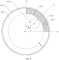
- FIG. 8 is a schematic structural diagram of the decoration cover plate 602 shown in FIG. 7a .
- the coverage region 6025 includes a first subregion 60252, and the first subregion 60252 is connected to the outer edge of the coverage region 6025.
- an outer edge of the first subregion 60252 coincides with the outer edge of the coverage region 6025, an inner edge of the first subregion 60252 (a dotted circle as shown in FIG.
- the first subregion 60252 is in the shape of a ring extending fully around the circumferential direction of the coverage region 6025, so that the first subregion 60252 and the first region 60251 have an overlapping region (which is a region indicated by a shaded part in FIG. 8 ), and the at least one first electrostatic discharge hole 6024 is located in the overlapping region.
- a distance d between the inner edge of the first subregion 60252 and the outer edge of the coverage region 6025 is in a range of (0, 10 mm].
- the distance d between the inner edge of the first subregion 60252 and the outer edge of the coverage region 6025 is 1 mm, 1.5 mm, 2 mm, 2.5 mm, 3 mm, 3.5 mm, 4 mm, 4.5 mm, 5 mm, 5.5 mm, 6 mm, 6.5 mm, 7 mm, 7.5 mm, 8 mm, 8.5 mm, or 9 mm.
- FIG. 9 is a schematic structural diagram of the decoration cover plate 602 shown in FIG. 7a .
- the at least one first electrostatic discharge hole 6024 is located on an outer side of an orthographic projection (for example, a dashed box B1 in FIG. 9 ) of the corresponding camera module 50 in the coverage region 6025.
- the orthographic projection of the camera module 50 in the coverage region 6025 is the dashed box B1
- the at least one first electrostatic discharge hole 6024 corresponding to the camera module 50 is located on an outer side of the dashed box B1.
- the first electrostatic discharge hole 6024 may be provided to be farther from the camera module 50 in the XY plane, so that the position of the first electrostatic discharge hole 6024 is further optimized, thereby improving the electrostatic protection effect on the camera module 50.
- the "orthographic projection" of any component in the coverage region 6025 mentioned in this application is a projection in a thickness direction (that is, the Z-axis direction) of the electronic device 100.
- each camera hole 6023 corresponds to a plurality of first electrostatic discharge holes 6024, and the first electrostatic discharge holes 6024 are respectively provided on two sides of the straight line L1.
- Such configuration is beneficial to arrange the first electrostatic discharge hole 6024 according to the position of the camera module 50 and the layout of the first ground member 80 inside the electronic device 100, thereby improving rationality of the structural layout.
- an outer peripheral profile of the coverage region 6025 is a circle
- the orthographic projection of the camera module 50 in the coverage region 6025 (for example, the rectangular dashed box B1 in FIG. 9 ) is a rectangle
- the straight line L1 passes through one of diagonals of the orthographic projection of the camera module 50, so that a minimum distance between an edge of the camera hole 6023 and the outer edge of the coverage region 6025 is the size of a portion of the straight line L1 located between the edge of the camera hole 6023 and the outer edge of the coverage region 6025
- first electrostatic discharge holes 6024 are respectively provided on two sides of the straight line L1 in the circumferential direction of the coverage region 6025, and the first electrostatic discharge holes 6024 are located on the outer side of the orthographic projection of the camera module 50 in the coverage region 6025.
- the first electrostatic discharge hole 6024 is provided on the outer side of the orthographic projection of the camera module 50 in the coverage region 6025, to ensure that the first electrostatic discharge hole 6024 is provided to be farther from the camera module 50 in the XY plane, thereby improving electrostatic protection capability for the camera module 50, the first electrostatic discharge hole 6024 may be provided larger by fully using a space of the coverage region 6025, thereby improving rationality of the structural layout and further improving the electrostatic protection effect on the camera module 50.
- FIG. 10 is a schematic structural diagram of a decoration cover plate 602 according to some other embodiments of this application.
- the at least one first electrostatic discharge hole 6024 intersects with the straight line L1.
- the camera hole 6023 deviates from the first center o1 of the coverage region 6025, a distance between the camera hole 6023 corresponding to the straight line L1 and the outer edge of the coverage region 6025 is relatively small.
- the electrostatic discharge path may be shortened, thereby facilitating timely discharge of static electricity.
- the outer peripheral profile of the coverage region 6025 is circular, the minimum distance between the edge of the camera hole 6023 and the outer edge of the coverage region 6025 corresponds to the size of the portion of the straight line L1 located between the edge of the camera hole 6023 and the outer edge of the coverage region 6025, the camera hole 6023 corresponds to one first electrostatic discharge hole 6024, and the one first electrostatic discharge hole 6024 intersects with the portion of the straight line L1 located between the edge of the camera hole 6023 and the outer edge of the coverage region 6025.
- the electrostatic discharge path may be shortened, thereby facilitating timely discharge of static electricity.
- the first electrostatic discharge hole 6024 is an elongated hole, where the elongated hole extends in the circumferential direction of the coverage region 6025.
- more regions of the camera hole 6023 may be surrounded by the first electrostatic discharge hole 6024 in the circumferential direction of the coverage region 6025, so that it is further ensured that static electricity can be discharged to the first ground member 80 through the first electrostatic discharge hole 6024 in time, thereby improving the electrostatic protection effect on the camera module 50.
- the elongated hole may extend in an arc, a straight line, or an irregular curve as long as the elongated hole extends in the circumferential direction of the coverage region 6025.
- FIG. 11 is a schematic diagram of a connection between the decoration cover plate 602 shown in FIG. 9 and an adhesive layer 603 and a protruding adhesive layer portion 6031.
- the first electrostatic discharge hole 6024 is located on an inner peripheral side of the adhesive layer 603, and the protruding adhesive layer portion 6031 is arranged on an inner edge of the adhesive layer 603.
- the protruding adhesive layer portion 6031 protrudes toward the camera hole 6023, and the protruding adhesive layer portion 6031 is located in the first region 60251.
- the adhesive layer 603 has a certain anti-static effect, and the arrangement of the protruding adhesive layer portion 6031 may widen the width of the adhesive layer 603 on the protruding adhesive layer portion 6031. In this way, the electrostatic protection effect on the camera module 50 is further improved by using protruding adhesive layer portion 6031 while the anti-static effect on the camera module 50 is achieved through cooperation between the first electrostatic discharge hole 6024 and the first ground member 80.
- each camera hole 6023 corresponds to a plurality of first electrostatic discharge holes 6024, and the protruding adhesive layer portion 6031 is provided with the first electrostatic discharge holes 6024 respectively on two sides of a circumferential direction of the camera hole 6023.
- Such configuration is beneficial to arrange the first electrostatic discharge hole 6024 according to the position of the camera module 50 and the layout of the first ground member 80 inside the electronic device 100, thereby improving rationality of the structural layout.
- the decoration cover plate 602 may only include the protruding adhesive layer portion 6031, and there is no first electrostatic discharge hole 6024 arranged.
- the protruding adhesive layer portion 6031 and the adhesive layer 603 may be integrated. Certainly, this application is not limited thereto. In other embodiments, the protruding adhesive layer portion 6031 may also be adhered to the adhesive layer 603.
- the camera decoration cover 60 is covered on the mounting opening 2011, the camera decoration cover 60 is located on one side of the rear cover 201 far away from the camera module 50, a first via hole 2012 is provided on a portion of the rear cover 201 corresponding to the coverage region 6025, an orthographic projection of the first via hole 2012 in the coverage region 6025 overlaps the first electrostatic discharge hole 6024, and static electricity introduced by the first electrostatic discharge hole 6024 is guided to the first ground member 80 through the first via hole 2012.
- an orthographic projection of the first via hole 2012 in the coverage region 6025 completely overlaps (or coincides with each other) the first electrostatic discharge hole 6024.
- an outer edge of the orthographic projection of the first via hole 2012 in the coverage region 6025 is the same as and consistent with an outer edge of the first electrostatic discharge hole 6024.
- the orthographic projection of the first via hole 2012 in the coverage region 6025 partially overlaps the first electrostatic discharge hole 6024.
- one part of the orthographic projection of the first via hole 2012 in the coverage region 6025 is located within the first electrostatic discharge hole 6024.
- the orthographic projection of the first via hole 2012 in the coverage region 6025 is located within the first electrostatic discharge hole 6024.
- the entire first electrostatic discharge hole 6024 or one part of the first electrostatic discharge hole 6024 is located in the orthographic projection of the first via hole 2012 in the coverage region 6025.
- the first via hole 2012 is provided, and the orthographic projection of the first via hole 2012 in the coverage region 6025 overlaps the first electrostatic discharge hole 6024, so that the first via hole 2012 may be in communication with the first electrostatic discharge hole 6024, and the electrostatic discharge path may be shortened, thereby facilitating timely discharge of static electricity to the first ground member 80 through the first electrostatic discharge hole 6024 and the first via hole 2012.
- overlap between A and B in any two shape (for example, A is the orthographic projection of the first via hole 2012 in the coverage region 6025, and B is the first electrostatic discharge hole 6024) mentioned in this application includes full overlap (that is, coincidence) between A and B and partial overlap between A and B.
- the full overlap between A and B means that an outer edge of A is the same as and consistent with an outer edge of B.
- the partial overlap means that A is located inside the outer edge of B, or one part of A is located inside the outer edge ofB and the other part of A is located outside the outer edge of B; or B is located inside the outer edge of A, or one part ofB is located inside the outer edge of A and the other part of B is located outside the outer edge of A.
- a second via hole 402 is provided on the mainboard bracket 40, and the orthographic projection of the first via hole 2012 in the coverage region 6025 overlaps an orthographic projection of the second via hole 402 in the coverage region 6025.
- the orthographic projection of the first via hole 2012 in the coverage region 6025 completely overlaps the orthographic projection of the second via hole 402 in the coverage region 6025.
- the orthographic projection of the first via hole 2012 in the coverage region 6025 partially overlaps the orthographic projection of the second via hole 402 in the coverage region 6025.
- the first via hole 2012 may be in communication with the second via hole 402, thereby facilitating timely discharge of static electricity to the first ground member 80 through a discharge path including the first electrostatic discharge hole 6024, the first via hole 2012, and the second via hole 402 (which is an electrostatic discharge path indicated by a dashed arrow A2 in FIG. 6 ).
- FIG. 12 is a schematic cross-sectional view of a partial structure of an electronic device 100 according to yet some other embodiments of this application.
- the decoration cover plate 602 is located inside the mounting opening 2011, and the rear cover 201 does not include a portion corresponding to the decoration cover plate 602
- the first via hole 2012 is no longer provided on the rear cover 201
- the second via hole 402 corresponding to the first electrostatic discharge hole 6024 is directly provided on the mainboard bracket 40.
- the second via hole 402 is provided, thereby facilitating the timely discharge of static electricity to the first ground member 80 through the first electrostatic discharge hole 6024 and the second via hole 402.
- the orthographic projection of the second via hole 402 in the coverage region 6025 overlaps the first electrostatic discharge hole 6024.
- the orthographic projection of the second via hole 402 in the coverage region 6025 completely overlaps the first electrostatic discharge hole 6024.
- the orthographic projection of the second via hole 402 in the coverage region 6025 partially overlaps the first electrostatic discharge hole 6024. With such configuration, the electrostatic discharge path may be shortened.
- the first ground member 80 is mounted on one side of the main circuit board 30 facing the camera decoration cover 60, and orthographic projections of the first ground member 80 and the second via hole 402 in the coverage region 6025 are overlapped. With such configuration, the electrostatic discharge path may be shortened, thereby facilitating timely discharge of static electricity to the first ground member 80.
- the electrostatic discharge path may be significantly shortened.
- the orthographic projections of the first electrostatic discharge hole 6024 and the second via hole 402 in the coverage region 6025, and the orthographic projection of the first ground member 80 in the coverage region 6025 are all overlapped. Therefore, the electrostatic discharge path may be significantly shortened.
- the first ground member 80 is a shielding cover located between the mainboard bracket 40 and the main circuit board 30.
- the first ground member 80 is configured as the shielding cover, and therefore, on the one hand, the shielding cover may play a role of discharging static electricity and protecting the camera module 50; and on the other hand, the shielding cover may be covered on components on the main circuit board 30 and play a role of electromagnetic shielding, so that functions of a shielding cover originally located on the main circuit board 30 may be increased, and there is no need to additionally arrange the first ground member 80, thereby simplifying the structure of the electronic device 100 and reducing production costs.
- FIG. 13 is a schematic cross-sectional view of a partial structure of an electronic device 100 according to still other embodiments of this application.
- one end of the first ground member 80 is mounted on one side of the main circuit board 30 facing the camera decoration cover 60, and the other end of the first ground member 80 extends toward the camera decoration cover 60 and passes through the second via hole 402. Based on such configuration, static electricity is directly discharged to the first ground member 80 protruding from the second via hole 402 without flowing through the second via hole 402, thereby shortening the electrostatic discharge path.
- the first ground member 80 may be constructed as a metal elastic piece, a metal column, or a TVS (transient voltage suppressor) device.
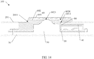
- FIG. 14 is a schematic cross-sectional view of a partial structure of an electronic device 100 according to still other embodiments of this application.
- the mainboard bracket 40 may no longer be provided with the second via hole 402, and instead, at least one part of the mainboard bracket 40 is configured as the first ground member 80. With such configuration, the electrostatic discharge path may be shortened while the structural strength of the mainboard bracket 40 is ensured.
- one part of the mainboard bracket 40 adjacent to the first electrostatic discharge hole 6024 is constructed as the first ground member 80.
- the electrostatic discharge path may be shortened.
- the entire mainboard bracket 40 may be constructed as the first ground member 80 to simplify processes of processing and manufacturing.
- the electrostatic discharge path may be shortened.
- the entire mainboard bracket 40 may be constructed as the first ground member 80 to simplify processes of processing and manufacturing.
- the coverage region 6025 may be formed in the shape of a ring.
- the coverage region 6025 in addition to an outer edge, the coverage region 6025 further includes an inner edge.
- Static electricity on an outer surface of the camera decoration cover 60 may flow into a region between the coverage region 6025 and the light-transmitting cover plate 601 through a gap between the inner edge of the coverage region 6025 and the light-transmitting cover plate 601, and then may be discharged to the camera module 50 through the camera hole 6023, causing damage to the camera module 50.
- Technical solutions are further provided below to resolve the technical problems.
- any technical solution mentioned below may be an improvement made to any one of the foregoing technical solutions based on the first electrostatic discharge hole 6024, or may be a technical solution that does not provide the first electrostatic discharge hole 6024 and is parallel to the technical solution based on the first electrostatic discharge hole 6024.
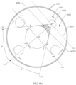
- FIG. 15a is a schematic structural diagram of a decoration cover plate 602 according to yet other embodiments of this application.
- the coverage region 6025 includes at least one second region 60253, where the second region 60253 is provided with at least one second electrostatic discharge hole 6026 corresponding to the camera hole 6023.
- each camera hole 6023 may correspondingly include at least one second region 60253, where the second region 60253 is provided with at least one second electrostatic discharge hole 6026.
- At least one second region 60253 may be correspondingly arranged for some camera holes 6023, where the second region 60253 is provided with at least one second electrostatic discharge hole 6026, and the second electrostatic discharge hole 6026 is configured for anti-static and protects the camera module 50 in the corresponding camera hole 6023, and other camera holes 6023 do not include the second region 60253 and the second electrostatic discharge hole 6026.
- the at least one second electrostatic discharge hole 6026 is spaced apart from the corresponding camera hole 6023.
- the at least one second electrostatic discharge hole 6026 corresponds to a second ground member 90.
- the second ground member 90 and the camera module 50 are independent of each other and the second ground member 90 is grounded.
- the at least one second electrostatic discharge hole 6026 corresponds to a second ground member 90
- the one second electrostatic discharge hole 6026 corresponds to a second ground member 90 in a case that there is one second electrostatic discharge hole 6026 in the second region 60253.
- the one second electrostatic discharge hole 6026 simultaneously corresponds to a plurality of second ground members 90.
- all second electrostatic discharge holes 6026 may correspond to one second ground member 90.
- different second electrostatic discharge holes 6026 respectively correspond to second ground members 90 with different quantities.
- different second ground members 90 respectively correspond to second electrostatic discharge holes 6026 with different quantities.
- the plurality of second ground members 90 and the plurality of second electrostatic discharge holes 6026 are in a one-to-one correspondence.
- the second ground member 90 may be shared between second electrostatic discharge holes 6026 corresponding to different camera holes 6023.
- the second electrostatic discharge holes 6026 corresponding to different camera holes 6023 correspond to different second ground members 90.
- the second ground member 90 and the first ground member 80 may be the same or different components.
- the second region 60253 is a region formed on one side of the second center o2 adjacent to the first center o1 by respectively rotating the straight line L1 around the second center o2 toward two sides of the straight line L1 by a second preset angle ⁇ .
- a straight line L14 is obtained by clockwise rotating the straight line L1 around the second center o2 by the second preset angle ⁇
- a straight line L13 is obtained by counterclockwise rotating the straight line L1 around the second center o2 by the second preset angle ⁇ .
- a region located on one side of the second center o2 adjacent to the first center o1, and located between the straight line L13 and the straight line L14 is the second region 60253, and the at least one second electrostatic discharge hole 6026 is located in the second region 60253.
- the second preset angle ⁇ is in a range of (0, 45°].
- the value of the second preset angle is 28°, 30°, 32° 35°, 37°, or 40°.
- the second preset angle and the first preset angle may be the same or different.
- a straight line perpendicular to the straight line L1 is a straight line L3.
- the straight line L3 passes through the first center o1.
- the straight line L14 is obtained by clockwise rotating the straight line L1 around the second center o2 by the second preset angle ⁇
- the straight line L13 is obtained by counterclockwise rotating the straight line L1 around the second center o2 by the second preset angle ⁇
- a region of the coverage region 6025 located between the straight line L3 and the straight line L2 and between the straight line L13 and the straight line L14 is the second region 60253 (which is a region indicated by a shaded part in FIG. 15a )
- the at least one second electrostatic discharge hole 6026 is located in the second region 60253.
- FIG. 15b is a schematic structural diagram of a decoration cover plate 602 according to yet other embodiments of this application.
- a circle with the second center o2 as a center of a circle and a distance between the first center o1 and the second center o2 as a radius is a circle c2.
- the straight line L14 is obtained by clockwise rotating the straight line L1 around the second center o2 by the second preset angle ⁇
- the straight line L13 is obtained by counterclockwise rotating the straight line L1 around the second center o2 by the second preset angle ⁇
- the circle c2 respectively intersects with the straight line L14 and the straight line L13
- the straight line L13, and the straight line L14 is the second region 60253 (which is a region indicated by a shaded part in FIG. 15b )
- the at least one second electrostatic discharge hole 6026 is located in the second region 60253.
- the division of an edge on one side of the second region 60253 far away from the second center o2 is not limited to the forms of the straight line L3 and the circle c2 involved in the foregoing embodiments.
- the edge of the second region 60253 far away from one side of the second center o2 may alternatively be formed by one part of a boundary line in any shape that takes the second center o2 as a geometric center and passes through the first center o1.
- the second electrostatic discharge hole 6026 may be distributed at a position on a periphery of the camera hole 6023 adjacent to the inner edge of the coverage region 6025, and static electricity located on an outer side of the electronic device 100 first passes through the second electrostatic discharge hole 6026 and then is discharged to the second ground member 90 without being discharged to the camera module 50 through the camera hole 6023.
- the second ground member 90 and the camera module 50 are independent of each other (that is, the second ground member 90 is not one part of the camera module 50, and the camera module 50 is not one part of the second ground member 90), so that at least part of the static electricity located on the outer side of the electronic device 100 may not damage the camera module 50, thereby improving the protection effect on the camera module 50.
- the second preset angle ⁇ is in a range of (0, 25°].
- the value of the second preset angle is 10°, 12°, 15°, 18°, 20°, 22°, or 25°.
- the second ground member 90 and the camera module 50 are independent of each other (that is, the second ground member 90 is not the part of the camera module 50, and the camera module 50 is not the part of the second ground member 90), so that at least part of the static electricity located on the outer side of the electronic device 100 may not damage the camera module 50, thereby improving the protection effect on the camera module 50.
- the straight line L14 is tangent to the inner edge of the coverage region 6025
- the straight line L13 is tangent to the inner edge of the coverage region 6025
- the second region 60253 is a region defined by the inner edge of the coverage region 6025 and the straight lines L14 and L13.
- FIG. 16 is a schematic structural diagram of the decoration cover plate 602 shown in FIG. 15a .
- the coverage region 6025 includes a second subregion 60254.
- the second subregion 60254 is connected to the inner edge of the coverage region 6025.
- an inner edge of the second subregion 60254 coincides with the inner edge of the coverage region 6025.
- An outer edge of the second subregion 60254 is located on a periphery of the inner edge of the coverage region 6025, and the second subregion 60254 is in the shape of a ring extending fully around the circumferential direction of the coverage region 6025.
- the second subregion 60254 and the second region 60253 have an overlapping region (which is a region indicated by a shaded part in FIG. 16 ), and the at least one second electrostatic discharge hole 6026 is located in the overlapping region.
- a distance h between the outer edge of the second subregion 60254 and the inner edge of the coverage region 6025 is in a range of (0, 10 mm].
- the value of the distance h between the outer edge of the second subregion 60254 and the inner edge of the coverage region 6025 is 1 mm, 1.5 mm, 2 mm, 2.5 mm, 3 mm, 3.5 mm, 4 mm, 4.5 mm, 5 mm, 5.5 mm, 6 mm, 6.5 mm, 7 mm, 7.5 mm, 8 mm, 8.5 mm, or 9 mm.
- FIG. 17 is a schematic structural diagram of the decoration cover plate 602 shown in FIG. 15a .
- the at least one second electrostatic discharge hole 6026 is located on an outer side of an orthographic projection (for example, a rectangular dashed box B1 in FIG. 17 ) of the corresponding camera module 50 in the coverage region 6025.
- the orthographic projection of the camera module 50 in the coverage region 6025 is B1
- the at least one second electrostatic discharge hole 6026 corresponding to the camera module 50 is located on an outer side of B1.
- the second electrostatic discharge hole 6026 may be provided to be farther from the camera module 50 in the XY plane, so that the position of the second electrostatic discharge hole 6026 is further optimized, thereby improving the electrostatic protection effect on the camera module 50.
- each camera hole 6023 corresponds to a plurality of second electrostatic discharge holes 6026, and the second electrostatic discharge holes 6026 are respectively provided on two sides of the straight line L1.
- Such configuration is beneficial to arrange the second electrostatic discharge hole 6026 according to the position of the camera module 50 and the layout of the second ground member 90 inside the electronic device 100, thereby improving rationality of the structural layout.
- the coverage region 6025 is in the shape of a circular ring
- the orthographic projection of the camera module 50 in the coverage region 6025 (for example, the rectangular dashed box B1 in FIG. 17 ) is a rectangle
- the straight line L1 is collinear with one of diagonals of the rectangle, so that a minimum distance between an edge of the camera hole 6023 and the inner edge of the coverage region 6025 is the size of a portion of the straight line L1 located between the edge of the camera hole 6023 and the inner edge of the coverage region 6025
- second electrostatic discharge holes 6026 are respectively provided on two sides of the straight line L1 in the circumferential direction of the coverage region 6025, and the second electrostatic discharge holes 6026 are located on the outer side of the orthographic projection of the camera module 50 in the coverage region 6025.
- the second electrostatic discharge hole 6026 is provided on the outer side of the orthographic projection of the camera module 50 in the coverage region 6025, to ensure that the second electrostatic discharge hole 6026 is provided to be farther from the camera module 50 in the XY plane, thereby improving electrostatic protection capability for the camera module 50, the second electrostatic discharge hole 6026 may be provided larger by completely covering a space of the coverage region 6025, thereby improving rationality of the structural layout and further improving the electrostatic protection effect on the camera module 50.
- FIG. 18 is a schematic diagram of a decoration cover plate 602 according to still other embodiments of this application.
- the at least one second electrostatic discharge hole 6026 intersects with the straight line L1.
- the electrostatic discharge path may be shortened, thereby facilitating timely discharge of static electricity.
- an inner peripheral profile of the coverage region 6025 is circular, the minimum distance between the edge of the camera hole 6023 and the inner edge of the coverage region 6025 corresponds to the size of the portion of the straight line L1 located between the edge of the camera hole 6023 and the inner edge of the coverage region 6025, the camera hole 6023 corresponds to one second electrostatic discharge hole 6026, and the one second electrostatic discharge hole 6026 intersects with the portion of the straight line L1 located between the edge of the camera hole 6023 and the inner edge of the coverage region 6025.
- the electrostatic discharge path may be shortened, thereby facilitating timely discharge of static electricity.
- the second electrostatic discharge hole 6026 is an elongated hole, where the elongated hole extends in the circumferential direction of the coverage region 6025.
- more regions of the camera hole 6023 may be surrounded by the second electrostatic discharge hole 6026 in the circumferential direction of the coverage region 6025, so that it is further ensured that static electricity can be discharged to the second ground member 90 through the second electrostatic discharge hole 6026 in time, thereby improving the electrostatic protection effect on the camera module 50.
- the elongated hole may extend in an arc, a straight line, or an irregular curve as long as the elongated hole extends in the circumferential direction of the coverage region 6025.
- FIG. 19 is a schematic cross-sectional view of a partial structure of an electronic device 100 according to some other embodiments of this application.
- the camera decoration cover 60 is covered on the mounting opening 2011, the camera decoration cover 60 is located on one side of the rear cover 201 far away from the camera module 50, and the mounting opening 2011 and the camera hole 6023 are in a one-to-one correspondence.
- a first communication hole 2013 is provided on a portion of the rear cover 201 corresponding to the coverage region 6025, the first communication hole 2013 and the second electrostatic discharge hole 6026 are in a one-to-one correspondence, an orthographic projection of the first communication hole 2013 in the coverage region 6025 overlaps the second electrostatic discharge hole 6026, and static electricity introduced by the second electrostatic discharge hole 6026 is guided to the second ground member 90 through the first communication hole 2013.
- the first communication hole 2013 is provided, and the orthographic projection of the first communication hole 2013 in the coverage region 6025 overlaps the second electrostatic discharge hole 6026, so that the first communication hole 2013 may be in communication with the second electrostatic discharge hole 6026, and the electrostatic discharge path may be shortened, thereby facilitating timely discharge of static electricity to the second ground member 90 through the second electrostatic discharge hole 6026 and the first communication hole 2013.
- the orthographic projection of the first communication hole 2013 in the coverage region 6025 completely overlaps the second electrostatic discharge hole 6026.
- the orthographic projection of the first communication hole 2013 in the coverage region 6025 completely coincides with the second electrostatic discharge hole 6026.
- the orthographic projection of the first communication hole 2013 in the coverage region 6025 partially overlaps the second electrostatic discharge hole 6026.
- the orthographic projection of the first communication hole 2013 in the coverage region 6025 is partially located within the second electrostatic discharge hole 6026.
- the orthographic projection of the first communication hole 2013 in the coverage region 6025 is located within the second electrostatic discharge hole 6026.
- the second electrostatic discharge hole 6026 is located within the orthographic projection of the first communication hole 2013 in the coverage region 6025.
- a second communication hole 403 is provided on the mainboard bracket 40, the orthographic projection of the first communication hole 2013 in the coverage region 6025 overlaps an orthographic projection of the second communication hole 403 in the coverage region 6025.
- the orthographic projection of the first communication hole 2013 in the coverage region 6025 completely overlaps the orthographic projection of the second communication hole 403 in the coverage region 6025.
- the orthographic projection of the first communication hole 2013 in the coverage region 6025 partially overlaps the orthographic projection of the second communication hole 403 in the coverage region 6025.
- the first communication hole 2013 may be in communication with the second communication hole 403, so that the electrostatic discharge path is shortened, thereby facilitating timely discharge of static electricity to the second ground member 90 through the second electrostatic discharge hole 6026, the first communication hole 2013, and the second communication hole 403.
- FIG. 20 is a schematic cross-sectional view of a partial structure of an electronic device 100 according to yet some other embodiments of this application.
- the mounting opening 2011 is a larger opening, and all camera holes 6023 and second electrostatic discharge holes 6026 correspond to the mounting opening 2011. Therefore, there is no need to additionally arrange the first communication hole 2013 on the rear cover 201, and instead, the second communication hole 403 corresponding to the second electrostatic discharge hole 6026 is directly provided on the mainboard bracket 40, so that the second communication hole 403 is provided, thereby facilitating the timely discharge of static electricity to the second ground member 90 through the second electrostatic discharge hole 6026 and the second communication hole 403.
- the orthographic projection of the second communication hole 403 in the coverage region 6025 overlaps the second electrostatic discharge hole 6026.
- the orthographic projection of the second via hole 402 in the coverage region 6025 completely overlaps the second electrostatic discharge hole 6026.
- the orthographic projection of the second via hole 402 in the coverage region 6025 partially overlaps the second electrostatic discharge hole 6026. With such configuration, the electrostatic discharge path may be shortened.
- the second ground member 90 is mounted on one side of the main circuit board 30 facing the camera decoration cover 60, and orthographic projections of the second ground member 90 and the second communication hole 403 in the coverage region 6025 are overlapped. With such configuration, the electrostatic discharge path may be shortened, thereby facilitating timely discharge of static electricity to the second ground member 90.
- orthographic projections of the second electrostatic discharge hole 6026 and the first communication hole 2013 in the coverage region 6025, the orthographic projection of the second communication hole 403 in the coverage region 6025, and the orthographic projection of the second ground member 90 in the coverage region 6025 are all overlapped. Therefore, the electrostatic discharge path may be significantly shortened.
- orthographic projections of the second electrostatic discharge hole 6026 and the second communication hole 403 in the coverage region 6025 and the orthographic projection of the second ground member 90 in the coverage region 6025 are all overlapped. Therefore, the electrostatic discharge path may be significantly shortened.
- the second ground member 90 is a shielding cover located between the mainboard bracket 40 and the main circuit board 30.
- the second ground member 90 is configured as the shielding cover, and therefore, on the one hand, the shielding cover may play a role of discharging static electricity and protecting the camera module 50; and on the other hand, the shielding cover may be covered on components on the main circuit board 30 and play a role of electromagnetic shielding, so that functions of a shielding cover originally located on the main circuit board 30 may be increased, and there is no need to additionally arrange the second ground member 90, thereby simplifying the structure of the electronic device 100 and reducing production costs.
- one end of the second ground member 90 is mounted on one side of the main circuit board 30 facing the camera decoration cover 60, and the other end of the second ground member 90 extends toward the camera decoration cover 60 and passes through the second communication hole 403. Based on such configuration, static electricity is directly discharged to the second ground member 90 protruding from the second communication hole 403 without flowing through the second communication hole 403, thereby shortening the electrostatic discharge path.
- the second ground member 90 may be constructed as a metal elastic piece, a metal column, or a TVS (transient voltage suppressor) device.
- FIG. 21 is a schematic cross-sectional view of a partial structure of an electronic device 100 according to still some other embodiments of this application.
- the mainboard bracket 40 may no longer be provided with the second communication hole 403, and instead, at least one part of the mainboard bracket 40 is configured as the second ground member 90. With such configuration, the electrostatic discharge path may be shortened while the structural strength of the mainboard bracket 40 is ensured.
- one part of the mainboard bracket 40 adjacent to the second electrostatic discharge hole 6026 is constructed as the second ground member 90.
- the electrostatic discharge path may be shortened.
- the entire mainboard bracket 40 may be constructed as the second ground member 90 to simplify processes of processing and manufacturing.
- the electrostatic discharge path may be shortened.
- the entire mainboard bracket 40 may be constructed as the second ground member 90 to simplify processes of processing and manufacturing.
Landscapes
- Engineering & Computer Science (AREA)
- Signal Processing (AREA)
- Multimedia (AREA)
- Physics & Mathematics (AREA)
- Electromagnetism (AREA)
- Studio Devices (AREA)
- Camera Bodies And Camera Details Or Accessories (AREA)
Abstract
Description
- This application claims priority to
Chinese Patent Application No. 202110838183.4, filed with the China National Intellectual Property Administration on July 23, 2021 - This application relates to the field of electronic device technologies, and in particular, to a camera decoration cover and an electronic device.
- The camera module is widely used in an electronic device such as a mobile phone, a notebook computer, or a tablet computer. With the development of electronic device technologies, more components are integrated in the camera module to meet people's photographing requirements for the camera module. As a result, the camera module has a relatively poor capability for resisting electro-static discharge (electro-static discharge, ESD). Therefore, during design of the electronic device, it is necessary to design an electrostatic discharge structure at a position corresponding to the camera hole. However, the existing electrostatic discharge structure has a poor protection effect on the camera module, which needs to be further improved.
- Embodiments of this application provide a camera decoration cover and an electronic device, to improve an electrostatic protection effect of a camera module.
- To achieve the foregoing objective, the following technical solutions are used in the embodiments of this application:
- According to a first aspect, some embodiments of this application provide a camera decoration cover. The camera decoration cover includes a decoration cover plate and a light-transmitting cover plate that are stacked. A region covered by the light-transmitting cover plate on the decoration cover plate is a coverage region, at least one camera hole is provided in the coverage region, the coverage region includes at least one first region, and the first region is provided with at least one first electrostatic discharge hole corresponding to the camera hole; a center of the coverage region is a first center, and a center of the camera hole is a second center; and the first region is a region formed on one side of the second center far away from the first center by respectively rotating a straight line where the first center and the second center lie around the first center toward two sides of the straight line by a first preset angle, and the first preset angle is in a range of (0, 45°].
- According to the camera decoration cover provided in the embodiments of the first aspect of this application, the first region is a region formed on one side of the second center far away from the first center by respectively rotating a straight line where the first center and the second center lie around the first center toward two sides of the straight line by a first preset angle, where the first preset angle is in a range of (0, 45°], and at least one first electrostatic discharge hole corresponding to the camera hole is provided in the first region, so that the first electrostatic discharge hole may be distributed at a position on a periphery of the camera hole close to the outer edge of the coverage region, and static electricity located on an outer side of the electronic device first passes through the first electrostatic discharge hole and then is discharged to the first ground member without being discharged to the camera module through the camera hole. In addition, the first ground member and the camera module are independent of each other, so that at least part of the static electricity located on the outer side of the electronic device may not damage the camera module, thereby improving a protection effect on the camera module.
- In an implementation according to the first aspect of this application, the first preset angle is in a range of (0°, 25°]. In this way, the position of the first electrostatic discharge hole may further be optimized, and the electrostatic protection effect on the camera module is improved.
- In an implementation according to the first aspect of this application, the coverage region includes a first subregion connected to an outer edge of the coverage region, the first subregion is in the shape of a ring extending fully around a circumferential direction of the coverage region, a distance between an inner edge of the first subregion and the outer edge of the coverage region is in a range of (0, 10 mm], and the at least one first electrostatic discharge hole is located in the first subregion. With such configuration, the position of the first electrostatic discharge hole may further be optimized, thereby further improving the electrostatic protection effect on the camera module.
- In an implementation according to the first aspect of this application, the at least one first electrostatic discharge hole intersects with the straight line. With such configuration, an electrostatic discharge path may be shortened, thereby facilitating timely discharge of static electricity.
- In an implementation according to the first aspect of this application, the first electrostatic discharge holes are respectively provided on two sides of the straight line. Such configuration is beneficial to arrange the first electrostatic discharge hole according to the position of the camera module and the layout of the first ground member inside the electronic device, thereby improving rationality of the structural layout.
- In an implementation according to the first aspect of this application, the first electrostatic discharge hole is an elongated hole, and the first electrostatic discharge hole extends in the circumferential direction of the coverage region. With such configuration, more regions of the camera hole may be surrounded by the first electrostatic discharge hole in the circumferential direction of the coverage region, so that it is further ensured that static electricity can be discharged to the first ground member through the first electrostatic discharge hole in time, thereby improving the electrostatic protection effect on the camera module.
- In an implementation according to the first aspect of this application, the camera decoration cover includes: an adhesive layer, where the adhesive layer is located in the coverage region and is connected between the decoration cover plate and the light-transmitting cover plate, the adhesive layer is in the shape of a ring extending fully around the circumferential direction of the coverage region, and the camera hole and the first electrostatic discharge hole are located on an inner peripheral side of the adhesive layer.
- In an implementation according to the first aspect of this application, a protruding adhesive layer portion is arranged on an inner edge of the adhesive layer, and the protruding adhesive layer portion protrudes toward the camera hole and is located in the first region. The adhesive layer has a certain anti-static effect, and the arrangement of the protruding adhesive layer portion may widen the width of the adhesive layer on the protruding adhesive layer portion, thereby improving the anti-static effect on the camera module.
- In an implementation according to the first aspect of this application, each camera hole corresponds to a plurality of first electrostatic discharge holes, and the protruding adhesive layer portion is provided with the first electrostatic discharge holes respectively on two sides of the circumferential direction of the coverage region. With such configuration, the anti-static effect on the camera module may further be improved.
- In an implementation according to the first aspect of this application, the coverage region is a ring extending in a circumferential direction of the decoration cover plate, and the coverage region includes at least one second region; and the second region is provided with at least one second electrostatic discharge hole corresponding to the camera hole, the second region is a region formed on one side of the second center adjacent to the first center by respectively rotating the straight line where the first center and the second center lie around the second center toward the two sides of the straight line by a second preset angle, and the second preset angle is in a range of (0, 45°]. In this way, the second electrostatic discharge hole may be distributed at a position on a periphery of the camera hole adjacent to an inner edge of the coverage region, and static electricity located on an outer side of the electronic device first passes through the second electrostatic discharge hole and then is discharged to the second ground member without being discharged to the camera module through the camera hole In addition, the second ground member and the camera module are independent of each other, so that at least part of the static electricity located on the outer side of the electronic device may not damage the camera module, thereby improving the protection effect on the camera module.
- According to a second aspect, this application further provides a camera decoration cover, including a decoration cover plate and a light-transmitting cover plate that are stacked. A region covered by the light-transmitting cover plate on the decoration cover plate is a coverage region, the coverage region is a ring extending in a circumferential direction of the decoration cover plate, at least one camera hole is provided in the coverage region, the coverage region includes at least one second region, and the second region is provided with at least one second electrostatic discharge hole corresponding to the camera hole; a center of the coverage region is a first center, and a center of the camera hole is a second center; and the second region is a region formed on one side of the second center adjacent to the first center by respectively rotating a straight line where the first center and the second center lie around the second center toward two sides of the straight line by a second preset angle, and the second preset angle is in a range of (0, 45°].
- According to the camera decoration cover provided in the embodiments of the second aspect of this application, the second region is a region formed on one side of the second center adjacent to the first center by respectively deflecting the straight line where the first center and the second center lie around the second center toward the two sides of the straight line by a second preset angle, the second preset angle is in a range of (0, 45°], and the second region is provided with at least one second electrostatic discharge hole. In this way, the at least one second electrostatic discharge hole corresponding to the camera hole may be distributed at a position on a periphery of the camera hole adjacent to the inner edge of the coverage region, and static electricity located on an outer side of the electronic device first passes through the second electrostatic discharge hole and then is discharged to the second ground member without being discharged to the camera module through the camera hole. In addition, the second ground member and the camera module are independent of each other, so that at least part of the static electricity located on the outer side of the electronic device may not damage the camera module, thereby improving the protection effect on the camera module.
- In an implementation according to the second aspect of this application, the second preset angle is in a range of (0, 25°]. In this way, the position of the second electrostatic discharge hole may further be optimized, and the electrostatic protection effect on the camera module is improved.
- In an implementation according to the second aspect of this application, the coverage region includes a second subregion connected to an inner edge of the coverage region, the second subregion extends in an entire circumferential direction of the coverage region, a distance between an outer edge of the second subregion and the inner edge of the coverage region is in a range of (0, 10 mm), and the at least one second electrostatic discharge hole is located in the second subregion. In this way, the position of the second electrostatic discharge hole may further be optimized, and the electrostatic protection effect on the camera module is improved.
- In an implementation according to the second aspect of this application, the at least one second electrostatic discharge hole intersects with the straight line. With such configuration, the electrostatic discharge path may be shortened, thereby facilitating timely discharge of static electricity.
- In an implementation according to the second aspect of this application, the second electrostatic discharge holes are respectively provided on two sides of the straight line. Such configuration is beneficial to arrange the second electrostatic discharge hole according to the position of the camera module and the layout of the second ground member inside the electronic device, thereby improving rationality of the structural layout.
- In an implementation according to the second aspect of this application, the second electrostatic discharge hole is an elongated hole, and the second electrostatic discharge hole extends in the circumferential direction of the coverage region. With such configuration, more regions of the camera hole may be surrounded by the second electrostatic discharge hole in the circumferential direction of the coverage region, so that it is further ensured that static electricity can be discharged to the second ground member through the second electrostatic discharge hole in time, thereby improving the electrostatic protection effect on the camera module.
- According to a third aspect, this application further provides an electronic device. The electronic device includes: a rear cover, a camera decoration cover, a camera module, and a first ground member. The rear cover includes a mounting opening, the camera decoration cover is relatively fixed to the rear cover, the camera hole is opposite to the mounting opening, the camera module is located on one side of the decoration cover plate far away from the light-transmitting cover plate, a light-incident surface of the camera module is right opposite to the camera hole, the first ground member is grounded, and the first ground member and the camera module are independent of each other.
- Since the electronic device provided in the embodiments of this application includes the camera decoration cover described in any technical solution described above, both technical solutions can resolve the same technical problems and achieve the same technical effect.
- In an implementation according to the third aspect of this application, the at least one first electrostatic discharge hole is located on an outer side of an orthographic projection of the corresponding camera module in the coverage region. With such configuration, the first electrostatic discharge hole may be provided to be farther from the camera module, so that the position of the first electrostatic discharge hole is further optimized, thereby improving the electrostatic protection effect on the camera module.
- In an implementation according to the third aspect of this application, the camera decoration cover is covered on the mounting opening, the camera decoration cover is located on one side of the rear cover far away from the camera module, a first via hole is provided on a portion of the rear cover corresponding to the coverage region, an orthographic projection of the first via hole in the coverage region overlaps the first electrostatic discharge hole, and static electricity introduced by the first electrostatic discharge hole is guided to the first ground member through the first via hole. With such configuration, the electrostatic discharge path may be shortened, thereby facilitating timely discharge of static electricity to the first ground member through the first electrostatic discharge hole and the first via hole.
- In an implementation according to the third aspect of this application, the electronic device includes: a main circuit board and a mainboard bracket, where the main circuit board is located on one side of the rear cover adjacent to the camera module and is electrically connected to the camera module, the mainboard bracket is located on one side of the main circuit board adjacent to the rear cover, the mainboard bracket is provided with an avoidance hole right opposite to the camera hole, and the mainboard bracket is covered on the camera module.
- In an implementation according to the third aspect of this application, the mainboard bracket is provided with a second via hole spaced apart from the avoidance hole, and the static electricity introduced by the first electrostatic discharge hole is guided to the first ground member through the second via hole.
- In an implementation according to the third aspect of this application, the orthographic projection of the first via hole in the coverage region overlaps the orthographic projection of the second via hole in the coverage region. With such configuration, the first via hole may be in communication with the second via hole, so that the electrostatic discharge path is shortened, thereby facilitating timely discharge of static electricity to the first ground member through the electrostatic discharge path including the first electrostatic discharge hole, the first via hole, and the second via hole.
- In an implementation according to the third aspect of this application, orthographic projections of the first electrostatic discharge hole and the first via hole in the coverage region, the orthographic projection of the second via hole in the coverage region, and an orthographic projection of the first ground member in the coverage region are all overlapped. Therefore, the electrostatic discharge path may be significantly shortened.
- In an implementation according to the third aspect of this application, the orthographic projection of the second via hole in the coverage region overlaps the first electrostatic discharge hole. With such configuration, the electrostatic discharge path may be shortened, thereby facilitating timely discharge of static electricity to the first ground member through the first electrostatic discharge hole and the second via hole.
- In an implementation according to the third aspect of this application, the orthographic projections of the first electrostatic discharge hole and the second via hole in the coverage region and the orthographic projection of the first ground member in the coverage region are all overlapped. Therefore, the electrostatic discharge path may be significantly shortened.
- In an implementation according to the third aspect of this application, one end of the first ground member is mounted on one side of the main circuit board facing the camera decoration cover, and the other end of the first ground member extends toward the camera decoration cover and passes through the second via hole.
- In an implementation according to the third aspect of this application, the first ground member is a shielding cover mounted on the main circuit board.
- In an implementation according to the third aspect of this application, a portion of the mainboard bracket adjacent to the at least one first electrostatic discharge hole is constructed as the first ground member.
- According to a fourth aspect, this application further provides an electronic device. The electronic device includes: a rear cover, a camera decoration cover, a camera module, and a second ground member. The rear cover includes a mounting opening, the camera decoration cover is relatively fixed to the rear cover, and the camera hole is opposite to the mounting opening. The camera decoration cover is any one of the foregoing camera decoration covers including the second electrostatic discharge hole, the camera module is located on one side of the decoration cover plate far away from the light-transmitting cover plate, a light-incident surface of the camera module is right opposite to the camera hole, the second ground member is grounded, and the second ground member and the camera module are independent of each other.
- Since the electronic device provided in the embodiments of this application includes the camera decoration cover described in any technical solution described above, both technical solutions can resolve the same technical problems and achieve the same technical effect.
- In an implementation according to the fourth aspect of this application, the at least one second electrostatic discharge hole is located on an outer side of an orthographic projection of the camera module in the coverage region.
- In an implementation according to the fourth aspect of this application, a first communication hole is provided on a portion of the rear cover corresponding to the coverage region, an orthographic projection of the first communication hole in the coverage region overlaps the second electrostatic discharge hole, and static electricity introduced by the second electrostatic discharge hole is guided to the second ground member through the first communication hole.
- In an implementation according to the fourth aspect of this application, the electronic device includes: a main circuit board and a mainboard bracket, where the main circuit board is located on one side of the rear cover adjacent to the camera module and is electrically connected to the camera module, the mainboard bracket is located on one side of the main circuit board adjacent to the rear cover, the mainboard bracket is provided with an avoidance hole right opposite to the camera hole, and the mainboard bracket is covered on the camera module.
- In an implementation according to the fourth aspect of this application, the mainboard bracket is provided with a second communication hole spaced apart from the avoidance hole, the orthographic projection of the first communication hole in the coverage region overlaps an orthographic projection of the second communication hole in the coverage region.
- In an implementation according to the fourth aspect of this application, one end of the second ground member is mounted on the main circuit board, and the other end of the second ground member extends toward the camera decoration cover and passes through the second via hole.
- In an implementation according to the fourth aspect of this application, the second ground member is a shielding cover mounted on the main circuit board.
- In an implementation according to the fourth aspect of this application, one part of the mainboard bracket adjacent to the second electrostatic discharge hole is constructed as the second ground member.
-
-
FIG. 1 is a schematic structural diagram of an electronic device according to some embodiments of this application; -
FIG. 2 is an exploded view of the electronic device shown inFIG. 1 ; -
FIG. 3 is a schematic cross-sectional view of a partial structure of the electronic device shown inFIG. 1 andFIG. 2 ; -
FIG. 4 is an exploded view of a camera decoration cover of the electronic device shown inFIG. 1 to FIG. 3 ; -
FIG. 5 is an exploded view of a camera decoration cover according to some other embodiments of this application; -
FIG. 6 is a schematic cross-sectional view of a partial structure of an electronic device according to some other embodiments of this application; -
FIG. 7a is a schematic structural diagram of a decoration cover plate of the electronic device shown inFIG. 6 ; -
FIG. 7b is a schematic structural diagram of a decoration cover plate of the electronic device shown inFIG. 6 ; -
FIG. 8 is a schematic structural diagram of the decoration cover plate shown inFIG. 7a ; -
FIG. 9 is a schematic structural diagram of the decoration cover plate shown inFIG. 7a ; -
FIG. 10 is a schematic structural diagram of a decoration cover plate according to some other embodiments of this application; -
FIG. 11 is a schematic diagram of a connection between the decoration cover plate shown inFIG. 9 and an adhesive layer and a protruding adhesive layer portion; -
FIG. 12 is a schematic cross-sectional view of a partial structure of an electronic device according to yet other embodiments of this application; -
FIG. 13 is a schematic cross-sectional view of a partial structure of an electronic device according to still other embodiments of this application; -
FIG. 14 is a schematic cross-sectional view of a partial structure of an electronic device according to still other embodiments of this application; -
FIG. 15a is a schematic structural diagram of a decoration cover plate according to yet other embodiments of this application; -
FIG. 15b is a schematic structural diagram of a decoration cover plate according to yet other embodiments of this application; -
FIG. 16 is a schematic structural diagram of the decoration cover plate shown inFIG. 15a ; -
FIG. 17 is a schematic structural diagram of the decoration cover plate shown inFIG. 15a ; -
FIG. 18 is a schematic diagram of a decoration cover plate according to still other embodiments of this application; -
FIG. 19 is a schematic cross-sectional view of a partial structure of an electronic device according to some other embodiments of this application; -
FIG. 20 is a schematic cross-sectional view of a partial structure of an electronic device according to yet some other embodiments of this application; and -
FIG. 21 is a schematic cross-sectional view of a partial structure of an electronic device according to still some other embodiments of this application. - In the embodiments of this application, the terms "first", "second", "third", and "fourth" are used merely for the purpose of description, and should not be construed as indicating or implying relative importance or implying a quantity of indicated technical features. Therefore, a feature defining "first", "second", "third", or "fourth" may explicitly or implicitly include one or more features.
- In the embodiments of this application, the terms "include", "comprise", or any other variants thereof are intended to cover a non-exclusive inclusion. Therefore, in the context of a process, method, object, or apparatus that includes a series of elements, the process, method, object, or apparatus not only includes such elements, but also includes other elements not specified expressly, or may include inherent elements of the process, method, object, or apparatus. Unless otherwise specified, elements defined by the sentence "including one" does not exclude that there are still other same elements in the processes, methods, objects, or apparatuses.
- In the embodiments of this application, the term "and/or" describes only an association relationship for describing associated objects and represents that three relationships may exist. For example, A and/or B may represent the following three cases: Only A exists, both A and B exist, and only B exists. In addition, the character "/" in this specification generally indicates an "or" relationship between the associated objects.
- This application provides an
electronic device 100. Theelectronic device 100 is an electronic device having a photographing function. Specifically, Theelectronic device 100 may be a portable electronic apparatus or another suitable electronic apparatus. For example, theelectronic device 100 may be a mobile phone, a tablet personal computer (tablet personal computer), a laptop computer (laptop computer), a personal digital assistant (personal digital assistant, PDA), a camera, a personal computer, a notebook computer, an in-vehicle device, a wearable device, augmented reality (augmented reality, AR) glasses, an AR helmet, virtual reality (virtual reality, VR) glasses, a VR helmet, or the like. - Referring to
FIG. 1 andFIG. 2 ,FIG. 1 is a schematic structural diagram of anelectronic device 100 according to some embodiments of this application, andFIG. 2 is an exploded view of theelectronic device 100 shown inFIG. 1 . In this embodiment, theelectronic device 100 is a mobile phone. Theelectronic device 100 includes ascreen 10, aback housing 20, amain circuit board 30, amainboard bracket 40, acamera module 50, and acamera decoration cover 60. - It may be understood that,
FIG. 1 andFIG. 2 schematically show merely some components included in theelectronic device 100, and actual shapes, sizes, positions, and structures of such components are not limited byFIG. 1 andFIG. 2 . In some other examples, theelectronic device 100 may not include thescreen 10 and/or themainboard bracket 40. - The
screen 10 is configured to display an image, a video, and the like. Thescreen 10 includes a light-transmittingplate 101 and adisplay screen 102. The light-transmittingplate 101 and thedisplay screen 102 are stacked and fixedly connected. The light-transmittingplate 101 is mainly configured to provide a protection and dustproof function for thedisplay screen 102. The material of the light-transmittingplate 101 includes but is not limited to glass, ceramic, or plastic. Thedisplay screen 102 may be a flexible display screen, or may be a rigid display screen. For example, thedisplay screen 102 may be an organic light-emitting diode (organic light-emitting diode, OLED) display screen, an active-matrix organic light-emitting diode (active-matrix organic light-emitting diode, AMOLED) display screen, a mini organic light-emitting diode (mini organic light-emitting diode) display screen, a micro organic light-emitting diode (micro organic light-emitting diode) display screen, a micro organic light-emitting diode (micro organic light-emitting diode) display screen, a quantum dot light emitting diodes (quantum dot light emitting diodes, QLED) display screen, or a liquid crystal display (liquid crystal display, LCD) display screen. - The
back housing 20 is configured to protect electronic components inside theelectronic device 100. Theback housing 20 includes arear cover 201 and aframe 202. Therear cover 201 is located on one side of thedisplay screen 102 far away from the light-transmittingplate 101, and the light-transmittingplate 101, thedisplay screen 102, and therear cover 201 are stacked. Theframe 202 is located between therear cover 201 and the light-transmittingplate 101. Theframe 202 is fixed to therear cover 201. Exemplarily, theframe 202 may be fixedly connected to therear cover 201 in a manner such as adhesion, welding, or snap-fit. Theframe 202 and therear cover 201 may be integrally formed, that is, theframe 202 and therear cover 201 are formed as a whole. The light-transmittingplate 101 may be fixed to theframe 202 in a manner of adhesion. The light-transmittingplate 101, therear cover 201, and theframe 202 form an internal accommodation space of theelectronic device 100. Thedisplay screen 102 is accommodated in the internal accommodation space. - For ease of the following description, a stacking direction of the light-transmitting
plate 101, thedisplay screen 102, and therear cover 201 in theelectronic device 100 is defined as a Z-axis direction, and the Z-axis direction may also be referred to as a thickness direction of the electronic device. A plane parallel to the light-transmittingplate 101, thedisplay screen 102, and therear cover 201 is an XY plane. It may be understood that, a coordinate system of theelectronic device 100 may be flexibly set according to specific actual requirements. This is not specifically limited herein. In addition, a direction from therear cover 201 to thedisplay screen 102 is a forward direction, and a direction from thedisplay screen 102 to therear cover 201 is a backward direction. - The
main circuit board 30 is fixed in the internal accommodation space of theelectronic device 100. Exemplarily, themain circuit board 30 may be fixed to thedisplay screen 102 in a manner such as threaded connection or snap-fit. Specifically, Themain circuit board 30 may be fixed to a surface of thedisplay screen 102 facing therear cover 201. In other embodiments, referring toFIG. 2 , theelectronic device 100 further includes amiddle plate 70. Themiddle plate 70 is fixed to a circumference of an inner surface of theframe 202. Exemplarily, themiddle plate 70 may be fixed to theframe 202 in a manner of welding, snap-fit, or adhesion. Themiddle plate 70 and theframe 202 may also be integrally formed. Themiddle plate 70 is used as a structural "skeleton" of theelectronic device 100, and themain circuit board 30 may be fixed to themiddle plate 70 in a manner such as threaded connection, snap-fit, or welding. Specifically, Themain circuit board 30 may be fixed to one side of themiddle plate 70 facing therear cover 201. - The
main circuit board 30 may be a rigid circuit board, or a flexible circuit board, or may be a rigid-flex circuit board. For example, themain circuit board 30 may be an FR-4 dielectric plate, or a Rogers (Rogers) dielectric plate, or may be a hybrid FR-4 and Rogers dielectric plate, or the like. FR-4 is a code name of a flame-resistant material grade, and the Rogers dielectric plate is a high-frequency plate. - The
mainboard bracket 40 is located on one side of themain circuit board 30 facing therear cover 201, and themainboard bracket 40 is configured to cover electronic components on themain circuit board 30. Themainboard bracket 40 is relatively fixed to themain circuit board 30. Specifically, Themainboard bracket 40 may be fixed to themain circuit board 30 in a manner such as threaded connection, snap-fit, or adhesion, or may be fixed to themiddle plate 70 in a manner such as threaded connection, snap-fit, or adhesion. Certainly, themain circuit board 30 may also be fixed to thedisplay screen 102, and themainboard bracket 40 is fixed to thedisplay screen 102 in a manner such as threaded connection, snap-fit, or adhesion. Specifically, Themainboard bracket 40 may be fixed to the surface of thedisplay screen 102 facing therear cover 201. In this way, themain circuit board 30 may be connected to thedisplay screen 102 by using themainboard bracket 40. The material of themainboard bracket 40 includes but is not limited to plastic, metal, or a combination of plastic and metal. - The
camera module 50 is configured to capture photos/record videos. Thecamera module 50 may be a camera module having at least one of the following functions: adjusting a light entering amount, automatic focusing (automatic focusing, AF), or optical image stabilization (optical image stabilization, OIS). Exemplarily, thecamera module 50 may be an automatic focusingcamera module 50. Thecamera module 50 may also be a camera module that does not have functions such as adjusting a light entering amount, automatic focusing (automatic focusing, AF), and optical image stabilization (optical image stabilization, OIS). Exemplarily, thecamera module 50 may be a fixed-focus camera module. The fixed-focus camera module includes but is not limited to a wide-angle camera module or a macro camera module. - In some embodiments, the
camera module 50 is used as a rear camera module of theelectronic device 100. Thecamera module 50 may include one camera, or may include an array including a plurality of cameras. - The
camera module 50 is fixed in the internal accommodation space of theelectronic device 100. Exemplarily, thecamera module 50 may be fixed to thedisplay screen 102 in a manner such as threaded connection, snap-fit, or welding. Specifically, Thecamera module 50 may be fixed to the surface of thedisplay screen 102 facing therear cover 201, and a light-incident surface 5021 of thecamera module 50 faces therear cover 201. In some other embodiments, referring toFIG. 2 , in a case that theelectronic device 100 further includes themiddle plate 70, thecamera module 50 may be fixed to themiddle plate 70 in a manner such as threaded connection, snap-fit, or welding. Specifically, Thecamera module 50 may be fixed to the surface of themiddle plate 70 facing therear cover 201. In still other embodiments, thecamera module 50 may be fixed to a surface of themain circuit board 30 facing therear cover 201. - At least part of the
camera module 50 may be located between themain circuit board 30 and themainboard bracket 40, themainboard bracket 40 is covered on thecamera module 50, and themainboard bracket 40 is provided with anavoidance hole 401 corresponding to thecamera module 50, to help thecamera module 50 receive a light ray. - Specifically, An avoidance through
hole 301 is provided on themain circuit board 30 at a position corresponding to thecamera module 50, and an end of thecamera module 50 far away from therear cover 201 is located in the avoidance throughhole 301 of themain circuit board 30. In this way, thecamera module 50 and themain circuit board 30 have an overlapping region in the Z-axis direction, to prevent thecamera module 50 from being stacked on themain circuit board 30 to increase a thickness of theelectronic device 100 in the Z-axis direction. - In addition, the
camera module 50 is electrically connected to themain circuit board 30. In this way, thecamera module 50 may receive signals from themain circuit board 30, and may also transmit signals to themain circuit board 30. - Referring to
FIG. 3, FIG. 3 is a schematic cross-sectional view of a partial structure of theelectronic device 100 shown inFIG. 1 andFIG. 2 . In this embodiment, Thecamera module 50 includes: ahousing 501, anoptical lens 502, a drivingmotor 503, avariable aperture 504, acircuit board 505, and animage sensor 506. - The
housing 501 is configured to connect theoptical lens 502, the drivingmotor 503, thevariable aperture 504, thecircuit board 505, and theimage sensor 506 as a whole, and fix the whole in the internal accommodation space of theelectronic device 100. The material of thehousing 501 includes but is not limited to plastic, metal, or a combination of plastic and metal. Exemplarily, the material of thehousing 501 includes but is not limited to aluminum alloy or magnesium-aluminum alloy. - The
optical lens 502 is located in thehousing 501. Specifically, theoptical lens 502 includes an optical lens set and a lens barrel, where the optical lens set includes at least one optical lens. In a case that the optical lens set includes a plurality of optical lenses, the plurality of optical lenses are stacked in an optical-axis direction. The lens barrel is configured to fix and protect the optical lens set. The lens barrel has a cylindrical structure. That is, both ends of the lens barrel are open in the optical-axis direction. The optical lens set is mounted in the lens barrel. In some examples, the optical lens set is mounted in the drivingmotor 503 in thehousing 501 by using the lens barrel. In some other embodiments, the optical lens may not include the lens barrel, and the drivingmotor 503 and the optical lens set are integrated, which can reduce the volume of thecamera module 50. Theoptical lens 502 having different features such as wide-angle, standard, and telephoto may be obtained by designing the structural composition of the optical lens set and the shape and size of each optical lens. - The
optical lens 502 includes a light-incident surface 5021 and alight exit surface 5022. During use of theoptical lens 502, a light ray is emitted into theoptical lens 502 through the light-incident surface 5021 and is emitted out through thelight exit surface 5022. - Specifically, Still referring to
FIG. 3 , thecamera module 50 is a vertical camera module, and theoptical lens 502 is a vertical lens. An optical axis of the vertical lens extends in the Z-axis direction, the light-incident surface 5021 of theoptical lens 502 faces a photographed scenery, and thelight exit surface 5022 of theoptical lens 502 faces away from the photographed scenery. In other embodiments, thecamera module 50 is a periscopic camera module. Anoptical lens 502 of the periscopic camera module is a periscopic lens, and an optical axis of the periscopic lens is parallel to the XY plane. It is to be noted that, The following embodiments are described by using an example in which thecamera module 50 is the periscopic camera module, but this cannot be construed as a particular limitation on this application. - The driving
motor 503 is configured to drive theoptical lens 502 to move, to achieve automatic focusing and/or optical image stabilization. Specifically, The drivingmotor 503 may only be configured to drive theoptical lens 502 to move in the Z-axis direction, to achieve automatic focusing. Alternatively, the drivingmotor 503 may only be configured to drive theoptical lens 502 to move on the XY plane or tilt in any direction around the optical axis of theoptical lens 502, to achieve optical image stabilization. In addition, the drivingmotor 503 may be configured to achieve both automatic focusing and optical image stabilization. - Still referring to
FIG. 3 , thevariable aperture 504 is located on one side of the light-incident surface 5021 of theoptical lens 502. Thevariable aperture 504 includes anaperture hole 5041, where theaperture hole 5041 is opposite to the light-incident surface 5021 of theoptical lens 502. Alight ray is emitted into theoptical lens 502 through theaperture hole 5041. The size of theaperture hole 5041 is changeable to adjust the light entering amount of theoptical lens 502. - The
image sensor 506 is located on a light emitting side of theoptical lens 502, and a light sensing surface of theimage sensor 506 is opposite to thelight exit surface 5022 of theoptical lens 502. Theimage sensor 506 is configured to collect light rays emitted through theoptical lens 502 and convert image information carried by the light rays into an electrical signal. Theimage sensor 506 is electrically connected to thecircuit board 505, and theimage sensor 506 may transmit the electrical signal to themain circuit board 30 through thecircuit board 505. - The
circuit board 505 is located on one side of thehousing 501 far away from the mountingopening 2011, thecircuit board 505 may be fixed to the drivingmotor 503, and theimage sensor 506 may be arranged on one side of thecircuit board 505 facing theoptical lens 502. Exemplarily, thecircuit board 505 may be fixed to the drivingmotor 503 in a manner such as snap-fit, threaded connection, or adhesion. - The
circuit board 505 may be a rigid circuit board, or a flexible circuit board, or may be a rigid-flex circuit board. For example, thecircuit board 505 may be an FR-4 dielectric plate, or a Rogers (Rogers) dielectric plate, or may be a hybrid FR-4 and Rogers dielectric plate, or the like. FR-4 is a code name of a flame-resistant material grade, and the Rogers dielectric plate is a high-frequency plate. - Still referring to
FIG. 3 , the mountingopening 2011 is provided on therear cover 201 at a position corresponding to thecamera module 50. There may be one mountingopening 2011, or there may be a plurality of mountingopenings 2011. In some examples, allcamera modules 50 correspond to one mountingopening 2011. In some other examples, thecamera module 50 and the mountingopening 2011 have the same quantity and are in a one-to-one correspondence. - The
camera decoration cover 60 is relatively fixed to therear cover 201. Thecamera decoration cover 60 corresponds to the mountingopening 2011 and protects thecamera module 50. - Referring to
FIG. 4, FIG. 4 is an exploded view of acamera decoration cover 60 of theelectronic device 100 shown inFIG. 1 to FIG. 3 . In this embodiment, Thecamera decoration cover 60 includes a light-transmittingcover plate 601, adecoration cover plate 602, and anadhesive layer 603. - The
decoration cover plate 602 is arranged on therear cover 201. In some examples, thedecoration cover plate 602 may be mounted on one side of therear cover 201 far away from the light-transmittingplate 101 and cover the mountingopening 2011. In some other examples, thedecoration cover plate 602 may be located in the mountingopening 2011. In other examples, thedecoration cover plate 602 is located at an end of the mountingopening 2011 adjacent to thecamera module 50 and covers the mountingopening 2011. The connection manner between thedecoration cover plate 602 and therear cover 201 includes but is not limited to adhesion, snap-fit, welding, or screw connection. - Optionally, A sealing member (not shown in the figure) is arranged between the
decoration cover plate 602 and therear cover 201. Based on the arrangement of the sealing member, sealing performance between thedecoration cover plate 602 and therear cover 201 may be improved. The sealing member includes but is not limited to a sealant, a rubber sealing ring, a silicone sealing ring, or the like. Further, A sealing groove (not shown in the figure) configured to accommodate the sealing member may also be provided on one of thedecoration cover plate 602 or therear cover 201. - The
decoration cover plate 602 is provided with acamera hole 6023, and there may be one or more camera holes 6023. Thecamera hole 6023 corresponds to the mountingopening 2011. In some examples, in a case that there are a plurality ofcamera holes 6023, allcamera holes 6023 correspond to one mountingopening 2011. In some other examples, thecamera hole 6023 and the mountingopening 2011 have the same quantity and are in a one-to-one correspondence. - The
camera hole 6023 and thecamera module 50 have the same quantity and are in a one-to-one correspondence. Thecamera hole 6023 is right opposite to thecorresponding camera module 50, and the light ray is allowed by thecamera hole 6023 to be emitted into the light-incident surface 5021 of theoptical lens 502. In other embodiments, onecamera hole 6023 corresponds to a plurality ofcamera modules 50. - The material of the
decoration cover plate 602 includes but is not limited to plastic, metal, or a combination of plastic and metal. In this embodiment of this application, the material of thedecoration cover plate 602 may be plastic, reduce costs and reduce the weight of theelectronic device 100. - Specifically, The shape of the
decoration cover plate 602 includes but is not limited to a square, a rectangular, a circle, an ellipse, or a special shape. In other implementations, referring toFIG. 5, FIG. 5 is an exploded view of acamera decoration cover 60 according to some other embodiments of this application. In this embodiment, The shape of thedecoration cover plate 602 may also in the shape of a ring, and thecamera hole 6023 is provided between an inner edge and an outer edge of the ring-shapeddecoration cover plate 602. Specifically, The shape of thedecoration cover plate 602 includes but is not limited to a square ring, a rectangular ring, a circular ring, an elliptical ring, or a special circular ring. - Still referring to
FIG. 4 andFIG. 5 , afirst flange 6021 may be arranged on an outer peripheral wall of thedecoration cover plate 602, thefirst flange 6021 may be in the shape of a ring extending fully around a circumferential direction of thedecoration cover plate 602, and thefirst flange 6021 protrudes in a direction away from thecamera module 50. In some examples, thefirst flange 6021 may be fixed to the outer peripheral wall of thedecoration cover plate 602 in a manner of welding or adhesion. In some other examples, thefirst flange 6021 may also be integrally formed with thedecoration cover plate 602. It may be understood that the outer peripheral wall of thedecoration cover plate 602 may not include thefirst flange 6021. - Referring to
FIG. 5 , in a case that thedecoration cover plate 602 is in the shape of a ring, asecond flange 6022 may further be arranged on an inner peripheral wall of thedecoration cover plate 602, thesecond flange 6022 may be in the shape of a ring extending fully around the circumferential direction of thedecoration cover plate 602, and thesecond flange 6022 in the direction away from thecamera module 50. In some examples, thesecond flange 6022 may be fixed to the inner peripheral wall of thedecoration cover plate 602 in a manner of welding or adhesion. In some other examples, thesecond flange 6022 may also be integrally formed with thedecoration cover plate 602. It may be understood that the inner peripheral wall of thedecoration cover plate 602 may not include thesecond flange 6022. - The light-transmitting
cover plate 601 is located on one side of thedecoration cover plate 602 far away from thecamera module 50, and the light-transmittingcover plate 601 and thedecoration cover plate 602 are stacked and fixed to each other, so that the light-transmittingcover plate 601 covers at least part of thedecoration cover plate 602, that is, the light-transmittingcover plate 601 may partially cover thedecoration cover plate 602, or the light-transmittingcover plate 601 may entirely cover thedecoration cover plate 602. A region on thedecoration cover plate 602 covered by the light-transmittingcover plate 601 is acoverage region 6025, and thecamera hole 6023 is located in thecoverage region 6025. In this way, the light ray may pass through the light-transmittingcover plate 601 and is emitted into the light-incident surface 5021 of thecamera module 50 through thecamera hole 6023. In addition, the light-transmittingcover plate 601 may protect thecamera module 50 from water and dust. - The material of the light-transmitting
cover plate 601 includes but is not limited to glass, a plastic member, or ceramics. In some examples, the light-transmittingcover plate 601 may be a light filter having a function of light filtering, so that the light-transmittingcover plate 601 may replace a light filter in thecamera module 50 to play a role of light filtering, and the light filter in thecamera module 50 can be omitted, thereby reducing the volume of thecamera module 50. - In some examples, referring to
FIG. 4 , the light-transmittingcover plate 601 may be formed as a square, a rectangular, a circle, an ellipse, or a special shape. Specifically, An outer edge of the light-transmittingcover plate 601 coincides with the outer edge of thedecoration cover plate 602 in the XY plane, so that an outer edge of thecoverage region 6025 coincides with the outer edge of thedecoration cover plate 602. - In some other examples, referring to
FIG. 5 , the light-transmittingcover plate 601 may also be ring-shaped, so that thecoverage region 6025 on thedecoration cover plate 602 covered by the light-transmittingcover plate 601 is also ring-shaped. Specifically, The light-transmittingcover plate 601 may be formed as a square ring, a rectangular ring, a circular ring, an elliptical ring, or a special circular ring. Exemplarily, the outer edge of the light-transmittingcover plate 601 coincides with the outer edge of thedecoration cover plate 602 in the XY plane, and an inner edge of the light-transmittingcover plate 601 also coincides with the inner edge of thedecoration cover plate 602 in the XY plane, so that the outer edge of thecoverage region 6025 coincides with the outer edge of thedecoration cover plate 602 in the XY plane, and an inner edge of thecoverage region 6025 coincides with the inner edge of thedecoration cover plate 602 in the XY plane. - Still referring to
FIG. 4 , the light-transmittingcover plate 601 is located on an inner peripheral side of thefirst flange 6021, so that mounting of the light-transmittingcover plate 601 and thedecoration cover plate 602 may be positioned by using thefirst flange 6021, and the light-transmittingcover plate 601 may also be limited by using thefirst flange 6021. - Still referring to
FIG. 5 , in a case that thedecoration cover plate 602 is in the shape of a ring, the light-transmittingcover plate 601 may be ring-shaped, and the light-transmittingcover plate 601 is located between thefirst flange 6021 and thesecond flange 6022. In this way, the mounting of the light-transmittingcover plate 601 and thedecoration cover plate 602 may be positioned by using thefirst flange 6021 and thesecond flange 6022, and the light-transmittingcover plate 601 may also be limited by using thefirst flange 6021 and thesecond flange 6022. Certainly, this application is not limited thereto. In a case that thedecoration cover plate 602 is ring-shaped, the light-transmittingcover plate 601 may not be ring-shaped and the light-transmittingcover plate 601 no longer includes thesecond flange 6022, and the light-transmittingcover plate 601 covers a through hole defined by thedecoration cover plate 602, thecamera hole 6023, and the inner edge of thedecoration cover plate 602. - Still referring to
FIG. 4 andFIG. 5 , the light-transmittingcover plate 601 and thecoverage region 6025 of thedecoration cover plate 602 are adhered to each other through theadhesive layer 603. Specifically, Theadhesive layer 603 is located in thecoverage region 6025, theadhesive layer 603 is in the shape of a ring extending fully around a circumferential direction of thecoverage region 6025, and thecamera hole 6023 is located on an inner peripheral side of theadhesive layer 603. In this way, theadhesive layer 603 may connect the light-transmittingcover plate 601 and thedecoration cover plate 602 in the entire circumferential direction of thecoverage region 6025, thereby improving reliability of connection between the light-transmittingcover plate 601 and thedecoration cover plate 602. - During use, static electricity inevitably exists outside the
electronic device 100. Although theadhesive layer 603 can discharge static electricity for thecamera module 50 to some extent, static electricity on an outer surface of thecamera decoration cover 60 may generally flow into a region between thecoverage region 6025 and the light-transmittingcover plate 601 through a gap between an edge of thecoverage region 6025 and the light-transmittingcover plate 601. However, as the set quantity ofcamera modules 50 increases,more camera holes 6023 provided on thedecoration cover plate 602 and occupies more space on thedecoration cover plate 602. As a result, the width of a region on thedecoration cover plate 602 where theadhesive layer 603 is adhered is relatively narrow, static electricity discharged by theadhesive layer 603 is limited, and the static electricity flows into theelectronic device 100 through thecamera hole 6023 under the guiding action of the gap between thecoverage region 6025 and the light-transmittingcover plate 601 and conductive particles on the light-transmittingcover plate 601. A shortest electrostatic discharge path (an electrostatic discharge path indicated by a dashed arrow A1 inFIG. 3 ) is a metal structure discharged into thecamera module 50, for example, the drivingmotor 503, and/or ametal housing 501, which is likely to damage thecamera module 50. - To resolve the foregoing technical problems, in some embodiments of this application, since one part of the
mainboard bracket 40 is adjacent to thecamera hole 6023, themainboard bracket 40 is configured as a metal member and configured to be grounded. In this way, static electricity introduced into theelectronic device 100 from thecamera hole 6023 may be discharged by using themainboard bracket 40. However, the structure of themainboard bracket 40 is complex and huge, the weight of ametal mainboard bracket 40 is relatively heavy, and costs is high. In some other embodiments of this application, a conductive fabric or copper foil may also be arranged on an inner peripheral wall of thecamera hole 6023, the conductive fabric or the copper foil is grounded, and static electricity at thecamera hole 6023 is discharged by using the conductive fabric or the copper foil. Processing costs of such a manner is relatively high. - Further, Static electricity can be discharged to some extent by using the foregoing two implementations, but in the two implementations, static electricity needs to be guided to the
camera hole 6023 for discharge. Since thecamera hole 6023 is right opposite to thecamera module 50, static electricity at thecamera hole 6023 that is not discharged is still easily guided to thecamera module 50, causing failure of thecamera module 50. - To further resolve such a technical problem, referring to
FIG. 6 andFIG. 7a ,FIG. 6 is a schematic cross-sectional view of a partial structure of anelectronic device 100 according to some other embodiments of this application, andFIG. 7a is a schematic structural diagram of adecoration cover plate 602 of theelectronic device 100 shown inFIG. 6 . In this embodiment, Thecoverage region 6025 includes at least onefirst region 60251, and thefirst region 60251 is provided with at least one first staticelectrostatic discharge hole 6024 corresponding to thecamera hole 6023. In other words, eachcamera hole 6023 may include at least one correspondingfirst region 60251, and thefirst region 60251 is provided with at least one firstelectrostatic discharge hole 6024. Alternatively, at least onefirst region 60251 may be arranged for somecamera holes 6023, thefirst region 60251 is provided with at least one firstelectrostatic discharge hole 6024, the firstelectrostatic discharge hole 6024 is configured for anti-static and protects thecamera module 50 in the correspondingcamera hole 6023, andother camera holes 6023 do not include thefirst region 60251 and the firstelectrostatic discharge hole 6024. - The at least one first
electrostatic discharge hole 6024 is spaced apart from the correspondingcamera hole 6023. In addition, the at least one firstelectrostatic discharge hole 6024 corresponds to afirst ground member 80. Thefirst ground member 80 and thecamera module 50 are independent of each other and thefirst ground member 80 is grounded. - It may be understood that, that "the at least one first
electrostatic discharge hole 6024 corresponds to afirst ground member 80" means that the one firstelectrostatic discharge hole 6024 corresponds to onefirst ground member 80 in a case that there is one firstelectrostatic discharge hole 6024 in thefirst region 60251. Alternatively, the one firstelectrostatic discharge hole 6024 simultaneously corresponds to a plurality offirst ground members 80. In a case that there are a plurality of firstelectrostatic discharge holes 6024 in thefirst region 60251, all firstelectrostatic discharge holes 6024 may correspond to onefirst ground member 80. Alternatively, different firstelectrostatic discharge holes 6024 respectively correspond tofirst ground members 80 with different quantities. Alternatively, differentfirst ground members 80 respectively correspond to firstelectrostatic discharge holes 6024 with different quantities. Alternatively, the plurality offirst ground members 80 and the plurality of firstelectrostatic discharge holes 6024 are in a one-to-one correspondence. In addition, thefirst ground member 80 may be shared between firstelectrostatic discharge holes 6024 corresponding to different camera holes 6023. Alternatively, the firstelectrostatic discharge holes 6024 corresponding todifferent camera holes 6023 correspond to differentfirst ground members 80. - A center of the
coverage region 6025 is a first center o1, and a center of thecamera hole 6023 is a second center o2. The "first center o1" may be a centroid, a center of gravity, or a center of mass of thecoverage region 6025. The "second center o2" may be a centroid, a center of gravity, or a center of mass of thecamera hole 6023. It is to be noted that, the shapes of thecoverage region 6025 and thecamera hole 6023 include but are not limited to a circle, a square, a rectangular, a regular polygon, a polygon, or another irregular shape meeting assembly or use requirements. - The first center o1 is spaced apart from the second center o2, that is, the second center o2 of the
camera hole 6023 deviates from the first center o1 of thecoverage region 6025. A straight line where the first center o1 and the second center o2 lie is a straight line L1. - The
first region 60251 is a region formed on one side of the second center o2 far away from the first center o1 by respectively rotating the straight line L1 around the first center o1 toward two sides of the straight line L1 by a first preset angle α. In other words, still referring toFIG. 7 , a straight line L11 is obtained by clockwise rotating the straight line L1 around the first center o1 by the first preset angle α. A straight line L12 is obtained by counterclockwise rotating the straight line L1 around the first center o1 by the first preset angle α. A region located on one side of the second center o2 far away from the first center o1 and between the straight line L11 and the straight line L12 is thefirst region 60251, and the at least one firstelectrostatic discharge hole 6024 is located in thefirst region 60251. - The first preset angle α is in a range of (0, 45°]. For example, the value of the first preset angle α is 28°, 30°, 32° 35°, 37°, or 40°.
- In some specific examples, still referring to
FIG. 7a , a straight line perpendicular to the straight line L1 is a straight line L2. The straight line L2 passes through the second center o2. The straight line L11 is obtained by clockwise rotating the straight line L1 around the first center o1 by the first preset angle α. The straight line L12 is obtained by counterclockwise rotating the straight line L1 around the first center o1 by the first preset angle α. A region in thecoverage region 6025 located on one side of the straight line L2 far away from the first center o1 and between the straight line L11 and the straight line L12 is the first region 60251 (which is a region indicated by a shaded part inFIG. 7a ), and the at least one firstelectrostatic discharge hole 6024 is located in thefirst region 60251. - In some other specific examples, referring to
FIG. 7b, FIG. 7b is a schematic structural diagram of adecoration cover plate 602 of theelectronic device 100 shown inFIG. 6 . In this embodiment, A circle with the first center o1 as a center of a circle and a distance between the first center o1 and the second center o2 as a radius is a circle c1. The straight line L11 is obtained by clockwise rotating the straight line L1 around the first center o1 by the first preset angle α. The straight line L12 is obtained by counterclockwise rotating the straight line L1 around the first center o1 by the first preset angle α. A region in thecoverage region 6025 located between the straight line L11 and the straight line L12, and between an edge of the circle c1 and an outer edge of thecoverage region 6025 is the first region 60251 (which is a region indicated by a shaded part inFIG. 7b ), and the at least one firstelectrostatic discharge hole 6024 is located in thefirst region 60251. - It may be understood that, the division of an edge of the
first region 60251 adjacent to one side of the first center o1 is not limited to the forms of the straight line L2 and the circle c1 involved in the foregoing embodiments. In other optional implementations, The edge of thefirst region 60251 adjacent to one side of the first center o1 may alternatively be formed by one part of a boundary line in any shape that is centered on the first center o1 and passes through the second center o2. - According to the
camera decoration cover 60 provided in the embodiments of this application, thefirst region 60251 is a region formed on one side of the second center o2 far away from the first center o1 by respectively rotating the straight line L1 around the first center o1 toward two sides of the straight line L1 by a first preset angle α, where the first preset angle α is in a range of (0, 45°], and at least one firstelectrostatic discharge hole 6024 corresponding to thecamera hole 6023 is provided in thefirst region 60251, so that the firstelectrostatic discharge hole 6024 may be distributed at a position on a periphery of thecamera hole 6023 close to the outer edge of thecoverage region 6025, and static electricity located on an outer side of theelectronic device 100 first passes through the firstelectrostatic discharge hole 6024 and then is discharged to thefirst ground member 80 without being discharged to thecamera module 50 through thecamera hole 6023. In addition, thefirst ground member 80 and thecamera module 50 are independent of each other (that is, thefirst ground member 80 is not one part of thecamera module 50, and thecamera module 50 is not one part of the first ground member 80), so that at least part of the static electricity located on the outer side of theelectronic device 100 may not damage thecamera module 50, thereby improving a protection effect on thecamera module 50. - Further, the first preset angle α is in a range of (0, 25°]. For example, the value of the first preset angle α is 10°, 12°, 15°, 18°, 20°, 22°, or 25°. Based on such configuration, the position of the first
electrostatic discharge hole 6024 in thefirst region 60251 may further be optimized, so that it can be further ensured that the static electricity located on the outer side of theelectronic device 100 first passes through the firstelectrostatic discharge hole 6024 and then is discharged to thefirst ground member 80 without being discharged to thecamera module 50 through thecamera hole 6023, thereby improving the protection effect on thecamera module 50. - In other examples, there is one
camera hole 6023, and the second center o2 of thecamera hole 6023 may coincide with the first center o1 of thecoverage region 6025. Therefore, the firstelectrostatic discharge hole 6024 may be provided between the periphery of thecamera hole 6023 and the outer edge of thecoverage region 6025. - Referring to
FIG. 8, FIG. 8 is a schematic structural diagram of thedecoration cover plate 602 shown inFIG. 7a . Thecoverage region 6025 includes afirst subregion 60252, and thefirst subregion 60252 is connected to the outer edge of thecoverage region 6025. In other words, an outer edge of thefirst subregion 60252 coincides with the outer edge of thecoverage region 6025, an inner edge of the first subregion 60252 (a dotted circle as shown inFIG. 8 ) is located on an inner peripheral side of the outer edge of thecoverage region 6025, and thefirst subregion 60252 is in the shape of a ring extending fully around the circumferential direction of thecoverage region 6025, so that thefirst subregion 60252 and thefirst region 60251 have an overlapping region (which is a region indicated by a shaded part inFIG. 8 ), and the at least one firstelectrostatic discharge hole 6024 is located in the overlapping region. - Specifically, a distance d between the inner edge of the
first subregion 60252 and the outer edge of thecoverage region 6025 is in a range of (0, 10 mm]. With such configuration, the position of the firstelectrostatic discharge hole 6024 may further be optimized, thereby further improving the electrostatic protection effect on thecamera module 50. - To further optimize the position of the first
electrostatic discharge hole 6024 and improve the electrostatic protection effect on thecamera module 50, the distance d between the inner edge of thefirst subregion 60252 and the outer edge of thecoverage region 6025 is 1 mm, 1.5 mm, 2 mm, 2.5 mm, 3 mm, 3.5 mm, 4 mm, 4.5 mm, 5 mm, 5.5 mm, 6 mm, 6.5 mm, 7 mm, 7.5 mm, 8 mm, 8.5 mm, or 9 mm. - Referring to
FIG. 9, FIG. 9 is a schematic structural diagram of thedecoration cover plate 602 shown inFIG. 7a . In this embodiment, the at least one firstelectrostatic discharge hole 6024 is located on an outer side of an orthographic projection (for example, a dashed box B1 inFIG. 9 ) of thecorresponding camera module 50 in thecoverage region 6025. In other words, the orthographic projection of thecamera module 50 in thecoverage region 6025 is the dashed box B1, and the at least one firstelectrostatic discharge hole 6024 corresponding to thecamera module 50 is located on an outer side of the dashed box B1. With such configuration, the firstelectrostatic discharge hole 6024 may be provided to be farther from thecamera module 50 in the XY plane, so that the position of the firstelectrostatic discharge hole 6024 is further optimized, thereby improving the electrostatic protection effect on thecamera module 50. - It is to be noted that, the "orthographic projection" of any component in the
coverage region 6025 mentioned in this application is a projection in a thickness direction (that is, the Z-axis direction) of theelectronic device 100. - Still referring to
FIG 9 , eachcamera hole 6023 corresponds to a plurality of firstelectrostatic discharge holes 6024, and the firstelectrostatic discharge holes 6024 are respectively provided on two sides of the straight line L1. Such configuration is beneficial to arrange the firstelectrostatic discharge hole 6024 according to the position of thecamera module 50 and the layout of thefirst ground member 80 inside theelectronic device 100, thereby improving rationality of the structural layout. - Referring to
FIG. 9 , in this embodiment, an outer peripheral profile of thecoverage region 6025 is a circle, the orthographic projection of thecamera module 50 in the coverage region 6025 (for example, the rectangular dashed box B1 inFIG. 9 ) is a rectangle, and the straight line L1 passes through one of diagonals of the orthographic projection of thecamera module 50, so that a minimum distance between an edge of thecamera hole 6023 and the outer edge of thecoverage region 6025 is the size of a portion of the straight line L1 located between the edge of thecamera hole 6023 and the outer edge of thecoverage region 6025, firstelectrostatic discharge holes 6024 are respectively provided on two sides of the straight line L1 in the circumferential direction of thecoverage region 6025, and the firstelectrostatic discharge holes 6024 are located on the outer side of the orthographic projection of thecamera module 50 in thecoverage region 6025. In this way, while the firstelectrostatic discharge hole 6024 is provided on the outer side of the orthographic projection of thecamera module 50 in thecoverage region 6025, to ensure that the firstelectrostatic discharge hole 6024 is provided to be farther from thecamera module 50 in the XY plane, thereby improving electrostatic protection capability for thecamera module 50, the firstelectrostatic discharge hole 6024 may be provided larger by fully using a space of thecoverage region 6025, thereby improving rationality of the structural layout and further improving the electrostatic protection effect on thecamera module 50. - Referring to
FIG. 10, FIG. 10 is a schematic structural diagram of adecoration cover plate 602 according to some other embodiments of this application. In this embodiment, the at least one firstelectrostatic discharge hole 6024 intersects with the straight line L1. Specifically, since thecamera hole 6023 deviates from the first center o1 of thecoverage region 6025, a distance between thecamera hole 6023 corresponding to the straight line L1 and the outer edge of thecoverage region 6025 is relatively small. With such configuration, the electrostatic discharge path may be shortened, thereby facilitating timely discharge of static electricity. - Specifically, still referring to
FIG. 10 , the outer peripheral profile of thecoverage region 6025 is circular, the minimum distance between the edge of thecamera hole 6023 and the outer edge of thecoverage region 6025 corresponds to the size of the portion of the straight line L1 located between the edge of thecamera hole 6023 and the outer edge of thecoverage region 6025, thecamera hole 6023 corresponds to one firstelectrostatic discharge hole 6024, and the one firstelectrostatic discharge hole 6024 intersects with the portion of the straight line L1 located between the edge of thecamera hole 6023 and the outer edge of thecoverage region 6025. With such configuration, the electrostatic discharge path may be shortened, thereby facilitating timely discharge of static electricity. - Based on the foregoing implementations, still referring to
FIG. 10 together withFIG. 9 , the firstelectrostatic discharge hole 6024 is an elongated hole, where the elongated hole extends in the circumferential direction of thecoverage region 6025. With such configuration, more regions of thecamera hole 6023 may be surrounded by the firstelectrostatic discharge hole 6024 in the circumferential direction of thecoverage region 6025, so that it is further ensured that static electricity can be discharged to thefirst ground member 80 through the firstelectrostatic discharge hole 6024 in time, thereby improving the electrostatic protection effect on thecamera module 50. - Optionally, the elongated hole may extend in an arc, a straight line, or an irregular curve as long as the elongated hole extends in the circumferential direction of the
coverage region 6025. - Referring to
FIG. 11, FIG. 11 is a schematic diagram of a connection between thedecoration cover plate 602 shown inFIG. 9 and anadhesive layer 603 and a protrudingadhesive layer portion 6031. In this embodiment, the firstelectrostatic discharge hole 6024 is located on an inner peripheral side of theadhesive layer 603, and the protrudingadhesive layer portion 6031 is arranged on an inner edge of theadhesive layer 603. The protrudingadhesive layer portion 6031 protrudes toward thecamera hole 6023, and the protrudingadhesive layer portion 6031 is located in thefirst region 60251. Theadhesive layer 603 has a certain anti-static effect, and the arrangement of the protrudingadhesive layer portion 6031 may widen the width of theadhesive layer 603 on the protrudingadhesive layer portion 6031. In this way, the electrostatic protection effect on thecamera module 50 is further improved by using protrudingadhesive layer portion 6031 while the anti-static effect on thecamera module 50 is achieved through cooperation between the firstelectrostatic discharge hole 6024 and thefirst ground member 80. - Specifically, still referring to
FIG. 11 , eachcamera hole 6023 corresponds to a plurality of firstelectrostatic discharge holes 6024, and the protrudingadhesive layer portion 6031 is provided with the firstelectrostatic discharge holes 6024 respectively on two sides of a circumferential direction of thecamera hole 6023. Such configuration is beneficial to arrange the firstelectrostatic discharge hole 6024 according to the position of thecamera module 50 and the layout of thefirst ground member 80 inside theelectronic device 100, thereby improving rationality of the structural layout. In some other embodiments, thedecoration cover plate 602 may only include the protrudingadhesive layer portion 6031, and there is no firstelectrostatic discharge hole 6024 arranged. - Optionally, the protruding
adhesive layer portion 6031 and theadhesive layer 603 may be integrated. Certainly, this application is not limited thereto. In other embodiments, the protrudingadhesive layer portion 6031 may also be adhered to theadhesive layer 603. - Based on the foregoing implementations, in some embodiments of this application, referring to
FIG. 6 again, thecamera decoration cover 60 is covered on the mountingopening 2011, thecamera decoration cover 60 is located on one side of therear cover 201 far away from thecamera module 50, a first viahole 2012 is provided on a portion of therear cover 201 corresponding to thecoverage region 6025, an orthographic projection of the first viahole 2012 in thecoverage region 6025 overlaps the firstelectrostatic discharge hole 6024, and static electricity introduced by the firstelectrostatic discharge hole 6024 is guided to thefirst ground member 80 through the first viahole 2012. - Exemplarily, an orthographic projection of the first via
hole 2012 in thecoverage region 6025 completely overlaps (or coincides with each other) the firstelectrostatic discharge hole 6024. For example, an outer edge of the orthographic projection of the first viahole 2012 in thecoverage region 6025 is the same as and consistent with an outer edge of the firstelectrostatic discharge hole 6024. - In another example, the orthographic projection of the first via
hole 2012 in thecoverage region 6025 partially overlaps the firstelectrostatic discharge hole 6024. For example, one part of the orthographic projection of the first viahole 2012 in thecoverage region 6025 is located within the firstelectrostatic discharge hole 6024. In another example, the orthographic projection of the first viahole 2012 in thecoverage region 6025 is located within the firstelectrostatic discharge hole 6024. In still another example, the entire firstelectrostatic discharge hole 6024 or one part of the firstelectrostatic discharge hole 6024 is located in the orthographic projection of the first viahole 2012 in thecoverage region 6025. - In this way, the first via
hole 2012 is provided, and the orthographic projection of the first viahole 2012 in thecoverage region 6025 overlaps the firstelectrostatic discharge hole 6024, so that the first viahole 2012 may be in communication with the firstelectrostatic discharge hole 6024, and the electrostatic discharge path may be shortened, thereby facilitating timely discharge of static electricity to thefirst ground member 80 through the firstelectrostatic discharge hole 6024 and the first viahole 2012. - It may be understood that, "overlap" between A and B in any two shape (for example, A is the orthographic projection of the first via
hole 2012 in thecoverage region 6025, and B is the first electrostatic discharge hole 6024) mentioned in this application includes full overlap (that is, coincidence) between A and B and partial overlap between A and B. The full overlap between A and B means that an outer edge of A is the same as and consistent with an outer edge of B. The partial overlap means that A is located inside the outer edge of B, or one part of A is located inside the outer edge ofB and the other part of A is located outside the outer edge of B; or B is located inside the outer edge of A, or one part ofB is located inside the outer edge of A and the other part of B is located outside the outer edge of A. Still referring toFIG. 6 , a second viahole 402 is provided on themainboard bracket 40, and the orthographic projection of the first viahole 2012 in thecoverage region 6025 overlaps an orthographic projection of the second viahole 402 in thecoverage region 6025. Exemplarily, the orthographic projection of the first viahole 2012 in thecoverage region 6025 completely overlaps the orthographic projection of the second viahole 402 in thecoverage region 6025. In another example, the orthographic projection of the first viahole 2012 in thecoverage region 6025 partially overlaps the orthographic projection of the second viahole 402 in thecoverage region 6025. With such configuration, the first viahole 2012 may be in communication with the second viahole 402, thereby facilitating timely discharge of static electricity to thefirst ground member 80 through a discharge path including the firstelectrostatic discharge hole 6024, the first viahole 2012, and the second via hole 402 (which is an electrostatic discharge path indicated by a dashed arrow A2 inFIG. 6 ). - In some other embodiments of this application, referring to
FIG. 12, FIG. 12 is a schematic cross-sectional view of a partial structure of anelectronic device 100 according to yet some other embodiments of this application. In this embodiment, Since thedecoration cover plate 602 is located inside the mountingopening 2011, and therear cover 201 does not include a portion corresponding to thedecoration cover plate 602, the first viahole 2012 is no longer provided on therear cover 201, and the second viahole 402 corresponding to the firstelectrostatic discharge hole 6024 is directly provided on themainboard bracket 40. In this way, the second viahole 402 is provided, thereby facilitating the timely discharge of static electricity to thefirst ground member 80 through the firstelectrostatic discharge hole 6024 and the second viahole 402. - Specifically, still referring to
FIG. 12 , the orthographic projection of the second viahole 402 in thecoverage region 6025 overlaps the firstelectrostatic discharge hole 6024. Exemplarily, the orthographic projection of the second viahole 402 in thecoverage region 6025 completely overlaps the firstelectrostatic discharge hole 6024. In another example, the orthographic projection of the second viahole 402 in thecoverage region 6025 partially overlaps the firstelectrostatic discharge hole 6024. With such configuration, the electrostatic discharge path may be shortened. - Based on the foregoing implementations, still referring to
FIG. 6 andFIG. 12 , thefirst ground member 80 is mounted on one side of themain circuit board 30 facing thecamera decoration cover 60, and orthographic projections of thefirst ground member 80 and the second viahole 402 in thecoverage region 6025 are overlapped. With such configuration, the electrostatic discharge path may be shortened, thereby facilitating timely discharge of static electricity to thefirst ground member 80. - Optionally, in a case that the first via
hole 2012 is provided on therear cover 201, orthographic projections of the firstelectrostatic discharge hole 6024 and the first viahole 2012 in thecoverage region 6025, the orthographic projection of the second viahole 402 in thecoverage region 6025, and an orthographic projection of thefirst ground member 80 in thecoverage region 6025 are all overlapped. Therefore, the electrostatic discharge path may be significantly shortened. - Optionally, in a case that the first via
hole 2012 is no longer provided on therear cover 201, the orthographic projections of the firstelectrostatic discharge hole 6024 and the second viahole 402 in thecoverage region 6025, and the orthographic projection of thefirst ground member 80 in thecoverage region 6025 are all overlapped. Therefore, the electrostatic discharge path may be significantly shortened. - In some embodiments of this application, still referring to
FIG. 6 andFIG. 12 , thefirst ground member 80 is a shielding cover located between themainboard bracket 40 and themain circuit board 30. In this way, thefirst ground member 80 is configured as the shielding cover, and therefore, on the one hand, the shielding cover may play a role of discharging static electricity and protecting thecamera module 50; and on the other hand, the shielding cover may be covered on components on themain circuit board 30 and play a role of electromagnetic shielding, so that functions of a shielding cover originally located on themain circuit board 30 may be increased, and there is no need to additionally arrange thefirst ground member 80, thereby simplifying the structure of theelectronic device 100 and reducing production costs. - In some other embodiments of this application, referring to
FIG. 13, FIG. 13 is a schematic cross-sectional view of a partial structure of anelectronic device 100 according to still other embodiments of this application. In this embodiment, one end of thefirst ground member 80 is mounted on one side of themain circuit board 30 facing thecamera decoration cover 60, and the other end of thefirst ground member 80 extends toward thecamera decoration cover 60 and passes through the second viahole 402. Based on such configuration, static electricity is directly discharged to thefirst ground member 80 protruding from the second viahole 402 without flowing through the second viahole 402, thereby shortening the electrostatic discharge path. Specifically, in this embodiment, thefirst ground member 80 may be constructed as a metal elastic piece, a metal column, or a TVS (transient voltage suppressor) device. - In still other embodiments of this application, referring to
FIG. 14, FIG. 14 is a schematic cross-sectional view of a partial structure of anelectronic device 100 according to still other embodiments of this application. Themainboard bracket 40 may no longer be provided with the second viahole 402, and instead, at least one part of themainboard bracket 40 is configured as thefirst ground member 80. With such configuration, the electrostatic discharge path may be shortened while the structural strength of themainboard bracket 40 is ensured. - Optionally, one part of the
mainboard bracket 40 adjacent to the firstelectrostatic discharge hole 6024 is constructed as thefirst ground member 80. - Exemplarily, in a case that the first via
hole 2012 is provided on therear cover 201, still referring toFIG. 14 , an orthographic projection of the part of themainboard bracket 40 that is constructed as thefirst ground member 80 in thecoverage region 6025 overlaps the orthographic projection of the first viahole 2012 in thecoverage region 6025. With such configuration, the electrostatic discharge path may be shortened. Certainly, this application is not limited thereto. Theentire mainboard bracket 40 may be constructed as thefirst ground member 80 to simplify processes of processing and manufacturing. - Exemplarily, in a case that the first via
hole 2012 is no longer provided on therear cover 201, the orthographic projection of the part of themainboard bracket 40 that is constructed as thefirst ground member 80 in thecoverage region 6025 overlaps the orthographic projection of the firstelectrostatic discharge hole 6024 in thecoverage region 6025. With such configuration, the electrostatic discharge path may be shortened. Certainly, this application is not limited thereto. Theentire mainboard bracket 40 may be constructed as thefirst ground member 80 to simplify processes of processing and manufacturing. - Based on any foregoing implementation, the
coverage region 6025 may be formed in the shape of a ring. For a ring-shapedcoverage region 6025, in addition to an outer edge, thecoverage region 6025 further includes an inner edge. Static electricity on an outer surface of thecamera decoration cover 60 may flow into a region between thecoverage region 6025 and the light-transmittingcover plate 601 through a gap between the inner edge of thecoverage region 6025 and the light-transmittingcover plate 601, and then may be discharged to thecamera module 50 through thecamera hole 6023, causing damage to thecamera module 50. Technical solutions are further provided below to resolve the technical problems. After reading the technical solutions of this application, a person skilled in the art may understand that, any technical solution mentioned below may be an improvement made to any one of the foregoing technical solutions based on the firstelectrostatic discharge hole 6024, or may be a technical solution that does not provide the firstelectrostatic discharge hole 6024 and is parallel to the technical solution based on the firstelectrostatic discharge hole 6024. - Referring to
FIG. 15a, FIG. 15a is a schematic structural diagram of adecoration cover plate 602 according to yet other embodiments of this application. In this embodiment, thecoverage region 6025 includes at least onesecond region 60253, where thesecond region 60253 is provided with at least one secondelectrostatic discharge hole 6026 corresponding to thecamera hole 6023. In other words, eachcamera hole 6023 may correspondingly include at least onesecond region 60253, where thesecond region 60253 is provided with at least one secondelectrostatic discharge hole 6026. Alternatively, at least onesecond region 60253 may be correspondingly arranged for somecamera holes 6023, where thesecond region 60253 is provided with at least one secondelectrostatic discharge hole 6026, and the secondelectrostatic discharge hole 6026 is configured for anti-static and protects thecamera module 50 in the correspondingcamera hole 6023, andother camera holes 6023 do not include thesecond region 60253 and the secondelectrostatic discharge hole 6026. - The at least one second
electrostatic discharge hole 6026 is spaced apart from the correspondingcamera hole 6023. In addition, the at least one secondelectrostatic discharge hole 6026 corresponds to asecond ground member 90. Thesecond ground member 90 and thecamera module 50 are independent of each other and thesecond ground member 90 is grounded. - It may be understood that, that "the at least one second
electrostatic discharge hole 6026 corresponds to asecond ground member 90" means that the one secondelectrostatic discharge hole 6026 corresponds to asecond ground member 90 in a case that there is one secondelectrostatic discharge hole 6026 in thesecond region 60253. Alternatively, the one secondelectrostatic discharge hole 6026 simultaneously corresponds to a plurality ofsecond ground members 90. In a case that there are a plurality of secondelectrostatic discharge holes 6026 in thesecond region 60253, all secondelectrostatic discharge holes 6026 may correspond to onesecond ground member 90. Alternatively, different secondelectrostatic discharge holes 6026 respectively correspond tosecond ground members 90 with different quantities. Alternatively, differentsecond ground members 90 respectively correspond to secondelectrostatic discharge holes 6026 with different quantities. Alternatively, the plurality ofsecond ground members 90 and the plurality of secondelectrostatic discharge holes 6026 are in a one-to-one correspondence. In addition, thesecond ground member 90 may be shared between secondelectrostatic discharge holes 6026 corresponding to different camera holes 6023. Alternatively, the secondelectrostatic discharge holes 6026 corresponding todifferent camera holes 6023 correspond to differentsecond ground members 90. - Optionally, the
second ground member 90 and thefirst ground member 80 may be the same or different components. - Still referring to
FIG. 15a , thesecond region 60253 is a region formed on one side of the second center o2 adjacent to the first center o1 by respectively rotating the straight line L1 around the second center o2 toward two sides of the straight line L1 by a second preset angle β. In other words, still referring toFIG. 15a , a straight line L14 is obtained by clockwise rotating the straight line L1 around the second center o2 by the second preset angle β, and a straight line L13 is obtained by counterclockwise rotating the straight line L1 around the second center o2 by the second preset angle β. A region located on one side of the second center o2 adjacent to the first center o1, and located between the straight line L13 and the straight line L14 is thesecond region 60253, and the at least one secondelectrostatic discharge hole 6026 is located in thesecond region 60253. - The second preset angle β is in a range of (0, 45°]. For example, the value of the second preset angle is 28°, 30°, 32° 35°, 37°, or 40°. Optionally, the second preset angle and the first preset angle may be the same or different.
- In some specific examples, still referring to
FIG. 15a , a straight line perpendicular to the straight line L1 is a straight line L3. The straight line L3 passes through the first center o1. The straight line L14 is obtained by clockwise rotating the straight line L1 around the second center o2 by the second preset angle β, the straight line L13 is obtained by counterclockwise rotating the straight line L1 around the second center o2 by the second preset angle β, a region of thecoverage region 6025 located between the straight line L3 and the straight line L2 and between the straight line L13 and the straight line L14 is the second region 60253 (which is a region indicated by a shaded part inFIG. 15a ), and the at least one secondelectrostatic discharge hole 6026 is located in thesecond region 60253. - In some other specific examples, referring to
FIG. 15b, FIG. 15b is a schematic structural diagram of adecoration cover plate 602 according to yet other embodiments of this application. In this embodiment, a circle with the second center o2 as a center of a circle and a distance between the first center o1 and the second center o2 as a radius is a circle c2. The straight line L14 is obtained by clockwise rotating the straight line L1 around the second center o2 by the second preset angle β, the straight line L13 is obtained by counterclockwise rotating the straight line L1 around the second center o2 by the second preset angle β, the circle c2 respectively intersects with the straight line L14 and the straight line L13, a region of thecoverage region 6025 located between the circle c2, the straight line L13, and the straight line L14 is the second region 60253 (which is a region indicated by a shaded part inFIG. 15b ), and the at least one secondelectrostatic discharge hole 6026 is located in thesecond region 60253. - It may be understood that, the division of an edge on one side of the
second region 60253 far away from the second center o2 is not limited to the forms of the straight line L3 and the circle c2 involved in the foregoing embodiments. In other optional implementations, the edge of thesecond region 60253 far away from one side of the second center o2 may alternatively be formed by one part of a boundary line in any shape that takes the second center o2 as a geometric center and passes through the first center o1. - In this way, the second
electrostatic discharge hole 6026 may be distributed at a position on a periphery of thecamera hole 6023 adjacent to the inner edge of thecoverage region 6025, and static electricity located on an outer side of theelectronic device 100 first passes through the secondelectrostatic discharge hole 6026 and then is discharged to thesecond ground member 90 without being discharged to thecamera module 50 through thecamera hole 6023. In addition, thesecond ground member 90 and thecamera module 50 are independent of each other (that is, thesecond ground member 90 is not one part of thecamera module 50, and thecamera module 50 is not one part of the second ground member 90), so that at least part of the static electricity located on the outer side of theelectronic device 100 may not damage thecamera module 50, thereby improving the protection effect on thecamera module 50. - Further, the second preset angle β is in a range of (0, 25°]. For example, the value of the second preset angle is 10°, 12°, 15°, 18°, 20°, 22°, or 25°. In this way, it is ensured that static electricity located on the outer side of the
electronic device 100 first passes through the secondelectrostatic discharge hole 6026 and then is discharged to thesecond ground member 90 without being discharged to thecamera module 50 through thecamera hole 6023. In addition, thesecond ground member 90 and thecamera module 50 are independent of each other (that is, thesecond ground member 90 is not the part of thecamera module 50, and thecamera module 50 is not the part of the second ground member 90), so that at least part of the static electricity located on the outer side of theelectronic device 100 may not damage thecamera module 50, thereby improving the protection effect on thecamera module 50. - Specifically, still referring to
FIG. 15a , the straight line L14 is tangent to the inner edge of thecoverage region 6025, and the straight line L13 is tangent to the inner edge of thecoverage region 6025. In this case, thesecond region 60253 is a region defined by the inner edge of thecoverage region 6025 and the straight lines L14 and L13. With such configuration, the position of the secondelectrostatic discharge hole 6026 may further be optimized, and the electrostatic protection effect on thecamera module 50 is improved. - Referring to
FIG. 16, FIG. 16 is a schematic structural diagram of thedecoration cover plate 602 shown inFIG. 15a . Thecoverage region 6025 includes asecond subregion 60254. Thesecond subregion 60254 is connected to the inner edge of thecoverage region 6025. In other words, an inner edge of thesecond subregion 60254 coincides with the inner edge of thecoverage region 6025. An outer edge of thesecond subregion 60254 is located on a periphery of the inner edge of thecoverage region 6025, and thesecond subregion 60254 is in the shape of a ring extending fully around the circumferential direction of thecoverage region 6025. In this way, thesecond subregion 60254 and thesecond region 60253 have an overlapping region (which is a region indicated by a shaded part inFIG. 16 ), and the at least one secondelectrostatic discharge hole 6026 is located in the overlapping region. - Specifically, a distance h between the outer edge of the
second subregion 60254 and the inner edge of thecoverage region 6025 is in a range of (0, 10 mm]. With such configuration, the position of the secondelectrostatic discharge hole 6026 may further be optimized, thereby further improving the electrostatic protection effect on thecamera module 50. - To further optimize the position of the second
electrostatic discharge hole 6026 and improve the electrostatic protection effect on thecamera module 50, the value of the distance h between the outer edge of thesecond subregion 60254 and the inner edge of thecoverage region 6025 is 1 mm, 1.5 mm, 2 mm, 2.5 mm, 3 mm, 3.5 mm, 4 mm, 4.5 mm, 5 mm, 5.5 mm, 6 mm, 6.5 mm, 7 mm, 7.5 mm, 8 mm, 8.5 mm, or 9 mm. - Referring to
FIG. 17, FIG. 17 is a schematic structural diagram of thedecoration cover plate 602 shown inFIG. 15a . In this embodiment, the at least one secondelectrostatic discharge hole 6026 is located on an outer side of an orthographic projection (for example, a rectangular dashed box B1 inFIG. 17 ) of thecorresponding camera module 50 in thecoverage region 6025. In other words, in a direction perpendicular to thecoverage region 6025, the orthographic projection of thecamera module 50 in thecoverage region 6025 is B1, and the at least one secondelectrostatic discharge hole 6026 corresponding to thecamera module 50 is located on an outer side of B1. With such configuration, the secondelectrostatic discharge hole 6026 may be provided to be farther from thecamera module 50 in the XY plane, so that the position of the secondelectrostatic discharge hole 6026 is further optimized, thereby improving the electrostatic protection effect on thecamera module 50. - Still referring to
FIG 17 , eachcamera hole 6023 corresponds to a plurality of secondelectrostatic discharge holes 6026, and the secondelectrostatic discharge holes 6026 are respectively provided on two sides of the straight line L1. Such configuration is beneficial to arrange the secondelectrostatic discharge hole 6026 according to the position of thecamera module 50 and the layout of thesecond ground member 90 inside theelectronic device 100, thereby improving rationality of the structural layout. - Still referring to
FIG. 17 , in this embodiment, thecoverage region 6025 is in the shape of a circular ring, the orthographic projection of thecamera module 50 in the coverage region 6025 (for example, the rectangular dashed box B1 inFIG. 17 ) is a rectangle, and the straight line L1 is collinear with one of diagonals of the rectangle, so that a minimum distance between an edge of thecamera hole 6023 and the inner edge of thecoverage region 6025 is the size of a portion of the straight line L1 located between the edge of thecamera hole 6023 and the inner edge of thecoverage region 6025, secondelectrostatic discharge holes 6026 are respectively provided on two sides of the straight line L1 in the circumferential direction of thecoverage region 6025, and the secondelectrostatic discharge holes 6026 are located on the outer side of the orthographic projection of thecamera module 50 in thecoverage region 6025. In this way, while the secondelectrostatic discharge hole 6026 is provided on the outer side of the orthographic projection of thecamera module 50 in thecoverage region 6025, to ensure that the secondelectrostatic discharge hole 6026 is provided to be farther from thecamera module 50 in the XY plane, thereby improving electrostatic protection capability for thecamera module 50, the secondelectrostatic discharge hole 6026 may be provided larger by completely covering a space of thecoverage region 6025, thereby improving rationality of the structural layout and further improving the electrostatic protection effect on thecamera module 50. - Referring to
FIG. 18, FIG. 18 is a schematic diagram of adecoration cover plate 602 according to still other embodiments of this application. In this embodiment, the at least one secondelectrostatic discharge hole 6026 intersects with the straight line L1. With such configuration, the electrostatic discharge path may be shortened, thereby facilitating timely discharge of static electricity. - Specifically, still referring to
FIG. 18 , an inner peripheral profile of thecoverage region 6025 is circular, the minimum distance between the edge of thecamera hole 6023 and the inner edge of thecoverage region 6025 corresponds to the size of the portion of the straight line L1 located between the edge of thecamera hole 6023 and the inner edge of thecoverage region 6025, thecamera hole 6023 corresponds to one secondelectrostatic discharge hole 6026, and the one secondelectrostatic discharge hole 6026 intersects with the portion of the straight line L1 located between the edge of thecamera hole 6023 and the inner edge of thecoverage region 6025. With such configuration, the electrostatic discharge path may be shortened, thereby facilitating timely discharge of static electricity. - Based on the foregoing implementations, still referring to
FIG. 18 together withFIG. 17 , the secondelectrostatic discharge hole 6026 is an elongated hole, where the elongated hole extends in the circumferential direction of thecoverage region 6025. With such configuration, more regions of thecamera hole 6023 may be surrounded by the secondelectrostatic discharge hole 6026 in the circumferential direction of thecoverage region 6025, so that it is further ensured that static electricity can be discharged to thesecond ground member 90 through the secondelectrostatic discharge hole 6026 in time, thereby improving the electrostatic protection effect on thecamera module 50. - Optionally, the elongated hole may extend in an arc, a straight line, or an irregular curve as long as the elongated hole extends in the circumferential direction of the
coverage region 6025. - Based on the foregoing implementations, in some embodiments of this application, referring to
FIG. 19, FIG. 19 is a schematic cross-sectional view of a partial structure of anelectronic device 100 according to some other embodiments of this application. In this embodiment, thecamera decoration cover 60 is covered on the mountingopening 2011, thecamera decoration cover 60 is located on one side of therear cover 201 far away from thecamera module 50, and the mountingopening 2011 and thecamera hole 6023 are in a one-to-one correspondence. Afirst communication hole 2013 is provided on a portion of therear cover 201 corresponding to thecoverage region 6025, thefirst communication hole 2013 and the secondelectrostatic discharge hole 6026 are in a one-to-one correspondence, an orthographic projection of thefirst communication hole 2013 in thecoverage region 6025 overlaps the secondelectrostatic discharge hole 6026, and static electricity introduced by the secondelectrostatic discharge hole 6026 is guided to thesecond ground member 90 through thefirst communication hole 2013. In this way, thefirst communication hole 2013 is provided, and the orthographic projection of thefirst communication hole 2013 in thecoverage region 6025 overlaps the secondelectrostatic discharge hole 6026, so that thefirst communication hole 2013 may be in communication with the secondelectrostatic discharge hole 6026, and the electrostatic discharge path may be shortened, thereby facilitating timely discharge of static electricity to thesecond ground member 90 through the secondelectrostatic discharge hole 6026 and thefirst communication hole 2013. - Exemplarily, the orthographic projection of the
first communication hole 2013 in thecoverage region 6025 completely overlaps the secondelectrostatic discharge hole 6026. In other words, the orthographic projection of thefirst communication hole 2013 in thecoverage region 6025 completely coincides with the secondelectrostatic discharge hole 6026. - In another example, the orthographic projection of the
first communication hole 2013 in thecoverage region 6025 partially overlaps the secondelectrostatic discharge hole 6026. For example, the orthographic projection of thefirst communication hole 2013 in thecoverage region 6025 is partially located within the secondelectrostatic discharge hole 6026. In another example, the orthographic projection of thefirst communication hole 2013 in thecoverage region 6025 is located within the secondelectrostatic discharge hole 6026. In still another example, the secondelectrostatic discharge hole 6026 is located within the orthographic projection of thefirst communication hole 2013 in thecoverage region 6025. - Still referring to
FIG. 19 , asecond communication hole 403 is provided on themainboard bracket 40, the orthographic projection of thefirst communication hole 2013 in thecoverage region 6025 overlaps an orthographic projection of thesecond communication hole 403 in thecoverage region 6025. Exemplarily, the orthographic projection of thefirst communication hole 2013 in thecoverage region 6025 completely overlaps the orthographic projection of thesecond communication hole 403 in thecoverage region 6025. In another example, the orthographic projection of thefirst communication hole 2013 in thecoverage region 6025 partially overlaps the orthographic projection of thesecond communication hole 403 in thecoverage region 6025. With such configuration, thefirst communication hole 2013 may be in communication with thesecond communication hole 403, so that the electrostatic discharge path is shortened, thereby facilitating timely discharge of static electricity to thesecond ground member 90 through the secondelectrostatic discharge hole 6026, thefirst communication hole 2013, and thesecond communication hole 403. - In some other embodiments of this application, referring to
FIG. 20, FIG. 20 is a schematic cross-sectional view of a partial structure of anelectronic device 100 according to yet some other embodiments of this application. In this embodiment, the mountingopening 2011 is a larger opening, and allcamera holes 6023 and secondelectrostatic discharge holes 6026 correspond to the mountingopening 2011. Therefore, there is no need to additionally arrange thefirst communication hole 2013 on therear cover 201, and instead, thesecond communication hole 403 corresponding to the secondelectrostatic discharge hole 6026 is directly provided on themainboard bracket 40, so that thesecond communication hole 403 is provided, thereby facilitating the timely discharge of static electricity to thesecond ground member 90 through the secondelectrostatic discharge hole 6026 and thesecond communication hole 403. - Specifically, still referring to
FIG. 20 , the orthographic projection of thesecond communication hole 403 in thecoverage region 6025 overlaps the secondelectrostatic discharge hole 6026. Exemplarily, the orthographic projection of the second viahole 402 in thecoverage region 6025 completely overlaps the secondelectrostatic discharge hole 6026. In another example, the orthographic projection of the second viahole 402 in thecoverage region 6025 partially overlaps the secondelectrostatic discharge hole 6026. With such configuration, the electrostatic discharge path may be shortened. - Based on the foregoing implementations, still referring to
FIG. 19 and FIG. 20 , thesecond ground member 90 is mounted on one side of themain circuit board 30 facing thecamera decoration cover 60, and orthographic projections of thesecond ground member 90 and thesecond communication hole 403 in thecoverage region 6025 are overlapped. With such configuration, the electrostatic discharge path may be shortened, thereby facilitating timely discharge of static electricity to thesecond ground member 90. - Optionally, in a case that the
first communication hole 2013 is provided on therear cover 201, still referring toFIG 19 , orthographic projections of the secondelectrostatic discharge hole 6026 and thefirst communication hole 2013 in thecoverage region 6025, the orthographic projection of thesecond communication hole 403 in thecoverage region 6025, and the orthographic projection of thesecond ground member 90 in thecoverage region 6025 are all overlapped. Therefore, the electrostatic discharge path may be significantly shortened. - Optionally, in a case that the
first communication hole 2013 is no longer provided on therear cover 201, still referring toFIG 20 , orthographic projections of the secondelectrostatic discharge hole 6026 and thesecond communication hole 403 in thecoverage region 6025 and the orthographic projection of thesecond ground member 90 in thecoverage region 6025 are all overlapped. Therefore, the electrostatic discharge path may be significantly shortened. - In some embodiments of this application, still referring to
FIG. 19 , thesecond ground member 90 is a shielding cover located between themainboard bracket 40 and themain circuit board 30. In this way, thesecond ground member 90 is configured as the shielding cover, and therefore, on the one hand, the shielding cover may play a role of discharging static electricity and protecting thecamera module 50; and on the other hand, the shielding cover may be covered on components on themain circuit board 30 and play a role of electromagnetic shielding, so that functions of a shielding cover originally located on themain circuit board 30 may be increased, and there is no need to additionally arrange thesecond ground member 90, thereby simplifying the structure of theelectronic device 100 and reducing production costs. - In some other embodiments of this application, referring to
FIG. 20 , one end of thesecond ground member 90 is mounted on one side of themain circuit board 30 facing thecamera decoration cover 60, and the other end of thesecond ground member 90 extends toward thecamera decoration cover 60 and passes through thesecond communication hole 403. Based on such configuration, static electricity is directly discharged to thesecond ground member 90 protruding from thesecond communication hole 403 without flowing through thesecond communication hole 403, thereby shortening the electrostatic discharge path. Specifically, thesecond ground member 90 may be constructed as a metal elastic piece, a metal column, or a TVS (transient voltage suppressor) device. - In still other embodiments of this application, referring to
FIG. 21, FIG. 21 is a schematic cross-sectional view of a partial structure of anelectronic device 100 according to still some other embodiments of this application. Themainboard bracket 40 may no longer be provided with thesecond communication hole 403, and instead, at least one part of themainboard bracket 40 is configured as thesecond ground member 90. With such configuration, the electrostatic discharge path may be shortened while the structural strength of themainboard bracket 40 is ensured. - Optionally, one part of the
mainboard bracket 40 adjacent to the secondelectrostatic discharge hole 6026 is constructed as thesecond ground member 90. - Exemplarily, in a case that the
first communication hole 2013 is provided on therear cover 201, an orthographic projection of the part of themainboard bracket 40 that is constructed as thesecond ground member 90 in thecoverage region 6025 overlaps the orthographic projection of thefirst communication hole 2013 in thecoverage region 6025. With such configuration, the electrostatic discharge path may be shortened. Certainly, this application is not limited thereto. Theentire mainboard bracket 40 may be constructed as thesecond ground member 90 to simplify processes of processing and manufacturing. - Exemplarily, in a case that the
first communication hole 2013 is no longer provided on therear cover 201, referring toFIG. 21 , the orthographic projection of the part of themainboard bracket 40 that is constructed as thesecond ground member 90 in thecoverage region 6025 overlaps the orthographic projection of the secondelectrostatic discharge hole 6026 in thecoverage region 6025. With such configuration, the electrostatic discharge path may be shortened. Certainly, this application is not limited thereto. Theentire mainboard bracket 40 may be constructed as thesecond ground member 90 to simplify processes of processing and manufacturing. - In the descriptions of this specification, the described specific features, structures, materials, or characteristics may be combined in a proper manner in any one or more of the embodiments or examples.
- Finally, it should be noted that the foregoing embodiments are merely used for describing the technical solutions of this application, but are not intended to limit this application. Although this application is described in detail with reference to the foregoing embodiments, persons of ordinary skill in the art are to understand that they may still make modifications to the technical solutions described in the foregoing embodiments or make equivalent replacements to some technical features thereof, and such modifications or replacements will not cause the essence of corresponding technical solutions to depart from the spirit and scope of the technical solutions in the embodiments of this application.
Claims (25)
- A camera decoration cover, comprising: a decoration cover plate and a light-transmitting cover plate that are stacked, wherein
a region covered by the light-transmitting cover plate on the decoration cover plate is a coverage region, at least one camera hole is provided in the coverage region, the coverage region comprises at least one first region, and the first region is provided with at least one first electrostatic discharge hole corresponding to the camera hole; a center of the coverage region is a first center, and a center of the camera hole is a second center; and the first region is a region formed on one side of the second center far away from the first center by respectively rotating a straight line where the first center and the second center lie around the first center toward two sides of the straight line by a first preset angle, and the first preset angle is in a range of (0, 45°]. - The camera decoration cover according to claim 1, wherein the first preset angle is in a range of (0°, 25°].
- The camera decoration cover according to claim 1 or 2, wherein the coverage region comprises a first subregion connected to an outer edge of the coverage region, the first subregion is in the shape of a ring extending fully around a circumferential direction of the coverage region, a distance between an inner edge of the first subregion and the outer edge of the coverage region is in a range of (0, 10 mm], and the at least one first electrostatic discharge hole is located in the first subregion.
- The camera decoration cover according to any one of claims 1 to 3, wherein the at least one first electrostatic discharge hole intersects with the straight line.
- The camera decoration cover according to any one of claims 1 to 3, wherein the first electrostatic discharge holes are respectively provided on two sides of the straight line.
- The camera decoration cover according to any one of claims 1 to 5, wherein the first electrostatic discharge hole is an elongated hole, and the first electrostatic discharge hole extends in the circumferential direction of the coverage region.
- The camera decoration cover according to any one of claims 1 to 6, comprising an adhesive layer, wherein the adhesive layer is located in the coverage region and is connected between the decoration cover plate and the light-transmitting cover plate, the adhesive layer is in the shape of a ring extending fully around the circumferential direction of the coverage region, and the camera hole and the first electrostatic discharge hole are located on an inner peripheral side of the adhesive layer.
- The camera decoration cover according to claim 7, wherein a protruding adhesive layer portion is arranged on an inner edge of the adhesive layer, and the protruding adhesive layer portion protrudes toward the camera hole and is located in the first region.
- The camera decoration cover according to any one of claims 1 to 8, wherein the coverage region is a ring extending in a circumferential direction of the decoration cover plate, and the coverage region comprises at least one second region; and the second region is provided with at least one second electrostatic discharge hole corresponding to the camera hole, the second region is a region formed on one side of the second center adjacent to the first center by respectively rotating the straight line where the first center and the second center lie around the second center toward the two sides of the straight line by a second preset angle, and the second preset angle is in a range of (0, 45°].
- A camera decoration cover, comprising: a decoration cover plate and a light-transmitting cover plate that are stacked, wherein
a region covered by the light-transmitting cover plate on the decoration cover plate is a coverage region, the coverage region is a ring extending in a circumferential direction of the decoration cover plate, at least one camera hole is provided in the coverage region, the coverage region comprises at least one second region, and the second region is provided with at least one second electrostatic discharge hole corresponding to the camera hole; a center of the coverage region is a first center, and a center of the camera hole is a second center; and the second region is a region formed on one side of the second center adjacent to the first center by respectively rotating a straight line where the first center and the second center lie around the second center toward two sides of the straight line by a second preset angle, and the second preset angle is in a range of (0, 45°]. - The camera decoration cover according to claim 10, wherein the second preset angle is in a range of (0, 25°].
- The camera decoration cover according to claim 10 or 11, wherein the coverage region comprises a second subregion connected to an inner edge of the coverage region, the second subregion extends in an entire circumferential direction of the coverage region, a distance between an outer edge of the second subregion and the inner edge of the coverage region is in a range of (0, 10 mm], and the at least one second electrostatic discharge hole is located in the second subregion.
- The camera decoration cover according to any one of claims 10 to 12, wherein the at least one second electrostatic discharge hole intersects with the straight line.
- The camera decoration cover according to any one of claims 10 to 12, wherein the second electrostatic discharge holes are respectively provided on two sides of the straight line.
- The camera decoration cover according to any one of claims 10 to 14, wherein the second electrostatic discharge hole is an elongated hole, and the second electrostatic discharge hole extends in the circumferential direction of the coverage region.
- An electronic device, comprisinga rear cover, comprising a mounting opening;the camera decoration cover according to any one of claims 1 to 9, wherein the camera decoration cover is relatively fixed to the rear cover, and the camera hole is opposite to the mounting opening;a camera module, located on one side of the decoration cover plate far away from the light-transmitting cover plate, wherein a light-incident surface of the camera module is right opposite to the camera hole; anda first ground member, wherein the first ground member is grounded, and the first ground member and the camera module are independent of each other.
- The electronic device according to claim 16, wherein the at least one first electrostatic discharge hole is located on an outer side of an orthographic projection of the corresponding camera module in the coverage region.
- The electronic device according to claim 16 or 17, wherein the camera decoration cover is covered on the mounting opening, the camera decoration cover is located on one side of the rear cover far away from the camera module, a first via hole is provided on a portion of the rear cover corresponding to the coverage region, an orthographic projection of the first via hole in the coverage region overlaps the first electrostatic discharge hole, and static electricity introduced by the first electrostatic discharge hole is guided to the first ground member through the first via hole.
- The electronic device according to any one of claims 16 to 18, comprising a main circuit board and a mainboard bracket, wherein the main circuit board is located on one side of the rear cover adjacent to the camera module and is electrically connected to the camera module, the mainboard bracket is located on one side of the main circuit board adjacent to the rear cover, the mainboard bracket is provided with an avoidance hole right opposite to the camera hole, and the mainboard bracket is covered on the camera module.
- The electronic device according to claim 19, wherein the mainboard bracket is provided with a second via hole spaced apart from the avoidance hole, and the static electricity introduced by the first electrostatic discharge hole is guided to the first ground member through the second via hole.
- The electronic device according to claim 20, wherein an orthographic projection of the second via hole in the coverage region overlaps the first electrostatic discharge hole.
- The electronic device according to claim 20, wherein one end of the first ground member is mounted on one side of the main circuit board facing the camera decoration cover, and the other end of the first ground member extends towards the camera decoration cover and passes through the second via hole.
- The electronic device according to claim 19, wherein the first ground member is a shielding cover mounted on the main circuit board.
- The electronic device according to claim 19, wherein a portion of the mainboard bracket adjacent to the at least one first electrostatic discharge hole is constructed as the first ground member.
- An electronic device, comprisinga rear cover, comprising a mounting opening;the camera decoration cover according to any one of claims 10 to 15, wherein the camera decoration cover is relatively fixed to the rear cover, and the camera hole is opposite to the mounting opening;a camera module, located on one side of the decoration cover plate far away from the light-transmitting cover plate, wherein a light-incident surface of the camera module is right opposite to the camera hole; anda second ground member, wherein the second ground member is grounded, and the second ground member and the camera module are independent of each other.
Applications Claiming Priority (2)
| Application Number | Priority Date | Filing Date | Title |
|---|---|---|---|
| CN202110838183.4A CN114449075B (en) | 2021-07-23 | 2021-07-23 | Camera dress trim cover and electronic equipment |
| PCT/CN2022/089577 WO2023000751A1 (en) | 2021-07-23 | 2022-04-27 | Camera decorative cover and electronic device |
Publications (3)
| Publication Number | Publication Date |
|---|---|
| EP4149213A1 true EP4149213A1 (en) | 2023-03-15 |
| EP4149213A4 EP4149213A4 (en) | 2023-09-06 |
| EP4149213B1 EP4149213B1 (en) | 2024-07-10 |
Family
ID=81362333
Family Applications (1)
| Application Number | Title | Priority Date | Filing Date |
|---|---|---|---|
| EP22754271.9A Active EP4149213B1 (en) | 2021-07-23 | 2022-04-27 | Camera decorative cover and electronic device |
Country Status (4)
| Country | Link |
|---|---|
| US (1) | US12052488B2 (en) |
| EP (1) | EP4149213B1 (en) |
| CN (1) | CN114449075B (en) |
| WO (1) | WO2023000751A1 (en) |
Cited By (2)
| Publication number | Priority date | Publication date | Assignee | Title |
|---|---|---|---|---|
| CN118946063A (en) * | 2024-08-20 | 2024-11-12 | 华为技术有限公司 | Back cover and electronic equipment |
| WO2025009727A1 (en) * | 2023-07-06 | 2025-01-09 | 삼성전자주식회사 | Electronic device comprising conductive connector |
Families Citing this family (2)
| Publication number | Priority date | Publication date | Assignee | Title |
|---|---|---|---|---|
| ES3038653T3 (en) | 2020-09-22 | 2025-10-14 | Samsung Electronics Co Ltd | Contact structure of camera module and electronic device comprising same |
| CN120583628B (en) * | 2025-08-04 | 2025-11-28 | 西安荣耀终端有限公司 | An electronic device |
Family Cites Families (18)
| Publication number | Priority date | Publication date | Assignee | Title |
|---|---|---|---|---|
| US7166904B2 (en) * | 2004-02-03 | 2007-01-23 | International Business Machines Corporation | Structure and method for local resistor element in integrated circuit technology |
| CN2750586Y (en) * | 2004-09-23 | 2006-01-04 | 康佳集团股份有限公司 | Antistatic device for handset |
| KR100726212B1 (en) * | 2005-05-26 | 2007-06-11 | 삼성전자주식회사 | Electrostatic Discharge Structure of Terminal |
| CN1937878A (en) * | 2005-09-23 | 2007-03-28 | 华硕电脑股份有限公司 | Protection and management structure of electrostatic discharge of electronic devices |
| EP2706827B1 (en) | 2012-09-10 | 2017-02-22 | BlackBerry Limited | Electrostatic discharge arrangement for an active matrix display |
| US9601444B2 (en) * | 2014-02-27 | 2017-03-21 | Tektronix, Inc. | Cable mounted modularized signal conditioning apparatus system |
| KR102207162B1 (en) * | 2014-06-11 | 2021-01-25 | 삼성전자주식회사 | Camera device and electronic device having therefor |
| CN204377279U (en) * | 2015-01-08 | 2015-06-03 | 联想(北京)有限公司 | A kind of electronic equipment |
| CN107995341B (en) * | 2015-12-29 | 2020-02-07 | Oppo广东移动通信有限公司 | Flexible circuit board and mobile terminal |
| CN105847648B (en) | 2016-05-18 | 2017-10-03 | 广东欧珀移动通信有限公司 | Rear camera decorative ring protection device and terminal equipment |
| CN206100241U (en) | 2016-10-28 | 2017-04-12 | 广州视源电子科技股份有限公司 | An electrostatic protection structure for a camera |
| CN207123673U (en) | 2017-08-11 | 2018-03-20 | 维沃移动通信有限公司 | A kind of mobile terminal |
| CN107690246A (en) | 2017-08-31 | 2018-02-13 | 广东欧珀移动通信有限公司 | Electronic device, back cover assembly and manufacturing method thereof |
| CN207151020U (en) * | 2017-09-20 | 2018-03-27 | 广东欧珀移动通信有限公司 | Electronic building brick and electronic installation |
| CN107707794A (en) * | 2017-09-26 | 2018-02-16 | 广东欧珀移动通信有限公司 | Camera components and mobile terminals |
| CN107808935B (en) * | 2017-11-30 | 2020-04-24 | 武汉天马微电子有限公司 | Organic light emitting display panel and display device |
| CN207965743U (en) | 2018-03-15 | 2018-10-12 | 维沃移动通信有限公司 | A kind of mobile terminal |
| KR102925181B1 (en) * | 2020-01-10 | 2026-02-09 | 삼성디스플레이 주식회사 | Display device |
-
2021
- 2021-07-23 CN CN202110838183.4A patent/CN114449075B/en active Active
-
2022
- 2022-04-27 US US17/908,505 patent/US12052488B2/en active Active
- 2022-04-27 WO PCT/CN2022/089577 patent/WO2023000751A1/en not_active Ceased
- 2022-04-27 EP EP22754271.9A patent/EP4149213B1/en active Active
Cited By (2)
| Publication number | Priority date | Publication date | Assignee | Title |
|---|---|---|---|---|
| WO2025009727A1 (en) * | 2023-07-06 | 2025-01-09 | 삼성전자주식회사 | Electronic device comprising conductive connector |
| CN118946063A (en) * | 2024-08-20 | 2024-11-12 | 华为技术有限公司 | Back cover and electronic equipment |
Also Published As
| Publication number | Publication date |
|---|---|
| CN114449075B (en) | 2022-09-27 |
| EP4149213B1 (en) | 2024-07-10 |
| EP4149213A4 (en) | 2023-09-06 |
| WO2023000751A1 (en) | 2023-01-26 |
| US12052488B2 (en) | 2024-07-30 |
| US20240196078A1 (en) | 2024-06-13 |
| CN114449075A (en) | 2022-05-06 |
Similar Documents
| Publication | Publication Date | Title |
|---|---|---|
| EP4149213B1 (en) | Camera decorative cover and electronic device | |
| EP4266672A1 (en) | Driving device and electronic apparatus | |
| US20250355323A1 (en) | Variable aperture, camera module, and electronic device | |
| CN108615749B (en) | Light-emitting module and display device | |
| CN211531155U (en) | A lens, camera and electronic device | |
| US20230379582A1 (en) | Camera Module and Electronic Device | |
| CN110049161A (en) | Mobile terminal | |
| CN116360051A (en) | Lens group, camera module and electronic device | |
| KR102350059B1 (en) | Optical apparatus | |
| KR20230079983A (en) | Camera module having fuction of protecting electro static discharge | |
| CN212486592U (en) | Zoom lens, camera module, electronic equipment and automobile | |
| EP4195642A1 (en) | Electronic device | |
| KR20180081876A (en) | Liquid Lens, Camera Module, And Optical Device | |
| KR20220042655A (en) | Camera module | |
| EP4668250A1 (en) | Screen and electronic device | |
| HK40069179B (en) | Decorative cover of camera and electronic device | |
| HK40069179A (en) | Decorative cover of camera and electronic device | |
| CN219678566U (en) | Camera module and electronic equipment | |
| CN221127399U (en) | Photosensitive assembly, camera module and electronic equipment | |
| EP4290289A1 (en) | Drive motor, camera module, and electronic device | |
| WO2022228440A1 (en) | Lens module and electronic device | |
| US12530060B2 (en) | Electronic apparatus and exterior member | |
| KR20230000361A (en) | Protective sheet and camera module comprising the same | |
| CN222786024U (en) | Camera modules and electronic devices | |
| CN222381739U (en) | Decoration of camera module, accessory of terminal equipment and terminal equipment |
Legal Events
| Date | Code | Title | Description |
|---|---|---|---|
| STAA | Information on the status of an ep patent application or granted ep patent |
Free format text: STATUS: UNKNOWN |
|
| STAA | Information on the status of an ep patent application or granted ep patent |
Free format text: STATUS: THE INTERNATIONAL PUBLICATION HAS BEEN MADE |
|
| PUAI | Public reference made under article 153(3) epc to a published international application that has entered the european phase |
Free format text: ORIGINAL CODE: 0009012 |
|
| STAA | Information on the status of an ep patent application or granted ep patent |
Free format text: STATUS: REQUEST FOR EXAMINATION WAS MADE |
|
| 17P | Request for examination filed |
Effective date: 20220824 |
|
| AK | Designated contracting states |
Kind code of ref document: A1 Designated state(s): AL AT BE BG CH CY CZ DE DK EE ES FI FR GB GR HR HU IE IS IT LI LT LU LV MC MK MT NL NO PL PT RO RS SE SI SK SM TR |
|
| A4 | Supplementary search report drawn up and despatched |
Effective date: 20230804 |
|
| RIC1 | Information provided on ipc code assigned before grant |
Ipc: H04N 23/55 20230101ALI20230731BHEP Ipc: H04N 23/54 20230101ALI20230731BHEP Ipc: H04M 1/02 20060101ALI20230731BHEP Ipc: H05F 3/02 20060101AFI20230731BHEP |
|
| GRAP | Despatch of communication of intention to grant a patent |
Free format text: ORIGINAL CODE: EPIDOSNIGR1 |
|
| STAA | Information on the status of an ep patent application or granted ep patent |
Free format text: STATUS: GRANT OF PATENT IS INTENDED |
|
| RIC1 | Information provided on ipc code assigned before grant |
Ipc: H04N 23/55 20230101ALI20240205BHEP Ipc: H04N 23/54 20230101ALI20240205BHEP Ipc: H04M 1/02 20060101ALI20240205BHEP Ipc: H05F 3/02 20060101AFI20240205BHEP |
|
| DAV | Request for validation of the european patent (deleted) | ||
| DAX | Request for extension of the european patent (deleted) | ||
| INTG | Intention to grant announced |
Effective date: 20240221 |
|
| GRAS | Grant fee paid |
Free format text: ORIGINAL CODE: EPIDOSNIGR3 |
|
| GRAA | (expected) grant |
Free format text: ORIGINAL CODE: 0009210 |
|
| STAA | Information on the status of an ep patent application or granted ep patent |
Free format text: STATUS: THE PATENT HAS BEEN GRANTED |
|
| AK | Designated contracting states |
Kind code of ref document: B1 Designated state(s): AL AT BE BG CH CY CZ DE DK EE ES FI FR GB GR HR HU IE IS IT LI LT LU LV MC MK MT NL NO PL PT RO RS SE SI SK SM TR |
|
| REG | Reference to a national code |
Ref country code: CH Ref legal event code: EP |
|
| REG | Reference to a national code |
Ref country code: DE Ref legal event code: R096 Ref document number: 602022004504 Country of ref document: DE |
|
| REG | Reference to a national code |
Ref country code: NL Ref legal event code: FP |
|
| REG | Reference to a national code |
Ref country code: LT Ref legal event code: MG9D |
|
| PG25 | Lapsed in a contracting state [announced via postgrant information from national office to epo] |
Ref country code: PT Free format text: LAPSE BECAUSE OF FAILURE TO SUBMIT A TRANSLATION OF THE DESCRIPTION OR TO PAY THE FEE WITHIN THE PRESCRIBED TIME-LIMIT Effective date: 20241111 |
|
| REG | Reference to a national code |
Ref country code: AT Ref legal event code: MK05 Ref document number: 1703177 Country of ref document: AT Kind code of ref document: T Effective date: 20240710 |
|
| PG25 | Lapsed in a contracting state [announced via postgrant information from national office to epo] |
Ref country code: PT Free format text: LAPSE BECAUSE OF FAILURE TO SUBMIT A TRANSLATION OF THE DESCRIPTION OR TO PAY THE FEE WITHIN THE PRESCRIBED TIME-LIMIT Effective date: 20241111 |
|
| PG25 | Lapsed in a contracting state [announced via postgrant information from national office to epo] |
Ref country code: NO Free format text: LAPSE BECAUSE OF FAILURE TO SUBMIT A TRANSLATION OF THE DESCRIPTION OR TO PAY THE FEE WITHIN THE PRESCRIBED TIME-LIMIT Effective date: 20241010 |
|
| PG25 | Lapsed in a contracting state [announced via postgrant information from national office to epo] |
Ref country code: GR Free format text: LAPSE BECAUSE OF FAILURE TO SUBMIT A TRANSLATION OF THE DESCRIPTION OR TO PAY THE FEE WITHIN THE PRESCRIBED TIME-LIMIT Effective date: 20241011 Ref country code: FI Free format text: LAPSE BECAUSE OF FAILURE TO SUBMIT A TRANSLATION OF THE DESCRIPTION OR TO PAY THE FEE WITHIN THE PRESCRIBED TIME-LIMIT Effective date: 20240710 Ref country code: PL Free format text: LAPSE BECAUSE OF FAILURE TO SUBMIT A TRANSLATION OF THE DESCRIPTION OR TO PAY THE FEE WITHIN THE PRESCRIBED TIME-LIMIT Effective date: 20240710 |
|
| PG25 | Lapsed in a contracting state [announced via postgrant information from national office to epo] |
Ref country code: BG Free format text: LAPSE BECAUSE OF FAILURE TO SUBMIT A TRANSLATION OF THE DESCRIPTION OR TO PAY THE FEE WITHIN THE PRESCRIBED TIME-LIMIT Effective date: 20240710 |
|
| PG25 | Lapsed in a contracting state [announced via postgrant information from national office to epo] |
Ref country code: LV Free format text: LAPSE BECAUSE OF FAILURE TO SUBMIT A TRANSLATION OF THE DESCRIPTION OR TO PAY THE FEE WITHIN THE PRESCRIBED TIME-LIMIT Effective date: 20240710 |
|
| PG25 | Lapsed in a contracting state [announced via postgrant information from national office to epo] |
Ref country code: IS Free format text: LAPSE BECAUSE OF FAILURE TO SUBMIT A TRANSLATION OF THE DESCRIPTION OR TO PAY THE FEE WITHIN THE PRESCRIBED TIME-LIMIT Effective date: 20241110 Ref country code: AT Free format text: LAPSE BECAUSE OF FAILURE TO SUBMIT A TRANSLATION OF THE DESCRIPTION OR TO PAY THE FEE WITHIN THE PRESCRIBED TIME-LIMIT Effective date: 20240710 |
|
| PG25 | Lapsed in a contracting state [announced via postgrant information from national office to epo] |
Ref country code: HR Free format text: LAPSE BECAUSE OF FAILURE TO SUBMIT A TRANSLATION OF THE DESCRIPTION OR TO PAY THE FEE WITHIN THE PRESCRIBED TIME-LIMIT Effective date: 20240710 |
|
| PG25 | Lapsed in a contracting state [announced via postgrant information from national office to epo] |
Ref country code: RS Free format text: LAPSE BECAUSE OF FAILURE TO SUBMIT A TRANSLATION OF THE DESCRIPTION OR TO PAY THE FEE WITHIN THE PRESCRIBED TIME-LIMIT Effective date: 20241010 Ref country code: ES Free format text: LAPSE BECAUSE OF FAILURE TO SUBMIT A TRANSLATION OF THE DESCRIPTION OR TO PAY THE FEE WITHIN THE PRESCRIBED TIME-LIMIT Effective date: 20240710 |
|
| PG25 | Lapsed in a contracting state [announced via postgrant information from national office to epo] |
Ref country code: RS Free format text: LAPSE BECAUSE OF FAILURE TO SUBMIT A TRANSLATION OF THE DESCRIPTION OR TO PAY THE FEE WITHIN THE PRESCRIBED TIME-LIMIT Effective date: 20241010 Ref country code: PL Free format text: LAPSE BECAUSE OF FAILURE TO SUBMIT A TRANSLATION OF THE DESCRIPTION OR TO PAY THE FEE WITHIN THE PRESCRIBED TIME-LIMIT Effective date: 20240710 Ref country code: NO Free format text: LAPSE BECAUSE OF FAILURE TO SUBMIT A TRANSLATION OF THE DESCRIPTION OR TO PAY THE FEE WITHIN THE PRESCRIBED TIME-LIMIT Effective date: 20241010 Ref country code: LV Free format text: LAPSE BECAUSE OF FAILURE TO SUBMIT A TRANSLATION OF THE DESCRIPTION OR TO PAY THE FEE WITHIN THE PRESCRIBED TIME-LIMIT Effective date: 20240710 Ref country code: IS Free format text: LAPSE BECAUSE OF FAILURE TO SUBMIT A TRANSLATION OF THE DESCRIPTION OR TO PAY THE FEE WITHIN THE PRESCRIBED TIME-LIMIT Effective date: 20241110 Ref country code: HR Free format text: LAPSE BECAUSE OF FAILURE TO SUBMIT A TRANSLATION OF THE DESCRIPTION OR TO PAY THE FEE WITHIN THE PRESCRIBED TIME-LIMIT Effective date: 20240710 Ref country code: GR Free format text: LAPSE BECAUSE OF FAILURE TO SUBMIT A TRANSLATION OF THE DESCRIPTION OR TO PAY THE FEE WITHIN THE PRESCRIBED TIME-LIMIT Effective date: 20241011 Ref country code: FI Free format text: LAPSE BECAUSE OF FAILURE TO SUBMIT A TRANSLATION OF THE DESCRIPTION OR TO PAY THE FEE WITHIN THE PRESCRIBED TIME-LIMIT Effective date: 20240710 Ref country code: ES Free format text: LAPSE BECAUSE OF FAILURE TO SUBMIT A TRANSLATION OF THE DESCRIPTION OR TO PAY THE FEE WITHIN THE PRESCRIBED TIME-LIMIT Effective date: 20240710 Ref country code: BG Free format text: LAPSE BECAUSE OF FAILURE TO SUBMIT A TRANSLATION OF THE DESCRIPTION OR TO PAY THE FEE WITHIN THE PRESCRIBED TIME-LIMIT Effective date: 20240710 Ref country code: AT Free format text: LAPSE BECAUSE OF FAILURE TO SUBMIT A TRANSLATION OF THE DESCRIPTION OR TO PAY THE FEE WITHIN THE PRESCRIBED TIME-LIMIT Effective date: 20240710 |
|
| REG | Reference to a national code |
Ref country code: DE Ref legal event code: R097 Ref document number: 602022004504 Country of ref document: DE |
|
| PG25 | Lapsed in a contracting state [announced via postgrant information from national office to epo] |
Ref country code: DK Free format text: LAPSE BECAUSE OF FAILURE TO SUBMIT A TRANSLATION OF THE DESCRIPTION OR TO PAY THE FEE WITHIN THE PRESCRIBED TIME-LIMIT Effective date: 20240710 Ref country code: SM Free format text: LAPSE BECAUSE OF FAILURE TO SUBMIT A TRANSLATION OF THE DESCRIPTION OR TO PAY THE FEE WITHIN THE PRESCRIBED TIME-LIMIT Effective date: 20240710 Ref country code: RO Free format text: LAPSE BECAUSE OF FAILURE TO SUBMIT A TRANSLATION OF THE DESCRIPTION OR TO PAY THE FEE WITHIN THE PRESCRIBED TIME-LIMIT Effective date: 20240710 |
|
| PG25 | Lapsed in a contracting state [announced via postgrant information from national office to epo] |
Ref country code: EE Free format text: LAPSE BECAUSE OF FAILURE TO SUBMIT A TRANSLATION OF THE DESCRIPTION OR TO PAY THE FEE WITHIN THE PRESCRIBED TIME-LIMIT Effective date: 20240710 |
|
| PG25 | Lapsed in a contracting state [announced via postgrant information from national office to epo] |
Ref country code: CZ Free format text: LAPSE BECAUSE OF FAILURE TO SUBMIT A TRANSLATION OF THE DESCRIPTION OR TO PAY THE FEE WITHIN THE PRESCRIBED TIME-LIMIT Effective date: 20240710 |
|
| PG25 | Lapsed in a contracting state [announced via postgrant information from national office to epo] |
Ref country code: IT Free format text: LAPSE BECAUSE OF FAILURE TO SUBMIT A TRANSLATION OF THE DESCRIPTION OR TO PAY THE FEE WITHIN THE PRESCRIBED TIME-LIMIT Effective date: 20240710 Ref country code: SK Free format text: LAPSE BECAUSE OF FAILURE TO SUBMIT A TRANSLATION OF THE DESCRIPTION OR TO PAY THE FEE WITHIN THE PRESCRIBED TIME-LIMIT Effective date: 20240710 |
|
| PLBE | No opposition filed within time limit |
Free format text: ORIGINAL CODE: 0009261 |
|
| STAA | Information on the status of an ep patent application or granted ep patent |
Free format text: STATUS: NO OPPOSITION FILED WITHIN TIME LIMIT |
|
| 26N | No opposition filed |
Effective date: 20250411 |
|
| PGFP | Annual fee paid to national office [announced via postgrant information from national office to epo] |
Ref country code: DE Payment date: 20250305 Year of fee payment: 4 |
|
| PG25 | Lapsed in a contracting state [announced via postgrant information from national office to epo] |
Ref country code: SE Free format text: LAPSE BECAUSE OF FAILURE TO SUBMIT A TRANSLATION OF THE DESCRIPTION OR TO PAY THE FEE WITHIN THE PRESCRIBED TIME-LIMIT Effective date: 20240710 |
|
| REG | Reference to a national code |
Ref country code: CH Ref legal event code: H13 Free format text: ST27 STATUS EVENT CODE: U-0-0-H10-H13 (AS PROVIDED BY THE NATIONAL OFFICE) Effective date: 20251125 |
|
| PG25 | Lapsed in a contracting state [announced via postgrant information from national office to epo] |
Ref country code: LU Free format text: LAPSE BECAUSE OF NON-PAYMENT OF DUE FEES Effective date: 20250427 |
|
| PG25 | Lapsed in a contracting state [announced via postgrant information from national office to epo] |
Ref country code: MC Free format text: LAPSE BECAUSE OF FAILURE TO SUBMIT A TRANSLATION OF THE DESCRIPTION OR TO PAY THE FEE WITHIN THE PRESCRIBED TIME-LIMIT Effective date: 20240710 |
|
| REG | Reference to a national code |
Ref country code: BE Ref legal event code: MM Effective date: 20250430 |
|
| PG25 | Lapsed in a contracting state [announced via postgrant information from national office to epo] |
Ref country code: FR Free format text: LAPSE BECAUSE OF NON-PAYMENT OF DUE FEES Effective date: 20250430 |
|
| PG25 | Lapsed in a contracting state [announced via postgrant information from national office to epo] |
Ref country code: BE Free format text: LAPSE BECAUSE OF NON-PAYMENT OF DUE FEES Effective date: 20250430 |
|
| PG25 | Lapsed in a contracting state [announced via postgrant information from national office to epo] |
Ref country code: CH Free format text: LAPSE BECAUSE OF NON-PAYMENT OF DUE FEES Effective date: 20250430 |
|
| PGFP | Annual fee paid to national office [announced via postgrant information from national office to epo] |
Ref country code: GB Payment date: 20260312 Year of fee payment: 5 |
|
| PG25 | Lapsed in a contracting state [announced via postgrant information from national office to epo] |
Ref country code: IE Free format text: LAPSE BECAUSE OF NON-PAYMENT OF DUE FEES Effective date: 20250427 |
|
| PGFP | Annual fee paid to national office [announced via postgrant information from national office to epo] |
Ref country code: NL Payment date: 20260317 Year of fee payment: 5 |