EP4149023A2 - Pse device and powered device of optical power supply system, and optical power supply system - Google Patents
Pse device and powered device of optical power supply system, and optical power supply system Download PDFInfo
- Publication number
- EP4149023A2 EP4149023A2 EP22205049.4A EP22205049A EP4149023A2 EP 4149023 A2 EP4149023 A2 EP 4149023A2 EP 22205049 A EP22205049 A EP 22205049A EP 4149023 A2 EP4149023 A2 EP 4149023A2
- Authority
- EP
- European Patent Office
- Prior art keywords
- light
- power supply
- supply system
- optical fiber
- fiber cable
- Prior art date
- Legal status (The legal status is an assumption and is not a legal conclusion. Google has not performed a legal analysis and makes no representation as to the accuracy of the status listed.)
- Granted
Links
Images


Classifications
-
- H—ELECTRICITY
- H04—ELECTRIC COMMUNICATION TECHNIQUE
- H04B—TRANSMISSION
- H04B10/00—Transmission systems employing electromagnetic waves other than radio-waves, e.g. infrared, visible or ultraviolet light, or employing corpuscular radiation, e.g. quantum communication
- H04B10/25—Arrangements specific to fibre transmission
-
- H—ELECTRICITY
- H01—ELECTRIC ELEMENTS
- H01S—DEVICES USING THE PROCESS OF LIGHT AMPLIFICATION BY STIMULATED EMISSION OF RADIATION [LASER] TO AMPLIFY OR GENERATE LIGHT; DEVICES USING STIMULATED EMISSION OF ELECTROMAGNETIC RADIATION IN WAVE RANGES OTHER THAN OPTICAL
- H01S3/00—Lasers, i.e. devices using stimulated emission of electromagnetic radiation in the infrared, visible or ultraviolet wave range
- H01S3/05—Construction or shape of optical resonators; Accommodation of active medium therein; Shape of active medium
- H01S3/06—Construction or shape of active medium
- H01S3/063—Waveguide lasers, i.e. whereby the dimensions of the waveguide are of the order of the light wavelength
- H01S3/067—Fibre lasers
- H01S3/06708—Constructional details of the fibre, e.g. compositions, cross-section, shape or tapering
-
- G—PHYSICS
- G02—OPTICS
- G02B—OPTICAL ELEMENTS, SYSTEMS OR APPARATUS
- G02B6/00—Light guides; Structural details of arrangements comprising light guides and other optical elements, e.g. couplings
- G02B6/24—Coupling light guides
- G02B6/42—Coupling light guides with opto-electronic elements
- G02B6/4296—Coupling light guides with opto-electronic elements coupling with sources of high radiant energy, e.g. high power lasers, high temperature light sources
-
- H—ELECTRICITY
- H01—ELECTRIC ELEMENTS
- H01S—DEVICES USING THE PROCESS OF LIGHT AMPLIFICATION BY STIMULATED EMISSION OF RADIATION [LASER] TO AMPLIFY OR GENERATE LIGHT; DEVICES USING STIMULATED EMISSION OF ELECTROMAGNETIC RADIATION IN WAVE RANGES OTHER THAN OPTICAL
- H01S5/00—Semiconductor lasers
- H01S5/04—Processes or apparatus for excitation, e.g. pumping, e.g. by electron beams
- H01S5/042—Electrical excitation ; Circuits therefor
-
- H—ELECTRICITY
- H01—ELECTRIC ELEMENTS
- H01S—DEVICES USING THE PROCESS OF LIGHT AMPLIFICATION BY STIMULATED EMISSION OF RADIATION [LASER] TO AMPLIFY OR GENERATE LIGHT; DEVICES USING STIMULATED EMISSION OF ELECTROMAGNETIC RADIATION IN WAVE RANGES OTHER THAN OPTICAL
- H01S5/00—Semiconductor lasers
- H01S5/30—Structure or shape of the active region; Materials used for the active region
-
- H—ELECTRICITY
- H01—ELECTRIC ELEMENTS
- H01S—DEVICES USING THE PROCESS OF LIGHT AMPLIFICATION BY STIMULATED EMISSION OF RADIATION [LASER] TO AMPLIFY OR GENERATE LIGHT; DEVICES USING STIMULATED EMISSION OF ELECTROMAGNETIC RADIATION IN WAVE RANGES OTHER THAN OPTICAL
- H01S5/00—Semiconductor lasers
- H01S5/30—Structure or shape of the active region; Materials used for the active region
- H01S5/3013—AIIIBV compounds
-
- H—ELECTRICITY
- H01—ELECTRIC ELEMENTS
- H01S—DEVICES USING THE PROCESS OF LIGHT AMPLIFICATION BY STIMULATED EMISSION OF RADIATION [LASER] TO AMPLIFY OR GENERATE LIGHT; DEVICES USING STIMULATED EMISSION OF ELECTROMAGNETIC RADIATION IN WAVE RANGES OTHER THAN OPTICAL
- H01S5/00—Semiconductor lasers
- H01S5/30—Structure or shape of the active region; Materials used for the active region
- H01S5/3027—IV compounds
- H01S5/3045—IV compounds diamond
-
- H—ELECTRICITY
- H04—ELECTRIC COMMUNICATION TECHNIQUE
- H04B—TRANSMISSION
- H04B10/00—Transmission systems employing electromagnetic waves other than radio-waves, e.g. infrared, visible or ultraviolet light, or employing corpuscular radiation, e.g. quantum communication
- H04B10/80—Optical aspects relating to the use of optical transmission for specific applications, not provided for in groups H04B10/03 - H04B10/70, e.g. optical power feeding or optical transmission through water
- H04B10/806—Arrangements for feeding power
- H04B10/807—Optical power feeding, i.e. transmitting power using an optical signal
-
- H—ELECTRICITY
- H10—SEMICONDUCTOR DEVICES; ELECTRIC SOLID-STATE DEVICES NOT OTHERWISE PROVIDED FOR
- H10F—INORGANIC SEMICONDUCTOR DEVICES SENSITIVE TO INFRARED RADIATION, LIGHT, ELECTROMAGNETIC RADIATION OF SHORTER WAVELENGTH OR CORPUSCULAR RADIATION
- H10F77/00—Constructional details of devices covered by this subclass
- H10F77/10—Semiconductor bodies
- H10F77/12—Active materials
-
- H—ELECTRICITY
- H10—SEMICONDUCTOR DEVICES; ELECTRIC SOLID-STATE DEVICES NOT OTHERWISE PROVIDED FOR
- H10F—INORGANIC SEMICONDUCTOR DEVICES SENSITIVE TO INFRARED RADIATION, LIGHT, ELECTROMAGNETIC RADIATION OF SHORTER WAVELENGTH OR CORPUSCULAR RADIATION
- H10F77/00—Constructional details of devices covered by this subclass
- H10F77/10—Semiconductor bodies
- H10F77/12—Active materials
- H10F77/122—Active materials comprising only Group IV materials
-
- H—ELECTRICITY
- H10—SEMICONDUCTOR DEVICES; ELECTRIC SOLID-STATE DEVICES NOT OTHERWISE PROVIDED FOR
- H10F—INORGANIC SEMICONDUCTOR DEVICES SENSITIVE TO INFRARED RADIATION, LIGHT, ELECTROMAGNETIC RADIATION OF SHORTER WAVELENGTH OR CORPUSCULAR RADIATION
- H10F77/00—Constructional details of devices covered by this subclass
- H10F77/10—Semiconductor bodies
- H10F77/12—Active materials
- H10F77/124—Active materials comprising only Group III-V materials, e.g. GaAs
- H10F77/1246—III-V nitrides, e.g. GaN
-
- Y—GENERAL TAGGING OF NEW TECHNOLOGICAL DEVELOPMENTS; GENERAL TAGGING OF CROSS-SECTIONAL TECHNOLOGIES SPANNING OVER SEVERAL SECTIONS OF THE IPC; TECHNICAL SUBJECTS COVERED BY FORMER USPC CROSS-REFERENCE ART COLLECTIONS [XRACs] AND DIGESTS
- Y02—TECHNOLOGIES OR APPLICATIONS FOR MITIGATION OR ADAPTATION AGAINST CLIMATE CHANGE
- Y02E—REDUCTION OF GREENHOUSE GAS [GHG] EMISSIONS, RELATED TO ENERGY GENERATION, TRANSMISSION OR DISTRIBUTION
- Y02E10/00—Energy generation through renewable energy sources
- Y02E10/50—Photovoltaic [PV] energy
- Y02E10/544—Solar cells from Group III-V materials
-
- Y—GENERAL TAGGING OF NEW TECHNOLOGICAL DEVELOPMENTS; GENERAL TAGGING OF CROSS-SECTIONAL TECHNOLOGIES SPANNING OVER SEVERAL SECTIONS OF THE IPC; TECHNICAL SUBJECTS COVERED BY FORMER USPC CROSS-REFERENCE ART COLLECTIONS [XRACs] AND DIGESTS
- Y02—TECHNOLOGIES OR APPLICATIONS FOR MITIGATION OR ADAPTATION AGAINST CLIMATE CHANGE
- Y02E—REDUCTION OF GREENHOUSE GAS [GHG] EMISSIONS, RELATED TO ENERGY GENERATION, TRANSMISSION OR DISTRIBUTION
- Y02E10/00—Energy generation through renewable energy sources
- Y02E10/50—Photovoltaic [PV] energy
- Y02E10/547—Monocrystalline silicon PV cells
Definitions
- the present disclosure relates to optical power supply.
- JP 2010-135989 A an optical communication device that includes: an optical transmitter that transmits signal light modulated with an electric signal and feed light for supplying electric power; an optical fiber including a core that transmits the signal light, a first cladding that is formed around the core, has a refractive index lower than that of the core, and transmits the feed light, and a second cladding that is formed around the first cladding, and has a refractive index lower than that of the first cladding; and an optical receiver that operates with electric power obtained by converting the feed light transmitted through the first cladding of the optical fiber, and converts the signal light transmitted through the core of the optical fiber into the electric signal.
- optical power supply further improvement of optical power supply efficiency is required. For that, for example, improvement of photoelectric conversion efficiency at the power supplying side and the power receiving side is required.
- a power sourcing equipment (PSE) device of an optical power supply system including a semiconductor laser that oscillates with electric power, thereby outputting feed light, and includes a semiconductor region exhibiting a light-electricity conversion effect, wherein a semiconductor material of the semiconductor region is a laser medium having a laser wavelength of 500 nm or less.
- PSE power sourcing equipment
- an optical power supply system including:
- a powered device of an optical power supply system including a photoelectric conversion element that converts feed light into electric power, and includes a semiconductor region exhibiting a light-electricity conversion effect, wherein a semiconductor material of the semiconductor region is a laser medium having a laser wavelength of 500 nm or less.
- an optical power supply system including:
- a power over fiber (PoF) system 1A (optical power supply system) of this embodiment includes a power sourcing equipment (PSE) device 110, an optical fiber cable 200A and a powered device (PD) 310.
- PSE power sourcing equipment
- PD powered device
- a PSE device converts electric power into optical energy and supplies (sources) the optical energy
- a powered device receives (draws) the supplied optical energy and converts the optical energy into electric power
- the PSE device 110 includes a semiconductor laser 111 for power supply.
- the optical fiber cable 200A includes an optical fiber 250A that forms a transmission path of feed light.
- the powered device 310 includes a photoelectric conversion element 311.
- the PSE device 110 is connected to a power source, and electrically drives the semiconductor laser 111 and so forth.
- the semiconductor laser 111 oscillates with the electric power from the power source, thereby outputting feed light 112.
- the optical fiber cable 200A has one end 201A (first end) connectable to the PSE device 110 and the other end 202A (second end) connectable to the powered device 310 to transmit the feed light 112.
- the feed light 112 from the PSE device 110 is input to the one end 201A of the optical fiber cable 200A, propagates through the optical fiber 250A, and is output from the other end 202A of the optical fiber cable 200A to the powered device 310.
- the photoelectric conversion element 311 converts the feed light 112 transmitted through the optical fiber cable 200A into electric power.
- the electric power obtained by the conversion of the feed light 112 by the photoelectric conversion element 311 is driving power needed in the powered device 310.
- the powered device 310 is capable of outputting, for an external device(s), the electric power obtained by the conversion of the feed light 112 by the photoelectric conversion element 311.
- Semiconductor materials of semiconductor regions of the semiconductor laser 111 and the photoelectric conversion element 311 are semiconductors having a laser wavelength being a short wavelength of 500 nm or less. The semiconductor regions exhibit light-electricity conversion effect.
- Semiconductors having a laser wavelength being a short wavelength have a large band gap and a high photoelectric conversion efficiency, and hence improve photoelectric conversion efficiency at the power supplying side (PSE side) and the power receiving side (PD side) in optical power supply, and improve optical power supply efficiency.
- laser media having a laser wavelength (base wave) of 200 nm to 500 nm may be used.
- base wave examples thereof include diamond, gallium oxide, aluminum nitride and gallium nitride.
- semiconductors having a band gap of 2.4 eV or greater are used as the semiconductor materials.
- laser media having a band gap of 2.4 eV to 6.2 eV may be used.
- examples thereof include diamond, gallium oxide, aluminum nitride and gallium nitride.
- Laser light having a longer wavelength tends to have a higher transmission efficiency, whereas laser light having a shorter wavelength tends to have a higher photoelectric conversion efficiency.
- laser media having a laser wavelength (base wave) of greater than 500 nm may be used, whereas when the photoelectric conversion efficiency is given priority, laser media having a laser wavelength (base wave) of less than 200 nm may be used.
- any of these semiconductor materials may be used in one of the semiconductor laser 111 and the photoelectric conversion element 311. This improves the photoelectric conversion efficiency at either the PSE side or the PD side, and improves the optical power supply efficiency.
- a power over fiber (PoF) system 1 of this embodiment includes a power supply system through an optical fiber and an optical communication system therethrough, and includes: a first data communication device 100 including a power sourcing equipment (PSE) device 110; an optical fiber cable 200; and a second data communication device 300 including a powered device (PD) 310.
- PSE power sourcing equipment
- PD powered device
- the PSE device 110 includes a semiconductor laser 111 for power supply.
- the first data communication device 100 includes, in addition to the PSE device 110, a transmitter 120 and a receiver 130 for data communication.
- the first data communication device 100 corresponds to a data terminal equipment (DTE) device, a repeater or the like.
- the transmitter 120 includes a semiconductor laser 121 for signals and a modulator 122.
- the receiver 130 includes a photodiode 131 for signals.
- the optical fiber cable 200 includes an optical fiber 250 including: a core 210 that forms a transmission path of signal light; and a cladding 220 that is arranged so as to surround the core 210 and forms a transmission path of feed light.
- the powered device 310 includes a photoelectric conversion element 311.
- the second data communication device 300 includes, in addition to the powered device 310, a transmitter 320 and a receiver 330 for data communication, and a data processing unit 340.
- the second data communication device 300 corresponds to a power end station or the like.
- the transmitter 320 includes a semiconductor laser 321 for signals and a modulator 322.
- the receiver 330 includes a photodiode 331 for signals.
- the data processing unit 340 processes received signals.
- the second data communication device 300 is a node in a communication network.
- the second data communication device 300 may be a node that communicates with another node.
- the first data communication device 100 is connected to a power source, and electrically drives the semiconductor laser 111, the semiconductor laser 121, the modulator 122, the photodiode 131 and so forth.
- the first data communication device 100 is a node in a communication network.
- the first data communication device 100 may be a node that communicates with another node.
- the semiconductor laser 111 oscillates with the electric power from the power source, thereby outputting feed light 112.
- the photoelectric conversion element 311 converts the feed light 112 transmitted through the optical fiber cable 200 into electric power.
- the electric power obtained by the conversion of the feed light 112 by the photoelectric conversion element 311 is driving power needed in the second data communication device 300, for example, driving power for the transmitter 320, the receiver 330 and the data processing unit 340.
- the second data communication device 300 may be capable of outputting, for an external device(s), the electric power obtained by the conversion of the feed light 112 by the photoelectric conversion element 311.
- the modulator 122 of the transmitter 120 modulates laser light 123 output by the semiconductor laser 121 to signal light 125 on the basis of transmission data 124, and outputs the signal light 125.
- the photodiode 331 of the receiver 330 demodulates the signal light 125 transmitted through the optical fiber cable 200 to an electric signal, and outputs the electric signal to the data processing unit 340.
- the data processing unit 340 transmits data of the electric signal to a node, and also receives data from the node and outputs the data to the modulator 322 as transmission data 324.
- the modulator 322 of the transmitter 320 modulates laser light 323 output by the semiconductor laser 321 to signal light 325 on the basis of the transmission data 324, and outputs the signal light 325.
- the photodiode 131 of the receiver 130 demodulates the signal light 325 transmitted through the optical fiber cable 200 to an electric signal, and outputs the electric signal. Data of the electric signal is transmitted to a node, whereas data from the node is the transmission data 124.
- the feed light 112 and the signal light 125 from the first data communication device 100 are input to one end 201 (first end) of the optical fiber cable 200, propagate through the cladding 220 and the core 210, respectively, and are output from the other end 202 (second end) of the optical fiber cable 200 to the second data communication device 300.
- the signal light 325 from the second data communication device 300 is input to the other end 202 of the optical fiber cable 200, propagates through the core 210, and is output from the one end 201 of the optical fiber cable 200 to the first data communication device 100.
- the first data communication device 100 includes a light input/output part 140 and an optical connector 141 attached to the light input/output part 140
- the second data communication device 300 includes a light input/output part 350 and an optical connector 351 attached to the light input/output part 350
- An optical connector 230 provided at the one end 201 of the optical fiber cable 200 is connected to the optical connector 141
- an optical connector 240 provided at the other end 202 of the optical fiber cable 200 is connected to the optical connector 351.
- the light input/output part 140 guides the feed light 112 to the cladding 220, guides the signal light 125 to the core 210, and guides the signal light 325 to the receiver 130.
- the light input/output part 350 guides the feed light 112 to the powered device 310, guides the signal light 125 to the receiver 330, and guides the signal light 325 to the core 210.
- the optical fiber cable 200 has the one end 201 connectable to the first data communication device 100 and the other end 202 connectable to the second data communication device 300 to transmit the feed light 112.
- the optical fiber cable 200 transmits the signal light 125/325 bidirectionally.
- any of those described in the first embodiment can be used, thereby achieving a high optical power supply efficiency.
- an optical fiber 260 that transmits signal light and an optical fiber 270 that transmits feed light may be provided separately.
- the optical fiber cable 200B may be composed of a plurality of optical fiber cables.
- a PSE device in an optical power supply system according to at least one embodiment of the present disclosure, includes a semiconductor laser that oscillates with electric power, thereby outputting feed light, and includes a semiconductor region exhibiting the light-electricity conversion effect, wherein a semiconductor material of the semiconductor region is a laser medium having a laser wavelength of 500 nm or less.
- the semiconductor material is the laser medium having a band gap of 2.4 eV or greater.
- the semiconductor material is one selected from diamond, gallium oxide, aluminum nitride and gallium nitride.
- a powered device in an optical power supply system according to at least one embodiment of the present disclosure, includes a photoelectric conversion element that converts feed light into electric power, and includes a semiconductor region exhibiting the light-electricity conversion effect, wherein a semiconductor material of the semiconductor region is a laser medium having a laser wavelength of 500 nm or less.
- the semiconductor material is the laser medium having a band gap of 2.4 eV or greater.
- the semiconductor material is one selected from diamond, gallium oxide, aluminum nitride and gallium nitride.
- a semiconductor material(s) having a high photoelectric conversion efficiency improves the photoelectric conversion efficiency at the power supplying side (PSE side) and/or the power receiving side (PD side) in optical power supply, and improves the optical power supply efficiency.
- a power sourcing equipment (PSE) device of an optical power supply system comprising a semiconductor laser that oscillates with electric power, thereby outputting feed light, and includes a semiconductor region exhibiting a light-electricity conversion effect, wherein a semiconductor material of the semiconductor region is a laser medium having a laser wavelength of 500 nm or less.
- PSE power sourcing equipment
- the semiconductor material may be the laser medium having a band gap of 2.4 eV or greater.
- the semiconductor material may be diamond.
- the semiconductor material may be gallium oxide.
- the semiconductor material may be aluminum nitride.
- the semiconductor material may be gallium nitride.
- a powered device of an optical power supply system comprising a photoelectric conversion element that converts feed light into electric power, and includes a semiconductor region exhibiting a light-electricity conversion effect, wherein a semiconductor material of the semiconductor region is a laser medium having a laser wavelength of 500 nm or less.
- the semiconductor material may be the laser medium having a band gap of 2.4 eV or greater.
- the semiconductor material may be diamond.
- the semiconductor material may be gallium oxide.
- the semiconductor material may be aluminum nitride.
- the semiconductor material may be gallium nitride.
- an optical power supply system comprising: the PSE device according to the first further embodiment; and a powered device including a photoelectric conversion element that converts the feed light output by the PSE device into electric power.
- an optical power supply system comprising: a power sourcing equipment (PSE) device including a semiconductor laser that oscillates with electric power, thereby outputting feed light; and the powered device according to the second further embodiment, wherein the feed light is input to the powered device.
- PSE power sourcing equipment
- the optical power supply system may comprise: a first data communication device including the PSE device; and a second data communication device including the powered device, wherein the first data communication device and the second data communication device perform optical communication with one another, and wherein the electric power obtained by the conversion of the feed light by the photoelectric conversion element is driving power for a transmitter and a receiver included in the second data communication device.
- the optical power supply system may further comprise an optical fiber cable that includes a first end connectable to the PSE device and a second end connectable to the powered device to transmit the feed light.
- the optical power supply system may further comprise an optical fiber cable that includes a first end connectable to the first data communication device and a second end connectable to the second data communication device to transmit the feed light and signal light.
Landscapes
- Physics & Mathematics (AREA)
- Electromagnetism (AREA)
- Optics & Photonics (AREA)
- General Physics & Mathematics (AREA)
- Condensed Matter Physics & Semiconductors (AREA)
- Engineering & Computer Science (AREA)
- Computer Networks & Wireless Communication (AREA)
- Signal Processing (AREA)
- Plasma & Fusion (AREA)
- Optical Communication System (AREA)
- Optical Couplings Of Light Guides (AREA)
- Semiconductor Lasers (AREA)
Abstract
Description
- The present disclosure relates to optical power supply.
- Recently, there has been studied an optical power supply system that converts electric power into light called feed light, transmits the feed light, converts the feed light into electric energy, and uses the electric energy as electric power.
- There is disclosed in
JP 2010-135989 A - In optical power supply, further improvement of optical power supply efficiency is required. For that, for example, improvement of photoelectric conversion efficiency at the power supplying side and the power receiving side is required.
- According to a first aspect of the present disclosure, there is provided a power sourcing equipment (PSE) device of an optical power supply system, including a semiconductor laser that oscillates with electric power, thereby outputting feed light, and includes a semiconductor region exhibiting a light-electricity conversion effect,
wherein a semiconductor material of the semiconductor region is a laser medium having a laser wavelength of 500 nm or less. - According to a second aspect of the present disclosure, there is provided an optical power supply system including:
- the above PSE device; and
- a powered device including a photoelectric conversion element that converts the feed light output by the PSE device into electric power.
- According to a third aspect of the present disclosure, there is provided a powered device of an optical power supply system, including a photoelectric conversion element that converts feed light into electric power, and includes a semiconductor region exhibiting a light-electricity conversion effect,
wherein a semiconductor material of the semiconductor region is a laser medium having a laser wavelength of 500 nm or less. - According to a fourth aspect of the present disclosure, there is provided an optical power supply system including:
- a power sourcing equipment (PSE) device including a semiconductor laser that oscillates with electric power, thereby outputting feed light; and
- the above powered device,
- wherein the feed light is input to the powered device.
- The accompanying drawings are not intended as a definition of the limits of the invention but illustrate embodiments of the invention, and together with the general description given above and the detailed description of the embodiments given below, serve to explain the principles of the invention, wherein:
-
FIG. 1 is a block diagram of a power over fiber system according to a first embodiment of the present disclosure; -
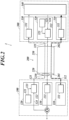
FIG. 2 is a block diagram of a power over fiber system according to a second embodiment of the present disclosure; -
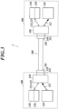
FIG. 3 is a block diagram of the power over fiber system according to the second embodiment of the present disclosure and shows optical connectors and so forth; and -
FIG. 4 is a block diagram of a power over fiber system according to another embodiment of the present disclosure. - Hereinafter, one or more embodiments of the present disclosure will be described with reference to the drawings. However, the scope of the present invention is not limited to the disclosed embodiments or illustrated examples.
- As shown in
FIG. 1 , a power over fiber (PoF) system 1A (optical power supply system) of this embodiment includes a power sourcing equipment (PSE)device 110, anoptical fiber cable 200A and a powered device (PD) 310. - In the present disclosure, a PSE device converts electric power into optical energy and supplies (sources) the optical energy, and a powered device receives (draws) the supplied optical energy and converts the optical energy into electric power.
- The
PSE device 110 includes asemiconductor laser 111 for power supply. - The
optical fiber cable 200A includes anoptical fiber 250A that forms a transmission path of feed light. - The powered
device 310 includes aphotoelectric conversion element 311. - The
PSE device 110 is connected to a power source, and electrically drives thesemiconductor laser 111 and so forth. - The
semiconductor laser 111 oscillates with the electric power from the power source, thereby outputtingfeed light 112. - The
optical fiber cable 200A has oneend 201A (first end) connectable to thePSE device 110 and theother end 202A (second end) connectable to the powereddevice 310 to transmit thefeed light 112. - The
feed light 112 from thePSE device 110 is input to the oneend 201A of theoptical fiber cable 200A, propagates through theoptical fiber 250A, and is output from theother end 202A of theoptical fiber cable 200A to the powereddevice 310. - The
photoelectric conversion element 311 converts thefeed light 112 transmitted through theoptical fiber cable 200A into electric power. The electric power obtained by the conversion of thefeed light 112 by thephotoelectric conversion element 311 is driving power needed in the powereddevice 310. The powereddevice 310 is capable of outputting, for an external device(s), the electric power obtained by the conversion of thefeed light 112 by thephotoelectric conversion element 311. - Semiconductor materials of semiconductor regions of the
semiconductor laser 111 and thephotoelectric conversion element 311 are semiconductors having a laser wavelength being a short wavelength of 500 nm or less. The semiconductor regions exhibit light-electricity conversion effect. - Semiconductors having a laser wavelength being a short wavelength have a large band gap and a high photoelectric conversion efficiency, and hence improve photoelectric conversion efficiency at the power supplying side (PSE side) and the power receiving side (PD side) in optical power supply, and improve optical power supply efficiency.
- Hence, as the semiconductor materials, laser media having a laser wavelength (base wave) of 200 nm to 500 nm may be used. Examples thereof include diamond, gallium oxide, aluminum nitride and gallium nitride.
- Further, as the semiconductor materials, semiconductors having a band gap of 2.4 eV or greater are used.
- For example, laser media having a band gap of 2.4 eV to 6.2 eV may be used. Examples thereof include diamond, gallium oxide, aluminum nitride and gallium nitride.
- Laser light having a longer wavelength tends to have a higher transmission efficiency, whereas laser light having a shorter wavelength tends to have a higher photoelectric conversion efficiency. Hence, when laser light is transmitted for a long distance, laser media having a laser wavelength (base wave) of greater than 500 nm may be used, whereas when the photoelectric conversion efficiency is given priority, laser media having a laser wavelength (base wave) of less than 200 nm may be used.
- Any of these semiconductor materials may be used in one of the
semiconductor laser 111 and thephotoelectric conversion element 311. This improves the photoelectric conversion efficiency at either the PSE side or the PD side, and improves the optical power supply efficiency. - As shown in
FIG. 2 , a power over fiber (PoF)system 1 of this embodiment includes a power supply system through an optical fiber and an optical communication system therethrough, and includes: a firstdata communication device 100 including a power sourcing equipment (PSE)device 110; anoptical fiber cable 200; and a seconddata communication device 300 including a powered device (PD) 310. - The
PSE device 110 includes asemiconductor laser 111 for power supply. The firstdata communication device 100 includes, in addition to thePSE device 110, atransmitter 120 and areceiver 130 for data communication. The firstdata communication device 100 corresponds to a data terminal equipment (DTE) device, a repeater or the like. Thetransmitter 120 includes asemiconductor laser 121 for signals and amodulator 122. Thereceiver 130 includes aphotodiode 131 for signals. - The
optical fiber cable 200 includes anoptical fiber 250 including: a core 210 that forms a transmission path of signal light; and acladding 220 that is arranged so as to surround the core 210 and forms a transmission path of feed light. - The powered
device 310 includes aphotoelectric conversion element 311. The seconddata communication device 300 includes, in addition to the powereddevice 310, atransmitter 320 and areceiver 330 for data communication, and adata processing unit 340. The seconddata communication device 300 corresponds to a power end station or the like. Thetransmitter 320 includes asemiconductor laser 321 for signals and amodulator 322. Thereceiver 330 includes aphotodiode 331 for signals. Thedata processing unit 340 processes received signals. The seconddata communication device 300 is a node in a communication network. The seconddata communication device 300 may be a node that communicates with another node. - The first
data communication device 100 is connected to a power source, and electrically drives thesemiconductor laser 111, thesemiconductor laser 121, themodulator 122, thephotodiode 131 and so forth. The firstdata communication device 100 is a node in a communication network. The firstdata communication device 100 may be a node that communicates with another node. - The
semiconductor laser 111 oscillates with the electric power from the power source, thereby outputtingfeed light 112. - The
photoelectric conversion element 311 converts thefeed light 112 transmitted through theoptical fiber cable 200 into electric power. The electric power obtained by the conversion of thefeed light 112 by thephotoelectric conversion element 311 is driving power needed in the seconddata communication device 300, for example, driving power for thetransmitter 320, thereceiver 330 and thedata processing unit 340. The seconddata communication device 300 may be capable of outputting, for an external device(s), the electric power obtained by the conversion of thefeed light 112 by thephotoelectric conversion element 311. - The
modulator 122 of thetransmitter 120 modulateslaser light 123 output by thesemiconductor laser 121 to signal light 125 on the basis oftransmission data 124, and outputs thesignal light 125. - The
photodiode 331 of thereceiver 330 demodulates thesignal light 125 transmitted through theoptical fiber cable 200 to an electric signal, and outputs the electric signal to thedata processing unit 340. Thedata processing unit 340 transmits data of the electric signal to a node, and also receives data from the node and outputs the data to themodulator 322 astransmission data 324. - The
modulator 322 of thetransmitter 320 modulateslaser light 323 output by thesemiconductor laser 321 to signal light 325 on the basis of thetransmission data 324, and outputs thesignal light 325. - The
photodiode 131 of thereceiver 130 demodulates thesignal light 325 transmitted through theoptical fiber cable 200 to an electric signal, and outputs the electric signal. Data of the electric signal is transmitted to a node, whereas data from the node is thetransmission data 124. - The
feed light 112 and the signal light 125 from the firstdata communication device 100 are input to one end 201 (first end) of theoptical fiber cable 200, propagate through thecladding 220 and the core 210, respectively, and are output from the other end 202 (second end) of theoptical fiber cable 200 to the seconddata communication device 300. - The signal light 325 from the second
data communication device 300 is input to theother end 202 of theoptical fiber cable 200, propagates through the core 210, and is output from the oneend 201 of theoptical fiber cable 200 to the firstdata communication device 100. - As shown in
FIG. 3 , the firstdata communication device 100 includes a light input/output part 140 and an optical connector 141 attached to the light input/output part 140, and the seconddata communication device 300 includes a light input/output part 350 and an optical connector 351 attached to the light input/output part 350. Anoptical connector 230 provided at the oneend 201 of theoptical fiber cable 200 is connected to the optical connector 141, and an optical connector 240 provided at theother end 202 of theoptical fiber cable 200 is connected to the optical connector 351. The light input/output part 140 guides thefeed light 112 to thecladding 220, guides thesignal light 125 to the core 210, and guides thesignal light 325 to thereceiver 130. The light input/output part 350 guides thefeed light 112 to thepowered device 310, guides thesignal light 125 to thereceiver 330, and guides thesignal light 325 to the core 210. - As described above, the
optical fiber cable 200 has the oneend 201 connectable to the firstdata communication device 100 and theother end 202 connectable to the seconddata communication device 300 to transmit thefeed light 112. In this embodiment, theoptical fiber cable 200 transmits thesignal light 125/325 bidirectionally. - As the semiconductor materials of the semiconductor regions, which exhibit the light-electricity conversion effect, of the
semiconductor laser 111 and thephotoelectric conversion element 311, any of those described in the first embodiment can be used, thereby achieving a high optical power supply efficiency. - Although some embodiments of the present disclosure have been described above, these embodiments are made for purposes of illustration and example only. The present invention can be carried out in various other forms, and each component may be omitted, replaced or modified without departing from the scope of the present invention.
- For example, like an
optical fiber cable 200B of a power overfiber system 1B shown inFIG. 4 , anoptical fiber 260 that transmits signal light and anoptical fiber 270 that transmits feed light may be provided separately. Further, theoptical fiber cable 200B may be composed of a plurality of optical fiber cables. - Although power over fiber systems have been described, the present disclosure is applicable to optical power supply in general.
- In an optical power supply system according to at least one embodiment of the present disclosure, a PSE device includes a semiconductor laser that oscillates with electric power, thereby outputting feed light, and includes a semiconductor region exhibiting the light-electricity conversion effect, wherein a semiconductor material of the semiconductor region is a laser medium having a laser wavelength of 500 nm or less.
- In at least one embodiment, the semiconductor material is the laser medium having a band gap of 2.4 eV or greater.
- In at least one embodiment, the semiconductor material is one selected from diamond, gallium oxide, aluminum nitride and gallium nitride.
- In an optical power supply system according to at least one embodiment of the present disclosure, a powered device includes a photoelectric conversion element that converts feed light into electric power, and includes a semiconductor region exhibiting the light-electricity conversion effect, wherein a semiconductor material of the semiconductor region is a laser medium having a laser wavelength of 500 nm or less.
- In at least one embodiment, the semiconductor material is the laser medium having a band gap of 2.4 eV or greater.
- In at least one embodiment, the semiconductor material is one selected from diamond, gallium oxide, aluminum nitride and gallium nitride.
- According to an optical power supply system according to at least one embodiment of the present disclosure, a semiconductor material(s) having a high photoelectric conversion efficiency improves the photoelectric conversion efficiency at the power supplying side (PSE side) and/or the power receiving side (PD side) in optical power supply, and improves the optical power supply efficiency.
- In the following, further embodiments of the present disclosure are described.
- According to a first further embodiment there is provided a power sourcing equipment (PSE) device of an optical power supply system, comprising a semiconductor laser that oscillates with electric power, thereby outputting feed light, and includes a semiconductor region exhibiting a light-electricity conversion effect, wherein a semiconductor material of the semiconductor region is a laser medium having a laser wavelength of 500 nm or less.
- In the first further embodiment the semiconductor material may be the laser medium having a band gap of 2.4 eV or greater.
- In the first further embodiment the semiconductor material may be diamond.
- In the first further embodiment the semiconductor material may be gallium oxide.
- In the first further embodiment the semiconductor material may be aluminum nitride.
- In the first further embodiment the semiconductor material may be gallium nitride.
- According to a second further embodiment there is provided a powered device of an optical power supply system, comprising a photoelectric conversion element that converts feed light into electric power, and includes a semiconductor region exhibiting a light-electricity conversion effect, wherein a semiconductor material of the semiconductor region is a laser medium having a laser wavelength of 500 nm or less.
- In the second further embodiment the semiconductor material may be the laser medium having a band gap of 2.4 eV or greater.
- In the second further embodiment the semiconductor material may be diamond.
- In the second further embodiment the semiconductor material may be gallium oxide.
- In the second further embodiment the semiconductor material may be aluminum nitride.
- In the second further embodiment the semiconductor material may be gallium nitride.
- According to a third further embodiment there is provided an optical power supply system comprising: the PSE device according to the first further embodiment; and a powered device including a photoelectric conversion element that converts the feed light output by the PSE device into electric power.
- According to a fourth further embodiment there is provided an optical power supply system comprising: a power sourcing equipment (PSE) device including a semiconductor laser that oscillates with electric power, thereby outputting feed light; and the powered device according to the second further embodiment, wherein the feed light is input to the powered device.
- In the third or fourth further embodiments the optical power supply system may comprise: a first data communication device including the PSE device; and a second data communication device including the powered device, wherein the first data communication device and the second data communication device perform optical communication with one another, and wherein the electric power obtained by the conversion of the feed light by the photoelectric conversion element is driving power for a transmitter and a receiver included in the second data communication device.
- In the third or fourth further embodiments the optical power supply system may further comprise an optical fiber cable that includes a first end connectable to the PSE device and a second end connectable to the powered device to transmit the feed light.
- In the third or fourth further embodiments the optical power supply system may further comprise an optical fiber cable that includes a first end connectable to the first data communication device and a second end connectable to the second data communication device to transmit the feed light and signal light.
Claims (15)
- A device (100) for an optical power supply system (1A, 1, 1B), comprisinga semiconductor laser (111) configured to output a first light (112) for feeding and including a semiconductor region exhibiting a light-electricity conversion effect, anda first optical fiber cable (200A, 200, 270),characterized in thata semiconductor material of the semiconductor region is a laser medium having a laser wavelength of 500 nm or less, andthe first optical fiber cable (200A, 200, 200B) has a first path configured for the first light to pass through.
- The device (100) according to claim 1, comprisinga first transmitter (120) configured to output a second light for communication, whereinthe first optical fiber cable (200A, 200, 270) has a second path configured for the second light to pass through.
- The device (100) according to claim 2, wherein,
within the first optical fiber cable, the second path is located near a central axis of the first optical fiber cable and the first path is located outside the second path. - The device (100) according to claim 1, comprisinga second optical fiber cable (260), anda first transmitter (120) configured to output a second light for communication, wherein the second optical fiber cable (200B) has a second path configured for the second light to pass through.
- The device (100) according to any one of claims 1 to 4, wherein the laser medium has a laser wavelength of 200 nm to 500nm.
- The device (100) according to any one of claims 1 to 5, wherein the semiconductor material is the laser medium having a band gap of 2.4 eV or greater.
- The device (100) according to any one of claims 1 to 5, wherein the semiconductor material is diamond, or gallium oxide, or aluminum nitride, or gallium nitride.
- An optical power supply system (1A, 1, 1B) comprising:the device according to any one of claims 1 to 7; anda powered device (310) including a photoelectric conversion element (311) configured to convert the first light into electric power.
- The optical power supply system (1A, 1, 1B) according to claim 8, wherein the first optical fiber cable (200A, 200, 200B) is configured to guide the first light from the semiconductor laser (111) towards the photoelectric conversion element (311).
- An optical power supply system (1A, 1, 1B) comprising:the device according to any one of claims 2 to 7;a powered device (310) including a photoelectric conversion element (311) configured to convert the first light into electric power; anda first receiver (330) configured to receive the second light,wherein optionally the optical power supply system (1A, 1, 1B) further comprises a first data processing unit (340), wherein the first receiver (330) is configured to output a first electric signal based on the first light, and wherein the first data processing unit (340) is configured to input the first electric signal from the first receiver (330), andwherein further optionally the first data processing unit (340) is configured to be powered by the powered device (310) .
- An optical power supply system (1A, 1, 1B) comprising:the device according to any one of claims 1 to 3;a powered device (310) including a photoelectric conversion element (311) configured to convert the first light into electric power; anda second transmitter (320) configured to output a third light for communication, wherein the first optical fiber cable (200A, 200, 270) has a third path configured for the third light to pass through.
- An optical power supply system (1A, 1, 1B) comprising:the device according to claim 4;a powered device (310) including a photoelectric conversion element (311) configured to convert the first light into electric power; anda second transmitter (320) configured to output a third light for communication, whereinthe second optical fiber cable (200B) has a third path configured for the third light to pass through.
- The optical power supply system (1A, 1, 1B) according to claim 11 or 12, wherein
the device includes a second receiver (130) configured toreceive the third light andoutput a second electric signal based on the third light. - The optical power supply system (1A, 1, 1B) according to any one of claims 8 to 13, wherein the powered device (310) is configured to output the electric power to at least one of external devices.
- The optical power supply system (1A, 1, 1B) according to any one of claims 11 to 13, wherein the second transmitter (320) is configured to be driven by the electric power.
Applications Claiming Priority (2)
| Application Number | Priority Date | Filing Date | Title |
|---|---|---|---|
| JP2019097548A JP2020194992A (en) | 2019-05-24 | 2019-05-24 | Power supply device and power receiving device of optical power supply system and optical power supply system |
| EP20171783.2A EP3742631B1 (en) | 2019-05-24 | 2020-04-28 | Pse device and powered device of optical power supply system, and optical power supply system |
Related Parent Applications (2)
| Application Number | Title | Priority Date | Filing Date |
|---|---|---|---|
| EP20171783.2A Division EP3742631B1 (en) | 2019-05-24 | 2020-04-28 | Pse device and powered device of optical power supply system, and optical power supply system |
| EP20171783.2A Division-Into EP3742631B1 (en) | 2019-05-24 | 2020-04-28 | Pse device and powered device of optical power supply system, and optical power supply system |
Publications (3)
| Publication Number | Publication Date |
|---|---|
| EP4149023A2 true EP4149023A2 (en) | 2023-03-15 |
| EP4149023A3 EP4149023A3 (en) | 2023-03-22 |
| EP4149023B1 EP4149023B1 (en) | 2025-07-09 |
Family
ID=70475999
Family Applications (3)
| Application Number | Title | Priority Date | Filing Date |
|---|---|---|---|
| EP20171783.2A Active EP3742631B1 (en) | 2019-05-24 | 2020-04-28 | Pse device and powered device of optical power supply system, and optical power supply system |
| EP22205049.4A Active EP4149023B1 (en) | 2019-05-24 | 2020-04-28 | Pse device and powered device of optical power supply system, and optical power supply system |
| EP22161832.5A Active EP4033678B1 (en) | 2019-05-24 | 2020-04-28 | Optical power supply system |
Family Applications Before (1)
| Application Number | Title | Priority Date | Filing Date |
|---|---|---|---|
| EP20171783.2A Active EP3742631B1 (en) | 2019-05-24 | 2020-04-28 | Pse device and powered device of optical power supply system, and optical power supply system |
Family Applications After (1)
| Application Number | Title | Priority Date | Filing Date |
|---|---|---|---|
| EP22161832.5A Active EP4033678B1 (en) | 2019-05-24 | 2020-04-28 | Optical power supply system |
Country Status (4)
| Country | Link |
|---|---|
| US (4) | US11296479B2 (en) |
| EP (3) | EP3742631B1 (en) |
| JP (2) | JP2020194992A (en) |
| CN (1) | CN111988088A (en) |
Families Citing this family (4)
| Publication number | Priority date | Publication date | Assignee | Title |
|---|---|---|---|---|
| JP2020194992A (en) * | 2019-05-24 | 2020-12-03 | 京セラ株式会社 | Power supply device and power receiving device of optical power supply system and optical power supply system |
| US11575055B2 (en) | 2019-07-15 | 2023-02-07 | SLT Technologies, Inc | Methods for coupling of optical fibers to a power photodiode |
| US11398870B2 (en) * | 2020-03-13 | 2022-07-26 | General Electric Company | Systems and methods for optical data communication using wide bandgap semiconductor detectors |
| JP7060638B2 (en) * | 2020-03-16 | 2022-04-26 | 京セラ株式会社 | Power receiving device of optical power supply system and optical power supply system |
Citations (1)
| Publication number | Priority date | Publication date | Assignee | Title |
|---|---|---|---|---|
| JP2010135989A (en) | 2008-12-03 | 2010-06-17 | Mitsubishi Electric Corp | Optic fiber, optical communication device, and optical communication method |
Family Cites Families (17)
| Publication number | Priority date | Publication date | Assignee | Title |
|---|---|---|---|---|
| JP3822318B2 (en) * | 1997-07-17 | 2006-09-20 | 株式会社東芝 | Semiconductor light emitting device and manufacturing method thereof |
| US6493125B1 (en) * | 1998-02-25 | 2002-12-10 | Oki Electric Industry Co., Ltd. | Apparatus for stabilizing light source frequency |
| US20030026310A1 (en) * | 2001-08-06 | 2003-02-06 | Motorola, Inc. | Structure and method for fabrication for a lighting device |
| JP4544606B2 (en) * | 2002-05-17 | 2010-09-15 | 株式会社日本政策投資銀行 | Laser system |
| JP2008530809A (en) * | 2005-02-17 | 2008-08-07 | コーニンクレッカ フィリップス エレクトロニクス エヌ ヴィ | All solid state UV laser system |
| US8609984B2 (en) * | 2009-06-24 | 2013-12-17 | Florida State University Research Foundation, Inc. | High efficiency photovoltaic cell for solar energy harvesting |
| JP2011142544A (en) * | 2010-01-08 | 2011-07-21 | Anritsu Corp | Optical feeding light source and optical feeding rof system using the same |
| JP2012089578A (en) * | 2010-10-15 | 2012-05-10 | Sanyo Electric Co Ltd | Method for manufacturing semiconductor laser device, semiconductor laser device and optical device having the laser device |
| WO2013021606A1 (en) * | 2011-08-09 | 2013-02-14 | パナソニック株式会社 | Structure for growth of nitride semiconductor layer, stacked structure, nitride-based semiconductor element, light source, and manufacturing method for same |
| CN104768454B (en) * | 2012-11-08 | 2018-04-24 | 皇家飞利浦有限公司 | Optical probe system |
| CN104184044A (en) * | 2014-08-20 | 2014-12-03 | 中国科学院西安光学精密机械研究所 | High-power semiconductor laser system and preparation method thereof |
| US9899550B2 (en) * | 2015-08-12 | 2018-02-20 | Toyota Motor Engineering & Manufacturing North America, Inc. | Electric power transfer system using optical power transfer |
| US20170093501A1 (en) * | 2015-09-29 | 2017-03-30 | Semprius, Inc. | Miniaturized devices for combined optical power conversion and data transmission |
| EP3507921B1 (en) * | 2016-09-02 | 2021-07-14 | Koninklijke Philips N.V. | Optical transceiver, optical system, interventional device and method for supplying energy and returning data |
| CN206618914U (en) * | 2017-02-21 | 2017-11-07 | 扬州太光芯片科技有限公司 | Electrooptic modulator based on niobic acid lithium material |
| US11217964B2 (en) * | 2018-12-28 | 2022-01-04 | Intel Corporation | Current channel for III-V silicon hybrid laser |
| JP2020194992A (en) * | 2019-05-24 | 2020-12-03 | 京セラ株式会社 | Power supply device and power receiving device of optical power supply system and optical power supply system |
-
2019
- 2019-05-24 JP JP2019097548A patent/JP2020194992A/en active Pending
-
2020
- 2020-04-28 EP EP20171783.2A patent/EP3742631B1/en active Active
- 2020-04-28 EP EP22205049.4A patent/EP4149023B1/en active Active
- 2020-04-28 EP EP22161832.5A patent/EP4033678B1/en active Active
- 2020-05-07 CN CN202010379863.XA patent/CN111988088A/en active Pending
- 2020-05-08 US US16/870,826 patent/US11296479B2/en active Active
- 2020-07-30 US US16/944,068 patent/US11276981B2/en active Active
-
2022
- 2022-02-03 US US17/591,600 patent/US11757246B2/en active Active
- 2022-02-03 US US17/591,601 patent/US11870204B2/en active Active
-
2023
- 2023-07-25 JP JP2023120369A patent/JP2023153145A/en active Pending
Patent Citations (1)
| Publication number | Priority date | Publication date | Assignee | Title |
|---|---|---|---|---|
| JP2010135989A (en) | 2008-12-03 | 2010-06-17 | Mitsubishi Electric Corp | Optic fiber, optical communication device, and optical communication method |
Also Published As
| Publication number | Publication date |
|---|---|
| EP4033678B1 (en) | 2023-11-08 |
| US11870204B2 (en) | 2024-01-09 |
| EP4149023A3 (en) | 2023-03-22 |
| JP2020194992A (en) | 2020-12-03 |
| US20220158403A1 (en) | 2022-05-19 |
| JP2023153145A (en) | 2023-10-17 |
| US11276981B2 (en) | 2022-03-15 |
| EP4149023B1 (en) | 2025-07-09 |
| US11757246B2 (en) | 2023-09-12 |
| CN111988088A (en) | 2020-11-24 |
| US11296479B2 (en) | 2022-04-05 |
| EP3742631A1 (en) | 2020-11-25 |
| EP3742631B1 (en) | 2023-01-04 |
| EP4033678A1 (en) | 2022-07-27 |
| US20200373724A1 (en) | 2020-11-26 |
| US20200373723A1 (en) | 2020-11-26 |
| US20220158404A1 (en) | 2022-05-19 |
Similar Documents
| Publication | Publication Date | Title |
|---|---|---|
| US11870204B2 (en) | PSE device and powered device of optical power supply system, and optical power supply system | |
| US11323186B2 (en) | Power over fiber system and optical fiber cable | |
| US12250087B2 (en) | Power-over-fiber system | |
| US11362740B2 (en) | Power over fiber system | |
| JP7598985B2 (en) | Photoelectric Adapter | |
| US11888329B2 (en) | Power over fiber system and feed light visualization lid member | |
| US11381320B2 (en) | Optical transmission system | |
| EP3926858B1 (en) | Optical fiber power feeding system | |
| US11888534B2 (en) | Power sourcing equipment of power-over-fiber system and power-over-fiber system |
Legal Events
| Date | Code | Title | Description |
|---|---|---|---|
| PUAI | Public reference made under article 153(3) epc to a published international application that has entered the european phase |
Free format text: ORIGINAL CODE: 0009012 |
|
| STAA | Information on the status of an ep patent application or granted ep patent |
Free format text: STATUS: THE APPLICATION HAS BEEN PUBLISHED |
|
| PUAL | Search report despatched |
Free format text: ORIGINAL CODE: 0009013 |
|
| AC | Divisional application: reference to earlier application |
Ref document number: 3742631 Country of ref document: EP Kind code of ref document: P |
|
| AK | Designated contracting states |
Kind code of ref document: A2 Designated state(s): AL AT BE BG CH CY CZ DE DK EE ES FI FR GB GR HR HU IE IS IT LI LT LU LV MC MK MT NL NO PL PT RO RS SE SI SK SM TR |
|
| AK | Designated contracting states |
Kind code of ref document: A3 Designated state(s): AL AT BE BG CH CY CZ DE DK EE ES FI FR GB GR HR HU IE IS IT LI LT LU LV MC MK MT NL NO PL PT RO RS SE SI SK SM TR |
|
| RIC1 | Information provided on ipc code assigned before grant |
Ipc: H01L 31/028 20060101ALI20230215BHEP Ipc: H01L 31/032 20060101ALI20230215BHEP Ipc: H01L 31/0304 20060101ALI20230215BHEP Ipc: H04B 10/80 20130101AFI20230215BHEP |
|
| P01 | Opt-out of the competence of the unified patent court (upc) registered |
Effective date: 20230505 |
|
| STAA | Information on the status of an ep patent application or granted ep patent |
Free format text: STATUS: REQUEST FOR EXAMINATION WAS MADE |
|
| 17P | Request for examination filed |
Effective date: 20230725 |
|
| RBV | Designated contracting states (corrected) |
Designated state(s): AL AT BE BG CH CY CZ DE DK EE ES FI FR GB GR HR HU IE IS IT LI LT LU LV MC MK MT NL NO PL PT RO RS SE SI SK SM TR |
|
| STAA | Information on the status of an ep patent application or granted ep patent |
Free format text: STATUS: EXAMINATION IS IN PROGRESS |
|
| 17Q | First examination report despatched |
Effective date: 20231012 |
|
| GRAP | Despatch of communication of intention to grant a patent |
Free format text: ORIGINAL CODE: EPIDOSNIGR1 |
|
| STAA | Information on the status of an ep patent application or granted ep patent |
Free format text: STATUS: GRANT OF PATENT IS INTENDED |
|
| RIC1 | Information provided on ipc code assigned before grant |
Ipc: H10F 77/12 20250101ALI20250114BHEP Ipc: H10F 77/122 20250101ALI20250114BHEP Ipc: H10F 77/124 20250101ALI20250114BHEP Ipc: H04B 10/80 20130101AFI20250114BHEP |
|
| INTG | Intention to grant announced |
Effective date: 20250206 |
|
| GRAS | Grant fee paid |
Free format text: ORIGINAL CODE: EPIDOSNIGR3 |
|
| GRAA | (expected) grant |
Free format text: ORIGINAL CODE: 0009210 |
|
| STAA | Information on the status of an ep patent application or granted ep patent |
Free format text: STATUS: THE PATENT HAS BEEN GRANTED |
|
| AC | Divisional application: reference to earlier application |
Ref document number: 3742631 Country of ref document: EP Kind code of ref document: P |
|
| AK | Designated contracting states |
Kind code of ref document: B1 Designated state(s): AL AT BE BG CH CY CZ DE DK EE ES FI FR GB GR HR HU IE IS IT LI LT LU LV MC MK MT NL NO PL PT RO RS SE SI SK SM TR |
|
| REG | Reference to a national code |
Ref country code: GB Ref legal event code: FG4D |
|
| REG | Reference to a national code |
Ref country code: CH Ref legal event code: EP |
|
| REG | Reference to a national code |
Ref country code: IE Ref legal event code: FG4D |
|
| REG | Reference to a national code |
Ref country code: DE Ref legal event code: R096 Ref document number: 602020054445 Country of ref document: DE |
|
| REG | Reference to a national code |
Ref country code: NL Ref legal event code: MP Effective date: 20250709 |
|
| PG25 | Lapsed in a contracting state [announced via postgrant information from national office to epo] |
Ref country code: PT Free format text: LAPSE BECAUSE OF FAILURE TO SUBMIT A TRANSLATION OF THE DESCRIPTION OR TO PAY THE FEE WITHIN THE PRESCRIBED TIME-LIMIT Effective date: 20251110 |
|
| PG25 | Lapsed in a contracting state [announced via postgrant information from national office to epo] |
Ref country code: NL Free format text: LAPSE BECAUSE OF FAILURE TO SUBMIT A TRANSLATION OF THE DESCRIPTION OR TO PAY THE FEE WITHIN THE PRESCRIBED TIME-LIMIT Effective date: 20250709 |
|
| REG | Reference to a national code |
Ref country code: AT Ref legal event code: MK05 Ref document number: 1812865 Country of ref document: AT Kind code of ref document: T Effective date: 20250709 |
|
| PG25 | Lapsed in a contracting state [announced via postgrant information from national office to epo] |
Ref country code: IS Free format text: LAPSE BECAUSE OF FAILURE TO SUBMIT A TRANSLATION OF THE DESCRIPTION OR TO PAY THE FEE WITHIN THE PRESCRIBED TIME-LIMIT Effective date: 20251109 |
|
| PG25 | Lapsed in a contracting state [announced via postgrant information from national office to epo] |
Ref country code: NO Free format text: LAPSE BECAUSE OF FAILURE TO SUBMIT A TRANSLATION OF THE DESCRIPTION OR TO PAY THE FEE WITHIN THE PRESCRIBED TIME-LIMIT Effective date: 20251009 |
|
| REG | Reference to a national code |
Ref country code: LT Ref legal event code: MG9D |
|
| PG25 | Lapsed in a contracting state [announced via postgrant information from national office to epo] |
Ref country code: AT Free format text: LAPSE BECAUSE OF FAILURE TO SUBMIT A TRANSLATION OF THE DESCRIPTION OR TO PAY THE FEE WITHIN THE PRESCRIBED TIME-LIMIT Effective date: 20250709 |
|
| PG25 | Lapsed in a contracting state [announced via postgrant information from national office to epo] |
Ref country code: FI Free format text: LAPSE BECAUSE OF FAILURE TO SUBMIT A TRANSLATION OF THE DESCRIPTION OR TO PAY THE FEE WITHIN THE PRESCRIBED TIME-LIMIT Effective date: 20250709 |
|
| PG25 | Lapsed in a contracting state [announced via postgrant information from national office to epo] |
Ref country code: HR Free format text: LAPSE BECAUSE OF FAILURE TO SUBMIT A TRANSLATION OF THE DESCRIPTION OR TO PAY THE FEE WITHIN THE PRESCRIBED TIME-LIMIT Effective date: 20250709 |
|
| PG25 | Lapsed in a contracting state [announced via postgrant information from national office to epo] |
Ref country code: GR Free format text: LAPSE BECAUSE OF FAILURE TO SUBMIT A TRANSLATION OF THE DESCRIPTION OR TO PAY THE FEE WITHIN THE PRESCRIBED TIME-LIMIT Effective date: 20251010 |
|
| PG25 | Lapsed in a contracting state [announced via postgrant information from national office to epo] |
Ref country code: SE Free format text: LAPSE BECAUSE OF FAILURE TO SUBMIT A TRANSLATION OF THE DESCRIPTION OR TO PAY THE FEE WITHIN THE PRESCRIBED TIME-LIMIT Effective date: 20250709 |
|
| PG25 | Lapsed in a contracting state [announced via postgrant information from national office to epo] |
Ref country code: LV Free format text: LAPSE BECAUSE OF FAILURE TO SUBMIT A TRANSLATION OF THE DESCRIPTION OR TO PAY THE FEE WITHIN THE PRESCRIBED TIME-LIMIT Effective date: 20250709 |
|
| PG25 | Lapsed in a contracting state [announced via postgrant information from national office to epo] |
Ref country code: PL Free format text: LAPSE BECAUSE OF FAILURE TO SUBMIT A TRANSLATION OF THE DESCRIPTION OR TO PAY THE FEE WITHIN THE PRESCRIBED TIME-LIMIT Effective date: 20250709 Ref country code: BG Free format text: LAPSE BECAUSE OF FAILURE TO SUBMIT A TRANSLATION OF THE DESCRIPTION OR TO PAY THE FEE WITHIN THE PRESCRIBED TIME-LIMIT Effective date: 20250709 |
|
| PG25 | Lapsed in a contracting state [announced via postgrant information from national office to epo] |
Ref country code: RS Free format text: LAPSE BECAUSE OF FAILURE TO SUBMIT A TRANSLATION OF THE DESCRIPTION OR TO PAY THE FEE WITHIN THE PRESCRIBED TIME-LIMIT Effective date: 20251009 |
|
| PG25 | Lapsed in a contracting state [announced via postgrant information from national office to epo] |
Ref country code: ES Free format text: LAPSE BECAUSE OF FAILURE TO SUBMIT A TRANSLATION OF THE DESCRIPTION OR TO PAY THE FEE WITHIN THE PRESCRIBED TIME-LIMIT Effective date: 20250709 |
|
| PG25 | Lapsed in a contracting state [announced via postgrant information from national office to epo] |
Ref country code: SM Free format text: LAPSE BECAUSE OF FAILURE TO SUBMIT A TRANSLATION OF THE DESCRIPTION OR TO PAY THE FEE WITHIN THE PRESCRIBED TIME-LIMIT Effective date: 20250709 |
|
| PG25 | Lapsed in a contracting state [announced via postgrant information from national office to epo] |
Ref country code: DK Free format text: LAPSE BECAUSE OF FAILURE TO SUBMIT A TRANSLATION OF THE DESCRIPTION OR TO PAY THE FEE WITHIN THE PRESCRIBED TIME-LIMIT Effective date: 20250709 |
|
| PG25 | Lapsed in a contracting state [announced via postgrant information from national office to epo] |
Ref country code: IT Free format text: LAPSE BECAUSE OF FAILURE TO SUBMIT A TRANSLATION OF THE DESCRIPTION OR TO PAY THE FEE WITHIN THE PRESCRIBED TIME-LIMIT Effective date: 20250709 |
|
| PG25 | Lapsed in a contracting state [announced via postgrant information from national office to epo] |
Ref country code: CZ Free format text: LAPSE BECAUSE OF FAILURE TO SUBMIT A TRANSLATION OF THE DESCRIPTION OR TO PAY THE FEE WITHIN THE PRESCRIBED TIME-LIMIT Effective date: 20250709 |
|
| PG25 | Lapsed in a contracting state [announced via postgrant information from national office to epo] |
Ref country code: EE Free format text: LAPSE BECAUSE OF FAILURE TO SUBMIT A TRANSLATION OF THE DESCRIPTION OR TO PAY THE FEE WITHIN THE PRESCRIBED TIME-LIMIT Effective date: 20250709 Ref country code: SK Free format text: LAPSE BECAUSE OF FAILURE TO SUBMIT A TRANSLATION OF THE DESCRIPTION OR TO PAY THE FEE WITHIN THE PRESCRIBED TIME-LIMIT Effective date: 20250709 |