EP4148795A1 - Flexible display panel and manufacturing method therefor - Google Patents
Flexible display panel and manufacturing method therefor Download PDFInfo
- Publication number
- EP4148795A1 EP4148795A1 EP20917294.9A EP20917294A EP4148795A1 EP 4148795 A1 EP4148795 A1 EP 4148795A1 EP 20917294 A EP20917294 A EP 20917294A EP 4148795 A1 EP4148795 A1 EP 4148795A1
- Authority
- EP
- European Patent Office
- Prior art keywords
- layer
- source
- trace
- drain metal
- display panel
- Prior art date
- Legal status (The legal status is an assumption and is not a legal conclusion. Google has not performed a legal analysis and makes no representation as to the accuracy of the status listed.)
- Pending
Links
- 238000004519 manufacturing process Methods 0.000 title claims abstract description 18
- 229910052751 metal Inorganic materials 0.000 claims abstract description 108
- 239000002184 metal Substances 0.000 claims abstract description 108
- 238000011049 filling Methods 0.000 claims abstract description 74
- 238000005452 bending Methods 0.000 claims abstract description 60
- 239000000758 substrate Substances 0.000 claims abstract description 45
- 239000010410 layer Substances 0.000 claims description 441
- 239000011229 interlayer Substances 0.000 claims description 37
- 230000004888 barrier function Effects 0.000 claims description 17
- 238000000059 patterning Methods 0.000 claims description 7
- 229910003460 diamond Inorganic materials 0.000 claims description 6
- 239000010432 diamond Substances 0.000 claims description 6
- 229910052581 Si3N4 Inorganic materials 0.000 claims description 4
- VYPSYNLAJGMNEJ-UHFFFAOYSA-N Silicium dioxide Chemical compound O=[Si]=O VYPSYNLAJGMNEJ-UHFFFAOYSA-N 0.000 claims description 4
- HQVNEWCFYHHQES-UHFFFAOYSA-N silicon nitride Chemical compound N12[Si]34N5[Si]62N3[Si]51N64 HQVNEWCFYHHQES-UHFFFAOYSA-N 0.000 claims description 4
- 229910052814 silicon oxide Inorganic materials 0.000 claims description 4
- 239000004642 Polyimide Substances 0.000 claims description 2
- 229920001721 polyimide Polymers 0.000 claims description 2
- 230000008859 change Effects 0.000 abstract description 9
- 238000005229 chemical vapour deposition Methods 0.000 description 4
- RYGMFSIKBFXOCR-UHFFFAOYSA-N Copper Chemical compound [Cu] RYGMFSIKBFXOCR-UHFFFAOYSA-N 0.000 description 3
- ZOKXTWBITQBERF-UHFFFAOYSA-N Molybdenum Chemical compound [Mo] ZOKXTWBITQBERF-UHFFFAOYSA-N 0.000 description 3
- 229910052802 copper Inorganic materials 0.000 description 3
- 239000010949 copper Substances 0.000 description 3
- 229910052750 molybdenum Inorganic materials 0.000 description 3
- 239000011733 molybdenum Substances 0.000 description 3
- 230000003287 optical effect Effects 0.000 description 3
- 238000004544 sputter deposition Methods 0.000 description 3
- 229910045601 alloy Inorganic materials 0.000 description 2
- 239000000956 alloy Substances 0.000 description 2
- QVGXLLKOCUKJST-UHFFFAOYSA-N atomic oxygen Chemical compound [O] QVGXLLKOCUKJST-UHFFFAOYSA-N 0.000 description 2
- 238000005516 engineering process Methods 0.000 description 2
- 238000005530 etching Methods 0.000 description 2
- 239000000463 material Substances 0.000 description 2
- 150000002739 metals Chemical class 0.000 description 2
- 238000000034 method Methods 0.000 description 2
- 238000012986 modification Methods 0.000 description 2
- 230000004048 modification Effects 0.000 description 2
- 229910052760 oxygen Inorganic materials 0.000 description 2
- 239000001301 oxygen Substances 0.000 description 2
- 239000004065 semiconductor Substances 0.000 description 2
- 125000006850 spacer group Chemical group 0.000 description 2
- 239000004952 Polyamide Substances 0.000 description 1
- 229910021417 amorphous silicon Inorganic materials 0.000 description 1
- 230000003139 buffering effect Effects 0.000 description 1
- 239000011248 coating agent Substances 0.000 description 1
- 238000000576 coating method Methods 0.000 description 1
- 238000002425 crystallisation Methods 0.000 description 1
- 230000008025 crystallization Effects 0.000 description 1
- 238000010586 diagram Methods 0.000 description 1
- 230000001788 irregular Effects 0.000 description 1
- 238000005224 laser annealing Methods 0.000 description 1
- 239000011368 organic material Substances 0.000 description 1
- 230000000149 penetrating effect Effects 0.000 description 1
- 229920002647 polyamide Polymers 0.000 description 1
- 229910021420 polycrystalline silicon Inorganic materials 0.000 description 1
- 229920005591 polysilicon Polymers 0.000 description 1
- 230000008569 process Effects 0.000 description 1
Images






Classifications
-
- H—ELECTRICITY
- H10—SEMICONDUCTOR DEVICES; ELECTRIC SOLID-STATE DEVICES NOT OTHERWISE PROVIDED FOR
- H10K—ORGANIC ELECTRIC SOLID-STATE DEVICES
- H10K59/00—Integrated devices, or assemblies of multiple devices, comprising at least one organic light-emitting element covered by group H10K50/00
- H10K59/10—OLED displays
- H10K59/17—Passive-matrix OLED displays
- H10K59/179—Interconnections, e.g. wiring lines or terminals
- H10K59/1795—Interconnections, e.g. wiring lines or terminals comprising structures specially adapted for lowering the resistance
-
- H—ELECTRICITY
- H10—SEMICONDUCTOR DEVICES; ELECTRIC SOLID-STATE DEVICES NOT OTHERWISE PROVIDED FOR
- H10K—ORGANIC ELECTRIC SOLID-STATE DEVICES
- H10K59/00—Integrated devices, or assemblies of multiple devices, comprising at least one organic light-emitting element covered by group H10K50/00
- H10K59/10—OLED displays
- H10K59/12—Active-matrix OLED [AMOLED] displays
- H10K59/124—Insulating layers formed between TFT elements and OLED elements
-
- G—PHYSICS
- G09—EDUCATION; CRYPTOGRAPHY; DISPLAY; ADVERTISING; SEALS
- G09F—DISPLAYING; ADVERTISING; SIGNS; LABELS OR NAME-PLATES; SEALS
- G09F9/00—Indicating arrangements for variable information in which the information is built-up on a support by selection or combination of individual elements
- G09F9/30—Indicating arrangements for variable information in which the information is built-up on a support by selection or combination of individual elements in which the desired character or characters are formed by combining individual elements
- G09F9/301—Indicating arrangements for variable information in which the information is built-up on a support by selection or combination of individual elements in which the desired character or characters are formed by combining individual elements flexible foldable or roll-able electronic displays, e.g. thin LCD, OLED
-
- H—ELECTRICITY
- H10—SEMICONDUCTOR DEVICES; ELECTRIC SOLID-STATE DEVICES NOT OTHERWISE PROVIDED FOR
- H10K—ORGANIC ELECTRIC SOLID-STATE DEVICES
- H10K59/00—Integrated devices, or assemblies of multiple devices, comprising at least one organic light-emitting element covered by group H10K50/00
- H10K59/10—OLED displays
- H10K59/12—Active-matrix OLED [AMOLED] displays
- H10K59/131—Interconnections, e.g. wiring lines or terminals
- H10K59/1315—Interconnections, e.g. wiring lines or terminals comprising structures specially adapted for lowering the resistance
-
- H—ELECTRICITY
- H10—SEMICONDUCTOR DEVICES; ELECTRIC SOLID-STATE DEVICES NOT OTHERWISE PROVIDED FOR
- H10K—ORGANIC ELECTRIC SOLID-STATE DEVICES
- H10K59/00—Integrated devices, or assemblies of multiple devices, comprising at least one organic light-emitting element covered by group H10K50/00
- H10K59/80—Constructional details
- H10K59/805—Electrodes
- H10K59/8051—Anodes
- H10K59/80516—Anodes combined with auxiliary electrodes, e.g. ITO layer combined with metal lines
-
- H—ELECTRICITY
- H10—SEMICONDUCTOR DEVICES; ELECTRIC SOLID-STATE DEVICES NOT OTHERWISE PROVIDED FOR
- H10K—ORGANIC ELECTRIC SOLID-STATE DEVICES
- H10K77/00—Constructional details of devices covered by this subclass and not covered by groups H10K10/80, H10K30/80, H10K50/80 or H10K59/80
- H10K77/10—Substrates, e.g. flexible substrates
- H10K77/111—Flexible substrates
-
- H—ELECTRICITY
- H10—SEMICONDUCTOR DEVICES; ELECTRIC SOLID-STATE DEVICES NOT OTHERWISE PROVIDED FOR
- H10K—ORGANIC ELECTRIC SOLID-STATE DEVICES
- H10K2102/00—Constructional details relating to the organic devices covered by this subclass
- H10K2102/301—Details of OLEDs
- H10K2102/311—Flexible OLED
-
- H—ELECTRICITY
- H10—SEMICONDUCTOR DEVICES; ELECTRIC SOLID-STATE DEVICES NOT OTHERWISE PROVIDED FOR
- H10K—ORGANIC ELECTRIC SOLID-STATE DEVICES
- H10K59/00—Integrated devices, or assemblies of multiple devices, comprising at least one organic light-emitting element covered by group H10K50/00
- H10K59/10—OLED displays
- H10K59/12—Active-matrix OLED [AMOLED] displays
- H10K59/1201—Manufacture or treatment
-
- H—ELECTRICITY
- H10—SEMICONDUCTOR DEVICES; ELECTRIC SOLID-STATE DEVICES NOT OTHERWISE PROVIDED FOR
- H10K—ORGANIC ELECTRIC SOLID-STATE DEVICES
- H10K71/00—Manufacture or treatment specially adapted for the organic devices covered by this subclass
-
- H—ELECTRICITY
- H10—SEMICONDUCTOR DEVICES; ELECTRIC SOLID-STATE DEVICES NOT OTHERWISE PROVIDED FOR
- H10K—ORGANIC ELECTRIC SOLID-STATE DEVICES
- H10K71/00—Manufacture or treatment specially adapted for the organic devices covered by this subclass
- H10K71/20—Changing the shape of the active layer in the devices, e.g. patterning
-
- Y—GENERAL TAGGING OF NEW TECHNOLOGICAL DEVELOPMENTS; GENERAL TAGGING OF CROSS-SECTIONAL TECHNOLOGIES SPANNING OVER SEVERAL SECTIONS OF THE IPC; TECHNICAL SUBJECTS COVERED BY FORMER USPC CROSS-REFERENCE ART COLLECTIONS [XRACs] AND DIGESTS
- Y02—TECHNOLOGIES OR APPLICATIONS FOR MITIGATION OR ADAPTATION AGAINST CLIMATE CHANGE
- Y02E—REDUCTION OF GREENHOUSE GAS [GHG] EMISSIONS, RELATED TO ENERGY GENERATION, TRANSMISSION OR DISTRIBUTION
- Y02E10/00—Energy generation through renewable energy sources
- Y02E10/50—Photovoltaic [PV] energy
- Y02E10/549—Organic PV cells
Definitions
- the present invention relates to a field of display technology and in particular, to a flexible display panel and a manufacturing method thereof.
- OLED organic light-emitting diode
- the flexible and foldable display needs to be rolled or bent during use, and even frequently bent. As the number of bending increases, it is easy to cause the resistance of traces in the source/drain metal layer to increase, which leads to lower brightness of the display and broken traces in source/drain metal layer, thus causing poor display performance.
- the present invention provides a flexible display panel and a manufacturing method thereof to solve the problem that with a continuous increase in the number of bending of a conventional flexible display panel, resistance of traces in a source/drain metal layer tends to increase, resulting in a decrease in brightness and broken traces in the source/drain metal layer.
- the present invention provides a technical solution as follows:
- the present invention provides a flexible display panel, comprising a bending region and a non-bending region, the flexible display panel comprising:
- the inorganic layer comprises:
- the organic filling layer is provided with at least one groove structure arranged in an area corresponding to the bending region and disposed on one side away from the base substrate, and the first source/drain metal layer trace forms the curved trace through the at least one groove structure.
- the groove structure penetrates the organic filling layer, and the first source/drain metal layer trace is arranged among the interlayer dielectric layer, the organic filling layer, and the planarization layer.
- an aperture diameter of the groove structure ranges from 2um to 20um.
- a cross-sectional shape of the groove structure comprises a trapezoid, a rectangle, a square, a circle, a diamond, or a triangle.
- the flexible display panel further comprises a second via hole defined in the bending region, and the second via hole is extended through the interlayer dielectric layer, the second insulating layer, the first insulating layer, and the buffer layer, and the organic filling layer is filled in the second via hole.
- the present invention provides a flexible display panel which comprises a bending region and a non-bending region, the flexible display panel comprising:
- the inorganic layer comprises:
- the organic filling layer is provided with at least one groove structure arranged in an area corresponding to the bending region and disposed on one side away from the base substrate, and the first source/drain metal layer trace forms a curved trace through the groove structure.
- a bottom portion of the groove structure is in contact with the organic filling layer, and the first source/drain metal layer trace is arranged between the organic filling layer and the planarization layer.
- the groove structure penetrates the organic filling layer, and the first source/drain metal layer trace is arranged among the interlayer dielectric layer, the organic filling layer, and the planarization layer.
- an aperture diameter of the groove structure ranges from 2um to 20um.
- a depth of the groove structure ranges from 0.5um to 1.5um.
- a cross-sectional shape of the groove structure comprises a trapezoid, a rectangle, a square, a circle, a diamond, or a triangle.
- the flexible display panel further comprises a second via hole defined in the bending region, the second via hole is extended through the interlayer dielectric layer, the second insulating layer, the first insulating layer, and the buffer layer, and the organic filling layer is filled in the second via hole.
- the buffer layer is made of silicon nitride or silicon oxide.
- the present invention provides a manufacturing method of a flexible display panel, comprising following steps:
- step S20 comprises following steps:
- the source/drain metal layer trace is a curved trace, so that when the flexible display panel is bent, the source/drain metal layer trace is subjected to alternate compressive stress and tensile stress, and the compressive stress and tensile stress can neutralize each other. Accordingly, the stress is reduced, thereby reducing a resistance change of the source/drain metal layer trace caused by bending, and further reducing an optical change caused by the resistance change.
- the present invention can reduce a risk of breakage of the source/drain metal layer trace and improve product performance of the flexible display panel.
- the present invention solves a problem with a conventional flexible display panel.
- the problem is that, as the number of bending increases, resistance of traces of a source/drain metal layer tends to increase, resulting in a decrease in brightness and breakage of the traces of the source/drain metal layer.
- the present invention can solve this problem.
- a flexible display panel 1 is provided according to one embodiment of the present invention.
- the flexible display panel 1 includes a display region.
- An integrated chip and a flexible circuit board are arranged at an edge of the display region.
- the display region comprises a bending region 1a and a non-bending region 1b.
- the bending region 1a refers to an area that needs to be bent or folded.
- the non-bending region 1b refers to an area that does not need to be bent or folded.
- the bending region 1a and the non-bending region 1b both can be used to display images.
- the bending region 1a can be arranged at any position of the display region. In consideration of user habits, the bending region 1a of the present embodiment is arranged in the middle of the display region, and the flexible display panel 1 can be bent or folded along a bending axis of the bending region 1a.
- the flexible display panel 1 comprises an array substrate, and the array substrate comprises a base substrate 10.
- the base substrate 10 is a flexible substrate, which can be made of a polyamide material.
- an inorganic layer 20 is arranged on the base substrate 10. It should be noted that the inorganic layer 20 comprises, but is not limited to, a moisture barrier layer (an oxygen and moisture barrier layer) 201, a buffer layer 202, an active layer 203, a first insulating layer 204, a first gate layer trace 205, a second insulating layer 206, a second gate layer trace 207, and an interlayer dielectric layer 208.
- a moisture barrier layer an oxygen and moisture barrier layer
- the inorganic layer 20 comprises: the moisture barrier layer 201 arranged on the base substrate 10, wherein the moisture barrier layer 201 is configured to prevent external moisture or oxygen from corroding a device layer of the flexible display panel 1; the buffer layer 202 arranged on the moisture barrier layer 201, wherein the buffer layer 202 can be made of silicon nitride or silicon oxide for buffering and protection; the active layer 203 arranged on the buffer layer 202, wherein the active layer 203 can be made of polysilicon or amorphous silicon, and the active layer 203 comprises a semiconductor region 2031 arranged in the middle and doped regions 2032 arranged at two ends of the semiconductor region 2031; the first insulating layer 204 covering the buffer layer 202 and the active layer 203; the first gate layer trace 205 arranged on the first insulating layer 204; the second insulating layer 206 covering the first insulating layer 204 and the first gate layer trace 205; the second gate layer trace 207 arranged on the second insulating layer 206;
- first gate layer trace 205 and the second gate layer trace 207 can be made of metals or alloys containing molybdenum, copper, and etc.
- the first insulating layer 204, the second insulating layer 206, and the interlayer dielectric layer 208 can be made of silicon oxide, silicon nitride, or other materials.
- An organic filling layer 30 is arranged on the inorganic layer 20, and the organic filling layer 30 can be made of a flexible organic material such as PI.
- Source/drain metal layer traces are arranged on the organic filling layer 40.
- the source/drain metal layer trace includes a first source/drain metal layer trace 401 located in the bending region 1a and a second source/drain metal layer trace 402 located in the non-bending region 1b.
- the source/drain metal layer trace can be made of metals or alloys containing molybdenum, copper, and etc.
- the source/drain metal layer trace is connected to the doped region 2032 of the active layer 203 through a first via hole 901 extended through the first insulating layer 204, the second insulating layer 206, and the interlayer dielectric layer 208.
- the organic filling layer 30 is arranged between the source/drain metal layer trace and the interlayer dielectric layer 208.
- the first source/drain metal layer trace 401 tends to break. At the same time, as the number of bending increases, it is easy to cause the resistance of the first source/drain metal layer trace 401 to increase, resulting in a decrease in the brightness.
- the first source/drain metal layer trace 401 located in the bending region 1a is designed as a curved trace, so that the first source/drain metal layer trace 401 receives alternate compressive stress and tensile stress, and the compressive stress and the tensile stress can neutralize each other, which effectively reduces a risk of trace breakage, and at the same time, reduces an optical change caused by the resistance change of the first source/drain metal layer trace 401 to improve product performance.
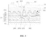
- the organic filling layer 30 is provided with at least one groove structure 301 arranged in an area corresponding to the bending region 1a and disposed on one side away from the base substrate 10, and the first source/drain metal layer trace 401 forms the curved trace through the groove structure 301.
- the groove structure 301 does not completely penetrate the organic filling layer 30, and a bottom of the groove structure 301 is in contact with the organic filling layer 30.
- the first source/drain metal layer trace 401 is disposed between the organic filling layer 30 and the planarization layer 50.
- the planarization layer 50 is arranged on the source/drain metal layer trace.
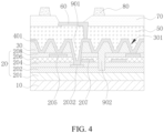
- the groove structure 301 completely penetrates the organic filling layer 30, and the first source/drain metal layer trace 401 is arranged among the interlayer dielectric layer 208, the organic filling layer 30, and the planarization layer 50.
- the groove structure 301 includes crests and troughs.
- the first source/drain metal layer trace 401 is subjected to tensile stress at the crests of the groove structure 301 and compressive stress at the troughs of the groove structure 301, so the tensile stress and the compressive stress at the crests and the troughs can neutralize each other.
- the tensile stress and the compressive stress of the first source/drain metal layer trace 401 at the crests and troughs can neutralize each other.
- the first source/drain metal layer trace 401 is subjected to compressive stress at the crests of the groove structure 301 and tensile stress at the troughs of the groove structure 301. Therefore, the compressive stress and the tensile stress at the crests and the troughs can neutralize each other, thereby reducing overall stress on the first source/drain metal layer trace 401.
- a thickness of the organic filling layer 30 is 1.5um
- an aperture diameter of the groove structure 301 ranges from 2um to 20um
- a depth of the groove structure 301 ranges from 0.5um to 1.5um. It should be noted that the thickness of the organic filling layer 30, the aperture diameter of the groove structure 301, and the depth of the groove structure 301 can be designed according to actual conditions of the flexible display panel 1.
- a cross-sectional shape of the groove structure 301 comprises a trapezoid, a rectangle, a square, a circle, a diamond, a triangle, or a special shape.
- the present invention is not intended to limit the cross-sectional shape of the groove structure 301.
- the flexible display panel 1 further comprises a second via hole 902 arranged in the bending region 1a, and the second via hole 902 penetrates the interlayer dielectric layer 208, the second insulating layer 206, the first insulating layer 204, and the buffer layer 202.
- the organic filling layer 30 is filled in the second via hole 902.
- the organic filling layer 30 can adjust stress between the upper and lower film layers in the inorganic layer 20, and can spread the stress of the inorganic layer 20 during bending to thereby prevent breakage of the first source/drain metal layer trace 401.
- the flexible display panel 1 further comprises an anode layer 60 disposed on the planarization layer 50, a pixel definition layer 70, and a spacer layer 80 disposed on the pixel definition layer 70, wherein a light-emitting layer is arranged in an opening area of the pixel definition layer 70.
- a manufacturing method of a flexible display panel 1 is provided according to one embodiment of the present invention.
- the manufacturing method comprises the following steps: As shown in FIG. 6A , step S10: providing a base substrate 10.
- the base substrate 10 is flexible substrate.
- Step S20 forming an inorganic layer 20 on the base substrate 10.
- step S20 comprises the following steps: S201: sequentially forming a moisture barrier layer 201, a buffer layer 202, an active layer 203, a first insulating layer 204, a first gate layer trace 205, a second insulating layer 206, a second gate layer trace 207, and an interlayer dielectric layer 208 on the base substrate 10.
- the moisture barrier layer 201 and the buffer layer 202 can be formed by chemical vapor deposition, and then the active layer 203 can be formed by crystallization, exposure, and etching by performing an excimer laser annealing method.
- the first insulating layer 204 can be formed by chemical vapor deposition.
- a first metal layer is formed by radio frequency sputtering, and exposed and etched to form the first gate layer trace 205.
- the second insulating layer 206 is formed by chemical vapor deposition; a second metal layer is formed by radio frequency sputtering, and exposed and etched to form the second gate layer trace 207.
- the interlayer dielectric layer 208 is formed by chemical vapor deposition.
- Step S202 forming a second via hole 902 extended through the first insulating layer 204, the second insulating layer 206, and the interlayer dielectric layer 208.
- the first insulating layer 204, the second insulating layer 206, and the interlayer dielectric layer 208 are exposed and developed to form the second via hole 902.
- step S30 forming an organic filling layer 30 on the inorganic layer 20, and patterning the organic filling layer 30, so that the organic filling layer 30 forms at least one groove structure 301 in an area corresponding to the bending region 1a and on one side away from the base substrate 10.
- the organic filling layer 30 can be formed on the interlayer dielectric layer 208 by coating, and the organic filling layer 30 can be exposed by using a halftone mask 2.
- the halftone mask 2 comprises a light-transmissive region 100, a semi-transmissive region 200, and a non-transmissive region 300.
- the light-transmissive region 100 is arranged corresponding to an area where the first via hole 901 needs to be formed in the flexible display panel 1
- the semi-transmissive region 200 is arranged corresponding to an area where the groove structure 301 needs to be formed in the flexible display panel 1
- the non-transmissive region 300 is arranged corresponding to the rest area of the flexible display panel 1.
- the halftone mask 2 can be used to make the first via hole 901 and the groove structure 301 at the same time, thus saving manufacturing steps and improving production efficiency.
- another mask with a different structure can be used to prepare the first via hole 901 and the groove structure 301 successively, and a detailed description thereof is not provided here for brevity.
- a thickness of the organic filling layer 30 is 1.5um
- an aperture diameter of the groove structure 301 ranges from 2um to 20um
- a depth of the groove structure 301 ranges from 0.5um to 1.5um
- the groove structure 301 completely penetrates or does not completely penetrate the organic filling layer 30
- a cross-sectional shape of the groove structure 301 is a trapezoid, a rectangle, a square, a circle, a diamond, a triangle, or a special shape (e.g., an irregular hole).
- step S40 forming a source/drain metal layer on the organic filling layer 30, and patterning the source/drain metal layer to form a first source/drain metal layer trace 401 in the bending region 1a and a second source/drain metal layer trace 402 in the non-bending region 1b, wherein the first source/drain metal layer trace 401 forms a curved trace through the groove structure 301.
- the source/drain metal layer trace can be formed by sputtering.
- step S40 patterning the organic filling layer 30 includes exposure, development, etching, and etc., which can also form the first via hole 901 penetrating the first insulating layer 204, the second insulating layer 206, and the interlayer dielectric layer 208, wherein the first via hole 901 is connected to the active layer 203.
- step S50 forming a planarization layer 50 on the source/drain metal layer traces.
- the manufacturing method of the flexible display panel 1 further comprises forming an anode layer 60, a pixel definition layer 70, and a spacer layer 80 on the planarization layer 50, and the anode layer 60 is connected to the source/drain metal layer trace through the via hole.
- the source/drain metal layer trace is designed as a curved trace, so that when the flexible display panel 1 is bent, the source/drain metal layer trace is subjected to alternate compressive stress and tensile stress, and thereby the compressive stress and the tensile stress can neutralize each other to reduce the stress.
- Such a configuration reduces the resistance change of the source/drain metal layer trace caused by bending, thereby reducing the optical change caused by the resistance change.
- the present invention can reduce the risk of breakage of the source/drain metal layer trace, and improve the product performance of the flexible display panel 1.
Landscapes
- Engineering & Computer Science (AREA)
- Microelectronics & Electronic Packaging (AREA)
- Physics & Mathematics (AREA)
- General Physics & Mathematics (AREA)
- Theoretical Computer Science (AREA)
- Electroluminescent Light Sources (AREA)
- Devices For Indicating Variable Information By Combining Individual Elements (AREA)
- Manufacturing & Machinery (AREA)
Abstract
Description
- The present invention relates to a field of display technology and in particular, to a flexible display panel and a manufacturing method thereof.
- In recent years, organic light-emitting diode (OLED) displays have received great attention and been used extensively due to advantages such as a high contrast ratio, wide viewing angles, and flexibility. Especially, the flexibility feature grabs attention from the majority of users. As the technology becomes mature, flexible and foldable displays also appear on the market.
- The flexible and foldable display needs to be rolled or bent during use, and even frequently bent. As the number of bending increases, it is easy to cause the resistance of traces in the source/drain metal layer to increase, which leads to lower brightness of the display and broken traces in source/drain metal layer, thus causing poor display performance.
- In summary, it is necessary to provide a new flexible display panel and a manufacturing method thereof to solve the above technical problems.
- The present invention provides a flexible display panel and a manufacturing method thereof to solve the problem that with a continuous increase in the number of bending of a conventional flexible display panel, resistance of traces in a source/drain metal layer tends to increase, resulting in a decrease in brightness and broken traces in the source/drain metal layer.
- To solve the above problems, the present invention provides a technical solution as follows:
The present invention provides a flexible display panel, comprising a bending region and a non-bending region, the flexible display panel comprising: - a base substrate;
- an inorganic layer arranged on the base substrate;
- an organic filling layer arranged on the inorganic layer, wherein the organic filling layer is made of polyimide;
- source/drain metal layer traces disposed on the organic filling layer, wherein the source/drain metal layer traces comprise a first source/drain metal layer trace arranged in the bending region and a second source/drain metal layer trace arranged in the non-bending region, and the first source/drain metal layer trace is a curved trace; and
- a planarization layer arranged at one side of the source/drain metal layer traces away from the base substrate.
- In the flexible display panel according to one embodiment of the present invention, the inorganic layer comprises:
- a moisture barrier layer arranged on the base substrate;
- a buffer layer arranged on the moisture barrier layer;
- an active layer arranged on the buffer layer;
- a first insulating layer covering the buffer layer and the active layer;
- a first gate layer trace arranged on the first insulating layer;
- a second insulating layer covering the first insulating layer and the first gate layer trace;
- a second gate layer trace arranged on the second insulating layer; and an interlayer dielectric layer covering the second insulating layer and the second gate layer trace;
- wherein the source/drain layer traces are disposed on the organic filling layer, the source/drain metal layer traces are connected to the active layer through a first via hole extended through the first insulating layer, the second insulating layer, and the interlayer dielectric layer, and the organic filling layer is arranged between the source/drain metal layer traces and the interlayer dielectric layer.
- In the flexible display panel according to one embodiment of the present invention, the organic filling layer is provided with at least one groove structure arranged in an area corresponding to the bending region and disposed on one side away from the base substrate, and the first source/drain metal layer trace forms the curved trace through the at least one groove structure.
- In the flexible display panel according to one embodiment of the present invention, wherein a bottom portion of the groove structure is in contact with the organic filling layer, and the first source/drain metal layer trace is arranged between the organic filling layer and the planarization layer.
- In the flexible display panel according to one embodiment of the present invention, the groove structure penetrates the organic filling layer, and the first source/drain metal layer trace is arranged among the interlayer dielectric layer, the organic filling layer, and the planarization layer.
- In the flexible display panel according to one embodiment of the present invention, an aperture diameter of the groove structure ranges from 2um to 20um.
- In the flexible display panel according to one embodiment of the present invention, a cross-sectional shape of the groove structure comprises a trapezoid, a rectangle, a square, a circle, a diamond, or a triangle.
- In the flexible display panel according to one embodiment of the present invention, the flexible display panel further comprises a second via hole defined in the bending region, and the second via hole is extended through the interlayer dielectric layer, the second insulating layer, the first insulating layer, and the buffer layer, and the organic filling layer is filled in the second via hole.
- The present invention provides a flexible display panel which comprises a bending region and a non-bending region, the flexible display panel comprising:
- a base substrate
- an inorganic layer arranged on the base substrate;
- an organic filling layer arranged on the inorganic layer;
- source/drain metal layer traces disposed on the organic filling layer, the source/drain metal layer traces comprising a first source/drain metal layer trace arranged in the bending region and a second source/drain metal layer trace arranged in the non-bending region; and
- a planarization layer arranged at one side of the source/drain metal layer away from the base substrate.
- In the flexible display panel according to one embodiment of the present invention, the inorganic layer comprises:
- a moisture barrier layer arranged on the base substrate;
- a buffer layer arranged on the moisture barrier layer;
- an active layer arranged on the buffer layer;
- a first insulating layer covering the buffer layer and the active layer;
- a first gate layer trace arranged on the first insulating layer;
- a second insulating layer covering the first insulating layer and the first gate layer trace;
- a second gate layer trace arranged on the second insulating layer; and
- an interlayer dielectric layer covering the second insulating layer and the second gate layer trace;
- wherein the source/drain layer traces are disposed on the organic filling layer, the source/drain metal layer traces are connected to the active layer through a first via hole extended through the first insulating layer, the second insulating layer, and the interlayer dielectric layer, and the organic filling layer is arranged between the source/drain metal layer traces and the interlayer dielectric layer.
- In the flexible display panel according to one embodiment of the present invention, the organic filling layer is provided with at least one groove structure arranged in an area corresponding to the bending region and disposed on one side away from the base substrate, and the first source/drain metal layer trace forms a curved trace through the groove structure.
- In the flexible display panel according to one embodiment of the present invention, a bottom portion of the groove structure is in contact with the organic filling layer, and the first source/drain metal layer trace is arranged between the organic filling layer and the planarization layer.
- In the flexible display panel according to one embodiment of the present invention, the groove structure penetrates the organic filling layer, and the first source/drain metal layer trace is arranged among the interlayer dielectric layer, the organic filling layer, and the planarization layer.
- In the flexible display panel according to one embodiment of the present invention, an aperture diameter of the groove structure ranges from 2um to 20um.
- In the flexible display panel according to one embodiment of the present invention, a depth of the groove structure ranges from 0.5um to 1.5um.
- In the flexible display panel according to one embodiment of the present invention, a cross-sectional shape of the groove structure comprises a trapezoid, a rectangle, a square, a circle, a diamond, or a triangle.
- In the flexible display panel according to one embodiment of the present invention, the flexible display panel further comprises a second via hole defined in the bending region, the second via hole is extended through the interlayer dielectric layer, the second insulating layer, the first insulating layer, and the buffer layer, and the organic filling layer is filled in the second via hole.
- In the flexible display panel according to one embodiment of the present invention, the buffer layer is made of silicon nitride or silicon oxide.
- The present invention provides a manufacturing method of a flexible display panel, comprising following steps:
- S10: providing a base substrate;
- S20: forming an inorganic layer on the base substrate;
- S30: forming an organic filling layer on the inorganic layer, and patterning the organic filling layer, so that the organic filling layer forms at least one groove structure arranged in an area corresponding to the bending region and disposed on one side away from the base substrate;
- S40: forming source/drain metal layer traces on the organic filling layer, and patterning the source/drain metal layer to form a first source/drain metal layer trace in the bending region and a second source/drain metal layer trace in the non-bending region, wherein the first source/drain metal layer trace forms a curved trace through the groove structure; and
- S50: forming a planarization layer on the source/drain metal layer trace.
- In the manufacturing method of the flexible display panel, step S20 comprises following steps:
- S201: sequentially forming a moisture barrier layer, a buffer layer, an active layer, a first insulating layer, a first gate layer trace, a second insulating layer, a second gate layer trace, and an interlayer dielectric layer on the base substrate; and
- S202: forming a second via hole extended through the first insulating layer, the second insulating layer, and the interlayer dielectric layer.
- In the flexible display panel and the manufacturing method thereof provided by the present invention, the source/drain metal layer trace is a curved trace, so that when the flexible display panel is bent, the source/drain metal layer trace is subjected to alternate compressive stress and tensile stress, and the compressive stress and tensile stress can neutralize each other. Accordingly, the stress is reduced, thereby reducing a resistance change of the source/drain metal layer trace caused by bending, and further reducing an optical change caused by the resistance change. At the same time, the present invention can reduce a risk of breakage of the source/drain metal layer trace and improve product performance of the flexible display panel.
- In order to more clearly illustrate the embodiments of the present disclosure or related art, figures which will be described in the embodiments are briefly introduced hereinafter. It is obvious that the drawings are merely for the purposes of illustrating some embodiments of the present disclosure, and a person having ordinary skill in this field can obtain other figures according to these figures without inventive work.
-
FIG. 1 is a schematic plan view illustrating a structure of a flexible display panel according to one embodiment of the present invention; -
FIG. 2 is a schematic cross-sectional view, taken along line A-A, illustrating the flexible display panel according to one embodiment of the present invention; -
FIG. 3 is a schematic cross-sectional view, taken along line B-B, illustrating a flexible display panel according to one embodiment of the present invention; -
FIG. 4 is a schematic cross-sectional view, taken along line B-B, illustrating the flexible display panel according to one embodiment of the present invention; -
FIG. 5 is a process flow diagram illustrating a manufacturing method of the flexible display panel according to one embodiment of the present invention; and -
FIGs. 6A to 6G are schematic views illustrating the manufacturing method of the flexible display panel according to one embodiment of the present invention. - A description is provided below with reference to the accompanying drawings to illustrate specific embodiments of the present invention. The directional terms mentioned in the present invention, such as "upper", "lower", "front", "rear", "left", "right", "inner", "outer", and "lateral", are for illustrative purposes based on the accompanying drawings. Therefore, the directional terms are only used to describe and understand the present invention, rather than to limit the present invention. In the drawings, structurally similar elements are indicated by the same reference numerals.
- The present invention solves a problem with a conventional flexible display panel. The problem is that, as the number of bending increases, resistance of traces of a source/drain metal layer tends to increase, resulting in a decrease in brightness and breakage of the traces of the source/drain metal layer. The present invention can solve this problem.
- As shown in
FIG. 1 , aflexible display panel 1 is provided according to one embodiment of the present invention. Theflexible display panel 1 includes a display region. An integrated chip and a flexible circuit board are arranged at an edge of the display region. The display region comprises a bending region 1a and anon-bending region 1b. The bending region 1a refers to an area that needs to be bent or folded. Thenon-bending region 1b refers to an area that does not need to be bent or folded. The bending region 1a and thenon-bending region 1b both can be used to display images. The bending region 1a can be arranged at any position of the display region. In consideration of user habits, the bending region 1a of the present embodiment is arranged in the middle of the display region, and theflexible display panel 1 can be bent or folded along a bending axis of the bending region 1a. - As shown in
FIGs. 2 and3 , structurally, theflexible display panel 1 comprises an array substrate, and the array substrate comprises abase substrate 10. Thebase substrate 10 is a flexible substrate, which can be made of a polyamide material. - An
inorganic layer 20 is arranged on thebase substrate 10. It should be noted that theinorganic layer 20 comprises, but is not limited to, a moisture barrier layer (an oxygen and moisture barrier layer) 201, abuffer layer 202, anactive layer 203, a first insulatinglayer 204, a firstgate layer trace 205, a second insulatinglayer 206, a secondgate layer trace 207, and aninterlayer dielectric layer 208. In the present embodiment, theinorganic layer 20 comprises: themoisture barrier layer 201 arranged on thebase substrate 10, wherein themoisture barrier layer 201 is configured to prevent external moisture or oxygen from corroding a device layer of theflexible display panel 1; thebuffer layer 202 arranged on themoisture barrier layer 201, wherein thebuffer layer 202 can be made of silicon nitride or silicon oxide for buffering and protection; theactive layer 203 arranged on thebuffer layer 202, wherein theactive layer 203 can be made of polysilicon or amorphous silicon, and theactive layer 203 comprises asemiconductor region 2031 arranged in the middle anddoped regions 2032 arranged at two ends of thesemiconductor region 2031; the first insulatinglayer 204 covering thebuffer layer 202 and theactive layer 203; the firstgate layer trace 205 arranged on the first insulatinglayer 204; the second insulatinglayer 206 covering the first insulatinglayer 204 and the firstgate layer trace 205; the secondgate layer trace 207 arranged on the second insulatinglayer 206; and theinterlayer dielectric layer 208 covering the second insulatinglayer 206 and the secondgate layer trace 207. - In detail, the first
gate layer trace 205 and the secondgate layer trace 207 can be made of metals or alloys containing molybdenum, copper, and etc. The first insulatinglayer 204, the second insulatinglayer 206, and theinterlayer dielectric layer 208 can be made of silicon oxide, silicon nitride, or other materials. - An
organic filling layer 30 is arranged on theinorganic layer 20, and theorganic filling layer 30 can be made of a flexible organic material such as PI. Source/drain metal layer traces are arranged on theorganic filling layer 40. The source/drain metal layer trace includes a first source/drainmetal layer trace 401 located in the bending region 1a and a second source/drain metal layer trace 402 located in thenon-bending region 1b. The source/drain metal layer trace can be made of metals or alloys containing molybdenum, copper, and etc. The source/drain metal layer trace is connected to the dopedregion 2032 of theactive layer 203 through a first viahole 901 extended through the first insulatinglayer 204, the second insulatinglayer 206, and theinterlayer dielectric layer 208. Theorganic filling layer 30 is arranged between the source/drain metal layer trace and theinterlayer dielectric layer 208. - Because molybdenum and copper have lower hardness, when the
flexible display panel 1 is bent, the first source/drainmetal layer trace 401 tends to break. At the same time, as the number of bending increases, it is easy to cause the resistance of the first source/drainmetal layer trace 401 to increase, resulting in a decrease in the brightness. Therefore, the first source/drainmetal layer trace 401 located in the bending region 1a is designed as a curved trace, so that the first source/drainmetal layer trace 401 receives alternate compressive stress and tensile stress, and the compressive stress and the tensile stress can neutralize each other, which effectively reduces a risk of trace breakage, and at the same time, reduces an optical change caused by the resistance change of the first source/drainmetal layer trace 401 to improve product performance. - Furthermore, in the present embodiment, the
organic filling layer 30 is provided with at least onegroove structure 301 arranged in an area corresponding to the bending region 1a and disposed on one side away from thebase substrate 10, and the first source/drainmetal layer trace 401 forms the curved trace through thegroove structure 301. - In one embodiment, as shown in
FIG. 3 , thegroove structure 301 does not completely penetrate theorganic filling layer 30, and a bottom of thegroove structure 301 is in contact with theorganic filling layer 30. The first source/drainmetal layer trace 401 is disposed between theorganic filling layer 30 and theplanarization layer 50. Theplanarization layer 50 is arranged on the source/drain metal layer trace. - Preferably, in another embodiment, as shown in
FIG. 4 , thegroove structure 301 completely penetrates theorganic filling layer 30, and the first source/drainmetal layer trace 401 is arranged among theinterlayer dielectric layer 208, theorganic filling layer 30, and theplanarization layer 50. - The
groove structure 301 includes crests and troughs. When theflexible display panel 1 is folded inward (bent to one side close to the base substrate 10), the first source/drainmetal layer trace 401 is subjected to tensile stress at the crests of thegroove structure 301 and compressive stress at the troughs of thegroove structure 301, so the tensile stress and the compressive stress at the crests and the troughs can neutralize each other. Similarly, the tensile stress and the compressive stress of the first source/drainmetal layer trace 401 at the crests and troughs can neutralize each other. When theflexible display panel 1 is folded outward (bent toward one side away from the base substrate 10), the first source/drainmetal layer trace 401 is subjected to compressive stress at the crests of thegroove structure 301 and tensile stress at the troughs of thegroove structure 301. Therefore, the compressive stress and the tensile stress at the crests and the troughs can neutralize each other, thereby reducing overall stress on the first source/drainmetal layer trace 401. - Specifically, when the
flexible display panel 1 is bent, positions of the bending region 1a are subjected to uniform stress, so thegroove structures 30 are evenly spaced in a direction perpendicular to the axis of the bending region 1a. In one embodiment of the present invention, a thickness of theorganic filling layer 30 is 1.5um, an aperture diameter of thegroove structure 301 ranges from 2um to 20um, and a depth of thegroove structure 301 ranges from 0.5um to 1.5um. It should be noted that the thickness of theorganic filling layer 30, the aperture diameter of thegroove structure 301, and the depth of thegroove structure 301 can be designed according to actual conditions of theflexible display panel 1. - In detail, a cross-sectional shape of the
groove structure 301 comprises a trapezoid, a rectangle, a square, a circle, a diamond, a triangle, or a special shape. However, the present invention is not intended to limit the cross-sectional shape of thegroove structure 301. - Furthermore, the
flexible display panel 1 further comprises a second viahole 902 arranged in the bending region 1a, and the second viahole 902 penetrates theinterlayer dielectric layer 208, the second insulatinglayer 206, the first insulatinglayer 204, and thebuffer layer 202. Theorganic filling layer 30 is filled in the second viahole 902. Theorganic filling layer 30 can adjust stress between the upper and lower film layers in theinorganic layer 20, and can spread the stress of theinorganic layer 20 during bending to thereby prevent breakage of the first source/drainmetal layer trace 401. - The
flexible display panel 1 further comprises ananode layer 60 disposed on theplanarization layer 50, apixel definition layer 70, and aspacer layer 80 disposed on thepixel definition layer 70, wherein a light-emitting layer is arranged in an opening area of thepixel definition layer 70. - As shown in
FIG. 5 , a manufacturing method of aflexible display panel 1 is provided according to one embodiment of the present invention. The manufacturing method comprises the following steps:
As shown inFIG. 6A , step S10: providing abase substrate 10. - The
base substrate 10 is flexible substrate. - Step S20: forming an
inorganic layer 20 on thebase substrate 10. - Referring to
FIG. 6B , step S20 comprises the following steps:
S201: sequentially forming amoisture barrier layer 201, abuffer layer 202, anactive layer 203, a first insulatinglayer 204, a firstgate layer trace 205, a second insulatinglayer 206, a secondgate layer trace 207, and aninterlayer dielectric layer 208 on thebase substrate 10. - First, the
moisture barrier layer 201 and thebuffer layer 202 can be formed by chemical vapor deposition, and then theactive layer 203 can be formed by crystallization, exposure, and etching by performing an excimer laser annealing method. Next, the first insulatinglayer 204 can be formed by chemical vapor deposition. After that, a first metal layer is formed by radio frequency sputtering, and exposed and etched to form the firstgate layer trace 205. Afterwards, the second insulatinglayer 206 is formed by chemical vapor deposition; a second metal layer is formed by radio frequency sputtering, and exposed and etched to form the secondgate layer trace 207. Finally, theinterlayer dielectric layer 208 is formed by chemical vapor deposition. - Step S202: forming a second via
hole 902 extended through the first insulatinglayer 204, the second insulatinglayer 206, and theinterlayer dielectric layer 208. - The first insulating
layer 204, the second insulatinglayer 206, and theinterlayer dielectric layer 208 are exposed and developed to form the second viahole 902. - As shown in
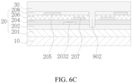
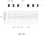
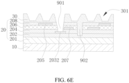
FIGs. 6C ,6D , and6E , step S30: forming anorganic filling layer 30 on theinorganic layer 20, and patterning theorganic filling layer 30, so that theorganic filling layer 30 forms at least onegroove structure 301 in an area corresponding to the bending region 1a and on one side away from thebase substrate 10. - The
organic filling layer 30 can be formed on theinterlayer dielectric layer 208 by coating, and theorganic filling layer 30 can be exposed by using a halftone mask 2. The halftone mask 2 comprises a light-transmissive region 100, asemi-transmissive region 200, and anon-transmissive region 300. The light-transmissive region 100 is arranged corresponding to an area where the first viahole 901 needs to be formed in theflexible display panel 1, thesemi-transmissive region 200 is arranged corresponding to an area where thegroove structure 301 needs to be formed in theflexible display panel 1, and thenon-transmissive region 300 is arranged corresponding to the rest area of theflexible display panel 1. - The halftone mask 2 can be used to make the first via
hole 901 and thegroove structure 301 at the same time, thus saving manufacturing steps and improving production efficiency. Certainly, another mask with a different structure can be used to prepare the first viahole 901 and thegroove structure 301 successively, and a detailed description thereof is not provided here for brevity. - Specifically, a thickness of the
organic filling layer 30 is 1.5um, an aperture diameter of thegroove structure 301 ranges from 2um to 20um, a depth of thegroove structure 301 ranges from 0.5um to 1.5um, and thegroove structure 301 completely penetrates or does not completely penetrate theorganic filling layer 30; a cross-sectional shape of thegroove structure 301 is a trapezoid, a rectangle, a square, a circle, a diamond, a triangle, or a special shape (e.g., an irregular hole). - As shown in
FIG. 6F , step S40: forming a source/drain metal layer on theorganic filling layer 30, and patterning the source/drain metal layer to form a first source/drainmetal layer trace 401 in the bending region 1a and a second source/drain metal layer trace 402 in thenon-bending region 1b, wherein the first source/drainmetal layer trace 401 forms a curved trace through thegroove structure 301. - The source/drain metal layer trace can be formed by sputtering.
- It should be noted that in step S40, patterning the
organic filling layer 30 includes exposure, development, etching, and etc., which can also form the first viahole 901 penetrating the first insulatinglayer 204, the second insulatinglayer 206, and theinterlayer dielectric layer 208, wherein the first viahole 901 is connected to theactive layer 203. - As shown in
FIG. 6G , step S50: forming aplanarization layer 50 on the source/drain metal layer traces. - At the same time, the manufacturing method of the
flexible display panel 1 further comprises forming ananode layer 60, apixel definition layer 70, and aspacer layer 80 on theplanarization layer 50, and theanode layer 60 is connected to the source/drain metal layer trace through the via hole. - Advantages of the present invention: In the
flexible display panel 1 and the manufacturing method thereof provided by the present invention, the source/drain metal layer trace is designed as a curved trace, so that when theflexible display panel 1 is bent, the source/drain metal layer trace is subjected to alternate compressive stress and tensile stress, and thereby the compressive stress and the tensile stress can neutralize each other to reduce the stress. Such a configuration reduces the resistance change of the source/drain metal layer trace caused by bending, thereby reducing the optical change caused by the resistance change. At the same time, the present invention can reduce the risk of breakage of the source/drain metal layer trace, and improve the product performance of theflexible display panel 1. - In summary, although the present invention has been disclosed in preferable embodiments as above, the above-mentioned embodiments are not intended to limit the present invention. Persons of ordinary skill in the art can make various modifications and changes. Such changes and modifications are deemed to be within the protection scope of the present invention defined by the appended claims.
Claims (20)
- A flexible display panel, comprising a bending region and a non-bending region, the flexible display panel comprising:a base substrate;an inorganic layer arranged on the base substrate;an organic filling layer arranged on the inorganic layer, wherein the organic filling layer is made of polyimide;source/drain metal layer traces disposed on the organic filling layer, wherein the source/drain metal layer traces comprise a first source/drain metal layer trace arranged in the bending region and a second source/drain metal layer trace arranged in the non-bending region, and the first source/drain metal layer trace is a curved trace; anda planarization layer arranged at one side of the source/drain metal layer traces away from the base substrate.
- The flexible display panel according to claim 1, wherein the inorganic layer comprises:a moisture barrier layer arranged on the base substrate;a buffer layer arranged on the moisture barrier layer;an active layer arranged on the buffer layer;a first insulating layer covering the buffer layer and the active layer;a first gate layer trace arranged on the first insulating layer;a second insulating layer covering the first insulating layer and the first gate layer trace;a second gate layer trace arranged on the second insulating layer; andan interlayer dielectric layer covering the second insulating layer and the second gate layer trace;wherein the source/drain layer traces are disposed on the organic filling layer, the source/drain metal layer traces are connected to the active layer through a first via hole extended through the first insulating layer, the second insulating layer, and the interlayer dielectric layer, and the organic filling layer is arranged between the source/drain metal layer traces and the interlayer dielectric layer.
- The flexible display panel according to claim 2, wherein the organic filling layer is provided with at least one groove structure arranged in an area corresponding to the bending region and disposed on one side away from the base substrate, and the first source/drain metal layer trace forms the curved trace through the at least one groove structure.
- The flexible display panel according to claim 3, wherein a bottom portion of the groove structure is in contact with the organic filling layer, and the first source/drain metal layer trace is arranged between the organic filling layer and the planarization layer.
- The flexible display panel according to claim 3, wherein the groove structure penetrates the organic filling layer, and the first source/drain metal layer trace is arranged among the interlayer dielectric layer, the organic filling layer, and the planarization layer.
- The flexible display panel according to claim 3, wherein an aperture diameter of the groove structure ranges from 2um to 20um.
- The flexible display panel according to claim 3, wherein a cross-sectional shape of the groove structure comprises a trapezoid, a rectangle, a square, a circle, a diamond, or a triangle.
- The flexible display panel according to claim 2, wherein the flexible display panel further comprises a second via hole defined in the bending region, and the second via hole is extended through the interlayer dielectric layer, the second insulating layer, the first insulating layer, and the buffer layer, and the organic filling layer is filled in the second via hole.
- A flexible display panel, comprising a bending region and a non-bending region, the flexible display panel comprising:a base substratean inorganic layer arranged on the base substrate;an organic filling layer arranged on the inorganic layer;source/drain metal layer traces disposed on the organic filling layer, the source/drain metal layer traces comprising a first source/drain metal layer trace arranged in the bending region and a second source/drain metal layer trace arranged in the non-bending region; anda planarization layer arranged at one side of the source/drain metal layer away from the base substrate.
- The flexible display panel according to claim 9, wherein the inorganic layer comprises:a moisture barrier layer arranged on the base substrate;a buffer layer arranged on the moisture barrier layer;an active layer arranged on the buffer layer;a first insulating layer covering the buffer layer and the active layer;a first gate layer trace arranged on the first insulating layer;a second insulating layer covering the first insulating layer and the first gate layer trace;a second gate layer trace arranged on the second insulating layer; andan interlayer dielectric layer covering the second insulating layer and the second gate layer trace;wherein the source/drain metal layer traces are disposed on the organic filling layer, the source/drain metal layer traces are connected to the active layer through a first via hole extended through the first insulating layer, the second insulating layer, and the interlayer dielectric layer, and the organic filling layer is arranged between the source/drain metal layer traces and the interlayer dielectric layer.
- The flexible display panel according to claim 10, wherein the organic filling layer is provided with at least one groove structure arranged in an area corresponding to the bending region and disposed on one side away from the base substrate, and the first source/drain metal layer trace forms a curved trace through the groove structure.
- The flexible display panel according to claim 11, wherein a bottom portion of the groove structure is in contact with the organic filling layer, and the first source/drain metal layer trace is arranged between the organic filling layer and the planarization layer.
- The flexible display panel according to claim 11, wherein the groove structure penetrates the organic filling layer, and the first source/drain metal layer trace is arranged among the interlayer dielectric layer, the organic filling layer, and the planarization layer.
- The flexible display panel according to claim 11, wherein an aperture diameter of the groove structure ranges from 2um to 20um.
- The flexible display panel according to claim 11, wherein a depth of the groove structure ranges from 0.5um to 1.5um.
- The flexible display panel according to claim 11, wherein a cross-sectional shape of the groove structure comprises a trapezoid, a rectangle, a square, a circle, a diamond, or a triangle.
- The flexible display panel according to claim 10, wherein the flexible display panel further comprises a second via hole defined in the bending region, the second via hole is extended through the interlayer dielectric layer, the second insulating layer, the first insulating layer, and the buffer layer, and the organic filling layer is filled in the second via hole.
- The flexible display panel according to claim 10, wherein the buffer layer is made of silicon nitride or silicon oxide.
- A manufacturing method of a flexible display panel, comprising following steps:S10: providing a base substrate;S20: forming an inorganic layer on the base substrate;S30: forming an organic filling layer on the inorganic layer, and patterning the organic filling layer, so that the organic filling layer forms at least one groove structure arranged in an area corresponding to the bending region and disposed on one side away from the base substrate;S40: forming source/drain metal layer traces on the organic filling layer, and patterning the source/drain metal layer to form a first source/drain metal layer trace in the bending region and a second source/drain metal layer trace in the non-bending region, wherein the first source/drain metal layer trace forms a curved trace through the groove structure; andS50: forming a planarization layer on the source/drain metal layer trace.
- The manufacturing method of the flexible display panel according to claim 19,
wherein step S20 comprises following steps:S201: sequentially forming a moisture barrier layer, a buffer layer, an active layer, a first insulating layer, a first gate layer trace, a second insulating layer, a second gate layer trace, and an interlayer dielectric layer on the base substrate; andS202: forming a second via hole extended through the first insulating layer, the second insulating layer, and the interlayer dielectric layer.
Applications Claiming Priority (2)
| Application Number | Priority Date | Filing Date | Title |
|---|---|---|---|
| CN202010341431.XA CN111415969B (en) | 2020-04-27 | 2020-04-27 | Flexible display panel and manufacturing method thereof |
| PCT/CN2020/097814 WO2021217841A1 (en) | 2020-04-27 | 2020-06-23 | Flexible display panel and manufacturing method therefor |
Publications (2)
| Publication Number | Publication Date |
|---|---|
| EP4148795A1 true EP4148795A1 (en) | 2023-03-15 |
| EP4148795A4 EP4148795A4 (en) | 2024-07-31 |
Family
ID=71494971
Family Applications (1)
| Application Number | Title | Priority Date | Filing Date |
|---|---|---|---|
| EP20917294.9A Pending EP4148795A4 (en) | 2020-04-27 | 2020-06-23 | Flexible display panel and manufacturing method therefor |
Country Status (5)
| Country | Link |
|---|---|
| US (1) | US11758782B2 (en) |
| EP (1) | EP4148795A4 (en) |
| JP (1) | JP2022534635A (en) |
| CN (1) | CN111415969B (en) |
| WO (1) | WO2021217841A1 (en) |
Families Citing this family (12)
| Publication number | Priority date | Publication date | Assignee | Title |
|---|---|---|---|---|
| CN111799280A (en) | 2020-07-20 | 2020-10-20 | 京东方科技集团股份有限公司 | Display substrate and preparation method thereof, and display device |
| CN112002699B (en) * | 2020-08-05 | 2023-04-07 | 武汉华星光电半导体显示技术有限公司 | Flexible display panel and display device |
| CN112802876B (en) * | 2020-11-30 | 2023-04-07 | 京东方科技集团股份有限公司 | Display panel, preparation method thereof and display device |
| CN112951846B (en) * | 2021-01-28 | 2023-04-18 | 京东方科技集团股份有限公司 | Display panel, manufacturing method thereof and display device |
| CN113745247A (en) * | 2021-08-20 | 2021-12-03 | 武汉华星光电半导体显示技术有限公司 | display panel |
| CN114171567B (en) * | 2021-12-07 | 2023-05-05 | 深圳市华星光电半导体显示技术有限公司 | OLED display panel and electronic equipment |
| CN114203734B (en) | 2021-12-11 | 2023-08-22 | 武汉华星光电半导体显示技术有限公司 | Display panel and manufacturing method thereof |
| CN114495722A (en) * | 2022-02-10 | 2022-05-13 | 深圳市华星光电半导体显示技术有限公司 | Display panel |
| CN114530462B (en) * | 2022-02-18 | 2025-04-15 | 京东方科技集团股份有限公司 | Display substrate and preparation method thereof, display panel, and display device |
| CN114743988A (en) * | 2022-04-01 | 2022-07-12 | 云谷(固安)科技有限公司 | Array substrate, manufacturing method thereof and display panel |
| CN115032842B (en) | 2022-07-01 | 2023-11-28 | 武汉华星光电技术有限公司 | Display panel and display terminal |
| CN115346438A (en) * | 2022-08-04 | 2022-11-15 | 武汉华星光电半导体显示技术有限公司 | Flexible display panel |
Family Cites Families (16)
| Publication number | Priority date | Publication date | Assignee | Title |
|---|---|---|---|---|
| KR102405257B1 (en) * | 2015-01-28 | 2022-06-03 | 삼성디스플레이 주식회사 | Display device |
| US10361385B2 (en) * | 2016-02-12 | 2019-07-23 | Samsung Display Co., Ltd. | Display device |
| KR102381286B1 (en) * | 2017-05-18 | 2022-03-31 | 삼성디스플레이 주식회사 | Display device |
| KR102465376B1 (en) * | 2017-06-16 | 2022-11-10 | 삼성디스플레이 주식회사 | Display apparatus and method for manufacturing the same |
| KR102370406B1 (en) * | 2017-07-10 | 2022-03-07 | 삼성디스플레이 주식회사 | Organic light emitting display device and a method of manufacturing organic light emitting display device |
| US10754387B2 (en) | 2017-09-29 | 2020-08-25 | Sharp Kabushiki Kaisha | Flexible display device |
| CN107910335A (en) * | 2017-11-08 | 2018-04-13 | 武汉华星光电半导体显示技术有限公司 | Flexible display panels, flexible display panels production method and display device |
| CN107946317B (en) * | 2017-11-20 | 2020-04-24 | 京东方科技集团股份有限公司 | Flexible array substrate, preparation method, display substrate and display device |
| CN108231800B (en) | 2018-02-02 | 2019-10-29 | 京东方科技集团股份有限公司 | A kind of flexible display panels and preparation method thereof, display device |
| CN108493198B (en) * | 2018-04-11 | 2020-11-24 | 京东方科技集团股份有限公司 | Array substrate and manufacturing method thereof, and organic light emitting diode display device |
| TWI666492B (en) * | 2018-07-09 | 2019-07-21 | 友達光電股份有限公司 | Active device substrate |
| CN109166880A (en) * | 2018-07-25 | 2019-01-08 | 武汉华星光电半导体显示技术有限公司 | Flexible OLED display panel and preparation method thereof |
| US10770667B2 (en) * | 2018-08-21 | 2020-09-08 | Wuhan China Star Optoelectronics Semiconductor Display Technology Co., Ltd. | Flexible display device and manufacturing method thereof |
| CN109300964B (en) * | 2018-10-26 | 2020-10-16 | 武汉华星光电半导体显示技术有限公司 | Flexible OLED panel and manufacturing method thereof |
| US10964731B2 (en) | 2018-12-04 | 2021-03-30 | Wuhan China Star Optoelectronics Semiconductor Display Technology Co., Ltd. | Array substrate and manufacturing method thereof and display device |
| CN109671719A (en) * | 2018-12-04 | 2019-04-23 | 武汉华星光电半导体显示技术有限公司 | Array substrate and preparation method thereof, display device |
-
2020
- 2020-04-27 CN CN202010341431.XA patent/CN111415969B/en active Active
- 2020-06-23 US US17/054,290 patent/US11758782B2/en active Active
- 2020-06-23 WO PCT/CN2020/097814 patent/WO2021217841A1/en not_active Ceased
- 2020-06-23 JP JP2021523496A patent/JP2022534635A/en active Pending
- 2020-06-23 EP EP20917294.9A patent/EP4148795A4/en active Pending
Also Published As
| Publication number | Publication date |
|---|---|
| CN111415969A (en) | 2020-07-14 |
| US11758782B2 (en) | 2023-09-12 |
| US20220157923A1 (en) | 2022-05-19 |
| WO2021217841A1 (en) | 2021-11-04 |
| EP4148795A4 (en) | 2024-07-31 |
| JP2022534635A (en) | 2022-08-03 |
| CN111415969B (en) | 2022-04-08 |
Similar Documents
| Publication | Publication Date | Title |
|---|---|---|
| EP4148795A1 (en) | Flexible display panel and manufacturing method therefor | |
| CN103258743B (en) | Thin-film transistor, thin-film transistor array base-plate and manufacture method thereof | |
| CN100454604C (en) | Flat panel display and manufacturing method thereof | |
| US7586197B2 (en) | Wire structure, method of forming wire, thin film transistor substrate, and method of manufacturing thin film transistor substrate | |
| US7335912B2 (en) | Organic light emitting display having improved via hole | |
| KR100579182B1 (en) | Manufacturing Method of Organic Electroluminescent Display | |
| WO2021022594A1 (en) | Array substrate, display panel, and manufacturing method of array substrate | |
| TWI527118B (en) | Method for manufacturing film and display metal wire thin film transistor array panel using the same and manufacturing method of the same | |
| KR20110009954A (en) | Array substrate and its manufacturing method | |
| US11637159B2 (en) | Display panel and display device with completed covered hollowed regions in frame region | |
| KR20100005303A (en) | Array substrate and method of fabricating the same | |
| KR20130066410A (en) | Method for manufacturing thin film transistor having three-layered metal gate element | |
| CN115020621A (en) | Display panel, preparation method of display panel and display terminal | |
| CN111834546A (en) | Display device, display panel and manufacturing method thereof | |
| CN110112142A (en) | Array substrate and its manufacturing method, display panel and electronic device | |
| KR100635065B1 (en) | Organic EL display device and manufacturing method thereof | |
| EP1724854A1 (en) | Organic electroluminescent device and method for manufacturing the same | |
| KR100543001B1 (en) | Thin Film Transistors and Active Matrix Flat Panel Displays | |
| US7923312B2 (en) | Fabricating method of thin film transistor | |
| KR20130007872A (en) | Array substrate for organic electro luminescent device and method of fabricating the same | |
| KR20050029826A (en) | Fpd and method of fabricating the same | |
| US12193270B2 (en) | Flexible display panel with open pores and flexible array substrate | |
| JP7763599B2 (en) | Display device and manufacturing method thereof | |
| CN114141789B (en) | Display panel | |
| CN1808266B (en) | Photomask and method of manufacturing thin film transistor array panel using same |
Legal Events
| Date | Code | Title | Description |
|---|---|---|---|
| STAA | Information on the status of an ep patent application or granted ep patent |
Free format text: STATUS: UNKNOWN |
|
| STAA | Information on the status of an ep patent application or granted ep patent |
Free format text: STATUS: THE INTERNATIONAL PUBLICATION HAS BEEN MADE |
|
| PUAI | Public reference made under article 153(3) epc to a published international application that has entered the european phase |
Free format text: ORIGINAL CODE: 0009012 |
|
| STAA | Information on the status of an ep patent application or granted ep patent |
Free format text: STATUS: REQUEST FOR EXAMINATION WAS MADE |
|
| 17P | Request for examination filed |
Effective date: 20210813 |
|
| AK | Designated contracting states |
Kind code of ref document: A1 Designated state(s): AL AT BE BG CH CY CZ DE DK EE ES FI FR GB GR HR HU IE IS IT LI LT LU LV MC MK MT NL NO PL PT RO RS SE SI SK SM TR |
|
| DAV | Request for validation of the european patent (deleted) | ||
| DAX | Request for extension of the european patent (deleted) | ||
| REG | Reference to a national code |
Ref country code: DE Ref legal event code: R079 Free format text: PREVIOUS MAIN CLASS: H01L0027120000 Ipc: H01L0021770000 |
|
| A4 | Supplementary search report drawn up and despatched |
Effective date: 20240701 |
|
| RIC1 | Information provided on ipc code assigned before grant |
Ipc: H10K 71/20 20230101ALN20240625BHEP Ipc: H10K 71/00 20230101ALN20240625BHEP Ipc: H10K 59/80 20230101ALI20240625BHEP Ipc: H10K 59/131 20230101ALI20240625BHEP Ipc: H10K 59/124 20230101ALI20240625BHEP Ipc: H01L 21/77 20170101AFI20240625BHEP |