EP4148710A1 - Display substrate, display panel, display apparatus, and manufacturing method for display panel - Google Patents
Display substrate, display panel, display apparatus, and manufacturing method for display panel Download PDFInfo
- Publication number
- EP4148710A1 EP4148710A1 EP20897666.2A EP20897666A EP4148710A1 EP 4148710 A1 EP4148710 A1 EP 4148710A1 EP 20897666 A EP20897666 A EP 20897666A EP 4148710 A1 EP4148710 A1 EP 4148710A1
- Authority
- EP
- European Patent Office
- Prior art keywords
- layer
- display
- display substrate
- groove
- opening
- Prior art date
- Legal status (The legal status is an assumption and is not a legal conclusion. Google has not performed a legal analysis and makes no representation as to the accuracy of the status listed.)
- Pending
Links
Images

Classifications
-
- H—ELECTRICITY
- H10—SEMICONDUCTOR DEVICES; ELECTRIC SOLID-STATE DEVICES NOT OTHERWISE PROVIDED FOR
- H10K—ORGANIC ELECTRIC SOLID-STATE DEVICES
- H10K59/00—Integrated devices, or assemblies of multiple devices, comprising at least one organic light-emitting element covered by group H10K50/00
- H10K59/10—OLED displays
- H10K59/12—Active-matrix OLED [AMOLED] displays
- H10K59/121—Active-matrix OLED [AMOLED] displays characterised by the geometry or disposition of pixel elements
-
- G—PHYSICS
- G09—EDUCATION; CRYPTOGRAPHY; DISPLAY; ADVERTISING; SEALS
- G09F—DISPLAYING; ADVERTISING; SIGNS; LABELS OR NAME-PLATES; SEALS
- G09F9/00—Indicating arrangements for variable information in which the information is built-up on a support by selection or combination of individual elements
- G09F9/30—Indicating arrangements for variable information in which the information is built-up on a support by selection or combination of individual elements in which the desired character or characters are formed by combining individual elements
-
- G—PHYSICS
- G09—EDUCATION; CRYPTOGRAPHY; DISPLAY; ADVERTISING; SEALS
- G09F—DISPLAYING; ADVERTISING; SIGNS; LABELS OR NAME-PLATES; SEALS
- G09F9/00—Indicating arrangements for variable information in which the information is built-up on a support by selection or combination of individual elements
- G09F9/30—Indicating arrangements for variable information in which the information is built-up on a support by selection or combination of individual elements in which the desired character or characters are formed by combining individual elements
- G09F9/302—Indicating arrangements for variable information in which the information is built-up on a support by selection or combination of individual elements in which the desired character or characters are formed by combining individual elements characterised by the form or geometrical disposition of the individual elements
-
- H—ELECTRICITY
- H10—SEMICONDUCTOR DEVICES; ELECTRIC SOLID-STATE DEVICES NOT OTHERWISE PROVIDED FOR
- H10K—ORGANIC ELECTRIC SOLID-STATE DEVICES
- H10K59/00—Integrated devices, or assemblies of multiple devices, comprising at least one organic light-emitting element covered by group H10K50/00
- H10K59/10—OLED displays
- H10K59/12—Active-matrix OLED [AMOLED] displays
- H10K59/1201—Manufacture or treatment
-
- H—ELECTRICITY
- H10—SEMICONDUCTOR DEVICES; ELECTRIC SOLID-STATE DEVICES NOT OTHERWISE PROVIDED FOR
- H10K—ORGANIC ELECTRIC SOLID-STATE DEVICES
- H10K59/00—Integrated devices, or assemblies of multiple devices, comprising at least one organic light-emitting element covered by group H10K50/00
- H10K59/10—OLED displays
- H10K59/12—Active-matrix OLED [AMOLED] displays
- H10K59/122—Pixel-defining structures or layers, e.g. banks
-
- H—ELECTRICITY
- H10—SEMICONDUCTOR DEVICES; ELECTRIC SOLID-STATE DEVICES NOT OTHERWISE PROVIDED FOR
- H10K—ORGANIC ELECTRIC SOLID-STATE DEVICES
- H10K59/00—Integrated devices, or assemblies of multiple devices, comprising at least one organic light-emitting element covered by group H10K50/00
- H10K59/10—OLED displays
- H10K59/12—Active-matrix OLED [AMOLED] displays
- H10K59/123—Connection of the pixel electrodes to the thin film transistors [TFT]
-
- H—ELECTRICITY
- H10—SEMICONDUCTOR DEVICES; ELECTRIC SOLID-STATE DEVICES NOT OTHERWISE PROVIDED FOR
- H10K—ORGANIC ELECTRIC SOLID-STATE DEVICES
- H10K59/00—Integrated devices, or assemblies of multiple devices, comprising at least one organic light-emitting element covered by group H10K50/00
- H10K59/10—OLED displays
- H10K59/12—Active-matrix OLED [AMOLED] displays
- H10K59/124—Insulating layers formed between TFT elements and OLED elements
-
- H—ELECTRICITY
- H10—SEMICONDUCTOR DEVICES; ELECTRIC SOLID-STATE DEVICES NOT OTHERWISE PROVIDED FOR
- H10K—ORGANIC ELECTRIC SOLID-STATE DEVICES
- H10K59/00—Integrated devices, or assemblies of multiple devices, comprising at least one organic light-emitting element covered by group H10K50/00
- H10K59/10—OLED displays
- H10K59/12—Active-matrix OLED [AMOLED] displays
- H10K59/131—Interconnections, e.g. wiring lines or terminals
-
- H—ELECTRICITY
- H10—SEMICONDUCTOR DEVICES; ELECTRIC SOLID-STATE DEVICES NOT OTHERWISE PROVIDED FOR
- H10K—ORGANIC ELECTRIC SOLID-STATE DEVICES
- H10K59/00—Integrated devices, or assemblies of multiple devices, comprising at least one organic light-emitting element covered by group H10K50/00
- H10K59/80—Constructional details
- H10K59/87—Passivation; Containers; Encapsulations
- H10K59/871—Self-supporting sealing arrangements
- H10K59/8722—Peripheral sealing arrangements, e.g. adhesives, sealants
-
- H—ELECTRICITY
- H10—SEMICONDUCTOR DEVICES; ELECTRIC SOLID-STATE DEVICES NOT OTHERWISE PROVIDED FOR
- H10K—ORGANIC ELECTRIC SOLID-STATE DEVICES
- H10K59/00—Integrated devices, or assemblies of multiple devices, comprising at least one organic light-emitting element covered by group H10K50/00
- H10K59/80—Constructional details
- H10K59/87—Passivation; Containers; Encapsulations
- H10K59/873—Encapsulations
-
- H—ELECTRICITY
- H10—SEMICONDUCTOR DEVICES; ELECTRIC SOLID-STATE DEVICES NOT OTHERWISE PROVIDED FOR
- H10K—ORGANIC ELECTRIC SOLID-STATE DEVICES
- H10K59/00—Integrated devices, or assemblies of multiple devices, comprising at least one organic light-emitting element covered by group H10K50/00
- H10K59/80—Constructional details
- H10K59/87—Passivation; Containers; Encapsulations
- H10K59/873—Encapsulations
- H10K59/8731—Encapsulations multilayered coatings having a repetitive structure, e.g. having multiple organic-inorganic bilayers
-
- H—ELECTRICITY
- H10—SEMICONDUCTOR DEVICES; ELECTRIC SOLID-STATE DEVICES NOT OTHERWISE PROVIDED FOR
- H10K—ORGANIC ELECTRIC SOLID-STATE DEVICES
- H10K71/00—Manufacture or treatment specially adapted for the organic devices covered by this subclass
- H10K71/80—Manufacture or treatment specially adapted for the organic devices covered by this subclass using temporary substrates
-
- H—ELECTRICITY
- H10—SEMICONDUCTOR DEVICES; ELECTRIC SOLID-STATE DEVICES NOT OTHERWISE PROVIDED FOR
- H10K—ORGANIC ELECTRIC SOLID-STATE DEVICES
- H10K77/00—Constructional details of devices covered by this subclass and not covered by groups H10K10/80, H10K30/80, H10K50/80 or H10K59/80
- H10K77/10—Substrates, e.g. flexible substrates
- H10K77/111—Flexible substrates
-
- H—ELECTRICITY
- H10—SEMICONDUCTOR DEVICES; ELECTRIC SOLID-STATE DEVICES NOT OTHERWISE PROVIDED FOR
- H10K—ORGANIC ELECTRIC SOLID-STATE DEVICES
- H10K2102/00—Constructional details relating to the organic devices covered by this subclass
- H10K2102/301—Details of OLEDs
- H10K2102/311—Flexible OLED
-
- H—ELECTRICITY
- H10—SEMICONDUCTOR DEVICES; ELECTRIC SOLID-STATE DEVICES NOT OTHERWISE PROVIDED FOR
- H10K—ORGANIC ELECTRIC SOLID-STATE DEVICES
- H10K59/00—Integrated devices, or assemblies of multiple devices, comprising at least one organic light-emitting element covered by group H10K50/00
- H10K59/30—Devices specially adapted for multicolour light emission
- H10K59/35—Devices specially adapted for multicolour light emission comprising red-green-blue [RGB] subpixels
-
- Y—GENERAL TAGGING OF NEW TECHNOLOGICAL DEVELOPMENTS; GENERAL TAGGING OF CROSS-SECTIONAL TECHNOLOGIES SPANNING OVER SEVERAL SECTIONS OF THE IPC; TECHNICAL SUBJECTS COVERED BY FORMER USPC CROSS-REFERENCE ART COLLECTIONS [XRACs] AND DIGESTS
- Y02—TECHNOLOGIES OR APPLICATIONS FOR MITIGATION OR ADAPTATION AGAINST CLIMATE CHANGE
- Y02E—REDUCTION OF GREENHOUSE GAS [GHG] EMISSIONS, RELATED TO ENERGY GENERATION, TRANSMISSION OR DISTRIBUTION
- Y02E10/00—Energy generation through renewable energy sources
- Y02E10/50—Photovoltaic [PV] energy
- Y02E10/549—Organic PV cells
Definitions
- the present disclosure relates to the field of display, and in particular to a display substrate, a display panel, a display device, and a manufacturing method of a display panel.
- the organic light-emitting diode (referred to as OLED for short) has an organic compound film that emits light in response to current, wherein an organic material is interposed between two electrodes, and at least one electrode is a light-transmitting electrode.
- OLED which has a favorable light-emitting performance and efficiency, and requires a lower driving voltage, is a favorable priority for use as a display screen.
- a display substrate in one aspect of the present disclosure, includes a display area, the display area including: a plurality of sides, wherein adjacent sides of the plurality of sides intersect to form a plurality of corners; a first display area having a first pixel density; and a second display area having a second pixel density lower than the first pixel density, wherein the second display area is located in at least one of the corners.
- the second display area includes: a stretchable base including a plurality of opening patterns distributed along a surface of the stretchable base, wherein each of the plurality of opening patterns includes a plurality of first openings, and a plurality of bridge areas configured to enclose an island area are formed between at least part of adj acent first openings among the plurality of first openings; a plurality of display units respectively arranged on island areas formed by respective opening patterns; and a plurality of wiring units respectively connected between the plurality of display units and respectively arranged in the plurality of bridge areas.
- At least one of the plurality of display units includes: a first planarization layer located on a front side of the stretchable base along a light emitting direction of the display substrate; a post spacer located on one side of the first planarization layer away from the stretchable base, and having a first groove; a first electrode layer located on one side of the first planarization layer away from the stretchable base and covering the post spacer; a first inorganic encapsulation layer located on one side of the first electrode layer away from the stretchable base and covering the first electrode layer; and a first organic encapsulation layer covering part of the first inorganic encapsulation layer located in the first groove and a part of the first groove on one side away from the first opening, and not covering part of the first inorganic encapsulation layer between the first groove and the first opening.
- the first groove includes a continuous groove extending along a length direction of the first opening.
- the continuous groove has a width of about 5um to about 15 ⁇ m and a height of about 1.5 ⁇ m to about 2.5um.
- the first groove includes at least one row of discrete grooves arranged along a direction perpendicular to a length direction of the first opening, and each row of discrete grooves includes a plurality of discrete grooves arranged at intervals along a length direction of the first opening.
- the plurality of discrete grooves have a width of about 5um to about 10pm, and a height of about 1.5 ⁇ m to about 2.5um.
- the at least one row of discrete grooves includes a plurality of rows of discrete grooves, and a distance between adjacent rows of discrete grooves among the plurality of rows of discrete grooves is about 2um to about 7um.
- a distance between the first groove and the first opening is less than about 30um.
- At least one of the plurality of display units further includes: a first isolation structure located between the first groove and the first opening, and configured to disconnect the first electrode layers on both sides of the first isolation structure, wherein the first electrode layer covers the first isolation structure, and is located on one side of the first isolation structure adjacent to the first groove and one side of the first isolation structure adjacent to the first opening.
- At least one of the plurality of display units further includes: a first passivation layer located between the post spacer and the first opening, and at least part of the first passivation layer being located on one side of the first planarization layer away from the stretchable base; wherein the first isolation structure includes at least one second groove located in the first passivation layer and the first planarization layer, and the first electrode layer covering a bottom of the at least one second groove and the first electrode layer covering a surface of the first passivation layer are disconnected from each other.
- the at least one second groove has a width of about 3 ⁇ m to about 10pm and a height of about 1000nm to about 3000nm.
- At least one of the plurality of display units further includes: an interlayer insulating layer located on a front side of the stretchable base along a light emitting direction of the display substrate; and wherein the first isolation structure includes at least one first bump located on a surface of the interlayer insulating layer on one side away from the stretchable base, the first electrode layer covers a top of the at least one first bump and part of a surface of the interlayer insulating layer, the first electrode layer on the top of the at least one first bump and the first electrode layer on the surface of the interlayer insulating layer are disconnected from each other.
- the at least one first bump has a width of about 3 ⁇ m to about 10pm, and a height of about 400nm to about 800nm.
- At least one of the plurality of wiring units includes: a second planarization layer located on a front side of the stretchable base along a light emitting direction of the display substrate; a pixel definition layer located on one side of the second planarization layer away from the stretchable base, covering part of a surface of the second planarization layer, and having at least one third groove; and a third electrode layer covering a bottom of the at least one third groove, a surface of the pixel definition layer and part of a surface of the second planarization layer that is not covered by the pixel definition layer; wherein the third electrode layer covering the bottom of the at least one third groove and the third electrode layer covering the surface of the pixel definition layer are disconnected from each other.
- the number of third grooves in the at least one third groove is equal to the number of second grooves in the at least one second groove, and the at least one third groove and the at least one second groove respectively communicate with each other to form a closed ring around the first opening.
- At least one of the plurality of wiring units includes: a gate insulating layer located on a front side of the stretchable base along a light emitting direction of the display substrate; at least one second bump located on a surface of the gate insulating layer on one side away from the stretchable base; and a third electrode layer covering a top of the at least one second bump and part of a surface of the gate insulating layer that is not covered by the at least one second bump, wherein the third electrode layer covering the top of the at least one second bump and the third electrode layer covering the surface of the gate insulating layer are disconnected from each other.
- the number of second bumps in the at least one second bump is equal to the number of first bumps in the at least one first bump, and the at least one second bump and the at least one first bump respectively communicate with each other to form a closed ring around the first opening.
- a opening width of at least one of the plurality of first openings gradually decreases along a light emitting direction of the display substrate, and at least part of a sidewall of the opening forms an included angle with a surface of the stretchable base on one side away from the plurality of display units and the plurality of wiring units.
- the included angle is about 50° to about 80° .
- At least one of the plurality of wiring units includes: at least one inorganic encapsulation layer located on a front side of the stretchable base along a light emitting direction of the display substrate; and an organic coating located on a front side of the inorganic encapsulation layer farthest away from the stretchable base in the at least one inorganic encapsulation layer along a light emitting direction of the display substrate, and having a coating pattern.
- the coating pattern includes at least one second opening having a length direction parallel to a length direction of an adjacent first opening.
- a display panel in one aspect of the present disclosure, includes: the display substrate described above; and a cover plate located on a light emitting side of the display substrate and encapsulated with the display substrate.
- a display device includes: the display panel described above.
- a manufacturing method of a display panel includes the steps of: providing a display substrate, wherein the display substrate has a display area, the display area includes a plurality of sides, wherein adjacent sides of the plurality of sides intersect to form a plurality of corners, and the display area includes a first display area with a pixel density and a second display area with a second pixel density lower than the first pixel density, and the second display area is located in at least one of the plurality of corners; providing a cover plate, and encapsulating the cover plate with the display substrate on a light emitting side of the display substrate.
- a particular device when it is described that a particular device is located between the first device and the second device, there may be an intermediate device between the particular device and the first device or the second device, and alternatively, there may be no intermediate device.
- the particular device When it is described that a particular device is connected to other devices, the particular device may be directly connected to said other devices without an intermediate device, and alternatively, may not be directly connected to said other devices but with an intermediate device.
- the term "about” refers to a numerical range and/or value that are/is substantially the same as those value ranges and/or values listed herein within the allowable process errors and measurement error ranges.
- the flexible OLED uses a polymer material as a protective cover, and the formed OLED device is not fragile.
- the inventors have found through research that some OLED flexible display devices are present with a black margin phenomenon at the four corners, which affects the user's visual experience.
- the embodiments of the present disclosure provide a display substrate, a display panel, a display device, and a manufacturing method of the display panel, which can improve the user's visual experience.
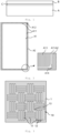
- Fig. 1 is a schematic structural view of an embodiment of the display panel according to the present disclosure.
- Fig. 2 is a schematic view of the layout of a display substrate in an embodiment of the display panel according to the present disclosure.
- the display panel includes: a display substrate A and a cover plate B.
- the cover plate B is located on a front side of the display substrate A along a light emitting direction of the display substrate A, that is, the cover plate B is on a light emitting side of the display substrate A.
- the display substrate A and the cover plate B may be encapsulated by an encapsulant adhesive C (such as optical clear adhesive or the like).
- the display substrate A has a display area A1 and a non-display area A2 surrounding the display area A1.
- the display substrate A may be encapsulated with the cover plate B in the non-display area A2.
- the material of the cover plate B may be a rigid or flexible material, such as a glass or a colorless polyimide (referred to as CPI for short) film.
- the display area A1 includes a plurality of sides A11, wherein adjacent sides A11 of the plurality of sides A11 intersect to form a plurality of corners A12.
- the display area A1 has two groups of opposite sides A11, and the adjacent sides A11 are perpendicular to each other. Accordingly, the display area A1 has four corners A12.
- the display area A1 includes a first display area A13 having a first pixel density and a second display area A14 having a second pixel density. The second pixel density is lower than the first pixel density.
- the pixel density of the transition area A15 between the first display area A13 and the second display area A14 may be equal to the first pixel density or the second pixel density, or located between the first pixel density and the second pixel density.
- the pixel density here refers to the number of pixels per unit area.
- the second display area A14 is located in at least one of the plurality of corners A12.
- a second display area A14 is provided in each of the four corners A12.
- a second display area having a pixel density lower than that of the first display area is provided in the corners, which on one hand, may realize the image display at the corners, thereby increasing the screen-to-body ratio, and reducing the display frame, and further allowing the user to obtain a better visual experience, and on the other hand, can also reduce the difficulty in the machining process of the corners.
- Fig. 3 is a schematic view of a plurality of opening patterns distributed along the surface of a stretchable base in an embodiment of the display panel according to the present disclosure.
- Fig. 4 is a schematic structural view of forming a portion of the display substrate corresponding to a second display area on the glass substrate in an embodiment of the display panel according to the present disclosure.
- Fig. 5 is a schematic structural view of disengaging a portion of the display substrate corresponding to the second display area from the glass substrate in an embodiment of the display panel according to the present disclosure.
- the second display area A14 includes: a stretchable base 1, a plurality of display units 2 and a plurality of wiring units 3.
- the stretchable base 1 may be made from a flexible material, such as polyimide (PI) .
- PI polyimide
- the stretchable base 1 includes a plurality of opening patterns 10 distributed along the surface of the stretchable base 1 (for example, the opening pattern formed by a plurality of openings within a dashed block in Fig. 3 ) .
- Each opening pattern 10 among the plurality of opening patterns 10 includes a plurality of first openings 11, wherein a plurality of bridge areas 12 configured to enclose an island area 13 are formed between at least some adjacent first openings 11 among the plurality of first openings 11.
- a plurality of opening patterns 10 are arranged in the stretchable base 1, so that the stretchable display of the second display area A14 may be realized.
- the stretchable display of the second display area it is possible to allow that the corners of the display area of the display substrate are more closely attached to the cover plate, thereby reducing or avoiding the conditions such as air bubbles that affect the attachment between the corners and the cover plate during encapsulation.
- a plurality of display units 2 are respectively arranged on the island area 13 formed by each opening pattern 10, and a plurality of wiring units 3 are respectively connected between the plurality of display units 2, and respectively arranged in the plurality of bridge areas 12.
- the display unit 2 has display sub-pixels (for example, RGB sub-pixels) and driving circuits, and can realize image display.
- the plurality of display units 2 are connected through the plurality of wiring units 3 respectively.
- the display substrate A is firstly formed on the glass substrate 4, and then the display substrate A is peeled from the glass substrate 4 after forming the display substrate.
- the entire film layer is bored at a corresponding position of the first opening 11, and the entire surface is coated (for example, the electrode layer and the inorganic encapsulation layer of the display substrate, or the like) at a corresponding position of the island area 13, the bridge area 12 and the first opening 11.
- Fig. 4 an opening is made in the display substrate A at a position corresponding to the first opening 11 along a direction perpendicular to the display substrate, and then the film layers such as the electrode layer and the inorganic encapsulation layer are evaporated on the entire surface, so that there are also film layers such as the electrode layer and the inorganic encapsulation layer within the first opening 11.
- the opening width of at least one of the plurality of first openings 11 gradually decreases along a light emitting direction of the display substrate A. That is, a first opening shape with a narrow top and a wide bottom is formed. At least part of the side wall of the first opening 11 form an included angle ⁇ with the surface of the stretchable base 1 on one side away from the plurality of display units and the plurality of wiring units. For example, part or entirety of the side wall of the first opening 11 on one side away from the cover plate B form an included angle ⁇ with the bottom surface of the stretchable base 1.
- the included angle ⁇ is about 50° to about 80°.
- such opening shape can make the opening wall on one side adjacent to the island area 13 and the opening wall on one side adjacent to the bridge area 12 within the first opening 11 both form a relatively flat section during peeling, thereby effectively improving the process.
- the film layer 15 at the bottom of the first opening 11 remains on the glass substrate 4.
- the flat section here means that there is a relatively flat disconnected part between the opening walls on both sides of the first opening 11 and the film layer 15, without a rugged section resulting from peeling of a local film layer or crack of an irregular film layer.
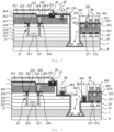
- Figs. 6 and 7 are respectively structural schematic views of forming a portion of the display substrate corresponding to the second display area on the glass substrate in some embodiments of the display panel according to the present disclosure.
- Figs. 8 and 9 are respectively schematic views of the arrangement of the island area, the first opening and the bridge area in some embodiments of the display panel according to the present disclosure.
- Figs. 10 and 11 are respectively schematic cross-sectional views of the first groove in some embodiments of the display panel according to the present disclosure.
- At least one of the plurality of display units 2 includes: a thin film transistor 22, a first planarization layer 241, a second electrode layer 243, a post spacer (referred to as PS for short) 26, a first organic light emitting layer 245, a first electrode layer 244, a first inorganic encapsulation layer 251, a first organic encapsulation layer 252, and a second inorganic encapsulation layer 253.
- the thin film transistor 22 is disposed on the stretchable base 1.
- the thin film transistor 22 includes an active layer 221, a gate 222, a first source 223, a first drain 224, a second source 225, and a second drain 226.
- the first source 223 and the first drain 224 are electrically connected to the active layer 221 through a via hole
- the second source 225 and the second drain 226 are respectively electrically connected to the first source 223 and the first drain 224 through a via hole.
- the thin film transistor 22 is not limited to the structural forms shown in Figs. 6 and 7 . In other embodiments, other structural forms may also be used.
- the thin film transistor includes a single-layer source and drain.
- the first planarization layer 241 is located on a front side of the stretchable base 1 along a light emitting direction of the display substrate, that is, on one side of the stretchable base 1 adjacent to the cover plate B. Specifically, the first planarization layer 241 is located on one side of the thin film transistor 22 away from the stretchable base 1, and covers the thin film transistor 22.
- the first planarization layer 241 may be configured to provide a flat surface for the formation of the upper film layer.
- the post spacer 26 is located on one side of the first planarization layer 241 away from the stretchable base 1, and has a first groove 27.
- the second electrode layer 243 is located on one side of the first planarization layer 241 away from the stretchable base 1, and electrically connected to the thin film transistor 22 through a via hole.
- the first organic light emitting layer 245 is located on one side of the second electrode layer 243 away from the stretchable base 1.
- the first electrode layer 244 is located on one side of the first organic light emitting layer 245 away from the stretchable base 1, and covers the post spacer 26.
- the first electrode layer 244 also covers the first organic light emitting layer 245.
- the second electrode layer 243 is an anode layer
- the first electrode layer 244 is a cathode layer.
- the second electrode layer 242, the first organic light emitting layer 245, and the first electrode layer 244 may form a light emitting element driven by the thin film transistor 22.
- different colors of sub-pixels may be realized according to different materials used in the first organic light-emitting layer 245.
- the first inorganic encapsulation layer 251 is located on one side of the first electrode layer 244 away from the stretchable base 1, and covers the first electrode layer 244.
- the first organic encapsulation layer 252 is located on one side of the first inorganic encapsulation layer 251 away from the stretchable base 1.
- the second inorganic encapsulation layer 253 is located on one side of the first organic encapsulation layer 252 away from the stretchable base 1, and covers the first organic encapsulation layer 252 and the first inorganic encapsulation layer 251.
- the first inorganic encapsulation layer 251 and the second inorganic encapsulation layer 253 may be formed by plasma enhanced chemical vapor deposition, and the first organic encapsulation layer 252 may be formed by printing.
- the first groove 27 provided on the post spacer 26 may implement controlling an edge position of the organic material.
- the first groove 27 is disposed on one side of the post spacer 26 away from the stretchable base 1 to block overflow of the organic material forming the first organic encapsulation layer 252.
- the first organic encapsulation layer 252 may cover part of the first inorganic encapsulation layer 251 located in the first groove 27 and part of the first groove 27 located away from the first opening 11, instead of covering part of the first inorganic encapsulation layer 251 between the first groove 27 and the first opening 11.
- the position of the first groove 27 may be determined according to the pitch and arrangement manner of the sub-pixels within the island area. In some embodiments, the distance between the first groove and the first opening 11 is less than about 30um.
- the first groove 27 may be completed through an exposure and development process.
- an organic material is printed, after the organic material flows to the first groove 27, it is not easily to continue to overflow to one side of the first groove 27 adjacent to the first opening.
- the first groove 27 includes a continuous groove 27a extending along a length direction of the first opening 11.
- the continuous groove 27a has a width w1 of about 5um to about 15 ⁇ m, and a height h1 of about 1.5 ⁇ m to about 2.5um.
- the width w1 here refers to the size of the continuous groove 27a in the post spacer 26 along a direction perpendicular to the first opening 11, and the height h1 refers to the size of the continuous groove 27a in the post spacer 26 along a direction perpendicular to the stretchable base 1.
- the first groove 27 includes at least one row of discrete grooves 27b arranged along a direction perpendicular to the length direction of the first opening 11, wherein each row of discrete grooves 27b includes a plurality of discrete grooves 27b arranged at intervals along the length direction of the first opening 11.
- the plurality of discrete grooves 27b has a width w2 of about 5um to about 10pm, and a height h2 of about 1.5 ⁇ m to about 2.5um.
- the width w2 here refers to the size of each discrete groove 27b in the post spacer 26 along a direction perpendicular to the first opening 11, and the height h2 refers to the size of each discrete groove 27b in the post spacer 26 along a direction perpendicular to the stretchable base 1.
- At least one row of discrete grooves 27b includes a plurality of rows of discrete grooves 27b (for example, two rows of discrete grooves) .
- the distance d between adjacent rows of discrete grooves 27b among the plurality of rows of discrete grooves 27b is about 2um to about 7um.
- the spacing d here refers to the distance between the adjacent rows of discrete grooves 27b in the post spacer 26 along a direction perpendicular to the first opening 11.
- some film layers for example, organic light-emitting layer or electrode layer
- some film layers are formed by plating the entire surface within the second display area. Accordingly, in order to prevent a failure risk resulting from the film layer corresponding to the first opening in communication with the film layer corresponding to the island area, in some embodiments, a first isolation structure is provided between the first groove 27 and the first opening 11 to achieve the isolation effect of the film layer.
- At least one of the plurality of display units 2 further includes first isolation structures 28, 28'.
- the first isolation structure 28, 28' is located between the first groove 27 and the first opening 11, and configured to disconnect the first electrode layer 244 on both sides of the first isolation structure 28, 28', so as to increase a transverse effective encapsulation distance.
- the first electrode layer 244 is covered on the first isolation structure 28, 28', and located on one side of the first isolation structure 28, 28' adjacent to the first groove and one side adjacent to the first opening 11.
- At least one of the plurality of display units 2 further includes: a first passivation layer 235.
- the first passivation layer 235 is located between the post spacer 26 and the first opening 11, and at least part of the first passivation layer 235 is located on one side of the first planarization layer 241 away from the stretchable base 1.
- at least one of the plurality of display units 2 may further include a first buffer layer 21, a first gate insulating layer 231, a second gate insulating layer 232, an interlayer insulating layer 233, and a second passivation layer 234.
- the lateral film layer formed at a position of the first planarization layer adjacent to the first opening (that is, a portion of the first inorganic encapsulation layer and the second inorganic encapsulation layer located on the first opening sidewall) is relatively thin due to a large height difference, and the water vapor from the side of the first opening 11 might enter devices such as the thin film transistor via the first planarization layer from a thin lateral film layer, thereby causing failure of the device.
- the first passivation layer 235 includes a first portion located on one side of the first planarization layer 241 away from the stretchable base 1, and a second portion located on one side of the first planarization layer 241 adjacent to the first opening 11.
- the second portion is connected to the surface of the second passivation layer 234 to form the isolation protection of the first passivation layer 235 on the surface of the first planarization layer 241 on one side adjacent to the first opening 11, thereby reducing or avoiding a risk of water vapor from the side of the first opening 11 entering devices such as the thin film transistor through the first planarization layer.
- the material of the first passivation layer 235 is the same as that of the second passivation layer 234 so as to achieve a more tight engagement therebetween.
- the first buffer layer 21 is located on one side of the stretchable base 1 adjacent to the first planarization layer 241.
- the first gate insulating layer 231 is located on one side of the first buffer layer 21 away from the stretchable base 1, and covers the active layer 221 of the thin film transistor 22.
- the second gate insulating layer 232 is located on one side of the first gate insulating layer 231 away from the stretchable base 1, and covers the gate 222 of the thin film transistor 22.
- the interlayer insulating layer 233 is located on one side of the second gate insulating layer 232 away from the stretchable base 1.
- the second passivation layer 234 is located between the interlayer insulating layer 233 and the first planarization layer 241.
- the first passivation layer 235 is located on one side of the first planarization layer 241 away from the stretchable base 1, and located between the post spacer 26 and the first opening 11.
- the gate 222 of the thin film transistor 22 is located on the surface of one side of the first gate insulating layer 231 away from the stretchable base 1.
- the first source 223 and the first drain 224 of the thin film transistor 22 are located on the surface of one side of the interlayer insulating layer 233 away from the stretchable base 1, and electrically connected to the active layer 221 through a via hole penetrating the first gate insulating layer 231, the second gate insulating layer 232 and the interlayer insulating layer 233.
- the second source 225 and the second drain 226 of the thin film transistor 22 are located on the surface of one side of the second passivation layer 234 away from the stretchable base 1, and electrically connected to the active layer 221 through a via hole penetrating the second passivation layer 234.
- the display unit 2 includes only the first gate insulating layer 231, but not the second gate insulating layer 232.
- the thin film transistor 22 includes a single-layer source and drain.
- the first isolation structure 28 includes at least one second groove 281 located in the first passivation layer 235.
- the first electrode layer 244 covering the bottom of the at least one second groove 281 and the first electrode layer 244 covering the surface of the first passivation layer 235 are disconnected from each other.
- the at least one second groove 281 has a width w3 of about 3 ⁇ m to about 10pm, and a height h3 of about 1000nm to about 3000nm.
- the width w3 here refers to the size of each second groove 281 along a direction perpendicular to the first opening 11, and the height h3 refers to the size of each second groove 281 along a direction perpendicular to the stretchable base 1.
- At least one of the plurality of wiring units 3 includes: a second planarization layer 331, a pixel definition layer 332 and a third electrode layer 333.
- the second planarization layer 331 is located on a front side of the stretchable base 1 along a light emitting direction of the display substrate, that is, on one side of the stretchable base 1 adjacent to the cover plate B.
- the pixel definition layer 332 is located on one side of the second planarization layer 331 away from the stretchable base 1, covers part of the surface of the second planarization layer 331, and has at least one third groove 361.
- At least one of the plurality of wiring units 3 further includes: a second buffer layer 31, a first conductive wiring 371, a gate insulating layer 32 and a second conductive wiring 372.
- the second buffer layer 31 is located on the surface of the stretchable base 1.
- the first conductive wiring 371 is located on the surface of the second buffer layer 31 on one side away from the stretchable base 1.
- the gate insulating layer 32 is located on one side of the second buffer layer 31 away from the stretchable base 1, and covers the first conductive wiring 371.
- the second conductive wiring 372 is located on the surface of one side of the gate insulating layer 32 away from the stretchable base 1.
- the second planarization layer 331 is located on one side of the second conductive wiring 372 away from the stretchable base 1, and covers the second conductive wiring 372.
- At least one third groove 361 is disposed adjacent to the first opening 11.
- the third electrode layer 333 covers the bottom of the at least one third groove 361, the surface of the pixel definition layer 332, and part of the surface of the second planarization layer 331 that is not covered by the pixel definition layer 332 .
- the third electrode layer 333 covering the bottom of the at least one third groove 361 and the third electrode layer 333 covering the surface of the pixel defining layer 332 are disconnected from each other, so that the third electrode layer 333 located in the bridge area is partitioned from the third electrode layer 333 corresponding to the first opening 11, so as to prevent the film layer corresponding to the first opening from communicating with the film layer corresponding to the island area via the film layer corresponding to the bridge area.
- the display substrate is formed on the glass substrate 4, and then peeled by laser.
- the corresponding film layers respectively provided in the island area and the bridge area may be located in the same layer and have the same material to simplify the process.
- the same material in the same layer here and later may be a layer structure formed by using the same film forming process to form a film layer for forming a specific pattern, and then using the same mask plate to pattern the film layer through a single patterning process.
- a single patterning process may include a plurality of exposure, development or etching processes, and the specific pattern in the formed layer structure may be continuous or discontinuous. These specific patterns might also be at different heights or have different thicknesses.
- the second buffer layer 31 and the first buffer layer 21 are located in the same layer and have the same material.
- the first conductive wiring 371 and part of the sources and drains of the thin film transistor 22 are located in the same layer and have the same material
- the second conductive wiring 372 and part of the sources and drains of the thin film transistor 22 are located in the same layer and have the same material
- the second planarization layer 331 and the first planarization layer 241 are located in the same layer and have the same material
- the third electrode layer 333 and the first electrode layer 244 are located in the same layer and have the same material.
- the number of third grooves 361 in at least one third groove 361 is the same as the number of second grooves 281 in the at least one second groove 281.
- the at least one third groove 361 and the at least one second groove 281 respectively communicate with each other to form a closed ring around the first opening 11.
- the two second grooves 281 (281a, 281b) of the first opening 11 on one side adjacent to the sub-pixel in the island area respectively communicate with the two third grooves 361 (361a, 361b) of the first opening 12 on one side adjacent to the bridge area.
- the first isolation structure 28' includes at least one first bump 282 located on the surface of the interlayer insulating layer 233 on one side away from the stretchable base 1.
- the first electrode layer 244 covers the top of the at least one first bump 282 and the surface of the interlayer insulating layer 233.
- the first electrode layer 244 located on the top of the at least one first bump 282 and the first electrode layer 244 located on the surface of the interlayer insulating layer 233 are disconnected from each other.
- the at least one first bump has a width w4 of about 3 ⁇ m to about 10pm, and a height h4 of about 400nm to about 800nm.
- the width w4 here refers to the size of each first bump 282 along a direction perpendicular to the first opening 11, and the height h4 refers to the size of each first bump 282 along a direction perpendicular to the stretchable base 1.
- the material of the first bump 282 may be a Ti-Al-Ti three-layer structure.
- At least one of the plurality of wiring units 3 includes: a gate insulating layer 32, at least one second bump 362 and a third electrode layer 333.
- the gate insulating layer 32 is located on a front side of the stretchable base 1 along a light emitting direction of the display substrate, that is, on one side of the stretchable base 1 adjacent to the cover plate B.
- At least one second bump 362 is located on the surface of one side of the gate insulating layer 32 away from the stretchable base 1.
- At least one of the plurality of wiring units 3 may further include: a second buffer layer 31, a first conductive wiring 371, a second conductive wiring 372, a second planarization layer 331, and a pixel definition layer 332.
- the second buffer layer 31 is located on the surface of the stretchable base 1.
- the first conductive wiring 371 is located on the surface of one side of the second buffer layer 31 away from the stretchable base 1.
- the third gate insulating layer 32 is located on one side of the second buffer layer 31 away from the stretchable base 1, and covers the first conductive wiring 371.
- the second conductive wiring 372 is located on the surface of one side of the third gate insulating layer 32 away from the stretchable base 1.
- the second planarization layer 331 is located on one side of the second conductive wiring 372 away from the stretchable base 1, and covers the second conductive wiring 372.
- the pixel definition layer 332 is located on one side of the second planarization layer 331 away from the stretchable base 1, and covers part of the surface of the second planarization layer 331.
- At least one second bump 362 may be disposed adjacent to the first opening 11.
- the third electrode layer 333 covers the top of the at least one second bump 362 and part of the surface of the third gate insulating layer 32 that is not covered by the third gate insulating layer 32.
- the third electrode layer 333 covering the top of the at least one second bump 362 and the third electrode layer 333 covering the surface of the third gate insulating layer 32 are disconnected from each other, so that the third electrode layer 333 located in the bridge area is partitioned from the third electrode layer 333 corresponding to the first opening 11, so as to prevent the film layer corresponding to the first opening from communicating with the film layer corresponding to the island area via the film layer corresponding to the bridge area.
- the corresponding film layers respectively provided in the island area and the bridge area may be located in the same layer and have the same material.
- the second buffer layer 31 and the first buffer layer 21 are located in the same layer and have the same material.
- the first conductive wiring 371 and part of the sources and drains of the thin film transistor 22 are located in the same layer and have the same material
- the second conductive wiring 372 and part of the sources and drains of the thin film transistor 22 are located in the same layer and have the same material
- the second planarization layer 331 and the first planarization layer 241 are located in the same layer and have the same material
- the third electrode layer 333 and the first electrode layer 244 are located in the same layer and have the same material.
- the number of second bumps 362 in the at least one second bump 362 is the same as the number of first bumps 282 in the at least one first bump 282, and respectively communicate with each other to form a closed ring around the first opening 11.
- the second bump 362 and the first bump 282 may be formed in the same patterning process.
- At least one of the plurality of wiring units 3 may include: at least one inorganic encapsulation layer and an organic coating 343.
- the at least one inorganic encapsulation layer is located on a front side of the stretchable base 1 along a light emitting direction of the display substrate, that is, on one side of the stretchable base 1 adjacent to the cover plate B.
- the organic coating 343 is located on a front side of the inorganic encapsulation layer farthest away from the stretchable base in the at least one inorganic encapsulation layer along a light emitting direction of the display substrate A, and has a coating pattern. In the case of meeting the reliability requirements of the product, it is possible not to provide other film layers between the organic coating 343 and the cover plate B, so that the display substrate can be flexibly attached to the cover plate at a position corresponding to the bridge area.
- the at least one inorganic encapsulation layer may include: a third inorganic encapsulation layer 341 and a fourth inorganic encapsulation layer 342.
- the third inorganic encapsulation layer 341 is located on one side of the third electrode layer 333 away from the stretchable base 1.
- the fourth inorganic encapsulation layer 342 is located on one side of the third inorganic encapsulation layer 341 away from the third inorganic encapsulation layer 341.
- the organic coating 343 is located on one side of the fourth inorganic encapsulation layer 342 away from the fourth inorganic encapsulation layer 342.
- the third inorganic encapsulation layer 341 and the fourth inorganic encapsulation layer 342 may be formed by plasma enhanced chemical vapor deposition, and the organic coating 343 may be formed by coating.
- the material of the organic coating 343 may be 1-methoxy-2-propyl acetate, acrylic acid polymers, etc.
- the third electrode layer 333 and the first electrode layer 244 are located in the same layer and have the same material, and the third inorganic encapsulation layer 341 may be located in the same layer and have the same material as the first inorganic encapsulation layer 251.
- the encapsulation layer 342 may be located in the same layer and have the same material as the second inorganic encapsulation layer 253, so as to simplify the process.
- the coating pattern in the organic coating 343 includes at least one second opening 39, and the length direction of the at least one second opening 39 is parallel to the length direction of the adjacent first opening 11.
- the coating pattern includes a plurality of second openings 39 parallel to each other.
- the second opening 39 of the coating pattern may be formed by an exposure and development process . With the second opening of the organic coating in the bridge area, the tensile properties of the bridge area can be effectively improved.
- the above-mentioned embodiments of the display panel of the present disclosure are applicable to various display devices. Therefore, the present disclosure also provides a display device including the aforementioned display panel.
- the display device may be any product or component with a display function, such as a mobile phone, a tablet computer, a television, a monitor, a notebook computer, a digital photo frame, a navigator and the like.
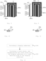
- Fig. 12 is a schematic flowchart of an embodiment of a manufacturing method of the display panel according to the present disclosure.
- the method of manufacturing a display panel includes: step 100 and step 200.
- step 100 a display substrate A is provided.
- the display substrate has a display area A1 and a non-display area A2 surrounding the display area A1.
- the display area A1 includes a plurality of sides A11, wherein adjacent sides A11 of the plurality of sides A11 intersect to form a plurality of corners A12, the display area A1 includes a first display area A13 with a first pixel density and a second display area A14 with a second pixel density lower than the first pixel density, and the second display area A14 is located in at least one of the plurality of corners A12.
- a cover plate B is provided, and the cover plate is encapsulated with the display substrate A on a light emitting side of the display substrate A.
Landscapes
- Engineering & Computer Science (AREA)
- Microelectronics & Electronic Packaging (AREA)
- Physics & Mathematics (AREA)
- Chemical & Material Sciences (AREA)
- Inorganic Chemistry (AREA)
- Geometry (AREA)
- General Physics & Mathematics (AREA)
- Theoretical Computer Science (AREA)
- Manufacturing & Machinery (AREA)
- Electroluminescent Light Sources (AREA)
- Devices For Indicating Variable Information By Combining Individual Elements (AREA)
Abstract
Description
- The present disclosure relates to the field of display, and in particular to a display substrate, a display panel, a display device, and a manufacturing method of a display panel.
- The organic light-emitting diode (referred to as OLED for short) has an organic compound film that emits light in response to current, wherein an organic material is interposed between two electrodes, and at least one electrode is a light-transmitting electrode. The OLED, which has a favorable light-emitting performance and efficiency, and requires a lower driving voltage, is a favorable priority for use as a display screen.
- In one aspect of the present disclosure, a display substrate is provided. The display substrate includes a display area, the display area including: a plurality of sides, wherein adjacent sides of the plurality of sides intersect to form a plurality of corners; a first display area having a first pixel density; and a second display area having a second pixel density lower than the first pixel density, wherein the second display area is located in at least one of the corners.
- In some embodiments, the second display area includes: a stretchable base including a plurality of opening patterns distributed along a surface of the stretchable base, wherein each of the plurality of opening patterns includes a plurality of first openings, and a plurality of bridge areas configured to enclose an island area are formed between at least part of adj acent first openings among the plurality of first openings; a plurality of display units respectively arranged on island areas formed by respective opening patterns; and a plurality of wiring units respectively connected between the plurality of display units and respectively arranged in the plurality of bridge areas.
- In some embodiments, at least one of the plurality of display units includes: a first planarization layer located on a front side of the stretchable base along a light emitting direction of the display substrate; a post spacer located on one side of the first planarization layer away from the stretchable base, and having a first groove; a first electrode layer located on one side of the first planarization layer away from the stretchable base and covering the post spacer; a first inorganic encapsulation layer located on one side of the first electrode layer away from the stretchable base and covering the first electrode layer; and a first organic encapsulation layer covering part of the first inorganic encapsulation layer located in the first groove and a part of the first groove on one side away from the first opening, and not covering part of the first inorganic encapsulation layer between the first groove and the first opening.
- In some embodiments, the first groove includes a continuous groove extending along a length direction of the first opening.
- In some embodiments, the continuous groove has a width of about 5um to about 15µm and a height of about 1.5µm to about 2.5um.
- In some embodiments, the first groove includes at least one row of discrete grooves arranged along a direction perpendicular to a length direction of the first opening, and each row of discrete grooves includes a plurality of discrete grooves arranged at intervals along a length direction of the first opening.
- In some embodiments, the plurality of discrete grooves have a width of about 5um to about 10pm, and a height of about 1.5µm to about 2.5um.
- In some embodiments, the at least one row of discrete grooves includes a plurality of rows of discrete grooves, and a distance between adjacent rows of discrete grooves among the plurality of rows of discrete grooves is about 2um to about 7um.
- In some embodiments, a distance between the first groove and the first opening is less than about 30um.
- In some embodiments, at least one of the plurality of display units further includes: a first isolation structure located between the first groove and the first opening, and configured to disconnect the first electrode layers on both sides of the first isolation structure, wherein the first electrode layer covers the first isolation structure, and is located on one side of the first isolation structure adjacent to the first groove and one side of the first isolation structure adjacent to the first opening.
- In some embodiments, at least one of the plurality of display units further includes: a first passivation layer located between the post spacer and the first opening, and at least part of the first passivation layer being located on one side of the first planarization layer away from the stretchable base; wherein the first isolation structure includes at least one second groove located in the first passivation layer and the first planarization layer, and the first electrode layer covering a bottom of the at least one second groove and the first electrode layer covering a surface of the first passivation layer are disconnected from each other.
- In some embodiments, the at least one second groove has a width of about 3µm to about 10pm and a height of about 1000nm to about 3000nm.
- In some embodiments, at least one of the plurality of display units further includes: an interlayer insulating layer located on a front side of the stretchable base along a light emitting direction of the display substrate; and wherein the first isolation structure includes at least one first bump located on a surface of the interlayer insulating layer on one side away from the stretchable base, the first electrode layer covers a top of the at least one first bump and part of a surface of the interlayer insulating layer, the first electrode layer on the top of the at least one first bump and the first electrode layer on the surface of the interlayer insulating layer are disconnected from each other.
- In some embodiments, the at least one first bump has a width of about 3µm to about 10pm, and a height of about 400nm to about 800nm.
- In some embodiments, at least one of the plurality of wiring units includes: a second planarization layer located on a front side of the stretchable base along a light emitting direction of the display substrate; a pixel definition layer located on one side of the second planarization layer away from the stretchable base, covering part of a surface of the second planarization layer, and having at least one third groove; and a third electrode layer covering a bottom of the at least one third groove, a surface of the pixel definition layer and part of a surface of the second planarization layer that is not covered by the pixel definition layer; wherein the third electrode layer covering the bottom of the at least one third groove and the third electrode layer covering the surface of the pixel definition layer are disconnected from each other.
- In some embodiments, the number of third grooves in the at least one third groove is equal to the number of second grooves in the at least one second groove, and the at least one third groove and the at least one second groove respectively communicate with each other to form a closed ring around the first opening.
- In some embodiments, at least one of the plurality of wiring units includes: a gate insulating layer located on a front side of the stretchable base along a light emitting direction of the display substrate; at least one second bump located on a surface of the gate insulating layer on one side away from the stretchable base; and a third electrode layer covering a top of the at least one second bump and part of a surface of the gate insulating layer that is not covered by the at least one second bump, wherein the third electrode layer covering the top of the at least one second bump and the third electrode layer covering the surface of the gate insulating layer are disconnected from each other.
- In some embodiments, the number of second bumps in the at least one second bump is equal to the number of first bumps in the at least one first bump, and the at least one second bump and the at least one first bump respectively communicate with each other to form a closed ring around the first opening.
- In some embodiments, a opening width of at least one of the plurality of first openings gradually decreases along a light emitting direction of the display substrate, and at least part of a sidewall of the opening forms an included angle with a surface of the stretchable base on one side away from the plurality of display units and the plurality of wiring units.
- In some embodiments, the included angle is about 50° to about 80° .
- In some embodiments, at least one of the plurality of wiring units includes: at least one inorganic encapsulation layer located on a front side of the stretchable base along a light emitting direction of the display substrate; and an organic coating located on a front side of the inorganic encapsulation layer farthest away from the stretchable base in the at least one inorganic encapsulation layer along a light emitting direction of the display substrate, and having a coating pattern.
- In some embodiments, the coating pattern includes at least one second opening having a length direction parallel to a length direction of an adjacent first opening.
- In one aspect of the present disclosure, a display panel is provided. The display panel includes: the display substrate described above; and a cover plate located on a light emitting side of the display substrate and encapsulated with the display substrate.
- In one aspect of the present disclosure, a display device is provided. The display device includes: the display panel described above.
- In one aspect of the present disclosure, a manufacturing method of a display panel is provided. The method includes the steps of: providing a display substrate, wherein the display substrate has a display area, the display area includes a plurality of sides, wherein adjacent sides of the plurality of sides intersect to form a plurality of corners, and the display area includes a first display area with a pixel density and a second display area with a second pixel density lower than the first pixel density, and the second display area is located in at least one of the plurality of corners; providing a cover plate, and encapsulating the cover plate with the display substrate on a light emitting side of the display substrate.
- The accompanying drawings, which constitute part of this specification, illustrate exemplary embodiments of the present disclosure and, together with this specification, serve to explain the principles of the present disclosure.
- The present disclosure may be more clearly understood from the following detailed description with reference to the accompanying drawings, in which:
-
Fig. 1 is a schematic structural view of an embodiment of the display panel according to the present disclosure; -
Fig. 2 is a schematic view of the layout of a display substrate in an embodiment of the display panel according to the present disclosure; -
Fig. 3 is a schematic view of a plurality of opening patterns distributed along the surface of a stretchable base in an embodiment of the display panel according to the present disclosure; -
Fig. 4 is a schematic structural view of forming a portion of the display substrate corresponding to a second display area on the glass substrate in an embodiment of the display panel according to the present disclosure; -
Fig. 5 is a schematic structural view of disengaging a portion of the display substrate corresponding to the second display area from the glass substrate in an embodiment of the display panel according to the present disclosure; -
Figs. 6 and 7 are respectively structural schematic views of forming a portion of the display substrate corresponding to the second display area on the glass substrate in some embodiments of the display panel according to the present disclosure; -
Figs. 8 and 9 are respectively schematic views of the arrangement of the island area, the first opening and the bridge area in some embodiments of the display panel according to the present disclosure; -
Figs. 10 and 11 are respectively schematic cross-sectional views of the first groove in some embodiments of the display panel according to the present disclosure; -
Fig. 12 is a schematic flowchart of an embodiment of a manufacturing method of the display panel according to the present disclosure. - It should be understood that the sizes of the various parts shown in the accompanying drawings are not drawn according to the actual scale. In addition, the same or similar reference signs are used to denote the same or similar components.
- Various exemplary embodiments of the present disclosure will now be described in detail with reference to the accompanying drawings. The description of the exemplary embodiments is merely illustrative and is in no way intended as a limitation to the present disclosure, its application or use. The present disclosure may be implemented in many different forms, which are not limited to the embodiments described herein. These embodiments are provided to make the present disclosure thorough and complete, and fully convey the scope of the present disclosure to those skilled in the art. It should be noticed that: relative arrangement of components and steps, material composition, numerical expressions, and numerical values set forth in these embodiments, unless specifically stated otherwise, should be explained as merely illustrative, and not as a limitation.
- The words "first", "second", and similar words used in the present disclosure do not denote any order, quantity or importance, but merely serve to distinguish different parts. Such similar words as "comprising" or "including" mean that the element preceding the word encompasses the elements enumerated after the word, and does not exclude the possibility of encompassing other elements as well. The terms "up", "down", "left", "right", or the like are used only to represent a relative positional relationship, and the relative positional relationship may be changed correspondingly if the absolute position of the described object changes.
- In the present disclosure, when it is described that a particular device is located between the first device and the second device, there may be an intermediate device between the particular device and the first device or the second device, and alternatively, there may be no intermediate device. When it is described that a particular device is connected to other devices, the particular device may be directly connected to said other devices without an intermediate device, and alternatively, may not be directly connected to said other devices but with an intermediate device.
- All the terms (including technical and scientific terms) used in the present disclosure have the same meanings as understood by those skilled in the art of the present disclosure unless otherwise defined. It should also be understood that terms as defined in general dictionaries, unless explicitly defined herein, should be interpreted as having meanings that are consistent with their meanings in the context of the relevant art, and not to be interpreted in an idealized or extremely formalized sense.
- In the present disclosure, the term "about" refers to a numerical range and/or value that are/is substantially the same as those value ranges and/or values listed herein within the allowable process errors and measurement error ranges.
- Techniques, methods, and apparatus known to those of ordinary skill in the relevant art may not be discussed in detail, but where appropriate, these techniques, methods, and apparatuses should be considered as part of this specification.
- In some related technologies, the flexible OLED uses a polymer material as a protective cover, and the formed OLED device is not fragile. The inventors have found through research that some OLED flexible display devices are present with a black margin phenomenon at the four corners, which affects the user's visual experience.
- In view of this, the embodiments of the present disclosure provide a display substrate, a display panel, a display device, and a manufacturing method of the display panel, which can improve the user's visual experience.
-
Fig. 1 is a schematic structural view of an embodiment of the display panel according to the present disclosure.Fig. 2 is a schematic view of the layout of a display substrate in an embodiment of the display panel according to the present disclosure. - Referring to
Figs. 1 and 2 , in some embodiments, the display panel includes: a display substrate A and a cover plate B. The cover plate B is located on a front side of the display substrate A along a light emitting direction of the display substrate A, that is, the cover plate B is on a light emitting side of the display substrate A. The display substrate A and the cover plate B may be encapsulated by an encapsulant adhesive C (such as optical clear adhesive or the like). InFig. 2 , the display substrate A has a display area A1 and a non-display area A2 surrounding the display area A1. The display substrate A may be encapsulated with the cover plate B in the non-display area A2. The material of the cover plate B may be a rigid or flexible material, such as a glass or a colorless polyimide (referred to as CPI for short) film. - Referring to
Fig. 2 , the display area A1 includes a plurality of sides A11, wherein adjacent sides A11 of the plurality of sides A11 intersect to form a plurality of corners A12. InFig. 2 , the display area A1 has two groups of opposite sides A11, and the adjacent sides A11 are perpendicular to each other. Accordingly, the display area A1 has four corners A12. The display area A1 includes a first display area A13 having a first pixel density and a second display area A14 having a second pixel density. The second pixel density is lower than the first pixel density. - The pixel density of the transition area A15 between the first display area A13 and the second display area A14 may be equal to the first pixel density or the second pixel density, or located between the first pixel density and the second pixel density. The pixel density here refers to the number of pixels per unit area.
- Referring to
Fig. 2 , in some embodiments, the second display area A14 is located in at least one of the plurality of corners A12. InFig. 2 , a second display area A14 is provided in each of the four corners A12. Considering that the corners of the display substrate and the cover plate are filled and encapsulated with organic ink therebetween in some related technologies, which results in a black margin appearing at the corners, in this embodiment, a second display area having a pixel density lower than that of the first display area is provided in the corners, which on one hand, may realize the image display at the corners, thereby increasing the screen-to-body ratio, and reducing the display frame, and further allowing the user to obtain a better visual experience, and on the other hand, can also reduce the difficulty in the machining process of the corners. -
Fig. 3 is a schematic view of a plurality of opening patterns distributed along the surface of a stretchable base in an embodiment of the display panel according to the present disclosure.Fig. 4 is a schematic structural view of forming a portion of the display substrate corresponding to a second display area on the glass substrate in an embodiment of the display panel according to the present disclosure.Fig. 5 is a schematic structural view of disengaging a portion of the display substrate corresponding to the second display area from the glass substrate in an embodiment of the display panel according to the present disclosure. - Referring to
Figs. 3 to 5 , in some embodiments, the second display area A14 includes: astretchable base 1, a plurality ofdisplay units 2 and a plurality ofwiring units 3. Thestretchable base 1 may be made from a flexible material, such as polyimide (PI) . Referring toFig. 3 , thestretchable base 1 includes a plurality of openingpatterns 10 distributed along the surface of the stretchable base 1 (for example, the opening pattern formed by a plurality of openings within a dashed block inFig. 3 ) . Eachopening pattern 10 among the plurality of openingpatterns 10 includes a plurality offirst openings 11, wherein a plurality ofbridge areas 12 configured to enclose anisland area 13 are formed between at least some adjacentfirst openings 11 among the plurality offirst openings 11. A plurality of openingpatterns 10 are arranged in thestretchable base 1, so that the stretchable display of the second display area A14 may be realized. By way of the stretchable display of the second display area, it is possible to allow that the corners of the display area of the display substrate are more closely attached to the cover plate, thereby reducing or avoiding the conditions such as air bubbles that affect the attachment between the corners and the cover plate during encapsulation. - In
Fig. 3 , threefirst openings 11 are respectively provided around theisland area 13 of theopening pattern 10, and twobridge areas 12 can be formed between adjacentfirst openings 11 of the threefirst openings 11. In other embodiments, the positions of thefirst openings 11 around theisland area 13 relative to theisland area 13 and the number of thefirst openings 11 are not limited to the circumstances shown inFig. 3 . Thefirst opening 11 may have a width of about 15µm to about 25um. Referring toFig. 4 , in some embodiments, a plurality ofdisplay units 2 are respectively arranged on theisland area 13 formed by each openingpattern 10, and a plurality ofwiring units 3 are respectively connected between the plurality ofdisplay units 2, and respectively arranged in the plurality ofbridge areas 12. Thedisplay unit 2 has display sub-pixels (for example, RGB sub-pixels) and driving circuits, and can realize image display. The plurality ofdisplay units 2 are connected through the plurality ofwiring units 3 respectively. - Referring to
Figs. 4 and 5 , in some embodiments, the display substrate A is firstly formed on theglass substrate 4, and then the display substrate A is peeled from theglass substrate 4 after forming the display substrate. During the process of forming the display substrate, the entire film layer is bored at a corresponding position of thefirst opening 11, and the entire surface is coated (for example, the electrode layer and the inorganic encapsulation layer of the display substrate, or the like) at a corresponding position of theisland area 13, thebridge area 12 and thefirst opening 11. - When the display substrate A is peeled (for example, peeled by laser), it is found through research that there is a risk of peeling of a film layer and crack of a local irregular film layer between the film layer located in the
first opening 11 and the film layer located in the island area during peeling by laser. To solve such process risk, inFig. 4 , an opening is made in the display substrate A at a position corresponding to thefirst opening 11 along a direction perpendicular to the display substrate, and then the film layers such as the electrode layer and the inorganic encapsulation layer are evaporated on the entire surface, so that there are also film layers such as the electrode layer and the inorganic encapsulation layer within thefirst opening 11. - In some embodiments, the opening width of at least one of the plurality of
first openings 11 gradually decreases along a light emitting direction of the display substrate A. That is, a first opening shape with a narrow top and a wide bottom is formed. At least part of the side wall of thefirst opening 11 form an included angle α with the surface of thestretchable base 1 on one side away from the plurality of display units and the plurality of wiring units. For example, part or entirety of the side wall of thefirst opening 11 on one side away from the cover plate B form an included angle α with the bottom surface of thestretchable base 1. - In some embodiments, the included angle α is about 50° to about 80°. After verification of peeling by laser, such opening shape can make the opening wall on one side adjacent to the
island area 13 and the opening wall on one side adjacent to thebridge area 12 within thefirst opening 11 both form a relatively flat section during peeling, thereby effectively improving the process. After peeling, thefilm layer 15 at the bottom of thefirst opening 11 remains on theglass substrate 4. The flat section here means that there is a relatively flat disconnected part between the opening walls on both sides of thefirst opening 11 and thefilm layer 15, without a rugged section resulting from peeling of a local film layer or crack of an irregular film layer. -
Figs. 6 and 7 are respectively structural schematic views of forming a portion of the display substrate corresponding to the second display area on the glass substrate in some embodiments of the display panel according to the present disclosure.Figs. 8 and 9 are respectively schematic views of the arrangement of the island area, the first opening and the bridge area in some embodiments of the display panel according to the present disclosure.Figs. 10 and 11 are respectively schematic cross-sectional views of the first groove in some embodiments of the display panel according to the present disclosure. - Referring to
Figs. 6 and 7 , in some embodiments, at least one of the plurality ofdisplay units 2 includes: athin film transistor 22, afirst planarization layer 241, asecond electrode layer 243, a post spacer (referred to as PS for short) 26, a first organiclight emitting layer 245, afirst electrode layer 244, a firstinorganic encapsulation layer 251, a firstorganic encapsulation layer 252, and a secondinorganic encapsulation layer 253. - In
Figs. 6 and 7 , thethin film transistor 22 is disposed on thestretchable base 1. Thethin film transistor 22 includes anactive layer 221, agate 222, afirst source 223, afirst drain 224, asecond source 225, and asecond drain 226. Thefirst source 223 and thefirst drain 224 are electrically connected to theactive layer 221 through a via hole, and thesecond source 225 and thesecond drain 226 are respectively electrically connected to thefirst source 223 and thefirst drain 224 through a via hole. Thethin film transistor 22 is not limited to the structural forms shown inFigs. 6 and 7 . In other embodiments, other structural forms may also be used. For example, the thin film transistor includes a single-layer source and drain. - The
first planarization layer 241 is located on a front side of thestretchable base 1 along a light emitting direction of the display substrate, that is, on one side of thestretchable base 1 adjacent to the cover plate B. Specifically, thefirst planarization layer 241 is located on one side of thethin film transistor 22 away from thestretchable base 1, and covers thethin film transistor 22. Thefirst planarization layer 241 may be configured to provide a flat surface for the formation of the upper film layer. - The
post spacer 26 is located on one side of thefirst planarization layer 241 away from thestretchable base 1, and has afirst groove 27. Thesecond electrode layer 243 is located on one side of thefirst planarization layer 241 away from thestretchable base 1, and electrically connected to thethin film transistor 22 through a via hole. - The first organic
light emitting layer 245 is located on one side of thesecond electrode layer 243 away from thestretchable base 1. Thefirst electrode layer 244 is located on one side of the first organiclight emitting layer 245 away from thestretchable base 1, and covers thepost spacer 26. Thefirst electrode layer 244 also covers the first organiclight emitting layer 245. - In some embodiments, the
second electrode layer 243 is an anode layer, and thefirst electrode layer 244 is a cathode layer. Thesecond electrode layer 242, the first organiclight emitting layer 245, and thefirst electrode layer 244 may form a light emitting element driven by thethin film transistor 22. In the island area, different colors of sub-pixels may be realized according to different materials used in the first organic light-emittinglayer 245. - Referring to
Figs. 6 and 7 , in some embodiments, the firstinorganic encapsulation layer 251 is located on one side of thefirst electrode layer 244 away from thestretchable base 1, and covers thefirst electrode layer 244. The firstorganic encapsulation layer 252 is located on one side of the firstinorganic encapsulation layer 251 away from thestretchable base 1. The secondinorganic encapsulation layer 253 is located on one side of the firstorganic encapsulation layer 252 away from thestretchable base 1, and covers the firstorganic encapsulation layer 252 and the firstinorganic encapsulation layer 251. - In order to ensure that the sub-pixels at a position adjacent to the first opening in the island area can emit light and prevent material failure and electrode corrosion, it is possible to perform encapsulation protection by a plurality of encapsulation layers. The first
inorganic encapsulation layer 251 and the secondinorganic encapsulation layer 253 may be formed by plasma enhanced chemical vapor deposition, and the firstorganic encapsulation layer 252 may be formed by printing. In order to avoid a risk of forming water and oxygen erosion paths between the outside and the first organic light-emittinglayer 245, and between the outside and thefirst electrode layer 244 resulting from the organic material (such as organic ink) for printing the firstorganic encapsulation layer 252 overflowing into the first opening, thefirst groove 27 provided on thepost spacer 26 may implement controlling an edge position of the organic material. - The
first groove 27 is disposed on one side of thepost spacer 26 away from thestretchable base 1 to block overflow of the organic material forming the firstorganic encapsulation layer 252. In this way, the firstorganic encapsulation layer 252 may cover part of the firstinorganic encapsulation layer 251 located in thefirst groove 27 and part of thefirst groove 27 located away from thefirst opening 11, instead of covering part of the firstinorganic encapsulation layer 251 between thefirst groove 27 and thefirst opening 11. - The position of the
first groove 27 may be determined according to the pitch and arrangement manner of the sub-pixels within the island area. In some embodiments, the distance between the first groove and thefirst opening 11 is less than about 30um. - In
Figs. 6 and 7 , thefirst groove 27 may be completed through an exposure and development process. When an organic material is printed, after the organic material flows to thefirst groove 27, it is not easily to continue to overflow to one side of thefirst groove 27 adjacent to the first opening. - Referring to
Fig. 8 , in some embodiments, thefirst groove 27 includes acontinuous groove 27a extending along a length direction of thefirst opening 11. Referring toFigs. 8 and 10 , thecontinuous groove 27a has a width w1 of about 5um to about 15µm, and a height h1 of about 1.5µm to about 2.5um. The width w1 here refers to the size of thecontinuous groove 27a in thepost spacer 26 along a direction perpendicular to thefirst opening 11, and the height h1 refers to the size of thecontinuous groove 27a in thepost spacer 26 along a direction perpendicular to thestretchable base 1. - Referring to
Fig. 9 , in some embodiments, thefirst groove 27 includes at least one row ofdiscrete grooves 27b arranged along a direction perpendicular to the length direction of thefirst opening 11, wherein each row ofdiscrete grooves 27b includes a plurality ofdiscrete grooves 27b arranged at intervals along the length direction of thefirst opening 11. Referring toFigs. 9 and 11 , the plurality ofdiscrete grooves 27b has a width w2 of about 5um to about 10pm, and a height h2 of about 1.5µm to about 2.5um. The width w2 here refers to the size of eachdiscrete groove 27b in thepost spacer 26 along a direction perpendicular to thefirst opening 11, and the height h2 refers to the size of eachdiscrete groove 27b in thepost spacer 26 along a direction perpendicular to thestretchable base 1. - In
Fig. 9 , at least one row ofdiscrete grooves 27b includes a plurality of rows ofdiscrete grooves 27b (for example, two rows of discrete grooves) . The distance d between adjacent rows ofdiscrete grooves 27b among the plurality of rows ofdiscrete grooves 27b is about 2um to about 7um. The spacing d here refers to the distance between the adjacent rows ofdiscrete grooves 27b in thepost spacer 26 along a direction perpendicular to thefirst opening 11. - In the manufacturing process of some embodiments of the display panel, some film layers (for example, organic light-emitting layer or electrode layer) are formed by plating the entire surface within the second display area. Accordingly, in order to prevent a failure risk resulting from the film layer corresponding to the first opening in communication with the film layer corresponding to the island area, in some embodiments, a first isolation structure is provided between the
first groove 27 and thefirst opening 11 to achieve the isolation effect of the film layer. - Referring to
Figs. 6 and 7 , in some embodiments, at least one of the plurality ofdisplay units 2 further includesfirst isolation structures 28, 28'. Thefirst isolation structure 28, 28' is located between thefirst groove 27 and thefirst opening 11, and configured to disconnect thefirst electrode layer 244 on both sides of thefirst isolation structure 28, 28', so as to increase a transverse effective encapsulation distance. Thefirst electrode layer 244 is covered on thefirst isolation structure 28, 28', and located on one side of thefirst isolation structure 28, 28' adjacent to the first groove and one side adjacent to thefirst opening 11. - Referring to
Fig. 6 , at least one of the plurality ofdisplay units 2 further includes: afirst passivation layer 235. Thefirst passivation layer 235 is located between thepost spacer 26 and thefirst opening 11, and at least part of thefirst passivation layer 235 is located on one side of thefirst planarization layer 241 away from thestretchable base 1. In addition, at least one of the plurality ofdisplay units 2 may further include afirst buffer layer 21, a firstgate insulating layer 231, a second gate insulating layer 232, aninterlayer insulating layer 233, and asecond passivation layer 234. - It is found through research that when the first inorganic encapsulation layer and the second inorganic encapsulation layer are formed by a plasma film forming process, the lateral film layer formed at a position of the first planarization layer adjacent to the first opening (that is, a portion of the first inorganic encapsulation layer and the second inorganic encapsulation layer located on the first opening sidewall) is relatively thin due to a large height difference, and the water vapor from the side of the
first opening 11 might enter devices such as the thin film transistor via the first planarization layer from a thin lateral film layer, thereby causing failure of the device. - In
Fig. 6 , thefirst passivation layer 235 includes a first portion located on one side of thefirst planarization layer 241 away from thestretchable base 1, and a second portion located on one side of thefirst planarization layer 241 adjacent to thefirst opening 11. The second portion is connected to the surface of thesecond passivation layer 234 to form the isolation protection of thefirst passivation layer 235 on the surface of thefirst planarization layer 241 on one side adjacent to thefirst opening 11, thereby reducing or avoiding a risk of water vapor from the side of thefirst opening 11 entering devices such as the thin film transistor through the first planarization layer. In some embodiments, the material of thefirst passivation layer 235 is the same as that of thesecond passivation layer 234 so as to achieve a more tight engagement therebetween. - The
first buffer layer 21 is located on one side of thestretchable base 1 adjacent to thefirst planarization layer 241. The firstgate insulating layer 231 is located on one side of thefirst buffer layer 21 away from thestretchable base 1, and covers theactive layer 221 of thethin film transistor 22. The second gate insulating layer 232 is located on one side of the firstgate insulating layer 231 away from thestretchable base 1, and covers thegate 222 of thethin film transistor 22. - The interlayer insulating
layer 233 is located on one side of the second gate insulating layer 232 away from thestretchable base 1. Thesecond passivation layer 234 is located between the interlayer insulatinglayer 233 and thefirst planarization layer 241. Thefirst passivation layer 235 is located on one side of thefirst planarization layer 241 away from thestretchable base 1, and located between thepost spacer 26 and thefirst opening 11. - The
gate 222 of thethin film transistor 22 is located on the surface of one side of the firstgate insulating layer 231 away from thestretchable base 1. Thefirst source 223 and thefirst drain 224 of thethin film transistor 22 are located on the surface of one side of the interlayer insulatinglayer 233 away from thestretchable base 1, and electrically connected to theactive layer 221 through a via hole penetrating the firstgate insulating layer 231, the second gate insulating layer 232 and the interlayer insulatinglayer 233. Thesecond source 225 and thesecond drain 226 of thethin film transistor 22 are located on the surface of one side of thesecond passivation layer 234 away from thestretchable base 1, and electrically connected to theactive layer 221 through a via hole penetrating thesecond passivation layer 234. In other embodiments, thedisplay unit 2 includes only the firstgate insulating layer 231, but not the second gate insulating layer 232. In other embodiments, thethin film transistor 22 includes a single-layer source and drain. - In
Fig. 6 , thefirst isolation structure 28 includes at least onesecond groove 281 located in thefirst passivation layer 235. Thefirst electrode layer 244 covering the bottom of the at least onesecond groove 281 and thefirst electrode layer 244 covering the surface of thefirst passivation layer 235 are disconnected from each other. Referring toFig. 6 , the at least onesecond groove 281 has a width w3 of about 3µm to about 10pm, and a height h3 of about 1000nm to about 3000nm. The width w3 here refers to the size of eachsecond groove 281 along a direction perpendicular to thefirst opening 11, and the height h3 refers to the size of eachsecond groove 281 along a direction perpendicular to thestretchable base 1. - Referring to
Fig. 6 , in some embodiments, at least one of the plurality ofwiring units 3 includes: asecond planarization layer 331, apixel definition layer 332 and athird electrode layer 333. Thesecond planarization layer 331 is located on a front side of thestretchable base 1 along a light emitting direction of the display substrate, that is, on one side of thestretchable base 1 adjacent to the cover plate B. Thepixel definition layer 332 is located on one side of thesecond planarization layer 331 away from thestretchable base 1, covers part of the surface of thesecond planarization layer 331, and has at least onethird groove 361. - In
Fig. 6 , at least one of the plurality ofwiring units 3 further includes: asecond buffer layer 31, a firstconductive wiring 371, agate insulating layer 32 and a secondconductive wiring 372. Thesecond buffer layer 31 is located on the surface of thestretchable base 1. The firstconductive wiring 371 is located on the surface of thesecond buffer layer 31 on one side away from thestretchable base 1. Thegate insulating layer 32 is located on one side of thesecond buffer layer 31 away from thestretchable base 1, and covers the firstconductive wiring 371. The secondconductive wiring 372 is located on the surface of one side of thegate insulating layer 32 away from thestretchable base 1. - In
Fig. 6 , thesecond planarization layer 331 is located on one side of the secondconductive wiring 372 away from thestretchable base 1, and covers the secondconductive wiring 372. At least onethird groove 361 is disposed adjacent to thefirst opening 11. In addition, thethird electrode layer 333 covers the bottom of the at least onethird groove 361, the surface of thepixel definition layer 332, and part of the surface of thesecond planarization layer 331 that is not covered by thepixel definition layer 332 . - The
third electrode layer 333 covering the bottom of the at least onethird groove 361 and thethird electrode layer 333 covering the surface of thepixel defining layer 332 are disconnected from each other, so that thethird electrode layer 333 located in the bridge area is partitioned from thethird electrode layer 333 corresponding to thefirst opening 11, so as to prevent the film layer corresponding to the first opening from communicating with the film layer corresponding to the island area via the film layer corresponding to the bridge area. - In the foregoing embodiments shown in
Figs. 4 and 5 , the display substrate is formed on theglass substrate 4, and then peeled by laser. Accordingly, in some embodiments, the corresponding film layers respectively provided in the island area and the bridge area may be located in the same layer and have the same material to simplify the process. The same material in the same layer here and later may be a layer structure formed by using the same film forming process to form a film layer for forming a specific pattern, and then using the same mask plate to pattern the film layer through a single patterning process. Depending on different specific patterns, a single patterning process may include a plurality of exposure, development or etching processes, and the specific pattern in the formed layer structure may be continuous or discontinuous. These specific patterns might also be at different heights or have different thicknesses. - For example, the
second buffer layer 31 and thefirst buffer layer 21 are located in the same layer and have the same material. The firstconductive wiring 371 and part of the sources and drains of the thin film transistor 22 (for example, thefirst source 223 and the first drain 224) are located in the same layer and have the same material, the secondconductive wiring 372 and part of the sources and drains of the thin film transistor 22 (for example, thesecond source 225 and the second drain 226) are located in the same layer and have the same material, thesecond planarization layer 331 and thefirst planarization layer 241 are located in the same layer and have the same material, and thethird electrode layer 333 and thefirst electrode layer 244 are located in the same layer and have the same material. - Referring to
Figs. 8 and 9 , in some embodiments, the number ofthird grooves 361 in at least onethird groove 361 is the same as the number ofsecond grooves 281 in the at least onesecond groove 281. The at least onethird groove 361 and the at least onesecond groove 281 respectively communicate with each other to form a closed ring around thefirst opening 11. InFigs. 8 and 9 , the two second grooves 281 (281a, 281b) of thefirst opening 11 on one side adjacent to the sub-pixel in the island area respectively communicate with the two third grooves 361 (361a, 361b) of thefirst opening 12 on one side adjacent to the bridge area. - Compared with the embodiment shown in
Fig. 6 , inFig. 7 , the first isolation structure 28' includes at least onefirst bump 282 located on the surface of the interlayer insulatinglayer 233 on one side away from thestretchable base 1. Thefirst electrode layer 244 covers the top of the at least onefirst bump 282 and the surface of the interlayer insulatinglayer 233. Thefirst electrode layer 244 located on the top of the at least onefirst bump 282 and thefirst electrode layer 244 located on the surface of the interlayer insulatinglayer 233 are disconnected from each other. Referring toFig. 7 , the at least one first bump has a width w4 of about 3µm to about 10pm, and a height h4 of about 400nm to about 800nm. The width w4 here refers to the size of eachfirst bump 282 along a direction perpendicular to thefirst opening 11, and the height h4 refers to the size of eachfirst bump 282 along a direction perpendicular to thestretchable base 1. The material of thefirst bump 282 may be a Ti-Al-Ti three-layer structure. - Accordingly, referring to
Fig. 7 , in some embodiments, at least one of the plurality ofwiring units 3 includes: agate insulating layer 32, at least onesecond bump 362 and athird electrode layer 333. Thegate insulating layer 32 is located on a front side of thestretchable base 1 along a light emitting direction of the display substrate, that is, on one side of thestretchable base 1 adjacent to the cover plate B. At least onesecond bump 362 is located on the surface of one side of thegate insulating layer 32 away from thestretchable base 1. - In
Fig. 7 , at least one of the plurality ofwiring units 3 may further include: asecond buffer layer 31, a firstconductive wiring 371, a secondconductive wiring 372, asecond planarization layer 331, and apixel definition layer 332. Thesecond buffer layer 31 is located on the surface of thestretchable base 1. The firstconductive wiring 371 is located on the surface of one side of thesecond buffer layer 31 away from thestretchable base 1. The thirdgate insulating layer 32 is located on one side of thesecond buffer layer 31 away from thestretchable base 1, and covers the firstconductive wiring 371. The secondconductive wiring 372 is located on the surface of one side of the thirdgate insulating layer 32 away from thestretchable base 1. - The
second planarization layer 331 is located on one side of the secondconductive wiring 372 away from thestretchable base 1, and covers the secondconductive wiring 372. Thepixel definition layer 332 is located on one side of thesecond planarization layer 331 away from thestretchable base 1, and covers part of the surface of thesecond planarization layer 331. - At least one
second bump 362 may be disposed adjacent to thefirst opening 11. Thethird electrode layer 333 covers the top of the at least onesecond bump 362 and part of the surface of the thirdgate insulating layer 32 that is not covered by the thirdgate insulating layer 32. Thethird electrode layer 333 covering the top of the at least onesecond bump 362 and thethird electrode layer 333 covering the surface of the thirdgate insulating layer 32 are disconnected from each other, so that thethird electrode layer 333 located in the bridge area is partitioned from thethird electrode layer 333 corresponding to thefirst opening 11, so as to prevent the film layer corresponding to the first opening from communicating with the film layer corresponding to the island area via the film layer corresponding to the bridge area. - In some embodiments, the corresponding film layers respectively provided in the island area and the bridge area may be located in the same layer and have the same material. For example, the
second buffer layer 31 and thefirst buffer layer 21 are located in the same layer and have the same material. The firstconductive wiring 371 and part of the sources and drains of the thin film transistor 22 (for example, thefirst source 223 and the first drain 224) are located in the same layer and have the same material, the secondconductive wiring 372 and part of the sources and drains of the thin film transistor 22 (for example, thesecond source 225 and the second drain 226) are located in the same layer and have the same material, thesecond planarization layer 331 and thefirst planarization layer 241 are located in the same layer and have the same material, and thethird electrode layer 333 and thefirst electrode layer 244 are located in the same layer and have the same material. - Referring to
Figs. 8 and 9 , in some embodiments, the number ofsecond bumps 362 in the at least onesecond bump 362 is the same as the number offirst bumps 282 in the at least onefirst bump 282, and respectively communicate with each other to form a closed ring around thefirst opening 11. Thesecond bump 362 and thefirst bump 282 may be formed in the same patterning process. - Referring to
Figs. 6 and 7 , in some embodiments, at least one of the plurality ofwiring units 3 may include: at least one inorganic encapsulation layer and anorganic coating 343. The at least one inorganic encapsulation layer is located on a front side of thestretchable base 1 along a light emitting direction of the display substrate, that is, on one side of thestretchable base 1 adjacent to the cover plate B. Theorganic coating 343 is located on a front side of the inorganic encapsulation layer farthest away from the stretchable base in the at least one inorganic encapsulation layer along a light emitting direction of the display substrate A, and has a coating pattern. In the case of meeting the reliability requirements of the product, it is possible not to provide other film layers between theorganic coating 343 and the cover plate B, so that the display substrate can be flexibly attached to the cover plate at a position corresponding to the bridge area. - In
Figs. 6 and 7 , the at least one inorganic encapsulation layer may include: a thirdinorganic encapsulation layer 341 and a fourthinorganic encapsulation layer 342. The thirdinorganic encapsulation layer 341 is located on one side of thethird electrode layer 333 away from thestretchable base 1. The fourthinorganic encapsulation layer 342 is located on one side of the thirdinorganic encapsulation layer 341 away from the thirdinorganic encapsulation layer 341. Theorganic coating 343 is located on one side of the fourthinorganic encapsulation layer 342 away from the fourthinorganic encapsulation layer 342. - The third
inorganic encapsulation layer 341 and the fourthinorganic encapsulation layer 342 may be formed by plasma enhanced chemical vapor deposition, and theorganic coating 343 may be formed by coating. The material of theorganic coating 343 may be 1-methoxy-2-propyl acetate, acrylic acid polymers, etc. - In some embodiments, the
third electrode layer 333 and thefirst electrode layer 244 are located in the same layer and have the same material, and the thirdinorganic encapsulation layer 341 may be located in the same layer and have the same material as the firstinorganic encapsulation layer 251. Theencapsulation layer 342 may be located in the same layer and have the same material as the secondinorganic encapsulation layer 253, so as to simplify the process. - In
Figs. 6 and 7 , the coating pattern in theorganic coating 343 includes at least onesecond opening 39, and the length direction of the at least onesecond opening 39 is parallel to the length direction of the adjacentfirst opening 11. In some embodiments, the coating pattern includes a plurality ofsecond openings 39 parallel to each other. Thesecond opening 39 of the coating pattern may be formed by an exposure and development process . With the second opening of the organic coating in the bridge area, the tensile properties of the bridge area can be effectively improved. - The above-mentioned embodiments of the display panel of the present disclosure are applicable to various display devices. Therefore, the present disclosure also provides a display device including the aforementioned display panel. The display device may be any product or component with a display function, such as a mobile phone, a tablet computer, a television, a monitor, a notebook computer, a digital photo frame, a navigator and the like.
-
Fig. 12 is a schematic flowchart of an embodiment of a manufacturing method of the display panel according to the present disclosure. - For the above-described embodiments of the display panel, it may be obtained by manufacturing with reference to the manufacturing method embodiment shown in
Fig. 12 . Referring toFig. 12 , in some embodiments, the method of manufacturing a display panel includes: step 100 andstep 200. Instep 100, a display substrate A is provided. The display substrate has a display area A1 and a non-display area A2 surrounding the display area A1. The display area A1 includes a plurality of sides A11, wherein adjacent sides A11 of the plurality of sides A11 intersect to form a plurality of corners A12, the display area A1 includes a first display area A13 with a first pixel density and a second display area A14 with a second pixel density lower than the first pixel density, and the second display area A14 is located in at least one of the plurality of corners A12. Instep 200, a cover plate B is provided, and the cover plate is encapsulated with the display substrate A on a light emitting side of the display substrate A. - Multiple embodiments in the present description are described in a progressive manner, with different focuses for the respective embodiments which may be subjected to cross-reference for the same or similar portions. For the embodiments of the method, since the method as a whole and the steps involved are in a relationship corresponding to the content in the embodiments of the display panel, such embodiments are described in a relatively simple manner. The partial descriptions of the embodiments of the display panel may be referred thereto for the relevant aspects.
- Hereto, various embodiments of the present disclosure have been described in detail. Some details well known in the art are not described to avoid obscuring the concept of the present disclosure. According to the above description, those skilled in the art would fully know how to implement the technical solutions disclosed herein. Although some specific embodiments of the present disclosure have been described in detail by way of examples, those skilled in the art should understand that the above examples are only for the purpose of illustration and are not intended to limit the scope of the present disclosure. It should be understood by those skilled in the art that modifications to the above embodiments and equivalently substitution of part of the technical features may be made without departing from the scope and spirit of the present disclosure. The scope of the present disclosure is defined by the appended claims.
Claims (25)
- A display substrate comprising a display area, the display area comprising:a plurality of sides, wherein adjacent sides of the plurality of sides intersect to form a plurality of corners;a first display area having a first pixel density; anda second display area having a second pixel density lower than the first pixel density, wherein the second display area is located in at least one of the corners.
- The display substrate according to claim 1, wherein the second display area comprises:a stretchable base comprising a plurality of opening patterns distributed along a surface of the stretchable base, wherein each of the plurality of opening patterns comprises a plurality of first openings, and a plurality of bridge areas configured to enclose an island area are formed between at least part of adj acent first openings among the plurality of first openings;a plurality of display units respectively arranged on island areas formed by respective opening patterns; anda plurality of wiring units respectively connected between the plurality of display units and respectively arranged in the plurality of bridge areas.
- The display substrate according to claim 2, wherein at least one of the plurality of display units comprises:a first planarization layer located on a front side of the stretchable base along a light emitting direction of the display substrate;a post spacer located on one side of the first planarization layer away from the stretchable base, and having a first groove;a first electrode layer located on one side of the first planarization layer away from the stretchable base, and covering the post spacer;a first inorganic encapsulation layer located on one side of the first electrode layer away from the stretchable base, and covering the first electrode layer; anda first organic encapsulation layer covering part of the first inorganic encapsulation layer located in the first groove and part of the first groove on one side away from the first opening, and not covering part of the first inorganic encapsulation layer between the first groove and the first opening.
- The display substrate according to claim 3, wherein the first groove comprises a continuous groove extending along a length direction of the first opening.
- The display substrate according to claim 4, wherein the continuous groove has a width of about 5um to about 15µm and a height of about 1.5µm to about 2.5um.
- The display substrate according to claim 3, wherein the first groove comprises at least one row of discrete grooves arranged along a direction perpendicular to a length direction of the first opening, and each row of discrete grooves comprises a plurality of discrete grooves arranged at intervals along a length direction of the first opening.
- The display substrate according to claim 6, wherein the plurality of discrete grooves have a width of about 5um to about 10pm, and a height of about 1.5µm to about 2.5um.
- The display substrate according to claim 6, wherein the at least one row of discrete grooves comprises a plurality of rows of discrete grooves, and a distance between adjacent rows of discrete grooves among the plurality of rows of discrete grooves is about 2um to about 7um.
- The display substrate according to claim 3, wherein a distance between the first groove and the first opening is less than about 30um.
- The display substrate according to claim 3, wherein at least one of the plurality of display units further comprises:a first isolation structure located between the first groove and the first opening, and configured to disconnect the first electrode layer on both sides of the first isolation structure, andwherein the first electrode layer covers the first isolation structure, and is located on one side of the first isolation structure adjacent to the first groove and one side of the first isolation structure adjacent to the first opening.
- The display substrate according to claim 10, wherein at least one of the plurality of display units further comprises:a first passivation layer located between the post spacer and the first opening, and at least part of the first passivation layer being located on one side of the first planarization layer away from the stretchable base; andwherein the first isolation structure comprises at least one second groove located in the first passivation layer and the first planarization layer, and the first electrode layer covering a bottom of the at least one second groove and the first electrode layer covering a surface of the first passivation layer are disconnected from each other.
- The display substrate according to claim 11, wherein the at least one second groove has a width of about 3µm to about 10pm and a height of about 1000nm to about 3000nm.
- The display substrate according to claim 10, wherein at least one of the plurality of display units further comprises:an interlayer insulating layer located on a front side of the stretchable base along a light emitting direction of the display substrate; andwherein the first isolation structure comprises at least one first bump located on a surface of the interlayer insulating layer on one side away from the stretchable base, the first electrode layer covers a top of the at least one first bump and part of a surface of the interlayer insulating layer, the first electrode layer on the top of the at least one first bump and the first electrode layer on the surface of the interlayer insulating layer are disconnected from each other.
- The display substrate according to claim 13, wherein the at least one first bump has a width of about 3µm to about 10pm, and a height of about 400nm to about 800nm.
- The display substrate according to claim 11, wherein at least one of the plurality of wiring units comprises:a second planarization layer located on a front side of the stretchable base along a light emitting direction of the display substrate;a pixel definition layer located on one side of the second planarization layer away from the stretchable base, covering part of a surface of the second planarization layer, and having at least one third groove; anda third electrode layer covering a bottom of the at least one third groove, a surface of the pixel definition layer and part of a surface of the second planarization layer that is not covered by the pixel definition layer,wherein the third electrode layer covering the bottom of the at least one third groove and the third electrode layer covering the surface of the pixel definition layer are disconnected from each other.
- The display substrate according to claim 15, wherein the number of third grooves in the at least one third groove is equal to the number of second grooves in the at least one second groove, and the at least one third groove and the at least one second groove respectively communicate with each other to form a closed ring around the first opening.
- The display substrate according to claim 13, wherein at least one of the plurality of wiring units comprises:a gate insulating layer located on a front side of the stretchable base along a light emitting direction of the display substrate;at least one second bump located on a surface of the gate insulating layer on one side away from the stretchable base; anda third electrode layer covering a top of the at least one second bump and part of a surface of the gate insulating layer that is not covered by the at least one second bump,wherein the third electrode layer covering the top of the at least one second bump and the third electrode layer covering the surface of the gate insulating layer are disconnected from each other.
- The display substrate according to claim 17, wherein the number of second bumps in the at least one second bump is equal to the number of first bumps in the at least one first bump, and the at least one second bump and the at least one first bump respectively communicate with each other to form a closed ring around the first opening.
- The display substrate according to claim 2, wherein a opening width of at least one of the plurality of first openings gradually decreases along a light emitting direction of the display substrate, and at least part of a sidewall of the opening forms an included angle with a surface of the stretchable base on one side away from the plurality of display units and the plurality of wiring units.
- The display substrate according to claim 19, wherein the included angle is about 50° to about 80°.
- The display substrate according to claim 2, wherein at least one of the plurality of wiring units comprises:at least one inorganic encapsulation layer located on a front side of the stretchable base along a light emitting direction of the display substrate; andan organic coating located on a front side of the inorganic encapsulation layer farthest away from the stretchable base in the at least one inorganic encapsulation layer along a light emitting direction of the display substrate, and having a coating pattern.
- The display substrate according to claim 21, wherein the coating pattern comprises at least one second opening having a length direction parallel to a length direction of an adjacent first opening.
- A display panel comprising:the display substrate of any one of claims 1-22; anda cover plate located on a light emitting side of the display substrate and encapsulated with the display substrate.
- A display device comprising:
the display panel according to claim 23. - A manufacturing method of a display panel comprising the steps of:providing a display substrate, wherein the display substrate has a display area, the display area comprises a plurality of sides, wherein adjacent sides of the plurality of sides intersect to form a plurality of corners, and the display area comprises a first display area with a pixel density and a second display area with a second pixel density lower than the first pixel density, and the second display area is located in at least one of the plurality of corners;providing a cover plate, and encapsulating the cover plate with the display substrate on a light emitting side of the display substrate.
Applications Claiming Priority (1)
| Application Number | Priority Date | Filing Date | Title |
|---|---|---|---|
| PCT/CN2020/089413 WO2021226750A1 (en) | 2020-05-09 | 2020-05-09 | Display substrate, display panel, display apparatus, and manufacturing method for display panel |
Publications (2)
| Publication Number | Publication Date |
|---|---|
| EP4148710A1 true EP4148710A1 (en) | 2023-03-15 |
| EP4148710A4 EP4148710A4 (en) | 2023-06-07 |
Family
ID=78526072
Family Applications (2)
| Application Number | Title | Priority Date | Filing Date |
|---|---|---|---|
| EP20897666.2A Pending EP4148710A4 (en) | 2020-05-09 | 2020-05-09 | DISPLAY SUBSTRATE, DISPLAY BOARD, DISPLAY APPARATUS, AND METHOD OF MAKING THE DISPLAY BOARD |
| EP21758036.4A Pending EP4148800A4 (en) | 2020-05-09 | 2021-02-08 | DISPLAY SUBSTRATE, DISPLAY PANEL, DISPLAY DEVICE AND METHOD FOR MANUFACTURING DISPLAY SUBSTRATE |
Family Applications After (1)
| Application Number | Title | Priority Date | Filing Date |
|---|---|---|---|
| EP21758036.4A Pending EP4148800A4 (en) | 2020-05-09 | 2021-02-08 | DISPLAY SUBSTRATE, DISPLAY PANEL, DISPLAY DEVICE AND METHOD FOR MANUFACTURING DISPLAY SUBSTRATE |
Country Status (5)
| Country | Link |
|---|---|
| US (2) | US12563896B2 (en) |
| EP (2) | EP4148710A4 (en) |
| JP (1) | JP7722193B2 (en) |
| CN (2) | CN113950712B (en) |
| WO (2) | WO2021226750A1 (en) |
Families Citing this family (15)
| Publication number | Priority date | Publication date | Assignee | Title |
|---|---|---|---|---|
| US11818912B2 (en) * | 2019-01-04 | 2023-11-14 | Apple Inc. | Organic light-emitting diode display panels with moisture blocking structures |
| CN112259705B (en) * | 2020-10-21 | 2024-06-28 | 京东方科技集团股份有限公司 | Organic light-emitting display substrate and preparation method thereof, and organic light-emitting display device |
| CN112786620B (en) * | 2021-01-08 | 2023-03-21 | 武汉华星光电半导体显示技术有限公司 | Display panel and display device |
| KR102858393B1 (en) * | 2021-02-18 | 2025-09-11 | 삼성디스플레이 주식회사 | Display device |
| CN113193028B (en) * | 2021-04-28 | 2025-04-18 | 京东方科技集团股份有限公司 | Display device and display panel thereof |
| US12707865B2 (en) * | 2021-11-25 | 2026-08-11 | Wuhan China Star Optoelectronics Semiconductor Display Technology Co., Ltd. | Display panel, manufacturing method thereof and display device |
| CN114335123B (en) * | 2021-12-30 | 2026-01-30 | 京东方科技集团股份有限公司 | Stretchable display panels, stretchable display devices, and wearable devices |
| CN115050787A (en) * | 2022-06-10 | 2022-09-13 | 云谷(固安)科技有限公司 | Display panel, manufacturing method and display device |
| CN115472649B (en) * | 2022-08-15 | 2026-01-23 | 京东方科技集团股份有限公司 | Display substrate, preparation method thereof and display device |
| KR20240029651A (en) * | 2022-08-26 | 2024-03-06 | 삼성디스플레이 주식회사 | Manufacturing method of display device and display device |
| TWI818778B (en) * | 2022-10-25 | 2023-10-11 | 友達光電股份有限公司 | Micro light-emitting diode display device |
| CN116133466B (en) * | 2023-02-28 | 2026-01-09 | 京东方科技集团股份有限公司 | Display substrate, method for manufacturing display substrate, and display device |
| CN117058980B (en) * | 2023-09-26 | 2025-11-25 | 武汉天马微电子有限公司 | A display panel and display device |
| CN117295360A (en) * | 2023-09-28 | 2023-12-26 | 京东方科技集团股份有限公司 | Display panels and display devices |
| TWI872862B (en) * | 2023-12-12 | 2025-02-11 | 友達光電股份有限公司 | Display panel and manufacturing method thereof |
Family Cites Families (43)
| Publication number | Priority date | Publication date | Assignee | Title |
|---|---|---|---|---|
| JP2005055713A (en) * | 2003-08-05 | 2005-03-03 | Sony Corp | Liquid crystal display device and method for manufacturing the same, and projection type liquid crystal display device |
| JP4934969B2 (en) * | 2005-02-10 | 2012-05-23 | ソニー株式会社 | Manufacturing method of liquid crystal display device |
| KR102381391B1 (en) | 2015-04-16 | 2022-03-31 | 삼성디스플레이 주식회사 | Display device |
| US7893612B2 (en) | 2008-02-27 | 2011-02-22 | Global Oled Technology Llc | LED device having improved light output |
| KR102199359B1 (en) * | 2014-10-13 | 2021-01-07 | 삼성디스플레이 주식회사 | Organic light emitting diode display device and manufacturing method thereof |
| KR102400457B1 (en) | 2015-03-16 | 2022-05-23 | 삼성디스플레이 주식회사 | Flexible display device and fabricting mathod for window member of the same |
| JP2018022624A (en) | 2016-08-04 | 2018-02-08 | 株式会社ジャパンディスプレイ | Display device and method for manufacturing display device |
| US11424234B2 (en) | 2016-09-29 | 2022-08-23 | Kunshan New Flat Panel Display Technology Center Co., Ltd | Flexible foldable display screen and manufacturing method thereof |
| CN107068905B (en) | 2017-04-19 | 2019-01-01 | 京东方科技集团股份有限公司 | OLED encapsulating structure, OLED encapsulation method and display panel |
| CN107665637A (en) | 2017-09-19 | 2018-02-06 | 厦门天马微电子有限公司 | Special-shaped display panel and display device |
| KR102417112B1 (en) | 2017-09-28 | 2022-07-06 | 삼성디스플레이 주식회사 | Display apparatus |
| WO2019062236A1 (en) * | 2017-09-30 | 2019-04-04 | 昆山国显光电有限公司 | Display screen, display screen driving method and display device thereof |
| CN107978610B (en) * | 2017-11-30 | 2020-04-24 | 上海天马微电子有限公司 | Array substrate, display panel, display device and manufacturing method of array substrate |
| CN107885004B (en) * | 2017-12-06 | 2020-12-08 | 京东方科技集团股份有限公司 | Array substrate, display panel, display device and manufacturing process thereof |
| CN108365124B (en) | 2018-02-13 | 2019-05-31 | 武汉华星光电半导体显示技术有限公司 | OLED packaging method and OLED packaging structure |
| CN108389884B (en) | 2018-03-07 | 2020-11-20 | 京东方科技集团股份有限公司 | Flexible array substrate and preparation method thereof, flexible display panel |
| CN112820766B (en) | 2018-03-28 | 2024-07-09 | 上海天马微电子有限公司 | Flexible display panel and display device |
| CN108598277B (en) * | 2018-04-20 | 2024-06-11 | 京东方科技集团股份有限公司 | Display panel, manufacturing method thereof, and display device |
| CN108682751B (en) | 2018-05-17 | 2020-07-03 | 武汉华星光电半导体显示技术有限公司 | OLED display panel, manufacturing method thereof and OLED display device |
| CN108766977B (en) | 2018-05-24 | 2021-04-13 | 京东方科技集团股份有限公司 | OLED display substrate, display panel and preparation method thereof |
| CN110660823A (en) * | 2018-06-29 | 2020-01-07 | 京东方科技集团股份有限公司 | Display substrate, display method thereof, display device and high-precision metal mask plate |
| JP7322068B2 (en) | 2018-06-28 | 2023-08-07 | エスケー インコーポレイテッド | Compound, organic electroluminescence device, and display device |
| CN109065577B (en) | 2018-07-25 | 2021-07-30 | 厦门天马微电子有限公司 | Flexible display panel and display device |
| CN109065760B (en) | 2018-08-22 | 2021-04-27 | 京东方科技集团股份有限公司 | Packaging structure and packaging method, and display device |
| KR102697457B1 (en) | 2018-10-11 | 2024-08-22 | 삼성디스플레이 주식회사 | Display panel |
| CN209071332U (en) | 2018-10-31 | 2019-07-05 | 云谷(固安)科技有限公司 | Display panel, display screen and display terminal |
| CN110767702B (en) | 2018-12-28 | 2022-04-05 | 云谷(固安)科技有限公司 | Display device, display panel thereof and OLED array substrate |
| CN110767706B (en) | 2019-01-31 | 2022-10-04 | 昆山国显光电有限公司 | Display substrate, display optimization method thereof, display panel and display device |
| CN109905502A (en) * | 2019-02-28 | 2019-06-18 | 武汉华星光电半导体显示技术有限公司 | Display panel and the method for realizing its height screen accounting |
| CN109830518B (en) | 2019-02-28 | 2021-09-14 | 上海天马有机发光显示技术有限公司 | Display panel and display device |
| CN109872631B (en) * | 2019-03-18 | 2021-04-27 | 京东方科技集团股份有限公司 | Stretchable display module, manufacturing method thereof and display device |
| CN109950421B (en) * | 2019-03-26 | 2021-04-23 | 京东方科技集团股份有限公司 | A kind of OLED display substrate and preparation method thereof |
| CN109935730B (en) * | 2019-03-28 | 2021-10-26 | 京东方科技集团股份有限公司 | Display substrate, preparation method thereof and display device |
| CN109962092B (en) | 2019-03-29 | 2021-09-24 | 上海天马微电子有限公司 | A display panel and display device |
| JP2020184426A (en) | 2019-04-26 | 2020-11-12 | 株式会社Joled | Organic el display panel and manufacturing method thereof |
| CN110120463B (en) | 2019-05-24 | 2022-05-27 | 京东方科技集团股份有限公司 | Display substrate, preparation method thereof and display device |
| CN110289292B (en) | 2019-06-27 | 2022-04-15 | 京东方科技集团股份有限公司 | Display substrate, display device and manufacturing method of display substrate |
| CN110350014B (en) * | 2019-07-17 | 2021-10-26 | 京东方科技集团股份有限公司 | Display substrate, display device and preparation method of display substrate |
| KR102896746B1 (en) | 2019-08-13 | 2025-12-05 | 삼성디스플레이 주식회사 | display apparatus and method manufacturing the same |
| CN110400891B (en) * | 2019-08-30 | 2022-06-24 | 武汉天马微电子有限公司 | Display panel, manufacturing method of display panel and display device |
| CN110634937B (en) * | 2019-10-31 | 2022-04-26 | 京东方科技集团股份有限公司 | Display substrate, preparation method thereof and display device |
| CN111524952B (en) | 2020-05-07 | 2022-07-22 | 京东方科技集团股份有限公司 | Display substrate, preparation method thereof and display device |
| CN213242598U (en) | 2020-11-30 | 2021-05-18 | 京东方科技集团股份有限公司 | Display panel and display device |
-
2020
- 2020-05-09 CN CN202080000697.6A patent/CN113950712B/en active Active
- 2020-05-09 EP EP20897666.2A patent/EP4148710A4/en active Pending
- 2020-05-09 US US17/267,146 patent/US12563896B2/en active Active
- 2020-05-09 WO PCT/CN2020/089413 patent/WO2021226750A1/en not_active Ceased
-
2021
- 2021-02-08 JP JP2021572620A patent/JP7722193B2/en active Active
- 2021-02-08 US US17/425,300 patent/US20220320465A1/en active Pending
- 2021-02-08 EP EP21758036.4A patent/EP4148800A4/en active Pending
- 2021-02-08 WO PCT/CN2021/076057 patent/WO2021227581A1/en not_active Ceased
- 2021-02-08 CN CN202180000191.XA patent/CN113924654B/en active Active
Also Published As
| Publication number | Publication date |
|---|---|
| CN113924654B (en) | 2025-03-04 |
| JP7722193B2 (en) | 2025-08-13 |
| US20220115452A1 (en) | 2022-04-14 |
| CN113950712A (en) | 2022-01-18 |
| CN113924654A (en) | 2022-01-11 |
| JP2023525607A (en) | 2023-06-19 |
| US12563896B2 (en) | 2026-02-24 |
| WO2021226750A1 (en) | 2021-11-18 |
| EP4148800A1 (en) | 2023-03-15 |
| WO2021227581A1 (en) | 2021-11-18 |
| EP4148710A4 (en) | 2023-06-07 |
| CN113950712B (en) | 2023-09-29 |
| EP4148800A4 (en) | 2023-10-04 |
| US20220320465A1 (en) | 2022-10-06 |
Similar Documents
| Publication | Publication Date | Title |
|---|---|---|
| US12563896B2 (en) | Display substrate, display panel, display device and manufacturing method of display panel | |
| US12178066B2 (en) | Substrate and preparation method thereof, display panel and preparation method thereof, and display device | |
| JP7525512B2 (en) | Display substrate and its manufacturing method, display device | |
| CN113141779A (en) | Display substrate, manufacturing method thereof and display device | |
| US10665815B2 (en) | Naturally discontinuous display mother-substrate and method of manufacturing the same, display substrate and display apparatus | |
| US12501820B2 (en) | Display substrate and preparation method therefor, and display device | |
| WO2020191875A1 (en) | Display panel and display device | |
| WO2022001405A1 (en) | Display substrate and manufacturing method therefor, and display device | |
| WO2023193296A1 (en) | Display panel and display apparatus | |
| CN114400292A (en) | Display panel, preparation method thereof and display device | |
| US20220208908A1 (en) | Display device and manufacturing method thereof | |
| KR20250151172A (en) | Display panel | |
| KR20250067701A (en) | Display panel, display device and method for manufacturing display panele | |
| US12527173B2 (en) | Display substrate having planarization layer covering spacing region between signal lines, manufacturing method thereof and display apparatus | |
| WO2025065530A1 (en) | Display panel and display device | |
| CN120113382A (en) | Display substrate and display device | |
| KR20250162494A (en) | Display panel and manufacturing method thereof, display device | |
| KR20240058045A (en) | Display substrate, display device | |
| CN224218778U (en) | Display panel and display device | |
| US20250185489A1 (en) | Display substrate and display apparatus | |
| US12490633B2 (en) | Display panel and display device | |
| US20260007056A1 (en) | Display Panel and Display Apparatus | |
| CN118076145A (en) | Display panel and display device |
Legal Events
| Date | Code | Title | Description |
|---|---|---|---|
| STAA | Information on the status of an ep patent application or granted ep patent |
Free format text: STATUS: UNKNOWN |
|
| STAA | Information on the status of an ep patent application or granted ep patent |
Free format text: STATUS: THE INTERNATIONAL PUBLICATION HAS BEEN MADE |
|
| PUAI | Public reference made under article 153(3) epc to a published international application that has entered the european phase |
Free format text: ORIGINAL CODE: 0009012 |
|
| STAA | Information on the status of an ep patent application or granted ep patent |
Free format text: STATUS: REQUEST FOR EXAMINATION WAS MADE |
|
| 17P | Request for examination filed |
Effective date: 20210617 |
|
| AK | Designated contracting states |
Kind code of ref document: A1 Designated state(s): AL AT BE BG CH CY CZ DE DK EE ES FI FR GB GR HR HU IE IS IT LI LT LU LV MC MK MT NL NO PL PT RO RS SE SI SK SM TR |
|
| XX | Miscellaneous (additional remarks) |
Free format text: A REQUEST FOR CORRECTION OF THE DRAWINGS HAS BEEN FILED PURSUANT TO RULE 139 EPC WHICH WILL BE DECIDED UPON BY THE EXAMINING DIVISION (GL, A-V, 3). |
|
| A4 | Supplementary search report drawn up and despatched |
Effective date: 20230508 |
|
| RIC1 | Information provided on ipc code assigned before grant |
Ipc: H10K 77/10 20230101ALI20230428BHEP Ipc: H10K 71/80 20230101ALI20230428BHEP Ipc: H10K 59/121 20230101ALI20230428BHEP Ipc: H10K 59/12 20230101ALI20230428BHEP Ipc: H10K 102/00 20230101ALI20230428BHEP Ipc: H10K 59/131 20230101ALI20230428BHEP Ipc: H10K 59/124 20230101ALI20230428BHEP Ipc: H10K 50/842 20230101ALI20230428BHEP Ipc: H10K 59/122 20230101ALI20230428BHEP Ipc: H10K 50/844 20230101ALI20230428BHEP Ipc: G09F 9/302 20060101ALI20230428BHEP Ipc: G09F 9/30 20060101AFI20230428BHEP |
|
| DAV | Request for validation of the european patent (deleted) | ||
| DAX | Request for extension of the european patent (deleted) | ||
| STAA | Information on the status of an ep patent application or granted ep patent |
Free format text: STATUS: EXAMINATION IS IN PROGRESS |
|
| 17Q | First examination report despatched |
Effective date: 20250220 |
|
| RIC1 | Information provided on ipc code assigned before grant |
Ipc: G09F 9/30 20060101AFI20260324BHEP Ipc: G09F 9/302 20060101ALI20260324BHEP Ipc: H10K 50/844 20230101ALI20260324BHEP Ipc: H10K 59/122 20230101ALI20260324BHEP Ipc: H10K 50/842 20230101ALI20260324BHEP Ipc: H10K 59/124 20230101ALI20260324BHEP Ipc: H10K 59/131 20230101ALI20260324BHEP Ipc: H10K 102/00 20230101ALI20260324BHEP Ipc: H10K 59/12 20230101ALI20260324BHEP Ipc: H10K 59/121 20230101ALI20260324BHEP Ipc: H10K 71/80 20230101ALI20260324BHEP Ipc: H10K 77/10 20230101ALI20260324BHEP Ipc: H10K 59/35 20230101ALI20260324BHEP Ipc: H10K 59/80 20230101ALI20260324BHEP |
|
| GRAP | Despatch of communication of intention to grant a patent |
Free format text: ORIGINAL CODE: EPIDOSNIGR1 |
|
| STAA | Information on the status of an ep patent application or granted ep patent |
Free format text: STATUS: GRANT OF PATENT IS INTENDED |
|
| INTG | Intention to grant announced |
Effective date: 20260504 |
|
| GRAS | Grant fee paid |
Free format text: ORIGINAL CODE: EPIDOSNIGR3 |
|
| GRAA | (expected) grant |
Free format text: ORIGINAL CODE: 0009210 |
|
| STAA | Information on the status of an ep patent application or granted ep patent |
Free format text: STATUS: THE PATENT HAS BEEN GRANTED |