EP4148481B1 - Mikrospiegelvorrichtung und optische abtastvorrichtung - Google Patents
Mikrospiegelvorrichtung und optische abtastvorrichtung Download PDFInfo
- Publication number
- EP4148481B1 EP4148481B1 EP22192004.4A EP22192004A EP4148481B1 EP 4148481 B1 EP4148481 B1 EP 4148481B1 EP 22192004 A EP22192004 A EP 22192004A EP 4148481 B1 EP4148481 B1 EP 4148481B1
- Authority
- EP
- European Patent Office
- Prior art keywords
- axis
- pair
- driving
- mirror portion
- around
- Prior art date
- Legal status (The legal status is an assumption and is not a legal conclusion. Google has not performed a legal analysis and makes no representation as to the accuracy of the status listed.)
- Active
Links
Images


Classifications
-
- G—PHYSICS
- G02—OPTICS
- G02B—OPTICAL ELEMENTS, SYSTEMS OR APPARATUS
- G02B26/00—Optical devices or arrangements for the control of light using movable or deformable optical elements
- G02B26/08—Optical devices or arrangements for the control of light using movable or deformable optical elements for controlling the direction of light
- G02B26/0816—Optical devices or arrangements for the control of light using movable or deformable optical elements for controlling the direction of light by means of one or more reflecting elements
- G02B26/0833—Optical devices or arrangements for the control of light using movable or deformable optical elements for controlling the direction of light by means of one or more reflecting elements the reflecting element being a micromechanical device, e.g. a MEMS mirror, DMD
- G02B26/0858—Optical devices or arrangements for the control of light using movable or deformable optical elements for controlling the direction of light by means of one or more reflecting elements the reflecting element being a micromechanical device, e.g. a MEMS mirror, DMD the reflecting means being moved or deformed by piezoelectric means
-
- G—PHYSICS
- G02—OPTICS
- G02B—OPTICAL ELEMENTS, SYSTEMS OR APPARATUS
- G02B26/00—Optical devices or arrangements for the control of light using movable or deformable optical elements
- G02B26/08—Optical devices or arrangements for the control of light using movable or deformable optical elements for controlling the direction of light
- G02B26/10—Scanning systems
- G02B26/101—Scanning systems with both horizontal and vertical deflecting means, e.g. raster or XY scanners
Definitions
- the technique of the present disclosure relates to a micromirror device and an optical scanning device.
- a micromirror device (also referred to as a microscanner) is known as one of micro electro mechanical systems (MEMS) devices manufactured using the silicon (Si) microfabrication technique. Since the micromirror device is small and has low power consumption, it is expected to have a wide range of applications in laser displays, laser projectors, optical coherence tomography, and the like.
- MEMS micro electro mechanical systems
- a piezoelectric drive method using deformation of a piezoelectric body is promising since the generated torque is higher than that in other methods and a high scan angle can be obtained.
- a higher scan angle can be obtained by resonantly driving the micromirror device of the piezoelectric drive method.
- a general micromirror device used in a laser display comprises a mirror portion and a piezoelectric actuator (see, for example, JP2017-132281A and WO2009/041342A ).
- the mirror portion is swingable around a first axis and a second axis that are orthogonal to each other.
- the actuator allows the mirror portion to swing around the first axis and the second axis according to the driving voltage supplied from the outside.
- the above-described scan angle corresponds to a deflection angle of the mirror portion.
- the resolution and viewing angle are related to a swing frequency and a deflection angle of the mirror portion of the micromirror device.
- two-dimensional optical scanning is performed by allowing the mirror portion to swing sequentially at two different frequencies around the first axis and the second axis.
- the larger the deflection angle of the mirror portion the larger the scanning area of light, and the larger the image can be displayed with the shorter optical path length.
- a crosstalk between axes is generated in which the swing of the mirror portion around one of the first axis and the second axis affects the swing of the mirror portion around the other axis.
- a resonance frequency around the other axis shifts.
- the stability of the two-dimensional optical scanning is significantly reduced.
- a deflection angle of the mirror portion around the other axis is greatly changed by the shift of the resonance frequency caused by the crosstalk between axes.
- a change in the deflection angle of the mirror portion around the other axis causes a shift of the resonance frequency around the axis on a side where the driving frequency is swept. That is, the crosstalk between axes causes a kind of feedback phenomenon.
- An object of the present disclosure is to provide a micromirror device and an optical scanning device capable of suppressing a shift of a resonance frequency by a crosstalk between axes.
- micromirror device of the present disclosure is defined by claim 1.
- the driving portion has a piezoelectric element.
- the driving portion includes a pair of first actuators facing each other across the second axis and having a piezoelectric element, and a pair of second actuators surrounding the pair of first actuators, facing each other across the first axis, and having a piezoelectric element.
- the pair of second actuators allow the mirror portion to swing around the first axis, and the pair of first actuators allows the movable portion to swing around the second axis.
- the distance A and the total length L satisfy a relationship of 2/3 ⁇ A/L ⁇ 6/5.
- An optical scanning device of the present disclosure is defined by claim 6.
- a micromirror device and an optical scanning device capable of suppressing a shift of a resonance frequency by a crosstalk between axes.
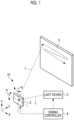
- Fig. 1 schematically shows an optical scanning device 10 according to an embodiment.
- the optical scanning device 10 includes a micromirror device (hereinafter, referred to as micromirror device (MMD)) 2, a light source 3, and a driving controller 4.
- MMD micromirror device
- the optical scanning device 10 optically scans a surface to be scanned 5 by reflecting a light beam L emitted from the light source 3 by the MMD 2 under the control of the driving controller 4.
- the surface to be scanned 5 is, for example, a screen.
- the MMD 2 is a piezoelectric biaxial drive type micromirror device capable of allowing a mirror portion 20 (see Fig. 3 ) to swing around a first axis a 1 and a second axis a 2 orthogonal to the first axis a 1 .
- the direction parallel to the first axis a 1 is referred to as an X direction
- the direction parallel to the second axis a 2 is a Y direction
- the direction orthogonal to the first axis a 1 and the second axis a 2 is referred to as a Z direction.
- the light source 3 is a laser device that emits, for example, laser light as the light beam L. It is preferable that the light source 3 emits the light beam L perpendicularly to a reflecting surface 20A (see Fig. 3 ) included in the mirror portion 20 in a state where the mirror portion 20 of the MMD 2 is stationary.
- the driving controller 4 outputs a driving signal to the light source 3 and the MMD 2 based on optical scanning information.
- the light source 3 generates the light beam L based on the input driving signal and emits the light beam L to the MMD 2.
- the MMD 2 allows the mirror portion 20 to swing around the first axis a 1 and the second axis a 2 based on the input driving signal.
- the driving controller 4 allows the mirror portion 20 to resonate around the first axis a 1 and the second axis a 2 , so that the surface to be scanned 5 is scanned with the light beam L reflected by the mirror portion 20 such that a Lissajous waveform is drawn.
- This optical scanning method is called a Lissajous scanning method.
- the optical scanning device 10 is applied to, for example, a Lissajous scanning type laser display.
- the optical scanning device 10 can be applied to a laser scanning display such as augmented reality (AR) glass or virtual reality (VR) glass.
- AR augmented reality
- VR virtual reality
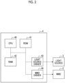
- Fig. 2 shows an example of a hardware configuration of the driving controller 4.
- the driving controller 4 has a central processing unit (CPU) 40, a read only memory (ROM) 41, a random access memory (RAM) 42, a light source driver 43, and an MMD driver 44.
- the CPU 40 is an arithmetic unit that realizes the entire function of the driving controller 4 by reading out a program and data from a storage device such as the ROM 41 into the RAM 42 and executing processing.
- the CPU 40 is an example of a "processor" according to the technique of the present disclosure.
- the ROM 41 is a non-volatile storage device and stores a program for the CPU 40 to execute processing and data such as the optical scanning information described above.
- the RAM 42 is a volatile storage device that temporarily holds a program and data.
- the light source driver 43 is an electric circuit that outputs a driving signal to the light source 3 under the control of the CPU 40.
- the driving signal is a driving voltage for controlling the irradiation timing and the irradiation intensity of the light source 3.
- the MMD driver 44 is an electric circuit that outputs a driving signal to the MMD 2 under the control of the CPU 40.
- the driving signal is a driving voltage for controlling the timing, cycle, and deflection angle for allowing the mirror portion 20 of the MMD 2 to swing.
- the CPU 40 controls the light source driver 43 and the MMD driver 44 based on the optical scanning information.
- the optical scanning information is information including the scanning pattern of the light beam L with which the surface to be scanned 5 is scanned and the light emission timing of the light source 3.
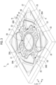
- Fig. 3 is an external perspective view of the MMD 2.
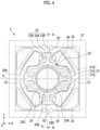
- Fig. 4 is a plan view of the MMD 2 as viewed from the light incident side.
- Fig. 5 is a cross-sectional view taken along the line A-A in Fig. 4 .
- the MMD 2 has the mirror portion 20, a pair of first support portions 21, a pair of movable frames 22, a pair of second support portions 23, a pair of first actuators 24, a pair of second actuators 25, a pair of first connecting portions 26A, a pair of second connecting portions 26B, and a fixed frame 27.
- the MMD 2 is a so-called MEMS scanner.
- the mirror portion 20 has a reflecting surface 20A for reflecting incident light.
- the reflecting surface 20A is formed of a metal thin film such as gold (Au) and aluminum (Al) provided on one surface of the mirror portion 20.
- the shape of the reflecting surface 20A is, for example, circular with the intersection of the first axis a 1 and the second axis a 2 as the center.
- the first axis a 1 and the second axis a 2 exist in a plane including the reflecting surface 20A in a case where the mirror portion 20 is stationary.
- the planar shape of the MMD 2 is rectangular, line-symmetrical with respect to the first axis a 1 , and line-symmetrical with respect to the second axis a 2 .
- the pair of first support portions 21 are disposed at positions facing each other across the second axis a 2 , and have a shape that is line-symmetrical with respect to the second axis a 2 .
- each of the first support portions 21 has a shape that is line-symmetrical with respect to the first axis a 1 .
- the first support portion 21 is connected to the mirror portion 20 on the first axis a 1 , and swingably supports the mirror portion 20 around the first axis a 1 .
- the pair of movable frames 22 are disposed at positions facing each other across the first axis a 1 , and have a shape that is line-symmetrical with respect to the first axis a 1 .
- Each of the movable frames 22 has a shape that is line-symmetrical with respect to the second axis a 2 .
- each of the movable frames 22 is curved along the outer periphery of the mirror portion 20. Both ends of the movable frame 22 are connected to the first support portion 21.
- the first support portion 21 and the movable frame 22 are connected to each other to surround the mirror portion 20.
- the mirror portion 20, the first support portion 21, and the movable frame 22 constitute the movable portion 60.
- the pair of second support portions 23 are disposed at positions facing each other across the first axis a 1 , and have a shape that is line-symmetrical with respect to the first axis a 1 .
- Each of the second support portions 23 has a shape that is line-symmetrical with respect to the second axis a 2 .
- the second support portion 23 is connected to the movable frame 22 on the second axis a 2 , and swingably supports the movable portion 60 having the mirror portion 20 around the second axis a 2 .
- both ends of the second support portion 23 are connected to the first actuator 24.
- the pair of first actuators 24 are disposed at positions facing each other across the second axis a 2 , and have a shape that is line-symmetrical with respect to the second axis a 2 .
- each of the first actuators 24 has a shape that is line-symmetrical with respect to the first axis a 1 .
- the first actuator 24 is formed along the outer periphery of the movable frame 22 and the first support portion 21.
- the first actuator 24 is a piezoelectric drive type actuator comprising a piezoelectric element.
- the first actuator 24 is divided in the vicinity of the first axis a 1 , the first actuator 24 is electrically connected by a wiring line (not shown) via the first axis a 1 .
- the second support portion 23 and the first actuator 24 are connected to each other to surround the movable portion 60.
- the pair of second actuators 25 are disposed at positions facing each other across the first axis a 1 , and have a shape that is line-symmetrical with respect to the first axis a 1 .
- each of the second actuators 25 has a shape that is line-symmetrical with respect to the second axis a 2 .
- the second actuator 25 is formed along the outer periphery of the first actuator 24 and the second support portion 23.
- the second actuator 25 is a piezoelectric drive type actuator comprising a piezoelectric element.
- the pair of first connecting portions 26A are disposed at positions facing each other across the second axis a 2 , and have a shape that is line-symmetrical with respect to the second axis a 2 .
- each of the first connecting portions 26A has a shape that is line-symmetrical with respect to the first axis a 1 .
- the first connecting portion 26A is disposed along the first axis a 1 , and connects the first actuator 24 and the second actuator 25 on the first axis a 1 .
- the pair of second connecting portions 26B are disposed at positions facing each other across the first axis a 1 , and have a shape that is line-symmetrical with respect to the first axis a 1 .
- each of the second connecting portions 26B has a shape that is line-symmetrical with respect to the second axis a 2 .
- the second connecting portion 26B is disposed along the second axis a 2 , and connects the second actuator 25 and the fixed frame 27 on the second axis a 2 .
- the second actuator 25 and the second connecting portion 26B are connected to each other to surround the movable portion 60 and the first actuator 24.
- the first actuator 24 and the second actuator 25 constitute a driving portion surrounding the movable portion 60.
- the fixed frame 27 is a frame-shaped member having a rectangular outer shape, and has a shape that is line-symmetrical with respect to each of the first axis a 1 and the second axis a 2 .
- the fixed frame 27 surrounds the outer periphery of the second actuator 25 and the second connecting portion 26B. That is, the fixed frame 27 surrounds the driving portion.
- the first actuator 24 and the second actuator 25 are piezoelectric actuators each having a piezoelectric element.
- the pair of first actuators 24 allow the movable portion 60 to swing around the second axis a 2 by applying rotational torque around the second axis a 2 to the mirror portion 20 and the movable frame 22.
- the pair of second actuators 25 allow the mirror portion 20 to swing around the first axis a 1 by applying rotational torque around the first axis a 1 to the mirror portion 20, the movable frame 22, and the first actuator 24.
- the first support portion 21 is composed of a swing shaft 21A and a pair of coupling portions 21B.
- the swing shaft 21A is a so-called torsion bar stretched along the first axis a 1 .
- One end of the swing shaft 21A is connected to the mirror portion 20, and the other end thereof is connected to the coupling portion 21B.
- a spatial gap G1 between the first support portion 21 and the driving portion.
- the pair of coupling portions 21B are disposed at positions facing each other across the first axis a 1 , and have a shape that is line-symmetrical with respect to the first axis a 1 .
- One end of the coupling portion 21B is connected to the swing shaft 21A, and the other end thereof is connected to the movable frame 22.
- the coupling portion 21B has a folded structure. Since the coupling portion 21B has elasticity due to the folded structure, the internal stress applied to the swing shaft 21A is relaxed in a case where the mirror portion 20 swings around the first axis a 1 .
- the second support portion 23 is composed of a swing shaft 23A and a pair of coupling portions 23B.
- the swing shaft 23A is a so-called torsion bar stretched along the second axis a 2 .
- One end of the swing shaft 23A is connected to the movable frame 22, and the other end thereof is connected to the coupling portion 23B.
- the pair of coupling portions 23B are disposed at positions facing each other across the second axis a 2 , and have a shape that is line-symmetrical with respect to the second axis a 2 .
- One end of the coupling portion 23B is connected to the swing shaft 23A, and the other end thereof is connected to the first actuator 24.
- the coupling portion 23B has a folded structure. Since the coupling portion 23B has elasticity due to the folded structure, the internal stress applied to the swing shaft 23A is relaxed in a case where the mirror portion 20 swings around the second axis a 2 .
- a plurality of slits 20B and 20C are formed on the outside of the reflecting surface 20A along the outer periphery of the reflecting surface 20A.
- the plurality of slits 20B and 20C are disposed at positions that are line-symmetrical with respect to the first axis a 1 and the second axis a 2 , respectively.
- the slit 20B has an effect of suppressing distortion generated on the reflecting surface 20A due to the swing of the mirror portion 20.
- Figs. 3 and 4 the wiring line and the electrode pad for giving the driving signal to the first actuator 24 and the second actuator 25 are not shown.
- a plurality of the electrode pads are provided on the fixed frame 27.
- the MMD 2 is formed, for example, by performing an etching treatment on a silicon on insulator (SOI) substrate 30.
- SOI substrate 30 is a substrate in which a silicon oxide layer 32 is provided on a first silicon active layer 31 made of single crystal silicon, and a second silicon active layer 33 made of single crystal silicon is provided on the silicon oxide layer 32.
- the mirror portion 20, the first support portion 21, the movable frame 22, the second support portion 23, the first actuator 24, the second actuator 25, the first connecting portion 26A, and the second connecting portion 26B are formed of the second silicon active layer 33 remaining by removing the first silicon active layer 31 and the silicon oxide layer 32 from the SOI substrate 30 by an etching treatment.
- the second silicon active layer 33 functions as an elastic portion having elasticity.
- the fixed frame 27 is formed of three layers of the first silicon active layer 31, the silicon oxide layer 32, and the second silicon active layer 33.
- the first actuator 24 includes a piezoelectric element (not shown) formed on the second silicon active layer 33.
- the piezoelectric element has a laminated structure in which a lower electrode, a piezoelectric film, and an upper electrode are sequentially laminated on the second silicon active layer 33.
- the second actuator 25 has the same configuration as the first actuator 24.
- the upper electrode and the lower electrode are formed of, for example, gold (Au) or platinum (Pt).
- the piezoelectric film is formed of, for example, lead zirconate titanate (PZT), which is a piezoelectric material.
- PZT lead zirconate titanate
- a driving voltage is applied to the upper electrode from the driving controller 4.
- the lower electrode is connected to the driving controller 4 via the wiring line and the electrode pad, and a reference potential (for example, a ground potential) is applied thereto.
- the piezoelectric film exerts a so-called inverse piezoelectric effect.
- the piezoelectric film exerts an inverse piezoelectric effect by applying a driving voltage from the driving controller 4 to the upper electrode, and displaces the first actuator 24 and the second actuator 25.
- Fig. 6 shows an example in which one piezoelectric film of the pair of second actuators 25 is extended and the other piezoelectric film is contracted, thereby generating rotational torque around the first axis a 1 in the second actuator 25.
- one of the pair of second actuators 25 and the other are displaced in opposite directions to each other, whereby the mirror portion 20 rotates around the first axis a 1 .
- Fig. 6 shows an example in which the second actuator 25 is driven in an anti-phase resonance mode (hereinafter, referred to as an anti-phase rotation mode) in which the displacement direction of the pair of second actuators 25 and the rotation direction of the mirror portion 20 are opposite to each other.
- an in-phase resonance mode in which the displacement direction of the pair of second actuators 25 and the rotation direction of the mirror portion 20 are the same direction is called an in-phase rotation mode.
- the second actuator 25 is driven in the anti-phase rotation mode.
- a deflection angle ⁇ of the mirror portion 20 around the first axis a 1 is controlled by the driving signal (hereinafter, referred to as a first driving signal) given to the second actuator 25 by the driving controller 4.
- the first driving signal is, for example, a sinusoidal AC voltage.
- the first driving signal includes a driving voltage waveform V 1A (t) applied to one of the pair of second actuators 25 and a driving voltage waveform V 1B (t) applied to the other.
- the driving voltage waveform V 1A (t) and the driving voltage waveform V 1B (t) are in an anti-phase with each other (that is, the phase difference is 180°).
- the deflection angle ⁇ of the mirror portion 20 around the first axis a 1 corresponds to an angle at which the normal line N of the reflecting surface 20A is inclined with respect to the Z direction in the YZ plane.
- the deflection angle ⁇ is also referred to as a rotation angle ⁇ .
- the first actuator 24 is driven in an anti-phase resonance mode in the same manner as the second actuator 25.
- a deflection angle of the mirror portion 20 around the second axis a 2 is controlled by the driving signal (hereinafter, referred to as a second driving signal) given to the first actuator 24 by the driving controller 4.
- the second driving signal is, for example, a sinusoidal AC voltage.
- the second driving signal includes a driving voltage waveform V 2A (t) applied to one of the pair of second actuators 25 and a driving voltage waveform V 2B (t) applied to the other.
- the driving voltage waveform V 2A (t) and the driving voltage waveform V 2B (t) are in an anti-phase with each other (that is, the phase difference is 180°).
- Figs. 7A and 7B show examples of the first driving signal and the second driving signal.
- Fig. 7A shows the driving voltage waveforms V 1A (t) and V 1B (t) included in the first driving signal.
- Fig. 7B shows the driving voltage waveforms V 2A (t) and V 2B (t) included in the second driving signal.
- V 1A (t) and V 1B (t) are represented as follows, respectively.
- V 1 A t V off 1 + V 1 sin 2 ⁇ f d 1 t
- V 1 B t V off 1 + V 1 sin 2 ⁇ f d 1 t + ⁇
- V 1 is the amplitude voltage.
- V off1 is the bias voltage.
- f d1 is the driving frequency (hereinafter, referred to as the first driving frequency).
- t is time.
- the mirror portion 20 swings around the first axis a 1 at the first driving frequency f d1 .
- V 2A (t) and V 2B (t) are represented as follows, respectively.
- V 2 A t V off 2 + V 2 sin 2 ⁇ f d 2 t + ⁇
- V 2 B t V off 2 + V 2 sin 2 ⁇ f d 2 t + ⁇ + ⁇
- V 2 is the amplitude voltage.
- V off2 is the bias voltage.
- f d2 is the driving frequency (hereinafter, referred to as the second driving frequency).
- t is time.
- ⁇ is the phase difference between the driving voltage waveforms V 1A (t) and V 1B (t) and the driving voltage waveforms V 2A (t) and V 2B (t).
- the movable portion 60 including the mirror portion 20 swings around the second axis a 2 at the second driving frequency f d2 .
- the first driving frequency f d1 is set so as to match the resonance frequency around the first axis a 1 of the mirror portion 20.
- the second driving frequency f d2 is set so as to match the resonance frequency around the second axis a 2 of the mirror portion 20.
- the first driving frequency f d1 is larger than the second driving frequency f d2 .
- the centrifugal force acting in a case where the movable portion 60 swings around the second axis a 2 serves to assist the swing of the mirror portion 20 around the first axis a 1 .
- the potential energy by the centrifugal force affects the total amount of elastic energy and kinetic energy stored in a case where the mirror portion 20 swings.
- a spring constant in the swing of the mirror portion 20 changes and a crosstalk between axes occurs, so that the resonance frequency shifts.
- the present applicant found that in a case where the displacement of the second support portion 23 satisfies a predetermined condition in a state where the mirror portion 20 rotates around the first axis a 1 and an absolute value of the rotation angle ⁇ is larger than 0 degrees, the shift of the resonance frequency by the crosstalk between axes is suppressed.
- a displacement amount of a portion of the movable portion 60 other than the mirror portion 20 increases.
- the total amount of elastic energy and kinetic energy in the entire MMD 2 is increased.
- the influence of the potential energy by the centrifugal force on the total energy is relatively reduced, and the shift of the resonance frequency by the crosstalk between axes is suppressed.
- Fig. 8 is a diagram schematically showing displacement of the second support portion 23 in a case where the mirror portion 20 rotates around the first axis a 1 .
- A) of Fig. 8 shows a state where the mirror portion 20 is stationary and the rotation angle ⁇ is 0 degrees.
- (B) of Fig. 8 shows a state where the mirror portion 20 rotates around the first axis a 1 and the absolute value of the rotation angle ⁇ is larger than 0 degrees.
- Fig. 8 shows a cross-sectional view of the MMD 2 cut along a plane orthogonal to the first axis a 1 and including the second axis a 2 .
- a straight line ⁇ and an intersection C shown in (B) of Fig. 8 are included in the cross section of the MMD 2.
- the straight line ⁇ is a straight line located on the surface of the second support portion 23 and including each end point of the second support portion 23.
- the intersection C is a point where the straight line ⁇ intersects the second axis a 2 .
- the total length of the second support portion 23 in the direction of the second axis a 2 in the stationary state is denoted by Lb1.
- the distance from an end part of the second support portion 23 on the mirror portion 20 side in the stationary state to the intersection C is denoted by A.
- the present applicant prepared a plurality of samples having different distances A for the MMD 2, and measured the shift amount of the resonance frequency by the crosstalk between axes by driving each sample. Specifically, a resonance frequency around the first axis a 1 in a case where each sample is driven one-dimensionally around the first axis a 1 (hereinafter, referred to as a first resonance frequency fr1) and a resonance frequency around the first axis a 1 in a case where each sample is driven two-dimensionally around the first axis a 1 and the second axis a 2 (hereinafter, referred to as a second resonance frequency fr2) were measured. Then, a shift amount ⁇ fr of the resonance frequency by the crosstalk between axes was obtained by calculating a difference between the first resonance frequency fr1 and the second resonance frequency fr2.
- a resonance frequency around the first axis a 1 in a case where each sample is driven one-dimensionally around the first axis a 1 hereinafter, referred to as a first resonance
- Figs. 9 and 10 show parameters relating to the width, length, and the like of the components of the sample used in the experiment.
- Fig. 11 is a diagram showing specific setting values of the parameters.
- the diameter of the mirror portion 20 was 1.5 mm
- the thickness of the SOI substrate 30 was 430 ⁇ m
- the thickness of the second silicon active layer 33 was 60 ⁇ m
- the thickness of the silicon oxide layer 32 was 40 ⁇ m.
- the length of one side of the fixed frame 27 was 5.2 mm.
- the present applicant used Xac2 and Yac2 as variables among the parameters shown in Fig. 11 . That is, the present applicant prepared a plurality of samples having different distances A by changing the lengths of Xac2 and Yac2 for each sample.
- the present applicant prepared samples for an MMD 2A in which the shape and the like of the components are different from those of the MMD 2 according to the above embodiment.
- Fig. 12 shows the configuration of the MMD 2A according to Modification Example not covered by the subject-matter of the claims.
- the components having the same functions as those of the MMD 2 according to the above embodiment are designated by the same reference numerals.
- a connecting portion 26 is provided instead of the first connecting portion 26A and the second connecting portion 26B.
- the connecting portion 26 is provided on the first axis a 1 , and connects the first actuator 24 to the second actuator 25 and connects the second actuator 25 to the fixed frame 27.
- Figs. 13 to 15 show parameters relating to the width, length, and the like of the components of the MMD 2A.
- Fig. 16 is a diagram showing specific setting values of the parameters.
- the diameter of the mirror portion 20 was 1.5 mm
- the thickness of the SOI substrate 30 was 350 ⁇ m
- the thickness of the second silicon active layer 33 is 60 ⁇ m
- the thickness of the silicon oxide layer 32 was 65 ⁇ m.
- the length of one side of the fixed frame 27 was 5.2 mm.
- each sample was driven in a vacuum chamber to measure the first resonance frequency fr1 and the second resonance frequency fr2.
- the driving frequency was swept while irradiating the mirror portion 20 during driving with laser light, and the driving frequency at which a spreading angle of reflected light was maximized was measured as the resonance frequency.
- the deflection angle of the mirror portion 20 was calculated from the spreading angle of the reflected light.
- Fig. 17 shows measurement results of the first resonance frequency fr1 and the second resonance frequency fr2 for each sample.
- Sample number 1 indicates a sample prepared for the MMD 2A according to Modification Example and is not covered by the subject-matter of the claims.
- Sample numbers 2 to 9 indicate samples prepared for the MMD 2 according to the embodiment. Sample numbers 2 to 9 have different lengths of Xac2 and Yac2. Sample numbers 2 to 4 are not covered by the subject-matter of the claims.
- the first resonance frequency fr1 is a resonance frequency during one-dimensional driving in a case where the deflection angle of the mirror portion 20 around the first axis a 1 is ⁇ 1.25 degrees.
- the second resonance frequency fr2 is a resonance frequency during two-dimensional driving in a case where the deflection angle of the mirror portion 20 around the first axis a 1 is ⁇ 1.25 degrees and the deflection angle of the mirror portion 20 around the second axis a 2 is ⁇ 11.5 degrees.
- the shift amount ⁇ fr of the resonance frequency is a value obtained by subtracting the first resonance frequency fr1 from the second resonance frequency fr2.
- the distance A was measured for each sample using a laser Doppler vibrometer. Then, using the measured distance A, a ratio A/Lb1 of the distance A to the total length Lb1 of the second support portion 23 was calculated.
- an appropriate value of the deflection angle of the mirror portion 20 around each axis during the two-dimensional driving is ⁇ 17 degrees around the first axis a 1 and ⁇ 11.5 degrees around the second axis a 2 . Therefore, for each sample, it was determined whether or not the two-dimensional driving was possible stably for 60 seconds or longer while maintaining the deflection angle at an appropriate value.
- the term "OK” indicates that the stable two-dimensional driving for 60 seconds or longer was possible.
- the term “NG” indicates that the stable two-dimensional driving for 60 seconds or longer was not possible.
- the power consumption of each sample was measured using a current probe in a state where the sample was resonated by the one-dimensional driving around the first axis a 1 .
- the deflection angle of the mirror portion 20 around the first axis a 1 was ⁇ 17 degrees.
- Fig. 17 is a graph showing dependence of the shift amount ⁇ fr of the resonance frequency on the ratio A/Lb1.
- Fig. 19 is a graph showing dependence of power consumption on the ratio A/Lb1.
- Low power consumption is desirable for a general laser display application.
- the power consumption during the one-dimensional driving is 80 mW or less
- a certain degree of superiority as a laser display application can be secured. Therefore, it can be seen that in a case where the ratio A/Lb1 is 6/5 or less (1.2 or less), the power consumption is 80 mW or less, and a certain degree of superiority can be secured from the viewpoint of the power consumption.
- the ratio A/Lb1 satisfies a relationship of 2/3 ⁇ A/Lb1. Further, it is preferable that the ratio A/Lb1 satisfies a relationship of 2/3 ⁇ A/Lb1 ⁇ 6/5.
- Fig. 20 shows the simulation results.
- (A) to (C) of Fig. 20 show that the lengths of Xac2 and Yac2 are different.
- the intersection C corresponds to a point where the displacement of the second support portion 23 is zero. It can be seen that the position of the intersection C changes (that is, the distance A changes) according to the lengths of Xac2 and Yac2. Also in the simulation, it was confirmed that the larger the ratio A/Lb1, the smaller the shift amount ⁇ fr of the resonance frequency.
- the processing unit of the driving controller 4 may be composed of one processor or may be composed of a combination of two or more processors of the same type or different types.
- the processor includes, for example, a CPU, a programmable logic device (PLD), or a dedicated electric circuit.
- the CPU is a general-purpose processor that executes software (program) to function as various processing units.
- the PLD is a processor such as a field programmable gate array (FPGA) whose circuit configuration can be changed after manufacture.
- the dedicated electric circuit is a processor that has a dedicated circuit configuration designed to perform a specific process, such as an application specific integrated circuit (ASIC).
- ASIC application specific integrated circuit
Landscapes
- Physics & Mathematics (AREA)
- General Physics & Mathematics (AREA)
- Optics & Photonics (AREA)
- Mechanical Light Control Or Optical Switches (AREA)
- Mechanical Optical Scanning Systems (AREA)
- Micromachines (AREA)
Claims (6)
- Mikrospiegelvorrichtung (2, 2A), umfassend:einen Spiegelabschnitt (20), auf dem eine reflektierende Fläche (20A) zum Reflektieren von einfallendem Licht gebildet ist;einen ersten Lagerabschnitt (21), der mit dem Spiegelabschnitt (20) auf einer ersten Achse (a1), die sich in einer Ebene, die die reflektierende Fläche (20A) des Spiegelabschnitts (20) in einem stationären Zustand enthält, befindet, verbunden ist und der den Spiegelabschnitt (20) um die erste Achse (a1) schwenkbar lagert;ein Paar beweglicher Rahmen (22), die mit dem ersten Lagerabschnitt (21) verbunden sind und über die erste Achse (a1) einander zugewandt sind;einen zweiten Lagerabschnitt (23), der mit dem Paar beweglicher Rahmen (22) auf einer zweiten Achse (a2), die sich in der Ebene, die die reflektierende Fläche (20A) des Spiegelabschnitts (20) in dem stationären Zustand enthält, befindet und zu der ersten Achse (a1) senkrecht ist, verbunden ist und der einen beweglichen Abschnitt (60), der den Spiegelabschnitt (20), den ersten Lagerabschnitt (21) und das Paar von beweglichen Rahmen (22) enthält, um die zweite Achse (a2) schwenkbar lagert;einen Antriebsabschnitt (24, 25), der den beweglichen Abschnitt (60) umgibt und einen Spalt (G2) mit dem zweiten Lagerabschnitt (23) auf der zweiten Achse (a2) aufweist;wobei der zweite Lagerabschnitt (23) eine Schwenkwelle (23A) und ein Paar Kupplungsabschnitte (23B) aufweist, wobei das Paar Kupplungsabschnitte (23B) den zweiten Lagerabschnitt (23) und den Antriebsabschnitt (24, 25) koppelt; und einen festen Rahmen (27), der mit dem Antriebsabschnitt (24, 25) verbunden ist und den Antriebsabschnitt (24, 25) umgibt,dadurch gekennzeichnet, dass in einem Zustand, in dem sich der Spiegelabschnitt (20) um die erste Achse (a1) dreht und ein Absolutwert eines Drehwinkels größer als 0 Grad ist,unter der Annahme, dass in einer Ebene, die senkrecht zu der ersten Achse (a1) steht und die zweite Achse (a2) enthält, ein Abstand zwischen einem Schnittpunkt (C) zwischen der zweiten Achse (a2) und einer geraden Linie (α), die sich auf einer Oberfläche des zweiten Lagerabschnitts (23) befindet und jeden Endpunkt des zweiten Lagerabschnitts (23) und einen Endteil des zweiten Lagerabschnitts (23) auf einer Seite eines Spiegelabschnitts (20) in dem stationären Zustand enthält, mit A bezeichnet wird und eine Gesamtlänge des zweiten Lagerabschnitts (23) in einer Richtung der zweiten Achse (a2) mit L bezeichnet wird, eine Beziehung von 2/3 < A/L erfüllt ist.
- Mikrospiegelvorrichtung (2, 2A) nach Anspruch 1,
wobei der Antriebsabschnitt (24, 25) ein piezoelektrisches Element aufweist. - Mikrospiegelvorrichtung (2, 2A) nach Anspruch 1,
wobei der Antriebsabschnitt (24, 25) enthält:ein Paar erster Aktuatoren (24), die über die zweite Achse (a2) einander zugewandt sind und ein piezoelektrisches Element aufweisen, undein Paar zweiter Aktuatoren (25), die das Paar erster Aktuatoren (24) umgeben, über die erste Achse (a1) einander zugewandt sind und ein piezoelektrisches Element aufweisen. - Mikrospiegelvorrichtung (2, 2A) nach Anspruch 3,wobei das Paar zweiter Aktuatoren (25) es dem Spiegelabschnitt (20) ermöglicht, um die erste Achse (a1) zu schwingen, unddas Paar erster Aktuatoren (24) es dem beweglichen Abschnitt (60) ermöglicht, um die zweite Achse (a2) zu schwingen.
- Mikrospiegelvorrichtung (2, 2A) nach einem der Ansprüche 1 bis 4,
wobei der Abstand A und die Gesamtlänge L eine Beziehung von 2/3 < A/L < 6/5 erfüllen. - Optische Abtastvorrichtung (10), umfassend:die Mikrospiegelvorrichtung (2, 2A) nach einem der Ansprüche 1 bis 4; undeinen Prozessor, der so konfiguriert ist, dass er den Antriebsabschnitt (24, 25) antreibt,wobei der Prozessor so konfiguriert ist, dass er ein Antriebssignal an den Ansteuerabschnitt (24, 25) bereitstellt, um den Spiegelabschnitt (20) um die erste Achse (a1) und die zweite Achse (a2) zu schwingen.
Applications Claiming Priority (1)
| Application Number | Priority Date | Filing Date | Title |
|---|---|---|---|
| JP2021146275A JP7693475B2 (ja) | 2021-09-08 | 2021-09-08 | マイクロミラーデバイス及び光走査装置 |
Publications (2)
| Publication Number | Publication Date |
|---|---|
| EP4148481A1 EP4148481A1 (de) | 2023-03-15 |
| EP4148481B1 true EP4148481B1 (de) | 2025-06-18 |
Family
ID=83059383
Family Applications (1)
| Application Number | Title | Priority Date | Filing Date |
|---|---|---|---|
| EP22192004.4A Active EP4148481B1 (de) | 2021-09-08 | 2022-08-24 | Mikrospiegelvorrichtung und optische abtastvorrichtung |
Country Status (4)
| Country | Link |
|---|---|
| US (1) | US12386172B2 (de) |
| EP (1) | EP4148481B1 (de) |
| JP (1) | JP7693475B2 (de) |
| CN (1) | CN115774332A (de) |
Families Citing this family (1)
| Publication number | Priority date | Publication date | Assignee | Title |
|---|---|---|---|---|
| JPWO2024062856A1 (de) * | 2022-09-20 | 2024-03-28 |
Citations (1)
| Publication number | Priority date | Publication date | Assignee | Title |
|---|---|---|---|---|
| EP4249985A1 (de) * | 2022-03-24 | 2023-09-27 | FUJIFILM Corporation | Mikrospiegelvorrichtung und optische abtastvorrichtung |
Family Cites Families (8)
| Publication number | Priority date | Publication date | Assignee | Title |
|---|---|---|---|---|
| US7630112B2 (en) * | 2007-05-15 | 2009-12-08 | Konica Minolta Opto, Inc. | Image display apparatus |
| US7880948B2 (en) * | 2007-09-26 | 2011-02-01 | Konica Minolta Opto, Inc. | Scanning projection device |
| EP2317365A1 (de) | 2008-08-22 | 2011-05-04 | Konica Minolta Opto, Inc. | Antriebsvorrichtung |
| WO2010035759A1 (ja) * | 2008-09-25 | 2010-04-01 | コニカミノルタオプト株式会社 | 光スキャナ |
| JP6581002B2 (ja) | 2016-01-25 | 2019-09-25 | スタンレー電気株式会社 | 前照灯装置 |
| DE102016208924A1 (de) * | 2016-05-24 | 2017-11-30 | Robert Bosch Gmbh | Mikromechanisches Bauteil und Verfahren zum Verstellen eines verstellbaren Teils gleichzeitig um zwei zueinander geneigte Drehachsen |
| JP7132481B2 (ja) * | 2018-02-23 | 2022-09-07 | ミツミ電機株式会社 | アクチュエータ及び光走査装置 |
| EP3872556A4 (de) * | 2018-10-25 | 2021-12-08 | FUJIFILM Corporation | Mikrospiegelvorrichtung und verfahren zur ansteuerung einer mikrospiegelvorrichtung |
-
2021
- 2021-09-08 JP JP2021146275A patent/JP7693475B2/ja active Active
-
2022
- 2022-08-24 EP EP22192004.4A patent/EP4148481B1/de active Active
- 2022-08-30 CN CN202211045903.2A patent/CN115774332A/zh active Pending
- 2022-09-02 US US17/901,969 patent/US12386172B2/en active Active
Patent Citations (1)
| Publication number | Priority date | Publication date | Assignee | Title |
|---|---|---|---|---|
| EP4249985A1 (de) * | 2022-03-24 | 2023-09-27 | FUJIFILM Corporation | Mikrospiegelvorrichtung und optische abtastvorrichtung |
Also Published As
| Publication number | Publication date |
|---|---|
| JP2023039221A (ja) | 2023-03-20 |
| US20230073166A1 (en) | 2023-03-09 |
| EP4148481A1 (de) | 2023-03-15 |
| US12386172B2 (en) | 2025-08-12 |
| CN115774332A (zh) | 2023-03-10 |
| JP7693475B2 (ja) | 2025-06-17 |
Similar Documents
| Publication | Publication Date | Title |
|---|---|---|
| EP4148482B1 (de) | Mikrospiegelvorrichtung und optische abtastvorrichtung | |
| EP4209824B1 (de) | Mikrospiegelvorrichtung und optisches abtastgerät | |
| EP4075183B1 (de) | Optische abtastvorrichtung | |
| US12411338B2 (en) | Micromirror device and optical scanning device | |
| EP4249985B1 (de) | Mikrospiegelvorrichtung und optische abtastvorrichtung | |
| US12379588B2 (en) | Optical scanning device and method of driving micromirror device | |
| EP4148481B1 (de) | Mikrospiegelvorrichtung und optische abtastvorrichtung | |
| US12517346B2 (en) | Optical scanning device and method of driving micromirror device | |
| US20250216669A1 (en) | Micromirror device and optical scanning device | |
| US20250208405A1 (en) | Micromirror device and optical scanning device | |
| CN121039549A (zh) | 反射镜装置及光扫描装置 | |
| WO2025037515A1 (ja) | ミラー装置及び光走査装置 |
Legal Events
| Date | Code | Title | Description |
|---|---|---|---|
| PUAI | Public reference made under article 153(3) epc to a published international application that has entered the european phase |
Free format text: ORIGINAL CODE: 0009012 |
|
| STAA | Information on the status of an ep patent application or granted ep patent |
Free format text: STATUS: THE APPLICATION HAS BEEN PUBLISHED |
|
| AK | Designated contracting states |
Kind code of ref document: A1 Designated state(s): AL AT BE BG CH CY CZ DE DK EE ES FI FR GB GR HR HU IE IS IT LI LT LU LV MC MK MT NL NO PL PT RO RS SE SI SK SM TR |
|
| STAA | Information on the status of an ep patent application or granted ep patent |
Free format text: STATUS: REQUEST FOR EXAMINATION WAS MADE |
|
| 17P | Request for examination filed |
Effective date: 20230620 |
|
| RBV | Designated contracting states (corrected) |
Designated state(s): AL AT BE BG CH CY CZ DE DK EE ES FI FR GB GR HR HU IE IS IT LI LT LU LV MC MK MT NL NO PL PT RO RS SE SI SK SM TR |
|
| STAA | Information on the status of an ep patent application or granted ep patent |
Free format text: STATUS: EXAMINATION IS IN PROGRESS |
|
| 17Q | First examination report despatched |
Effective date: 20250130 |
|
| GRAP | Despatch of communication of intention to grant a patent |
Free format text: ORIGINAL CODE: EPIDOSNIGR1 |
|
| STAA | Information on the status of an ep patent application or granted ep patent |
Free format text: STATUS: GRANT OF PATENT IS INTENDED |
|
| INTG | Intention to grant announced |
Effective date: 20250402 |
|
| GRAS | Grant fee paid |
Free format text: ORIGINAL CODE: EPIDOSNIGR3 |
|
| GRAA | (expected) grant |
Free format text: ORIGINAL CODE: 0009210 |
|
| STAA | Information on the status of an ep patent application or granted ep patent |
Free format text: STATUS: THE PATENT HAS BEEN GRANTED |
|
| AK | Designated contracting states |
Kind code of ref document: B1 Designated state(s): AL AT BE BG CH CY CZ DE DK EE ES FI FR GB GR HR HU IE IS IT LI LT LU LV MC MK MT NL NO PL PT RO RS SE SI SK SM TR |
|
| REG | Reference to a national code |
Ref country code: GB Ref legal event code: FG4D |
|
| REG | Reference to a national code |
Ref country code: CH Ref legal event code: EP |
|
| REG | Reference to a national code |
Ref country code: DE Ref legal event code: R096 Ref document number: 602022016007 Country of ref document: DE |
|
| REG | Reference to a national code |
Ref country code: CH Ref legal event code: EP |
|
| REG | Reference to a national code |
Ref country code: IE Ref legal event code: FG4D |
|
| PG25 | Lapsed in a contracting state [announced via postgrant information from national office to epo] |
Ref country code: FI Free format text: LAPSE BECAUSE OF FAILURE TO SUBMIT A TRANSLATION OF THE DESCRIPTION OR TO PAY THE FEE WITHIN THE PRESCRIBED TIME-LIMIT Effective date: 20250618 |
|
| PGFP | Annual fee paid to national office [announced via postgrant information from national office to epo] |
Ref country code: DE Payment date: 20250716 Year of fee payment: 4 |
|
| REG | Reference to a national code |
Ref country code: LT Ref legal event code: MG9D |
|
| PG25 | Lapsed in a contracting state [announced via postgrant information from national office to epo] |
Ref country code: GR Free format text: LAPSE BECAUSE OF FAILURE TO SUBMIT A TRANSLATION OF THE DESCRIPTION OR TO PAY THE FEE WITHIN THE PRESCRIBED TIME-LIMIT Effective date: 20250919 Ref country code: NO Free format text: LAPSE BECAUSE OF FAILURE TO SUBMIT A TRANSLATION OF THE DESCRIPTION OR TO PAY THE FEE WITHIN THE PRESCRIBED TIME-LIMIT Effective date: 20250918 |
|
| PG25 | Lapsed in a contracting state [announced via postgrant information from national office to epo] |
Ref country code: BG Free format text: LAPSE BECAUSE OF FAILURE TO SUBMIT A TRANSLATION OF THE DESCRIPTION OR TO PAY THE FEE WITHIN THE PRESCRIBED TIME-LIMIT Effective date: 20250618 |
|
| PG25 | Lapsed in a contracting state [announced via postgrant information from national office to epo] |
Ref country code: HR Free format text: LAPSE BECAUSE OF FAILURE TO SUBMIT A TRANSLATION OF THE DESCRIPTION OR TO PAY THE FEE WITHIN THE PRESCRIBED TIME-LIMIT Effective date: 20250618 |
|
| PGFP | Annual fee paid to national office [announced via postgrant information from national office to epo] |
Ref country code: AT Payment date: 20251020 Year of fee payment: 4 |
|
| PG25 | Lapsed in a contracting state [announced via postgrant information from national office to epo] |
Ref country code: RS Free format text: LAPSE BECAUSE OF FAILURE TO SUBMIT A TRANSLATION OF THE DESCRIPTION OR TO PAY THE FEE WITHIN THE PRESCRIBED TIME-LIMIT Effective date: 20250918 |
|
| REG | Reference to a national code |
Ref country code: NL Ref legal event code: MP Effective date: 20250618 |
|
| PG25 | Lapsed in a contracting state [announced via postgrant information from national office to epo] |
Ref country code: LV Free format text: LAPSE BECAUSE OF FAILURE TO SUBMIT A TRANSLATION OF THE DESCRIPTION OR TO PAY THE FEE WITHIN THE PRESCRIBED TIME-LIMIT Effective date: 20250618 |
|
| PG25 | Lapsed in a contracting state [announced via postgrant information from national office to epo] |
Ref country code: NL Free format text: LAPSE BECAUSE OF FAILURE TO SUBMIT A TRANSLATION OF THE DESCRIPTION OR TO PAY THE FEE WITHIN THE PRESCRIBED TIME-LIMIT Effective date: 20250618 |
|
| PG25 | Lapsed in a contracting state [announced via postgrant information from national office to epo] |
Ref country code: PT Free format text: LAPSE BECAUSE OF FAILURE TO SUBMIT A TRANSLATION OF THE DESCRIPTION OR TO PAY THE FEE WITHIN THE PRESCRIBED TIME-LIMIT Effective date: 20251020 |
|
| REG | Reference to a national code |
Ref country code: AT Ref legal event code: MK05 Ref document number: 1804716 Country of ref document: AT Kind code of ref document: T Effective date: 20250618 |
|
| PG25 | Lapsed in a contracting state [announced via postgrant information from national office to epo] |
Ref country code: IS Free format text: LAPSE BECAUSE OF FAILURE TO SUBMIT A TRANSLATION OF THE DESCRIPTION OR TO PAY THE FEE WITHIN THE PRESCRIBED TIME-LIMIT Effective date: 20251018 |
|
| PG25 | Lapsed in a contracting state [announced via postgrant information from national office to epo] |
Ref country code: AT Free format text: LAPSE BECAUSE OF FAILURE TO SUBMIT A TRANSLATION OF THE DESCRIPTION OR TO PAY THE FEE WITHIN THE PRESCRIBED TIME-LIMIT Effective date: 20250618 Ref country code: SM Free format text: LAPSE BECAUSE OF FAILURE TO SUBMIT A TRANSLATION OF THE DESCRIPTION OR TO PAY THE FEE WITHIN THE PRESCRIBED TIME-LIMIT Effective date: 20250618 |
|
| PG25 | Lapsed in a contracting state [announced via postgrant information from national office to epo] |
Ref country code: CZ Free format text: LAPSE BECAUSE OF FAILURE TO SUBMIT A TRANSLATION OF THE DESCRIPTION OR TO PAY THE FEE WITHIN THE PRESCRIBED TIME-LIMIT Effective date: 20250618 |
|
| PG25 | Lapsed in a contracting state [announced via postgrant information from national office to epo] |
Ref country code: PL Free format text: LAPSE BECAUSE OF FAILURE TO SUBMIT A TRANSLATION OF THE DESCRIPTION OR TO PAY THE FEE WITHIN THE PRESCRIBED TIME-LIMIT Effective date: 20250618 |
|
| PG25 | Lapsed in a contracting state [announced via postgrant information from national office to epo] |
Ref country code: EE Free format text: LAPSE BECAUSE OF FAILURE TO SUBMIT A TRANSLATION OF THE DESCRIPTION OR TO PAY THE FEE WITHIN THE PRESCRIBED TIME-LIMIT Effective date: 20250618 |
|
| PG25 | Lapsed in a contracting state [announced via postgrant information from national office to epo] |
Ref country code: SK Free format text: LAPSE BECAUSE OF FAILURE TO SUBMIT A TRANSLATION OF THE DESCRIPTION OR TO PAY THE FEE WITHIN THE PRESCRIBED TIME-LIMIT Effective date: 20250618 |