EP4148436A1 - A system for testing an electronic circuit and corresponding method and computer program product - Google Patents
A system for testing an electronic circuit and corresponding method and computer program product Download PDFInfo
- Publication number
- EP4148436A1 EP4148436A1 EP22192346.9A EP22192346A EP4148436A1 EP 4148436 A1 EP4148436 A1 EP 4148436A1 EP 22192346 A EP22192346 A EP 22192346A EP 4148436 A1 EP4148436 A1 EP 4148436A1
- Authority
- EP
- European Patent Office
- Prior art keywords
- output
- cmd
- test
- signal
- time
- Prior art date
- Legal status (The legal status is an assumption and is not a legal conclusion. Google has not performed a legal analysis and makes no representation as to the accuracy of the status listed.)
- Granted
Links
Images




Classifications
-
- G—PHYSICS
- G01—MEASURING; TESTING
- G01R—MEASURING ELECTRIC VARIABLES; MEASURING MAGNETIC VARIABLES
- G01R31/00—Arrangements for testing electric properties; Arrangements for locating electric faults; Arrangements for electrical testing characterised by what is being tested not provided for elsewhere
- G01R31/28—Testing of electronic circuits, e.g. by signal tracer
- G01R31/282—Testing of electronic circuits specially adapted for particular applications not provided for elsewhere
-
- G—PHYSICS
- G01—MEASURING; TESTING
- G01R—MEASURING ELECTRIC VARIABLES; MEASURING MAGNETIC VARIABLES
- G01R31/00—Arrangements for testing electric properties; Arrangements for locating electric faults; Arrangements for electrical testing characterised by what is being tested not provided for elsewhere
- G01R31/28—Testing of electronic circuits, e.g. by signal tracer
- G01R31/317—Testing of digital circuits
- G01R31/3181—Functional testing
- G01R31/3187—Built-in tests
-
- G—PHYSICS
- G01—MEASURING; TESTING
- G01R—MEASURING ELECTRIC VARIABLES; MEASURING MAGNETIC VARIABLES
- G01R31/00—Arrangements for testing electric properties; Arrangements for locating electric faults; Arrangements for electrical testing characterised by what is being tested not provided for elsewhere
- G01R31/28—Testing of electronic circuits, e.g. by signal tracer
- G01R31/2832—Specific tests of electronic circuits not provided for elsewhere
- G01R31/2834—Automated test systems [ATE]; using microprocessors or computers
-
- G—PHYSICS
- G01—MEASURING; TESTING
- G01R—MEASURING ELECTRIC VARIABLES; MEASURING MAGNETIC VARIABLES
- G01R31/00—Arrangements for testing electric properties; Arrangements for locating electric faults; Arrangements for electrical testing characterised by what is being tested not provided for elsewhere
- G01R31/28—Testing of electronic circuits, e.g. by signal tracer
- G01R31/317—Testing of digital circuits
- G01R31/31724—Test controller, e.g. BIST state machine
Definitions
- Embodiments of the present disclosure relate to techniques for testing electronic circuit, in particular integrated circuits, comprising pre-driver circuits.
- Embodiments of the present disclosure relate in particular to integrated circuits comprising drivers of active loads or capacitive loads and corresponding pre-driver circuits.
- Testing cost is one of the major contributions on the overall manufacturing cost of an electronic circuit, specifically of an integrated circuit.
- output drivers In integrated circuits are for instance used circuit configured to supply a current to a load, for instance, e.g. output drivers, by way of example in transmitting device.
- Such output drivers usually include a pair of switches, e.g. same type MOSFET transistor, arranged in series or totem pole between a voltage supply, to which the so-called pull-up switch is coupled, and a lower voltage such as ground, to which the so-called pull-down switch is coupled.
- the switches have a common node, usually the source of the pull-up switch coupled to the drain of the pull-down switch.
- a load can be represented by an active load or a capacitive load, and can be embodied by a circuit representing the load or a circuit component, e.g. capacitor.
- half bridges where the half bridge is made of two, e.g. N-channel, FET as switches, the low side coupled between ground and phase node, i.e. the common node, and the high side coupled between the battery voltage and phase node.
- the half bridge is made of two, e.g. N-channel, FET as switches, the low side coupled between ground and phase node, i.e. the common node, and the high side coupled between the battery voltage and phase node.
- pre-driver circuits which output is coupled to the control electrode, e.g. gate, of a respective switch to drive such switch with the current and/or dynamic required.
- Testing cost of gate pre-drivers depends on the number of parameters to be tested (high/low output voltage, current limitation/ peak current, rise/fall time. etc.) in order to guarantee the pre-driver functionality and detect possible defectiveness of manufacturing process. For each of these parameters a test is present at an automatic test equipment (ATE).
- ATE automatic test equipment
- FIG 1 it is shown schematically a solution according to the prior art, where with the reference 10 is indicated an electronic circuit 10, in particular an integrated electronic circuit, comprising a gate pre-driver 12, schematized as an operational amplifier-based circuit which is driven by a logic integrated circuit 11. With 20 is indicated an Automated Testing Equipment 20.
- the electronic circuit 10 comprises a voltage supply input terminal VS, which is coupled to the power supply terminal of the pre-driver 12.
- a gate output terminal G of the electronic circuit 10 is, coupled to the output of the pre-driver 12, while a source terminal S is coupled to the other power supply terminal of the pre-driver 12.
- the integrated electronic circuit 10 includes a test command input terminal TMPIN, which is coupled to an input of the integrated circuit logic 11.
- the automatic test equipment 20 which is configure to couple through terminals G, S, TMPIN and to the electronic circuit 10, comprises a load circuit 21, which is embodied by a power FET, but also can be embodied by a capacitive load, coupled by its two terminals between gate terminal G and source terminal S.
- the gate terminal G is coupled to the gate of the power FET.
- the automatic test equipment 20 further comprises a time measurement unit 22 coupled between the same terminals G,S, a voltage power supply 23 coupled between the voltage supply terminal VS and ground GND, a PWM generator 24 coupled to the test command terminal TMPIN.
- the pre-driver 12 is coupled to the load circuit 21 in the automatic test equipment 20, the voltage supply of the pre-driver 12 is supplied by the voltage power supply 23 in the automatic test equipment 20 and the logic 11 receives test command signal SCMD from the external PWM generator 24 in the automatic test equipment through the test command terminal TMPIN.
- Time measurements necessary to tests are performed with an automatic test equipment dedicated instrument, the time measurement unit 22.
- figure 1 is not shown the stage configured to supply a driving signal to a load, in particular a driver circuit, which is driven by the pre-driver 12, in order to better understand the coupling of the pre-driver 12 to the automatic test equipment 21 for test.
- FIG 2 it is shown instead a more detailed view of an implementation of the circuits of figure 1 .
- the IC logic 11 generates a pullup command PU CMD and a pull-down command PD CMD for each of a pre-driver 121a and 121b, comprised in pre-driver block 12 which are respectively coupled to the gates of a pullup MOSFET 122a and a pull down MOSFET 122b, both N MOSFET in the example, which are the power output devices of a driver circuit 13, which represents a stage configured to supply a driving signal, e.g. current, to a load, and are coupled in a pull-up pull down configuration, i.e.
- a driving signal e.g. current
- the source of pullup MOSFET 122a is coupled to the drain of the pulldown MOSFET 122b.
- the voltage supply at terminal VS is supplied to the voltage supply terminal of drivers 121a, 121b and to the drain electrode of the pull-up MOSFET 122a, while the source is coupled to the source terminal S.
- the central common node of MOSFETS 122a, 122b is coupled to the gate terminal.
- the gate terminal G is coupled to the gate of a power FET 211, representing the load circuit 21.
- the drain of the power FET 211 is coupled to the voltage supply VCC by a load resistance Rload.
- the source of the power FET 211 is coupled to the source terminal S and to the ground GND.
- an input of the time measuring unit 22 is coupled to the gate terminal G, specifically is brought to an input of a comparator 222a and of a comparator 222b, which have programmable thresholds and provide start and stop signals SS, SP, to begin and to halt counting respectively, to a counter 221 comprised in the unit 22.
- a voltage generator embodies the voltage power supply 23 and the PWM generator 24 supplies pulses to the command terminal TMPIN.
- the present disclosure provides solutions regarding a system for testing comprising an electronic circuit to be tested and an automatic testing equipment,
- said time measuring unit receives the signal at the output of the driver stage and compares such signal to at least one threshold.
- said electronic circuit to be tested comprises said pass fail check module.
- said electronic circuit to be tested comprises a series of output terminals for coupling the output of said time measuring unit with an input/output interface module in the automatic test equipment.
- said electronic circuit comprises a series of output terminal for coupling the output of said pass fail check module with an input/output interface module in the automatic test equipment.
- said automatic test equipment comprises a PWM module configured to send a command signal to said logic module through a command terminal of said electronic circuit to be tested to which the automatic test equipment is coupled.
- said automatic test equipment comprises an input/output interface module configured to send a command signal to said logic module through input interface terminals to which the automatic test equipment is coupled.
- said time measuring unit comprises a counter, configured to receive start and stop signal, respectively starting and stopping its count, a first and second comparator having one input coupled to the output node and the other input coupled to said lower potential node through a respective voltage generator generating a respective threshold voltage, a multiplexer receiving as input the outputs of said comparators, and the signals, in particular counterphase signals, at the output of said logic module issued to each of the pre-drivers and which two outputs are coupled so to represent the start and stop signals of said counter, said multiplexer being configured on the basis of a selection signal, in particular generated by the logic module, to select among its inputs said start and stop signals.
- said comparators correspond to comparators performing a voltage monitoring function, in particular VGS ON and VGS full on comparators, in the pre-driver circuit.
- the present disclosure also provides solutions regarding an electronic circuit to be tested configured to operate in the system of any of the embodiments.
- the present disclosure also provides solutions regarding a method for operating a system for testing according of any of the embodiments, comprising commanding by the automatic test equipment to the logic the execution of a built-in self-test sequence of commands, said built-in self-test sequence of commands comprising issuing commands to operate, in particular activate or deactivate, the pre-driver stage according to a given mode of operation and commands to select signals operating said time measuring unit among said commands to operate the pre-driver stage and signals at the output of the stage configured to supply a driving signal to a load.
- said built-in self-test sequence of commands comprises one or more test procedures including
- said built-in self-test sequence of commands comprises a procedure for measuring an ON time or an OFF time respectively of the pre-driver including
- said built-in self-test sequence of commands comprises a test procedure for measuring the ON slew rate or OFF slew rate including
- said built-in self-test sequence of commands comprises a test procedure for measuring Voltage Output Low logic level or Voltage Output High logic level respectively, including
- said test procedure for measuring the ON slew rate or OFF slew rate respectively comprises using a rising edge signal of the first comparator, occurring at a given time as start signal, using a rising edge of the second comparator occurring at a given time as stop signal or using the falling edge signal of the comparator occurring at a given time as start signal, while the stop signal is the falling edge of comparator occurring at a time, respectively.
- the method includes computing a ON slew rate or OFF slew rate value respectively as ratio of the difference of the thresholds to the difference of time between the rising edges of comparators or ratio of the difference of the thresholds to the difference of time between falling edges of comparators, in particular computing an ON peak current or an OFF peak current as product of an output capacitance and of said ON slew rate or OFF slew rate.
- the present disclosure also provides solutions regarding a computer program product that can be loaded into the memory of at least one computer and comprises parts of software code that are able to execute the steps of the method according to any of the previous embodiments when the product is run on at least one computer.
- the main parameters to be tested for pre-drivers includes delay times, slew rates, output low voltage VOL, output high voltage VOH and ON/OFF peak current.
- the solution here described provides capability to measure all such parameters by a unique built-in self-test, embedded into the integrated circuit, based on an internal time measuring unit comprising internal configurable voltage monitors and internal counter.
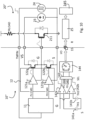
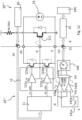
- the system comprises an electronic circuit is indicated with 10', as it includes the same components of circuit 10, i.e. the gate pre-driver 12, which is driven by the logic integrated circuit 11, and an Automated Testing Equipment 20'.
- the electronic circuit 10' in addition with respect to circuit 10 includes a time measuring unit 14, coupled between the gate terminal G and the source terminal S, which output is coupled through interface terminals 15 to an I/O interface 15 to a fast input output interface 25, for instance a fast SPI (Serial Peripheral Interface) interface in the automatic test equipment 20', which is shown in Figure 4 .
- the automatic test equipment 20' thus differs from the automatic test equipment 20 of figure 1 at least in that does not include the time measuring unit 14, which is instead comprised in the electronic circuit, in particular integrated circuit, 10'.
- the pre-driver 12 is coupled to the POWER FET/capacitive load 21 present on the automatic test equipment board 20' as well.
- the electronic circuit 10' includes the time measuring unit 14, coupled between the gate terminal G and the source terminal S, which output is coupled through the I/O interface terminals 15 to the interface 25.
- the time measuring unit 14 comprises a first comparator 142a, i.e. a differential amplifier, which positive input is coupled to the gate terminal G, while its negative input is coupled to the source terminal S, with interposed in series a first threshold generator voltage 141a, which applies a first threshold voltage TH1 to such negative input.
- the time measuring unit 14 further comprises a second comparator 142b, also a differential amplifier, which positive input is coupled to the gate terminal G, while its negative input is coupled to the source terminal S, with interposed in series a second threshold generator voltage 141b, which applies a second threshold voltage TH2 to such negative input.
- the output of the comparators 141a and 141b are brought to a multiplexer 143 which also receives the commands PU CMD and PD CMD, which in particular are counterphase signals, issued by the IC logic 11 to the pre-drivers 121a and 121b.
- the multiplexer 143 supplies the start signal SS and stop signal SP to a counter 144 under the control of a selection signal SEL also issued by the logic 11.
- the counter 144 supplies its output to a pass/fail check block 145, which in turn supplies its output to the input/output interface terminals 15.
- an automatic test equipment 20' corresponds to the automatic test equipment 20, however it does not include the time measuring unit 221.
- the automatic test equipment 20' includes instead an interface module 25 coupled to the input/output interface terminals 15 to receive the output of the pass/fail check block 145.
- the testing method may thus comprise the following steps:
- the system described with reference to figure 3 and perform thus may be configured to perform a built-in test sequence stored in the logic 11 to measure and check different parameters of the pre-driver 12.
- Such built-in self-test sequence of commands may comprise one or more test procedures, with reference to figures 5-9 and related description, including
- such built-in test sequence may include a Turn ON delay time test.
- a ON command signal of pre-driver for instance the command PU CMD low to high transition sent to the pull-up switch 122a, also sent to the multiplexer 143, is used to start (generating start signal SS) the internal counter 144.
- the multiplexer 143 under the control of the selection signal SEL issued by the logic 11 according to the built-in test sequence, selects the command PU CMD as start signal SS.
- the stop signal SP is then represented by the rising edge of comparator 142a, which output is also selected by the multiplexer 143, under the control of the selection signal SEL issued by the logic 11 according to the built-in test sequence.
- the time measured by the counter 144 is the turn ON time of the pre-driver 12. It is underlined that a comparator coupled to the gate and source terminals is normally present in the pre-driver architectures, named for instance VGS comparator, therefore, such already present comparator can be re-used as comparator 142a, without providing another comparator.
- such built-in test sequence may include a Turn OFF delay time test.
- the OFF command signal for instance the PD CMD low to high transition sent to the pull-down switch 122b, also sent to multiplexer 143, is used to start (generating start signal SS) an internal counter 144.
- the multiplexer 143 under the control of the selection signal SEL issued by the logic 11 according to the built-in test sequence, selects the rising edge of command PD CMD as start signal SS.
- the stop signal SP is the falling edge of comparator 141b, which output is also selected by the multiplexer 143, under the control of the selection signal SEL issued by the logic 11 according to the built-in test sequence.
- the time measured by the counter 144 is the turn OFF time of the predriver.
- a comparator which can be reused as comparator 141b is usually already present into pre-drivers architecture for instance to check the full VGS value.
- the counter 144 read-out is compared with a customizable pass-fail threshold, TH, in the pass/fail check block 145, if counter 144 value is below the threshold TH the check block 145 considers the test result good (pass) otherwise it is considered fail.
- TH a customizable pass-fail threshold
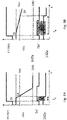
- FIG. 5A shows a behavior yielding a "pass" result R.
- the pullup command PU CMD is issued by logic 11, i.e. start signal SS for the counter 144, the gate source voltage VGS start rising after a delay and when it reaches the ON threshold TH1, the comparator 142a passes from low to high logic level, which is interpreted as stop signal SP for the counter 144.
- An elapsed time t e between the start and stop signal SS, SP is shown. The elapsed time t e is lower than the length of the threshold signal TH thus the result R of the test is pass.
- the threshold signal TH is shown here as a timeout duration, such as in watchdog counters, thus it may be the counter itself which has a timeout value, i.e. TH, stored, in particular set by the logic 11, and issues a timeout signal if the count of counter 144 surpasses the timeout value, which the pass/fail check logic 145 is configured to interpret as 'fail'.
- the counter 144 may simply send the ON duration measured, i.e. its count, to the pass/fail check logic 145, which compares them to the threshold TH, outputting a result R of pass or fail depending on the count being lower or greater than the threshold TH value indicated by the logic 11.
- Figure 5B in the same way shows a fail result.
- the slope of the gate source voltage VGS is less steep, resulting in a longer elapsed time before reaching ON threshold TH1, thus the elapsed time t e is longer than the threshold signal TH thus the result R of the test is fail for the ON time.
- a possible sequence executed by logic 11 as part of the built-in test for measuring turn OFF time is the following:
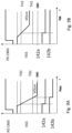
- FIG. 6A shows a pass result.
- the pulldown command PD CMD is issued by logic 11, i.e. start signal SS for the counter 144, the gate source voltage VGS start decreasing after a delay and when it reaches the OFF threshold TH2, the comparator 142b passes from high to low logic level, which is interpreted as stop signal SP for the counter.
- the elapsed time t e between the start and stop signal SS, SP is shown.
- the elapsed time t e is lower than the threshold signal TH' for OFF time internally configured thus the result R of the test is pass.
- Figure 6B in the same way shows a fail result.
- the slope of the gate source voltage VGS is less steep in its decrease, resulting in a longer elapsed time t e before reaching OFF threshold TH2, thus the elapsed time t e is longer than the threshold signal TH, thus the result R of the test is fail for the OFF time.
- the method according to embodiments may include that said built-in self-test sequence of commands comprises procedures for measuring an ON time or an OFF time respectively of the pre-driver 12 including
- the built-in test sequence may include operation performed by the system of figure 3 and 4 to perform also tests on the slew rate.
- an ON Slew rate test may include that a rising edge signal REa of comparator 142a, occurring at time t REa is used to start the internal counter 144, i.e. as start signal SS.
- the stop signal SP may be represented by a rising edge REb of comparator 142b occurring at time t REb .
- the time measured by the counter 144 allows the calculation of ON slew rate SR ON .
- the falling edge signal FEb of comparator 142b occurring at time t FEb is used to start, signal SS, the internal counter 144, while the stop signal SP is the falling edge FEa of comparator 142a occurring at time t FEa .
- the time measured by the counter 144 allows the calculation of OFF slew rate SR OFF .
- comparators 142a and comparators 142b may be already present in the pre-drivers architecture to check the gate source voltage.
- the solution may simply require to apply thresholds TH1, TH2 to such already present comparators, for instance by having controlled switches coupling the generators 141a, 141b to the respective negative input of comparators 142a, 142b during the built-in test sequence execution.
- a possible test executed by logic 11 as part of the built-in test for measuring ON slew rate may be the following:
- the built-in self-test sequence of commands may comprise a test procedure for measuring the ON slew rate and/or OFF slew rate respectively including
- the system of figures 3 and 4 can be used to perform also tests on the value of the Voltage Output Low logic level VOL and of the Voltage Output High logic level VOH.
- the comparator 142b can be configured with a threshold close (above) to the maximum value of the Voltage Output Low logic level VOL.
- the test is considered "pass” if the comparator 142b output state is 0. Otherwise, the test is fail.
- the comparator 142a can be configured with a threshold close (below) to the minimum value of Voltage Output High logic level VOH.
- the test is considered "pass” if the comparator output state is 1. Otherwise, the test is fail.
- a possible sequence for measuring Voltage Output High logic level VOH comprised in the built-in test sequence performed by logic 11 is the following:
- FIG 9A the gate source voltage VGS raises, after issuing PD CMD, toggling the first comparator 142a output then the second comparator 142b, i.e. passing thresholds TH1 and TH2, to reach a maximum Voltage Output Low logic level VOLm below the threshold TH1.
- gate source voltage VGS reaches a level above threshold TH1, therefore the output of second comparator 142b does not toggle.
- said built-in self-test sequence of commands may comprises a test procedure for measuring Voltage Output Low logic level VOL or Voltage Output High logic level VOH respectively, including
- the test on the ON/OFF Peak current makes use of the previously described method to test the slew rate, which in turns make use of thresholds TH1, TH2.
- peak current I peak can be retrieved by means of simple calculation by knowing the output capacitance C out on gate output terminal G.
- the test procedure for measuring the ON slew rate or OFF slew rate respectively comprises using a rising edge signal Rea of the first comparator 142a, occurring at a given time t REa as start signal SS, using a rising edge REb of the second comparator 142b occurring at a given time t REb as stop signal SP or using the falling edge signal FEb of the comparator 142b occurring at a given time t FEb as start signal (SS), while the stop signal SP is the falling edge FEa of comparator 142a occurring at a time t FEa , respectively.
- the test may include computing a ON slew rate SR ON or OFF slew rate SR OFF value respectively as ratio of the difference of the thresholds TH2, TH1 to the difference of time t REb - t REa , between the rising edges of comparators 142a and 142b or ratio of the difference of the thresholds TH2, TH1 to the difference t FEa - t FEb , of time between falling edges of comparators 142b, 142a, in particular computing an ON peak current or an OFF peak current as product of an output capacitance Cout and of said ON slew rate SR ON or OFF slew rate SR OFF .
- FIG 10 a second embodiment of the system for testing here described is shown.
- the electronic circuit 10 includes a counter 144 which however is coupled to the input/output interface 25 through terminals 15, without interposition of the pass/fail check 145 of figure 4 .
- the input/output interface 25 feeds the result of the counter 144 to a pass/fail check block 245 comprised in the automatic test equipment 20".
- the automatic test equipment 20" receives the counter 144 measured values and can configure test limits and compare it with such measured results to determine pass-fail criteria.
- FIG 11 a third embodiment of the system for testing here described is shown.
- the electronic circuit 10′′′ and automatic test equipment 20′′′ correspond to those of figure 10 , with the exception of an input/output test start interface 26 being present in the automatic test equipment 20", which is coupled to interface terminals 16 on the electronic circuit 10′′′, which bring signal to the logic 11.
- the automatic test equipment 20′′′ configures the test setup and test start with I/O communication interface 26.
- the information measured is sent to automatic test equipment through I/O interface 25.
- Automatic test equipment configures test limits and compares it with measured results to determine pass-fail criteria.
- the solution proposed reduces test time related cost by replacing all the test of a pre-drivers with built-in self-tests.
- the proposed solution has a negligible impact on design activity and requires only SPI communication interface because the test is done internally in the device.
- the proposed solution determines also cost saving at automatic test equipment level, since there is no need to connect and disconnect external instruments and no need to configure them.
- pre-drivers As inside a single integrated circuit there are several pre-drivers present, a plurality or all of such pre-drivers can be tested performing the built-in test sequence in parallel decreasing furthermore test time cost.
- this method could be useful for testing other architectures comprising pre-drivers and stages configured to supply a driving signal to a load, said stage comprising a pullup switch coupled to the voltage supply and a pulldown switch coupled to a lower potential than the voltage supply, in particular ground, coupled to each other in an output node, for instance, voltage buffers.
Landscapes
- Engineering & Computer Science (AREA)
- General Engineering & Computer Science (AREA)
- Physics & Mathematics (AREA)
- General Physics & Mathematics (AREA)
- Computer Hardware Design (AREA)
- Microelectronics & Electronic Packaging (AREA)
- Tests Of Electronic Circuits (AREA)
- Emergency Protection Circuit Devices (AREA)
Abstract
Description
- Embodiments of the present disclosure relate to techniques for testing electronic circuit, in particular integrated circuits, comprising pre-driver circuits.
- Embodiments of the present disclosure relate in particular to integrated circuits comprising drivers of active loads or capacitive loads and corresponding pre-driver circuits.
- Testing cost is one of the major contributions on the overall manufacturing cost of an electronic circuit, specifically of an integrated circuit.
- In integrated circuits are for instance used circuit configured to supply a current to a load, for instance, e.g. output drivers, by way of example in transmitting device. Such output drivers usually include a pair of switches, e.g. same type MOSFET transistor, arranged in series or totem pole between a voltage supply, to which the so-called pull-up switch is coupled, and a lower voltage such as ground, to which the so-called pull-down switch is coupled. The switches have a common node, usually the source of the pull-up switch coupled to the drain of the pull-down switch. A load can be represented by an active load or a capacitive load, and can be embodied by a circuit representing the load or a circuit component, e.g. capacitor.
- Also, they can be seen as half bridges, where the half bridge is made of two, e.g. N-channel, FET as switches, the low side coupled between ground and phase node, i.e. the common node, and the high side coupled between the battery voltage and phase node.
- In order to improve the behavior, for instance the dynamic characteristics, pre-driver circuits are provided which output is coupled to the control electrode, e.g. gate, of a respective switch to drive such switch with the current and/or dynamic required.
- Testing cost of gate pre-drivers depends on the number of parameters to be tested (high/low output voltage, current limitation/ peak current, rise/fall time. etc.) in order to guarantee the pre-driver functionality and detect possible defectiveness of manufacturing process. For each of these parameters a test is present at an automatic test equipment (ATE).
- In
figure 1 it is shown schematically a solution according to the prior art, where with thereference 10 is indicated anelectronic circuit 10, in particular an integrated electronic circuit, comprising a gate pre-driver 12, schematized as an operational amplifier-based circuit which is driven by a logicintegrated circuit 11. With 20 is indicated anAutomated Testing Equipment 20. Theelectronic circuit 10 comprises a voltage supply input terminal VS, which is coupled to the power supply terminal of the pre-driver 12. A gate output terminal G of theelectronic circuit 10 is, coupled to the output of the pre-driver 12, while a source terminal S is coupled to the other power supply terminal of the pre-driver 12. Also the integratedelectronic circuit 10 includes a test command input terminal TMPIN, which is coupled to an input of theintegrated circuit logic 11. - The
automatic test equipment 20, which is configure to couple through terminals G, S, TMPIN and to theelectronic circuit 10, comprises aload circuit 21, which is embodied by a power FET, but also can be embodied by a capacitive load, coupled by its two terminals between gate terminal G and source terminal S. In the case of a power FET, as shown infigure 2 , the gate terminal G is coupled to the gate of the power FET. Theautomatic test equipment 20 further comprises atime measurement unit 22 coupled between the same terminals G,S, avoltage power supply 23 coupled between the voltage supply terminal VS and ground GND, aPWM generator 24 coupled to the test command terminal TMPIN. - Thus, the pre-driver 12 is coupled to the
load circuit 21 in theautomatic test equipment 20, the voltage supply of the pre-driver 12 is supplied by thevoltage power supply 23 in theautomatic test equipment 20 and thelogic 11 receives test command signal SCMD from theexternal PWM generator 24 in the automatic test equipment through the test command terminal TMPIN. - Time measurements necessary to tests are performed with an automatic test equipment dedicated instrument, the
time measurement unit 22. - In
figure 1 is not shown the stage configured to supply a driving signal to a load, in particular a driver circuit, which is driven by the pre-driver 12, in order to better understand the coupling of the pre-driver 12 to theautomatic test equipment 21 for test. - In
figure 2 it is shown instead a more detailed view of an implementation of the circuits offigure 1 . TheIC logic 11 generates a pullup command PU CMD and a pull-down command PD CMD for each of a pre-driver 121a and 121b, comprised inpre-driver block 12 which are respectively coupled to the gates of apullup MOSFET 122a and a pull downMOSFET 122b, both N MOSFET in the example, which are the power output devices of adriver circuit 13, which represents a stage configured to supply a driving signal, e.g. current, to a load, and are coupled in a pull-up pull down configuration, i.e. the source ofpullup MOSFET 122a is coupled to the drain of thepulldown MOSFET 122b. The voltage supply at terminal VS is supplied to the voltage supply terminal ofdrivers up MOSFET 122a, while the source is coupled to the source terminal S. The central common node ofMOSFETS - In the
automatic test equipment 20 the gate terminal G is coupled to the gate of apower FET 211, representing theload circuit 21. The drain of thepower FET 211 is coupled to the voltage supply VCC by a load resistance Rload. The source of thepower FET 211 is coupled to the source terminal S and to the ground GND. Also an input of thetime measuring unit 22 is coupled to the gate terminal G, specifically is brought to an input of a comparator 222a and of a comparator 222b, which have programmable thresholds and provide start and stop signals SS, SP, to begin and to halt counting respectively, to acounter 221 comprised in theunit 22. As mentioned, a voltage generator embodies thevoltage power supply 23 and thePWM generator 24 supplies pulses to the command terminal TMPIN. - For instance the following steps of a testing procedure are performed, by the arrangement of
Figures 1 and2 : - the
automatic test equipment 20 couples all its modules 21-24 to the terminals TMPIN, VS, G, S of thecircuit 10; - a voltage supply VCC is fed by the
power supply 23, e.g. a voltage generator; thePWM generator 24 generates a command signal SCMD comprising a turn ON pulse on terminal TMPIN, i.e. for input to the logic integratedcircuit 11; - the
IC control logic 11 is configured on receiving such command signal SCMD comprising a turn ON pulse to de-activate the internal Pull down path, e.g. signal PD CMD is low so that the pre-driver 121b sends a logical low signal andswitch 122b is off, and activates internal pull up path e.g. signal PU CMD is high so that the pre-driver 121a send a logical high signal andswitch 122a is ON, in order to turn ON theexternal FET 211; - By such a solution all the parameters of a pre-driver are measured by coupling external instrumentation to pins, i.e. input and output terminals, of the pre-driver in order to read voltage, current or time interval. However, the coupling/decoupling of the automating test equipment is expensive in term of test time and could generate issue on test program repeatability.
- On the basis of the foregoing description, the need is felt for solutions which overcome one or more of the previously outlined drawbacks.
- According to one or more embodiments, such an object is achieved through a circuit having the features specifically set forth in the claims that follow. Embodiments moreover concerns a related system as well as a corresponding method.
- The claims are an integral part of the technical teaching of the disclosure provided herein.
- As mentioned in the foregoing, the present disclosure provides solutions regarding a system for testing comprising an electronic circuit to be tested and an automatic testing equipment,
- said electronic circuit to be tested comprising a stage configured to supply a driving signal to a load, said stage comprising a pullup switch coupled to the voltage supply and a pulldown switch coupled to a lower potential than the voltage supply, in particular ground, coupled to each other in an output node, and a pre-driver stage comprising pre-driver circuits which output is coupled to the control input of respective pullup and pull-down switch of the stage configured to supply a driving signal to a load,
- said electronic circuit to be tested comprising circuits for testing the pre-driver stage under the control of the automatic testing equipment comprising a test logic module configured to operate a built-in test sequence comprising test commands (PU CMD, PD CMD) for the pre-driver stage under the control of an external test signal issued by the automatic test equipment, the automatic test equipment comprising a load to be coupled to said output node of the stage configured to supply a driving signal to a load, said system for testing comprising a time measuring unit configured to measure duration of signals at the output of the driver stage coupled to a pass fail check module, configured to evaluate if said duration of signals at the output of the stage configured to supply a driving signal to a load satisfies a pass criterion,
- wherein
said time measuring unit is comprised in said electronic circuit to be tested and it started and stopped under the control of commands including commands issued by said logic during execution of said built-in test sequence. - In variant embodiments, said time measuring unit receives the signal at the output of the driver stage and compares such signal to at least one threshold.
- In variant embodiments, said electronic circuit to be tested comprises said pass fail check module.
- In variant embodiments, said electronic circuit to be tested comprises a series of output terminals for coupling the output of said time measuring unit with an input/output interface module in the automatic test equipment.
- In variant embodiments, said electronic circuit comprises a series of output terminal for coupling the output of said pass fail check module with an input/output interface module in the automatic test equipment.
- In variant embodiments, said automatic test equipment comprises a PWM module configured to send a command signal to said logic module through a command terminal of said electronic circuit to be tested to which the automatic test equipment is coupled.
- In variant embodiments, said automatic test equipment comprises an input/output interface module configured to send a command signal to said logic module through input interface terminals to which the automatic test equipment is coupled.
- In variant embodiments, said time measuring unit comprises a counter, configured to receive start and stop signal, respectively starting and stopping its count, a first and second comparator having one input coupled to the output node and the other input coupled to said lower potential node through a respective voltage generator generating a respective threshold voltage, a multiplexer receiving as input the outputs of said comparators, and the signals, in particular counterphase signals, at the output of said logic module issued to each of the pre-drivers and which two outputs are coupled so to represent the start and stop signals of said counter, said multiplexer being configured on the basis of a selection signal, in particular generated by the logic module, to select among its inputs said start and stop signals.
- In variant embodiments, said comparators correspond to comparators performing a voltage monitoring function, in particular VGS ON and VGS full on comparators, in the pre-driver circuit.
- The present disclosure also provides solutions regarding an electronic circuit to be tested configured to operate in the system of any of the embodiments.
- The present disclosure also provides solutions regarding a method for operating a system for testing according of any of the embodiments, comprising commanding by the automatic test equipment to the logic the execution of a built-in self-test sequence of commands,
said built-in self-test sequence of commands comprising issuing commands to operate, in particular activate or deactivate, the pre-driver stage according to a given mode of operation and commands to select signals operating said time measuring unit among said commands to operate the pre-driver stage and signals at the output of the stage configured to supply a driving signal to a load. - In variant embodiments, said built-in self-test sequence of commands comprises one or more test procedures including
- selecting among the commands to operate the pre-driver stage or the signals at the comparator outputs a start signal of the time measuring unit,
- selecting between the comparator outputs a stop signal of the time measuring unit,
- issuing a command to activate or deactivate the load,
- measuring a time duration by the time measuring unit between said start and stop signal,
- checking with respect to a respective threshold value if said time duration identifies a pass result or fail result of the test procedure.
- In variant embodiments, said built-in self-test sequence of commands comprises a procedure for measuring an ON time or an OFF time respectively of the pre-driver including
- selecting the activation commands or the deactivation command respectively of the pre-driver stage as start signal,
- selecting between the comparator outputs as stop signal of the time measuring unit the comparator having the lower threshold or the comparator having the higher threshold respectively,
- issuing a command to activate or respectively deactivate the load,
- measuring a time duration by the time measuring unit between said start and stop signal,
- checking with respect to a respective threshold value if said time duration identifies a pass result or fail result of the test procedure.
- In variant embodiments, said built-in self-test sequence of commands comprises a test procedure for measuring the ON slew rate or OFF slew rate including
- selecting between the signals at the output of the comparator having the lower threshold or at the output of the comparator having the higher threshold respectively a start signal of the time measuring unit,
- selecting between the signals at the output of the comparator having the higher threshold or at the output of the comparator having the lower threshold respectively a stop signal of the time measuring unit,
- issuing a command to activate or respectively deactivate the load,
- measuring a time duration by the time measuring unit between said start and stop signal,
- measuring a time duration by the time measuring unit between said start and stop signal,
- checking with respect to a respective threshold value if said time duration identifies a pass result or fail result of the test procedure.
- In variant embodiments, said built-in self-test sequence of commands comprises a test procedure for measuring Voltage Output Low logic level or Voltage Output High logic level respectively, including
- setting the lower threshold below a given Voltage Output Low logic level to be tested or the higher threshold above a given Voltage Output High logic level value to be tested respectively,
- issuing a command to activate or respectively deactivate the load,
- measuring a time duration by the time measuring unit between said start and stop signal,
- checking if the signals at the output of the comparator having the lower threshold or at the output of the comparator having the higher threshold both toggle or not.
- In variant embodiments, said test procedure for measuring the ON slew rate or OFF slew rate respectively comprises using a rising edge signal of the first comparator, occurring at a given time as start signal, using a rising edge of the second comparator occurring at a given time as stop signal or using the falling edge signal of the comparator occurring at a given time as start signal, while the stop signal is the falling edge of comparator occurring at a time, respectively.
- In variant embodiments, the method includes computing a ON slew rate or OFF slew rate value respectively as ratio of the difference of the thresholds to the difference of time between the rising edges of comparators or ratio of the difference of the thresholds to the difference of time between falling edges of comparators, in particular computing an ON peak current or an OFF peak current as product of an output capacitance and of said ON slew rate or OFF slew rate.
- The present disclosure also provides solutions regarding a computer program product that can be loaded into the memory of at least one computer and comprises parts of software code that are able to execute the steps of the method according to any of the previous embodiments when the product is run on at least one computer.
- Embodiments of the present disclosure will now be described with reference to the annexed drawings, which are provided purely by way of non-limiting example and in which:
-
Figure 1 and2 has already been described in the foregoing; -
Figure 3 shows schematically the circuit here described; -
Figure 4 shows an embodiment of the circuit offigure 3 ; -
Figures 5A, 5B show a time diagram of a first test performed by circuit ofFigure 3 in pass and fail conditions respectively; -
Figures 6A, 6B show a time diagram of a second test performed by circuit ofFigure 3 in pass and fail conditions respectively; -
Figures 7A, 7B show a time diagram of a third test performed by circuit ofFigure 3 in pass and fail conditions respectively; -
Figures 8A, 8B show a time diagram of a fourth test performed by circuit ofFigure 3 in pass and fail conditions respectively; -
Figures 9A, 9B show a time diagram of a fifth test performed by circuit ofFigure 3 in pass and fail conditions respectively; -
Figure 10 shows a second embodiment of the circuit offigure 3 ; -
Figure 11 shows a third embodiment of the circuit offigure 3 . - In the following description, numerous specific details are given to provide a thorough understanding of embodiments. The embodiments can be practiced without one or several specific details, or with other methods, components, materials, etc. In other instances, well-known structures, materials, or operations are not shown or described in detail to avoid obscuring aspects of the embodiments.
- Reference throughout this specification to "one embodiment" or "an embodiment" means that a particular feature, structure, or characteristic described in connection with the embodiment is included in at least one embodiment. Thus, the appearances of the phrases "in one embodiment" or "in an embodiment" in various places throughout this specification are not necessarily all referring to the same embodiment. Furthermore, the particular features, structures, or characteristics may be combined in any suitable manner in one or more embodiments.
- The headings provided herein are for convenience only and do not interpret the scope or meaning of the embodiments.
- Figures parts, elements or components which have already been described with reference to
Figure 1 and2 are denoted by the same references previously used in such Figures; the description of such previously described elements will not be repeated in the following in order not to overburden the present detailed description. - The main parameters to be tested for pre-drivers includes delay times, slew rates, output low voltage VOL, output high voltage VOH and ON/OFF peak current. The solution here described provides capability to measure all such parameters by a unique built-in self-test, embedded into the integrated circuit, based on an internal time measuring unit comprising internal configurable voltage monitors and internal counter.
- This allows to measure all relevant test parameters inside the integrated circuit and then compare them with expected value, preferably also inside the integrated circuit. The final result of the comparation (Pass/Fail) is sent to the automatic test equipment through a fast communication interface.
- In
figure 3 it is shown the solution here described of system for testing following the general schematization ofFigure 1 . Below a simplified scheme of the proposed solution is reported. Same numbers indicate components with a same function. - The system comprises an electronic circuit is indicated with 10', as it includes the same components of
circuit 10, i.e. thegate pre-driver 12, which is driven by the logic integratedcircuit 11, and an Automated Testing Equipment 20'. The electronic circuit 10' in addition with respect tocircuit 10 includes atime measuring unit 14, coupled between the gate terminal G and the source terminal S, which output is coupled throughinterface terminals 15 to an I/O interface 15 to a fastinput output interface 25, for instance a fast SPI (Serial Peripheral Interface) interface in the automatic test equipment 20', which is shown inFigure 4 . The automatic test equipment 20' thus differs from theautomatic test equipment 20 offigure 1 at least in that does not include thetime measuring unit 14, which is instead comprised in the electronic circuit, in particular integrated circuit, 10'. - The pre-driver 12 is coupled to the POWER FET/
capacitive load 21 present on the automatic test equipment board 20' as well. - Thus, in general the electronic circuit 10' and the
automatic test equipment 20 are operated as follows: - firstly, the supply voltage VCC is provided to the pre-driver 12 by the automatic test equipment 20' through the
voltage supply generator 23 coupled to terminal VS and a signal SCMD with a ON pulse on the terminal TMPIN is used to start a built-in self-test executed bylogic 11 upon receiving signal SCMD; - secondly, the pre-driver 12 is turned ON/OFF and time measurements are all performed by the circuit 10' using the
time measuring unit 14; - finally, the duration values measured by the
time measuring unit 14, or the consequent results of the pass/fail check performed on the same circuit 10', are passed to automatic test equipment 20' through thefast communication interface 25. - In
figure 4 it is shown instead a more detailed view of an implementation of the circuits offigure 3 . Also in this case, with respect to the implementation of prior art circuits offigure 2 , same numbers indicate components with a same function. As mentioned, the electronic circuit 10' includes thetime measuring unit 14, coupled between the gate terminal G and the source terminal S, which output is coupled through the I/O interface terminals 15 to theinterface 25. - The
time measuring unit 14 comprises afirst comparator 142a, i.e. a differential amplifier, which positive input is coupled to the gate terminal G, while its negative input is coupled to the source terminal S, with interposed in series a firstthreshold generator voltage 141a, which applies a first threshold voltage TH1 to such negative input. Thetime measuring unit 14 further comprises asecond comparator 142b, also a differential amplifier, which positive input is coupled to the gate terminal G, while its negative input is coupled to the source terminal S, with interposed in series a secondthreshold generator voltage 141b, which applies a second threshold voltage TH2 to such negative input. The output of thecomparators multiplexer 143 which also receives the commands PU CMD and PD CMD, which in particular are counterphase signals, issued by theIC logic 11 to the pre-drivers 121a and 121b. Themultiplexer 143 supplies the start signal SS and stop signal SP to acounter 144 under the control of a selection signal SEL also issued by thelogic 11. Thecounter 144 supplies its output to a pass/fail check block 145, which in turn supplies its output to the input/output interface terminals 15. As shown, an automatic test equipment 20' corresponds to theautomatic test equipment 20, however it does not include thetime measuring unit 221. The automatic test equipment 20' includes instead aninterface module 25 coupled to the input/output interface terminals 15 to receive the output of the pass/fail check block 145. - The testing method may thus comprise the following steps:
- the automatic test equipment 20' is coupled to the terminals of the electronic circuit 10', TMPIN, VS, G, S, and to the
interface terminals 15; - the voltage supply VCC is fed through the pin VS by the
supply voltage generator 23; - the
PWM generator 24 generates a pulse with a rising edge on the pin TMPIN as command SCMD; - the pre-driver testmode logic, i.e.,
logic 11, starts a built-in self-test sequence of commands in which an internal microcontroller comprised in thelogic 11, but not shown in the figures, manages a test sequence of operations in order to measure parameters of the pre-driver 12; - the test sequence provides measurements of pre-driver 12 parameters based on the output of the
counter 144 controlled by the configurable start and stop signals SS, SP, which in the example offigure 4 are represented by signals at the output of the comparators and signals relevant for pre-driver control, i.e. commands PU CMD and PD CMD; - the values measured by the
counter 144 are compared with internal configurable threshold, e.g. TH, TH', TH", TH‴ as shown inFigures 5 ,6 ,7 ,8 and pass-fail check is performed inblock 145; - the result of pass/fail check in
block 145 is sent to automatic test equipment 20' equipment through I/O interface 15. - The system described with reference to
figure 3 and perform thus may be configured to perform a built-in test sequence stored in thelogic 11 to measure and check different parameters of the pre-driver 12. - This corresponds in general to performing a method for operating a system for testing such as the one of
figure 3 or4 comprising commanding SCMD by the automatic test equipment 20' to thelogic 11 the execution of a built-in self-test sequence of commands,
said built-in self-test sequence of commands comprising issuing commands PU CMD, PD CMD to operate, in particular activate or deactivate, thepre-driver stage 12 according to a given mode of operation and commands SEL to select signals SS, SP operating saidtime measuring unit 14 among said commands PU CMD, PD CMD to operate thepre-driver stage 12 and signals at the output G of thedriver stage - Such built-in self-test sequence of commands may comprise one or more test procedures, with reference to
figures 5-9 and related description, including - selecting SEL among the commands PU CMD, PD CMD to operate the
pre-driver stage 12 or the signals at thecomparator time measuring unit 14, - selecting between the
comparator outputs - issuing a command PU CMD, PD CMD to activate or deactivate the load, e.g. FET, 211,
- measuring a time duration te by the
time measuring unit 14 between said start SS and stop signal SP,
checking 145 with respect to a respective threshold value TH, TH', TH", TH‴ - if said time duration te identifies a pass result or fail result of the test procedure.
- For instance, such built-in test sequence may include a Turn ON delay time test. In such test a ON command signal of pre-driver, for instance the command PU CMD low to high transition sent to the pull-
up switch 122a, also sent to themultiplexer 143, is used to start (generating start signal SS) theinternal counter 144. In other words, themultiplexer 143, under the control of the selection signal SEL issued by thelogic 11 according to the built-in test sequence, selects the command PU CMD as start signal SS. The stop signal SP is then represented by the rising edge ofcomparator 142a, which output is also selected by themultiplexer 143, under the control of the selection signal SEL issued by thelogic 11 according to the built-in test sequence. The time measured by thecounter 144 is the turn ON time of the pre-driver 12. It is underlined that a comparator coupled to the gate and source terminals is normally present in the pre-driver architectures, named for instance VGS comparator, therefore, such already present comparator can be re-used ascomparator 142a, without providing another comparator. - For instance, such built-in test sequence may include a Turn OFF delay time test. In such test the OFF command signal, for instance the PD CMD low to high transition sent to the pull-
down switch 122b, also sent to multiplexer 143, is used to start (generating start signal SS) aninternal counter 144. In other words, themultiplexer 143, under the control of the selection signal SEL issued by thelogic 11 according to the built-in test sequence, selects the rising edge of command PD CMD as start signal SS. The stop signal SP is the falling edge ofcomparator 141b, which output is also selected by themultiplexer 143, under the control of the selection signal SEL issued by thelogic 11 according to the built-in test sequence. The time measured by thecounter 144 is the turn OFF time of the predriver. Also a comparator which can be reused ascomparator 141b is usually already present into pre-drivers architecture for instance to check the full VGS value. - The
counter 144 read-out is compared with a customizable pass-fail threshold, TH, in the pass/fail check block 145, ifcounter 144 value is below the threshold TH thecheck block 145 considers the test result good (pass) otherwise it is considered fail. - Thus, a possible test executed by
logic 11 as part of the built-in test for measuring turn ON time is the following: - the thresholds TH1 of
comparator 141a is configured; - pass-fail criteria are configured, e.g. the value of pass-fail threshold TH;
- counter 144 is reset and ready to start;
- start and stop signals SS, SP used in the test are selected by the
multiplexer 143 selector signal SEL, selecting the pullup command PU CMD as start signal SS, and the output of thecomparator 141a as stop signal SP. The pullup command PU_CMD is sent to both pre-driver 141a andmultiplexer 143 providing the start signal SS for thecounter 144. The stop signal SP is provided by thecomparator 141a when its output goes to high level as the voltage on its inputs, gate source voltage VGS between gate G and source S terminals, exceeds ON threshold TH1; - the
external FET 211 is turned ON, in particular by asserting the command PU CMD to high, i.e. asserting the start signal SS; - counter 144 measures ON time;
- block 145 compares measured ON time with the internally configured pass fail threshold TH, in particular in the pass/
fail block 145; - block 145 sends to the
interface 25 of the automatic test equipment 20' through the terminals 15 a pass-fail result R, e.g. assuming pass (good, measured ON time lower than threshold TH) or fail (bad, measured ON time greater than chosen threshold TH) values. - The corresponding signals are shown in
figure 5A , which shows a behavior yielding a "pass" result R. As the pullup command PU CMD is issued bylogic 11, i.e. start signal SS for thecounter 144, the gate source voltage VGS start rising after a delay and when it reaches the ON threshold TH1, thecomparator 142a passes from low to high logic level, which is interpreted as stop signal SP for thecounter 144. An elapsed time te between the start and stop signal SS, SP is shown. The elapsed time te is lower than the length of the threshold signal TH thus the result R of the test is pass. - The threshold signal TH is shown here as a timeout duration, such as in watchdog counters, thus it may be the counter itself which has a timeout value, i.e. TH, stored, in particular set by the
logic 11, and issues a timeout signal if the count ofcounter 144 surpasses the timeout value, which the pass/fail check logic 145 is configured to interpret as 'fail'. In other embodiments, thecounter 144 may simply send the ON duration measured, i.e. its count, to the pass/fail check logic 145, which compares them to the threshold TH, outputting a result R of pass or fail depending on the count being lower or greater than the threshold TH value indicated by thelogic 11. -
Figure 5B in the same way shows a fail result. The slope of the gate source voltage VGS is less steep, resulting in a longer elapsed time before reaching ON threshold TH1, thus the elapsed time te is longer than the threshold signal TH thus the result R of the test is fail for the ON time. - A possible sequence executed by
logic 11 as part of the built-in test for measuring turn OFF time is the following: - pass-fail criteria are configured, e.g. the value of a pass fail threshold TH', which may be different with respect to threshold TH for the ON test, or not;
- counter 144 is reset and ready to start;
- start and stop signals SS, SP are selected by the
multiplexer 143 selector signal SEL, selecting the pulldown command PD CMD as start signal SS, and the output of thecomparator 142b as stop signal SP. The pulldown command PD CMD is sent to both pre-driver 142a andmultiplexer 143 providing the start signal SS for thecounter 144. The stop signal SP is provided by thecomparator 142b when its output goes to low level as the voltage on its inputs, gate source voltage VGS between gate G and source S terminals, exceeds OFF threshold TH2 (also called "full ON" threshold); -
external FET 211 is turned OFF, in particular by asserting the command PD CMD to low, i.e. asserting the start signal SS; - thus, counter 144 measure OFF time;
- block 145 compares measured OFF time with the internally configured pass fail threshold TH';
- block 145 sends to the
interface 25 of the automatic test equipment 20' through theterminals 15 pass-fail result R. - The corresponding signals are shown in
figure 6A , which shows a pass result. As the pulldown command PD CMD is issued bylogic 11, i.e. start signal SS for thecounter 144, the gate source voltage VGS start decreasing after a delay and when it reaches the OFF threshold TH2, thecomparator 142b passes from high to low logic level, which is interpreted as stop signal SP for the counter. The elapsed time te between the start and stop signal SS, SP is shown. The elapsed time te is lower than the threshold signal TH' for OFF time internally configured thus the result R of the test is pass. -
Figure 6B in the same way shows a fail result. The slope of the gate source voltage VGS is less steep in its decrease, resulting in a longer elapsed time te before reaching OFF threshold TH2, thus the elapsed time te is longer than the threshold signal TH, thus the result R of the test is fail for the OFF time. - Summing up, the method according to embodiments may include that said built-in self-test sequence of commands comprises procedures for measuring an ON time or an OFF time respectively of the pre-driver 12 including
- selecting SEL the activation commands PU CMD or the deactivation command PD CMD respectively of the
pre-driver stage 12 as start signal, - selecting between the
comparator outputs first comparator 142a having the lower threshold TH1 or thesecond comparator 142b having the higher threshold TH2 respectively, - issuing a command PU CMD, PD CMD to activate or respectively deactivate the
load 211, - measuring a time duration te by the
time measuring unit 14 between said start SS and stop signal SP, - checking 145 with respect to a respective threshold value TH, TH' if said time duration te identifies a pass result or fail result of the test procedure.
- The built-in test sequence may include operation performed by the system of
figure 3 and4 to perform also tests on the slew rate. - For instance, an ON Slew rate test may include that a rising edge signal REa of
comparator 142a, occurring at time tREa is used to start theinternal counter 144, i.e. as start signal SS. The stop signal SP may be represented by a rising edge REb ofcomparator 142b occurring at time tREb. The time measured by thecounter 144 allows the calculation of ON slew rate SRON. - Dually, for an OFF Slew rate test, the falling edge signal FEb of
comparator 142b occurring at time tFEb is used to start, signal SS, theinternal counter 144, while the stop signal SP is the falling edge FEa ofcomparator 142a occurring at time tFEa. The time measured by thecounter 144 allows the calculation of OFF slew rate SROFF. - Thus, it is:

- As mentioned, according to an important aspect of the solution here described,
comparators 142a andcomparators 142b may be already present in the pre-drivers architecture to check the gate source voltage. Thus the solution may simply require to apply thresholds TH1, TH2 to such already present comparators, for instance by having controlled switches coupling thegenerators comparators - Thus, a possible test executed by
logic 11 as part of the built-in test for measuring ON slew rate may be the following: - the thresholds TH1 and TH2 of
comparators - pass-fail criteria are configured, e.g. the value of a pass-fail threshold TH". Start and stop signals SS, SP are selected by
multiplexer 143 selector signal SEL, selecting the outputs ofcomparators comparator 142a, occurring at time tREa is used to start theinternal counter 144, i.e. as start signal SS. The stop signal SP may be represented by a rising edge Reb ofcomparator 142b occurring at time tREb ; - the
counter 144 is reset and ready to start; - the
external FET 211 is turned ON, by the pullup command signal PU CMD; - the
counter 144 measures time between rising edges ofcomparators comparators - the
block 145 compares measured time between rising edges ofcomparators - block 145 sends to the
interface 25 of the automatic test equipment 20' through theterminals 15 pass-fail result R. If slew rate measured by thecounter 144 is lower than the configured threshold TH", than the ON slew rate value is considered to pass the test. Otherwise on slew rate value is considered to fail the test. - This exemplified in time diagram of
figure 7A (pass) andfigure 7B (fail). - In the same way, a possible test executed by
logic 11 as part of the built-in test for measuring OFF slew rate is the following: - the threshold TH1 and TH2 of
comparators - pass-fail criteria are configured, e.g. the value of a pass-fail threshold TH‴. Start and stop signals SS, SP are selected by
mux 143 selector signal SEL, selecting the outputs ofcomparators Comparators counter 144. The falling edge signal FEb ofcomparator 142b occurring at time tFEb is used to start theinternal counter 144, while the stop signal SP is the falling edge FEa ofcomparator 142a occurring at time tFEa ; - counter 144 is reset and ready to start;
-
external FET 211 is turned OFF, by the pull-down command PD CMD; - the
counter 144 measures time between falling edges ofcomparators comparators - block 145 compares measured time between falling edges of
comparators - block 145 sends to the
interface 25 of the automatic test equipment 20' through theterminals 15 pass-fail result R. If the slew rate measured by thecounter 144 is lower than the configured threshold TH‴, than the OFF slew rate value is considered to pass the test. Otherwise OFF slew rate value is considered to fail the test. - This exemplified in time diagram of
figure 8A (pass) andfigure 8B (fail). - Thus, the built-in self-test sequence of commands may comprise a test procedure for measuring the ON slew rate and/or OFF slew rate respectively including
- selecting between the signals at the output of the first comparator having the lower threshold TH1 or at the output of the
second comparator 142b having the higher threshold TH2 respectively a start signal SS of thetime measuring unit 14, - selecting SEL between the signals at the output of the
second comparator 142b having the higher threshold TH2 or at the output of thefirst comparator 142a having the lower threshold TH1 respectively a stop signal SP of the time measuring unit, - issuing a command PU CMD, PD CMD to activate or respectively deactivate the
load 211, - measuring a time duration by the time measuring unit between said start and stop signal,
- measuring a time duration te by the
time measuring unit 14 between said start SS and stop signal SP, - checking 145 with respect to a respective threshold value TH", TH‴ if said time duration te identifies a pass result or fail result of the test procedure.
- The system of
figures 3 and4 can be used to perform also tests on the value of the Voltage Output Low logic level VOL and of the Voltage Output High logic level VOH. - For instance, to measure Voltage Output Low logic level VOL, the
comparator 142b can be configured with a threshold close (above) to the maximum value of the Voltage Output Low logic level VOL. When the pre-driver 121a is in OFF state, the test is considered "pass" if thecomparator 142b output state is 0. Otherwise, the test is fail. - Dually, to measure the Voltage Output High logic level VOH, the
comparator 142a can be configured with a threshold close (below) to the minimum value of Voltage Output High logic level VOH. When the pre-driver 121a is in ON state, the test is considered "pass" if the comparator output state is 1. Otherwise, the test is fail. - A possible sequence for measuring Voltage Output High logic level VOH comprised in the built-in test sequence performed by
logic 11 is the following: - if comparator thresholds TH1 and TH2 are crossed by the gate source voltage VGS, then both
comparators - otherwise test is considered fail.
- This exemplified in time diagram of
figure 9A (pass) andfigure 9B (fail), which represent testing Voltage Output Low logic level VOL. Infigure 9A the gate source voltage VGS raises, after issuing PD CMD, toggling thefirst comparator 142a output then thesecond comparator 142b, i.e. passing thresholds TH1 and TH2, to reach a maximum Voltage Output Low logic level VOLm below the threshold TH1. Infigure 9B gate source voltage VGS reaches a level above threshold TH1, therefore the output ofsecond comparator 142b does not toggle. Dually, testing of a Voltage Output High logic level VOH is possible, after issuing PU CMD, by checking the toggling output of the comparators whether a minimum Voltage Output High logic level VOH, above TH2, is reached. This second test is not shown in the figures. - Thus, said built-in self-test sequence of commands may comprises a test procedure for measuring Voltage Output Low logic level VOL or Voltage Output High logic level VOH respectively, including
- setting the lower threshold TH1 above a given maximum Voltage Output Low logic level VOL to be tested or the higher threshold TH2 below a given minimum Voltage Output High logic level VOH value to be tested respectively,
- issuing a command PU CMD, PD CMD to activate or respectively deactivate the
load 211, - checking 145 if the signals at the output of the
comparator 142a having the lower threshold TH1 or at the output of thecomparator 142b having the higher threshold TH2 both toggle or not. - The system of
figures 3 and4 can be used to perform also tests on the ON/OFF Peak current. This test may be just a calculation based on the previously described slew rate tests, giving values SRON and SROFF. Knowing, the output capacitance Cout associated to load 21, the value of thresholds TH1, TH2 and the measure of theinternal counter 144, the ON/OFF peak current can be measured by the following equations:

- Basically, the test on the ON/OFF Peak current makes use of the previously described method to test the slew rate, which in turns make use of thresholds TH1, TH2. Once SRON and SROFF values are measured with the already described method, peak current Ipeak can be retrieved by means of simple calculation by knowing the output capacitance Cout on gate output terminal G.
- Thus, the test procedure for measuring the ON slew rate or OFF slew rate respectively comprises using a rising edge signal Rea of the
first comparator 142a, occurring at a given time tREa as start signal SS, using a rising edge REb of thesecond comparator 142b occurring at a given time tREb as stop signal SP or using the falling edge signal FEb of thecomparator 142b occurring at a given time tFEb as start signal (SS), while the stop signal SP is the falling edge FEa ofcomparator 142a occurring at a time tFEa , respectively. - Then, the test may include computing a ON slew rate SRON or OFF slew rate SROFF value respectively as ratio of the difference of the thresholds TH2, TH1 to the difference of time tREb - tREa , between the rising edges of
comparators comparators - In
figure 10 a second embodiment of the system for testing here described is shown. In this case theelectronic circuit 10" includes acounter 144 which however is coupled to the input/output interface 25 throughterminals 15, without interposition of the pass/fail check 145 offigure 4 . The input/output interface 25 feeds the result of thecounter 144 to a pass/fail check block 245 comprised in theautomatic test equipment 20". In this case, after the execution of the built-in test at thecircuit 10", theautomatic test equipment 20" receives thecounter 144 measured values and can configure test limits and compare it with such measured results to determine pass-fail criteria. - In
figure 11 a third embodiment of the system for testing here described is shown. In this case, theelectronic circuit 10‴ andautomatic test equipment 20‴ correspond to those offigure 10 , with the exception of an input/outputtest start interface 26 being present in theautomatic test equipment 20", which is coupled tointerface terminals 16 on theelectronic circuit 10‴, which bring signal to thelogic 11. In this case theautomatic test equipment 20‴ configures the test setup and test start with I/O communication interface 26. At the end of test the information measured is sent to automatic test equipment through I/O interface 25. Automatic test equipment configures test limits and compares it with measured results to determine pass-fail criteria. - The described solution thus has several advantages with respect to the prior art solutions.
- The solution proposed reduces test time related cost by replacing all the test of a pre-drivers with built-in self-tests.
- Also, the proposed solution has a negligible impact on design activity and requires only SPI communication interface because the test is done internally in the device.
- The proposed solution determines also cost saving at automatic test equipment level, since there is no need to connect and disconnect external instruments and no need to configure them.
- Of course, without prejudice to the principle of the invention, the details of construction and the embodiments may vary widely with respect to what has been described and illustrated herein purely by way of example, without thereby departing from the scope of the present invention, as defined by the ensuing claims.
- As inside a single integrated circuit there are several pre-drivers present, a plurality or all of such pre-drivers can be tested performing the built-in test sequence in parallel decreasing furthermore test time cost.
- Moreover this method could be useful for testing other architectures comprising pre-drivers and stages configured to supply a driving signal to a load, said stage comprising a pullup switch coupled to the voltage supply and a pulldown switch coupled to a lower potential than the voltage supply, in particular ground, coupled to each other in an output node, for instance, voltage buffers.
Claims (18)
- A system for testing comprising an electronic circuit to be tested and an automatic testing equipment,said electronic circuit (10; 10'; 10"; 10‴) to be tested comprising a stage (122a, 122b) configured to supply a driving signal to a load, said stage (122a, 122b) comprising a pullup switch (122a) coupled to the voltage supply (VS) and a pulldown switch coupled to a lower potential than the voltage supply (GND, S), in particular ground, coupled to each other in an output node (G), and a pre-driver stage (12) comprising pre-driver circuits (121a, 121b) which output is coupled to the control input of respective pullup (122a) and pull down (122b) switch of the stage (122a, 122b) configured to supply a driving signal to a load,said electronic circuit (10; 10';1 0"; 10‴) to be tested comprising circuits (11, 14) for testing the pre-driver stage (12) under the control (SCMD) of the automatic testing equipment (20; 20'; 20"; 20‴) comprising a test logic module (11) configured to operate a built-in test sequence comprising test commands (PU CMD, PD CMD) for the pre-driver stage under the control of an external test signal (SCMD) issued by the automatic test equipment, the automatic test equipment (20, 20', 20") comprising a test load (211) to be coupled to said output node (G) of the stage (122a, 122b) configured to supply a driving signal to a load, said system for testing comprising a time measuring unit (14) configured to measure duration of signals at the output (G) of the stage (122a, 122b) configured to supply a driving signal to a load coupled to a pass fail check module (145), configured to evaluate if said duration of signals at the output (G) of the stage (122a, 122b) configured to supply a driving signal to a load satisfies a pass criterion,wherein
said time measuring unit (14) is comprised in said electronic circuit to be tested and it started and stopped under the control of commands including commands ((PU CMD, PD CMD, SEL) issued by said logic (11) during execution of said bult-in test sequence. - System according to claim 1, wherein said time measuring unit (14) receives the signal (VGS) at the output of the stage (122a, 122b) configured to supply a driving signal to a load and compares such signal to at least one threshold (TH1, TH2).
- System according to claim 1, wherein said electronic circuit (10') to be tested comprises said pass fail check module (145).
- System according to claim 1, wherein said electronic circuit (10'; 10"; 10‴) to be tested comprises a series of output terminals (15) for coupling the output of said time measuring unit (14) with an input/output interface module (25) in the automatic test equipment (20'; 20"; 20‴).
- System according to claim 3, wherein said electronic circuit comprise a series of output terminal (15) for coupling the output of said pass fail check module (145) with an input/output interface module (25) in the automatic test equipment (20').
- System according to claim 1, wherein said automatic test equipment (20'; 20") comprise a PWM module configured to send a command signal to said logic module (11) through a command terminal (TMPIN) of said electronic circuit to be tested (10'; 10") to which the automatic test equipment (20'; 20") is coupled.
- System according to claim 1, wherein said automatic test equipment (20‴) comprise an input/output interface module (26) configured to send a command signal to said logic module (11) through input interface terminals (16) to which the automatic test equipment (20‴) is coupled.
- System according to any of the previous claims wherein said time measuring unit (14) comprises a counter (144), configured to receive start and stop signal (SS, SP), respectively starting and stopping its count, a first (142a) and second (142b) comparator having one input coupled to the output node (G) and the other input coupled to said lower potential node (S) through a respective voltage generator (141a, 141b) generating a respective threshold voltage (TH1, TH2), a multiplexer (144) receiving as input the outputs of said comparators (142a, 142b), and the signals (PU_CMD, PD_CMD), in particular counterphase signals, at the output of said logic module (11) issued to each of the pre-drivers (121a, 121b) and which two outputs are coupled so to represent the start (SS) and stop (SP) signals of said counter (144), said multiplexer (143) being configured on the basis of a selection signal (SEL), in particular generated by the logic module (11), to select among its inputs said start (SS) and stop (SP) signals.
- System according to claim 8, wherein said comparators (142a, 142b) correspond to comparators performing a voltage monitoring function, in particular VGS ON and VGS full on comparators, in the pre-driver circuit.
- An electronic circuit to be tested configured to operate in the system of any of claims 1 to 9.
- A method for operating a system for testing according to any of claims 1 to 10, comprising commanding (SCMD) by the automatic test equipment (20') to the logic (11) the execution of a built-in self-test sequence of commands,
said built-in self-test sequence of commands comprising issuing commands (PU CMD, PD CMD) to operate, in particular activate or deactivate, the pre-driver stage (12) according to a given mode of operation and commands (SEL) to select signals (SS, SP) operating said time measuring unit (14) among said commands (PU CMD, PD CMD) to operate the pre-driver stage (12) and signals at the output (G) of the stage (122a, 122b) configured to supply a driving signal to a load. - A method according to claim 11, wherein said built-in self-test sequence of commands comprises one or more test procedures includingselecting (SEL) among the commands (PU CMD, PD CMD) to operate the pre-driver stage (12) or the signals at the comparator (142a, 142b) outputs a start signal (SS) of the time measuring unit (14),selecting between the comparator outputs (142a, 142b) a stop signal (SP) of the time measuring unit,issuing a command (PU CMD, PD CMD) to activate or deactivate the load (211),measuring a time duration (te) by the time measuring unit (14) between said start (SS) and stop signal (SP),checking (145) with respect to a respective threshold value (TH, TH', TH", TH‴) if said time duration (te) identifies a pass result or fail result of the test procedure.
- A method according to claim 12, wherein said built-in self-test sequence of commands comprises a procedure for measuring an ON time or an OFF time respectively of the pre-driver (12) includingselecting (SEL) the activation commands (PU CMD) or the deactivation command (PD CMD) respectively of the pre-driver stage (12) as start signal,selecting between the comparator outputs (142a, 142b) as stop signal (SP) of the time measuring unit the comparator (142a) having the lower threshold (TH1) or the comparator (142a) having the higher threshold (TH2) respectively,issuing a command (PU CMD, PD CMD) to activate or respectively deactivate the load (211),measuring a time duration (te) by the time measuring unit (14) between said start (SS) and stop signal (SP),checking (145) with respect to a respective threshold value (TH, TH') if said time duration (te) identifies a pass result or fail result of the test procedure.
- A method according to claim 12, wherein said built-in self-test sequence of commands comprises a test procedure for measuring the ON slew rate or OFF slew rate includingselecting (SEL) between the signals at the output of the comparator (142a) having the lower threshold (TH1) or at the output of the comparator (142b) having the higher threshold (TH2) respectively a start signal (SS) of the time measuring unit (14),selecting (SEL) between the signals at the output of the comparator (142b) having the higher threshold (TH2) or at the output of the comparator (142a) having the lower threshold (TH1) respectively a stop signal (SP) of the time measuring unit,issuing a command (PU CMD, PD CMD) to activate or respectively deactivate the load (211),measuring a time duration by the time measuring unit between said start and stop signal,measuring a time duration (te) by the time measuring unit (14) between said start (SS) and stop signal (SP),checking (145) with respect to a respective threshold value (TH", TH‴) if said time duration (te) identifies a pass result or fail result of the test procedure.
- A method according to claim 11, wherein said built-in self-test sequence of commands comprises a test procedure for measuring Voltage Output Low logic level (VOL) or Voltage Output High logic level (VOH) respectively, includingsetting the lower threshold (TH1) above a given Voltage Output Low logic level (VOL) to be tested or the higher threshold (TH2) below a given Voltage Output High logic level (VOH) value to be tested respectively,issuing a command (PU CMD, PD CMD) to activate or respectively deactivate the load (211),measuring a time duration (te) by the time measuring unit (14) between said start (SS) and stop signal (SP),checking (145) if the signals at the output of the comparator (142a) having the lower threshold (TH1) or at the output of the comparator (142b) having the higher threshold (TH2) both toggle or not.
- A method according to claim 12, wherein said test procedure for measuring the ON slew rate or OFF slew rate respectively comprises using a rising edge signal (Rea) of the first comparator (142a), occurring at a given time ( tREa ) as start signal (SS), using a rising edge (Reb) of the second comparator (142b) occurring at a given time (tREb ) as stop signal (SP) or using the falling edge signal (FEb) of the comparator 142b occurring at a given time (tFEb ) as start signal (SS), while the stop signal (SP) is the falling edge (FEa) of comparator 142a occurring at a time ( tFEa ), respectively.
- A method according to claim 16, including computing a ON slew rate (SRON) or OFF slew rate (SROFF) value respectively as ratio of the difference of the thresholds (TH2, TH1) to the difference of time ( tREb - tREa ,) between the rising edges of comparators (142a and 142b) or ratio of the difference of the thresholds (TH2, TH1) to the difference (tFEa - tFEb , ) of time between falling edges of comparators (142b, 142a), in particular computing an ON peak current or an OFF peak current as product of an output capacitance (Cout) and of said ON slew rate (SRON) or OFF slew rate (SROFF).
- A computer program product that can be loaded into the memory of at least one computer and comprises parts of software code that are able to execute the steps of the method of any of Claims 11 to 15 when the product is run on at least one computer.
Applications Claiming Priority (1)
| Application Number | Priority Date | Filing Date | Title |
|---|---|---|---|
| IT102021000023438A IT202100023438A1 (en) | 2021-09-10 | 2021-09-10 | TEST SYSTEM OF AN ELECTRONIC CIRCUIT AND CORRESPONDING PROCEDURE AND COMPUTER PRODUCT |
Publications (2)
| Publication Number | Publication Date |
|---|---|
| EP4148436A1 true EP4148436A1 (en) | 2023-03-15 |
| EP4148436B1 EP4148436B1 (en) | 2025-06-25 |
Family
ID=78649956
Family Applications (1)
| Application Number | Title | Priority Date | Filing Date |
|---|---|---|---|
| EP22192346.9A Active EP4148436B1 (en) | 2021-09-10 | 2022-08-26 | A system for testing an electronic circuit and corresponding method and computer program product |
Country Status (4)
| Country | Link |
|---|---|
| US (1) | US12072372B2 (en) |
| EP (1) | EP4148436B1 (en) |
| CN (1) | CN116068367A (en) |
| IT (1) | IT202100023438A1 (en) |
Citations (4)
| Publication number | Priority date | Publication date | Assignee | Title |
|---|---|---|---|---|
| US20050108606A1 (en) * | 2003-11-17 | 2005-05-19 | Georg Muller | Input/output switching arrangement for semiconductor circuits, a method for testing driver circuits in semiconductor circuits |
| US20080077835A1 (en) * | 2006-09-27 | 2008-03-27 | Khoche A Jay | Automatic Test Equipment Receiving Diagnostic Information from Devices with Built-in Self Test |
| US20080195920A1 (en) * | 2007-02-13 | 2008-08-14 | Freescale Semiconductor, Inc. | Self-test structure and method of testing a digital interface |
| US20200256914A1 (en) * | 2019-02-07 | 2020-08-13 | Nuvoton Technology Corporation | Slew Rate Programming in Automatic Test Equipment (ATE) |
Family Cites Families (5)
| Publication number | Priority date | Publication date | Assignee | Title |
|---|---|---|---|---|
| US5822228A (en) * | 1997-05-27 | 1998-10-13 | Lsi Logic Corporation | Method for using built in self test to characterize input-to-output delay time of embedded cores and other integrated circuits |
| US10126353B2 (en) * | 2015-03-23 | 2018-11-13 | Infineon Technologies Ag | Verification of gate driver protection logic |
| ITUA20163454A1 (en) * | 2016-05-16 | 2017-11-16 | St Microelectronics Srl | ERROR DETECTION CIRCUIT FOR A PWM PILOT CIRCUIT, ITS RELATED SYSTEM AND INTEGRATED CIRCUIT |
| US11070218B2 (en) * | 2019-04-17 | 2021-07-20 | Texas Instruments Incorporated | Real time counter-based method for the determination and measurement of frequency lock time in phase-locked loops |
| US11552633B1 (en) * | 2021-10-15 | 2023-01-10 | Stmicroelectronics S.R.L. | Driver circuit with enhanced control for current and voltage slew rates |
-
2021
- 2021-09-10 IT IT102021000023438A patent/IT202100023438A1/en unknown
-
2022
- 2022-08-26 EP EP22192346.9A patent/EP4148436B1/en active Active
- 2022-09-06 US US17/903,344 patent/US12072372B2/en active Active
- 2022-09-09 CN CN202211103398.2A patent/CN116068367A/en active Pending
Patent Citations (4)
| Publication number | Priority date | Publication date | Assignee | Title |
|---|---|---|---|---|
| US20050108606A1 (en) * | 2003-11-17 | 2005-05-19 | Georg Muller | Input/output switching arrangement for semiconductor circuits, a method for testing driver circuits in semiconductor circuits |
| US20080077835A1 (en) * | 2006-09-27 | 2008-03-27 | Khoche A Jay | Automatic Test Equipment Receiving Diagnostic Information from Devices with Built-in Self Test |
| US20080195920A1 (en) * | 2007-02-13 | 2008-08-14 | Freescale Semiconductor, Inc. | Self-test structure and method of testing a digital interface |
| US20200256914A1 (en) * | 2019-02-07 | 2020-08-13 | Nuvoton Technology Corporation | Slew Rate Programming in Automatic Test Equipment (ATE) |
Also Published As
| Publication number | Publication date |
|---|---|
| EP4148436B1 (en) | 2025-06-25 |
| US12072372B2 (en) | 2024-08-27 |
| US20230079831A1 (en) | 2023-03-16 |
| CN116068367A (en) | 2023-05-05 |
| IT202100023438A1 (en) | 2023-03-10 |
Similar Documents
| Publication | Publication Date | Title |
|---|---|---|
| US6836136B2 (en) | Pin driver for AC and DC semiconductor device testing | |
| US6215324B1 (en) | Dynamic burn-in test equipment | |
| KR19990082339A (en) | Assemblies and Methods for Testing Integrated Circuit Devices | |
| CN115113014B (en) | Power device turn-off failure characteristic testing device and testing method | |
| US20140327450A1 (en) | Device and method for testing the state of the connection of a load connected to a connection point | |
| CN101034127A (en) | Verifying individual probe contact using shared tester channels | |
| CN108181570B (en) | Chip grounding pin connectivity test method and device and readable storage medium | |
| CN202548256U (en) | Short-circuit test device | |
| JP2654352B2 (en) | Semiconductor integrated circuit | |
| US6262585B1 (en) | Apparatus for I/O leakage self-test in an integrated circuit | |
| EP4148436B1 (en) | A system for testing an electronic circuit and corresponding method and computer program product | |
| US12445038B2 (en) | Turn on delay measurements for capacitive load | |
| US8618812B2 (en) | Electrical interconnection integrated device with fault detecting module and electronic apparatus comprising the device | |
| US6918073B2 (en) | Differential self-test of input/output circuits | |
| US5642364A (en) | Contactless testing of inputs and outputs of integrated circuits | |
| US5343479A (en) | Semiconductor integrated circuit having therein circuit for detecting abnormality of logical levels outputted from input buffers | |
| EP0436358B1 (en) | Integrated circuit having power supply connection integrity monitor | |
| US11131711B1 (en) | Testing system and method for in chip decoupling capacitor circuits | |
| US5826004A (en) | Input/output device with self-test capability in an integrated circuit | |
| CN120949142A (en) | Multi-range calibration for single-pin parameter measurement units | |
| US20050030056A1 (en) | Apparatus for measuring VS parameters in a wafer burn-in system | |
| JP2020128977A (en) | Device and method for automatically testing electronic device | |
| US7772875B2 (en) | Input/output circuit for evaluating delay | |
| US12596159B2 (en) | Multi-wire bonding test circuit for a converter | |
| KR102918304B1 (en) | Test circuit monitoring pbti and operating method of thereof |
Legal Events
| Date | Code | Title | Description |
|---|---|---|---|
| PUAI | Public reference made under article 153(3) epc to a published international application that has entered the european phase |
Free format text: ORIGINAL CODE: 0009012 |
|
| STAA | Information on the status of an ep patent application or granted ep patent |
Free format text: STATUS: THE APPLICATION HAS BEEN PUBLISHED |
|
| AK | Designated contracting states |
Kind code of ref document: A1 Designated state(s): AL AT BE BG CH CY CZ DE DK EE ES FI FR GB GR HR HU IE IS IT LI LT LU LV MC MK MT NL NO PL PT RO RS SE SI SK SM TR |
|
| STAA | Information on the status of an ep patent application or granted ep patent |
Free format text: STATUS: REQUEST FOR EXAMINATION WAS MADE |
|
| 17P | Request for examination filed |
Effective date: 20230914 |
|
| RBV | Designated contracting states (corrected) |
Designated state(s): AL AT BE BG CH CY CZ DE DK EE ES FI FR GB GR HR HU IE IS IT LI LT LU LV MC MK MT NL NO PL PT RO RS SE SI SK SM TR |
|
| GRAP | Despatch of communication of intention to grant a patent |
Free format text: ORIGINAL CODE: EPIDOSNIGR1 |
|
| STAA | Information on the status of an ep patent application or granted ep patent |
Free format text: STATUS: GRANT OF PATENT IS INTENDED |
|
| INTG | Intention to grant announced |
Effective date: 20250220 |
|
| GRAS | Grant fee paid |
Free format text: ORIGINAL CODE: EPIDOSNIGR3 |
|
| GRAA | (expected) grant |
Free format text: ORIGINAL CODE: 0009210 |
|
| STAA | Information on the status of an ep patent application or granted ep patent |
Free format text: STATUS: THE PATENT HAS BEEN GRANTED |
|
| AK | Designated contracting states |
Kind code of ref document: B1 Designated state(s): AL AT BE BG CH CY CZ DE DK EE ES FI FR GB GR HR HU IE IS IT LI LT LU LV MC MK MT NL NO PL PT RO RS SE SI SK SM TR |
|
| REG | Reference to a national code |
Ref country code: GB Ref legal event code: FG4D |
|
| REG | Reference to a national code |
Ref country code: CH Ref legal event code: EP |
|
| REG | Reference to a national code |
Ref country code: CH Ref legal event code: EP |
|
| REG | Reference to a national code |
Ref country code: IE Ref legal event code: FG4D |
|
| REG | Reference to a national code |
Ref country code: DE Ref legal event code: R096 Ref document number: 602022016347 Country of ref document: DE |
|
| PG25 | Lapsed in a contracting state [announced via postgrant information from national office to epo] |
Ref country code: FI Free format text: LAPSE BECAUSE OF FAILURE TO SUBMIT A TRANSLATION OF THE DESCRIPTION OR TO PAY THE FEE WITHIN THE PRESCRIBED TIME-LIMIT Effective date: 20250625 |
|
| REG | Reference to a national code |
Ref country code: LT Ref legal event code: MG9D |
|
| PG25 | Lapsed in a contracting state [announced via postgrant information from national office to epo] |
Ref country code: NO Free format text: LAPSE BECAUSE OF FAILURE TO SUBMIT A TRANSLATION OF THE DESCRIPTION OR TO PAY THE FEE WITHIN THE PRESCRIBED TIME-LIMIT Effective date: 20250925 Ref country code: GR Free format text: LAPSE BECAUSE OF FAILURE TO SUBMIT A TRANSLATION OF THE DESCRIPTION OR TO PAY THE FEE WITHIN THE PRESCRIBED TIME-LIMIT Effective date: 20250926 |
|
| PG25 | Lapsed in a contracting state [announced via postgrant information from national office to epo] |
Ref country code: BG Free format text: LAPSE BECAUSE OF FAILURE TO SUBMIT A TRANSLATION OF THE DESCRIPTION OR TO PAY THE FEE WITHIN THE PRESCRIBED TIME-LIMIT Effective date: 20250625 |
|
| PG25 | Lapsed in a contracting state [announced via postgrant information from national office to epo] |
Ref country code: HR Free format text: LAPSE BECAUSE OF FAILURE TO SUBMIT A TRANSLATION OF THE DESCRIPTION OR TO PAY THE FEE WITHIN THE PRESCRIBED TIME-LIMIT Effective date: 20250625 |
|
| PGFP | Annual fee paid to national office [announced via postgrant information from national office to epo] |
Ref country code: AT Payment date: 20251020 Year of fee payment: 4 |
|
| PG25 | Lapsed in a contracting state [announced via postgrant information from national office to epo] |
Ref country code: RS Free format text: LAPSE BECAUSE OF FAILURE TO SUBMIT A TRANSLATION OF THE DESCRIPTION OR TO PAY THE FEE WITHIN THE PRESCRIBED TIME-LIMIT Effective date: 20250925 |
|
| PG25 | Lapsed in a contracting state [announced via postgrant information from national office to epo] |
Ref country code: LV Free format text: LAPSE BECAUSE OF FAILURE TO SUBMIT A TRANSLATION OF THE DESCRIPTION OR TO PAY THE FEE WITHIN THE PRESCRIBED TIME-LIMIT Effective date: 20250625 |
|
| REG | Reference to a national code |
Ref country code: NL Ref legal event code: MP Effective date: 20250625 |
|
| PG25 | Lapsed in a contracting state [announced via postgrant information from national office to epo] |
Ref country code: NL Free format text: LAPSE BECAUSE OF FAILURE TO SUBMIT A TRANSLATION OF THE DESCRIPTION OR TO PAY THE FEE WITHIN THE PRESCRIBED TIME-LIMIT Effective date: 20250625 |
|
| PG25 | Lapsed in a contracting state [announced via postgrant information from national office to epo] |
Ref country code: PT Free format text: LAPSE BECAUSE OF FAILURE TO SUBMIT A TRANSLATION OF THE DESCRIPTION OR TO PAY THE FEE WITHIN THE PRESCRIBED TIME-LIMIT Effective date: 20251027 |
|
| REG | Reference to a national code |
Ref country code: AT Ref legal event code: MK05 Ref document number: 1806978 Country of ref document: AT Kind code of ref document: T Effective date: 20250625 |
|
| PG25 | Lapsed in a contracting state [announced via postgrant information from national office to epo] |
Ref country code: IS Free format text: LAPSE BECAUSE OF FAILURE TO SUBMIT A TRANSLATION OF THE DESCRIPTION OR TO PAY THE FEE WITHIN THE PRESCRIBED TIME-LIMIT Effective date: 20251025 |
|
| PG25 | Lapsed in a contracting state [announced via postgrant information from national office to epo] |
Ref country code: AT Free format text: LAPSE BECAUSE OF FAILURE TO SUBMIT A TRANSLATION OF THE DESCRIPTION OR TO PAY THE FEE WITHIN THE PRESCRIBED TIME-LIMIT Effective date: 20250625 Ref country code: SM Free format text: LAPSE BECAUSE OF FAILURE TO SUBMIT A TRANSLATION OF THE DESCRIPTION OR TO PAY THE FEE WITHIN THE PRESCRIBED TIME-LIMIT Effective date: 20250625 |
|
| PG25 | Lapsed in a contracting state [announced via postgrant information from national office to epo] |
Ref country code: CZ Free format text: LAPSE BECAUSE OF FAILURE TO SUBMIT A TRANSLATION OF THE DESCRIPTION OR TO PAY THE FEE WITHIN THE PRESCRIBED TIME-LIMIT Effective date: 20250625 |
|
| PG25 | Lapsed in a contracting state [announced via postgrant information from national office to epo] |
Ref country code: PL Free format text: LAPSE BECAUSE OF FAILURE TO SUBMIT A TRANSLATION OF THE DESCRIPTION OR TO PAY THE FEE WITHIN THE PRESCRIBED TIME-LIMIT Effective date: 20250625 |
|
| PG25 | Lapsed in a contracting state [announced via postgrant information from national office to epo] |
Ref country code: EE Free format text: LAPSE BECAUSE OF FAILURE TO SUBMIT A TRANSLATION OF THE DESCRIPTION OR TO PAY THE FEE WITHIN THE PRESCRIBED TIME-LIMIT Effective date: 20250625 |
|
| PG25 | Lapsed in a contracting state [announced via postgrant information from national office to epo] |
Ref country code: SK Free format text: LAPSE BECAUSE OF FAILURE TO SUBMIT A TRANSLATION OF THE DESCRIPTION OR TO PAY THE FEE WITHIN THE PRESCRIBED TIME-LIMIT Effective date: 20250625 |
|
| PG25 | Lapsed in a contracting state [announced via postgrant information from national office to epo] |
Ref country code: ES Free format text: LAPSE BECAUSE OF FAILURE TO SUBMIT A TRANSLATION OF THE DESCRIPTION OR TO PAY THE FEE WITHIN THE PRESCRIBED TIME-LIMIT Effective date: 20250625 |
|
| REG | Reference to a national code |
Ref country code: DE Ref legal event code: R119 Ref document number: 602022016347 Country of ref document: DE |
|
| PG25 | Lapsed in a contracting state [announced via postgrant information from national office to epo] |
Ref country code: RO Free format text: LAPSE BECAUSE OF FAILURE TO SUBMIT A TRANSLATION OF THE DESCRIPTION OR TO PAY THE FEE WITHIN THE PRESCRIBED TIME-LIMIT Effective date: 20250625 |
|
| REG | Reference to a national code |
Ref country code: CH Ref legal event code: H13 Free format text: ST27 STATUS EVENT CODE: U-0-0-H10-H13 (AS PROVIDED BY THE NATIONAL OFFICE) Effective date: 20260324 |
|
| PG25 | Lapsed in a contracting state [announced via postgrant information from national office to epo] |
Ref country code: MC Free format text: LAPSE BECAUSE OF FAILURE TO SUBMIT A TRANSLATION OF THE DESCRIPTION OR TO PAY THE FEE WITHIN THE PRESCRIBED TIME-LIMIT Effective date: 20250625 |
|
| PG25 | Lapsed in a contracting state [announced via postgrant information from national office to epo] |
Ref country code: DK Free format text: LAPSE BECAUSE OF FAILURE TO SUBMIT A TRANSLATION OF THE DESCRIPTION OR TO PAY THE FEE WITHIN THE PRESCRIBED TIME-LIMIT Effective date: 20250625 |
|
| PG25 | Lapsed in a contracting state [announced via postgrant information from national office to epo] |
Ref country code: LU Free format text: LAPSE BECAUSE OF NON-PAYMENT OF DUE FEES Effective date: 20250826 Ref country code: IT Free format text: LAPSE BECAUSE OF FAILURE TO SUBMIT A TRANSLATION OF THE DESCRIPTION OR TO PAY THE FEE WITHIN THE PRESCRIBED TIME-LIMIT Effective date: 20250625 |
|
| PG25 | Lapsed in a contracting state [announced via postgrant information from national office to epo] |
Ref country code: CH Free format text: LAPSE BECAUSE OF NON-PAYMENT OF DUE FEES Effective date: 20250831 |
|
| PLBE | No opposition filed within time limit |
Free format text: ORIGINAL CODE: 0009261 |
|
| STAA | Information on the status of an ep patent application or granted ep patent |
Free format text: STATUS: NO OPPOSITION FILED WITHIN TIME LIMIT |
|
| REG | Reference to a national code |
Ref country code: CH Ref legal event code: L10 Free format text: ST27 STATUS EVENT CODE: U-0-0-L10-L00 (AS PROVIDED BY THE NATIONAL OFFICE) Effective date: 20260507 |