EP4147281B1 - Ein verfahren zur herstellung einer hochtemperatur-supraleiter-feldspule und einehochtemperatur-supraleiter-feldspule - Google Patents
Ein verfahren zur herstellung einer hochtemperatur-supraleiter-feldspule und einehochtemperatur-supraleiter-feldspule Download PDFInfo
- Publication number
- EP4147281B1 EP4147281B1 EP21723965.6A EP21723965A EP4147281B1 EP 4147281 B1 EP4147281 B1 EP 4147281B1 EP 21723965 A EP21723965 A EP 21723965A EP 4147281 B1 EP4147281 B1 EP 4147281B1
- Authority
- EP
- European Patent Office
- Prior art keywords
- hts
- coil
- tapes
- field coil
- coils
- Prior art date
- Legal status (The legal status is an assumption and is not a legal conclusion. Google has not performed a legal analysis and makes no representation as to the accuracy of the status listed.)
- Active
Links
Images




Classifications
-
- G—PHYSICS
- G21—NUCLEAR PHYSICS; NUCLEAR ENGINEERING
- G21B—FUSION REACTORS
- G21B1/00—Thermonuclear fusion reactors
- G21B1/11—Details
-
- H—ELECTRICITY
- H01—ELECTRIC ELEMENTS
- H01F—MAGNETS; INDUCTANCES; TRANSFORMERS; SELECTION OF MATERIALS FOR THEIR MAGNETIC PROPERTIES
- H01F41/00—Apparatus or processes specially adapted for manufacturing or assembling magnets, inductances or transformers; Apparatus or processes specially adapted for manufacturing materials characterised by their magnetic properties
- H01F41/02—Apparatus or processes specially adapted for manufacturing or assembling magnets, inductances or transformers; Apparatus or processes specially adapted for manufacturing materials characterised by their magnetic properties for manufacturing cores, coils, or magnets
- H01F41/04—Apparatus or processes specially adapted for manufacturing or assembling magnets, inductances or transformers; Apparatus or processes specially adapted for manufacturing materials characterised by their magnetic properties for manufacturing cores, coils, or magnets for manufacturing coils
- H01F41/048—Superconductive coils
-
- H—ELECTRICITY
- H01—ELECTRIC ELEMENTS
- H01F—MAGNETS; INDUCTANCES; TRANSFORMERS; SELECTION OF MATERIALS FOR THEIR MAGNETIC PROPERTIES
- H01F6/00—Superconducting magnets; Superconducting coils
- H01F6/06—Coils, e.g. winding, insulating, terminating or casing arrangements therefor
-
- G—PHYSICS
- G21—NUCLEAR PHYSICS; NUCLEAR ENGINEERING
- G21B—FUSION REACTORS
- G21B1/00—Thermonuclear fusion reactors
- G21B1/05—Thermonuclear fusion reactors with magnetic or electric plasma confinement
- G21B1/057—Tokamaks
-
- Y—GENERAL TAGGING OF NEW TECHNOLOGICAL DEVELOPMENTS; GENERAL TAGGING OF CROSS-SECTIONAL TECHNOLOGIES SPANNING OVER SEVERAL SECTIONS OF THE IPC; TECHNICAL SUBJECTS COVERED BY FORMER USPC CROSS-REFERENCE ART COLLECTIONS [XRACs] AND DIGESTS
- Y02—TECHNOLOGIES OR APPLICATIONS FOR MITIGATION OR ADAPTATION AGAINST CLIMATE CHANGE
- Y02E—REDUCTION OF GREENHOUSE GAS [GHG] EMISSIONS, RELATED TO ENERGY GENERATION, TRANSMISSION OR DISTRIBUTION
- Y02E30/00—Energy generation of nuclear origin
- Y02E30/10—Nuclear fusion reactors
-
- Y—GENERAL TAGGING OF NEW TECHNOLOGICAL DEVELOPMENTS; GENERAL TAGGING OF CROSS-SECTIONAL TECHNOLOGIES SPANNING OVER SEVERAL SECTIONS OF THE IPC; TECHNICAL SUBJECTS COVERED BY FORMER USPC CROSS-REFERENCE ART COLLECTIONS [XRACs] AND DIGESTS
- Y10—TECHNICAL SUBJECTS COVERED BY FORMER USPC
- Y10S—TECHNICAL SUBJECTS COVERED BY FORMER USPC CROSS-REFERENCE ART COLLECTIONS [XRACs] AND DIGESTS
- Y10S505/00—Superconductor technology: apparatus, material, process
- Y10S505/825—Apparatus per se, device per se, or process of making or operating same
- Y10S505/848—Radiant energy application
-
- Y—GENERAL TAGGING OF NEW TECHNOLOGICAL DEVELOPMENTS; GENERAL TAGGING OF CROSS-SECTIONAL TECHNOLOGIES SPANNING OVER SEVERAL SECTIONS OF THE IPC; TECHNICAL SUBJECTS COVERED BY FORMER USPC CROSS-REFERENCE ART COLLECTIONS [XRACs] AND DIGESTS
- Y10—TECHNICAL SUBJECTS COVERED BY FORMER USPC
- Y10S—TECHNICAL SUBJECTS COVERED BY FORMER USPC CROSS-REFERENCE ART COLLECTIONS [XRACs] AND DIGESTS
- Y10S505/00—Superconductor technology: apparatus, material, process
- Y10S505/825—Apparatus per se, device per se, or process of making or operating same
- Y10S505/88—Inductor
Definitions
- the present invention relates to a method of manufacturing High Temperature Superconductor (HTS) field coils and to HTS field coils.
- HTS High Temperature Superconductor
- High temperature superconductors HTS
- low temperature superconductors LTS materials
- All low temperature superconductors have a critical temperature (the temperature above which the material cannot be superconducting even in zero magnetic field) below about 30K.
- the behaviour of HTS material is not described by BCS theory, and such materials may have critical temperatures above about 30 K (though it should be noted that it is the physical differences in composition and superconducting operation, rather than the critical temperature, which define HTS and LTS material).
- HTS cuprate superconductors
- cuprate superconductors ceramics based on cuprates (compounds containing a copper oxide group), such as BSCCO, or ReBCO (where Re is a rare earth element, commonly Y or Gd).
- BSCCO cuprate superconductors
- ReBCO where Re is a rare earth element, commonly Y or Gd.
- Other HTS materials include iron pnictides (e.g. FeAs and FeSe) and magnesium diboride (MgB 2 ).
- ReBCO is typically manufactured as tapes, with a structure as shown in Figure 1 .
- Such tape 100 is generally approximately 100 microns thick, and includes a substrate 101 (typically electropolished nickel-molybdenum alloy such as Hastelloy TM , approximately 50 microns thick), on which is deposited by Ion Beam Assisted Deposition (IBAD), magnetron sputtering, or another suitable technique a series of buffer layers known as the buffer stack 102, of approximate thickness 0.2 microns.
- IBAD Ion Beam Assisted Deposition
- An epitaxial ReBCO-HTS layer 103 overlays the buffer stack, and is typically 1 micrometer thick.
- MOCVD Metal Oxide Chemical Vapour Deposition
- a 1-2 micrometer silver layer 104 is deposited on the HTS layer by sputtering or another suitable technique, and a copper stabilizer layer 105 is deposited on the tape by electroplating or another suitable technique.
- the silver layer 104 and copper stabilizer layer 105 are deposited on the sides of the tape 100 and the substrate 101 too, so that these layers extend continuously around the perimeter of the tape 100, thereby allowing an electrical connection to be made to the ReBCO-HTS layer 103 from either face of the tape 100.
- These layers 104, 105 may therefore also be referred to as "cladding".
- the silver cladding has a uniform thickness on both the sides and edges of the tape of around 1-2 microns.
- Providing a silver layer 104 between the HTS layer 103 and the copper layer 105 prevents the HTS material contacting the copper, which might lead to the HTS material becoming poisoned by the copper.
- the parts of the silver layer 104 and copper stabilizer layer 105 on the sides of the tape 100 are not shown in Figure 1 for clarity, but are shown in the cross section view provided in Figure 9 .
- Figure 1 also does not show the silver layer 104 extending beneath the substrate 101, as is normally the case (see Figure 9 , for example).
- the silver layer 104 makes a low resistivity electrical interface to, and an hermetic protective seal around, the ReBCO layer 103, whilst the copper layer 105 enables external connections to be made to the tape (e.g. permits soldering) and provides a parallel conductive path for electrical stabilisation.
- the substrate 101 provides a mechanical backbone that can be fed through the manufacturing line and permit growth of subsequent layers.
- the buffer stack 102 provides a biaxially textured crystalline template upon which to grow the HTS layer, and prevents chemical diffusion of elements from the substrate to the HTS which damage its superconducting properties.
- the silver layer 104 provides a low resistance interface from the ReBCO-HTS layer 103 to the stabiliser layer 105, and the stabiliser layer 105 provides an alternative current path in the event that any part of the ReBCO ceases superconducting (enters the "normal" state).
- exfoliated HTS tape can be manufactured, which lacks a substrate (e.g. Hastelloy TM substrate) and buffer stack, but typically has a "surround coating" of silver, i.e. layers on both sides and the edges of the HTS layer. Tape which has a substrate will be referred to as "substrated" HTS tape.
- HTS tapes may be arranged into HTS cables.
- An HTS cable comprises one or more HTS tapes, which are connected along their length via conductive material (normally copper).
- the HTS tapes may be stacked (i.e. arranged such that the HTS layers are parallel), or they may have some other arrangement of tapes, which may vary along the length of the cable.
- Notable special cases of HTS cables are single HTS tapes, and HTS pairs.
- HTS pairs comprise a pair of HTS tapes, arranged such that the HTS layers are parallel. Where substrated tape is used, HTS pairs may be type-0 (with the HTS layers facing each other), type-1 (with the HTS layer of one tape facing the substrate of the other), or type-2 (with the substrates facing each other).
- HTS cables comprising more than two tapes may arrange some or all of the tapes in HTS pairs.
- Stacked HTS tapes may comprise various arrangements of HTS pairs, most commonly either a stack of type-1 pairs or a stack of type-0 pairs and (or, equivalently, type-2 pairs).
- HTS cables may comprise a mix of substrated and exfoliated tape.
- Wound coils are manufactured by wrapping an HTS cable 201 (shown as a solid line) around a former 202 in a continuous spiral.
- the former is shaped to provide the required inner perimeter of the coil, and may be a structural part of the final wound coil, or may be removed after winding.
- Sectional coils as shown schematically in Figure 3 , are composed of several sections 301, each of which may contain several cables or preformed busbars 311 (shown as solid lines) and will form an arc of the overall coil.
- the sections are connected by joints 302 to form the complete coil. While the turns of the coils in Figures 2 and 3 are shown spaced apart for clarity, there will generally be material connecting the turns of the coil - e.g. they may be consolidated by potting with epoxy.
- the coils may be "insulated” - having electrical insulating material between the turns of the coil (e.g. so that there is a turn-to-turn resistance of around 1 Ohm or greater), or "non-insulated", where the turns of the coil are electrically connected radially (i.e. connected by an electrical conductor material), as well as along the cables (e.g. by connecting the copper stabiliser layers of the cables by soldering or by direct contact).
- Insulated HTS coils can be used in applications in which large, rapid changes in magnetic field are required, such as plasma control in fusion magnets.
- non-insulated coils are generally not suitable for large field coils, due to extremely high ramp-up times.
- a middle ground option is a "partially insulated" coil, where the material between turns has resistance intermediate between that of a traditional electrical conductor, e.g. a metal, and a that of a traditional electrical insulator, such as ceramic or organic insulator, e.g. having a resistivity between 100 and 10 16 times that of copper or between 10 -6 and 10 8 Ohm metre.
- a traditional electrical conductor e.g. a metal
- a traditional electrical insulator such as ceramic or organic insulator, e.g. having a resistivity between 100 and 10 16 times that of copper or between 10 -6 and 10 8 Ohm metre.
- Partially insulated HTS magnets i.e. HTS magnets with a partially conductive turn-to-turn connection (i.e. a turn-to-turn connection with material of an "intermediate" resistivity between 10 -6 and 10 8 Ohm-metre)
- the turn-to-turn resistivity value may be too low to be implemented on large (high inductance) coils.
- the electromagnetic time constant associated with a coil is determined by the ratio of the coil's inductance to its resistance (L/R)
- high inductance coils require correspondingly "high" turn-to-turn resistances so that the coil can respond to changing electrical current/magnetic field on a suitable timescale.
- the geometry of the turn-to-turn connection, or its limited thermal connection to the magnet can result in excessive Ohmic-heating during discharge, leading to electrical burnout of the connection. This may occur, for example, when a partially insulated magnet is formed by introducing a PCB between the turns: the thin metal tracks of the PCB are generally thermally insulated from the rest of the magnet by the polyimide insulation.
- FIG 4 shows a radial cross section of a specific type of wound coil known as a "pancake coil", in which HTS cables (tapes) 401 are wrapped to form a flat coil, in a similar manner to a spool of ribbon.
- Pancake coils may be made with an inner perimeter which is any two dimensional shape.
- pancake coils are provided as a "double pancake coil”, as shown in the radial cross section of Figure 5 , which comprises two pancake coils 501, 502 wound in an opposite sense to one another, with insulation 503 between the pancake coils, and with the inner terminals connected together 504.
- This configuration means that voltage only needs to be supplied to the outer terminals 521, 522 (which are generally more accessible) to drive current through the turns of the coil and thereby generate a magnetic field.
- the situation can be improved by contracting the donut-shaped torus of a conventional tokamak to its limit, having the appearance of a cored apple - the 'spherical' tokamak (ST).
- START tokamak at Culham demonstrated a huge increase in efficiency - the magnetic field required to contain a hot plasma can be reduced by a factor of 10.
- plasma stability is improved, and build costs may be reduced.
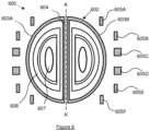
- the magnet coils in a tokamak can be divided into two groups.
- the poloidal field coils are horizontal circular coils wound with their centre located on the central column of the tokamak, and produce a poloidal field (i.e. a magnetic field which is substantially parallel to the central column).
- the toroidal field coils are wound vertically through the central column, and around the outside of the plasma chamber (the "return limbs") to produce a toroidal field (i.e. a magnetic field which is circular around the central column).
- the combination of the poloidal and toroidal fields produces a helical magnetic field within the plasma chamber that keeps the plasma confined.
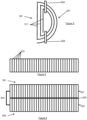
- Figure 7 shows a cross section of the central column 604, which comprises a plurality of current carrying assemblies 701, through which the central column sections of the TF coils pass.
- Space in the central column 604 is taken up by both the current carrying assemblies and non-current carrying components, including, for example:
- Figure 8 shows one of the sectors 701 of the central column 604.
- the sector 701 comprising three current carrying assemblies 801A-C which make up the TF coil 602.
- Each assembly comprises one or more HTS field coils 801, e.g. a pancake coil or double pancake coil. It is apparent from Figure 8 that the rectangular cross sections of the HTS field coils do not fit well into the arc-shaped cross section of the sector 701 and a large amount of space is wasted that more than could be usefully used for other components, such as additional cooling channels or sensors.
- the arrangement of the current carrying assemblies 801A-C within the sector 701 also results in high stresses at the corners of the cross section of the HTS coils (as discussed below in relation to Figure 19 ).
- US2002/144838 A1 describes joining first and second HTS coated elements via their cap layers.
- US2012/0065074 A1 describes superconducting articles including stacks of superconductor segments.
- US2006/0073979 A1 describes laminated superconductor wire.
- WO2019/150123 A1 describes HTS coils having a partially insulating layer that comprises an electrically conducting layer, and first and second insulating layers.
- the electrically conducting layer is coated on one side with the first insulating layer and on the other side with the second insulating layer.
- Each insulating layer has one or more windows through which electrical contact can be made between the turns and the electrically conducting layer.
- the windows in the first insulating layer are offset in the plane of the electrically conducting strip from the windows in the second insulating layer.
- EP4078630 A1 and WO2020/104807 A1 describe constructing coils by wrapping HTS cable around a former.
- the present invention is directed to a method of manufacturing a High Temperature Superconductor, HTS, field coil from one or more HTS tapes according to the independent method claim 1 and to a resulting HTS field coil according to claim 14.
- Removing material from the axial edge of the one or more HTS tapes may comprise reducing an extent of the HTS material layer along the axis of the field coil.
- the HTS tape has a layered structure (such as the HTS tape 100 shown in Figure 1 )
- the HTS tape is typically wound such that the layers are parallel to the axis of the field coil, i.e. the tape is wound such that the layers are arranged concentrically about the axis of the field coil.
- removing material from the axial edge of the HTS tape e.g. by mechanical means, such as machining
- the axial edge of the HTS tape typically corresponds to the smaller side of the rectangular cross section, i.e. to the edge of the HTS tape corresponding to the "thickness" of the HTS tape.
- the material may be removed such that the extent of the HTS layer along the axis of the coil varies radially across the field coil and/or circumferentially around one or more of the windings.
- Removing the material may comprise removing material across a whole of a face of the field coil.
- the material may be removed so as to provide the field coil with at least one axial surface that is frustoconical.
- Removing the material comprises removing electrically conductive cladding in electrical contact with the HTS material and extending across at least the axial edge of the HTS tape.
- the cladding may be removed from the axial edge of the one or more HTS tapes across the whole of a face of the field coil to expose the HTS material layer at the axial edge of the one or more of the HTS tapes.
- the or each HTS tape may comprise a flexible substrate (e.g. a substrate comprising Hastelloy TM or another metal or alloy) and an electrical insulator layer (e.g. a buffer stack 102) provided on a face of the flexible substrate, with the HTS material layer being provided on the electrical insulator layer.
- a flexible substrate e.g. a substrate comprising Hastelloy TM or another metal or alloy
- an electrical insulator layer e.g. a buffer stack 102
- exfoliated tape may be used, in which case there is no electrical insulator layer and the HTS material layer is provided on the flexible substrate (which may be made of silver, for example).
- the windings of the HTS field coil may be arranged in two or more layers stacked along the axis of the field coil and the material is removed from an axial edge of the one or more HTS tapes in one or more of the layers.
- the HTS field coil may, for example, be a double pancake coil.
- Removing the material from the axial edge of the one or more of the HTS tapes may comprise mechanically removing the material, preferably by machining the axial edge of the one or more HTS tapes.
- Mechanically removing the material may comprise one or more of: cutting; drilling, laser cutting, plasma cutting, water jet cutting, grinding, sanding, wire erosion, turning, laser ablation, ion milling, sputtering, and electrical discharge machining.
- the material may be partially or wholly removed from the axial edge of the one or more of the HTS tapes chemically.
- the cladding comprises copper
- the cladding may be chemically removing by dissolving the copper using ferric chloride solution.
- the cladding comprises silver
- the cladding may (preferably) be chemically removed by dissolving the silver in a solution comprising an oxidising agent such as hydrogen peroxide.
- the method may comprise cooling the HTS field coil during the step of removing the material from the axial edge of the one or more HTS tapes. This cooling may, for example, prevent heat damage or degradation of the HTS material layer.
- Winding the one or more HTS tapes about an axis to form a field coil may comprise winding a cable having two outer HTS tapes of the one or more HTS tapes and one or more internal HTS tapes.
- the internal HTS tape(s) is or are arranged between the outer HTS tapes and have metal cladding that provides an electrically conductive pathway between the HTS layers of the two outer HTS tapes.
- the internal HTS tape(s) Before and/or after removal of the material, may be narrower than the external HTS tapes along a direction parallel to the axis of the coil.
- respective axial edges of the internal HTS tape(s) and the outer HTS tapes may be aligned with one another along an edge of the cable.
- an HTS field coil is modified after it has been wound using one or more HTS tapes, by removing material from an axial edge of the one or more HTS tapes.
- HTS material is removed from the HTS tapes to vary the superconductor properties of
- buffer stack of the HTS tape provides turn-to-turn electrical insulation in an insulated or partially insulated field coil.
- a field coil can be produced, by fully or partially removing the metal cladding from the edges of HTS tape, e.g. after the HTS tape has been wound into a coil.
- the resulting coil may be referred to as a "Buffer Layer Insulator” (BLI) coil.
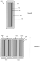
- FIG 9 shows a radial cross section through a ReBCO tape 900 that is similar to the ReBCO tape 100 of Figure 1 .
- Elements which are the same as in the tape of Fig. 1 are given the same reference numerals.
- the copper stabilizer layer 105 and the silver layer 104 can be seen to extend around the other layers of the tape 900 to enclose them completely, i.e. the copper stabilizer layer 105 and silver layer 104 act as cladding for the layered structure of the tape 900.
- the substrate 101 is typically Hastelloy TM and has a thickness of around 50-75 ⁇ m.
- the buffer stack 102 is a series of four ceramic layers of materials such as MgO, LaMaO3, YSZ, etc. which typically have a combined thickness of around several hundred nanometres to a few microns. Details of the composition and thickness of the layers of the buffer stack 102 generally vary according to supplier.
- the copper cladding 105 is typically around 10 to 20 ⁇ m thick (including at the edges). Buffer stacks with more than (or fewer than) four ceramic layers could also be used.
- Figure 10 shows a radial cross section view of a pancake coil 1000 formed by winding two ReBCO tapes 900A,B about an axis Z (the axis of the coil).
- the windings 1002, 1004 of the coil 1000 are nested within one another to form a generally planar coil 1000.
- the tapes 900A,B are arranged in a type-0 configuration, such that their ReBCO layers face one another, which allows some electrical current to be shared between the two tapes 900A,B when the coil 1000 is operated.
- Other configurations are of course possible, as discussed above.
- the coil 1000 is generally solder potted with e.g. PbSn solder, to form a non-insulated coil.
- Figure 11 shows a radial cross section view of a coil 1100 made by removing the copper and silver cladding 104, 105 from both faces of coil 1000 to expose the layered structure of the ReBCO tape 900.
- the cladding can be removed mechanically by several methods, including turning or wire erosion.
- a copper plate is soldered across a face of the coil 1000 and the plate subsequently machined away by milling, grinding, turning (e.g. on a lathe), or other means of mechanical metal removal, to leave one or more metal joint rings for injecting current into the coil 1000 through the edges of the HTS tapes 900A,B.
- the cutting tool penetrates the metal plate and continues into the HTS tapes 900A,B to remove around 0.5 mm of the edges of the HTS tapes 900A,B.
- This process can of course be carried out on one or both of the faces of the coil 1000, depending on the desired turn-to-turn resistance for the coil 1000 (which is maximised by removing the cladding entirely from both faces).
- the turn-to-turn resistance can also be varied by changing the thickness of one or more of the layers 104 of the buffer stack of the HTS tapes 900A,B (e.g. a thinner buffer stack can be used to make a coil that is only partially insulating).
- Other types of metal plate other than copper
- Current can also be injected into the coil by means other than an "edge connected" plate. For example, metallic components (contacts) at the inner diameter and/or the outer diameter of the coil onto which the cable is terminated e.g. by soldering.
- Figure 13 shows a radial cross section view of a coil 1300 comprising a plurality of windings of HTS tape 1301 arranged to form a predominantly planar pancake coil and two ring conductors 1303A, B covering the faces of the coil across the edges of the HTS tape 1301 on either side of the coil 1300.
- Each ring conductor 1303A,B comprises an annulus or ring made from a conducting material, preferably a metal such as copper, which extends radially across the coil to form an electrical connection between the windings of the coil 1300.
- the ring conductors 1303A,B are soldered to faces of the coil 1300 to provide good electrical contact with the edges of the HTS tape 1301.
- Figure 14 shows a radial cross section view of a coil 1400 obtained by removing the ring conductors 1303A,B and the cladding 105 from a portion of the coil 1300 shown in Figure 13 .
- material from the ring conductor and the cladding can be machined away to leave portions of the ring conductors 1403A,B bonded to the cladding 105, whilst exposing the HTS layer 103 at the edge of the HTS tape 1401.
- Electric current can be supplied to the coil 1400 through the radially innermost end of the HTS tape 1401 using the top ring conductor 1403A.
- the current distribution within the coil 1400 then adjusts from a distribution that (i) initially reduces the inductive voltage (such that the current flows from the radially outermost edge of the top ring conductor 1403A through the turns of the coil 900 in between the two ring conductors 1403A,B and out through the radially innermost edge of the bottom ring conductor 1403B) to (ii) a current distribution that minimises Ohmic voltage (such that current will penetrate all the turns of the ring conductors 1403A,B evenly).
- a BLI coil may also be formed by removing the metal cladding from the sides of the HTS tape before winding the coil.
- the coils 1000, 1100, 1200, 1300, 1400 described above are wound from a cable formed from two HTS tapes arranged in a type-0 configuration (with the HTS layers facing each other), which allows electrical current to be shared between the two HTS tapes 900A,B.
- Coils may also be formed from cable comprising more than two HTS tapes 900A,B.
- removing the copper 105 and silver 104 cladding from the axial edges of the tapes 900A,B may prevent electrical current being shared between all the tapes 900A,B in the cable. This is because removal of the cladding means that current is only shared between tapes for which there is a type-0 configuration, i.e. for which the HTS layers 103 face one another.
- a solution to this problem may be achieved by winding the coil from cable comprising HTS tapes of different widths, as described below.
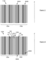
- Figure 15 shows a radial cross section of a coil 1500 that comprises windings 1502, 1504 of a cable comprising four HTS tapes 1501A-D.
- the central axis Z of the coil (not shown) is to the right of part of the coil illustrated in Figure 15 .
- Two of the tapes 1501A, D have a width that is greater than the width of the other two tapes 1501B,C.
- the "widths" of the tapes 1501A-D i.e. the second shortest dimension of the tapes
- Figures 15 and 16 show radial cross sections through the coils.
- Each of the narrower tapes 1501B,C is provided in the cable between the wider tapes 1501A,D and arranged in a type-0 configuration with a respective one of the wider tapes 1501A,D, i.e. the wider tapes 1501A,D are oriented such that their HTS layers 103 are closer to the centre of the cable than their buffer stacks 102, while the narrower tapes 901B,C are orientated such that their HTS layers 103 are further from the centre of the cable than their buffer stacks 102.
- the windings of the coil 1500 are aligned on one side 1506A of the coil 1500 (in the direction transverse to the radial and circumferential directions) to give the coil a flat face on this (bottom) side 1506A of the coil 1500 and a radially "crenelated" face on the other (top) side 1506B of the coil 1500 as a result of the wider tapes 1501A,D protruding from the coil 1500 relative to the narrower tapes 1501B,C.
- the silver cladding 104 and the copper cladding 105 in the coil 1500 is intact.
- Figure 16 shows a radial cross section of a coil 1600 obtained by removing the silver cladding 104 and copper cladding 105 from the flat face of the coil 1000 on the bottom side 1006B of the coil 1500 and from the wider tapes 1501A,D on the top side 1506B of the coil ("narrower” and “wider” referring here to the extent of the tapes along the axis of the coil 1600) .
- the cladding 104, 105 of the narrow tapes 1501B,C is not removed on the top side 1506B.
- the coil 1600 is a BLI coil.
- the coil 1500 may not have the edges of the HTS tapes aligned on one side 1506A, i.e. both sides of the coil 1500 may be stepped or "crenelated", in which case, is may not be necessary to remove any of the cladding 104, 105 from the narrower HTS tapes 1501B,C.
- the coil 1500 may be "potted" with solder to fill in the gaps between the wider tapes 1501A,D as this facilitates removal of the cladding 104, 105 from the wider tapes 1501A, D on the top side 1506B of the coil 1500.
- the solder covering the narrower tapes 1501BC provides mechanical stability for the wider tapes 1501A,D along the radial direction, which prevents them being damaged when the top side 1506B of the coil 1500 is machined to remove the cladding 104, 105.
- the wider tapes 1501A,D have a width of 12 mm whereas the narrower tapes 1501B,C have a width of 11 mm or 10 mm.
- the HTS layer 103 and buffer stack 102 of the wider tapes 1501A,D should extend above the narrower tapes 1501B,C so that the cladding 104, 105 can be removed from the wider tapes 1501A,D without damaging the cladding 104, 105 of the narrower tape 1001B,C.
- the cladding 104, 105 of the tapes 1500A-D may extend beyond the HTS layer 103 and the buffer stack 102 by around 10 micrometers, such that around 10 micrometers of material (i.e.
- cladding would need to be removed from either face of the coil 1500 to produce an insulated coil 1600.
- variation in the width of the HTS tape width and the alignment of the windings with respect to one another i.e. the flatness of the coil
- FIG 17 is a flowchart of a method of manufacturing an HTS coil from one or more HTS tapes.
- Each HTS tape comprises a flexible substrate, an electrical insulator layer (e.g. a buffer stack 102) provided on a face of the flexible substrate, an HTS material layer provided on the electrical insulator layer, and electrically conductive cladding in electrical contact with the HTS material and extending across at least an edge of the HTS tape.
- the electrical insulator layer may be only "partially insulating", in which case the electrical insulator may, for example, have a resistivity between 100 and 10 16 times that of copper or between 10 -6 and 10 8 Ohm metre, and so forth.
- the electrical current may continue to be able to circulate around the HTS material of such coils even when there are interruptions to or damage within some of the coil windings. This may occur as a result of current sharing between neighbouring windings, which allows the current to "bypass" the affected parts of the windings.
- Current may continue to circulate around the windings of the coil so long as the total current does not exceed the minimum critical current of the HTS material in any part of the coil, or potentially even beyond the minimum critical current if the turn to turn resistance is sufficiently low and cooling is provided to cool the resistive heat load.
- reduced width HTS field coils may be made by cutting through the HTS field coil, e.g. by cutting across the HTS field coil 1000, 1100, 1200 in a plane that is perpendicular to the coil axis Z, thereby dividing the coil into two HTS field coils of reduced width.
- the plane may bisect the field coil 1000, 1100, 1200 so that each of the narrower field coils has a width that is approximately half that of the original field coil 1000, 1100, 1200.
- one or more 12 mm wide HTS tapes may be wound into a pancake coil, which is then divided into two pancake coils each having a width of approximately 6 mm.
- the axial edges (or potentially all the outer surfaces) of the HTS field coils may preferably be hermetically sealed to prevent ingress of contaminants into the exposed laminar structure. This can be done by applying an insulator coating such as a ceramic or resin (e.g. epoxy resin). An insulating coating may be preferred to avoid forming unwanted electrical connections between turns. However, in some cases, such as where the HTS field have a low turn-to-turn resistivity (e.g. "partially insulated" coils), one or more metal layers may be applied instead (or applied beneath the insulator coating) to protect the layers of the HTS tape. For example a layer of nickel may be applied to the HTS coils, e.g. by deposition onto the surfaces of the HTS field coils via electroplating or other chemical or physical deposition methods.
- an insulator coating such as a ceramic or resin (e.g. epoxy resin).
- An insulating coating may be preferred to avoid forming unwanted electrical connections between turns.
- one or more metal layers may be applied instead
- Figure 20 shows results of a stress simulation of a cross section 2001 of a TF magnet, showing the windings of HTS tape 2002 of a single pancake coil which has had an incline 2003 cut into it. Comparing this to Figure 19 , it can be seen that the stress is considerably reduced - being less than 330 MPa throughout the structure.
- HTS coils While the above examples have been directed towards TF coils in tokamaks, it will be appreciated that the technique of cutting and shaping HTS coils may be applied to any application of HTS coils, and is particularly useful in applications where the space available for the coils is limited and/or irregularly shaped, e.g. in aircraft and/or spacecraft. Also, while the above description has focussed on pancake coils, the method applies equally to other partially- or non-insulated coil constructions, e.g. jointed coils.
- the HTS field coils described above are particularly advantageous for use in aerospace applications.
- the HTS field coils may be included in aircraft, unmanned aerial vehicles, satellites, spacecraft, rocket-propelled vehicles, and autonomous exploration vehicles.
- removing material from an axial edge of the one or more of the HTS tapes allows the shape of the coil to be adapted so that it takes up less volume and is lighter. This is particularly beneficial for technologies in which there are space and weight constraints, such as in satellites.
- Buffer layer insulated HTS field coils are also advantageous in this regard because they are able to provide partially insulated (PI) or fully insulated coils without requiring additional layers of insulating material to be introduced between the windings, therefore further reducing the volume/weight of the coils.
- the HTS tapes are generally unmodified when the HTS field coils are wound (with the material then being removed after winding), it is possible to form tightly wound, consolidated coils, which are able to withstand large forces, such as those generated during take-off of an aircraft or launch of a satellite and so forth.
- producing HTS field coils with a high degree of mechanical stability is generally more difficult using other manufacturing methods in which material is removed from the HTS tapes before the coil is wound, or which require additional layers to be introduced between the windings.
- HTS field coils may, in general, be provided to generate a magnetic field that has a particular strength and spatial distribution. However, in some cases, it is possible to remove material from the axial edge of the one or more of the HTS tapes to reduce the size and mass of the coil, whilst largely preserving the strength and/or spatial distribution generated by the coil.
- the amount and/or location of the material to be removed may be determined by trial and error, or preferably from computer simulations (e.g. finite element models) of the coils and their associated magnetic field. In the latter case, evolutionary or genetic algorithms may be used to optimise the removal of the material. These algorithms may, for example, be subject to one or more constraints (e.g. acceptable tolerances) relating to the strength and spatial distribution of the magnetic field and/or the operating parameters of the coil, such as current and temperature.
- the shape of the HTS field coils may also (or alternatively) be varied by removing material from the HTS tapes to obtain a particular current distribution within the tapes when the coil is in use.
- the material may be removed from the HTS tapes (e.g. by machining the coil), so that the ratio of the current to the critical current (I/ I C ) is approximately constant for a particular region of the coil or throughout the coil.
- This kind of optimisation may reduce the "excess" current (i.e. the current exceeding the critical current) and allow the coil to be operated in a "saturated" mode in which the current is substantially equal to the critical current to minimise resistive heating within the coil.
- HTS pancake coil that has been divided into two or more HTS field coils of reduced width, i.e. reduced extent along the axis of the coil (see the discussion above of reduced width HTS field coils), e.g. by "wire slicing" a pancake coil into two smaller (reduced width) pancake coils.
- a further benefit associated with coils manufactured this way is that the electrical current required from a power supply is reduced, thereby allowing a smaller and/or lighter power supply and non-superconducting current carrying components to be used.
- the reduced power consumption of the HTS field coils may also extend the lifetime of the power supply, which may be an electrochemical cell (battery), for example.
- the technique used for removing material from an HTS field coil may, in some cases, be selected depending on the application for which the HTS coil is to be used. Generally, however, any of the techniques described above can be used, such as EDM, grinding, sanding, etching, laser cutting, plasma cutting, water jet cutting, chemically removing the material, etc.
Landscapes
- Engineering & Computer Science (AREA)
- Power Engineering (AREA)
- Physics & Mathematics (AREA)
- Plasma & Fusion (AREA)
- General Engineering & Computer Science (AREA)
- High Energy & Nuclear Physics (AREA)
- Manufacturing & Machinery (AREA)
- Superconductors And Manufacturing Methods Therefor (AREA)
Claims (15)
- Verfahren zum Herstellen einer Hochtemperatur-Supraleiter-(HTS-)Feldspule (1100, 1400) aus einem oder mehreren HTS-Bändern (100, 900, 900A, B, 1401, 1501A-D), wobei jedes HTS-Band ein flexibles Substrat, eine auf einer Fläche des flexiblen Substrats vorgesehene Zwischenschicht (102), eine auf der Zwischenschicht vorgesehene HTS-Materialschicht (103) und eine elektrisch leitende Plattierung (104, 105) umfasst, die in elektrischem Kontakt mit dem HTS-Material ist und sich über mindestens die Kanten des HTS-Bands erstreckt, wobei das Verfahren Folgendes umfasst:Wickeln (2201) des einen oder der mehreren HTS-Bänder um eine Achse (Z), um eine Feldspule (1000, 1300) zu bilden, die Wicklungen (1002, 1004) aus HTS-Band umfasst; undgekennzeichnet durch:
nach dem Wickeln, Entfernen (2203) von Material von einer axialen Kante des einen oder der mehreren HTS-Bänder um mindestens einen Teil von einer oder mehreren der Wicklungen, um die Ausdehnung des einen oder der mehreren HTS-Bänder entlang der Achse der Feldspule zu verringern, wobei das Entfernen von Material von einer axialen Kante des einen oder der mehreren der HTS-Bänder ein partielles oder vollständiges Entfernen der Plattierung von einer Kante des einen oder der mehreren der HTS-Bänder um mindestens einen Teil von einer oder mehreren der Wicklungen umfasst, um den elektrischen Widerstand zwischen der HTS-Materialschicht in der Wicklung und der HTS-Materialschicht in einer angrenzenden Wicklung zu erhöhen. - Verfahren nach Anspruch 1, wobei das Entfernen (2203) von Material von der axialen Kante des einen oder der mehreren HTS-Bänder (100, 900, 900A,B, 1401, 1501A-D) ein Verringern einer Ausdehnung der HTS-Materialschicht (103) entlang der Achse der Feldspule (1000, 1300) umfasst.
- Verfahren nach Anspruch 1 oder 2, wobei das Entfernen der Plattierung (104, 105) von der Kante von einem oder mehreren der HTS-Bänder (100, 900, 900A, B, 1401, 1501A-D) ein Entfernen der Plattierung zum Freilegen der HTS-Materialschicht an einer axialen Kante des einen oder der mehreren der HTS-Bänder um den mindestens einen Teil von einer oder mehreren der Wicklungen umfasst.
- Verfahren nach einem der vorhergehenden Ansprüche, wobei das Material von der Kante des einen oder der mehreren HTS-Bänder (100, 900, 900A, B, 1401, 1501A- D) über eine Gesamtheit einer Fläche der Feldspule (1000, 1300) entfernt wird.
- Verfahren nach einem der vorhergehenden Ansprüche, ferner umfassend ein Abdichten der Kante des einen oder der mehreren der HTS-Bänder (100, 900, 900A, B, 1401, 1501A-D) mit einem Isolier- oder Leitermaterial.
- Verfahren nach einem der vorhergehenden Ansprüche und umfassend ein Kühlen der HTS-Feldspule (1000, 1300) während des Schritts des Entfernens des Materials von der axialen Kante des einen oder der mehreren HTS-Bänder (100, 900, 900A, B, 1401, 1501A-D).
- Verfahren nach einem der vorhergehenden Ansprüche, umfassend vor dem Entfernen von Material von der axialen Kante des einen oder der mehreren der HTS-Bänder (100, 900, 900A, B, 1501A-D) ein Vergießen der Feldspule (1000, 1300).
- Verfahren nach einem der vorhergehenden Ansprüche, wobei das Entfernen des Materials ein Schneiden durch die HTS-Feldspule (1000, 1300) umfasst, um die HTS-Feldspule in zwei oder mehr HTS-Feldspulen (1100, 1400) zu unterteilen.
- Verfahren nach einem der vorhergehenden Ansprüche, wobei das Wickeln des einen oder der mehreren HTS-Bänder (100, 900, 900A,B, 1401, 1501A-D) um eine Achse, um eine Feldspule (1100, 1400) zu bilden, ein Wickeln eines Kabels mit zwei äußeren HTS-Bändern (1501A,D) des einen oder der mehreren HTS-Bänder und einem oder mehreren inneren HTS-Bändern (1501B, C) umfasst, wobei das innere bzw. die inneren HTS-Bänder zwischen den äußeren HTS-Bändern angeordnet sind und eine Metallplattierung (104, 105) aufweisen, die einen elektrisch leitenden Weg zwischen den HTS-Schichten der zwei äußeren HTS-Bänder bereitstellt.
- Verfahren nach Anspruch 9, wobei vor dem Entfernen des Materials die Ausdehnung des bzw. der inneren HTS-Bänder (1501B, C) entlang der Achse der Spule (1000, 1300) geringer als die Ausdehnung der äußeren HTS-Bänder (1501A, D) entlang der Achse (Z) der Spule ist.
- Verfahren nach Anspruch 10, wobei vor dem Entfernen des Materials jeweilige axiale Kanten des bzw. der inneren HTS-Bänder (1501B, C) und der äußeren HTS-Bänder (1501A, D) entlang einer Kante des Kabels aufeinander ausgerichtet sind.
- Verfahren zum Herstellen eines Elektromagneten, wobei der Elektromagnet eine Hochtemperatur-Supraleiter-(HTS-)Feldspule umfasst, die innerhalb einer Aussparung oder eines geschlossenen Raums installiert ist, wobei das Verfahren Folgendes umfasst:Herstellen einer HTS-Feldspule (1100, 1400) gemäß dem Verfahren nach einem der vorhergehenden Ansprüche, wobei der Schritt des Entfernens von Material von der axialen Kante des einen oder der mehreren HTS-Bänder (100, 900, 900A, B, 1401, 1501A-D) der HTS-Feldspule ein Entfernen des Materials umfasst, um die HTS-Feldspule (1000, 1300) so anzupassen, dass sie in die Aussparung oder den geschlossenen Raum passt; undInstallieren der HTS-Feldspule (1100, 1400) in die Aussparung oder den geschlossenen Raum.
- Verfahren zur Herstellung eines Ringfeld-(RF-)Magneten, umfassend eine Vielzahl von Hochtemperatur-Supraleiter-(HTS-)-Feldspulen zur Verwendung in einer Tokamak-Plasmakammer, wobei das Verfahren Folgendes umfasst:Herstellen einer Vielzahl von HTS-Feldspulen gemäß dem Verfahren nach einem der Ansprüche 1 bis 11, wobei jede der HTS-Feldspulen einen Abschnitt zum Installieren in einen jeweiligen Sektor einer Mittelsäule des RF-Magneten umfasst, und wobei der Schritt des Entfernens von Material von der axialen Kante des einen oder der mehreren HTS-Bänder (100, 900, 900A,B, 1401, 1501A- D) jeder HTS-Feldspule ein Entfernen des Materials umfasst, um einen Querschnitt des Abschnitts der HTS-Feldspule an einen Querschnitt des Sektors anzupassen;Installieren des Abschnitts jeder HTS-Feldspule in seinen jeweiligen Sektor; undAnordnen der Sektoren um eine Mittelachse, um die Mittelsäule des RF-Magneten zu bilden, wobei die Wicklungen innerhalb der Abschnitte der in die Sektoren installierten HTS-Feldspulen parallel zur Mittelachse angeordnet sind.
- Hochtemperatur-Supraleiter-(HTS-)Feldspule, die gemäß dem Verfahren nach einem der Ansprüche 1 bis 11 hergestellt ist.
- HTS-Feldspule nach Anspruch 14, umfassend ein elektrisches Isoliermaterial, das auf einer oder mehreren axialen Kanten des einen oder der mehreren HTS-Bänder (100, 900, 900A, B, 1401, 1501A-D) vorgesehen ist.
Priority Applications (1)
| Application Number | Priority Date | Filing Date | Title |
|---|---|---|---|
| EP25160901.2A EP4539062A3 (de) | 2020-05-04 | 2021-05-04 | Hochtemperatur-supraleiter-feldspule |
Applications Claiming Priority (2)
| Application Number | Priority Date | Filing Date | Title |
|---|---|---|---|
| GBGB2006576.9A GB202006576D0 (en) | 2020-05-04 | 2020-05-04 | High temperature superconductor field coil |
| PCT/EP2021/061756 WO2021224279A1 (en) | 2020-05-04 | 2021-05-04 | High temperature superconductor field coil |
Related Child Applications (2)
| Application Number | Title | Priority Date | Filing Date |
|---|---|---|---|
| EP25160901.2A Division EP4539062A3 (de) | 2020-05-04 | 2021-05-04 | Hochtemperatur-supraleiter-feldspule |
| EP25160901.2A Division-Into EP4539062A3 (de) | 2020-05-04 | 2021-05-04 | Hochtemperatur-supraleiter-feldspule |
Publications (2)
| Publication Number | Publication Date |
|---|---|
| EP4147281A1 EP4147281A1 (de) | 2023-03-15 |
| EP4147281B1 true EP4147281B1 (de) | 2025-04-09 |
Family
ID=71080529
Family Applications (2)
| Application Number | Title | Priority Date | Filing Date |
|---|---|---|---|
| EP25160901.2A Pending EP4539062A3 (de) | 2020-05-04 | 2021-05-04 | Hochtemperatur-supraleiter-feldspule |
| EP21723965.6A Active EP4147281B1 (de) | 2020-05-04 | 2021-05-04 | Ein verfahren zur herstellung einer hochtemperatur-supraleiter-feldspule und einehochtemperatur-supraleiter-feldspule |
Family Applications Before (1)
| Application Number | Title | Priority Date | Filing Date |
|---|---|---|---|
| EP25160901.2A Pending EP4539062A3 (de) | 2020-05-04 | 2021-05-04 | Hochtemperatur-supraleiter-feldspule |
Country Status (9)
| Country | Link |
|---|---|
| US (1) | US20230343498A1 (de) |
| EP (2) | EP4539062A3 (de) |
| JP (2) | JP7734149B2 (de) |
| KR (2) | KR102898625B1 (de) |
| CN (1) | CN115485868B (de) |
| AU (1) | AU2021266593A1 (de) |
| CA (1) | CA3177628A1 (de) |
| GB (1) | GB202006576D0 (de) |
| WO (1) | WO2021224279A1 (de) |
Families Citing this family (6)
| Publication number | Priority date | Publication date | Assignee | Title |
|---|---|---|---|---|
| GB202205209D0 (en) | 2022-04-08 | 2022-05-25 | Tokamak Energy Ltd | Hts tape with improved transverse conductance |
| GB2631528A (en) | 2023-07-06 | 2025-01-08 | Tokamak Energy Ltd | Superconducting magnet arrangement |
| KR102876094B1 (ko) * | 2024-05-27 | 2025-10-27 | 한국핵융합에너지연구원 | 스택 기반 고온초전도 조인트, 전류 리드, 스택-인-도관 도체 및 자석 |
| CN118380168B (zh) * | 2024-06-25 | 2024-09-06 | 中国科学院合肥物质科学研究院 | 一种中性束注入功率反馈控制方法 |
| CN118888253B (zh) * | 2024-07-16 | 2025-06-27 | 华中科技大学 | 一种单匝线圈式破坏性脉冲磁体 |
| EP4703754A1 (de) * | 2024-08-28 | 2026-03-04 | Siemens Healthcare Limited | Magnetanordnung und herstellungsverfahren |
Citations (3)
| Publication number | Priority date | Publication date | Assignee | Title |
|---|---|---|---|---|
| WO2019150123A1 (en) * | 2018-02-01 | 2019-08-08 | Tokamak Energy Ltd | Partially-insulated hts coils |
| WO2020104807A1 (en) * | 2018-11-22 | 2020-05-28 | Tokamak Energy Ltd | Rapid dump of partially insulated superconducting magnet |
| EP4078630A1 (de) * | 2019-12-20 | 2022-10-26 | Tokamak Energy Ltd | Hts-verknüpfte teilisolierung für hts-feldspulen |
Family Cites Families (18)
| Publication number | Priority date | Publication date | Assignee | Title |
|---|---|---|---|---|
| US3665351A (en) * | 1970-07-09 | 1972-05-23 | Gen Electric | Superconductive magnets |
| JPS5912004B2 (ja) * | 1976-07-05 | 1984-03-19 | 誠 桂井 | 準超電導方式コイル |
| JP3120626B2 (ja) * | 1993-04-28 | 2000-12-25 | 日立電線株式会社 | 酸化物超電導導体 |
| US6765151B2 (en) * | 1999-07-23 | 2004-07-20 | American Superconductor Corporation | Enhanced high temperature coated superconductors |
| AU1325101A (en) * | 1999-07-23 | 2001-02-13 | American Superconductor Corporation | Multi-layer articles and methods of making same |
| US7816303B2 (en) | 2004-10-01 | 2010-10-19 | American Superconductor Corporation | Architecture for high temperature superconductor wire |
| KR100720057B1 (ko) * | 2005-07-06 | 2007-05-18 | 학교법인 한국산업기술대학 | 영구전류용 초전도자석 및 제조방법 |
| GB0519882D0 (en) * | 2005-09-29 | 2005-11-09 | Oxford Instr Superconductivity | Superconducting electromagnet |
| KR100964354B1 (ko) * | 2008-08-04 | 2010-06-18 | 케이조인스(주) | 초전도체층의 직접 용융확산에 의한 2세대 초전도 선재의접합방법 |
| US8716188B2 (en) | 2010-09-15 | 2014-05-06 | Superpower, Inc. | Structure to reduce electroplated stabilizer content |
| US9852816B2 (en) | 2011-09-02 | 2017-12-26 | Tokamak Energy Ltd | Efficient compact fusion reactor |
| GB2510447B (en) * | 2013-09-13 | 2015-02-18 | Tokamak Energy Ltd | Toroidal field coil for use in a fusion reactor |
| DE102014206506A1 (de) * | 2014-04-04 | 2015-10-08 | Siemens Aktiengesellschaft | Elektrische Spuleneinrichtung mit wenigstens zwei Teilspulen und Verfahren zur Herstellung |
| US11309480B2 (en) * | 2015-05-11 | 2022-04-19 | University Of Houston System | Ultra-thin film superconducting tapes |
| KR102683995B1 (ko) * | 2016-01-21 | 2024-07-12 | 브룩해븐 테크놀로지 그룹, 인크. | 제2세대 초전도성 필라멘트와 케이블 |
| GB201618334D0 (en) | 2016-10-31 | 2016-12-14 | Tokamak Energy Ltd | Cable design in hts tokamaks |
| US11146116B2 (en) * | 2017-08-17 | 2021-10-12 | Columbiad Launch Services Inc. | System and method for distributing power to aircraft systems |
| SG11202103543TA (en) * | 2018-10-15 | 2021-05-28 | Tokamak Energy Ltd | High temperature superconductor magnet |
-
2020
- 2020-05-04 GB GBGB2006576.9A patent/GB202006576D0/en not_active Ceased
-
2021
- 2021-05-04 KR KR1020227040959A patent/KR102898625B1/ko active Active
- 2021-05-04 KR KR1020257040909A patent/KR20250175012A/ko active Pending
- 2021-05-04 JP JP2022566609A patent/JP7734149B2/ja active Active
- 2021-05-04 EP EP25160901.2A patent/EP4539062A3/de active Pending
- 2021-05-04 WO PCT/EP2021/061756 patent/WO2021224279A1/en not_active Ceased
- 2021-05-04 AU AU2021266593A patent/AU2021266593A1/en active Pending
- 2021-05-04 CN CN202180032673.3A patent/CN115485868B/zh active Active
- 2021-05-04 EP EP21723965.6A patent/EP4147281B1/de active Active
- 2021-05-04 US US17/997,798 patent/US20230343498A1/en active Pending
- 2021-05-04 CA CA3177628A patent/CA3177628A1/en active Pending
-
2025
- 2025-08-25 JP JP2025139443A patent/JP2026000905A/ja active Pending
Patent Citations (3)
| Publication number | Priority date | Publication date | Assignee | Title |
|---|---|---|---|---|
| WO2019150123A1 (en) * | 2018-02-01 | 2019-08-08 | Tokamak Energy Ltd | Partially-insulated hts coils |
| WO2020104807A1 (en) * | 2018-11-22 | 2020-05-28 | Tokamak Energy Ltd | Rapid dump of partially insulated superconducting magnet |
| EP4078630A1 (de) * | 2019-12-20 | 2022-10-26 | Tokamak Energy Ltd | Hts-verknüpfte teilisolierung für hts-feldspulen |
Also Published As
| Publication number | Publication date |
|---|---|
| WO2021224279A1 (en) | 2021-11-11 |
| KR20250175012A (ko) | 2025-12-15 |
| AU2021266593A1 (en) | 2022-12-01 |
| US20230343498A1 (en) | 2023-10-26 |
| GB202006576D0 (en) | 2020-06-17 |
| JP2023525694A (ja) | 2023-06-19 |
| EP4147281A1 (de) | 2023-03-15 |
| EP4539062A3 (de) | 2025-07-23 |
| CN115485868B (zh) | 2026-04-07 |
| KR20230005275A (ko) | 2023-01-09 |
| JP2026000905A (ja) | 2026-01-06 |
| CA3177628A1 (en) | 2021-11-11 |
| CN115485868A (zh) | 2022-12-16 |
| JP7734149B2 (ja) | 2025-09-04 |
| EP4539062A2 (de) | 2025-04-16 |
| KR102898625B1 (ko) | 2025-12-09 |
Similar Documents
| Publication | Publication Date | Title |
|---|---|---|
| EP4539062A2 (de) | Hochtemperatur-supraleiter-feldspule | |
| US12586702B2 (en) | High temperature superconductor magnet | |
| US11289253B2 (en) | Wound HTS magnet coils | |
| AU2019214510A1 (en) | Partially-insulated HTS coils | |
| JP7754953B2 (ja) | トカマクプラズマチャンバ用の中心柱 | |
| RU2843604C1 (ru) | Катушка возбуждения с высокотемпературным сверхпроводником | |
| WO2024118671A9 (en) | High-temperature superconductor magnets with quench damage resiliency | |
| EP4285395B1 (de) | Verbindungsschemata für gestapelte platten und nichtisolierte supraleitende magnete | |
| HK40047607B (en) | High temperature superconductor magnet | |
| HK40047607A (en) | High temperature superconductor magnet |
Legal Events
| Date | Code | Title | Description |
|---|---|---|---|
| STAA | Information on the status of an ep patent application or granted ep patent |
Free format text: STATUS: UNKNOWN |
|
| STAA | Information on the status of an ep patent application or granted ep patent |
Free format text: STATUS: THE INTERNATIONAL PUBLICATION HAS BEEN MADE |
|
| PUAI | Public reference made under article 153(3) epc to a published international application that has entered the european phase |
Free format text: ORIGINAL CODE: 0009012 |
|
| STAA | Information on the status of an ep patent application or granted ep patent |
Free format text: STATUS: REQUEST FOR EXAMINATION WAS MADE |
|
| 17P | Request for examination filed |
Effective date: 20221122 |
|
| AK | Designated contracting states |
Kind code of ref document: A1 Designated state(s): AL AT BE BG CH CY CZ DE DK EE ES FI FR GB GR HR HU IE IS IT LI LT LU LV MC MK MT NL NO PL PT RO RS SE SI SK SM TR |
|
| P01 | Opt-out of the competence of the unified patent court (upc) registered |
Effective date: 20230512 |
|
| DAV | Request for validation of the european patent (deleted) | ||
| DAX | Request for extension of the european patent (deleted) | ||
| STAA | Information on the status of an ep patent application or granted ep patent |
Free format text: STATUS: EXAMINATION IS IN PROGRESS |
|
| 17Q | First examination report despatched |
Effective date: 20231219 |
|
| REG | Reference to a national code |
Ref country code: DE Ref legal event code: R079 Free format text: PREVIOUS MAIN CLASS: H01L0039240000 Ipc: H01F0041040000 Ref country code: DE Ref legal event code: R079 Ref document number: 602021028899 Country of ref document: DE Free format text: PREVIOUS MAIN CLASS: H01L0039240000 Ipc: H01F0041040000 |
|
| RIC1 | Information provided on ipc code assigned before grant |
Ipc: H01F 6/06 20060101ALI20240828BHEP Ipc: H01F 41/04 20060101AFI20240828BHEP |
|
| GRAP | Despatch of communication of intention to grant a patent |
Free format text: ORIGINAL CODE: EPIDOSNIGR1 |
|
| STAA | Information on the status of an ep patent application or granted ep patent |
Free format text: STATUS: GRANT OF PATENT IS INTENDED |
|
| RIC1 | Information provided on ipc code assigned before grant |
Ipc: G21B 1/11 20060101ALI20241002BHEP Ipc: G21B 1/05 20060101ALI20241002BHEP Ipc: H01F 6/06 20060101ALI20241002BHEP Ipc: H01F 41/04 20060101AFI20241002BHEP |
|
| INTG | Intention to grant announced |
Effective date: 20241031 |
|
| GRAS | Grant fee paid |
Free format text: ORIGINAL CODE: EPIDOSNIGR3 |
|
| GRAA | (expected) grant |
Free format text: ORIGINAL CODE: 0009210 |
|
| STAA | Information on the status of an ep patent application or granted ep patent |
Free format text: STATUS: THE PATENT HAS BEEN GRANTED |
|
| AK | Designated contracting states |
Kind code of ref document: B1 Designated state(s): AL AT BE BG CH CY CZ DE DK EE ES FI FR GB GR HR HU IE IS IT LI LT LU LV MC MK MT NL NO PL PT RO RS SE SI SK SM TR |
|
| REG | Reference to a national code |
Ref country code: GB Ref legal event code: FG4D |
|
| REG | Reference to a national code |
Ref country code: CH Ref legal event code: EP |
|
| REG | Reference to a national code |
Ref country code: DE Ref legal event code: R096 Ref document number: 602021028899 Country of ref document: DE |
|
| REG | Reference to a national code |
Ref country code: IE Ref legal event code: FG4D |
|
| PGFP | Annual fee paid to national office [announced via postgrant information from national office to epo] |
Ref country code: DE Payment date: 20250521 Year of fee payment: 5 |
|
| PGFP | Annual fee paid to national office [announced via postgrant information from national office to epo] |
Ref country code: GB Payment date: 20250527 Year of fee payment: 5 |
|
| PGFP | Annual fee paid to national office [announced via postgrant information from national office to epo] |
Ref country code: FR Payment date: 20250603 Year of fee payment: 5 |
|
| PGFP | Annual fee paid to national office [announced via postgrant information from national office to epo] |
Ref country code: CH Payment date: 20250601 Year of fee payment: 5 |
|
| PGFP | Annual fee paid to national office [announced via postgrant information from national office to epo] |
Ref country code: AT Payment date: 20250721 Year of fee payment: 5 |
|
| REG | Reference to a national code |
Ref country code: NL Ref legal event code: MP Effective date: 20250409 |
|
| PG25 | Lapsed in a contracting state [announced via postgrant information from national office to epo] |
Ref country code: NL Free format text: LAPSE BECAUSE OF FAILURE TO SUBMIT A TRANSLATION OF THE DESCRIPTION OR TO PAY THE FEE WITHIN THE PRESCRIBED TIME-LIMIT Effective date: 20250409 |
|
| REG | Reference to a national code |
Ref country code: AT Ref legal event code: MK05 Ref document number: 1784340 Country of ref document: AT Kind code of ref document: T Effective date: 20250409 |
|
| PG25 | Lapsed in a contracting state [announced via postgrant information from national office to epo] |
Ref country code: PT Free format text: LAPSE BECAUSE OF FAILURE TO SUBMIT A TRANSLATION OF THE DESCRIPTION OR TO PAY THE FEE WITHIN THE PRESCRIBED TIME-LIMIT Effective date: 20250811 Ref country code: FI Free format text: LAPSE BECAUSE OF FAILURE TO SUBMIT A TRANSLATION OF THE DESCRIPTION OR TO PAY THE FEE WITHIN THE PRESCRIBED TIME-LIMIT Effective date: 20250409 Ref country code: ES Free format text: LAPSE BECAUSE OF FAILURE TO SUBMIT A TRANSLATION OF THE DESCRIPTION OR TO PAY THE FEE WITHIN THE PRESCRIBED TIME-LIMIT Effective date: 20250409 |
|
| REG | Reference to a national code |
Ref country code: LT Ref legal event code: MG9D |
|
| PG25 | Lapsed in a contracting state [announced via postgrant information from national office to epo] |
Ref country code: NO Free format text: LAPSE BECAUSE OF FAILURE TO SUBMIT A TRANSLATION OF THE DESCRIPTION OR TO PAY THE FEE WITHIN THE PRESCRIBED TIME-LIMIT Effective date: 20250709 Ref country code: GR Free format text: LAPSE BECAUSE OF FAILURE TO SUBMIT A TRANSLATION OF THE DESCRIPTION OR TO PAY THE FEE WITHIN THE PRESCRIBED TIME-LIMIT Effective date: 20250710 |
|
| PG25 | Lapsed in a contracting state [announced via postgrant information from national office to epo] |
Ref country code: PL Free format text: LAPSE BECAUSE OF FAILURE TO SUBMIT A TRANSLATION OF THE DESCRIPTION OR TO PAY THE FEE WITHIN THE PRESCRIBED TIME-LIMIT Effective date: 20250409 |
|
| PGFP | Annual fee paid to national office [announced via postgrant information from national office to epo] |
Ref country code: IT Payment date: 20250730 Year of fee payment: 5 |
|
| PG25 | Lapsed in a contracting state [announced via postgrant information from national office to epo] |
Ref country code: BG Free format text: LAPSE BECAUSE OF FAILURE TO SUBMIT A TRANSLATION OF THE DESCRIPTION OR TO PAY THE FEE WITHIN THE PRESCRIBED TIME-LIMIT Effective date: 20250409 |
|
| PG25 | Lapsed in a contracting state [announced via postgrant information from national office to epo] |
Ref country code: HR Free format text: LAPSE BECAUSE OF FAILURE TO SUBMIT A TRANSLATION OF THE DESCRIPTION OR TO PAY THE FEE WITHIN THE PRESCRIBED TIME-LIMIT Effective date: 20250409 |
|
| PG25 | Lapsed in a contracting state [announced via postgrant information from national office to epo] |
Ref country code: AT Free format text: LAPSE BECAUSE OF FAILURE TO SUBMIT A TRANSLATION OF THE DESCRIPTION OR TO PAY THE FEE WITHIN THE PRESCRIBED TIME-LIMIT Effective date: 20250409 |
|
| PG25 | Lapsed in a contracting state [announced via postgrant information from national office to epo] |
Ref country code: RS Free format text: LAPSE BECAUSE OF FAILURE TO SUBMIT A TRANSLATION OF THE DESCRIPTION OR TO PAY THE FEE WITHIN THE PRESCRIBED TIME-LIMIT Effective date: 20250709 |
|
| PG25 | Lapsed in a contracting state [announced via postgrant information from national office to epo] |
Ref country code: IS Free format text: LAPSE BECAUSE OF FAILURE TO SUBMIT A TRANSLATION OF THE DESCRIPTION OR TO PAY THE FEE WITHIN THE PRESCRIBED TIME-LIMIT Effective date: 20250809 |
|
| PG25 | Lapsed in a contracting state [announced via postgrant information from national office to epo] |
Ref country code: LV Free format text: LAPSE BECAUSE OF FAILURE TO SUBMIT A TRANSLATION OF THE DESCRIPTION OR TO PAY THE FEE WITHIN THE PRESCRIBED TIME-LIMIT Effective date: 20250409 |
|
| REG | Reference to a national code |
Ref country code: DE Ref legal event code: R097 Ref document number: 602021028899 Country of ref document: DE |
|
| PG25 | Lapsed in a contracting state [announced via postgrant information from national office to epo] |
Ref country code: DK Free format text: LAPSE BECAUSE OF FAILURE TO SUBMIT A TRANSLATION OF THE DESCRIPTION OR TO PAY THE FEE WITHIN THE PRESCRIBED TIME-LIMIT Effective date: 20250409 Ref country code: SM Free format text: LAPSE BECAUSE OF FAILURE TO SUBMIT A TRANSLATION OF THE DESCRIPTION OR TO PAY THE FEE WITHIN THE PRESCRIBED TIME-LIMIT Effective date: 20250409 |
|
| PG25 | Lapsed in a contracting state [announced via postgrant information from national office to epo] |
Ref country code: LU Free format text: LAPSE BECAUSE OF NON-PAYMENT OF DUE FEES Effective date: 20250504 |
|
| PG25 | Lapsed in a contracting state [announced via postgrant information from national office to epo] |
Ref country code: CZ Free format text: LAPSE BECAUSE OF FAILURE TO SUBMIT A TRANSLATION OF THE DESCRIPTION OR TO PAY THE FEE WITHIN THE PRESCRIBED TIME-LIMIT Effective date: 20250409 |
|
| PG25 | Lapsed in a contracting state [announced via postgrant information from national office to epo] |
Ref country code: EE Free format text: LAPSE BECAUSE OF FAILURE TO SUBMIT A TRANSLATION OF THE DESCRIPTION OR TO PAY THE FEE WITHIN THE PRESCRIBED TIME-LIMIT Effective date: 20250409 |
|
| PG25 | Lapsed in a contracting state [announced via postgrant information from national office to epo] |
Ref country code: SK Free format text: LAPSE BECAUSE OF FAILURE TO SUBMIT A TRANSLATION OF THE DESCRIPTION OR TO PAY THE FEE WITHIN THE PRESCRIBED TIME-LIMIT Effective date: 20250409 |
|
| REG | Reference to a national code |
Ref country code: BE Ref legal event code: MM Effective date: 20250531 |
|
| PG25 | Lapsed in a contracting state [announced via postgrant information from national office to epo] |
Ref country code: MC Free format text: LAPSE BECAUSE OF FAILURE TO SUBMIT A TRANSLATION OF THE DESCRIPTION OR TO PAY THE FEE WITHIN THE PRESCRIBED TIME-LIMIT Effective date: 20250409 |
|
| PG25 | Lapsed in a contracting state [announced via postgrant information from national office to epo] |
Ref country code: RO Free format text: LAPSE BECAUSE OF FAILURE TO SUBMIT A TRANSLATION OF THE DESCRIPTION OR TO PAY THE FEE WITHIN THE PRESCRIBED TIME-LIMIT Effective date: 20250409 |
|
| PLBE | No opposition filed within time limit |
Free format text: ORIGINAL CODE: 0009261 |
|
| STAA | Information on the status of an ep patent application or granted ep patent |
Free format text: STATUS: NO OPPOSITION FILED WITHIN TIME LIMIT |
|
| REG | Reference to a national code |
Ref country code: CH Ref legal event code: L10 Free format text: ST27 STATUS EVENT CODE: U-0-0-L10-L00 (AS PROVIDED BY THE NATIONAL OFFICE) Effective date: 20260218 |
|
| 26N | No opposition filed |
Effective date: 20260112 |
|
| PG25 | Lapsed in a contracting state [announced via postgrant information from national office to epo] |
Ref country code: IE Free format text: LAPSE BECAUSE OF NON-PAYMENT OF DUE FEES Effective date: 20250504 |
|
| PG25 | Lapsed in a contracting state [announced via postgrant information from national office to epo] |
Ref country code: BE Free format text: LAPSE BECAUSE OF NON-PAYMENT OF DUE FEES Effective date: 20250531 |