EP4145962A1 - Electromagnetic compatibility contact between metal castings and printed circuit boards - Google Patents
Electromagnetic compatibility contact between metal castings and printed circuit boards Download PDFInfo
- Publication number
- EP4145962A1 EP4145962A1 EP22193367.4A EP22193367A EP4145962A1 EP 4145962 A1 EP4145962 A1 EP 4145962A1 EP 22193367 A EP22193367 A EP 22193367A EP 4145962 A1 EP4145962 A1 EP 4145962A1
- Authority
- EP
- European Patent Office
- Prior art keywords
- circuit board
- solder bumps
- predetermined pattern
- bead
- enclosure member
- Prior art date
- Legal status (The legal status is an assumption and is not a legal conclusion. Google has not performed a legal analysis and makes no representation as to the accuracy of the status listed.)
- Pending
Links
Images



Classifications
-
- H—ELECTRICITY
- H05—ELECTRIC TECHNIQUES NOT OTHERWISE PROVIDED FOR
- H05K—PRINTED CIRCUITS; CASINGS OR CONSTRUCTIONAL DETAILS OF ELECTRIC APPARATUS; MANUFACTURE OF ASSEMBLAGES OF ELECTRICAL COMPONENTS
- H05K1/00—Printed circuits
- H05K1/02—Details
- H05K1/0213—Electrical arrangements not otherwise provided for
- H05K1/0215—Grounding of printed circuits by connection to external grounding means
-
- H—ELECTRICITY
- H05—ELECTRIC TECHNIQUES NOT OTHERWISE PROVIDED FOR
- H05K—PRINTED CIRCUITS; CASINGS OR CONSTRUCTIONAL DETAILS OF ELECTRIC APPARATUS; MANUFACTURE OF ASSEMBLAGES OF ELECTRICAL COMPONENTS
- H05K3/00—Apparatus or processes for manufacturing printed circuits
- H05K3/30—Assembling printed circuits with electric components, e.g. with resistors
- H05K3/32—Assembling printed circuits with electric components, e.g. with resistors electrically connecting electric components or wires to printed circuits
- H05K3/34—Assembling printed circuits with electric components, e.g. with resistors electrically connecting electric components or wires to printed circuits by soldering
- H05K3/3465—Application of solder
-
- H—ELECTRICITY
- H05—ELECTRIC TECHNIQUES NOT OTHERWISE PROVIDED FOR
- H05K—PRINTED CIRCUITS; CASINGS OR CONSTRUCTIONAL DETAILS OF ELECTRIC APPARATUS; MANUFACTURE OF ASSEMBLAGES OF ELECTRICAL COMPONENTS
- H05K9/00—Screening of apparatus or components against electric or magnetic fields
- H05K9/0007—Casings
- H05K9/002—Casings with localised screening
- H05K9/0039—Galvanic coupling of ground layer on printed circuit board [PCB] to conductive casing
-
- H—ELECTRICITY
- H05—ELECTRIC TECHNIQUES NOT OTHERWISE PROVIDED FOR
- H05K—PRINTED CIRCUITS; CASINGS OR CONSTRUCTIONAL DETAILS OF ELECTRIC APPARATUS; MANUFACTURE OF ASSEMBLAGES OF ELECTRICAL COMPONENTS
- H05K1/00—Printed circuits
- H05K1/02—Details
- H05K1/0213—Electrical arrangements not otherwise provided for
- H05K1/0216—Reduction of cross-talk, noise or electromagnetic interference
-
- H—ELECTRICITY
- H05—ELECTRIC TECHNIQUES NOT OTHERWISE PROVIDED FOR
- H05K—PRINTED CIRCUITS; CASINGS OR CONSTRUCTIONAL DETAILS OF ELECTRIC APPARATUS; MANUFACTURE OF ASSEMBLAGES OF ELECTRICAL COMPONENTS
- H05K3/00—Apparatus or processes for manufacturing printed circuits
- H05K3/40—Forming printed elements for providing electric connections to or between printed circuits
- H05K3/4007—Surface contacts, e.g. bumps
-
- H—ELECTRICITY
- H05—ELECTRIC TECHNIQUES NOT OTHERWISE PROVIDED FOR
- H05K—PRINTED CIRCUITS; CASINGS OR CONSTRUCTIONAL DETAILS OF ELECTRIC APPARATUS; MANUFACTURE OF ASSEMBLAGES OF ELECTRICAL COMPONENTS
- H05K5/00—Casings, cabinets or drawers for electric apparatus
- H05K5/10—Casings, cabinets or drawers for electric apparatus comprising several parts forming a closed casing
- H05K5/13—Casings, cabinets or drawers for electric apparatus comprising several parts forming a closed casing assembled by screws
Definitions
- the present disclosure relates to electromagnetic compatibility (EMC), and more particularly to optimizing electrical contact between metal castings and printed circuit boards.
- EMC is a measure of an electronic device's ability to function acceptably in an operating environment without affecting the ability of other devices to operate in the same environment. This is particularly relevant for electronic devices that house one or more circuit boards, such as printed circuit boards (PCBs), that have an internal network of grounded conductive components mounted on the circuit board. Without proper shielding, other devices external to the electronic device or other components on the circuit board may adversely affect EMC.
- PCBs printed circuit boards
- EMC may be affected by components on the circuit board itself, by components on multiple circuit boards stacked near each other, and by devices that are external to the enclosure. Properly shielding a component will prevent any adverse effects on EMC.
- shielding is accomplished by attempting to create consistent connections to a common ground plane and in the case of electronic devices having circuit boards in metal enclosures, the enclosure is grounded for redirecting electrical interference.
- circuit boards may have one or more contact points for fasteners around its perimeter to facilitate grounded contact with an enclosure.
- one or more circuit boards are attached to first and second faces of the enclosure with fasteners, such as screws or clips.
- fasteners such as screws or clips.
- the more fasteners that are used to attach the circuit boards the more consistent the ground contact.
- fasteners such as screws and clips may be unavailable as an option, Additionally, the number of fasteners needed for a consistent connection may become too numerous thereby adversely affecting the cost of the circuit board/enclosure assembly.
- the clamping force they provide, particularly if they are over-tightened may introduce stress that deforms or otherwise damages the circuit board, which can adversely affect EMC.
- An electronic device having at least one circuit board.
- the circuit board has a predetermined pattern of solder bumps facilitating a ground connection with a first enclosure member and/or a second enclosure member.
- the at least one circuit board is sandwiched between the first and second enclosure members, each of the first and second enclosure members has a surface facing the circuit board and the surface facing the circuit board has a bead extending therefrom contacting the predetermined pattern of solder bumps to complete the ground connection.
- the predetermined pattern of solder bumps is a first predetermined pattern of solder bumps around a perimeter of the circuit board and at least a second predetermined pattern of solder bumps around at least one component on an interior of the circuit board.
- the bead extends from the surface of the enclosure member facing the circuit board in a manner that contacts the first and the at least second predetermined patterns of solder bumps.
- At least a third enclosure member is positioned between the first and second enclosure members.
- the at least a third enclosure member has a first edge with a bead extending therefrom, a second edge with a bead extending therefrom, and a planar surface parallel to the first and second enclosure members.
- a first circuit board has a predetermined pattern of solder bumps facilitating a ground connection is sandwiched between the first enclosure member and the third enclosure member.
- At least a second circuit board, also having a predetermined pattern of solder bumps facilitating a ground connection is sandwiched between the second enclosure member and the third enclosure member.
- the bead on any one of the first enclosure member or the third enclosure member contacts the predetermined pattern of solder bumps on the first circuit board to complete the ground connection and the bead on any one of the second enclosure member or the third enclosure member contacts the pattern of solder bumps on the at least a second circuit board to complete the ground connection.
- the first enclosure member and the third enclosure member are parallel to the first circuit board and spaced to accommodate components on the circuit board.
- the at least a third enclosure member and the second enclosure member are also spaced a predetermined distance to accommodate components on the circuit board.
- FIG. 1 is a simplified representation, in a perspective view, of an electronic device 100 having at least one circuit board 102 clamped between a first enclosure member 104 and a second enclosure member 106.
- the circuit board 102 is sandwiched and fastened between the first and second enclosure members 104, 106 using fasteners 108, such as screws or clips, strategically placed predetermined distances from each other around a perimeter of the device 100.
- FIG. 2 is a cutaway view of the electronic device 100.
- the enclosure members 104, 106 are typically mounted to create an enclosure that is spaced a predetermined distance 110 around the circuit board 102 for clearance to accommodate electronic components on the circuit board and in the housing. Additionally, at least one enclosure member 104, 106 is configured to optimize EMC by providing a ground connection that shields components on the circuit board 102 from other components within the enclosure and shields the electronic device from electronic devices external to the enclosure. This is accomplished through a consistent contact to ground between the solder balls on the circuit board 102 and at least one of the first and second enclosure members 104, 106. It should be noted that the solder balls may be on one, or both, sides of the circuit board 102. At least one of the first and second enclosure members 104, 106 is formed from a material that provides shielding such as aluminum, magnesium, or steel.
- FIG. 3A is a close-up view of the electronic device 100 showing the enclosure members 104, 106 and the circuit board 102 in contact with each other along one or more contact zones.
- the contact zones are areas where the circuit board 102 and the enclosures 104, 106 make contact, and in the case of the example shown in FIG. 3A , the contact zones are an entire perimeter of each of the circuit board 102, the first enclosure member 104 and the second enclosure member 106.
- the contact zone of the circuit board 102 has a predetermined pattern of solder bumps 112, such as one row around its perimeter on each surface as shown in FIG. 4 .
- a surface 114 of each enclosure member 104, 106 that faces the circuit board 102 has a bead 116 that protrudes from the enclosure member.
- the bead 116 has a predetermined pattern that substantially matches the predetermined pattern of solder bumps so that when the circuit board 102 is clamped between the enclosure members 104, 106, it consistently contacts the solder bumps 112.
- contact occurs at contact zones along the bead 116 on each enclosure member 104, 06 where it contacts the solder bumps 112 on the circuit board 102.
- the contact is made all along the perimeter (or any other location where the bead 116, solder bump 112 connection may be introduced) to sustain sufficient electrical contact.
- the bead 116 may be found on both enclosures (as shown) but it is necessary for the bead 116 on at least one of the enclosures 104, 106 to create an interference between the metallic casing of the enclosure 104 and/or 106 and a pattern of solder bumps 112 on the circuit board 102 to ensure electrical contact.
- the bead 116 is triangular. A continuous bead 116 around the perimeter of the enclosures 104, 106 to sustain sufficient electrical contact and minimize any stresses that may be introduced into the circuit board 102.
- the bead 116 may have a different profile shape to accommodate design specifications and limitations.
- the bead 116 may be around a perimeter of the enclosures 104, 106 and contacts the pattern of solder bumps that are on the perimeter of the circuit board 102 to facilitate a ground connection that protects the electronic device 100 from external interference and from causing excessive emissions.
- the bead 116 on the surface of at least one of the enclosure members 104, 106 that faces the circuit board 102 may also be implemented in other areas and have points of contact between at least one of the enclosure members 104, 106 and the circuit board 102 other than just the perimeter.
- the bead may contact at least a second pattern of solder bumps on an interior of the circuit board 102 that, for example, surrounds a particular component on the board, to isolate and protect the component form internal interference.
- the perimeter bead 116 provides consistent electrical contact even in areas where circuit board deformation might typically occur, such as the areas between fasteners. When fasteners are over-clamped during assembly, or when the circuit board is otherwise warped or deformed, gaps in ground contact may occur. Gaps may also occur when one or more of the fasteners comes loose, for example from vibrations of the electronic, such as road vibrations of a vehicle.
- the continuous contact of the bead 116 with the solder bumps 112 addresses these problems.
- the bead 116 on the enclosure members contacting the pattern of solder bumps 112 on the circuit board 102 provides a more consistent contact to ground than the fasteners alone.
- FIG. 5 shows one or more embodiments 500 of the inventive subject matter having first 504, second 506 and at least a third 518 enclosure members.
- First 502 and second 520 circuit boards are enclosed by the enclosure members 504, 506, 518.
- the first and second circuit boards 502, 520 have a predetermined pattern of solder bumps 512, such as one row around a perimeter edge as shown in FIG. 4 .
- the third enclosure member 518 is positioned between the first and second circuit boards 502, 520.
- Each of the enclosure members 504, 506 has a bead 516 that has a predetermined pattern substantially matching the pattern of solder bumps 512 for contacting the pattern of solder bumps 512 on either, or both, of the circuit boards 502, 520.
- the third enclosure member 518 has a perimeter bead having a predetermined pattern, for example, along each edge so that it contacts the pattern of solder bumps 512 on at least one of the circuit boards 502, 520.
- the third enclosure member 518 also has a planar surface section that divides the enclosure to provide structural support for multiple circuit boards in parallel. The planar surface may also function as a heat sink for hot components on any one of the circuit boards.
- the at least a third enclosure member may have a bead 516 on each of its surfaces to contact solder bumps on each of the circuit boards 502, 520.
- the third enclosure has a predetermined height so that, when it is connected between to the first and second circuit boards between the first and second enclosure members it completes the enclosure of the first and second circuit boards 502, 520.
- the assembly includes spaces 510 above and below the circuit boards 502, 520 for component clearance.
- Contact between the bead 516 on the first, second and at least a third enclosure members 504, 506, 518 with the pattern of solder bumps 512 on the first and second circuit boards 502, 520 ensures a continuous contact zone for consistent electrical contact to ground for the assembly.
- any apparatus claims may be assembled or otherwise operationally configured in a variety of permutations and are accordingly not limited to the specific configuration recited in the claims.
Landscapes
- Engineering & Computer Science (AREA)
- Microelectronics & Electronic Packaging (AREA)
- Manufacturing & Machinery (AREA)
- Shielding Devices Or Components To Electric Or Magnetic Fields (AREA)
Abstract
Description
- The present disclosure relates to electromagnetic compatibility (EMC), and more particularly to optimizing electrical contact between metal castings and printed circuit boards.
- EMC is a measure of an electronic device's ability to function acceptably in an operating environment without affecting the ability of other devices to operate in the same environment. This is particularly relevant for electronic devices that house one or more circuit boards, such as printed circuit boards (PCBs), that have an internal network of grounded conductive components mounted on the circuit board. Without proper shielding, other devices external to the electronic device or other components on the circuit board may adversely affect EMC.
- For an electronic device having one or more circuit boards enclosed in metal castings, EMC may be affected by components on the circuit board itself, by components on multiple circuit boards stacked near each other, and by devices that are external to the enclosure. Properly shielding a component will prevent any adverse effects on EMC.
- Typically, shielding is accomplished by attempting to create consistent connections to a common ground plane and in the case of electronic devices having circuit boards in metal enclosures, the enclosure is grounded for redirecting electrical interference.
- To achieve a consistent connection to ground, circuit boards may have one or more contact points for fasteners around its perimeter to facilitate grounded contact with an enclosure. Typically, one or more circuit boards are attached to first and second faces of the enclosure with fasteners, such as screws or clips. The more fasteners that are used to attach the circuit boards, the more consistent the ground contact. However, for electronic devices having multi-layer circuit boards, or large enclosures, fasteners such as screws and clips may be unavailable as an option, Additionally, the number of fasteners needed for a consistent connection may become too numerous thereby adversely affecting the cost of the circuit board/enclosure assembly. Yet another drawback of fasteners is that the clamping force they provide, particularly if they are over-tightened, may introduce stress that deforms or otherwise damages the circuit board, which can adversely affect EMC.
- When too few fasteners are used, retention may be inconsistent, which may lead to ineffective electrical grounding. Furthermore, vibrations, particularly in automotive applications, may also cause fasteners to come loose, causing a loss of contact to ground adversely affecting EMC. Manufacturing tolerances and deformation of parts may also adversely affect EMC. There is a need for a consistent connection to ground to shield the electronic device from internal and external interference.
- An electronic device having at least one circuit board. The circuit board has a predetermined pattern of solder bumps facilitating a ground connection with a first enclosure member and/or a second enclosure member. The at least one circuit board is sandwiched between the first and second enclosure members, each of the first and second enclosure members has a surface facing the circuit board and the surface facing the circuit board has a bead extending therefrom contacting the predetermined pattern of solder bumps to complete the ground connection.
- In one or more embodiments, the predetermined pattern of solder bumps is a first predetermined pattern of solder bumps around a perimeter of the circuit board and at least a second predetermined pattern of solder bumps around at least one component on an interior of the circuit board. The bead extends from the surface of the enclosure member facing the circuit board in a manner that contacts the first and the at least second predetermined patterns of solder bumps.
- In one or more embodiments, at least a third enclosure member is positioned between the first and second enclosure members. The at least a third enclosure member has a first edge with a bead extending therefrom, a second edge with a bead extending therefrom, and a planar surface parallel to the first and second enclosure members. A first circuit board has a predetermined pattern of solder bumps facilitating a ground connection is sandwiched between the first enclosure member and the third enclosure member. At least a second circuit board, also having a predetermined pattern of solder bumps facilitating a ground connection, is sandwiched between the second enclosure member and the third enclosure member. The bead on any one of the first enclosure member or the third enclosure member contacts the predetermined pattern of solder bumps on the first circuit board to complete the ground connection and the bead on any one of the second enclosure member or the third enclosure member contacts the pattern of solder bumps on the at least a second circuit board to complete the ground connection. The first enclosure member and the third enclosure member are parallel to the first circuit board and spaced to accommodate components on the circuit board. The at least a third enclosure member and the second enclosure member are also spaced a predetermined distance to accommodate components on the circuit board.
-
-
FIG. 1 . is a perspective view of an electronic device; -
FIG. 2 is a cutaway view of the electronic device; -
FIG. 3A is a close-up cutaway view of a bead contacting a pattern of solder bumps; -
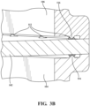
FIG. 3B is a perspective cutaway view of a bead contacting a pattern of solder bumps; -
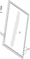
FIG. 4 is a circuit board having first and second predetermined patterns of solder bumps; and -
FIG. 5 is a perspective cutaway view of the electronic device having multiple circuit boards mounted in parallel. - Elements in the figures are illustrated for simplicity and clarity and have not necessarily been rendered according to any sequence. For example, steps that may be performed concurrently or in different order are illustrated in the figures to help to improve understanding of embodiments of the present disclosure.
- While various aspects of the present disclosure are described with reference to an electronic device in an automotive application, the present disclosure is not limited to such embodiments, and additional modifications, applications, and embodiments may be implemented without departing from the present disclosure. In the figures, like reference numbers will be used to illustrate the same components. Those skilled in the art will recognize that the various components set forth herein may be altered without varying from the scope of the present disclosure.
-
FIG. 1 is a simplified representation, in a perspective view, of anelectronic device 100 having at least onecircuit board 102 clamped between afirst enclosure member 104 and asecond enclosure member 106. In practice, thecircuit board 102 is sandwiched and fastened between the first andsecond enclosure members fasteners 108, such as screws or clips, strategically placed predetermined distances from each other around a perimeter of thedevice 100. -
FIG. 2 is a cutaway view of theelectronic device 100. Theenclosure members predetermined distance 110 around thecircuit board 102 for clearance to accommodate electronic components on the circuit board and in the housing. Additionally, at least oneenclosure member circuit board 102 from other components within the enclosure and shields the electronic device from electronic devices external to the enclosure. This is accomplished through a consistent contact to ground between the solder balls on thecircuit board 102 and at least one of the first andsecond enclosure members circuit board 102. At least one of the first andsecond enclosure members -
FIG. 3A is a close-up view of theelectronic device 100 showing theenclosure members circuit board 102 in contact with each other along one or more contact zones. The contact zones are areas where thecircuit board 102 and theenclosures FIG. 3A , the contact zones are an entire perimeter of each of thecircuit board 102, thefirst enclosure member 104 and thesecond enclosure member 106. - The contact zone of the
circuit board 102 has a predetermined pattern ofsolder bumps 112, such as one row around its perimeter on each surface as shown inFIG. 4 . Referring toFIG. 3B , asurface 114 of eachenclosure member circuit board 102 has abead 116 that protrudes from the enclosure member. Thebead 116 has a predetermined pattern that substantially matches the predetermined pattern of solder bumps so that when thecircuit board 102 is clamped between theenclosure members solder bumps 112. Instead of contact being consistently made only at the fastener locations, contact occurs at contact zones along thebead 116 on eachenclosure member 104, 06 where it contacts thesolder bumps 112 on thecircuit board 102. In the example shown inFIGS. 3A and3B , the contact is made all along the perimeter (or any other location where thebead 116,solder bump 112 connection may be introduced) to sustain sufficient electrical contact. - The
bead 116 may be found on both enclosures (as shown) but it is necessary for thebead 116 on at least one of theenclosures enclosure 104 and/or 106 and a pattern of solder bumps 112 on thecircuit board 102 to ensure electrical contact. In one or more embodiments, thebead 116 is triangular. Acontinuous bead 116 around the perimeter of theenclosures circuit board 102. However, thebead 116 may have a different profile shape to accommodate design specifications and limitations. - As discussed above, the
bead 116 may be around a perimeter of theenclosures circuit board 102 to facilitate a ground connection that protects theelectronic device 100 from external interference and from causing excessive emissions. However, thebead 116 on the surface of at least one of theenclosure members circuit board 102 may also be implemented in other areas and have points of contact between at least one of theenclosure members circuit board 102 other than just the perimeter. For example, the bead may contact at least a second pattern of solder bumps on an interior of thecircuit board 102 that, for example, surrounds a particular component on the board, to isolate and protect the component form internal interference. - Contact of the
bead 116 with the pattern of solder bumps 112 on thecircuit board 102 provides consistent electrical contact. Gaps in a ground connection could adversely affect EMC. Theperimeter bead 116 provides consistent electrical contact even in areas where circuit board deformation might typically occur, such as the areas between fasteners. When fasteners are over-clamped during assembly, or when the circuit board is otherwise warped or deformed, gaps in ground contact may occur. Gaps may also occur when one or more of the fasteners comes loose, for example from vibrations of the electronic, such as road vibrations of a vehicle. The continuous contact of thebead 116 with the solder bumps 112 addresses these problems. Thebead 116 on the enclosure members contacting the pattern of solder bumps 112 on thecircuit board 102 provides a more consistent contact to ground than the fasteners alone. -
FIG. 5 shows one or more embodiments 500 of the inventive subject matter having first 504, second 506 and at least a third 518 enclosure members. First 502 and second 520 circuit boards are enclosed by theenclosure members second circuit boards FIG. 4 . Referring again toFIG. 5 , Thethird enclosure member 518 is positioned between the first andsecond circuit boards enclosure members bead 516 that has a predetermined pattern substantially matching the pattern of solder bumps 512 for contacting the pattern of solder bumps 512 on either, or both, of thecircuit boards - The
third enclosure member 518 has a perimeter bead having a predetermined pattern, for example, along each edge so that it contacts the pattern of solder bumps 512 on at least one of thecircuit boards third enclosure member 518 also has a planar surface section that divides the enclosure to provide structural support for multiple circuit boards in parallel. The planar surface may also function as a heat sink for hot components on any one of the circuit boards. Within the enclosure, there is spacing 510 between each of thecircuit boards bead 516 on each of its surfaces to contact solder bumps on each of thecircuit boards second circuit boards spaces 510 above and below thecircuit boards bead 516 on the first, second and at least athird enclosure members second circuit boards - In the foregoing specification, the present disclosure has been described with reference to specific exemplary embodiments. The specification and figures are illustrative, rather than restrictive, and modifications are intended to be included within the scope of the present disclosure. Accordingly, the scope of the present disclosure should be determined by the claims and their legal equivalents rather than by merely the examples described.
- For example, the components and/or elements recited in any apparatus claims may be assembled or otherwise operationally configured in a variety of permutations and are accordingly not limited to the specific configuration recited in the claims.
- Benefits, other advantages, and solutions to problems have been described above regarding specific embodiments. However, any benefit, advantage, solution to problem or any element that may cause any particular benefit, advantage, or solution to occur or to become more pronounced are not to be construed as critical, required, or essential features or components of any or all the claims.
- The terms "comprise", "comprises", "comprising", "having", "including", "includes" or any variation thereof, are intended to reference a non-exclusive inclusion, such that a process, method, article, composition, or apparatus that comprises a list of elements does not include only those elements recited but may also include other elements not expressly listed or inherent to such process, method, article, composition, or apparatus. Other combinations and/or modifications of the above-described structures, arrangements, applications, proportions, elements, materials, or components used in the practice of the present disclosure, in addition to those not specifically recited, may be varied, or otherwise particularly adapted to specific environments, manufacturing specifications, design parameters or other operating requirements without departing from the general principles of the same.
Claims (15)
- An electronic device comprising:at least one circuit board having a predetermined pattern of solder bumps facilitating a ground connection; anda first enclosure member and a second enclosure member, wherein the at least one circuit board is sandwiched between the first and second enclosure members, each of the first and second enclosure members has a surface facing the circuit board and the surface facing the circuit board has a bead extending therefrom, the bead contacts the predetermined pattern of solder bumps to complete the ground connection.
- The electronic device of claim 1, wherein the bead is a triangular shape.
- The electronic device of claim 1 or 2, whereineither the predetermined pattern of solder bumps is a row of solder bumps along a perimeter of at least one surface of the circuit board, orthe predetermined pattern of solder bumps is a pattern of solder bumps around a component on the circuit board.
- The electronic device of any of claims 1 to 3, wherein the predetermined pattern of solder bumps further comprises:a first predetermined pattern of solder bumps around a perimeter of the circuit board;at least a second predetermined pattern of solder bumps around at least one component on an interior of the circuit board; andwherein the bead extends from the surface facing the circuit board in a manner that contacts the first and the at least a second predetermined patterns of solder bumps.
- The electronic device of any of claims 1 to 4, further comprising:at least a third enclosure member positioned between the first and second enclosure members, the at least a third enclosure member has a first surface with a bead extending therefrom, a second surface with a bead extending therefrom, and a planar surface parallel to the first and second enclosure members;a first circuit board has a predetermined pattern of solder bumps facilitating a ground connection, a perimeter edge of the first circuit board is sandwiched between the first enclosure member and the third enclosure member;at least a second circuit board has a predetermined pattern of solder bumps facilitating a ground connection, a perimeter edge of the second circuit board is sandwiched between the second enclosure member and the third enclosure member;the bead on any one of the first enclosure member or the third enclosure member contacts the predetermined pattern of solder bumps on the first circuit board to complete the ground connection and the bead on any one of the second enclosure member or the third enclosure member contacts the pattern of solder bumps on the at least a second circuit board to complete the ground connection;the first enclosure member and the third enclosure member are parallel to the first circuit board and spaced a distance to create a space above the first circuit board; andthe third enclosure member and the second enclosure member are parallel to the second circuit board and spaced a distance to create a space below the second circuit board.
- An electronic device comprising:at least one circuit board having a predetermined pattern of solder bumps facilitating a ground connection;first and second enclosure members, each having a surface facing the at least one circuit board sandwiching the circuit board between the surfaces; anda bead protruding from the surface of the enclosure member facing the at least one circuit board, the bead contacts the predetermined pattern of solder bumps.
- The electronic device of claim 6, wherein the predetermined pattern of solder bumps is around a perimeter of the circuit board and the bead extends along a perimeter of the first and second enclosure members shielding the at least one circuit board from external interference.
- The electronic device of claim 6, wherein the predetermined pattern of solder bumps is around at least one component on the circuit board, and the bead extends from the surface of the first and second enclosure members in a pattern that matches the predetermined pattern of solder bumps thereby shielding the at least one component of the circuit board from internal interference.
- The electronic device of any of claims 6 to 8, wherein the predetermined pattern of solder bumps further comprises:a first predetermined pattern of solder bumps around a perimeter of the circuit board;the bead extends along a perimeter of the surface of the first and second enclosures contacting the first predetermined pattern of solder bumps shielding the at least one circuit board from external interference;at least a second predetermined pattern of solder bumps around at least one component of the circuit board; andthe bead also extends from the surface of the first and second enclosures in a pattern that matches the at least a second predetermined pattern of solder bumps shielding the at least one component of the circuit board from internal interference.
- The electronic device of any of claims 6 to 9, further comprising:at least a third enclosure member positioned between the first and second enclosure members;the at least one circuit board is sandwiched between the first enclosure member and the third enclosure member;a bead protruding from a first surface of the at least a third enclosure member;a bead protruding from a second surface of the at least a third enclosure member;at least a second circuit board sandwiched between the second enclosure member and the third enclosure member, the second circuit board has a predetermined pattern of solder bumps facilitating a ground connection; andat least one of the beads contacts the predetermined pattern of solder bumps on the at least a second circuit board to complete the ground connection.
- An electronic device comprising:a plurality of circuit boards, each circuit board has a first predetermined pattern of solder bumps facilitating a ground connection for the electronic device;a plurality of enclosure members that enclose the plurality of circuit boards and create space between each enclosure member and each circuit board; anda first bead protruding from a perimeter edge of each enclosure member, the bead contacts the first predetermined pattern of solder bumps on the circuit board to complete a ground connection.
- The electronic device of claim 11, wherein the bead is triangular.
- The electronic device of claim 11 or 12 wherein the predetermined pattern of solder bumps further comprises at least one row of solder bumps around a perimeter of each circuit board in the plurality of circuit boards.
- The electronic device of any of claims 11 to 13, wherein the predetermined pattern of solder bumps further comprises a row of solder bumps around a component on one circuit board of the plurality of circuit boards.
- The electronic device of any of claims 1 to 14, wherein the predetermined pattern of solder bumps further comprises:a first predetermined pattern of solder bumps around a perimeter of one circuit board of the plurality of circuit boards, wherein the bead extends from a surface of at least one enclosure member facing the first predetermined pattern of solder bumps around a perimeter of the circuit board and contacts the first predetermined pattern of solder bumps to complete the ground connection;a second predetermined pattern of solder bumps around at least one component on an interior of one of the circuit boards in the plurality of circuit boards; anda second bead extending from at least one of the plurality of enclosure members, the second bead has a pattern that matches the second predetermined pattern of solder bumps, the second bead contacts the second predetermined pattern of solder bumps to isolate the at least one component.
Applications Claiming Priority (1)
| Application Number | Priority Date | Filing Date | Title |
|---|---|---|---|
| US17/463,832 US11641718B2 (en) | 2021-09-01 | 2021-09-01 | Electromagnetic compatibility contact between metal castings and printed circuit boards |
Publications (1)
| Publication Number | Publication Date |
|---|---|
| EP4145962A1 true EP4145962A1 (en) | 2023-03-08 |
Family
ID=83362395
Family Applications (1)
| Application Number | Title | Priority Date | Filing Date |
|---|---|---|---|
| EP22193367.4A Pending EP4145962A1 (en) | 2021-09-01 | 2022-09-01 | Electromagnetic compatibility contact between metal castings and printed circuit boards |
Country Status (3)
| Country | Link |
|---|---|
| US (3) | US11641718B2 (en) |
| EP (1) | EP4145962A1 (en) |
| CN (1) | CN115734595A (en) |
Families Citing this family (1)
| Publication number | Priority date | Publication date | Assignee | Title |
|---|---|---|---|---|
| WO2025211998A1 (en) * | 2024-04-04 | 2025-10-09 | Magna Electronics Sweden Ab | Enhanced pcb and pcb housing |
Citations (6)
| Publication number | Priority date | Publication date | Assignee | Title |
|---|---|---|---|---|
| US4658334A (en) * | 1986-03-19 | 1987-04-14 | Rca Corporation | RF signal shielding enclosure of electronic systems |
| EP0727932A2 (en) * | 1994-11-28 | 1996-08-21 | Kabushiki Kaisha Toshiba | Electromagnetic shielded casing |
| DE102008003787A1 (en) * | 2008-01-10 | 2009-07-16 | Robert Bosch Gmbh | Printed circuit board arrangement for controller, particularly engine controller for internal combustion engine, has housing with two electrically conductive housing pieces |
| EP2230892A1 (en) * | 2009-03-18 | 2010-09-22 | Alcatel Lucent | Electro-magnetic sealing with solder bump array gasket on printed circuit board |
| EP3240387A1 (en) * | 2016-04-05 | 2017-11-01 | Harman International Industries, Incorporated | Electromagnetic shield for an electronic device |
| EP3316666A1 (en) * | 2016-10-25 | 2018-05-02 | Robert Bosch GmbH | Method for manufacturing an electronic element and electronic element |
Family Cites Families (6)
| Publication number | Priority date | Publication date | Assignee | Title |
|---|---|---|---|---|
| US3665136A (en) * | 1971-03-16 | 1972-05-23 | Martin Gaber | Reed switch construction |
| KR101068550B1 (en) * | 2010-02-03 | 2011-09-30 | 조인셋 주식회사 | Easy soldering shield case for electromagnetic shielding |
| JP5149320B2 (en) * | 2010-03-17 | 2013-02-20 | 株式会社ソニー・コンピュータエンタテインメント | Electronics |
| US9462732B2 (en) * | 2013-03-13 | 2016-10-04 | Laird Technologies, Inc. | Electromagnetic interference shielding (EMI) apparatus including a frame with drawn latching features |
| KR102612900B1 (en) * | 2016-09-30 | 2023-12-13 | 삼성전자주식회사 | contact element and contact structure for electronic apparatus |
| DE112018008084T5 (en) * | 2018-10-18 | 2021-07-08 | Mitsubishi Electric Corporation | Circuit board housing |
-
2021
- 2021-09-01 US US17/463,832 patent/US11641718B2/en active Active
-
2022
- 2022-08-24 CN CN202211017863.0A patent/CN115734595A/en active Pending
- 2022-09-01 EP EP22193367.4A patent/EP4145962A1/en active Pending
-
2023
- 2023-03-31 US US18/193,823 patent/US12150252B2/en active Active
- 2023-03-31 US US18/193,803 patent/US12150251B2/en active Active
Patent Citations (6)
| Publication number | Priority date | Publication date | Assignee | Title |
|---|---|---|---|---|
| US4658334A (en) * | 1986-03-19 | 1987-04-14 | Rca Corporation | RF signal shielding enclosure of electronic systems |
| EP0727932A2 (en) * | 1994-11-28 | 1996-08-21 | Kabushiki Kaisha Toshiba | Electromagnetic shielded casing |
| DE102008003787A1 (en) * | 2008-01-10 | 2009-07-16 | Robert Bosch Gmbh | Printed circuit board arrangement for controller, particularly engine controller for internal combustion engine, has housing with two electrically conductive housing pieces |
| EP2230892A1 (en) * | 2009-03-18 | 2010-09-22 | Alcatel Lucent | Electro-magnetic sealing with solder bump array gasket on printed circuit board |
| EP3240387A1 (en) * | 2016-04-05 | 2017-11-01 | Harman International Industries, Incorporated | Electromagnetic shield for an electronic device |
| EP3316666A1 (en) * | 2016-10-25 | 2018-05-02 | Robert Bosch GmbH | Method for manufacturing an electronic element and electronic element |
Also Published As
| Publication number | Publication date |
|---|---|
| US12150251B2 (en) | 2024-11-19 |
| US20230240021A1 (en) | 2023-07-27 |
| US12150252B2 (en) | 2024-11-19 |
| US20230067621A1 (en) | 2023-03-02 |
| US11641718B2 (en) | 2023-05-02 |
| US20230247773A1 (en) | 2023-08-03 |
| CN115734595A (en) | 2023-03-03 |
Similar Documents
| Publication | Publication Date | Title |
|---|---|---|
| JP7467696B2 (en) | Electronic Board Mounting System | |
| US5691504A (en) | Multilayer computer chassis having integral circuit board mounting and grounding structure | |
| JP3270028B2 (en) | Electromagnetic shield plate, electromagnetic shield structure, and entertainment device | |
| US5847938A (en) | Press-fit shields for electronic assemblies, and methods for assembling the same | |
| US6796485B2 (en) | Solder-bearing electromagnetic shield | |
| US7609530B2 (en) | Conductive elastomeric shielding device and method of forming same | |
| US20130050962A1 (en) | Electromagnetic interference shield | |
| CN104869796A (en) | Fastening structure for shield can | |
| US7280368B2 (en) | EMI shielding techniques using multiple EMI shields which share the same circuit board holes | |
| EP0726700B1 (en) | A shielding device | |
| US12150252B2 (en) | Electromagnetic compatibility contact between metal castings and printed circuit boards | |
| CN107396621B (en) | Electromagnetic shield for electronic device | |
| NL1036864C2 (en) | Circuit board having isolation cover and assembling method thereof. | |
| US3723943A (en) | Methods of securing flat integrated circuits to printed wiring boards and a support device therefor | |
| US20020051344A1 (en) | Covering device for ceramic modules | |
| JP3028956B1 (en) | Environmentally friendly FG structure | |
| US6992894B1 (en) | Method and apparatus for EMI shielding | |
| US6661670B1 (en) | Apparatus, assembly and system for enhancing EMI shielding | |
| CN222395984U (en) | EMC shielding cover and electronic equipment | |
| EP4622019A1 (en) | Rf connector and communication device comprising same | |
| US20050133252A1 (en) | Printed circuit board noise suppression device and method of manufacturing | |
| JPH08288683A (en) | Shield structure of package type electronic component unit | |
| KR101015246B1 (en) | Shield plate mounting structure for electronic products | |
| WO2002005612A2 (en) | Method and apparatus for emi shielding of electrical components | |
| CN120282398A (en) | Electronic module |
Legal Events
| Date | Code | Title | Description |
|---|---|---|---|
| PUAI | Public reference made under article 153(3) epc to a published international application that has entered the european phase |
Free format text: ORIGINAL CODE: 0009012 |
|
| STAA | Information on the status of an ep patent application or granted ep patent |
Free format text: STATUS: THE APPLICATION HAS BEEN PUBLISHED |
|
| AK | Designated contracting states |
Kind code of ref document: A1 Designated state(s): AL AT BE BG CH CY CZ DE DK EE ES FI FR GB GR HR HU IE IS IT LI LT LU LV MC MK MT NL NO PL PT RO RS SE SI SK SM TR |
|
| STAA | Information on the status of an ep patent application or granted ep patent |
Free format text: STATUS: REQUEST FOR EXAMINATION WAS MADE |
|
| 17P | Request for examination filed |
Effective date: 20230508 |
|
| RBV | Designated contracting states (corrected) |
Designated state(s): AL AT BE BG CH CY CZ DE DK EE ES FI FR GB GR HR HU IE IS IT LI LT LU LV MC MK MT NL NO PL PT RO RS SE SI SK SM TR |
|
| STAA | Information on the status of an ep patent application or granted ep patent |
Free format text: STATUS: EXAMINATION IS IN PROGRESS |
|
| 17Q | First examination report despatched |
Effective date: 20250429 |