EP4145694A1 - Matrix power conversion device and control method thereof - Google Patents
Matrix power conversion device and control method thereof Download PDFInfo
- Publication number
- EP4145694A1 EP4145694A1 EP22155842.2A EP22155842A EP4145694A1 EP 4145694 A1 EP4145694 A1 EP 4145694A1 EP 22155842 A EP22155842 A EP 22155842A EP 4145694 A1 EP4145694 A1 EP 4145694A1
- Authority
- EP
- European Patent Office
- Prior art keywords
- voltage
- phase
- max
- carrier wave
- output
- Prior art date
- Legal status (The legal status is an assumption and is not a legal conclusion. Google has not performed a legal analysis and makes no representation as to the accuracy of the status listed.)
- Pending
Links
- 238000006243 chemical reaction Methods 0.000 title claims abstract description 52
- 239000011159 matrix material Substances 0.000 title claims abstract description 50
- 238000000034 method Methods 0.000 title claims description 15
- 230000002457 bidirectional effect Effects 0.000 claims abstract description 117
- 238000002347 injection Methods 0.000 description 8
- 239000007924 injection Substances 0.000 description 8
- 239000003990 capacitor Substances 0.000 description 5
- 230000015572 biosynthetic process Effects 0.000 description 4
- 238000003786 synthesis reaction Methods 0.000 description 4
- 230000003247 decreasing effect Effects 0.000 description 3
- 238000010586 diagram Methods 0.000 description 3
- 230000001052 transient effect Effects 0.000 description 1
Images




Classifications
-
- H—ELECTRICITY
- H02—GENERATION; CONVERSION OR DISTRIBUTION OF ELECTRIC POWER
- H02P—CONTROL OR REGULATION OF ELECTRIC MOTORS, ELECTRIC GENERATORS OR DYNAMO-ELECTRIC CONVERTERS; CONTROLLING TRANSFORMERS, REACTORS OR CHOKE COILS
- H02P27/00—Arrangements or methods for the control of AC motors characterised by the kind of supply voltage
- H02P27/04—Arrangements or methods for the control of AC motors characterised by the kind of supply voltage using variable-frequency supply voltage, e.g. inverter or converter supply voltage
- H02P27/16—Arrangements or methods for the control of AC motors characterised by the kind of supply voltage using variable-frequency supply voltage, e.g. inverter or converter supply voltage using AC to AC converters without intermediate conversion to DC
-
- H—ELECTRICITY
- H02—GENERATION; CONVERSION OR DISTRIBUTION OF ELECTRIC POWER
- H02M—APPARATUS FOR CONVERSION BETWEEN AC AND AC, BETWEEN AC AND DC, OR BETWEEN DC AND DC, AND FOR USE WITH MAINS OR SIMILAR POWER SUPPLY SYSTEMS; CONVERSION OF DC OR AC INPUT POWER INTO SURGE OUTPUT POWER; CONTROL OR REGULATION THEREOF
- H02M1/00—Details of apparatus for conversion
- H02M1/0048—Circuits or arrangements for reducing losses
-
- H—ELECTRICITY
- H02—GENERATION; CONVERSION OR DISTRIBUTION OF ELECTRIC POWER
- H02M—APPARATUS FOR CONVERSION BETWEEN AC AND AC, BETWEEN AC AND DC, OR BETWEEN DC AND DC, AND FOR USE WITH MAINS OR SIMILAR POWER SUPPLY SYSTEMS; CONVERSION OF DC OR AC INPUT POWER INTO SURGE OUTPUT POWER; CONTROL OR REGULATION THEREOF
- H02M1/00—Details of apparatus for conversion
- H02M1/42—Circuits or arrangements for compensating for or adjusting power factor in converters or inverters
- H02M1/4208—Arrangements for improving power factor of AC input
- H02M1/4216—Arrangements for improving power factor of AC input operating from a three-phase input voltage
-
- H—ELECTRICITY
- H02—GENERATION; CONVERSION OR DISTRIBUTION OF ELECTRIC POWER
- H02M—APPARATUS FOR CONVERSION BETWEEN AC AND AC, BETWEEN AC AND DC, OR BETWEEN DC AND DC, AND FOR USE WITH MAINS OR SIMILAR POWER SUPPLY SYSTEMS; CONVERSION OF DC OR AC INPUT POWER INTO SURGE OUTPUT POWER; CONTROL OR REGULATION THEREOF
- H02M5/00—Conversion of AC power input into AC power output, e.g. for change of voltage, for change of frequency, for change of number of phases
- H02M5/02—Conversion of AC power input into AC power output, e.g. for change of voltage, for change of frequency, for change of number of phases without intermediate conversion into DC
- H02M5/04—Conversion of AC power input into AC power output, e.g. for change of voltage, for change of frequency, for change of number of phases without intermediate conversion into DC by static converters
- H02M5/22—Conversion of AC power input into AC power output, e.g. for change of voltage, for change of frequency, for change of number of phases without intermediate conversion into DC by static converters using discharge tubes with control electrode or semiconductor devices with control electrode
- H02M5/275—Conversion of AC power input into AC power output, e.g. for change of voltage, for change of frequency, for change of number of phases without intermediate conversion into DC by static converters using discharge tubes with control electrode or semiconductor devices with control electrode using devices of a triode or transistor type requiring continuous application of a control signal
- H02M5/293—Conversion of AC power input into AC power output, e.g. for change of voltage, for change of frequency, for change of number of phases without intermediate conversion into DC by static converters using discharge tubes with control electrode or semiconductor devices with control electrode using devices of a triode or transistor type requiring continuous application of a control signal using semiconductor devices only
- H02M5/2932—Conversion of AC power input into AC power output, e.g. for change of voltage, for change of frequency, for change of number of phases without intermediate conversion into DC by static converters using discharge tubes with control electrode or semiconductor devices with control electrode using devices of a triode or transistor type requiring continuous application of a control signal using semiconductor devices only with automatic control of output voltage, current or power
Definitions
- the present disclosure relates to a power conversion device and a control method thereof, and more particularly to a matrix power conversion device and a control method thereof.
- the drive should be connected to an AC power source.
- the AC power is converted into a DC-link capacitor voltage through a diode rectifier or an active-front-end, and then the drive converts the DC power to the AC motor side.
- the energy conversion process is in order of AC, DC and AC.
- a DC capacitor needs to be provided as a relay buffer for energy, which makes the overall volume larger and causes the efficiency to decrease.
- a matrix power conversion device Through the operation of a plurality of bidirectional switches in the matrix power conversion device, an AC power at the input side is directly converted into an AC power at the output side. There is no need to dispose an additional DC capacitor as relay buffer. Consequently, by the matrix power conversion device and the control thereof of the present disclosure, the matrix power conversion device with smaller volume, better efficiency and longer lifespan is realized.
- the present disclosure utilizes carrier wave to control the bidirectional switches of the matrix power conversion device, so as to realize the synthesis of output voltage and output current.
- a matrix power conversion device coupled between a three-phase input power and a motor.
- the matrix power conversion device includes a plurality of three-phase switching modules and a controller.
- the plurality of three-phase switching modules switches the three-phase input power to generate a three-phase output power.
- Each three-phase switching module includes a plurality of bidirectional switches, each bidirectional switch of each three-phase switching module is connected to a corresponding input phase voltage of the three-phase input power, and each three-phase switching module outputs a corresponding output phase voltage of the three-phase output power.
- the controller acquires all input phase voltages of the three-phase input power, and determines a maximum voltage, an intermediate voltage and a minimum voltage among all the input phase voltages to acquire a waveform of a control carrier wave in a switching cycle.
- the controller acquires output expected values corresponding to all output phase voltages of the three-phase output power.
- the controller compares the waveform of the control carrier wave with all the output expected values respectively for acquiring a turning-on time of each of the plurality of bidirectional switches. According to the turning-on time of each of the plurality of bidirectional switches, the controller controls the matrix power conversion device to switch the three-phase input power so as to change the three-phase output power for driving the motor.
- the matrix power conversion device includes a plurality of three-phase switching modules and a controller.
- the plurality of three-phase switching modules switches the three-phase input power to generate a three-phase output power.
- Each three-phase switching module includes a plurality of bidirectional switches, each bidirectional switch in each three-phase switching module is connected to a corresponding input phase voltage of the three-phase input power, and each three-phase switching module outputs a corresponding output phase voltage of the three-phase output power.
- the control method includes: acquiring all input phase voltages of the three-phase input power; determining a maximum voltage, an intermediate voltage and a minimum voltage among all the input phase voltages to acquire a waveform of a control carrier wave in a switching cycle; acquiring output expected values corresponding to all output phase voltages of the three-phase output power respectively; comparing the waveform of the control carrier wave with all the output expected values respectively for acquiring a turning-on time of each of the plurality of bidirectional switches; and switching the three-phase input power to change the three-phase output power for driving a motor according to the turning-on time of each bidirectional switch.
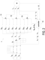
- FIG. 2 is a schematic circuit diagram illustrating a matrix power conversion device according to an embodiment of the present disclosure.
- the matrix power conversion device 1 is coupled between a three-phase input power and a motor M.
- the matrix power conversion device 1 includes a plurality of three-phase switching modules 11, 12 and 13 and a controller 14.
- the plurality of three-phase switching modules 11, 12, and 13 switches the three-phase input power to generate a three-phase output power.
- Each three-phase switching module includes a plurality of bidirectional switches (S au , S bu , S cu , S av , S bv , S cv , S aw , S bw , S cw ), and each bidirectional switch in each three-phase switching module (11, 12, 13) is connected to the corresponding input phase voltage of the three-phase input power. Further, each three-phase switching module outputs the corresponding output phase voltage of the three-phase output power.
- the three-phase switching module 11 includes bidirectional switches S au , S bu and S cu connected to input phase voltages v a , v b and v c of the three-phase input power respectively;
- the three-phase switching module 12 includes bidirectional switches S av , S bv and S cv connected to input phase voltages v a , v b and v c of the three-phase input power respectively;
- the three-phase switching module 13 includes bidirectional switches S aw , S bw and S cw connected to input phase voltages v a , v b and v c of the three-phase input power respectively.
- the three-phase switching modules 11, 12 and 13 output the output phase voltages v u , v v and v w of the three-phase output power respectively.
- the number of the three-phase switching modules, the input phase voltages, and the output phase voltages are all equal to three, but the present disclosure is not limited thereto.
- FIG. 3 is a schematic flow chart illustrating a control method of the matrix power conversion device according to an embodiment of the present disclosure.
- the controller 14 of FIG. 2 is utilized to perform the control method of FIG. 3 , so as to implement the control for the matrix power conversion device and the three-phase switching modules 11, 12 and 13 thereof. As shown in FIG. 2 and FIG.
- the controller 14 acquires all input phase voltages v a , v b and v c (Step S1), and determines a maximum voltage, an intermediate voltage and a minimum voltage among the input phase voltages v a , v b and v c to acquire a waveform of a control carrier wave in a switching cycle (Step S2). Then, the controller 14 acquires output expected values corresponding to the output phase voltages v u , v v and v w respectively (Step S3).
- the controller 14 compares the waveform of the control carrier wave with the output expected values corresponding to the output phase voltage v u , v v and v w respectively for acquiring the turning-on time of each of the bidirectional switches S au , S bu , S cu , S av , S bv , S cv , S aw , S bw and S cw in the switching cycle (Step S4).
- the controller 14 outputs control signals for controlling all the bidirectional switch S au to S cw , thereby controlling the matrix power conversion device 1 to switch the three-phase input power to adjust the three-phase output power for driving the motor M (Step S5).
- the controller 14 further receives an angular speed ⁇ and an angle ⁇ of the motor M operating to obtain the operating status of the motor M.
- the matrix power conversion device 1 With smaller volume, better efficiency and longer lifespan is implemented.
- FIG. 4 shows a specific structure of the bidirectional switches S au to S cw .
- each bidirectional switch includes two switches connected in series.
- the bidirectional switch S au includes switches S au1 and S au2 connected in series
- the bidirectional switch S bu includes switches S bu1 and S bu2 connected in series
- the bidirectional switch S cw includes switches S cw1 and S cw2 connected in series.
- the controller 14 outputs the control signals of the switches S au1 to S cw2 in order to implement the control for the switches S au1 to S cw2 .
- the control signals of the two switches in any bidirectional switch are the same, and are only slightly out of phase with respect to each other during transient switching so as to avoid input short circuit or output open circuit.
- control carrier wave to control the bidirectional switches S au to S cw of the matrix power conversion device 1 for implementing the synthesis of the output voltage and input current. It should be noted that the control described as follows is performed by the controller 14 of FIG. 2 .
- D au to D cw are duty ratios of the control signals of the bidirectional switches S au to S cw respectively, namely D au to D cw are ratios of the turning-on time of the bidirectional switches S au to S cw in one switching cycle.
- the output phase voltages v u , v v and v w can be synthesized from the input phase voltages v a , v b and v c
- the input phase currents i a , i b and i c can be synthesized from the output phase currents i u , i v and i w . It is noted that in each of the three-phase switching modules 11, 12 and 13 at any time, there must be one bidirectional switch in an on state and the other bidirectional switches in an off state.
- the output phase voltages v u , v v and v w of the matrix power conversion device 1 are synthesized from the input phase voltages v a , v b and v c through the switching combination of the bidirectional switches.
- the output phase voltages v u , v v and v w of the matrix power conversion device 1 are synthesized from the input phase voltages v a , v b and v c through the switching combination of the bidirectional switches.
- only one output phase is analyzed as follows since the control and operation principles for each output phase are similar.
- FIG. 5 shows the equivalent circuit of a three-phase switching module in one switching cycle.
- v k represents any of the output phase voltages, where k can be u, v or w.
- all the input phase voltages v a , v b and v c in FIG. 2 are compared with each other, and E i_max , E i_mid and E i_min in FIG. 5 respectively represents the maximum voltage, the intermediate voltage and the minimum voltage among the input phase voltages v a , v b and v c .
- the bidirectional switches S k_max , S k_mid and S k_min are connected to the input phase voltages corresponding to the maximum voltage E i_max , the intermediate voltage E i_mid and the minimum voltage E i_min respectively.
- the output phase voltage v k is determined by the duty ratios of the bidirectional switches S k_max , S k_mid and S k_min in one switching cycle, as shown in equation (4):
- v k D k _ max ⁇ E i _ max + D k _ mid ⁇ E i _ mid + D k _ min ⁇ E i _ min
- the turning-on time of the bidirectional switches S k_max , S k_mid and S k_min are corresponding to the maximum duty ratio D k_max , the intermediate duty ratio D k_mid and the minimum duty ratio D k_min respectively.
- the sum of the maximum duty ratio D k_max , the intermediate duty ratio D k_mid and the minimum duty ratio D k_min equals 1.
- the required output phase voltages can be synthesized.
- the appropriate duty ratios of all the bidirectional switches are acquired based on the control carrier wave, and the required output phase voltages can be synthesized accordingly, which is described specifically as follows.
- FIG. 6 is a schematic oscillogram showing the input phase voltages and the base voltage command.
- the waveforms of the input phase voltages v a , v b and v c are all sinusoidal and are depicted by dashed lines.
- each of the input phase voltages v a , v b and v c of the three-phase input power is captured according to a preset phase, and the input phase voltage with the largest absolute voltage value is regarded as the base voltage command E base .
- E base the base voltage command
- the waveform of the base voltage command E base is depicted by solid line.
- the preset phase is for example but not limited to 30 degrees or ⁇ /6 radians.
- the positive interval is defined as the time interval in which the base voltage command E base is positive, and the base voltage command E base is equal to the maximum voltage E i_max in the positive interval.
- the negative interval is defined as the time interval in which the base voltage command E base is negative, and the base voltage command E base is equal to the minimum voltage E i_min in the negative interval.
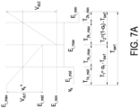
- FIG. 7A is a schematic oscillogram showing the control carrier wave, the output expected value and the output phase voltage in one switching cycle during the base voltage command E base being in the positive interval.
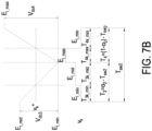
- FIG. 7B is a schematic oscillogram showing the control carrier wave, the output expected value and the output phase voltage in one switching cycle during the base voltage command E base being in the negative interval.
- v k can be any output phase voltage
- v k ⁇ is the output expected value corresponding to the output phase voltage v k .
- the average value of the output phase voltage v k in one switching cycle is equal to the corresponding output expected value v k ⁇ .
- the waveform of the control carrier wave includes a first linear carrier wave and a second linear carrier wave.
- the slope of the first linear carrier wave is negative.
- there is a first voltage difference V dc1 between the maximum voltage E i_max and the intermediate voltage E i_mid there is a first voltage difference V dc1 between the maximum voltage E i_max and the intermediate voltage E i_mid , and the first voltage difference V dc1 is the voltage variation of the first linear carrier wave.
- the bidirectional switch S k_mid when the first linear carrier wave is greater than the output expected value v k ⁇ , the bidirectional switch S k_mid is in the on state so that the output phase voltage v k is equal to the intermediate voltage E i_mid , and the turning-on time of the bidirectional switch S k_mid is T 1k_mid .
- the bidirectional switch S k_max When the first linear carrier wave is less than the output expected value v k ⁇ , the bidirectional switch S k_max is in the on state so that the output phase voltage v k is equal to the maximum voltage E i_max , and the turning-on time of the bidirectional switch S k_max is T 1k_max .
- the slope of the second linear carrier wave is positive.
- the bidirectional switch S k_max is in the on state so that the output phase voltage v k is equal to the maximum voltage E i_max , and the turning-on time of the bidirectional switch S k_max is T 2k_max .
- the bidirectional switch S k_min When the second linear carrier wave is greater than the output expected value v k ⁇ , the bidirectional switch S k_min is in the on state so that the output phase voltage v k is equal to the minimum voltage E i_min , and the turning-on time of the bidirectional switch S k_min is T 2k_min .
- the controller 14 retrieves the time of the first linear carrier wave being greater than the output expected value v k ⁇ to acquire the corresponding intermediate duty ratio D k_mid .
- the turning-on time of the bidirectional switch S k_mid corresponding to the intermediate voltage E i_mid is corresponding to the intermediate duty ratio D k_mid .
- the controller 14 retrieves a first time of the first linear carrier wave being less than the output expected value v k ⁇ and acquires a second time of the second linear carrier wave being less than the output expected value v k ⁇ .
- the controller 14 adds the first time and the second time up to acquire the corresponding maximum duty ratio D k_max .
- the turning-on time of the bidirectional switch S k_max corresponding to the maximum voltage E i_max is corresponding to the maximum duty ratio D k_max .
- the controller 14 retrieves the time of the second linear carrier wave being greater than the output expected value v k ⁇ to acquire the corresponding minimum duty ratio D k_min .
- the turning-on time of the bidirectional switch S k_min corresponding to the minimum voltage E i_min is corresponding to the minimum duty ratio D k_min .
- the waveform of the control carrier wave includes a first linear carrier wave and a second linear carrier wave.
- the slope of the first linear carrier wave is negative.
- there is a third voltage difference V dc3 between the intermediate voltage E i_mid and the minimum voltage E i_min is the third voltage difference V dc3 is the voltage variation of the first linear carrier wave.
- the bidirectional switch S k_min is in the on state so that the output phase voltage v k is equal to the minimum voltage E i_min , and the turning-on time of the bidirectional switch S k_min is T 3k_min .
- the bidirectional switch S k_mid When the first linear carrier wave is less than the output expected value v k ⁇ , the bidirectional switch S k_mid is in the on state so that the output phase voltage v k is equal to the intermediate voltage E i_mid , and the turning-on time of the bidirectional switch S k_mid is T 3k_mid .
- the slope of the second linear carrier wave is positive.
- there is a fourth voltage difference V dc4 between the maximum voltage E i_max and the minimum voltage E i_min and the fourth voltage difference V dc4 is the voltage variation of the second linear carrier wave.
- the bidirectional switch S k_max is in the on state so that the output phase voltage v k is equal to the maximum voltage E i_max , and the turning-on time of the bidirectional switch S k_max is T 4k_max .
- the bidirectional switch S k_min When the second linear carrier wave is greater than the output expected value v k ⁇ , the bidirectional switch S k_min is in the on state so that the output phase voltage v k is equal to the minimum voltage E i_min , and the turning-on time of the bidirectional switch S k_min is T 4k_min .
- the controller 14 retrieves a first time of the first linear carrier wave being greater than the output expected value v k ⁇ and acquires a second time of the second linear carrier wave being greater than the output expected value v k ⁇ . Further, the controller 14 adds the first time and the second time up to acquire the corresponding minimum duty ratio D k_min .
- the turning-on time of the bidirectional switch S k_min corresponding to the minimum voltage E i_min is corresponding to the minimum duty ratio D k_min .
- the controller 14 retrieves the time of the first linear carrier wave being less than the output expected value v k ⁇ to acquire the corresponding intermediate duty ratio D k_mid .
- the turning-on time of the bidirectional switch S k_mid corresponding to the intermediate voltage E i_mid is corresponding to the intermediate duty ratio D k_mid
- the controller 14 retrieves the time of the second linear carrier wave being less than the output expected value v k ⁇ to acquire the corresponding maximum duty ratio D k_max .
- the turning-on time of the bidirectional switch S k_max corresponding to the maximum voltage E i_max is corresponding to the maximum duty ratio D k_max .
- the required output phase voltage v k can be synthesized.
- the synthesis of the input current can be realized by adjusting the duration of the first and second linear carrier waves, which is described specifically as follows.
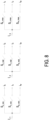
- FIG. 8 shows the relations between the input phase currents and the output phase currents and the equivalent circuit of the bidirectional switches.
- the input phase currents i a , i b and i c in FIG. 2 the input phase currents respectively corresponding to the minimum voltage E i_min , the intermediate voltage E i_mid and the maximum voltage E i_max are the input phase currents I i_1 , I i_2 and I i_3 in FIG. 8 respectively.
- the input phase currents I i_1 , I i_2 and I i_3 are the input phase currents I i_1 , I i_2 and I i_3 in FIG. 8 respectively.
- I i _ 1 ⁇ 1 ⁇ ⁇ 1 V dc 2 v u * ⁇ i u + v v * ⁇ i v + v w * ⁇ i w
- I i _ 2 ⁇ ⁇ 1 V dc 1 v u * ⁇ i u + v v * ⁇ i v + v w * ⁇ i w
- I i _ 3 v u * ⁇ i u + v v * ⁇ i v + v w * ⁇ i w ⁇ 1 V dc 1 + 1 ⁇ ⁇ 1 V dc 2
- ⁇ 1 ⁇ V dc 1 E i _ mid V dc 2 ⁇ V dc 1 E i _ mid + E i _ max V dc 2
- I i _ 1 v u * ⁇ i u + v v * ⁇ i v + v w * ⁇ i w ⁇ 2 V dc 3 + 1 ⁇ ⁇ 2 V dc 4
- I i _ 2 ⁇ ⁇ 2 V dc 3 v u * ⁇ i u + v v * ⁇ i v + v w * ⁇ i w
- I i _ 3 ⁇ 1 ⁇ ⁇ 2 V dc 4 v u * ⁇ i u + v v * ⁇ i v + v w * ⁇ i w
- ⁇ 2 ⁇ V dc 3 E i _ mid V dc 4 ⁇ V dc 3 E i _ mid + E i _ max V dc 4
- a zero sequence voltage can be injected into the output expected values of three phases, which is described specifically as follows.
- FIG. 9A schematically shows the waveforms of the control carrier wave, the three-phase output expected values v u ⁇ , v v ⁇ and v w ⁇ and the output phase voltages v u , v v and v w .
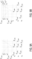
- FIG. 9B shows the relations between the three-phase output expected values v u ⁇ , v v ⁇ and v w ⁇ after zero sequence injection and the control carrier wave.
- the bidirectional switch S u_max is maintained in the on state in one switching cycle T sw1 . Therefore, the switching times of the bidirectional switch are decreased, and the switching loss is reduced.
- the controller 14 calculates the average voltage values of all the output phase voltage v u , v v and v w , and selects a maximum value of all the average voltage values as a reference base voltage. Further, the controller 14 calculates a voltage difference between the maximum voltage E i_max and the reference base voltage as a shift voltage (i.e., the zero sequence voltage).
- the shift voltage is added to each of the output phase voltages v u , v v and v w respectively, so as to obtain the output expected values v u ⁇ , v v ⁇ and v w ⁇ .
- FIG. 10A schematically shows the waveforms of the control carrier wave, the three-phase output expected values v u ⁇ , v v ⁇ and v w ⁇ and the output phase voltages v u , v v and v w .
- FIG. 10B shows the relations between the three-phase output expected values v u ⁇ , v v ⁇ and v w ⁇ after zero sequence injection and the control carrier wave. As shown in FIG.
- the bidirectional switch S w_max is maintained in the on state in one switching cycle T sw2 . Therefore, the switching times of the bidirectional switch are decreased, and the switching loss is reduced.
- the controller 14 calculates the average voltage values of all the output phase voltage v u , v v and v w , and selects a minimum value of all the average voltage values as a reference base voltage. Further, the controller 14 calculates a voltage difference between the minimum voltage E i_min and the reference base voltage as a shift voltage (i.e., the zero sequence voltage).
- the shift voltage is subtracted from each of the output phase voltages v u , v v and v w respectively, so as to obtain the output expected values v u ⁇ , v v ⁇ and v w ⁇ .
- the first and second linear carrier waves of the control carrier wave have unequal cycle variation and voltage variation, but the present disclosure is not limited thereto.
- the first and second linear carrier waves of the control carrier wave have the same cycle variation and voltage variation.
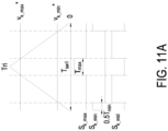
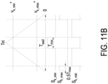
- FIG. 11A and FIG. 11B schematically show the waveforms of the control carrier wave and the control signals of the bidirectional switches in the case of the first and second linear carrier waves having the same cycle variation and voltage variation.
- the control carrier wave is a symmetrical triangular wave
- Tri is the amplitude of the control carrier wave
- T max is the total turning-on time of the bidirectional switch S k_max in one switching cycle
- T min is the total turning-on time of the bidirectional switch S k_min in one switching cycle.
- the turning-on time T max and T min of the bidirectional switches S k_max and S k_min corresponding to any output phase can be acquired according to equation (5).
- the voltage commands v k_max ⁇ and v k_min ⁇ are compared with the control carrier wave.
- the bidirectional switch S k_max is controlled to be turned on.
- the bidirectional switch S k_max is controlled to be turned off.
- the bidirectional switch S k_min When the voltage command v k_min ⁇ is greater than the control carrier wave, the bidirectional switch S k_min is controlled to be turned on. When the voltage command v k_min ⁇ is less than the control carrier wave, the bidirectional switch S k_min is controlled to be turned off.
- the turning-on time T max and T min of the bidirectional switches S k_max and S k_min corresponding to any output phase can be acquired according to equation (7).
- the voltage commands v k_max ⁇ and v k_min ⁇ are compared with the control carrier wave.
- the bidirectional switch S k_min is controlled to be turned on.
- the bidirectional switch S k_min is controlled to be turned off.
- the bidirectional switch S k_max When the voltage command v k_max ⁇ is greater than the control carrier wave, the bidirectional switch S k_max is controlled to be turned on. When the voltage command v k_max ⁇ is less than the control carrier wave, the bidirectional switch S k_max is controlled to be turned off.
- the control signals of the bidirectional switches S k_max and S k_min is generated.
- the bidirectional switch S k_mid is turned on when the bidirectional switches S k_max and S k_min are both turned off.
- the present disclosure provides a matrix power conversion device and a control method thereof.
- the matrix power conversion device Through the operation of the plurality of bidirectional switches in the matrix power conversion device, the AC power at the input side is directly converted into the AC power at the output side. There is no need to dispose an additional DC capacitor as relay buffer. Consequently, by the matrix power conversion device and the control thereof of the present disclosure, the matrix power conversion device with smaller volume, better efficiency and longer lifespan is realized.
- the present disclosure utilizes carrier wave to control the bidirectional switches of the matrix power conversion device, so as to realize the synthesis of output voltage and output current.
- the zero sequence voltage is injected into the output expected values of three phases, thereby decreasing the switching times of the bidirectional switch and reducing the switching loss.
- the first and second linear carrier waves of the control carrier wave have equal or unequal cycle variation and voltage variation.
- the control carrier wave is a symmetrical triangular wave for ease of implementing and controlling.
Landscapes
- Engineering & Computer Science (AREA)
- Power Engineering (AREA)
- Ac-Ac Conversion (AREA)
Abstract
Description
- The present disclosure relates to a power conversion device and a control method thereof, and more particularly to a matrix power conversion device and a control method thereof.
- In various industrial applications of motor drive, the drive should be connected to an AC power source. As shown in
FIG. 1 , the AC power is converted into a DC-link capacitor voltage through a diode rectifier or an active-front-end, and then the drive converts the DC power to the AC motor side. In this structure, the energy conversion process is in order of AC, DC and AC. However, in this model, a DC capacitor needs to be provided as a relay buffer for energy, which makes the overall volume larger and causes the efficiency to decrease. - Therefore, there is a need of providing a matrix power conversion device and a control method thereof to obviate the drawbacks encountered from the prior arts.
- It is an objective of the present disclosure to provide a matrix power conversion device and a control method thereof. Through the operation of a plurality of bidirectional switches in the matrix power conversion device, an AC power at the input side is directly converted into an AC power at the output side. There is no need to dispose an additional DC capacitor as relay buffer. Consequently, by the matrix power conversion device and the control thereof of the present disclosure, the matrix power conversion device with smaller volume, better efficiency and longer lifespan is realized. In addition, the present disclosure utilizes carrier wave to control the bidirectional switches of the matrix power conversion device, so as to realize the synthesis of output voltage and output current.
- In accordance with an aspect of the present disclosure, there is provided a matrix power conversion device coupled between a three-phase input power and a motor. The matrix power conversion device includes a plurality of three-phase switching modules and a controller. The plurality of three-phase switching modules switches the three-phase input power to generate a three-phase output power. Each three-phase switching module includes a plurality of bidirectional switches, each bidirectional switch of each three-phase switching module is connected to a corresponding input phase voltage of the three-phase input power, and each three-phase switching module outputs a corresponding output phase voltage of the three-phase output power. The controller acquires all input phase voltages of the three-phase input power, and determines a maximum voltage, an intermediate voltage and a minimum voltage among all the input phase voltages to acquire a waveform of a control carrier wave in a switching cycle. The controller acquires output expected values corresponding to all output phase voltages of the three-phase output power. The controller compares the waveform of the control carrier wave with all the output expected values respectively for acquiring a turning-on time of each of the plurality of bidirectional switches. According to the turning-on time of each of the plurality of bidirectional switches, the controller controls the matrix power conversion device to switch the three-phase input power so as to change the three-phase output power for driving the motor.
- In accordance with another aspect of the present disclosure, there is provided a control method for a matrix power conversion device. The matrix power conversion device includes a plurality of three-phase switching modules and a controller. The plurality of three-phase switching modules switches the three-phase input power to generate a three-phase output power. Each three-phase switching module includes a plurality of bidirectional switches, each bidirectional switch in each three-phase switching module is connected to a corresponding input phase voltage of the three-phase input power, and each three-phase switching module outputs a corresponding output phase voltage of the three-phase output power. The control method includes: acquiring all input phase voltages of the three-phase input power; determining a maximum voltage, an intermediate voltage and a minimum voltage among all the input phase voltages to acquire a waveform of a control carrier wave in a switching cycle; acquiring output expected values corresponding to all output phase voltages of the three-phase output power respectively; comparing the waveform of the control carrier wave with all the output expected values respectively for acquiring a turning-on time of each of the plurality of bidirectional switches; and switching the three-phase input power to change the three-phase output power for driving a motor according to the turning-on time of each bidirectional switch.
-
-
FIG. 1 a schematic diagram showing the application of the conventional motor and motor drive; -
FIG. 2 is a schematic circuit diagram illustrating a matrix power conversion device according to an embodiment of the present disclosure; -
FIG. 3 is a schematic flow chart illustrating a control method of the matrix power conversion device according to an embodiment of the present disclosure; -
FIG. 4 schematically shows a specific structure of the bidirectional switches ofFIG. 2 ; -
FIG. 5 shows the equivalent circuit of a three-phase switching module in one switching cycle; -
FIG. 6 is a schematic oscillogram showing the input phase voltages and the base voltage command ofFIG. 2 ; -
FIG. 7A is a schematic oscillogram showing the control carrier wave, the output expected value and the output phase voltage in one switching cycle during the base voltage command ofFIG. 6 being in the positive interval; -
FIG. 7B is a schematic oscillogram showing the control carrier wave, the output expected value and the output phase voltage in one switching cycle during the base voltage command ofFIG. 6 being in the negative interval; -
FIG. 8 shows the relations between the input phase currents and the output phase currents and the equivalent circuit of the bidirectional switches; -
FIG. 9A schematically shows the waveforms of the control carrier wave, the three-phase output expected values and the output phase voltages in one switching cycle during the base voltage command being in the positive interval; -
FIG. 9B shows the waveforms of the three-phase output expected values ofFIG. 9A after zero sequence injection; -
FIG. 10A schematically shows the waveforms of the control carrier wave, the three-phase output expected values and the output phase voltages in one switching cycle during the base voltage command being in the negative interval; -
FIG. 10B shows the waveforms of the three-phase output expected values ofFIG. 10A after zero sequence injection; -
FIG. 11A andFIG. 11B schematically show the waveforms of the control carrier wave and the control signals of the bidirectional switches in the case of the first and second linear carrier waves having the same cycle variation and voltage variation. - The present disclosure will now be described more specifically with reference to the following embodiments. It is to be noted that the following descriptions of preferred embodiments of this disclosure are presented herein for purpose of illustration and description only. It is not intended to be exhaustive or to be limited to the precise form disclosed.
-
FIG. 2 is a schematic circuit diagram illustrating a matrix power conversion device according to an embodiment of the present disclosure. As shown inFIG. 2 , the matrixpower conversion device 1 is coupled between a three-phase input power and a motor M. The matrixpower conversion device 1 includes a plurality of three-phase switching modules controller 14. The plurality of three-phase switching modules phase switching module 11 includes bidirectional switches Sau, Sbu and Scu connected to input phase voltages va, vb and vc of the three-phase input power respectively; the three-phase switching module 12 includes bidirectional switches Sav, Sbv and Scv connected to input phase voltages va, vb and vc of the three-phase input power respectively; and the three-phase switching module 13 includes bidirectional switches Saw, Sbw and Scw connected to input phase voltages va, vb and vc of the three-phase input power respectively. Moreover, the three-phase switching modules - Please refer to
FIG. 2 andFIG. 3. FIG. 3 is a schematic flow chart illustrating a control method of the matrix power conversion device according to an embodiment of the present disclosure. In the present disclosure, thecontroller 14 ofFIG. 2 is utilized to perform the control method ofFIG. 3 , so as to implement the control for the matrix power conversion device and the three-phase switching modules FIG. 2 andFIG. 3 , firstly, thecontroller 14 acquires all input phase voltages va, vb and vc(Step S1), and determines a maximum voltage, an intermediate voltage and a minimum voltage among the input phase voltages va, vb and vc to acquire a waveform of a control carrier wave in a switching cycle (Step S2). Then, thecontroller 14 acquires output expected values corresponding to the output phase voltages vu, vv and vw respectively (Step S3). Afterwards, thecontroller 14 compares the waveform of the control carrier wave with the output expected values corresponding to the output phase voltage vu, vv and vw respectively for acquiring the turning-on time of each of the bidirectional switches Sau, Sbu, Scu, Sav, Sbv, Scv, Saw, Sbw and Scw in the switching cycle (Step S4). Finally, according to the turning-on time of each bidirectional switch Sau to Scw, thecontroller 14 outputs control signals for controlling all the bidirectional switch Sau to Scw, thereby controlling the matrixpower conversion device 1 to switch the three-phase input power to adjust the three-phase output power for driving the motor M (Step S5). In an embodiment, thecontroller 14 further receives an angular speed ω and an angle θ of the motor M operating to obtain the operating status of the motor M. - Therefore, through the plurality of bidirectional switches Sau to Scw of the matrix
power conversion device 1, the AC power at the input side can be directly converted into the AC power at the output side. There is no need to dispose an additional DC capacitor as relay buffer. Consequently, by the matrixpower conversion device 1 and the control method thereof of the present disclosure, the matrixpower conversion device 1 with smaller volume, better efficiency and longer lifespan is implemented. - In addition,
FIG. 4 shows a specific structure of the bidirectional switches Sau to Scw. As shown inFIG. 4 , each bidirectional switch includes two switches connected in series. In particular, the bidirectional switch Sau includes switches Sau1 and Sau2 connected in series, the bidirectional switch Sbu includes switches Sbu1 and Sbu2 connected in series, and so on, the bidirectional switch Scw includes switches Scw1 and Scw2 connected in series. Correspondingly, thecontroller 14 outputs the control signals of the switches Sau1 to Scw2 in order to implement the control for the switches Sau1 to Scw2. Generally, the control signals of the two switches in any bidirectional switch are the same, and are only slightly out of phase with respect to each other during transient switching so as to avoid input short circuit or output open circuit. - The following would describe how to utilize a control carrier wave to control the bidirectional switches Sau to Scw of the matrix
power conversion device 1 for implementing the synthesis of the output voltage and input current. It should be noted that the control described as follows is performed by thecontroller 14 ofFIG. 2 . - As shown in
FIG. 2 , each phase at the output side is connected to the three-phase input power through the three bidirectional switches of the corresponding three-phase switching module. Therefore, the average output phase voltages vu, vv and vw in a switching cycle are defined as:
where Dau to Dcw are duty ratios of the control signals of the bidirectional switches Sau to Scw respectively, namely Dau to Dcw are ratios of the turning-on time of the bidirectional switches Sau to Scw in one switching cycle. The input phase currents ia, ib and ic of the three-phase input power are defined as:
where iu, iv and iw are the output phase currents of the three-phase output power. - Accordingly, the output phase voltages vu, vv and vw can be synthesized from the input phase voltages va, vb and vc, and the input phase currents ia, ib and ic can be synthesized from the output phase currents iu, iv and iw. It is noted that in each of the three-
phase switching modules phase switching modules 
- In equation (3), when Sau equals 1, it means that the bidirectional switch Sau is in the on state; and when Sau equals 0, it means that the bidirectional switch Sau is in the off state. Similarly, Sbu to Scw in equation (3) reflects the on or off state of the other bidirectional switches Sbu to Scw.
- It can be seen from the above descriptions that the output phase voltages vu, vv and vw of the matrix
power conversion device 1 are synthesized from the input phase voltages va, vb and vc through the switching combination of the bidirectional switches. In order to facilitate the description and understanding, only one output phase is analyzed as follows since the control and operation principles for each output phase are similar. -
FIG. 5 shows the equivalent circuit of a three-phase switching module in one switching cycle. InFIG. 5 , vk represents any of the output phase voltages, where k can be u, v or w. Furthermore, all the input phase voltages va, vb and vc inFIG. 2 are compared with each other, and Ei_max, E i_mid and Ei_min inFIG. 5 respectively represents the maximum voltage, the intermediate voltage and the minimum voltage among the input phase voltages va, vb and vc. The bidirectional switches Sk_max, Sk_mid and Sk_min are connected to the input phase voltages corresponding to the maximum voltage Ei_max, the intermediate voltage Ei_mid and the minimum voltage Ei_min respectively. As mentioned above, in each three-phase switching module at any time, there is only one bidirectional switch in the on state. Therefore, the output phase voltage vk is determined by the duty ratios of the bidirectional switches Sk_max, Sk_mid and Sk_min in one switching cycle, as shown in equation (4):
- The turning-on time of the bidirectional switches Sk_max, Sk_mid and Sk_min are corresponding to the maximum duty ratio Dk_max, the intermediate duty ratio Dk_mid and the minimum duty ratio Dk_min respectively. The sum of the maximum duty ratio Dk_max, the intermediate duty ratio Dk_mid and the minimum duty ratio Dk_min equals 1.
- Accordingly, once the appropriate duty ratios are determined, the required output phase voltages can be synthesized. In the present disclosure, the appropriate duty ratios of all the bidirectional switches are acquired based on the control carrier wave, and the required output phase voltages can be synthesized accordingly, which is described specifically as follows.
- In order to achieve the best voltage utilization, firstly, it is necessary to determine the magnitude relations among the input phase voltages va, vb and vc in each time interval.
FIG. 6 is a schematic oscillogram showing the input phase voltages and the base voltage command. InFIG. 6 , the waveforms of the input phase voltages va, vb and vc are all sinusoidal and are depicted by dashed lines. In addition, each of the input phase voltages va, vb and vc of the three-phase input power is captured according to a preset phase, and the input phase voltage with the largest absolute voltage value is regarded as the base voltage command Ebase. InFIG. 6 , the waveform of the base voltage command Ebase is depicted by solid line. The preset phase is for example but not limited to 30 degrees or π/6 radians. Through the output phase voltages synthesized based on the voltage command Ebase, the best voltage utilization is achieved. As shown inFIG. 6 , the positive interval is defined as the time interval in which the base voltage command Ebase is positive, and the base voltage command Ebase is equal to the maximum voltage Ei_max in the positive interval. On the contrary, the negative interval is defined as the time interval in which the base voltage command Ebase is negative, and the base voltage command Ebase is equal to the minimum voltage Ei_min in the negative interval. -
FIG. 7A is a schematic oscillogram showing the control carrier wave, the output expected value and the output phase voltage in one switching cycle during the base voltage command Ebase being in the positive interval.FIG. 7B is a schematic oscillogram showing the control carrier wave, the output expected value and the output phase voltage in one switching cycle during the base voltage command Ebase being in the negative interval. InFIG. 7A andFIG. 7B , vk can be any output phase voltage, vk ∗ is the output expected value corresponding to the output phase voltage vk. In the present disclosure, through controlling the bidirectional switches by the control carrier wave, the average value of the output phase voltage vk in one switching cycle is equal to the corresponding output expected value vk ∗. - As shown in
FIG. 7A , when the base voltage command Ebase is in the positive interval (i.e., Ebase = Ei_max), the waveform of the control carrier wave includes a first linear carrier wave and a second linear carrier wave. The cycle variation of the first linear carrier wave is the first switching interval T1 of the switching cycle Tsw1, and the first switching interval T1 is equal to the product of a time ratio value α1 and the switching cycle Tsw1 (i.e., T1=α1·Tsw1). The cycle variation of the second linear carrier wave is the second switching interval T2 of the switching cycle Tsw1, and the second switching interval T2 is equal to the difference between the switching cycle Tsw1 and the first switching interval T1 (i.e., T2=(1-α1)·Tsw1). - The slope of the first linear carrier wave is negative. During the first switching interval T1, there is a first voltage difference Vdc1 between the maximum voltage Ei_max and the intermediate voltage Ei_mid, and the first voltage difference Vdc1 is the voltage variation of the first linear carrier wave. In addition, during the first switching interval T1, when the first linear carrier wave is greater than the output expected value vk ∗, the bidirectional switch Sk_mid is in the on state so that the output phase voltage vk is equal to the intermediate voltage Ei_mid, and the turning-on time of the bidirectional switch Sk_mid is T1k_mid. When the first linear carrier wave is less than the output expected value vk ∗, the bidirectional switch Sk_max is in the on state so that the output phase voltage vk is equal to the maximum voltage Ei_max, and the turning-on time of the bidirectional switch Sk_max is T1k_max.
- The slope of the second linear carrier wave is positive. During the second switching interval T2, there is a second voltage difference Vdc2 between the maximum voltage Ei_max and the minimum voltage Ei_min, and the second voltage difference Vdc2 is the voltage variation of the second linear carrier wave. In addition, during the second switching interval T2, when the second linear carrier wave is less than the output expected value vk ∗, the bidirectional switch Sk_max is in the on state so that the output phase voltage vk is equal to the maximum voltage Ei_max, and the turning-on time of the bidirectional switch Sk_max is T2k_max. When the second linear carrier wave is greater than the output expected value vk ∗, the bidirectional switch Sk_min is in the on state so that the output phase voltage vk is equal to the minimum voltage Ei_min, and the turning-on time of the bidirectional switch Sk_min is T2k_min.
- According to the waveforms shown in
FIG. 7A , the turning-on time of each interval is derived as:
- In addition, according to the turning-on time of each bidirectional switches in one switching cycle Tsw1, the average output phase voltage vk in one switching cycle Tsw1 is calculated as:

- Through substituting the equation (5) into the equation (6), it is derived that vk=vk ∗, which proves that the average value of the output phase voltage vk in one switching cycle Tsw1 is equal to the output expected value vk ∗.
- Therefore, when the base voltage command Ebase is in the positive interval (i.e., Ebase = Ei_max), the
controller 14 retrieves the time of the first linear carrier wave being greater than the output expected value vk ∗ to acquire the corresponding intermediate duty ratio Dk_mid. The turning-on time of the bidirectional switch Sk_mid corresponding to the intermediate voltage Ei_mid is corresponding to the intermediate duty ratio Dk_mid. In addition, thecontroller 14 retrieves a first time of the first linear carrier wave being less than the output expected value vk ∗ and acquires a second time of the second linear carrier wave being less than the output expected value vk ∗. Further, thecontroller 14 adds the first time and the second time up to acquire the corresponding maximum duty ratio Dk_max. The turning-on time of the bidirectional switch Sk_max corresponding to the maximum voltage Ei_max is corresponding to the maximum duty ratio Dk_max. Furthermore, thecontroller 14 retrieves the time of the second linear carrier wave being greater than the output expected value vk ∗ to acquire the corresponding minimum duty ratio Dk_min. The turning-on time of the bidirectional switch Sk_min corresponding to the minimum voltage Ei_min is corresponding to the minimum duty ratio Dk_min. - On the other hand, as shown in
FIG. 7B , when the base voltage command Ebase is in the negative interval (i.e., Ebase = Ei_min), the waveform of the control carrier wave includes a first linear carrier wave and a second linear carrier wave. The cycle variation of the first linear carrier wave is the first switching interval T3 of the switching cycle Tsw2, and the first switching interval T3 is equal to the product of a time ratio value α2 and the switching cycle Tsw2 (i.e., T3=α2·Tsw2). The cycle variation of the second linear carrier wave is the second switching interval T4 of the switching cycle Tsw2, and the second switching interval T4 is equal to the difference between the switching cycle Tsw2 and the first switching interval T3 (i.e., T4=(1-α2)·Tsw2). - The slope of the first linear carrier wave is negative. During the first switching interval T3, there is a third voltage difference Vdc3 between the intermediate voltage Ei_mid and the minimum voltage Ei_min, and the third voltage difference Vdc3 is the voltage variation of the first linear carrier wave. In addition, during the first switching interval T3, when the first linear carrier wave is greater than the output expected value vk ∗, the bidirectional switch Sk_min is in the on state so that the output phase voltage vk is equal to the minimum voltage Ei_min, and the turning-on time of the bidirectional switch Sk_min is T3k_min. When the first linear carrier wave is less than the output expected value vk ∗, the bidirectional switch Sk_mid is in the on state so that the output phase voltage vk is equal to the intermediate voltage Ei_mid, and the turning-on time of the bidirectional switch Sk_mid is T3k_mid.
- The slope of the second linear carrier wave is positive. During the second switching interval T4, there is a fourth voltage difference Vdc4 between the maximum voltage Ei_max and the minimum voltage Ei_min, and the fourth voltage difference Vdc4 is the voltage variation of the second linear carrier wave. In addition, during the second switching interval T4, when the second linear carrier wave is less than the output expected value vk ∗, the bidirectional switch Sk_max is in the on state so that the output phase voltage vk is equal to the maximum voltage Ei_max, and the turning-on time of the bidirectional switch Sk_max is T4k_max. When the second linear carrier wave is greater than the output expected value vk ∗, the bidirectional switch Sk_min is in the on state so that the output phase voltage vk is equal to the minimum voltage Ei_min, and the turning-on time of the bidirectional switch Sk_min is T4k_min.
- According to the waveforms shown in
FIG. 7B , the turning-on time of each interval is derived as:
- In addition, according to the turning-on time of each bidirectional switches in one switching cycle Tsw1, the average output phase voltage vk in one switching cycle Tsw1 is calculated as:

- Through substituting the equation (7) into the equation (8), it is derived that vk=vk ∗, which proves that the average value of the output phase voltage vk in one switching cycle Tsw2 is equal to the output expected value vk ∗.
- Therefore, when the base voltage command Ebase is in the negative interval (i.e., Ebase = Ei_min), the
controller 14 retrieves a first time of the first linear carrier wave being greater than the output expected value vk ∗ and acquires a second time of the second linear carrier wave being greater than the output expected value vk ∗. Further, thecontroller 14 adds the first time and the second time up to acquire the corresponding minimum duty ratio Dk_min. The turning-on time of the bidirectional switch Sk_min corresponding to the minimum voltage Ei_min is corresponding to the minimum duty ratio Dk_min. In addition, thecontroller 14 retrieves the time of the first linear carrier wave being less than the output expected value vk ∗ to acquire the corresponding intermediate duty ratio Dk_mid. The turning-on time of the bidirectional switch Sk_mid corresponding to the intermediate voltage Ei_mid is corresponding to the intermediate duty ratio Dk_mid Furthermore, thecontroller 14 retrieves the time of the second linear carrier wave being less than the output expected value vk ∗ to acquire the corresponding maximum duty ratio Dk_max. The turning-on time of the bidirectional switch Sk_max corresponding to the maximum voltage Ei_max is corresponding to the maximum duty ratio Dk_max. - As known from the above descriptions, through the PWM (pulse width modulation) control signal generated by comparing the control carrier wave with the output expected value vk ∗, the required output phase voltage vk can be synthesized. The synthesis of the input current can be realized by adjusting the duration of the first and second linear carrier waves, which is described specifically as follows.
-
FIG. 8 shows the relations between the input phase currents and the output phase currents and the equivalent circuit of the bidirectional switches. Among the input phase currents ia, ib and ic inFIG. 2 , the input phase currents respectively corresponding to the minimum voltage Ei_min, the intermediate voltage Ei_mid and the maximum voltage Ei_max are the input phase currents Ii_1, Ii_2 and Ii_3 inFIG. 8 respectively. As shown inFIG. 8 , when the base voltage command Ebase is in the positive interval (i.e., Ebase = Ei_max), the input phase currents Ii_1, I i_2 and Ii_3 are expressed as:
- By substituting equation (5) into equation (9), it is derived that:
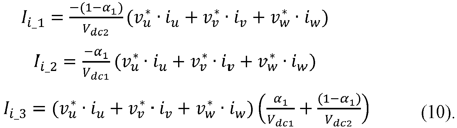
- Equation (10) can be rearranged to be:

- With regard to control the power factor of the input voltage and the input current to equal 1 (i.e., control the input voltage and the input current to be in phase), the equation (11) is substituted into the equation (10), and the input phase current is replaced by the input phase voltage. Therefore, α1 can be acquired as:

- Through substituting α1 of equation (12) into the control carrier wave of
FIG. 7A , the required output voltage and input current with a power factor of 1 can be synthesized when the base voltage command Ebase is in the positive interval (i.e., Ebase = Ei_max). - On the other hand, when the base voltage command Ebase is in the negative interval (i.e., Ebase = Ei_min), the input phase currents Ii_1, I i_2 and Ii_3 are expressed as:

- By substituting equation (7) into equation (13), it is derived that:

- Equation (14) can be rearranged to be:

- With regard to control the power factor of the input voltage and the input current to equal 1 (i.e., control the input voltage and the input current to be in phase), the equation (15) is substituted into the equation (14), and the input phase current is replaced by the input phase voltage. Therefore, α2 can be acquired as:

- Through substituting α2 of equation (16) into the control carrier wave of
FIG. 7B , the required output voltage and input current with a power factor of 1 can be synthesized when the base voltage command Ebase is in the negative interval (i.e., Ebase = Ei_min). - In an embodiment, in order to decrease the times of switching the bidirectional switch for reducing the switching loss, a zero sequence voltage can be injected into the output expected values of three phases, which is described specifically as follows.
- When the base voltage command Ebase is in the positive interval (i.e., Ebase = Ei_max), on the basis of
FIG. 7A ,FIG. 9A schematically shows the waveforms of the control carrier wave, the three-phase output expected values vu ∗, vv ∗ and vw ∗ and the output phase voltages vu, vv and vw. The zero sequence voltage vz is defined as:
- By adding the zero sequence voltage vz to each of the three-phase output expected values vu ∗, vv ∗ and vw ∗ respectively, the three-phase output expected values vu ∗∗, vv ∗∗ and vw ∗∗ after zero sequence injection are acquired as:

-
FIG. 9B shows the relations between the three-phase output expected values vu ∗∗, vv ∗∗ and vw ∗∗ after zero sequence injection and the control carrier wave. As shown inFIG. 9B , among the bidirectional switches Su_max, Su_mid and Su_min corresponding to the output phase voltage vu, the bidirectional switch Su_max is maintained in the on state in one switching cycle Tsw1. Therefore, the switching times of the bidirectional switch are decreased, and the switching loss is reduced. - According to the described principle of zero sequence voltage injection, when the
controller 14 determines that the base voltage command Ebase is in the positive interval (i.e., Ebase = Ei_max), thecontroller 14 calculates the average voltage values of all the output phase voltage vu, vv and vw, and selects a maximum value of all the average voltage values as a reference base voltage. Further, thecontroller 14 calculates a voltage difference between the maximum voltage Ei_max and the reference base voltage as a shift voltage (i.e., the zero sequence voltage). Then, the shift voltage is added to each of the output phase voltages vu, vv and vw respectively, so as to obtain the output expected values vu ∗∗, vv ∗∗ and vw ∗∗. - When the base voltage command Ebase is in the negative interval (i.e., Ebase = Ei_min), on the basis of
FIG. 7B ,FIG. 10A schematically shows the waveforms of the control carrier wave, the three-phase output expected values vu ∗, vv ∗ and vw ∗ and the output phase voltages vu, vv and vw. The zero sequence voltage vz is defined as:
- By adding the zero sequence voltage vz to each of the three-phase output expected values vu ∗, vv ∗ and vw ∗ respectively, the three-phase output expected values vu ∗∗, vv ∗∗ and vw ∗∗ after zero sequence injection are acquired.
FIG. 10B shows the relations between the three-phase output expected values vu ∗∗, vv ∗∗ and vw ∗∗ after zero sequence injection and the control carrier wave. As shown inFIG. 10B , among the bidirectional switches Sw_max, Sw_mid and Sw_min corresponding to the output phase voltage vw, the bidirectional switch Sw_max is maintained in the on state in one switching cycle Tsw2. Therefore, the switching times of the bidirectional switch are decreased, and the switching loss is reduced. - According to the described principle of zero sequence voltage injection, when the
controller 14 determines that the base voltage command Ebase is in the negative interval (i.e., Ebase = Ei_min), thecontroller 14 calculates the average voltage values of all the output phase voltage vu, vv and vw, and selects a minimum value of all the average voltage values as a reference base voltage. Further, thecontroller 14 calculates a voltage difference between the minimum voltage Ei_min and the reference base voltage as a shift voltage (i.e., the zero sequence voltage). Then, the shift voltage is subtracted from each of the output phase voltages vu, vv and vw respectively, so as to obtain the output expected values vu ∗∗, vv ∗∗ and vw ∗∗. - In the above embodiments, the first and second linear carrier waves of the control carrier wave have unequal cycle variation and voltage variation, but the present disclosure is not limited thereto. In another embodiment, for ease of implementing and controlling, the first and second linear carrier waves of the control carrier wave have the same cycle variation and voltage variation.
FIG. 11A andFIG. 11B schematically show the waveforms of the control carrier wave and the control signals of the bidirectional switches in the case of the first and second linear carrier waves having the same cycle variation and voltage variation. InFIG. 11A andFIG. 11B , the control carrier wave is a symmetrical triangular wave, Tri is the amplitude of the control carrier wave, Tmax is the total turning-on time of the bidirectional switch Sk_max in one switching cycle, and Tmin is the total turning-on time of the bidirectional switch Sk_min in one switching cycle. - When the base voltage command Ebase in the positive interval (i.e., Ebase = Ei_max), the turning-on time Tmax and Tmin of the bidirectional switches Sk_max and Sk_min corresponding to any output phase can be acquired according to equation (5). As shown in
FIG. 11A , the voltage commands vk_max ∗ and vk_min ∗ are compared with the control carrier wave. When the voltage command vk_max ∗ is less than the control carrier wave, the bidirectional switch Sk_max is controlled to be turned on. When the voltage command vk_max ∗ is greater than the control carrier wave, the bidirectional switch Sk_max is controlled to be turned off. When the voltage command vk_min ∗ is greater than the control carrier wave, the bidirectional switch Sk_min is controlled to be turned on. When the voltage command vk_min ∗ is less than the control carrier wave, the bidirectional switch Sk_min is controlled to be turned off. It is derived from equation (5) that:
- Through comparing the voltage commands vk_max ∗ and vk_min ∗ with the control carrier wave, the control signals of the bidirectional switches Sk_max and Sk_min is generated. The bidirectional switch Sk_mid is turned on when the bidirectional switches Sk_max and Sk_min are both turned off, which is expressed with XNOR gate as:

- On the other hand, when the base voltage command Ebase in the negative interval (i.e., Ebase = Ei_min), the turning-on time Tmax and Tmin of the bidirectional switches Sk_max and Sk_min corresponding to any output phase can be acquired according to equation (7). As shown in
FIG. 11B , the voltage commands vk_max ∗ and vk_min ∗ are compared with the control carrier wave. When the voltage command vk_min ∗ is less than the control carrier wave, the bidirectional switch Sk_min is controlled to be turned on. When the voltage command vk_min ∗ is greater than the control carrier wave, the bidirectional switch Sk_min is controlled to be turned off. When the voltage command vk_max ∗ is greater than the control carrier wave, the bidirectional switch Sk_max is controlled to be turned on. When the voltage command vk_max ∗ is less than the control carrier wave, the bidirectional switch Sk_max is controlled to be turned off. It is derived from equation (7) that:
- Through comparing the voltage commands vk_max ∗ and vk_min ∗ with the control carrier wave, the control signals of the bidirectional switches Sk_max and Sk_min is generated. The bidirectional switch Sk_mid is turned on when the bidirectional switches Sk_max and Sk_min are both turned off.
- From the above descriptions, the present disclosure provides a matrix power conversion device and a control method thereof. Through the operation of the plurality of bidirectional switches in the matrix power conversion device, the AC power at the input side is directly converted into the AC power at the output side. There is no need to dispose an additional DC capacitor as relay buffer. Consequently, by the matrix power conversion device and the control thereof of the present disclosure, the matrix power conversion device with smaller volume, better efficiency and longer lifespan is realized. In addition, the present disclosure utilizes carrier wave to control the bidirectional switches of the matrix power conversion device, so as to realize the synthesis of output voltage and output current. Moreover, in the present disclosure, the zero sequence voltage is injected into the output expected values of three phases, thereby decreasing the switching times of the bidirectional switch and reducing the switching loss. Further, in the present disclosure, the first and second linear carrier waves of the control carrier wave have equal or unequal cycle variation and voltage variation. For example, the control carrier wave is a symmetrical triangular wave for ease of implementing and controlling.
Claims (14)
- A matrix power conversion device (1), coupled between a three-phase input power and a motor (M), characterized in that the matrix power conversion device (1) comprises:a plurality of three-phase switching modules (11, 12, 13), switching the three-phase input power to generate a three-phase output power, wherein each of the plurality of three-phase switching modules (11) comprises a plurality of bidirectional switches (Sau, Sbu, Scu), each of the plurality of bidirectional switches (Sau, Sbu, Scu) in each of the plurality of three-phase switching modules (11) is connected to a corresponding input phase voltage (va, vb, vc) of the three-phase input power, and each of the plurality of three-phase switching modules (11) outputs a corresponding output phase voltage (vu) of the three-phase output power; anda controller (14), acquiring all input phase voltages (va, vb, vc) of the three-phase input power, and determining a maximum voltage (Ei_max), an intermediate voltage (Ei_mid) and a minimum voltage (Ei_min) among all the input phase voltages (va, vb, vc) to acquire a waveform of a control carrier wave in a switching cycle;wherein the controller (14) acquires output expected values (vk ∗) corresponding to all output phase voltages (vk) of the three-phase output power;wherein the controller (14) compares the waveform of the control carrier wave with all the output expected values (vk ∗) respectively for acquiring a turning-on time of each of the plurality of bidirectional switches (Sk_max, Sk_mid, Sk_min);wherein according to the turning-on time of each of the plurality of bidirectional switches (Sk_max, Sk_mid, Sk_min), the controller (14) controls the matrix power conversion device (1) to switch the three-phase input power so as to change the three-phase output power for driving the motor (M).
- The matrix power conversion device according to claim 1, wherein the waveform of the control carrier wave comprises a first linear carrier wave and a second linear carrier wave, and the controller (14) is further configured to:acquire a time ratio value (α1, α2) according to the maximum voltage (Ei_max), the intermediate voltage (Ei_mid) and the minimum voltage (Ei_min);multiply the switching cycle (Tsw1, Tsw2) by the time ratio value (α1, α2) to acquire a first switching interval (T1, T3) of the switching cycle (Tsw1, Tsw2); andsubtract the first switching interval (T1, T3) from the switching cycle (Tsw1, Tsw2) to acquire a second switching interval (T2, T4) of the switching cycle (Tsw1, Tsw2),wherein the first switching interval (T1, T3) is a cycle variation of the first linear carrier wave, and the second switching interval (T2, T4) is a cycle variation of the second linear carrier wave.
- The matrix power conversion device according to claim 2, wherein the controller (14) is further configured to:select one of the input phase voltages (va, vb, vc) with the largest absolute voltage value to be a base voltage command (Ebase); andidentify whether the base voltage command (Ebase) is positive or negative, and determine a voltage variation of the first linear carrier wave and a voltage variation of the second linear carrier waves according to identifying result.
- The matrix power conversion device according to claim 3, wherein if the controller (14) identifies that the base voltage command (Ebase) is positive, the controller (14) is further configured to:calculate a first voltage difference (Vdc1) between the maximum voltage (Ei_max) and the intermediate voltage (Ei_mid);calculate a second voltage (Vdc2) difference between the maximum voltage (Ei_max) and the minimum voltage (Ei_min); andcalculate the time ratio value (α1) according to the first voltage difference (Vdc1), the second voltage difference (Vdc2), the intermediate voltage (Ei_mid) and the minimum voltage (Ei_max),wherein the first voltage difference (Vdc1) is the voltage variation of the first linear carrier wave, and the second voltage difference (Vdc2) is the voltage variation of the second linear carrier wave; wherein a slope of the first linear carrier wave is negative, and a slope of the second linear carrier wave is positive.
- The matrix power conversion device according to claim 4, wherein the controller (14) is further configured to:retrieve a time of the first linear carrier wave being greater than all the output expected values (vk ∗) respectively, so as to acquire intermediate duty ratios (Dk_mid) corresponding to all the output expected values (vk ∗) respectively;retrieve a first time of the first linear carrier wave being less than all the output expected values (vk ∗) respectively, and retrieve a second time of the second linear carrier wave being less than all the output expected values (vk ∗) respectively;add the first time to the corresponding second time, so as to acquire maximum duty ratios (Dk_max) corresponding to all the output expected values (vk ∗) respectively; andretrieve a time of the second linear carrier wave being greater than all the output expected values (vk ∗) respectively, so as to acquire minimum duty ratios (Dk_min) corresponding to all the output expected values (vk ∗) respectively.
- The matrix power conversion device according to claim 5, wherein a turning-on time (T1k_mid) of the bidirectional switches (Sk_mid) corresponding to the intermediate voltage (Ei_mid) are corresponding to the intermediate duty ratios (Dk_mid) respectively, a turning-on time (Tik_max,T2k_max) of the bidirectional switches (Sk_max) corresponding to the maximum voltage (Ei_max) are corresponding to the maximum duty ratios (Dk_max) respectively, and a turning-on time (T2k_min) of the bidirectional switches (Sk_min) corresponding to the minimum voltage (Ei_min) are corresponding to the minimum duty ratios (Dk_min) respectively.
- The matrix power conversion device according to claim 3, wherein if the controller (14) identifies that the base voltage command (Ebase) is negative, the controller (14) is further configured to:calculate a third voltage difference (Vdc3) between the intermediate voltage (Ei_mid) and the minimum voltage (Ei_min);calculate a fourth voltage difference (Vdc4) between the maximum voltage (Ei_max) and the minimum voltage (Ei_min), andcalculate the time ratio value (α2) according to the third voltage difference (Vdc3), the fourth voltage difference (Vdc4), the intermediate voltage (Ei_mid) and the minimum voltage (Ei_min),wherein the third voltage difference (Vdc3) is the voltage variation of the first linear carrier wave, and the fourth voltage difference (Vdc4) is the voltage variation of the second linear carrier wave; wherein a slope of the first linear carrier wave is negative, and a slope of the second linear carrier wave is positive.
- The matrix power conversion device according to claim 7, wherein the controller (14) is further configured to:retrieve a first time of the first linear carrier wave being greater than all the output expected values (vk ∗) respectively, and retrieve a second time of the second linear carrier wave being greater than all the output expected values respectively;add the first time to the corresponding second time, so as to acquire minimum duty ratios (Dk_min) corresponding to all the output expected values (vk ∗) respectively;retrieve a time of the first linear carrier wave being less than all the output expected values (vk ∗) respectively, so as to acquire intermediate duty ratios (Dk_mid) corresponding to all the output expected values (vk ∗) respectively; andretrieve a time of the second linear carrier wave being less than all the output expected values (vk ∗) respectively, so as to acquire maximum duty ratios (Dk_max) corresponding to all the output expected values (vk ∗) respectively.
- The matrix power conversion device according to claim 8, wherein a turning-on time (T3k_mid) of the bidirectional switches (Sk_mid) corresponding to the intermediate voltage (Ei_mid) are corresponding to the intermediate duty ratios (Dk_mid) respectively, a turning-on time (T4k_max) of the bidirectional switches (Sk_max) corresponding to the maximum voltage (Ei_max) are corresponding to the maximum duty ratios (Dk_max) respectively, and a turning-on time (T3k_min, T4k_min) of the bidirectional switches (Sk_min) corresponding to the minimum voltage (Ei_min) are corresponding to the minimum duty ratios (Dk_min) respectively.
- The matrix power conversion device according to claim 3, wherein if the controller (14) identifies that the base voltage command (Ebase) is positive, the controller (14) is further configured to:calculate average voltage values of all the output phase voltages (vu, vv, vw);select a maximum value of all the average voltage values as a reference base voltage;calculate a voltage difference between the maximum voltage (Ei_max) and the reference base voltage as a shift voltage; andadd the shift voltage to each of the average voltage values, so as to acquire the output expected values (vu ∗∗, vv ∗∗, vw ∗∗).
- The matrix power conversion device according to claim 3, wherein if the controller (14) identifies that the base voltage command (Ebase) is negative, the controller (14) is further configured to:calculate average voltage values of all the output phase voltages (vu, vv, vw);select a minimum value of all the average voltage values as a reference base voltage;calculate a voltage difference between the minimum voltage (Ei_min) and the reference base voltage as a shift voltage; andsubtract the shift voltage from each of the average voltage values, so as to acquire the output expected values (vu ∗∗, vv ∗∗, vw ∗∗).
- The matrix power conversion device according to claim 1, wherein the controller (14) further retrieves each of the input phase voltages (va, vb, vc) of the three-phase input power according to a preset phase, and the preset phase is 30 degrees or π/6 radians.
- The matrix power conversion device according to claim 1, wherein the output expected values (vk ∗) are average voltage values corresponding to the output phase voltages (vk) respectively.
- A control method for a matrix power conversion device (1), wherein the matrix power conversion device (1) comprises a plurality of three-phase switching modules (11, 12, 13) configured to switch the three-phase input power to generate a three-phase output power, each of the plurality of three-phase switching module (11) comprises a plurality of bidirectional switches (Sau, Sbu, Scu), each of the plurality of bidirectional switches (Sau, Sbu, Scu) in each of the plurality of three-phase switching modules (11) is connected to a corresponding input phase voltage (va, vb, vc) of the three-phase input power, each of the plurality of three-phase switching modules (11) outputs a corresponding output phase voltage (vu) of the three-phase output power, characterized in that the control method comprises:acquiring all input phase voltages (va, vb, vc) of the three-phase input power;determining a maximum voltage (Ei_max), an intermediate voltage (Ei_mid) and a minimum voltage (Ei_min) among all the input phase voltages (va, vb, vc) to acquire a waveform of a control carrier wave in a switching cycle;acquiring output expected values (vk ∗) corresponding to all output phase voltages (vk) of the three-phase output power respectively;comparing the waveform of the control carrier wave with all the output expected values (vk ∗) respectively for acquiring a turning-on time of each of the plurality of bidirectional switches (Sk_max, Sk_mid, Sk_min); andswitching the three-phase input power to change the three-phase output power for driving a motor (M) according to the turning-on time of each of the plurality of bidirectional switches (Sk_max, Sk_mid, Sk_min).
Applications Claiming Priority (1)
| Application Number | Priority Date | Filing Date | Title |
|---|---|---|---|
| CN202111022954.9A CN115733420A (en) | 2021-09-01 | 2021-09-01 | Matrix power conversion device and control method thereof |
Publications (1)
| Publication Number | Publication Date |
|---|---|
| EP4145694A1 true EP4145694A1 (en) | 2023-03-08 |
Family
ID=80447001
Family Applications (1)
| Application Number | Title | Priority Date | Filing Date |
|---|---|---|---|
| EP22155842.2A Pending EP4145694A1 (en) | 2021-09-01 | 2022-02-09 | Matrix power conversion device and control method thereof |
Country Status (3)
| Country | Link |
|---|---|
| US (1) | US11870382B2 (en) |
| EP (1) | EP4145694A1 (en) |
| CN (1) | CN115733420A (en) |
Families Citing this family (2)
| Publication number | Priority date | Publication date | Assignee | Title |
|---|---|---|---|---|
| TWI892295B (en) * | 2023-11-08 | 2025-08-01 | 群光電能科技股份有限公司 | Circuit for switching phase power paths |
| WO2025184646A1 (en) * | 2024-03-01 | 2025-09-04 | Borgwarner Inc. | Carrier-based modulation methods for a matrix converter |
Citations (2)
| Publication number | Priority date | Publication date | Assignee | Title |
|---|---|---|---|---|
| GB2458726A (en) * | 2005-04-27 | 2009-10-07 | Yaskawa Denki Seisakusho Kk | Power transforming apparatus and power transforming method |
| US20150130431A1 (en) * | 2013-11-14 | 2015-05-14 | Kabushiki Kaisha Yaskawa Denki | Matrix converter and method for compensating for output voltage error |
Family Cites Families (11)
| Publication number | Priority date | Publication date | Assignee | Title |
|---|---|---|---|---|
| DE19639773A1 (en) | 1996-09-27 | 1998-04-02 | Abb Patent Gmbh | Three-phase matrix converter and method of operation |
| US7848121B2 (en) * | 2007-05-14 | 2010-12-07 | Honeywell International Inc. | Advanced matrix converter and method for operation |
| KR20100009387A (en) * | 2008-07-18 | 2010-01-27 | 명지대학교 산학협력단 | Simulator for wind power generation system |
| CN203670098U (en) | 2011-02-16 | 2014-06-25 | 株式会社安川电机 | Power conversion device for wind power generation, wind power generation device, and wind farm |
| JP5590106B2 (en) * | 2012-12-10 | 2014-09-17 | 株式会社安川電機 | Matrix converter |
| US9531317B2 (en) | 2013-01-25 | 2016-12-27 | Panasonic Intellectual Property Management Co., Ltd. | Power conversion apparatus, power conversion method, and motor system |
| JP2015012729A (en) | 2013-06-28 | 2015-01-19 | 株式会社安川電機 | Matrix converter |
| JP2015096020A (en) | 2013-11-14 | 2015-05-18 | 株式会社安川電機 | Matrix converter and method for compensating output voltage error |
| JP2016046958A (en) | 2014-08-25 | 2016-04-04 | 株式会社安川電機 | Matrix converter, matrix converter control device, and matrix converter control method |
| JP2016067168A (en) | 2014-09-25 | 2016-04-28 | 株式会社安川電機 | Matrix converter, power generation system, and power conversion method |
| CN112448594B (en) * | 2019-08-28 | 2022-05-31 | 台达电子工业股份有限公司 | Indirect matrix converter and rectification module |
-
2021
- 2021-09-01 CN CN202111022954.9A patent/CN115733420A/en active Pending
-
2022
- 2022-01-18 US US17/577,953 patent/US11870382B2/en active Active
- 2022-02-09 EP EP22155842.2A patent/EP4145694A1/en active Pending
Patent Citations (2)
| Publication number | Priority date | Publication date | Assignee | Title |
|---|---|---|---|---|
| GB2458726A (en) * | 2005-04-27 | 2009-10-07 | Yaskawa Denki Seisakusho Kk | Power transforming apparatus and power transforming method |
| US20150130431A1 (en) * | 2013-11-14 | 2015-05-14 | Kabushiki Kaisha Yaskawa Denki | Matrix converter and method for compensating for output voltage error |
Non-Patent Citations (3)
| Title |
|---|
| PIAO CHENGZHU ET AL: "A unified carrier-based modulation method for direct matrix converter", 2015 IEEE INTERNATIONAL CONFERENCE ON ELECTRO/INFORMATION TECHNOLOGY (EIT), IEEE, 21 May 2015 (2015-05-21), pages 122 - 128, XP032790341, DOI: 10.1109/EIT.2015.7293330 * |
| RMILI L ET AL: "A comprehensive analysis of Matrix Converters: Bidirectional switch, direct topology, modeling and control", 2014 IEEE 23RD INTERNATIONAL SYMPOSIUM ON INDUSTRIAL ELECTRONICS (ISIE), IEEE, 1 June 2014 (2014-06-01), pages 313 - 318, XP032623900, DOI: 10.1109/ISIE.2014.6864631 * |
| YOUNG-DOO YOON ET AL: "Carrier-Based Modulation Technique for Matrix Converter", IEEE TRANSACTIONS ON POWER ELECTRONICS, INSTITUTE OF ELECTRICAL AND ELECTRONICS ENGINEERS, USA, vol. 21, no. 6, 1 November 2006 (2006-11-01), pages 1691 - 1703, XP011142859, ISSN: 0885-8993, DOI: 10.1109/TPEL.2006.882935 * |
Also Published As
| Publication number | Publication date |
|---|---|
| US11870382B2 (en) | 2024-01-09 |
| CN115733420A (en) | 2023-03-03 |
| US20230067581A1 (en) | 2023-03-02 |
Similar Documents
| Publication | Publication Date | Title |
|---|---|---|
| EP1814215B1 (en) | Electric power converter and motor driving system | |
| EP2320548B1 (en) | DC bus boost method and system for regenerative brake | |
| US7417393B2 (en) | Load driver capable of suppressing overcurrent | |
| US8724351B2 (en) | Controller for load drive system | |
| US8159851B2 (en) | Matrix converter | |
| US9130481B2 (en) | Power converting appartatus | |
| EP2372894B1 (en) | Direct-current to three-phase alternating-current inverter system | |
| US11870382B2 (en) | Matrix power conversion device and control method thereof | |
| EP2634906A2 (en) | Current-source power converting apparatus | |
| US20150180382A1 (en) | Motor control device | |
| US20150244287A1 (en) | Power conversion apparatus and power conversion method | |
| KR20100084439A (en) | Electric motor driving device for control dc link voltage | |
| JP2014107931A (en) | Method for operating inverter device, and inverter device | |
| CN105471275A (en) | Matrix convertor, power generation system, and method for converting power | |
| US11848600B2 (en) | Power conversion device with control circuit to adjust a common mode voltage of combined output voltages | |
| US9531301B2 (en) | Power conversion device and motor driving device | |
| CN115208273B (en) | Power conversion device and motor control method | |
| US12126276B2 (en) | Power converter and electric apparatus | |
| JP2003079159A (en) | Pulse width modulation type power converter | |
| TWI792530B (en) | Matrix power conversion device and control method thereof | |
| JP2010259181A (en) | Electric motor control device | |
| CN117882287A (en) | Power converter control unit and power conversion device | |
| JP2003209999A (en) | Motor control device | |
| US12202358B2 (en) | Power supply system and moving body | |
| JP2014054037A (en) | One phase-modulation variable speed motor drive |
Legal Events
| Date | Code | Title | Description |
|---|---|---|---|
| PUAI | Public reference made under article 153(3) epc to a published international application that has entered the european phase |
Free format text: ORIGINAL CODE: 0009012 |
|
| STAA | Information on the status of an ep patent application or granted ep patent |
Free format text: STATUS: THE APPLICATION HAS BEEN PUBLISHED |
|
| STAA | Information on the status of an ep patent application or granted ep patent |
Free format text: STATUS: REQUEST FOR EXAMINATION WAS MADE |
|
| AK | Designated contracting states |
Kind code of ref document: A1 Designated state(s): AL AT BE BG CH CY CZ DE DK EE ES FI FR GB GR HR HU IE IS IT LI LT LU LV MC MK MT NL NO PL PT RO RS SE SI SK SM TR |
|
| 17P | Request for examination filed |
Effective date: 20230227 |
|
| RBV | Designated contracting states (corrected) |
Designated state(s): AL AT BE BG CH CY CZ DE DK EE ES FI FR GB GR HR HU IE IS IT LI LT LU LV MC MK MT NL NO PL PT RO RS SE SI SK SM TR |
|
| STAA | Information on the status of an ep patent application or granted ep patent |
Free format text: STATUS: EXAMINATION IS IN PROGRESS |
|
| 17Q | First examination report despatched |
Effective date: 20240223 |