EP4145522A1 - Display panel and display apparatus - Google Patents
Display panel and display apparatus Download PDFInfo
- Publication number
- EP4145522A1 EP4145522A1 EP20911298.6A EP20911298A EP4145522A1 EP 4145522 A1 EP4145522 A1 EP 4145522A1 EP 20911298 A EP20911298 A EP 20911298A EP 4145522 A1 EP4145522 A1 EP 4145522A1
- Authority
- EP
- European Patent Office
- Prior art keywords
- display
- unit
- disposed
- light
- display panel
- Prior art date
- Legal status (The legal status is an assumption and is not a legal conclusion. Google has not performed a legal analysis and makes no representation as to the accuracy of the status listed.)
- Pending
Links
- 125000006850 spacer group Chemical group 0.000 claims description 33
- 239000010409 thin film Substances 0.000 claims description 28
- 229910021417 amorphous silicon Inorganic materials 0.000 claims description 7
- 230000000295 complement effect Effects 0.000 claims description 5
- 229910044991 metal oxide Inorganic materials 0.000 claims description 5
- 150000004706 metal oxides Chemical class 0.000 claims description 5
- 239000004065 semiconductor Substances 0.000 claims description 5
- 239000010410 layer Substances 0.000 description 28
- 239000000463 material Substances 0.000 description 11
- 238000000034 method Methods 0.000 description 8
- 230000002093 peripheral effect Effects 0.000 description 7
- 238000004519 manufacturing process Methods 0.000 description 6
- 230000003287 optical effect Effects 0.000 description 6
- 238000005516 engineering process Methods 0.000 description 5
- 238000000605 extraction Methods 0.000 description 5
- 230000009286 beneficial effect Effects 0.000 description 3
- 239000000758 substrate Substances 0.000 description 3
- 229920001621 AMOLED Polymers 0.000 description 2
- 230000002159 abnormal effect Effects 0.000 description 2
- 230000032683 aging Effects 0.000 description 2
- 238000004458 analytical method Methods 0.000 description 2
- QVGXLLKOCUKJST-UHFFFAOYSA-N atomic oxygen Chemical compound [O] QVGXLLKOCUKJST-UHFFFAOYSA-N 0.000 description 2
- 230000000903 blocking effect Effects 0.000 description 2
- 238000001514 detection method Methods 0.000 description 2
- 230000000694 effects Effects 0.000 description 2
- 239000002346 layers by function Substances 0.000 description 2
- 229910052760 oxygen Inorganic materials 0.000 description 2
- 239000001301 oxygen Substances 0.000 description 2
- XLYOFNOQVPJJNP-UHFFFAOYSA-N water Substances O XLYOFNOQVPJJNP-UHFFFAOYSA-N 0.000 description 2
- 241001270131 Agaricus moelleri Species 0.000 description 1
- 230000003213 activating effect Effects 0.000 description 1
- 230000005540 biological transmission Effects 0.000 description 1
- 238000006243 chemical reaction Methods 0.000 description 1
- 239000003086 colorant Substances 0.000 description 1
- 238000004891 communication Methods 0.000 description 1
- 238000010586 diagram Methods 0.000 description 1
- 238000001914 filtration Methods 0.000 description 1
- 239000011521 glass Substances 0.000 description 1
- 238000007689 inspection Methods 0.000 description 1
- 230000003993 interaction Effects 0.000 description 1
- 230000002452 interceptive effect Effects 0.000 description 1
- 239000011229 interlayer Substances 0.000 description 1
- 239000004973 liquid crystal related substance Substances 0.000 description 1
- 238000005259 measurement Methods 0.000 description 1
- 239000007769 metal material Substances 0.000 description 1
- 238000012986 modification Methods 0.000 description 1
- 230000004048 modification Effects 0.000 description 1
- 230000003071 parasitic effect Effects 0.000 description 1
- 229920002120 photoresistant polymer Polymers 0.000 description 1
- 229910021420 polycrystalline silicon Inorganic materials 0.000 description 1
- 238000012545 processing Methods 0.000 description 1
- 230000002035 prolonged effect Effects 0.000 description 1
- 238000006467 substitution reaction Methods 0.000 description 1
- 230000001131 transforming effect Effects 0.000 description 1
Images

Classifications
-
- H—ELECTRICITY
- H10—SEMICONDUCTOR DEVICES; ELECTRIC SOLID-STATE DEVICES NOT OTHERWISE PROVIDED FOR
- H10K—ORGANIC ELECTRIC SOLID-STATE DEVICES
- H10K59/00—Integrated devices, or assemblies of multiple devices, comprising at least one organic light-emitting element covered by group H10K50/00
- H10K59/60—OLEDs integrated with inorganic light-sensitive elements, e.g. with inorganic solar cells or inorganic photodiodes
-
- H—ELECTRICITY
- H10—SEMICONDUCTOR DEVICES; ELECTRIC SOLID-STATE DEVICES NOT OTHERWISE PROVIDED FOR
- H10K—ORGANIC ELECTRIC SOLID-STATE DEVICES
- H10K59/00—Integrated devices, or assemblies of multiple devices, comprising at least one organic light-emitting element covered by group H10K50/00
- H10K59/10—OLED displays
- H10K59/12—Active-matrix OLED [AMOLED] displays
- H10K59/13—Active-matrix OLED [AMOLED] displays comprising photosensors that control luminance
-
- G—PHYSICS
- G09—EDUCATION; CRYPTOGRAPHY; DISPLAY; ADVERTISING; SEALS
- G09G—ARRANGEMENTS OR CIRCUITS FOR CONTROL OF INDICATING DEVICES USING STATIC MEANS TO PRESENT VARIABLE INFORMATION
- G09G3/00—Control arrangements or circuits, of interest only in connection with visual indicators other than cathode-ray tubes
- G09G3/20—Control arrangements or circuits, of interest only in connection with visual indicators other than cathode-ray tubes for presentation of an assembly of a number of characters, e.g. a page, by composing the assembly by combination of individual elements arranged in a matrix no fixed position being assigned to or needed to be assigned to the individual characters or partial characters
- G09G3/22—Control arrangements or circuits, of interest only in connection with visual indicators other than cathode-ray tubes for presentation of an assembly of a number of characters, e.g. a page, by composing the assembly by combination of individual elements arranged in a matrix no fixed position being assigned to or needed to be assigned to the individual characters or partial characters using controlled light sources
- G09G3/30—Control arrangements or circuits, of interest only in connection with visual indicators other than cathode-ray tubes for presentation of an assembly of a number of characters, e.g. a page, by composing the assembly by combination of individual elements arranged in a matrix no fixed position being assigned to or needed to be assigned to the individual characters or partial characters using controlled light sources using electroluminescent panels
- G09G3/32—Control arrangements or circuits, of interest only in connection with visual indicators other than cathode-ray tubes for presentation of an assembly of a number of characters, e.g. a page, by composing the assembly by combination of individual elements arranged in a matrix no fixed position being assigned to or needed to be assigned to the individual characters or partial characters using controlled light sources using electroluminescent panels semiconductive, e.g. using light-emitting diodes [LED]
- G09G3/3208—Control arrangements or circuits, of interest only in connection with visual indicators other than cathode-ray tubes for presentation of an assembly of a number of characters, e.g. a page, by composing the assembly by combination of individual elements arranged in a matrix no fixed position being assigned to or needed to be assigned to the individual characters or partial characters using controlled light sources using electroluminescent panels semiconductive, e.g. using light-emitting diodes [LED] organic, e.g. using organic light-emitting diodes [OLED]
-
- G—PHYSICS
- G09—EDUCATION; CRYPTOGRAPHY; DISPLAY; ADVERTISING; SEALS
- G09G—ARRANGEMENTS OR CIRCUITS FOR CONTROL OF INDICATING DEVICES USING STATIC MEANS TO PRESENT VARIABLE INFORMATION
- G09G3/00—Control arrangements or circuits, of interest only in connection with visual indicators other than cathode-ray tubes
- G09G3/20—Control arrangements or circuits, of interest only in connection with visual indicators other than cathode-ray tubes for presentation of an assembly of a number of characters, e.g. a page, by composing the assembly by combination of individual elements arranged in a matrix no fixed position being assigned to or needed to be assigned to the individual characters or partial characters
- G09G3/22—Control arrangements or circuits, of interest only in connection with visual indicators other than cathode-ray tubes for presentation of an assembly of a number of characters, e.g. a page, by composing the assembly by combination of individual elements arranged in a matrix no fixed position being assigned to or needed to be assigned to the individual characters or partial characters using controlled light sources
- G09G3/30—Control arrangements or circuits, of interest only in connection with visual indicators other than cathode-ray tubes for presentation of an assembly of a number of characters, e.g. a page, by composing the assembly by combination of individual elements arranged in a matrix no fixed position being assigned to or needed to be assigned to the individual characters or partial characters using controlled light sources using electroluminescent panels
- G09G3/32—Control arrangements or circuits, of interest only in connection with visual indicators other than cathode-ray tubes for presentation of an assembly of a number of characters, e.g. a page, by composing the assembly by combination of individual elements arranged in a matrix no fixed position being assigned to or needed to be assigned to the individual characters or partial characters using controlled light sources using electroluminescent panels semiconductive, e.g. using light-emitting diodes [LED]
- G09G3/3208—Control arrangements or circuits, of interest only in connection with visual indicators other than cathode-ray tubes for presentation of an assembly of a number of characters, e.g. a page, by composing the assembly by combination of individual elements arranged in a matrix no fixed position being assigned to or needed to be assigned to the individual characters or partial characters using controlled light sources using electroluminescent panels semiconductive, e.g. using light-emitting diodes [LED] organic, e.g. using organic light-emitting diodes [OLED]
- G09G3/3225—Control arrangements or circuits, of interest only in connection with visual indicators other than cathode-ray tubes for presentation of an assembly of a number of characters, e.g. a page, by composing the assembly by combination of individual elements arranged in a matrix no fixed position being assigned to or needed to be assigned to the individual characters or partial characters using controlled light sources using electroluminescent panels semiconductive, e.g. using light-emitting diodes [LED] organic, e.g. using organic light-emitting diodes [OLED] using an active matrix
-
- H—ELECTRICITY
- H10—SEMICONDUCTOR DEVICES; ELECTRIC SOLID-STATE DEVICES NOT OTHERWISE PROVIDED FOR
- H10K—ORGANIC ELECTRIC SOLID-STATE DEVICES
- H10K59/00—Integrated devices, or assemblies of multiple devices, comprising at least one organic light-emitting element covered by group H10K50/00
- H10K59/10—OLED displays
- H10K59/12—Active-matrix OLED [AMOLED] displays
- H10K59/126—Shielding, e.g. light-blocking means over the TFTs
-
- G—PHYSICS
- G09—EDUCATION; CRYPTOGRAPHY; DISPLAY; ADVERTISING; SEALS
- G09G—ARRANGEMENTS OR CIRCUITS FOR CONTROL OF INDICATING DEVICES USING STATIC MEANS TO PRESENT VARIABLE INFORMATION
- G09G2320/00—Control of display operating conditions
- G09G2320/02—Improving the quality of display appearance
- G09G2320/0233—Improving the luminance or brightness uniformity across the screen
-
- G—PHYSICS
- G09—EDUCATION; CRYPTOGRAPHY; DISPLAY; ADVERTISING; SEALS
- G09G—ARRANGEMENTS OR CIRCUITS FOR CONTROL OF INDICATING DEVICES USING STATIC MEANS TO PRESENT VARIABLE INFORMATION
- G09G2320/00—Control of display operating conditions
- G09G2320/06—Adjustment of display parameters
- G09G2320/0626—Adjustment of display parameters for control of overall brightness
-
- G—PHYSICS
- G09—EDUCATION; CRYPTOGRAPHY; DISPLAY; ADVERTISING; SEALS
- G09G—ARRANGEMENTS OR CIRCUITS FOR CONTROL OF INDICATING DEVICES USING STATIC MEANS TO PRESENT VARIABLE INFORMATION
- G09G2360/00—Aspects of the architecture of display systems
- G09G2360/14—Detecting light within display terminals, e.g. using a single or a plurality of photosensors
-
- G—PHYSICS
- G09—EDUCATION; CRYPTOGRAPHY; DISPLAY; ADVERTISING; SEALS
- G09G—ARRANGEMENTS OR CIRCUITS FOR CONTROL OF INDICATING DEVICES USING STATIC MEANS TO PRESENT VARIABLE INFORMATION
- G09G2360/00—Aspects of the architecture of display systems
- G09G2360/14—Detecting light within display terminals, e.g. using a single or a plurality of photosensors
- G09G2360/144—Detecting light within display terminals, e.g. using a single or a plurality of photosensors the light being ambient light
-
- G—PHYSICS
- G09—EDUCATION; CRYPTOGRAPHY; DISPLAY; ADVERTISING; SEALS
- G09G—ARRANGEMENTS OR CIRCUITS FOR CONTROL OF INDICATING DEVICES USING STATIC MEANS TO PRESENT VARIABLE INFORMATION
- G09G2360/00—Aspects of the architecture of display systems
- G09G2360/14—Detecting light within display terminals, e.g. using a single or a plurality of photosensors
- G09G2360/145—Detecting light within display terminals, e.g. using a single or a plurality of photosensors the light originating from the display screen
- G09G2360/147—Detecting light within display terminals, e.g. using a single or a plurality of photosensors the light originating from the display screen the originated light output being determined for each pixel
- G09G2360/148—Detecting light within display terminals, e.g. using a single or a plurality of photosensors the light originating from the display screen the originated light output being determined for each pixel the light being detected by light detection means within each pixel
-
- H—ELECTRICITY
- H10—SEMICONDUCTOR DEVICES; ELECTRIC SOLID-STATE DEVICES NOT OTHERWISE PROVIDED FOR
- H10K—ORGANIC ELECTRIC SOLID-STATE DEVICES
- H10K59/00—Integrated devices, or assemblies of multiple devices, comprising at least one organic light-emitting element covered by group H10K50/00
- H10K59/10—OLED displays
- H10K59/12—Active-matrix OLED [AMOLED] displays
- H10K59/122—Pixel-defining structures or layers, e.g. banks
-
- H—ELECTRICITY
- H10—SEMICONDUCTOR DEVICES; ELECTRIC SOLID-STATE DEVICES NOT OTHERWISE PROVIDED FOR
- H10K—ORGANIC ELECTRIC SOLID-STATE DEVICES
- H10K59/00—Integrated devices, or assemblies of multiple devices, comprising at least one organic light-emitting element covered by group H10K50/00
- H10K59/80—Constructional details
- H10K59/8791—Arrangements for improving contrast, e.g. preventing reflection of ambient light
Definitions
- the present application relates to display panel technologies, and more particularly to a display panel and display apparatus.
- active-matrix organic light-emitting diode (AMOLED) displays have a lot of advantages: high contrast, ultra-thin, flexible and etc.
- LTPS low temperature poly-silicon
- TFTs thin-film transistors
- the TFTs in different positions often have non-uniformity in electrical parameters such as threshold voltage and mobility, due to limitation of a crystallizing process. This non-uniformity will eventually turn into a current difference and a brightness difference of an OLED display device and will be perceived by human eyes, that is, a Mura phenomenon (uneven displayed brightness).
- Oxide TFTs Although better uniformity is achieved by processes for manufacturing Oxide TFTs, their threshold voltages will drift under prolonged pressure and high temperature. This is similar to amorphous silicon (a-Si) TFTs. Different amount by which the threshold voltages of TFTs at different parts of a display panel drift due to different displayed pictures will result in a difference of displayed brightness. Since this difference is related to preceding displayed images, it is often directed to a residual image phenomenon and it is commonly referred to as a ghost image.
- a-Si amorphous silicon
- the internal compensation is to store the threshold voltage (Vth) of a TFT in its gate-source voltage (Vgs) at a compensation phase and turn Vgs-Vth into a current in emitting light. Since Vgs has already involved Vth, the influence of Vth is canceled out during the current conversion, thereby realizing consistency of the current. However, in practical, Vth cannot be completely canceled out because of the influence of parasitic parameter and driving speed. That is, when deviation of Vth exceeds a certain range (usually ⁇ Vth ⁇ 0.5V), consistency of the current cannot be guaranteed.
- the internal compensation is restricted to a certain extent. Based on ways to extract data, the external compensation can be divided into optical extraction (Demura, optical compensation) and electrical extraction.
- the optical extraction is to extract brightness signals by using an optical charge-coupled device (CCD) after a back panel is activated to emit light; the electrical extraction is to extract electrical signals of TFT and OLED by using a sensing circuit of a driving chip.
- CCD optical charge-coupled device
- the types of signals extracted by the two techniques are different from each other and accordingly, data processing techniques are different as well.
- the optical extraction is simple in structure and flexible, and it is therefore widely used at present.
- the present application provides a display panel and a display apparatus, capable of detecting brightness data of each display unit of the display panel in real time by disposing a photosensitive device corresponding to a display device in each display unit, facilitating performing brightness compensation on the display panel in real time.
- the present application provides a display panel, including a plurality of display units arranged in an array, each of the display units including: a display device and a photosensitive device arranged in a same layer, wherein a light reflecting unit is provided at a side of each of the display units and is configured to partially reflect light emitted by the display device, to the photosensitive device to detect the light emitted by the display device to obtain brightness data.
- each of the display units further includes a spacer unit located between the display device and the photosensitive device, and the light reflecting unit is disposed corresponding to the spacer unit.
- a light shielding unit is disposed at a side of the light reflecting unit away from the spacer unit.
- the light shielding unit is disposed corresponding to the photosensitive device.
- a light transmitting unit is disposed at a side of each of the display units and disposed corresponding to the display device, wherein the light transmitting unit and the light shielding unit are disposed at a same layer.
- a side surface of the light reflecting unit close to the spacer layer is a concave arc surface.
- the photosensitive device includes any of an organic photodiode, an amorphous silicon device and a complementary metal oxide semiconductor device.
- the display device includes an organic electroluminescent device.
- a first thin-film transistor and a second thin-film transistor are disposed at a side of each of the display units away from the light reflecting unit, wherein the first thin-film transistor is connected to the display device and the second thin-film transistor is connected to the photosensitive device.
- the present application further provides a display panel, including a plurality of display units arranged in an array, each of the display units including: a display device, a photosensitive device and a spacer unit disposed between the display device and the photosensitive device, wherein the display device, the photosensitive device and the spacer unit are arranged in a same layer;
- the present application further provides a display apparatus, which includes a display device, a brightness compensation module and a driving module;
- the display apparatus further includes a storing module, wherein one end of the storing module is connected to the brightness compensation module and another end of the storing module is connected to the driving module.
- each of the display units further includes a spacer unit located between the display device and the photosensitive device, and the light reflecting unit is disposed corresponding to the spacer unit.
- a light shielding unit is disposed at a side of the light reflecting unit away from the spacer unit.
- the light shielding unit is disposed corresponding to the photosensitive device.
- a light transmitting unit is disposed at a side of each of the display units and disposed corresponding to the display device, wherein the light transmitting unit and the light shielding unit are disposed at a same layer.
- a side surface of the light reflecting unit close to the spacer layer is a concave arc surface.
- the photosensitive device includes any of an organic photodiode, an amorphous silicon device and a complementary metal oxide semiconductor device.
- the display device includes an organic electroluminescent device.
- a first thin-film transistor and a second thin-film transistor are disposed at a side of each of the display units away from the light reflecting unit, wherein the first thin-film transistor is connected to the display device and the second thin-film transistor is connected to the photosensitive device.
- each display device corresponds to one photosensitive device, and by a corresponding light reflecting unit, it can partially reflect the light emitted by each display device, to a corresponding photosensitive device to obtain brightness data of the light emitted by each display device.
- the brightness data of each display unit can be obtained without a need to use the sophisticated peripheral equipments. It is convenient in operation. Also, it can detect in real time whether the brightness of each display unit is abnormal, providing a reliable basis for brightness compensation.
- the brightness compensation module can analyze the brightness of each display device based on the brightness data outputted by each photosensitive device, and obtain a corresponding brightness compensation data by use of a compensation algorithm.
- the driving module can perform the brightness compensation on a corresponding display unit based on the brightness compensation data to achieve uniform brightness displaying.
- the brightness compensation can be performed in real time during use of the display apparatus, and brightness data detection and brightness compensation can be performed for many times. It ensures uniform brightness displaying, and improves reliability of product performance.
- first and second are used for descriptive purposes only, and should not be taken to indicate or imply relative importance, or implicitly indicate the indicated number of technical features. Thus, by defining a feature with “first” or “second”, it may explicitly or implicitly include one or more features. In the description of the present application, “a plurality” means two or more unless explicitly defined.
- the terms “installed”, “connected”, and “connection” should be construed broadly, for example, a fixed connection, a removable connection, or integrally connected. These terms may be directed to a mechanical connection, and may also be directed to an electrical connection or communication. Moreover, these terms can be directed to "directly attached”, “indirectly connected” through an intermediate medium, and may be directed to “internally communicated” with two components or the “interaction relationship” between two components. For persons skilled in the art, they can understand the specific meaning of the terms in the present application based on specific conditions.
- a structure in which a first feature is "on" or “below” a second feature may include an embodiment in which the first feature is in direct contact with the second feature, and may also include an embodiment in which the first feature and the second feature are not in direct contact with each other, but are contacted via an additional feature formed therebetween.
- a first feature "on,” “above,” or “on top of” a second feature may include an embodiment in which the first feature is right or obliquely “on,” “above,” or “on top of” the second feature, or just means that the first feature is at a height higher than that of the second feature; while a first feature “below,” “under,” or “on bottom of” a second feature may include an embodiment in which the first feature is right or obliquely “below,” “under,” or “on bottom of” the second feature, or just means that the first feature is at a height lower than that of the second feature.
- Traditional brightness compensation includes the following major steps: activating a display panel by a driving chip to display several pictures (usually with grayscales or RGB); using a high-resolution and high-precision charge-coupled device (CCD) camera to shoot the aforesaid pictures; analyzing a color distribution of subpixels based on data collected by the camera and identifying Mura based on relevant algorithms; generating brightness compensation data based on actual brightness data, predetermined brightness data and a corresponding brightness compensation algorithm; and burning or writing the brightness compensation data to a flash ROM and performing brightness compensation on the display panel based on the brightness compensation data, and reshooting a compensated picture to confirm that Mura has been eliminated.
- CCD charge-coupled device
- the traditional brightness compensation requires sophisticated peripheral equipments (e.g., AOI) and this makes the compensation more complicated.
- the traditional brightness compensation is restricted to be used in a factory of a display panel manufacturer, and uneven brightness caused by device aging brought during repeated use of the display panel, cannot be compensated for the second time. This reduces reliability of the products to a certain extent. Therefore, there is an urgent need to develop a technology that enables brightness compensation performed on the display panel in real time.
- an embodiment of the present application provides a display panel 1, which includes a plurality of display units 2 arranged in an array.
- Each display unit 2 includes a display device 3 and a photosensitive device 4 arranged in a same layer.
- a light reflecting unit 5 is provided at a side of each display unit 2 (the light reflecting unit 5 is located at a light emitting side of the display unit 2) and is configured to partially reflect light emitted by the display device 3, to the photosensitive device 4 to detect the light emitted by the display device 3 to obtain brightness data.
- the display device 3 includes an organic electroluminescent device (e.g., an OLED). Of course, it can also be a micro light-emitting diode (micro LED) or of any other type of display device, and it is not limited herein.
- the photosensitive device 4 includes any of an organic photodiode (OPD), an amorphous silicon device and a complementary metal oxide semiconductor device. Of course, it can also be another photosensitive device capable of transforming a light signal into an electrical signal, and it is not limited herein.
- a material of the light reflecting unit 5 may include a light reflecting metal material.
- the photosensitive device can transform a received light signal into an electrical signal so as to detect the light emitted by a corresponding display device 3 to obtain its corresponding brightness data.
- the brightness data detected by the photosensitive device 4 is directed to actual brightness of the light emitted by the display device 3.
- a predetermined brightness data which is the brightness displayed in a normal state
- each display unit 2 further includes a spacer unit 6 located between the display device 3 and the photosensitive device 4.
- the light reflecting unit 5 is disposed corresponding to the spacer unit 6.
- a thin-film encapsulating layer 7 is also provided between the light reflecting unit 5 and the display unit 2, and is configured to protect the display device 3 and the photosensitive device 4.
- the thin-film encapsulating layer 7 includes a first inorganic encapsulating layer 8, an organic encapsulating layer 9 and a second inorganic encapsulating layer 10 sequentially disposed on the display unit 2.
- the spacer unit 6 is also provided between any two adjacent display units 2.
- a material of the spacer unit 6 includes a photoresist material.
- a light shielding unit 11 is also disposed at a side of each light reflecting unit 5 away from the spacer unit 6.
- a material of the light shielding unit 11 includes a material of a black color filter.
- the light shielding unit 11 is also disposed corresponding to the photosensitive device 4, in order to prevent ambient light from interfering with the photosensitive device 4. It facilitates improving accuracy of the detected brightness data.
- a first thin-film transistor 13 and a second thin-film transistor 14 are disposed at a side of each display unit 2 away from the light reflecting unit 5.
- the first thin-film transistor 13 is connected to the display device 3 and is configured to control operations of the display device 3.
- the second thin-film transistor 14 is connected to the photosensitive device 4 and is configured to output the brightness data.
- the display device 3 includes a first anode 15, and a light-emitting functional layer 16 and a cathode 17 sequentially disposed on the first anode 15.
- the photosensitive device 4 includes a second anode 18, and a photosensitive functional layer 19 and the cathode 17 sequentially disposed on the second anode 18.
- the first anode 15 and the second anode 18 have a same material, and the display device 3 and the photosensitive device 4 share a same cathode 17.
- the first thin-film transistor 13 includes a first source 20, a first drain 21, a first gate 22 and a first active layer 23, in which the first drain 21 and the first anode 15 are connected to each other via a via hole.
- the second thin-film transistor 14 includes a second source 24, a second drain 25, a second gate 26 and a second active layer 27, in which the second drain 25 and the second anode 18 are connected to each other via a via hole.
- the first source 20, the first drain 21, the second source 24 and the second drain 25 may be manufactured using a same material in a same manufacturing process.
- the first gate 22 and the second gate 26 may be manufactured using a same material in a same manufacturing process.
- the first active layer 23 and the second active layer 27 may be manufactured using a same material in a same manufacturing process.
- the display panel 1 further includes a substrate 28 and a water and oxygen blocking layer 29 disposed on the substrate 28.
- the first thin-film transistor 13 and the second thin-film transistor 14 are located on the water and oxygen blocking layer 29.
- the display panel 1 further includes a gate insulating layer 30 disposed between the first gate 22 and the first active layer 23 (or between the second gate 26 and the second active layer 27), an insulating interlayer 31 disposed between the first gate 22, and the first source 20 and the first drain 21 (or between the second gate 26, and the second source 24 and the second drain 25), and a flattening layer 32 disposed between the first source 20 and the first drain 21, and the first anode 15 (or between the second source 24 and the second drain 25, and the second anode 18).
- the spacer unit 6 is disposed on the flattening layer 32 and partially covers the first anode 15 and the second anode 18.
- each display device 3 corresponds to one photosensitive device 4, and by a corresponding light reflecting unit 5, it can partially reflect the light emitted by each display device 3, to a corresponding photosensitive device 4 to obtain brightness data of the light emitted by each display device 3.
- the brightness data of each display unit 2 can be obtained without a need to use the sophisticated peripheral equipments. It is convenient in operation. Also, during use of the display panel 1, it can detect in real time whether the brightness of each display unit 2 is abnormal, providing a reliable basis for brightness compensation.
- a light transmitting unit 12 is disposed at a side of each display unit 2 and is disposed corresponding to the display device 3.
- the light transmitting unit 12 and the light shielding unit 11 are arranged in a same layer.
- the light transmitting unit 12 has a property of selective transmission for light waves and plays a role of light filtering.
- Different display devices 3 may emit various colors of light, such as red light, green light and blue light.
- the light transmitting unit 12 corresponding to the display device 3 emitting the red light only allows the red light to pass;
- the light transmitting unit 12 corresponding to the display device 3 emitting the blue light only allows the blue light to pass.
- the light transmitting unit 12 and the light shielding unit 11 constitute a color filter, which substitutes an original polarizer, that is, it is directed to a POL-Less technology, which is beneficial to reduce the thickness of the display panel 1.
- a surface side of the light reflecting unit 5 close to the spacer layer is a concave arc surface such that one photosensitive device 4 only receives a light signal emitted by one corresponding display device 3. This prevents the photosensitive device 4 from being interfered with or affected by the light signals emitted by other adjacent display devices 3. It facilitates improving accuracy of the brightness data.
- an embodiment of the present application further provides a display apparatus 33, which includes the display panel 1 according to above embodiments, a brightness compensation module 34 and a driving module 35.
- the brightness compensation module 34 is connected to the photosensitive device 4 of each display unit 2 and is configured to obtain the brightness data and output brightness compensation data based on the brightness data.
- the driving module 35 has one end connected to the brightness compensation module 34 and another end connected to the display panel, and is configured to perform brightness compensation on the display panel 1 based on the brightness compensation data. Specifically, the brightness compensation is performed on the display panel 1 for the display units 2 having uneven brightness, based on the brightness compensation data.
- the photosensitive device 4 of each display unit 2 outputs the electrical signal to the brightness compensation module 34 by a corresponding second thin-film transistor 14.
- the brightness compensation module 34 performs an analysis based on predetermined brightness data (which is the brightness displayed in a normal state) of each display unit 2 to determine whether there is a brightness difference for each display unit 2, that is, performing a Mura recognition on the display panel 1.
- brightness compensation data is outputted by use of a corresponding Demura compensation algorithm in accompanying with a driving current of the display panel 1.
- the display apparatus 33 further includes a storing module 36 such as a flash ROM.
- the storing module 36 has one end connected to the brightness compensation module 34 and another end connected to the driving module 35.
- the brightness compensation data outputted by the brightness compensation module 34 may be directly burned or written to the storing module 36.
- the driving module 35 includes a drive IC.
- the driving module 35 may directly read the brightness compensation data from the storing module 36 and perform the brightness compensation on the display unit 2 of the display panel 1 based on the brightness compensation data.
- the brightness compensation data includes position information and a compensation value for a to-be-compensated display unit 2. It should be noted that the brightness compensation data may include the position information and the compensation value for each display unit 2 and meanwhile, the compensation value for a display unit 2 that displays normally can be set as zero. Of course, the brightness compensation data may include only the position information and the compensation value for a display unit 2 having uneven brightness, and the present application is not limited herein.
- the brightness compensation module 34, the storing module 36 and the driving module 35 may be integrated on a same circuit board to reduce the size of the display apparatus 33.
- the display apparatus 33 of the present embodiment can perform, in real time, brightness data measurement, Mura recognition and brightness compensation to obtain a display effect of uniform brightness. Also, each display unit 2 of the display panel 1 that has been performed with the brightness compensation may be detected once again so as to estimate a result of the compensation. It can also perform the brightness compensation on the display panel 1 for many times eventually to achieve uniform brightness displaying.
- the present embodiment can perform the brightness compensation on the display panel 1 with a need to use peripheral equipments, and can perform the brightness compensation on the display panel 1 anywhere anytime. It is convenient in operation.
- the brightness compensation module 34 can analyze the brightness of each display device based on the brightness data outputted by each photosensitive device 4, and obtain a corresponding brightness compensation data by use of a compensation algorithm.
- the driving module 35 can perform the brightness compensation on a corresponding display unit 2 based on the brightness compensation data to achieve uniform brightness displaying.
- the brightness compensation can be performed in real time during use of the display apparatus 33, and brightness data detection and brightness compensation can be performed for many times. It ensures uniform brightness displaying, and improves reliability of display panel 1 performance, that is, improving reliability of display apparatus 33 performance.
Landscapes
- Engineering & Computer Science (AREA)
- Microelectronics & Electronic Packaging (AREA)
- Physics & Mathematics (AREA)
- Computer Hardware Design (AREA)
- General Physics & Mathematics (AREA)
- Theoretical Computer Science (AREA)
- Life Sciences & Earth Sciences (AREA)
- Chemical & Material Sciences (AREA)
- Inorganic Chemistry (AREA)
- Sustainable Development (AREA)
- Electroluminescent Light Sources (AREA)
- Control Of Indicators Other Than Cathode Ray Tubes (AREA)
Abstract
Description
- The present application relates to display panel technologies, and more particularly to a display panel and display apparatus.
- Compared to liquid crystal displays (LCDs), active-matrix organic light-emitting diode (AMOLED) displays have a lot of advantages: high contrast, ultra-thin, flexible and etc. However, for low temperature poly-silicon (LTPS) thin-film transistors (TFTs) manufactured on a large-scaled glass substrate, the TFTs in different positions often have non-uniformity in electrical parameters such as threshold voltage and mobility, due to limitation of a crystallizing process. This non-uniformity will eventually turn into a current difference and a brightness difference of an OLED display device and will be perceived by human eyes, that is, a Mura phenomenon (uneven displayed brightness). In addition, although better uniformity is achieved by processes for manufacturing Oxide TFTs, their threshold voltages will drift under prolonged pressure and high temperature. This is similar to amorphous silicon (a-Si) TFTs. Different amount by which the threshold voltages of TFTs at different parts of a display panel drift due to different displayed pictures will result in a difference of displayed brightness. Since this difference is related to preceding displayed images, it is often directed to a residual image phenomenon and it is commonly referred to as a ghost image.
- Therefore, no matter LTPS TFT or Oxide TFT technology, there is a problem of uniformity or stability in current manufacturing processes, and the brightness of OLED itself will gradually decrease as the working time increases. These display problems are difficult to be completely overcome by manufacturing processes. Generally, various compensation techniques are designed and adopted to eliminate the influence of above factors, eventually to make the brightness of all pixels realize an ideal value. At present, commonly-used compensation techniques are classified into internal compensation and external compensation.
- The internal compensation is to store the threshold voltage (Vth) of a TFT in its gate-source voltage (Vgs) at a compensation phase and turn Vgs-Vth into a current in emitting light. Since Vgs has already involved Vth, the influence of Vth is canceled out during the current conversion, thereby realizing consistency of the current. However, in practical, Vth cannot be completely canceled out because of the influence of parasitic parameter and driving speed. That is, when deviation of Vth exceeds a certain range (usually ΔVth≥0.5V), consistency of the current cannot be guaranteed. The internal compensation is restricted to a certain extent. Based on ways to extract data, the external compensation can be divided into optical extraction (Demura, optical compensation) and electrical extraction. The optical extraction is to extract brightness signals by using an optical charge-coupled device (CCD) after a back panel is activated to emit light; the electrical extraction is to extract electrical signals of TFT and OLED by using a sensing circuit of a driving chip. The types of signals extracted by the two techniques are different from each other and accordingly, data processing techniques are different as well. The optical extraction is simple in structure and flexible, and it is therefore widely used at present.
- Traditional Demura compensation requires sophisticated peripheral equipments (e.g., automated optical inspection (AOI)) and this makes the compensation more complicated. In addition, the traditional Demura compensation is restricted to be used in a factory of a display panel manufacturer, and uneven brightness caused by device aging brought during repeated use of the display panel, cannot be compensated for the second time. This reduces reliability of the products to a certain extent. Therefore, there is an urgent need to develop a technology that enables Demura compensation performed on the display panel in real time.
- The present application provides a display panel and a display apparatus, capable of detecting brightness data of each display unit of the display panel in real time by disposing a photosensitive device corresponding to a display device in each display unit, facilitating performing brightness compensation on the display panel in real time.
- In a first aspect, the present application provides a display panel, including a plurality of display units arranged in an array, each of the display units including: a display device and a photosensitive device arranged in a same layer,
wherein a light reflecting unit is provided at a side of each of the display units and is configured to partially reflect light emitted by the display device, to the photosensitive device to detect the light emitted by the display device to obtain brightness data. - In the display panel provided in the present application, each of the display units further includes a spacer unit located between the display device and the photosensitive device, and the light reflecting unit is disposed corresponding to the spacer unit.
- In the display panel provided in the present application, a light shielding unit is disposed at a side of the light reflecting unit away from the spacer unit.
- In the display panel provided in the present application, the light shielding unit is disposed corresponding to the photosensitive device.
- In the display panel provided in the present application, a light transmitting unit is disposed at a side of each of the display units and disposed corresponding to the display device, wherein the light transmitting unit and the light shielding unit are disposed at a same layer.
- In the display panel provided in the present application, a side surface of the light reflecting unit close to the spacer layer is a concave arc surface.
- In the display panel provided in the present application, the photosensitive device includes any of an organic photodiode, an amorphous silicon device and a complementary metal oxide semiconductor device.
- In the display panel provided in the present application, the display device includes an organic electroluminescent device.
- In the display panel provided in the present application, a first thin-film transistor and a second thin-film transistor are disposed at a side of each of the display units away from the light reflecting unit, wherein the first thin-film transistor is connected to the display device and the second thin-film transistor is connected to the photosensitive device.
- In a second aspect, the present application further provides a display panel, including a plurality of display units arranged in an array, each of the display units including: a display device, a photosensitive device and a spacer unit disposed between the display device and the photosensitive device, wherein the display device, the photosensitive device and the spacer unit are arranged in a same layer;
- a light reflecting unit disposed at a side of each of the display units and disposed corresponding to the spacer unit, wherein a side surface of the light reflecting unit close to the spacer layer is a concave arc surface and the light reflecting unit is configured to partially reflect light emitted by the display device, to the photosensitive device to detect the light emitted by the display device to obtain brightness data;
- a light shielding unit disposed at a side of the light reflecting unit away from the spacer unit; and a light transmitting unit disposed at a side of each of the display units and disposed corresponding to the display device, wherein the light transmitting unit and the light shielding unit are disposed at a same layer.
- In a third aspect, the present application further provides a display apparatus, which includes a display device, a brightness compensation module and a driving module;
- the display panel including a plurality of display units arranged in an array, each of the display units including: a display device and a photosensitive device arranged in a same layer, wherein a light reflecting unit is provided at a side of each of the display units and is configured to partially reflect light emitted by the display device, to the photosensitive device to detect the light emitted by the display device to obtain brightness data;
- the brightness compensation module connected to the photosensitive device of each of the display units and configured to obtain the brightness data and output brightness compensation data based on the brightness data; and
- the driving module having one end connected to the brightness compensation module and another end connected to the display panel, configured to perform brightness compensation on the display panel based on the brightness compensation data.
- In the display apparatus provided in the present application, the display apparatus further includes a storing module, wherein one end of the storing module is connected to the brightness compensation module and another end of the storing module is connected to the driving module.
- In the display apparatus provided in the present application, each of the display units further includes a spacer unit located between the display device and the photosensitive device, and the light reflecting unit is disposed corresponding to the spacer unit.
- In the display apparatus provided in the present application, a light shielding unit is disposed at a side of the light reflecting unit away from the spacer unit.
- In the display apparatus provided in the present application, the light shielding unit is disposed corresponding to the photosensitive device.
- In the display apparatus provided in the present application, a light transmitting unit is disposed at a side of each of the display units and disposed corresponding to the display device, wherein the light transmitting unit and the light shielding unit are disposed at a same layer.
- In the display apparatus provided in the present application, a side surface of the light reflecting unit close to the spacer layer is a concave arc surface.
- In the display apparatus provided in the present application, the photosensitive device includes any of an organic photodiode, an amorphous silicon device and a complementary metal oxide semiconductor device.
- In the display apparatus provided in the present application, the display device includes an organic electroluminescent device.
- In the display apparatus provided in the present application, a first thin-film transistor and a second thin-film transistor are disposed at a side of each of the display units away from the light reflecting unit, wherein the first thin-film transistor is connected to the display device and the second thin-film transistor is connected to the photosensitive device.
- In the display panel and the display apparatus provided in the present application, compared to obtaining actual brightness of the
display panel 1 by sophisticated peripheral equipments in existing arts, the present application integrates the photosensitive device and the display device of each display unit into a same display panel. Also, each display device corresponds to one photosensitive device, and by a corresponding light reflecting unit, it can partially reflect the light emitted by each display device, to a corresponding photosensitive device to obtain brightness data of the light emitted by each display device. The brightness data of each display unit can be obtained without a need to use the sophisticated peripheral equipments. It is convenient in operation. Also, it can detect in real time whether the brightness of each display unit is abnormal, providing a reliable basis for brightness compensation. In the display apparatus provided in the present application, the brightness compensation module can analyze the brightness of each display device based on the brightness data outputted by each photosensitive device, and obtain a corresponding brightness compensation data by use of a compensation algorithm. The driving module can perform the brightness compensation on a corresponding display unit based on the brightness compensation data to achieve uniform brightness displaying. The brightness compensation can be performed in real time during use of the display apparatus, and brightness data detection and brightness compensation can be performed for many times. It ensures uniform brightness displaying, and improves reliability of product performance. - The technical solutions and other beneficial effects of the present application will be more apparent with reference to the detailed descriptions of the embodiments of the present application below in accompanying with the drawings.
-
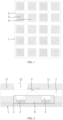
FIG. 1 is a top view of a plurality of display units of a display panel provided in an embodiment of the present application. -
FIG. 2 is a sectional view of a display panel provided in an embodiment of the present application. -
FIG. 3 is another sectional view of a display panel provided in an embodiment of the present application. -
FIG. 4 is a structural schematic diagram illustrating a display apparatus provided in an embodiment of the present application. - The technical solutions in the embodiments of the present application will be clearly and completely described below with reference to appended drawings of the embodiments of the present application. Obviously, the described embodiments are merely a part of embodiments of the present application and are not all of the embodiments. Based on the embodiments of the present application, all the other embodiments obtained by those of ordinary skill in the art without making any inventive effort are within the scope the present application.
- In the description of the present application, it is to be understood that the terms "center", "longitudinal", "lateral", "length", "width", "thickness", "upper", "lower", "front", "rear", "left", "right", "vertical", "horizontal", "top", "bottom", "inner", "outer", "clockwise", "counterclockwise" and the like indicated orientation or positional relationship are based on the relationship of the position or orientation shown in the drawings, which is only for the purpose of facilitating description of the present application and simplifying the description, but is not intended to or implied that the device or element referred to must have a specific orientation, and be constructed and operated in a particular orientation. Therefore, it should not be construed as a limitation of the present application. In addition, the terms "first" and "second" are used for descriptive purposes only, and should not be taken to indicate or imply relative importance, or implicitly indicate the indicated number of technical features. Thus, by defining a feature with "first" or "second", it may explicitly or implicitly include one or more features. In the description of the present application, "a plurality" means two or more unless explicitly defined.
- In the description of the present application, it should be noted that unless otherwise explicitly specified or limited, the terms "installed", "connected", and "connection" should be construed broadly, for example, a fixed connection, a removable connection, or integrally connected. These terms may be directed to a mechanical connection, and may also be directed to an electrical connection or communication. Moreover, these terms can be directed to "directly attached", "indirectly connected" through an intermediate medium, and may be directed to "internally communicated" with two components or the "interaction relationship" between two components. For persons skilled in the art, they can understand the specific meaning of the terms in the present application based on specific conditions.
- In the present application, unless specified or limited otherwise, a structure in which a first feature is "on" or "below" a second feature may include an embodiment in which the first feature is in direct contact with the second feature, and may also include an embodiment in which the first feature and the second feature are not in direct contact with each other, but are contacted via an additional feature formed therebetween. Furthermore, a first feature "on," "above," or "on top of" a second feature may include an embodiment in which the first feature is right or obliquely "on," "above," or "on top of" the second feature, or just means that the first feature is at a height higher than that of the second feature; while a first feature "below," "under," or "on bottom of" a second feature may include an embodiment in which the first feature is right or obliquely "below," "under," or "on bottom of" the second feature, or just means that the first feature is at a height lower than that of the second feature.
- The following disclosure provides a plurality of different embodiments or examples to implement different structures of this application. To simplify the disclosure of this application, the following describes components and settings in particular examples. Certainly, the examples are merely for illustrative purposes, and are not intended to limit this application. In addition, in this application, reference numerals and/or reference letters may be repeated in different examples. This repetition is for the purpose of simplicity and clarity, and does not in itself indicate a relationship between the various embodiments and/or settings that are discussed. In addition, this application provides examples of various particular processes and materials, but a person of ordinary skill in the art will recognize that other processes and/or materials may be applied and/or used.
- Traditional brightness compensation (Demura) includes the following major steps: activating a display panel by a driving chip to display several pictures (usually with grayscales or RGB); using a high-resolution and high-precision charge-coupled device (CCD) camera to shoot the aforesaid pictures; analyzing a color distribution of subpixels based on data collected by the camera and identifying Mura based on relevant algorithms; generating brightness compensation data based on actual brightness data, predetermined brightness data and a corresponding brightness compensation algorithm; and burning or writing the brightness compensation data to a flash ROM and performing brightness compensation on the display panel based on the brightness compensation data, and reshooting a compensated picture to confirm that Mura has been eliminated.
- The traditional brightness compensation requires sophisticated peripheral equipments (e.g., AOI) and this makes the compensation more complicated. In addition, the traditional brightness compensation is restricted to be used in a factory of a display panel manufacturer, and uneven brightness caused by device aging brought during repeated use of the display panel, cannot be compensated for the second time. This reduces reliability of the products to a certain extent. Therefore, there is an urgent need to develop a technology that enables brightness compensation performed on the display panel in real time.
- As shown in
FIGs. 1 and 2 , an embodiment of the present application provides adisplay panel 1, which includes a plurality ofdisplay units 2 arranged in an array. Eachdisplay unit 2 includes adisplay device 3 and aphotosensitive device 4 arranged in a same layer. Alight reflecting unit 5 is provided at a side of each display unit 2 (thelight reflecting unit 5 is located at a light emitting side of the display unit 2) and is configured to partially reflect light emitted by thedisplay device 3, to thephotosensitive device 4 to detect the light emitted by thedisplay device 3 to obtain brightness data. - Specifically, the
display device 3 includes an organic electroluminescent device (e.g., an OLED). Of course, it can also be a micro light-emitting diode (micro LED) or of any other type of display device, and it is not limited herein. Thephotosensitive device 4 includes any of an organic photodiode (OPD), an amorphous silicon device and a complementary metal oxide semiconductor device. Of course, it can also be another photosensitive device capable of transforming a light signal into an electrical signal, and it is not limited herein. A material of thelight reflecting unit 5 may include a light reflecting metal material. - Specifically, the photosensitive device can transform a received light signal into an electrical signal so as to detect the light emitted by a
corresponding display device 3 to obtain its corresponding brightness data. It should be noted that a correspondence exists between the brightness data and the electrical signal, and various levels of electrical signals correspond to different brightness data. Therefore, the brightness data detected by thephotosensitive device 4 is directed to actual brightness of the light emitted by thedisplay device 3. Based on an analysis of and a comparison between the brightness data and a predetermined brightness data (which is the brightness displayed in a normal state), it can be determined whether there is a brightness difference, that is, whether there is Mura. It can provide a reliable basis for the brightness compensation. - Specifically, each
display unit 2 further includes aspacer unit 6 located between thedisplay device 3 and thephotosensitive device 4. Thelight reflecting unit 5 is disposed corresponding to thespacer unit 6. A thin-film encapsulating layer 7 is also provided between thelight reflecting unit 5 and thedisplay unit 2, and is configured to protect thedisplay device 3 and thephotosensitive device 4. As shown inFIG. 3 , the thin-film encapsulating layer 7 includes a firstinorganic encapsulating layer 8, anorganic encapsulating layer 9 and a secondinorganic encapsulating layer 10 sequentially disposed on thedisplay unit 2. Of course, thespacer unit 6 is also provided between any twoadjacent display units 2. A material of thespacer unit 6 includes a photoresist material. - Specifically, a
light shielding unit 11 is also disposed at a side of eachlight reflecting unit 5 away from thespacer unit 6. A material of thelight shielding unit 11 includes a material of a black color filter. In an embodiment, thelight shielding unit 11 is also disposed corresponding to thephotosensitive device 4, in order to prevent ambient light from interfering with thephotosensitive device 4. It facilitates improving accuracy of the detected brightness data. - Specifically, as shown in
FIG. 3 , a first thin-film transistor 13 and a second thin-film transistor 14 are disposed at a side of eachdisplay unit 2 away from thelight reflecting unit 5. The first thin-film transistor 13 is connected to thedisplay device 3 and is configured to control operations of thedisplay device 3. The second thin-film transistor 14 is connected to thephotosensitive device 4 and is configured to output the brightness data. - Specifically, the
display device 3 includes afirst anode 15, and a light-emittingfunctional layer 16 and acathode 17 sequentially disposed on thefirst anode 15. Thephotosensitive device 4 includes asecond anode 18, and a photosensitivefunctional layer 19 and thecathode 17 sequentially disposed on thesecond anode 18. Thefirst anode 15 and thesecond anode 18 have a same material, and thedisplay device 3 and thephotosensitive device 4 share asame cathode 17. The first thin-film transistor 13 includes afirst source 20, afirst drain 21, afirst gate 22 and a firstactive layer 23, in which thefirst drain 21 and thefirst anode 15 are connected to each other via a via hole. The second thin-film transistor 14 includes asecond source 24, asecond drain 25, asecond gate 26 and a secondactive layer 27, in which thesecond drain 25 and thesecond anode 18 are connected to each other via a via hole. Thefirst source 20, thefirst drain 21, thesecond source 24 and thesecond drain 25 may be manufactured using a same material in a same manufacturing process. Thefirst gate 22 and thesecond gate 26 may be manufactured using a same material in a same manufacturing process. The firstactive layer 23 and the secondactive layer 27 may be manufactured using a same material in a same manufacturing process. - Specifically, the
display panel 1 further includes asubstrate 28 and a water andoxygen blocking layer 29 disposed on thesubstrate 28. The first thin-film transistor 13 and the second thin-film transistor 14 are located on the water andoxygen blocking layer 29. Thedisplay panel 1 further includes agate insulating layer 30 disposed between thefirst gate 22 and the first active layer 23 (or between thesecond gate 26 and the second active layer 27), an insulatinginterlayer 31 disposed between thefirst gate 22, and thefirst source 20 and the first drain 21 (or between thesecond gate 26, and thesecond source 24 and the second drain 25), and aflattening layer 32 disposed between thefirst source 20 and thefirst drain 21, and the first anode 15 (or between thesecond source 24 and thesecond drain 25, and the second anode 18). Thespacer unit 6 is disposed on theflattening layer 32 and partially covers thefirst anode 15 and thesecond anode 18. - Compared to obtaining actual brightness of the
display panel 1 by sophisticated peripheral equipments in existing arts, the embodiment of the present application integrates thephotosensitive device 4 and thedisplay device 3 of eachdisplay unit 2 into asame display panel 1. In the present embodiment, eachdisplay device 3 corresponds to onephotosensitive device 4, and by a correspondinglight reflecting unit 5, it can partially reflect the light emitted by eachdisplay device 3, to a correspondingphotosensitive device 4 to obtain brightness data of the light emitted by eachdisplay device 3. The brightness data of eachdisplay unit 2 can be obtained without a need to use the sophisticated peripheral equipments. It is convenient in operation. Also, during use of thedisplay panel 1, it can detect in real time whether the brightness of eachdisplay unit 2 is abnormal, providing a reliable basis for brightness compensation. - In an embodiment, a
light transmitting unit 12 is disposed at a side of eachdisplay unit 2 and is disposed corresponding to thedisplay device 3. Thelight transmitting unit 12 and thelight shielding unit 11 are arranged in a same layer. Specifically, thelight transmitting unit 12 has a property of selective transmission for light waves and plays a role of light filtering.Different display devices 3 may emit various colors of light, such as red light, green light and blue light. Correspondingly, thelight transmitting unit 12 corresponding to thedisplay device 3 emitting the red light only allows the red light to pass; thelight transmitting unit 12 corresponding to thedisplay device 3 emitting the green light only allows the green light to pass; thelight transmitting unit 12 corresponding to thedisplay device 3 emitting the blue light only allows the blue light to pass. Thelight transmitting unit 12 and thelight shielding unit 11 constitute a color filter, which substitutes an original polarizer, that is, it is directed to a POL-Less technology, which is beneficial to reduce the thickness of thedisplay panel 1. - In an embodiment, a surface side of the
light reflecting unit 5 close to the spacer layer is a concave arc surface such that onephotosensitive device 4 only receives a light signal emitted by one correspondingdisplay device 3. This prevents thephotosensitive device 4 from being interfered with or affected by the light signals emitted by otheradjacent display devices 3. It facilitates improving accuracy of the brightness data. - As shown in
FIG. 4 , an embodiment of the present application further provides adisplay apparatus 33, which includes thedisplay panel 1 according to above embodiments, abrightness compensation module 34 and adriving module 35. Thebrightness compensation module 34 is connected to thephotosensitive device 4 of eachdisplay unit 2 and is configured to obtain the brightness data and output brightness compensation data based on the brightness data. The drivingmodule 35 has one end connected to thebrightness compensation module 34 and another end connected to the display panel, and is configured to perform brightness compensation on thedisplay panel 1 based on the brightness compensation data. Specifically, the brightness compensation is performed on thedisplay panel 1 for thedisplay units 2 having uneven brightness, based on the brightness compensation data. - Specifically, after converting a light signal into an electrical signal, the
photosensitive device 4 of eachdisplay unit 2 outputs the electrical signal to thebrightness compensation module 34 by a corresponding second thin-film transistor 14. After obtaining the brightness data corresponding to eachdisplay unit 2, thebrightness compensation module 34 performs an analysis based on predetermined brightness data (which is the brightness displayed in a normal state) of eachdisplay unit 2 to determine whether there is a brightness difference for eachdisplay unit 2, that is, performing a Mura recognition on thedisplay panel 1. After that, brightness compensation data is outputted by use of a corresponding Demura compensation algorithm in accompanying with a driving current of thedisplay panel 1. - Specifically, the
display apparatus 33 further includes astoring module 36 such as a flash ROM. The storingmodule 36 has one end connected to thebrightness compensation module 34 and another end connected to thedriving module 35. The brightness compensation data outputted by thebrightness compensation module 34 may be directly burned or written to thestoring module 36. The drivingmodule 35 includes a drive IC. The drivingmodule 35 may directly read the brightness compensation data from the storingmodule 36 and perform the brightness compensation on thedisplay unit 2 of thedisplay panel 1 based on the brightness compensation data. - Specifically, the brightness compensation data includes position information and a compensation value for a to-
be-compensated display unit 2. It should be noted that the brightness compensation data may include the position information and the compensation value for eachdisplay unit 2 and meanwhile, the compensation value for adisplay unit 2 that displays normally can be set as zero. Of course, the brightness compensation data may include only the position information and the compensation value for adisplay unit 2 having uneven brightness, and the present application is not limited herein. - Specifically, the
brightness compensation module 34, the storingmodule 36 and the drivingmodule 35 may be integrated on a same circuit board to reduce the size of thedisplay apparatus 33. - Specifically, the
display apparatus 33 of the present embodiment can perform, in real time, brightness data measurement, Mura recognition and brightness compensation to obtain a display effect of uniform brightness. Also, eachdisplay unit 2 of thedisplay panel 1 that has been performed with the brightness compensation may be detected once again so as to estimate a result of the compensation. It can also perform the brightness compensation on thedisplay panel 1 for many times eventually to achieve uniform brightness displaying. The present embodiment can perform the brightness compensation on thedisplay panel 1 with a need to use peripheral equipments, and can perform the brightness compensation on thedisplay panel 1 anywhere anytime. It is convenient in operation. - In the present embodiment, the
brightness compensation module 34 can analyze the brightness of each display device based on the brightness data outputted by eachphotosensitive device 4, and obtain a corresponding brightness compensation data by use of a compensation algorithm. The drivingmodule 35 can perform the brightness compensation on acorresponding display unit 2 based on the brightness compensation data to achieve uniform brightness displaying. The brightness compensation can be performed in real time during use of thedisplay apparatus 33, and brightness data detection and brightness compensation can be performed for many times. It ensures uniform brightness displaying, and improves reliability ofdisplay panel 1 performance, that is, improving reliability ofdisplay apparatus 33 performance. - In the above embodiments, different emphasis is placed on respective embodiments, and reference may be made to related depictions in other embodiments for portions not detailed in a certain embodiment.
- Hereinbefore, the display panel and the display apparatus provided in the embodiments of the present application are introduced in detail, the principles and implementations of the present application are set forth herein with reference to specific examples, descriptions of the above embodiments are merely served to assist in understanding the technical solutions and essential ideas of the present application. Those having ordinary skill in the art should understand that they still can modify technical solutions recited in the aforesaid embodiments or equivalently replace partial technical features therein; these modifications or substitutions do not make essence of corresponding technical solutions depart from the spirit and scope of technical solutions of embodiments of the present application.
Claims (20)
- A display panel, comprising a plurality of display units arranged in an array, each of the display units comprising: a display device and a photosensitive device arranged in a same layer,
wherein a light reflecting unit is provided at a side of each of the display units and is configured to partially reflect light emitted by the display device, to the photosensitive device to detect the light emitted by the display device to obtain brightness data. - The display panel according to claim 1, wherein each of the display units further includes a spacer unit located between the display device and the photosensitive device, and the light reflecting unit is disposed corresponding to the spacer unit.
- The display panel according to claim 2, further comprising a light shielding unit disposed at a side of the light reflecting unit away from the spacer unit.
- The display panel according to claim 3, wherein the light shielding unit is disposed corresponding to the photosensitive device.
- The display panel according to claim 3, further comprising a light transmitting unit disposed at a side of each of the display units and disposed corresponding to the display device, wherein the light transmitting unit and the light shielding unit are disposed at a same layer.
- The display panel according to claim 2, wherein a side surface of the light reflecting unit close to the spacer layer is a concave arc surface.
- The display panel according to claim 1, wherein the photosensitive device comprises any of an organic photodiode, an amorphous silicon device and a complementary metal oxide semiconductor device.
- The display panel according to claim 1, wherein the display device comprises an organic electroluminescent diode.
- The display panel according to claim 1, further comprising a first thin-film transistor and a second thin-film transistor disposed at a side of each of the display units away from the light reflecting unit, wherein the first thin-film transistor is connected to the display device and the second thin-film transistor is connected to the photosensitive device.
- A display panel, comprising a plurality of display units arranged in an array, each of the display units comprising: a display device, a photosensitive device and a spacer unit disposed between the display device and the photosensitive device, wherein the display device, the photosensitive device and the spacer unit are arranged in a same layer;a light reflecting unit disposed at a side of each of the display units and disposed corresponding to the spacer unit, wherein a side surface of the light reflecting unit close to the spacer layer is a concave arc surface and the light reflecting unit is configured to partially reflect light emitted by the display device, to the photosensitive device to detect the light emitted by the display device to obtain brightness data;a light shielding unit disposed at a side of the light reflecting unit away from the spacer unit; and a light transmitting unit disposed at a side of each of the display units and disposed corresponding to the display device, wherein the light transmitting unit and the light shielding unit are disposed at a same layer.
- A display apparatus, comprising the display panel according to claim 1, a brightness compensation module and a driving module;the brightness compensation module connected to the photosensitive device of each of the display units and configured to obtain the brightness data and output brightness compensation data based on the brightness data; andthe driving module having one end connected to the brightness compensation module and another end connected to the display panel, configured to perform brightness compensation on the display panel based on the brightness compensation data.
- The display apparatus according to claim 11, further comprising a storing module, wherein one end of the storing module is connected to the brightness compensation module and another end of the storing module is connected to the driving module.
- The display apparatus according to claim 11, wherein each of the display units further includes a spacer unit located between the display device and the photosensitive device, and the light reflecting unit is disposed corresponding to the spacer unit.
- The display apparatus according to claim 13, further comprising a light shielding unit disposed at a side of the light reflecting unit away from the spacer unit.
- The display apparatus according to claim 14, wherein the light shielding unit is disposed corresponding to the photosensitive device.
- The display apparatus according to claim 14, further comprising a light transmitting unit disposed at a side of each of the display units and disposed corresponding to the display device, wherein the light transmitting unit and the light shielding unit are disposed at a same layer.
- The display apparatus according to claim 13, wherein a side surface of the light reflecting unit close to the spacer layer is a concave arc surface.
- The display apparatus according to claim 11, wherein the photosensitive device comprises any of an organic photodiode, an amorphous silicon device and a complementary metal oxide semiconductor device.
- The display apparatus according to claim 11, wherein the display device comprises an organic electroluminescent diode.
- The display apparatus according to claim 11, further comprising a first thin-film transistor and a second thin-film transistor disposed at a side of each of the display units away from the light reflecting unit, wherein the first thin-film transistor is connected to the display device and the second thin-film transistor is connected to the photosensitive device.
Applications Claiming Priority (2)
| Application Number | Priority Date | Filing Date | Title |
|---|---|---|---|
| CN202010341702.1A CN111524943A (en) | 2020-04-27 | 2020-04-27 | Display panel and display device |
| PCT/CN2020/097387 WO2021217836A1 (en) | 2020-04-27 | 2020-06-22 | Display panel and display apparatus |
Publications (2)
| Publication Number | Publication Date |
|---|---|
| EP4145522A1 true EP4145522A1 (en) | 2023-03-08 |
| EP4145522A4 EP4145522A4 (en) | 2024-05-22 |
Family
ID=71911140
Family Applications (1)
| Application Number | Title | Priority Date | Filing Date |
|---|---|---|---|
| EP20911298.6A Pending EP4145522A4 (en) | 2020-04-27 | 2020-06-22 | DISPLAY BOARD AND DISPLAY DEVICE |
Country Status (4)
| Country | Link |
|---|---|
| US (1) | US20220139308A1 (en) |
| EP (1) | EP4145522A4 (en) |
| CN (1) | CN111524943A (en) |
| WO (1) | WO2021217836A1 (en) |
Families Citing this family (6)
| Publication number | Priority date | Publication date | Assignee | Title |
|---|---|---|---|---|
| CN112201167A (en) * | 2020-10-30 | 2021-01-08 | 湖北长江新型显示产业创新中心有限公司 | Display panel, driving method thereof and display device |
| CN112310328B (en) * | 2020-11-02 | 2023-04-07 | 京东方科技集团股份有限公司 | Light-emitting panel and light-emitting device |
| CN114264323A (en) * | 2021-12-14 | 2022-04-01 | 武汉华星光电半导体显示技术有限公司 | Optical sensor and display panel |
| CN114530481A (en) * | 2022-02-18 | 2022-05-24 | 京东方科技集团股份有限公司 | Display panel, manufacturing method thereof, brightness compensation method and display device |
| CN114709249B (en) * | 2022-03-29 | 2025-02-14 | 武汉华星光电半导体显示技术有限公司 | Display panel and display device |
| CN114823816A (en) * | 2022-04-02 | 2022-07-29 | 武汉华星光电半导体显示技术有限公司 | Display panel and display device |
Family Cites Families (15)
| Publication number | Priority date | Publication date | Assignee | Title |
|---|---|---|---|---|
| JP3872810B1 (en) * | 2005-08-12 | 2007-01-24 | シャープ株式会社 | Light source control device, illumination device, and liquid crystal display device |
| JP2012226168A (en) * | 2011-04-20 | 2012-11-15 | Funai Electric Co Ltd | Image display device |
| JP2014194517A (en) * | 2013-02-27 | 2014-10-09 | Sony Corp | Display device, manufacturing method of the display device, drive method of the display device and electronic apparatus |
| CN105867696B (en) * | 2016-06-03 | 2020-11-17 | 京东方科技集团股份有限公司 | Touch display panel, flexible display panel and display device |
| CN106229331B (en) * | 2016-08-31 | 2019-03-29 | 上海箩箕技术有限公司 | Self-luminous display pixel |
| CN106297679B (en) * | 2016-09-19 | 2017-09-15 | 京东方科技集团股份有限公司 | Display device and the method for controlling display device brightness |
| CN107425038B (en) * | 2017-06-09 | 2020-01-21 | 武汉天马微电子有限公司 | An organic light-emitting display panel, a method for manufacturing the same, and an electronic device |
| CN107546337B (en) * | 2017-08-24 | 2020-07-24 | 京东方科技集团股份有限公司 | Organic light emitting device, brightness adjusting method thereof and display device |
| CN110164362B (en) * | 2018-06-26 | 2021-08-17 | 京东方科技集团股份有限公司 | Compensation device and method for light-emitting device, display substrate and manufacturing method thereof |
| WO2020068057A1 (en) * | 2018-09-25 | 2020-04-02 | Carl Zeiss Industrielle Messtechnik Gmbh | Multi-color surface inspection system, method for inspecting a surface, and method for calibrating the multi-color surface inspection system |
| KR102687203B1 (en) * | 2018-10-01 | 2024-07-19 | 엘지디스플레이 주식회사 | Display apparatus including light rpceving pixel area |
| CN109638047B (en) * | 2018-12-13 | 2020-12-22 | 京东方科技集团股份有限公司 | Display panel, method of making the same, and method of driving the display panel |
| KR20200109437A (en) * | 2019-03-12 | 2020-09-23 | 삼성디스플레이 주식회사 | Electronic panel and electronic apparatus including the same |
| CN110310588A (en) * | 2019-06-27 | 2019-10-08 | 昆山国显光电有限公司 | A kind of display device |
| KR102932292B1 (en) * | 2019-11-28 | 2026-03-03 | 삼성디스플레이 주식회사 | Display device having fingerprint sensing function and operating method thereof |
-
2020
- 2020-04-27 CN CN202010341702.1A patent/CN111524943A/en active Pending
- 2020-06-22 EP EP20911298.6A patent/EP4145522A4/en active Pending
- 2020-06-22 WO PCT/CN2020/097387 patent/WO2021217836A1/en not_active Ceased
- 2020-06-22 US US17/253,117 patent/US20220139308A1/en not_active Abandoned
Also Published As
| Publication number | Publication date |
|---|---|
| US20220139308A1 (en) | 2022-05-05 |
| WO2021217836A1 (en) | 2021-11-04 |
| CN111524943A (en) | 2020-08-11 |
| EP4145522A4 (en) | 2024-05-22 |
Similar Documents
| Publication | Publication Date | Title |
|---|---|---|
| EP4145522A1 (en) | Display panel and display apparatus | |
| US8599223B2 (en) | Display device, method for correcting luminance degradation, and electronic apparatus | |
| US20220172684A1 (en) | Light emitting display device and driving method thereof | |
| US8810554B2 (en) | Display device and electronic product | |
| EP4024380B1 (en) | Display substrate and display panel | |
| US8368677B2 (en) | Optical sensor device, display apparatus, and method for driving optical sensor device | |
| US11508942B2 (en) | OLED display substrate and manufacturing method thereof, OLED display device, and brightness compensation method | |
| US20080259051A1 (en) | Display device and electronic apparatus | |
| US20210233984A1 (en) | Array substrate and fabrication method thereof, and display device | |
| US8212798B2 (en) | Display device and electronic product | |
| US8723847B2 (en) | Display device and electronic product | |
| US20100149079A1 (en) | Display device, method of driving display device, and electronic apparatus | |
| US20100118003A1 (en) | Display device and electronic product | |
| JP2022021645A (en) | Display | |
| US10971570B2 (en) | Display device and brightness detection method therefor | |
| TW201818387A (en) | Current compensation method and component for electroluminescent display | |
| US11849604B2 (en) | Display device and pixel array substrate thereof | |
| US11393394B2 (en) | Compensation method and compensation apparatus for organic light-emitting display and display device | |
| JP4702395B2 (en) | Display device and electronic device | |
| US12477912B2 (en) | Display panel and display apparatus | |
| JP2009258414A (en) | Display device, its manufacturing method, and electronic device | |
| JP2009272577A (en) | Thin film transistor, method of manufacturing thin film transistor, and display device | |
| JP2009302272A (en) | Semiconductor device, manufacturing method of semiconductor device, display, and electronic apparatus |
Legal Events
| Date | Code | Title | Description |
|---|---|---|---|
| STAA | Information on the status of an ep patent application or granted ep patent |
Free format text: STATUS: UNKNOWN |
|
| STAA | Information on the status of an ep patent application or granted ep patent |
Free format text: STATUS: THE INTERNATIONAL PUBLICATION HAS BEEN MADE |
|
| PUAI | Public reference made under article 153(3) epc to a published international application that has entered the european phase |
Free format text: ORIGINAL CODE: 0009012 |
|
| STAA | Information on the status of an ep patent application or granted ep patent |
Free format text: STATUS: REQUEST FOR EXAMINATION WAS MADE |
|
| 17P | Request for examination filed |
Effective date: 20210712 |
|
| AK | Designated contracting states |
Kind code of ref document: A1 Designated state(s): AL AT BE BG CH CY CZ DE DK EE ES FI FR GB GR HR HU IE IS IT LI LT LU LV MC MK MT NL NO PL PT RO RS SE SI SK SM TR |
|
| DAV | Request for validation of the european patent (deleted) | ||
| DAX | Request for extension of the european patent (deleted) | ||
| REG | Reference to a national code |
Ref country code: DE Ref legal event code: R079 Free format text: PREVIOUS MAIN CLASS: H01L0027320000 Ipc: H10K0059130000 |
|
| A4 | Supplementary search report drawn up and despatched |
Effective date: 20240424 |
|
| RIC1 | Information provided on ipc code assigned before grant |
Ipc: G09G 3/3208 20160101ALN20240418BHEP Ipc: H10K 59/13 20230101AFI20240418BHEP |