EP4145493A1 - Formation method for connecting pad, and semiconductor structure - Google Patents
Formation method for connecting pad, and semiconductor structure Download PDFInfo
- Publication number
- EP4145493A1 EP4145493A1 EP21881347.5A EP21881347A EP4145493A1 EP 4145493 A1 EP4145493 A1 EP 4145493A1 EP 21881347 A EP21881347 A EP 21881347A EP 4145493 A1 EP4145493 A1 EP 4145493A1
- Authority
- EP
- European Patent Office
- Prior art keywords
- layer
- forming
- pattern definition
- mask
- group
- Prior art date
- Legal status (The legal status is an assumption and is not a legal conclusion. Google has not performed a legal analysis and makes no representation as to the accuracy of the status listed.)
- Granted
Links
Images






Classifications
-
- H—ELECTRICITY
- H10—SEMICONDUCTOR DEVICES; ELECTRIC SOLID-STATE DEVICES NOT OTHERWISE PROVIDED FOR
- H10P—GENERIC PROCESSES OR APPARATUS FOR THE MANUFACTURE OR TREATMENT OF DEVICES COVERED BY CLASS H10
- H10P50/00—Etching of wafers, substrates or parts of devices
- H10P50/71—Etching of wafers, substrates or parts of devices using masks for conductive or resistive materials
-
- H—ELECTRICITY
- H10—SEMICONDUCTOR DEVICES; ELECTRIC SOLID-STATE DEVICES NOT OTHERWISE PROVIDED FOR
- H10P—GENERIC PROCESSES OR APPARATUS FOR THE MANUFACTURE OR TREATMENT OF DEVICES COVERED BY CLASS H10
- H10P76/00—Manufacture or treatment of masks on semiconductor bodies, e.g. by lithography or photolithography
- H10P76/40—Manufacture or treatment of masks on semiconductor bodies, e.g. by lithography or photolithography of masks comprising inorganic materials
- H10P76/408—Manufacture or treatment of masks on semiconductor bodies, e.g. by lithography or photolithography of masks comprising inorganic materials characterised by their sizes, orientations, dispositions, behaviours or shapes
-
- H—ELECTRICITY
- H10—SEMICONDUCTOR DEVICES; ELECTRIC SOLID-STATE DEVICES NOT OTHERWISE PROVIDED FOR
- H10P—GENERIC PROCESSES OR APPARATUS FOR THE MANUFACTURE OR TREATMENT OF DEVICES COVERED BY CLASS H10
- H10P76/00—Manufacture or treatment of masks on semiconductor bodies, e.g. by lithography or photolithography
- H10P76/40—Manufacture or treatment of masks on semiconductor bodies, e.g. by lithography or photolithography of masks comprising inorganic materials
- H10P76/408—Manufacture or treatment of masks on semiconductor bodies, e.g. by lithography or photolithography of masks comprising inorganic materials characterised by their sizes, orientations, dispositions, behaviours or shapes
- H10P76/4085—Manufacture or treatment of masks on semiconductor bodies, e.g. by lithography or photolithography of masks comprising inorganic materials characterised by their sizes, orientations, dispositions, behaviours or shapes characterised by the processes involved to create the masks
-
- H—ELECTRICITY
- H10—SEMICONDUCTOR DEVICES; ELECTRIC SOLID-STATE DEVICES NOT OTHERWISE PROVIDED FOR
- H10D—INORGANIC ELECTRIC SEMICONDUCTOR DEVICES
- H10D1/00—Resistors, capacitors or inductors
- H10D1/60—Capacitors
- H10D1/68—Capacitors having no potential barriers
Definitions
- the present disclosure relates to the technical field of methods for fabricating semiconductor memory devices, and more particularly, to a method for forming a connecting pad and a semiconductor structure.
- a hole corresponding to the connecting pad changes from an original parallelogram to an ellipse and is transferred downward. Due to an etching load effect, a top of the hole is constantly subjected to plasma effect and shaped like a relatively regular circle. A near-bottom of the hole is primarily subjected to bombardment of an etching gas, causing the bottom of the hole to maintain its original elliptical shape, so the connecting pad is shaped like an oval.
- One aspect of embodiments of the present disclosure provides a method for forming a connecting pad, wherein the method includes: providing a substrate; sequentially forming a conductive layer, a first pattern definition layer and a second pattern definition layer on a surface of the substrate; sequentially forming a first group of patterns, a second group of patterns, and a third group of patterns intersecting with each other at 120° on the second pattern definition layer, an intersection portion of the three groups of patterns forming a hexagonal pattern definition structure on the second pattern definition layer; transferring the pattern definition structure downward, and etching away a portion of the first pattern definition layer, such that the remaining first pattern definition layer forms a columnar structure, wherein a bottom of the columnar structure is circular in shape under an action of an etching load effect; and etching the conductive layer by the remaining first pattern definition layer as a mask, such that the remaining conductive layer forms a circular connecting pad.
- Another aspect of the embodiments of the present disclosure provides a semiconductor structure having a connecting pad, the connecting pad is formed by means of the method for forming a connecting pad according to the present disclosure and described in the above-mentioned embodiments.
- FIG. 1 to FIG. 3 , FIG. 5 to FIG. 8 , FIG. 10 to FIG. 13 , FIG. 15 and FIG. 17 schematic structural diagrams of a semiconductor structure in some steps of a method for forming a connecting pad according to the present disclosure are typically illustrated, respectively.
- this method for forming a connecting pad according to the present disclosure is described by means of an example where an immersion lithography process is employed to form a capacitor of a semiconductor structure.
- the method for forming a connecting pad according to the present disclosure includes:
- a hexagonal first hole h1 is formed by means of a triple exposure process.
- the columnar structure defining the connection pad 210 is transformed from a hexagonal straight edge profile at the top to a circular arc to form a relatively regular circle, such that the shape of the connection pad 210 is significantly improved.
- the present disclosure can ensure that the connecting pad 210 is circular, such that the connecting pad 210 has a larger margin during a capacitor patterning process, and it can be stopped on the connecting pad 210 during etching, thus avoiding a problem of capacitor leakage caused by breakdown.
- the step of forming a first pattern definition layer 300 on a surface of the conductive layer 200 may include:
- a pattern transfer layer 400 may also be formed between the first pattern definition layer 300 and the second pattern definition layers 500. In this way, reverse selective etching during the downward transfer of the first hole h1 of the second pattern definition layer 500 is implemented.
- the formation of the pattern transfer layer 400 may include the following steps:
- the processes in the step of pattern reverse selective etching will be described in the following content in the order of the processes and the drawings. It should be noted that in other embodiments, to allow the first hole h1 of the second pattern definition layer 500 to transfer to the first pattern definition layer 300 by means of reverse selective etching to form the second columnar structure 330, it is also advisable that the pattern transfer layer in this embodiment is not provided. That is, the formation of the second columnar structure 330 may be implemented by other processes and is not limited to this embodiment.
- the step of forming a second pattern definition layer 500 on a surface of the pattern transfer layer 400 may include:
- the step of forming a first group of trenches G1 on the second pattern definition layer 500 may include:
- the step of forming a first mask layer 610 on the surface of the second pattern definition layer 500 may include:
- the step of forming a first trench structure 631 on a surface of the first mask layer 610 by means of a pitch multiplication process may include:
- the semiconductor structure in the step of forming a third sacrificial layer 630 on the surface of the first mask layer 610 and a surface of the first photoresist layer 620 is typically illustrated.
- the semiconductor structure includes the substrate 100, the conductive layer 200, the first pattern definition layer 300, the pattern transfer layer 400, the second pattern definition layer 500, the first mask layer 610, the patterned first photoresist layer 620, and the third sacrificial layer 630.
- the conductive layer 200 is formed on the surface of the substrate 100.
- the first pattern definition layer 300 is formed on the surface of the conductive layer 200, wherein the first pattern definition layer 300 sequentially includes the first passivation layer 310 and the first sacrificial layer 320.
- the pattern transfer layer 400 is formed on the surface of the first sacrificial layer 320, wherein the pattern transfer layer 400 sequentially includes the polysilicon contact layer 410 and the second sacrificial layer 420.
- the second pattern definition layer 500 is formed on the surface of the second sacrificial layer 420, and includes the second passivation layer 510 and the first anti-reflection layer 520.
- the first mask layer 610 is formed on the surface of the second pattern definition layer 500, and includes the third passivation layer 611 and the second anti-reflection layer 612.
- the first photoresist layer 620 is formed on the surface of the first mask layer 610, and the first photoresist layer 620 is patterned to form the first opening 621.
- the third sacrificial layer 630 is formed on the surface of the first mask layer 610 and the surface of the remaining first photoresist layer 620. That is, the third sacrificial layer 630 covers the surface of the first mask layer 610 exposed to the first opening 621, and covers the sidewall and the bottom wall of the first opening 621.
- a material of the conductive layer 200 may include, but is not limited to, tungsten (W).
- the first passivation layer 310 may include, but is not limited to, a diamond-like carbon (DLC) coating.
- DLC diamond-like carbon
- a material of the first sacrificial layer 320 may include, but is not limited to, silicon nitride (Si 3 N 4 ).
- a material of the second sacrificial layer 420 may include, but is not limited to, silicon dioxide (SiO 2 ).
- the second passivation layer 510 may include, but is not limited to, the DLC coating.
- a material of the first anti-reflection layer 520 may include, but is not limited to, silicon oxynitride (SiON).
- the third passivation layer 611 may include, but is not limited to, the DLC coating.
- a material of the third sacrificial layer 630 may include, but is not limited to, silicon dioxide.
- a material of the second anti-reflection layer 612 may include, but is not limited to, silicon oxynitride.
- the semiconductor structure includes the substrate 100, the conductive layer 200, the first pattern definition layer 300, the pattern transfer layer 400, the second pattern definition layer 500, the first mask layer 610, and the remaining third sacrificial layer 630.
- the pitch multiplication process the portion of the third sacrificial layer 630 positioned on the surface of the first mask layer 610 and on the top surface of the first photoresist layer 620 is etched away, and the remaining third sacrificial layer 630 forms the first trench structure 631.
- the remaining first photoresist layer 620 is completely removed.
- a schematic structural diagram of the semiconductor structure in the step of transferring the first trench structure 631 to the second pattern definition layer 500 to form the first group of trenches G1 is typically illustrated.
- a plan view of the semiconductor structure in the step of transferring the first trench structure 631 to the second pattern definition layer 500 to form the first group of trenches G1 is typically illustrated.
- the semiconductor structure in this step, includes the substrate 100, the conductive layer 200, the first pattern definition layer 300, the pattern transfer layer 400, and the second pattern definition layer 500 formed with the first group of trenches G1.
- the first trench structure 631 may be transferred to the first anti-reflection layer 520 of the second pattern definition layer 500 by means of a dry etching process, such that the first group of trenches G1 are formed on the surface of the first anti-reflection layer 520.
- both the first trench structure 631 that is, the remaining third sacrificial layer 630
- the first mask layer 610 are completely removed.
- the step of forming a second group of trenches G2 on the second pattern definition layer 500 may include:
- the step of forming a second mask layer 710 on the surface of the second pattern definition layer 500 may include:
- the step of forming a second trench structure 731 on the surface of the second mask layer 710 by means of the pitch multiplication process may include:
- the semiconductor structure in the step of forming a second photoresist layer 720 on the second mask layer 710 is typically illustrated.
- the semiconductor structure includes the substrate 100, the conductive layer 200, the first pattern definition layer 300, the pattern transfer layer 400, the second pattern definition layer 500 formed with the first group of trenches G1, the second mask layer 710, and the patterned second photoresist layer 720.
- the second mask layer 710 is formed on the surface of the second pattern definition layer 500, and the second mask layer 710 is filled in the first group of trenches G1 on the surface of the first anti-reflection layer 520, wherein the second mask layer 710 includes the fourth passivation layer 711 and the third anti-reflection layer 712.
- the second photoresist layer 720 is formed on the surface of the second mask layer 710, and the second photoresist layer 720 is patterned to form the second opening 721.
- the fourth passivation layer 711 may be formed on the second pattern definition layer 500 by means of a spin coating process.
- a material of the third anti-reflection layer 712 may include, but is not limited to, silicon oxynitride.
- the semiconductor structure includes the substrate 100, the conductive layer 200, the first pattern definition layer 300, the pattern transfer layer 400, the second pattern definition layer 500 formed with the first group of trenches G1, the second mask layer 710, the patterned second photoresist layer 720, and the fourth sacrificial layer 730.
- the fourth sacrificial layer 730 is formed on the surface of the second mask layer 710 and the surface of the remaining second photoresist layer 720. That is, the fourth sacrificial layer 730 covers the surface of the second mask layer 710 exposed to the second opening 721, and covers the sidewall and the bottom wall of the second opening 721.
- a material of the fourth sacrificial layer 730 may include, but is not limited to, silicon dioxide.
- the semiconductor structure includes the substrate 100, the conductive layer 200, the first pattern definition layer 300, the pattern transfer layer 400, the second pattern definition layer 500 formed with the first group of trenches G1, the second mask layer 710, and the remaining fourth sacrificial layer 730.
- the pitch multiplication process the portion of the fourth sacrificial layer 730 positioned on the surface of the second mask layer 710 and on the top surface of the second photoresist layer 720 is etched away, and the remaining fourth sacrificial layer 730 forms the second trench structure 731.
- the remaining second photoresist layer 720 is completely removed.
- the semiconductor structure includes the substrate 100, the conductive layer 200, the first pattern definition layer 300, the pattern transfer layer 400, and the second pattern definition layer 500 formed with the first group of trenches G1 and the second group of trenches G2.
- the second trench structure 731 may be transferred to the first anti-reflection layer 520 of the second pattern definition layer 500 by means of a dry etching process, such that the second group of trenches G2 are formed on the surface of the first anti-reflection layer 520 having formed with the first group of trenches G1.
- both the second trench structure 731 that is, the remaining fourth sacrificial layer 730
- the second mask layer 710 are completely removed.
- an angle of 120° is formed between the first group of trenches G1 and the second group of trenches G2.
- the step of forming a third group of trenches G3 on the second pattern definition layer 500 may include:
- the step of forming a third mask layer 810 on the surface of the second pattern definition layer 500 may include:
- the step of forming a third trench structure 831 on a surface of the third mask layer 810 by means of the pitch multiplication process may include:
- the semiconductor structure in the step of forming a third photoresist layer 820 on the third mask layer 810 is typically illustrated.
- the semiconductor structure includes the substrate 100, the conductive layer 200, the first pattern definition layer 300, the pattern transfer layer 400, the second pattern definition layer 500 formed with the first group of trenches G1 and the second group of trenches G2, the third mask layer 810, and the patterned third photoresist layer 820.
- the third mask layer 810 is formed on the surface of the second pattern definition layer 500, and the third mask layer 810 is filled in the first group of trenches G1 and the second group of trenches G2 on the surface of the first anti-reflection layer 520, wherein the third mask layer 810 includes the fifth passivation layer 811 and the fourth anti-reflection layer 812.
- the third photoresist layer 820 is formed on the surface of the third mask layer 810, and the third photoresist layer 820 is patterned to form the third opening 821.
- the fifth passivation layer 811 may be formed on the second pattern definition layer 500 by means of a spin coating process.
- a material of the fourth anti-reflection layer 812 may include, but is not limited to, silicon oxynitride.
- the semiconductor structure includes the substrate 100, the conductive layer 200, the first pattern definition layer 300, the pattern transfer layer 400, the second pattern definition layer 500 formed with the first group of trenches G1 and the second group of trenches G2, the third mask layer 810, the patterned third photoresist layer 820, and the fifth sacrificial layer 830.
- the fifth sacrificial layer 830 is formed on the surface of the third mask layer 810 and the surface of the remaining third photoresist layer 820. That is, the fifth sacrificial layer 830 covers the surface of the third mask layer 810 exposed to the third opening 821, and covers the sidewall and the bottom wall of the third opening 821.
- a material of the fifth sacrificial layer 830 may include, but is not limited to, silicon dioxide.
- the semiconductor structure includes the substrate 100, the conductive layer 200, the first pattern definition layer 300, the pattern transfer layer 400, the second pattern definition layer 500 formed with the first group of trenches G1 and the second group of trenches G2, the third mask layer 810, and the remaining fifth sacrificial layer 830.
- the portion of the fifth sacrificial layer 830 positioned on the surface of the third mask layer 810 and on the top surface of the third photoresist layer 820 is etched away, and the remaining fifth sacrificial layer 830 forms the third trench structure 831. Moreover, in the above-mentioned etching process, the remaining third photoresist layer 820 is completely removed.
- the semiconductor structure includes the substrate 100, the conductive layer 200, the first pattern definition layer 300, the pattern transfer layer 400, and the second pattern definition layer 500 formed with the first group of trenches G1, the second group of trenches G2, and the third group of trenches G3.
- the third trench structure 831 may be transferred to the first anti-reflection layer 520 of the second pattern definition layer 500 by means of a dry etching process, such that the third group of trenches G3 are formed on the surface of the first anti-reflection layer 520 having formed with the first group of trenches G1 and the second group of trenches G2.
- both the third trench structure 831 that is, the remaining fifth sacrificial layer 830
- the third mask layer 810 are completely removed.
- an angle of 120° is formed between the first group of trenches G1 and the third group of trenches G3, and an angle of 120° is formed between the second group of trenches G2 and the third group of trenches G3. That is, an angle of 120° is formed between the three groups of trenches G1, G2, and G3.
- the step of transferring the first hole h1 downward, and etching away a portion of the first pattern definition layer 300 based on a reverse selection mode may include:
- the semiconductor structure in the step of etching the pattern transfer layer 400 by the second pattern definition layer 500 as a mask is typically illustrated.
- the semiconductor structure in this step, includes the substrate 100, the conductive layer 200, the first pattern definition layer 300, and the pattern transfer layer 400 formed with the second hole h2.
- the first hole h1 formed at an intersection location of the three groups of trenches G1, G2 and G3 on the first anti-reflection layer 520 is transferred to the second sacrificial layer 420 of the pattern transfer layer 400, such that the hexagonal second hole h2 is formed on the second sacrificial layer 420.
- the semiconductor structure includes the substrate 100, the conductive layer 200, the first pattern definition layer 300, the pattern transfer layer 400 formed with the second hole h2, and the sixth passivation layer 430.
- the sixth passivation layer 430 is filled in the second holes h2.
- the sixth passivation layer 430 may be formed on the surface of the second sacrificial layer 420 of the pattern transfer layer 400 where the second hole h2 is formed, and the sixth passivation layer 430 on the top of the second sacrificial layer 420 may be removed by means of, for example, a chemical mechanical polishing process. In this way, a portion of the sixth passivation layer 430 filled in the second holes h2 may be remained.
- FIG. 17 typically illustrates a schematic structural diagram of the semiconductor structure in the step of forming the first columnar structure 431
- FIG. 18 typically illustrates a plan view of the semiconductor structure in this step.
- the semiconductor structure includes the substrate 100, the conductive layer 200, the first pattern definition layer 300, the remaining pattern transfer layer 400 (that is, the polysilicon contact layer 410), and the first columnar structure 431.
- the sixth passivation layer 430 filled in the second holes h2 is remained to form the first columnar structure 431, thereby implementing reverse rotation etching of the first hole h1 of the second pattern definition layer 500. That is, a structure that is finally retained during the downward transfer of the pattern is a portion that is not sheltered by a mask (the second pattern definition layer 500).
- the semiconductor structure in the step of forming a second columnar structure 330 is typically illustrated.
- the semiconductor structure includes the substrate 100, the conductive layer 200, and the second columnar structure 330.
- the first pattern definition layer 300 is etched away by the first columnar structure 431 formed by the remaining pattern transfer layer 400 (i.e., the remaining second sacrificial layer 420) as a mask.
- the top of the second columnar structure 330 has the same shape as the first columnar structure 431, i.e., shaped like a hexagon.
- the second columnar structure 330 is transformed from a hexagonal straight edge profile at the top to a circular arc to form a relatively regular circular bottom.
- the remaining pattern transfer layer 400 is completely removed.
- FIG. 20 typically illustrates a schematic structural diagram of the semiconductor structure in the step of forming a connecting pad 210
- FIG. 21 typically illustrates a plan view of the semiconductor structure in this step.
- the semiconductor structure includes the substrate 100 and the remaining conductive layer 200.
- the portion of the conductive layer 200 not sheltered by the second columnar structure 330 is further etched downward until the remaining conductive layer 200 forms the connecting pad 210, and the shape of the connecting pad 210 is consistent with that of the bottom of the second columnar structure 330, i.e., shaped like a circle.
- the remaining first pattern definition layer 300 is completely removed.
- connection pads shown in the drawings and described in this specification are but a few examples of the many methods of forming that can employ the principles of the present disclosure. It should be clearly understood that the principles of the present disclosure are by no means limited to any detail or any step of the method of forming connection pads shown in the drawings or described in this specification.
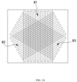
- FIG. 22 and FIG. 23 respectively show schematic structural diagrams of the semiconductor structure in some steps according to the second embodiment of this method; and FIG. 24 shows a plan view of the semiconductor structure in the step as shown in FIG. 22 .
- a process design in the second embodiment different from that in the first embodiment of the method for forming a connecting pad according to the present disclosure will be described below with reference to the accompanying drawings.
- the method for forming a connecting pad according to the present disclosure includes:
- the bulge b formed on the second pattern definition layer 500 is used, instead of the first hole in the first embodiment, as a pattern definition structure allowing the first pattern definition layer 300 to define and form the columnar structure in the subsequent steps.
- the bulge b i.e., the intersection portion of the three groups of protruding ribs B1, B2, and B3 corresponds to the remaining third columnar structure 340 of the first pattern definition layer 300. That is, the bulge b corresponds to a location of the connecting pad finally formed.
- a direct etching mode i.e., a forward selection mode
- a forward selection mode is employed when the bulge b is transferred downward.
- the method for forming a connecting pad according to the present disclosure includes:
- the semiconductor structure according to the present disclosure has a capacitor hole, and the capacitor hole of the semiconductor structure is formed by means of the method for forming a connecting pad according to the present disclosure and described in detail in the above embodiments.
- a hexagonal pattern is formed by means of a triple exposure process.
- the columnar structure defining the connection pad is transformed from a hexagonal straight edge profile at the top to a circular arc to form a relatively regular circle, such that the shape of the connection pad is significantly improved.
Landscapes
- Internal Circuitry In Semiconductor Integrated Circuit Devices (AREA)
Abstract
Description
- The present disclosure is based on and claims priority to
Chinese Patent Application No. 202110758234.2 titled "METHOD FOR FORMING CONNECTING PAD AND SEMICONDUCTOR STRUCTURE" and filed on July 5, 2021 - The present disclosure relates to the technical field of methods for fabricating semiconductor memory devices, and more particularly, to a method for forming a connecting pad and a semiconductor structure.
- In solutions for manufacturing capacitors of the existing semiconductor structures, due to exposure limits, typically two layers of photomasks are used in the current immersion photolithography process to form linear patterns in two directions. The linear patterns in the two directions enclose a blank parallelogram pattern. After dry etching, the pattern is transferred downward, and finally an array of connecting pads in a substantially hexagonal arrangement mode is formed.
- However, taking a single connecting pad as an example, during the pattern transfer process, a hole corresponding to the connecting pad changes from an original parallelogram to an ellipse and is transferred downward. Due to an etching load effect, a top of the hole is constantly subjected to plasma effect and shaped like a relatively regular circle. A near-bottom of the hole is primarily subjected to bombardment of an etching gas, causing the bottom of the hole to maintain its original elliptical shape, so the connecting pad is shaped like an oval. Dimensions of the elliptical connecting pad are not uniform in a long axis direction and a short axis direction, resulting in insufficient margin in the short axis direction during a capacitor patterning process, and it cannot be stopped on the connecting pad during etching, which may cause breakdown, thus leading to problems such as capacitor leakage.
- One aspect of embodiments of the present disclosure provides a method for forming a connecting pad, wherein the method includes: providing a substrate; sequentially forming a conductive layer, a first pattern definition layer and a second pattern definition layer on a surface of the substrate; sequentially forming a first group of patterns, a second group of patterns, and a third group of patterns intersecting with each other at 120° on the second pattern definition layer, an intersection portion of the three groups of patterns forming a hexagonal pattern definition structure on the second pattern definition layer; transferring the pattern definition structure downward, and etching away a portion of the first pattern definition layer, such that the remaining first pattern definition layer forms a columnar structure, wherein a bottom of the columnar structure is circular in shape under an action of an etching load effect; and etching the conductive layer by the remaining first pattern definition layer as a mask, such that the remaining conductive layer forms a circular connecting pad.
- Another aspect of the embodiments of the present disclosure provides a semiconductor structure having a connecting pad, the connecting pad is formed by means of the method for forming a connecting pad according to the present disclosure and described in the above-mentioned embodiments.
-
-
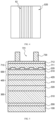
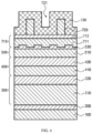
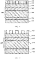
FIGS. 1 to 3 ,FIGS. 5 to 8 ,FIGS. 10 to 13 ,FIGS. 15 to 17 ,FIG. 19 andFIG. 20 respectively are schematic structural diagrams of a semiconductor structure in some steps of a method for forming a connecting pad according to the present disclosure; -
FIG. 4 ,FIG. 9 ,FIG. 14 ,FIG. 18 , andFIG. 21 respectively are plan views of the semiconductor structure in some steps of the method for forming a connecting pad according to the present disclosure; -
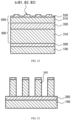
FIGS. 22 to 23 are schematic structural diagrams of the semiconductor structure in some steps of the method for forming a connecting pad according to another embodiment of the present disclosure; and -
FIG. 24 is a plan view of the semiconductor structure in the step as shown inFIG. 22 . - Exemplary embodiments will now be described more fully with reference to the accompanying drawings. However, the exemplary embodiments can be implemented in a variety of forms and should not be construed as limited to the embodiments set forth herein. Rather, these embodiments are provided such that the present disclosure will be thorough and complete and will fully convey the concepts of exemplary embodiments to those skilled in the art. Throughout the drawings, similar reference signs indicate the same or similar structures, and thus their detailed descriptions are omitted.
- Referring to
FIG. 1 to FIG. 3 ,FIG. 5 to FIG. 8 ,FIG. 10 to FIG. 13 ,FIG. 15 andFIG. 17 , schematic structural diagrams of a semiconductor structure in some steps of a method for forming a connecting pad according to the present disclosure are typically illustrated, respectively. In this exemplary embodiment, this method for forming a connecting pad according to the present disclosure is described by means of an example where an immersion lithography process is employed to form a capacitor of a semiconductor structure. It is readily comprehensible to those skilled in the art that to apply relevant design of the present disclosure to other types of capacitor structures or other processes, various modifications, additions, substitutions, deletions or other variations are made to the following embodiments, and these variations are still within the scope of the principle of the method for forming a connecting pad according to the present disclosure. - As shown in
FIG. 1 to FIG. 3 ,FIG. 5 to FIG. 8 ,FIG. 10 to FIG. 13 ,FIG. 15 to FIG. 17 ,FIG. 19 andFIG. 20 , in this embodiment, the method for forming a connecting pad according to the present disclosure includes: - providing a
substrate 100; - sequentially forming a
conductive layer 200, a firstpattern definition layer 300 and a secondpattern definition layer 500 on a surface of thesubstrate 100; - sequentially forming three groups of trenches G1, G2 and G3 intersecting with each other at 120° on the second
pattern definition layer 500, an intersection portion of the three groups of trenches forming a hexagonal first hole h1 on the secondpattern definition layer 500; - transferring the first hole h1 downward, and etching away a portion of the first
pattern definition layer 300 based on a reverse selection mode, such that the remaining firstpattern definition layer 300 forms a secondcolumnar structure 330 corresponding to the first hole h1, wherein a bottom of the secondcolumnar structure 330 is circular in shape under an action of an etching load effect; and - etching the
conductive layer 200 by the remaining firstpattern definition layer 300 as a mask, such that the remainingconductive layer 200 forms a circular connectingpad 210. - From the above description, the method for forming a connecting pad according to the present disclosure, a hexagonal first hole h1 is formed by means of a triple exposure process. In the process of transferring the first hole h1 downward, under the action of the etching load effect, the columnar structure defining the
connection pad 210 is transformed from a hexagonal straight edge profile at the top to a circular arc to form a relatively regular circle, such that the shape of theconnection pad 210 is significantly improved. By means of the above design, the present disclosure can ensure that theconnecting pad 210 is circular, such that the connectingpad 210 has a larger margin during a capacitor patterning process, and it can be stopped on the connectingpad 210 during etching, thus avoiding a problem of capacitor leakage caused by breakdown. - In some embodiments, as shown in
FIG. 1 to FIG. 3 ,FIG. 5 to FIG. 8 ,FIG. 10 to FIG. 13 ,FIG. 15 to FIG. 17 ,FIG. 19 andFIG. 20 , in this embodiment, the step of forming a firstpattern definition layer 300 on a surface of theconductive layer 200 may include: - forming a
first passivation layer 310 on the surface of theconductive layer 200; and - forming a first
sacrificial layer 320 on a surface of thefirst passivation layer 310, wherein the firstsacrificial layer 320 and thefirst passivation layer 310 together form the firstpattern definition layer 300. - In some embodiments, as shown in
FIG. 1 to FIG. 3 ,FIG. 5 to FIG. 8 ,FIG. 10 to FIG. 13 ,FIG. 15 to FIG. 17 ,FIG. 19 andFIG. 20 , in this embodiment, apattern transfer layer 400 may also be formed between the firstpattern definition layer 300 and the secondpattern definition layers 500. In this way, reverse selective etching during the downward transfer of the first hole h1 of the secondpattern definition layer 500 is implemented. In some embodiments, the formation of thepattern transfer layer 400 may include the following steps: - forming a polysilicon contact layer 410 (Poly-Si) on a surface of the first pattern definition layer 300 (that is, a surface of the first sacrificial layer 320); and
- forming a second sacrificial layer on a surface of the
polysilicon contact layer 410. - Based on the above-mentioned process design for forming the
pattern transfer layer 400, the processes in the step of pattern reverse selective etching will be described in the following content in the order of the processes and the drawings. It should be noted that in other embodiments, to allow the first hole h1 of the secondpattern definition layer 500 to transfer to the firstpattern definition layer 300 by means of reverse selective etching to form the secondcolumnar structure 330, it is also advisable that the pattern transfer layer in this embodiment is not provided. That is, the formation of the secondcolumnar structure 330 may be implemented by other processes and is not limited to this embodiment. - In some embodiments, as shown in
FIG. 1 to FIG. 3 ,FIG. 5 to FIG. 8 ,FIG. 10 to FIG. 13 ,FIG. 15 to FIG. 17 ,FIG. 19 andFIG. 20 , in this embodiment, the step of forming a secondpattern definition layer 500 on a surface of thepattern transfer layer 400 may include: - forming a
second passivation layer 510 on the surface of thepattern transfer layer 400; and - forming a first
anti-reflection layer 520 on a surface of thesecond passivation layer 510, wherein the firstanti-reflection layer 520 and thesecond passivation layer 510 together form the secondpattern definition layer 500, and the three groups of trenches G1, G2 and G3 are formed on the firstanti-reflection layer 520. - In some embodiments, as shown in
FIGS. 1 to 3 , the step of forming a first group of trenches G1 on the secondpattern definition layer 500 may include: - forming a
first mask layer 610 on the surface of the secondpattern definition layer 500; - forming a
first trench structure 631 on a surface of thefirst mask layer 610 by means of a pitch multiplication process; and - etching the second
pattern definition layer 500 by thefirst mask layer 610 as a mask, such that thefirst trench structure 631 is transferred to the secondpattern definition layer 500 to form the first group of trenches G1. - Further, as shown in
FIGS. 1 to 3 , based on the above-mentioned process design for forming the first group of trenches G1, in this embodiment, the step of forming afirst mask layer 610 on the surface of the secondpattern definition layer 500 may include: - forming a
third passivation layer 611 on the surface of the secondpattern definition layer 500; and - forming a second
anti-reflection layer 612 on a surface of thethird passivation layer 611, wherein the secondanti-reflection layer 612 and thethird passivation layer 611 together form thefirst mask layer 610. - Further, as shown in
FIGS. 1 to 3 , based on the above-mentioned process design for forming the first group of trenches G1, in this embodiment, the step of forming afirst trench structure 631 on a surface of thefirst mask layer 610 by means of a pitch multiplication process may include: - forming a first
photoresist layer 620 on the surface of thefirst mask layer 610; - patterning the first
photoresist layer 620 to form afirst opening 621; - forming a third
sacrificial layer 630 on the surface of thefirst mask layer 610 and a surface of the firstphotoresist layer 620, wherein the thirdsacrificial layer 630 covers a sidewall and a bottom wall of thefirst opening 621; and - etching away the third
sacrificial layer 630 positioned on the surface of thefirst mask layer 610 and on a top of the firstphotoresist layer 620, wherein the remaining thirdsacrificial layer 630 is thefirst trench structure 631. - In some embodiments, as shown in
FIG. 1 , a schematic structural diagram of the semiconductor structure in the step of forming a thirdsacrificial layer 630 on the surface of thefirst mask layer 610 and a surface of the firstphotoresist layer 620 is typically illustrated. In some embodiments, in this step, the semiconductor structure includes thesubstrate 100, theconductive layer 200, the firstpattern definition layer 300, thepattern transfer layer 400, the secondpattern definition layer 500, thefirst mask layer 610, the patterned firstphotoresist layer 620, and the thirdsacrificial layer 630. Theconductive layer 200 is formed on the surface of thesubstrate 100. The firstpattern definition layer 300 is formed on the surface of theconductive layer 200, wherein the firstpattern definition layer 300 sequentially includes thefirst passivation layer 310 and the firstsacrificial layer 320. Thepattern transfer layer 400 is formed on the surface of the firstsacrificial layer 320, wherein thepattern transfer layer 400 sequentially includes thepolysilicon contact layer 410 and the secondsacrificial layer 420. The secondpattern definition layer 500 is formed on the surface of the secondsacrificial layer 420, and includes thesecond passivation layer 510 and thefirst anti-reflection layer 520. Thefirst mask layer 610 is formed on the surface of the secondpattern definition layer 500, and includes thethird passivation layer 611 and thesecond anti-reflection layer 612. Thefirst photoresist layer 620 is formed on the surface of thefirst mask layer 610, and thefirst photoresist layer 620 is patterned to form thefirst opening 621. The thirdsacrificial layer 630 is formed on the surface of thefirst mask layer 610 and the surface of the remainingfirst photoresist layer 620. That is, the thirdsacrificial layer 630 covers the surface of thefirst mask layer 610 exposed to thefirst opening 621, and covers the sidewall and the bottom wall of thefirst opening 621. - Further, in this embodiment, a material of the
conductive layer 200 may include, but is not limited to, tungsten (W). - Further, in this embodiment, the
first passivation layer 310 may include, but is not limited to, a diamond-like carbon (DLC) coating. - Further, in this embodiment, a material of the first
sacrificial layer 320 may include, but is not limited to, silicon nitride (Si3N4). - Further, in this embodiment, a material of the second
sacrificial layer 420 may include, but is not limited to, silicon dioxide (SiO2). - Further, in this embodiment, the
second passivation layer 510 may include, but is not limited to, the DLC coating. - Further, in this embodiment, a material of the
first anti-reflection layer 520 may include, but is not limited to, silicon oxynitride (SiON). - Further, in this embodiment, the
third passivation layer 611 may include, but is not limited to, the DLC coating. - Further, in this embodiment, a material of the third
sacrificial layer 630 may include, but is not limited to, silicon dioxide. - Further, in this embodiment, a material of the
second anti-reflection layer 612 may include, but is not limited to, silicon oxynitride. - As shown in
FIG. 2 , a schematic structural diagram of the semiconductor structure in the step of forming afirst trench structure 631 on a surface of thefirst mask layer 610 is typically illustrated. In some embodiments, in this step, the semiconductor structure includes thesubstrate 100, theconductive layer 200, the firstpattern definition layer 300, thepattern transfer layer 400, the secondpattern definition layer 500, thefirst mask layer 610, and the remaining thirdsacrificial layer 630. By means of the pitch multiplication process, the portion of the thirdsacrificial layer 630 positioned on the surface of thefirst mask layer 610 and on the top surface of thefirst photoresist layer 620 is etched away, and the remaining thirdsacrificial layer 630 forms thefirst trench structure 631. Moreover, in the above-mentioned etching process, the remainingfirst photoresist layer 620 is completely removed. - As shown in
FIG. 3 , a schematic structural diagram of the semiconductor structure in the step of transferring thefirst trench structure 631 to the secondpattern definition layer 500 to form the first group of trenches G1 is typically illustrated. As shown inFIG. 4 , a plan view of the semiconductor structure in the step of transferring thefirst trench structure 631 to the secondpattern definition layer 500 to form the first group of trenches G1 is typically illustrated. In some embodiments, in this step, the semiconductor structure includes thesubstrate 100, theconductive layer 200, the firstpattern definition layer 300, thepattern transfer layer 400, and the secondpattern definition layer 500 formed with the first group of trenches G1. In this step, thefirst trench structure 631 may be transferred to thefirst anti-reflection layer 520 of the secondpattern definition layer 500 by means of a dry etching process, such that the first group of trenches G1 are formed on the surface of thefirst anti-reflection layer 520. In addition, in the above-mentioned etching process, both the first trench structure 631 (that is, the remaining third sacrificial layer 630) and thefirst mask layer 610 are completely removed. - In some embodiments, as shown in
FIG. 5 to FIG. 8 , the step of forming a second group of trenches G2 on the secondpattern definition layer 500 may include: - forming a
second mask layer 710 on the surface of the secondpattern definition layer 500, wherein thesecond mask layer 710 fills in the first group of trenches G1; - forming a
second trench structure 731 on the surface of thesecond mask layer 710 by means of the pitch multiplication process; and - etching the second
pattern definition layer 500 by thesecond mask layer 710 as a mask, such that thesecond trench structure 731 is transferred to the secondpattern definition layer 500 to form the second group of trenches G2. - Further, as shown in
FIGS. 5 to 8 , based on the above-mentioned process design for forming the second group of trenches G2, in this embodiment, the step of forming asecond mask layer 710 on the surface of the secondpattern definition layer 500 may include: - forming a
fourth passivation layer 711 on the surface of the secondpattern definition layer 500; and - forming a third
anti-reflection layer 712 on a surface of thefourth passivation layer 711, wherein the thirdanti-reflection layer 712 and thefourth passivation layer 711 together form thesecond mask layer 710. - Further, as shown in
FIGS. 5 to 8 , based on the above-mentioned process design for forming the second group of trenches G2, in this embodiment, the step of forming asecond trench structure 731 on the surface of thesecond mask layer 710 by means of the pitch multiplication process may include: - forming a
second photoresist layer 720 on the surface of thesecond mask layer 710; - patterning the
second photoresist layer 720 to form asecond opening 721; - forming a fourth
sacrificial layer 730 on the surface of thesecond mask layer 710 and a surface of thesecond photoresist layer 720, wherein the fourthsacrificial layer 730 covers a sidewall and a bottom wall of thesecond opening 721; and - etching away the fourth
sacrificial layer 730 positioned on the surface of thesecond mask layer 710 and on a top of thesecond photoresist layer 720, wherein the remaining fourthsacrificial layer 730 is thesecond trench structure 731. - In some embodiments, as shown in
FIG. 5 , a schematic structural diagram of the semiconductor structure in the step of forming asecond photoresist layer 720 on thesecond mask layer 710 is typically illustrated. In some embodiments, in this step, the semiconductor structure includes thesubstrate 100, theconductive layer 200, the firstpattern definition layer 300, thepattern transfer layer 400, the secondpattern definition layer 500 formed with the first group of trenches G1, thesecond mask layer 710, and the patternedsecond photoresist layer 720. Thesecond mask layer 710 is formed on the surface of the secondpattern definition layer 500, and thesecond mask layer 710 is filled in the first group of trenches G1 on the surface of thefirst anti-reflection layer 520, wherein thesecond mask layer 710 includes thefourth passivation layer 711 and the thirdanti-reflection layer 712. Thesecond photoresist layer 720 is formed on the surface of thesecond mask layer 710, and thesecond photoresist layer 720 is patterned to form thesecond opening 721. - Further, in this embodiment, the
fourth passivation layer 711 may be formed on the secondpattern definition layer 500 by means of a spin coating process. - Further, in this embodiment, a material of the third
anti-reflection layer 712 may include, but is not limited to, silicon oxynitride. - As shown in
FIG. 6 , a schematic structural diagram of the semiconductor structure in the step of forming a fourthsacrificial layer 730 on the surface of thesecond mask layer 710 and a surface of thesecond photoresist layer 720 is typically illustrated. In some embodiments, in this step, the semiconductor structure includes thesubstrate 100, theconductive layer 200, the firstpattern definition layer 300, thepattern transfer layer 400, the secondpattern definition layer 500 formed with the first group of trenches G1, thesecond mask layer 710, the patternedsecond photoresist layer 720, and the fourthsacrificial layer 730. The fourthsacrificial layer 730 is formed on the surface of thesecond mask layer 710 and the surface of the remainingsecond photoresist layer 720. That is, the fourthsacrificial layer 730 covers the surface of thesecond mask layer 710 exposed to thesecond opening 721, and covers the sidewall and the bottom wall of thesecond opening 721. - Further, in this embodiment, a material of the fourth
sacrificial layer 730 may include, but is not limited to, silicon dioxide. - As shown in
FIG. 7 , a schematic structural diagram of the semiconductor structure in the step of forming asecond trench structure 731 on a surface of thesecond mask layer 710 is typically illustrated. In some embodiments, in this step, the semiconductor structure includes thesubstrate 100, theconductive layer 200, the firstpattern definition layer 300, thepattern transfer layer 400, the secondpattern definition layer 500 formed with the first group of trenches G1, thesecond mask layer 710, and the remaining fourthsacrificial layer 730. By means of the pitch multiplication process, the portion of the fourthsacrificial layer 730 positioned on the surface of thesecond mask layer 710 and on the top surface of thesecond photoresist layer 720 is etched away, and the remaining fourthsacrificial layer 730 forms thesecond trench structure 731. Moreover, in the above-mentioned etching process, the remainingsecond photoresist layer 720 is completely removed. - As shown in
FIG. 8 , a schematic structural diagram of the semiconductor structure in the step of transferring thesecond trench structure 731 to the secondpattern definition layer 500 to form the second group of trenches G2 is typically illustrated. As shown inFIG. 9 , a plan view of the semiconductor structure in the step of transferring thesecond trench structure 731 to the secondpattern definition layer 500 to form the second group of trenches G2 is typically illustrated. In some embodiments, in this step, the semiconductor structure includes thesubstrate 100, theconductive layer 200, the firstpattern definition layer 300, thepattern transfer layer 400, and the secondpattern definition layer 500 formed with the first group of trenches G1 and the second group of trenches G2. In this step, thesecond trench structure 731 may be transferred to thefirst anti-reflection layer 520 of the secondpattern definition layer 500 by means of a dry etching process, such that the second group of trenches G2 are formed on the surface of thefirst anti-reflection layer 520 having formed with the first group of trenches G1. In addition, in the above-mentioned etching process, both the second trench structure 731 (that is, the remaining fourth sacrificial layer 730) and thesecond mask layer 710 are completely removed. In the plan view of the semiconductor structure as shown inFIG. 9 , an angle of 120° is formed between the first group of trenches G1 and the second group of trenches G2. - In some embodiments, as shown in
FIG. 10 to FIG. 13 , the step of forming a third group of trenches G3 on the secondpattern definition layer 500 may include: - forming a
third mask layer 810 on the surface of the secondpattern definition layer 500, wherein thethird mask layer 810 fills in the first group of trenches G1 and the second group of trenches G2; - forming a
third trench structure 831 on the surface of thethird mask layer 810 by means of the pitch multiplication process; and - etching the second
pattern definition layer 500 by thethird mask layer 810 as a mask, such that thethird trench structure 831 is transferred to the secondpattern definition layer 500 to form the third group of trenches G3. - Further, as shown in
FIGS. 10 to 13 , based on the above-mentioned process design for forming the third group of trenches G3, in this embodiment, the step of forming athird mask layer 810 on the surface of the secondpattern definition layer 500 may include: - forming a
fifth passivation layer 811 on the surface of the secondpattern definition layer 500; and - forming a
fourth anti-reflection layer 812 on a surface of thefifth passivation layer 811, wherein thefourth anti-reflection layer 812 and thefifth passivation layer 811 together form thethird mask layer 810. - Further, as shown in
FIGS. 10 to 13 , based on the above-mentioned process design for forming the third group of trenches G3, in this embodiment, the step of forming athird trench structure 831 on a surface of thethird mask layer 810 by means of the pitch multiplication process may include: - forming a
third photoresist layer 820 on the surface of thethird mask layer 810; - patterning the
third photoresist layer 820 to form athird opening 821; - forming a fifth
sacrificial layer 830 on the surface of thethird mask layer 810 and a surface of thethird photoresist layer 820, wherein the fifthsacrificial layer 830 covers a sidewall and a bottom wall of thethird opening 821; and - etching away the fifth
sacrificial layer 830 positioned on the surface of thethird mask layer 810 and on a top of thethird photoresist layer 820, wherein the remaining fifthsacrificial layer 830 is thethird trench structure 831. - In some embodiments, as shown in
FIG. 10 , a schematic structural diagram of the semiconductor structure in the step of forming athird photoresist layer 820 on thethird mask layer 810 is typically illustrated. In some embodiments, in this step, the semiconductor structure includes thesubstrate 100, theconductive layer 200, the firstpattern definition layer 300, thepattern transfer layer 400, the secondpattern definition layer 500 formed with the first group of trenches G1 and the second group of trenches G2, thethird mask layer 810, and the patternedthird photoresist layer 820. Thethird mask layer 810 is formed on the surface of the secondpattern definition layer 500, and thethird mask layer 810 is filled in the first group of trenches G1 and the second group of trenches G2 on the surface of thefirst anti-reflection layer 520, wherein thethird mask layer 810 includes thefifth passivation layer 811 and thefourth anti-reflection layer 812. Thethird photoresist layer 820 is formed on the surface of thethird mask layer 810, and thethird photoresist layer 820 is patterned to form thethird opening 821. - Further, in this embodiment, the
fifth passivation layer 811 may be formed on the secondpattern definition layer 500 by means of a spin coating process. - Further, in this embodiment, a material of the
fourth anti-reflection layer 812 may include, but is not limited to, silicon oxynitride. - As shown in
FIG. 11 , a schematic structural diagram of the semiconductor structure in the step of forming a fifthsacrificial layer 830 on the surface of thethird mask layer 810 and a surface of thethird photoresist layer 820 is typically illustrated. In some embodiments, in this step, the semiconductor structure includes thesubstrate 100, theconductive layer 200, the firstpattern definition layer 300, thepattern transfer layer 400, the secondpattern definition layer 500 formed with the first group of trenches G1 and the second group of trenches G2, thethird mask layer 810, the patternedthird photoresist layer 820, and the fifthsacrificial layer 830. The fifthsacrificial layer 830 is formed on the surface of thethird mask layer 810 and the surface of the remainingthird photoresist layer 820. That is, the fifthsacrificial layer 830 covers the surface of thethird mask layer 810 exposed to thethird opening 821, and covers the sidewall and the bottom wall of thethird opening 821. - Further, in this embodiment, a material of the fifth
sacrificial layer 830 may include, but is not limited to, silicon dioxide. - As shown in
FIG. 12 , a schematic structural diagram of the semiconductor structure in the step of forming athird trench structure 831 on a surface of thethird mask layer 810 is typically illustrated. In some embodiments, in this step, the semiconductor structure includes thesubstrate 100, theconductive layer 200, the firstpattern definition layer 300, thepattern transfer layer 400, the secondpattern definition layer 500 formed with the first group of trenches G1 and the second group of trenches G2, thethird mask layer 810, and the remaining fifthsacrificial layer 830. By means of the pitch multiplication process, the portion of the fifthsacrificial layer 830 positioned on the surface of thethird mask layer 810 and on the top surface of thethird photoresist layer 820 is etched away, and the remaining fifthsacrificial layer 830 forms thethird trench structure 831. Moreover, in the above-mentioned etching process, the remainingthird photoresist layer 820 is completely removed. - As shown in
FIG. 13 , a schematic structural diagram of the semiconductor structure in the step of transferring thethird trench structure 831 to the secondpattern definition layer 500 to form the third group of trenches G3 is typically illustrated. As shown inFIG. 14 , a plan view of the semiconductor structure in the step of transferring thethird trench structure 831 to the secondpattern definition layer 500 to form the third group of trenches G3 is typically illustrated. In some embodiments, in this step, the semiconductor structure includes thesubstrate 100, theconductive layer 200, the firstpattern definition layer 300, thepattern transfer layer 400, and the secondpattern definition layer 500 formed with the first group of trenches G1, the second group of trenches G2, and the third group of trenches G3. In this step, thethird trench structure 831 may be transferred to thefirst anti-reflection layer 520 of the secondpattern definition layer 500 by means of a dry etching process, such that the third group of trenches G3 are formed on the surface of thefirst anti-reflection layer 520 having formed with the first group of trenches G1 and the second group of trenches G2. In addition, in the above-mentioned etching process, both the third trench structure 831 (that is, the remaining fifth sacrificial layer 830) and thethird mask layer 810 are completely removed. In the plan view of the semiconductor structure as shown inFIG. 14 , an angle of 120° is formed between the first group of trenches G1 and the third group of trenches G3, and an angle of 120° is formed between the second group of trenches G2 and the third group of trenches G3. That is, an angle of 120° is formed between the three groups of trenches G1, G2, and G3. - In some embodiments, as shown in
FIG. 15 to FIG. 17 , in this embodiment, the step of transferring the first hole h1 downward, and etching away a portion of the firstpattern definition layer 300 based on a reverse selection mode may include: - etching the
pattern transfer layer 400 by the secondpattern definition layer 500 as a mask, such that the first hole h1 is transferred to thepattern transfer layer 400 to form a hexagonal second hole h2; - forming a
sixth passivation layer 430 on a surface of thepattern transfer layer 400, wherein thesixth passivation layer 430 fills in the second holes h2 and is flush with the surface of thepattern transfer layer 400; - removing the remaining
pattern transfer layer 400, such that thesixth passivation layer 430 forms a hexagonal columnar structure (that is, a first columnar structure 431) positioned on the surface of the firstpattern definition layer 300; - etching the first
pattern definition layer 300 by thesixth passivation layer 430 as a mask, such that the remaining firstpattern definition layer 300 forms a columnar structure (that is, a second columnar structure 330). - In some embodiments, as shown in
FIG. 15 , a schematic structural diagram of the semiconductor structure in the step of etching thepattern transfer layer 400 by the secondpattern definition layer 500 as a mask is typically illustrated. In some embodiments, in this step, the semiconductor structure includes thesubstrate 100, theconductive layer 200, the firstpattern definition layer 300, and thepattern transfer layer 400 formed with the second hole h2. After the three groups of trenches G1, G2 and G3 are formed on thefirst anti-reflection layer 520, the first hole h1 formed at an intersection location of the three groups of trenches G1, G2 and G3 on thefirst anti-reflection layer 520 is transferred to the secondsacrificial layer 420 of thepattern transfer layer 400, such that the hexagonal second hole h2 is formed on the secondsacrificial layer 420. - As shown in
FIG. 16 , a schematic structural diagram of the semiconductor structure in the step of forming asixth passivation layer 430 on a surface of thepattern transfer layer 400 is typically illustrated. In some embodiments, in this step, the semiconductor structure includes thesubstrate 100, theconductive layer 200, the firstpattern definition layer 300, thepattern transfer layer 400 formed with the second hole h2, and thesixth passivation layer 430. Thesixth passivation layer 430 is filled in the second holes h2. Thesixth passivation layer 430 may be formed on the surface of the secondsacrificial layer 420 of thepattern transfer layer 400 where the second hole h2 is formed, and thesixth passivation layer 430 on the top of the secondsacrificial layer 420 may be removed by means of, for example, a chemical mechanical polishing process. In this way, a portion of thesixth passivation layer 430 filled in the second holes h2 may be remained. -
FIG. 17 typically illustrates a schematic structural diagram of the semiconductor structure in the step of forming the firstcolumnar structure 431, andFIG. 18 typically illustrates a plan view of the semiconductor structure in this step. In some embodiments, in this step, the semiconductor structure includes thesubstrate 100, theconductive layer 200, the firstpattern definition layer 300, the remaining pattern transfer layer 400 (that is, the polysilicon contact layer 410), and the firstcolumnar structure 431. After the secondsacrificial layer 420 is completely removed, thesixth passivation layer 430 filled in the second holes h2 is remained to form the firstcolumnar structure 431, thereby implementing reverse rotation etching of the first hole h1 of the secondpattern definition layer 500. That is, a structure that is finally retained during the downward transfer of the pattern is a portion that is not sheltered by a mask (the second pattern definition layer 500). - As shown in
FIG. 19 , a schematic structural diagram of the semiconductor structure in the step of forming a secondcolumnar structure 330 is typically illustrated. In some embodiments, in this step, the semiconductor structure includes thesubstrate 100, theconductive layer 200, and the secondcolumnar structure 330. The firstpattern definition layer 300 is etched away by the firstcolumnar structure 431 formed by the remaining pattern transfer layer 400 (i.e., the remaining second sacrificial layer 420) as a mask. The top of the secondcolumnar structure 330 has the same shape as the firstcolumnar structure 431, i.e., shaped like a hexagon. Under the action of the etching load effect, the secondcolumnar structure 330 is transformed from a hexagonal straight edge profile at the top to a circular arc to form a relatively regular circular bottom. In addition, in the above step, the remainingpattern transfer layer 400 is completely removed. -
FIG. 20 typically illustrates a schematic structural diagram of the semiconductor structure in the step of forming a connectingpad 210, andFIG. 21 typically illustrates a plan view of the semiconductor structure in this step. In some embodiments, in this step, the semiconductor structure includes thesubstrate 100 and the remainingconductive layer 200. The portion of theconductive layer 200 not sheltered by the secondcolumnar structure 330 is further etched downward until the remainingconductive layer 200 forms the connectingpad 210, and the shape of the connectingpad 210 is consistent with that of the bottom of the secondcolumnar structure 330, i.e., shaped like a circle. In addition, in the above step, the remaining firstpattern definition layer 300 is completely removed. - It should be noted here that the methods of forming connection pads shown in the drawings and described in this specification are but a few examples of the many methods of forming that can employ the principles of the present disclosure. It should be clearly understood that the principles of the present disclosure are by no means limited to any detail or any step of the method of forming connection pads shown in the drawings or described in this specification.
- Based on the above detailed description the first embodiment of the method for forming a connecting pad according to the present disclosure, a second embodiment of this method will be described below with reference to
FIGS. 22 to 24 . Among them,FIG. 22 and FIG. 23 respectively show schematic structural diagrams of the semiconductor structure in some steps according to the second embodiment of this method; andFIG. 24 shows a plan view of the semiconductor structure in the step as shown inFIG. 22 . A process design in the second embodiment different from that in the first embodiment of the method for forming a connecting pad according to the present disclosure will be described below with reference to the accompanying drawings. - As shown in
FIGS. 22 to 24 , in this embodiment, the method for forming a connecting pad according to the present disclosure includes: - providing a
substrate 100; - sequentially forming a
conductive layer 200, a firstpattern definition layer 300 and a secondpattern definition layer 500 on a surface of thesubstrate 100; - sequentially forming three groups of protruding ribs B1, B2 and B3 intersecting with each other at 120° on the second
pattern definition layer 500, wherein an intersection location of the three groups of protruding ribs B1, B2 and B3 forms a hexagonal bulge b on the secondpattern definition layer 500; - transferring the bulge b downward, and etching away a portion of the first
pattern definition layer 300 corresponding to the bulge b, such that the remaining firstpattern definition layer 300 forms a thirdcolumnar structure 340 corresponding to the bulge b, wherein a bottom of the thirdcolumnar structure 340 is circular in shape under the action of the etching load effect; and - etching the
conductive layer 200 by the remaining firstpattern definition layer 300 as a mask, such that the remainingconductive layer 200 forms a circular connectingpad 210. - By means of the above design, in this embodiment, the bulge b formed on the second
pattern definition layer 500 is used, instead of the first hole in the first embodiment, as a pattern definition structure allowing the firstpattern definition layer 300 to define and form the columnar structure in the subsequent steps. In addition, in this embodiment, the bulge b (i.e., the intersection portion of the three groups of protruding ribs B1, B2, and B3) corresponds to the remaining thirdcolumnar structure 340 of the firstpattern definition layer 300. That is, the bulge b corresponds to a location of the connecting pad finally formed. Accordingly, different from the first embodiment in which a reverse selection mode needs to be employed when the first hole is transferred downward, in this embodiment, a direct etching mode (i.e., a forward selection mode) is employed when the bulge b is transferred downward. On this basis, in this embodiment, it is unnecessary to provide a structure and related steps (such as the pattern transfer layer in the first embodiment) required for the implementation of the reverse selection mode. - That is, based on the above detailed description of the first embodiment and the second embodiment, in various possible embodiments that conform to the design concept of the present disclosure, the method for forming a connecting pad according to the present disclosure includes:
- providing a substrate;
- sequentially forming a conductive layer, a first pattern definition layer and a second pattern definition layer on a surface of the substrate;
- sequentially forming a first group of patterns, a second group of patterns, and a third group of patterns intersecting with each other at 120° on the second pattern definition layer, wherein an intersection portion of the three groups of patterns forms a hexagonal pattern definition structure on the second pattern definition layer;
- transferring the pattern definition structure downward, and etching away a portion of the first pattern definition layer, such that the remaining first pattern definition layer forms a columnar structure, wherein a bottom of the columnar structure is circular in shape under the action of an etching load effect; and
- etching the conductive layer by the remaining first pattern definition layer as a mask, such that the remaining conductive layer forms a circular connecting pad.
- Based on the above detailed description of several exemplary embodiments of the method for forming a connecting pad according to the present disclosure, an exemplary embodiment of a semiconductor structure according to the present disclosure will be described below.
- In this embodiment, the semiconductor structure according to the present disclosure has a capacitor hole, and the capacitor hole of the semiconductor structure is formed by means of the method for forming a connecting pad according to the present disclosure and described in detail in the above embodiments.
- It should be noted here that the semiconductor structures shown in the drawings and described in this specification are but a few examples of the many semiconductor structures that can employ the principles of the present disclosure. It should be clearly understood that the principles of the present disclosure are by no means limited to any detail or any component of the semiconductor structure illustrated in the drawings or described in this specification.
- In summary, the method for forming a connecting pad according to the present disclosure, a hexagonal pattern is formed by means of a triple exposure process. In the process of transferring this pattern downward, under the action of the etching load effect, the columnar structure defining the connection pad is transformed from a hexagonal straight edge profile at the top to a circular arc to form a relatively regular circle, such that the shape of the connection pad is significantly improved. By means of the above design, the present disclosure can ensure that the connecting pad is circular, such that the connecting pad has a larger margin during a capacitor patterning process, and it can be stopped on the connecting pad during etching, thus avoiding a problem of capacitor leakage caused by breakdown.
- Although description of the present disclosure is made in reference to a plurality of typical embodiments, it shall be understood that terms used herein are exemplary and explanatory only and are not restrictive. The present disclosure can be implemented in various forms without departing from spirit or substance of the present disclosure. Therefore, it shall be understood that the above embodiments are not limited to any foregoing detail, but shall be extensively interpreted within the spirit and scope as defined in the appended claims. Thus, All variations and modifications falling within the claims or equivalent scope thereof shall be covered with the appended claims.
Claims (17)
- A method for forming a connecting pad, comprising:providing a substrate;sequentially forming a conductive layer, a first pattern definition layer and a second pattern definition layer on a surface of the substrate;sequentially forming a first group of patterns, a second group of patterns, and a third group of patterns intersecting with each other at 120° on the second pattern definition layer, an intersection portion of the three groups of patterns forming a hexagonal pattern definition structure on the second pattern definition layer;transferring the pattern definition structure downward, and etching away a portion of the first pattern definition layer, such that the remaining first pattern definition layer forms a columnar structure, wherein a bottom of the columnar structure is circular in shape under an action of an etching load effect; andetching the conductive layer by the remaining first pattern definition layer as a mask, such that the remaining conductive layer forms a circular connecting pad.
- The method for forming a connecting pad according to claim 1, wherein the first group of patterns, the second group of patterns, and the third group of patterns respectively correspond to a first group of trenches, a second group of trenches, and a third group of trenches, such that the pattern definition structure serves as a first hole; wherein the transferring the pattern definition structure downward comprises: transferring the first hole downward based on a reverse selection mode, such that a portion of the first pattern definition layer not corresponding to the first hole is etched away, and the remaining first pattern definition layer forms the columnar structure corresponding to the first hole.
- The method for forming a connecting pad according to claim 2, wherein the forming a second pattern definition layer on a surface of the substrate comprises:forming a second passivation layer on the surface of the substrate;forming a first anti-reflection layer on a surface of the second passivation layer, the first anti-reflection layer and the second passivation layer together forming the second pattern definition layer, and the three groups of trenches being formed on the first anti-reflection layer.
- The method for forming a connecting pad according to claim 3, wherein after the three groups of trenches are formed on the first anti-reflection layer, the first hole at an intersection location of the three groups of trenches is transferred to the second passivation layer to form a hole pattern of the second pattern definition layer.
- The method for forming a connecting pad according to claim 2, wherein forming the first group of trenches on the second pattern definition layer comprises:forming a first mask layer on a surface of the second pattern definition layer;forming a first trench structure on a surface of the first mask layer by means of a pitch multiplication process; andetching the second pattern definition layer by the first mask layer as a mask, and transferring the first trench structure to the second pattern definition layer to form the first group of trenches.
- The method for forming a connecting pad according to claim 5, wherein the forming a first trench structure on a surface of the first mask layer by means of a pitch multiplication process comprises:forming a first photoresist layer on the surface of the first mask layer;patterning the first photoresist layer to form a first opening;forming a third sacrificial layer on the surface of the first mask layer and a surface of the first photoresist layer, the third sacrificial layer covering a sidewall and a bottom wall of the first opening; andetching away the third sacrificial layer positioned on the surface of the first mask layer and a top of the first photoresist layer, the remaining third sacrificial layer serving as the first trench structure.
- The method for forming a connecting pad according to claim 5, wherein the forming a first mask layer on a surface of the second pattern definition layer comprises:forming a third passivation layer on the surface of the second pattern definition layer; andforming a second anti-reflection layer on a surface of the third passivation layer, the second anti-reflection layer and the third passivation layer together forming the first mask layer.
- The method for forming a connecting pad according to claim 2, wherein forming the second group of trenches on the second pattern definition layer comprises:forming a second mask layer on a surface of the second pattern definition layer, the second mask layer filling in the first group of trenches;forming a second trench structure on a surface of the second mask layer by means of a pitch multiplication process; andetching the second pattern definition layer by the second mask layer as a mask, and transferring the second trench structure to the second pattern definition layer to form the second group of trenches.
- The method for forming a connecting pad according to claim 8, wherein the forming a second trench structure on a surface of the second mask layer by means of a pitch multiplication process comprises:forming a second photoresist layer on the surface of the second mask layer;patterning the second photoresist layer to form a second opening;forming a fourth sacrificial layer on the surface of the second mask layer and a surface of the second photoresist layer, the fourth sacrificial layer covering a sidewall and a bottom wall of the second opening; andetching away the fourth sacrificial layer positioned on the surface of the second mask layer and a top of the second photoresist layer, the remaining fourth sacrificial layer serving as the second trench structure.
- The method for forming a connecting pad according to claim 8, wherein the forming a second mask layer on a surface of the second pattern definition layer comprises:forming a fourth passivation layer on the surface of the second pattern definition layer, the fourth passivation layer filling in the first group of trenches; andforming a third anti-reflection layer on a surface of the fourth passivation layer, the third anti-reflection layer and the fourth passivation layer together forming the second mask layer.
- The method for forming a connecting pad according to claim 2, wherein forming the third group of trenches on the second pattern definition layer comprises:forming a third mask layer on a surface of the second pattern definition layer, the third mask layer filling in the first group of trenches and the second group of trenches;forming a third trench structure on a surface of the third mask layer by means of a pitch multiplication process; andetching the second pattern definition layer by the third mask layer as a mask, and transferring the third trench structure to the second pattern definition layer to form the third group of trenches.
- The method for forming a connecting pad according to claim 11, wherein the forming a third trench structure on a surface of the third mask layer by means of a pitch multiplication process comprises:forming a third photoresist layer on the surface of the third mask layer;patterning the third photoresist layer to form a third opening;forming a fifth sacrificial layer on the surface of the third mask layer and a surface of the third photoresist layer, the fifth sacrificial layer covering a sidewall and a bottom wall of the third opening; andetching away the fifth sacrificial layer positioned on the surface of the third mask layer and a top of the third photoresist layer, the remaining fifth sacrificial layer serving as the third trench structure.
- The method for forming a connecting pad according to claim 11, wherein the forming a third mask layer on a surface of the second pattern definition layer comprises:forming a fifth passivation layer on the surface of the second pattern definition layer, the fifth passivation layer filling in the first group of trenches and the second group of trenches; andforming a fourth anti-reflection layer on a surface of the fifth passivation layer, the fourth anti-reflection layer and the fifth passivation layer together forming the third mask layer.
- The method for forming a connecting pad according to claim 2, wherein a pattern transfer layer is formed between the first pattern definition layer and the second pattern definition layer, etching away a portion of the first pattern definition layer based on a reverse selection mode comprises:etching the pattern transfer layer by the second pattern definition layer as a mask, transferring the first hole to the pattern transfer layer to form a hexagonal second hole;forming a sixth passivation layer on a surface of the pattern transfer layer, the sixth passivation layer filling in the second holes and being flush with the surface of the pattern transfer layer;removing the remaining pattern transfer layer, such that the sixth passivation layer forms a hexagonal columnar structure positioned on a surface of the first pattern definition layer; andetching the first pattern definition layer by the sixth passivation layer as a mask, the remaining first pattern definition layer forming a columnar structure.
- The method for forming a connecting pad according to claim 14, wherein the pattern transfer layer comprises a polysilicon contact layer and a second sacrificial layer, the polysilicon contact layer being formed on the surface of the first pattern definition layer, and the second sacrificial layer being formed between the polysilicon contact layer and the second pattern definition layer; and wherein the transferring the first hole to the pattern transfer layer comprises: transferring the first hole to the second sacrificial layer, the second hole being formed on the second sacrificial layer.
- The method for forming a connecting pad according to claim 1, wherein the three groups of patterns respectively are three groups of protruding ribs, such that the pattern definition structure is a protrusion; and wherein the transferring the pattern definition structure downward comprises: transferring the protrusion downward, such that a portion of the first pattern definition layer not corresponding to the protrusion is etched away, and the remaining first pattern definition layer forms the columnar structure corresponding to the protrusion.
- A semiconductor structure having a connecting pad, wherein the connecting pad is formed by means of the method for forming a connecting pad according to any one of claims 1 to 16.
Applications Claiming Priority (2)
| Application Number | Priority Date | Filing Date | Title |
|---|---|---|---|
| CN202110758234.2A CN115588609B (en) | 2021-07-05 | 2021-07-05 | Method for forming the bonding pad and semiconductor structure |
| PCT/CN2021/117460 WO2023279521A1 (en) | 2021-07-05 | 2021-09-09 | Formation method for connecting pad, and semiconductor structure |
Publications (3)
| Publication Number | Publication Date |
|---|---|
| EP4145493A4 EP4145493A4 (en) | 2023-03-08 |
| EP4145493A1 true EP4145493A1 (en) | 2023-03-08 |
| EP4145493B1 EP4145493B1 (en) | 2024-01-31 |
Family
ID=84786437
Family Applications (1)
| Application Number | Title | Priority Date | Filing Date |
|---|---|---|---|
| EP21881347.5A Active EP4145493B1 (en) | 2021-07-05 | 2021-09-09 | Formation method for connecting pad, and semiconductor structure |
Country Status (2)
| Country | Link |
|---|---|
| US (1) | US11784060B2 (en) |
| EP (1) | EP4145493B1 (en) |
Families Citing this family (1)
| Publication number | Priority date | Publication date | Assignee | Title |
|---|---|---|---|---|
| CN115588610B (en) * | 2021-07-05 | 2025-11-14 | 长鑫存储技术有限公司 | Methods for forming capacitor holes and semiconductor structures |
Family Cites Families (4)
| Publication number | Priority date | Publication date | Assignee | Title |
|---|---|---|---|---|
| US9865463B2 (en) * | 2015-06-30 | 2018-01-09 | Sii Semiconductor Corporation | Method of manufacturing a semiconductor device |
| CN109116674B (en) | 2017-06-22 | 2022-01-21 | 华邦电子股份有限公司 | Photomask set and photoetching method thereof |
| CN108519725B (en) * | 2018-04-20 | 2024-01-23 | 长鑫存储技术有限公司 | Combination mask, semiconductor device and method of forming same |
| CN111381434B (en) * | 2018-12-28 | 2022-01-28 | 上海微电子装备(集团)股份有限公司 | Mask plate and exposure method |
-
2021
- 2021-09-09 EP EP21881347.5A patent/EP4145493B1/en active Active
- 2021-10-26 US US17/510,391 patent/US11784060B2/en active Active
Also Published As
| Publication number | Publication date |
|---|---|
| US20230005757A1 (en) | 2023-01-05 |
| EP4145493B1 (en) | 2024-01-31 |
| US11784060B2 (en) | 2023-10-10 |
| EP4145493A4 (en) | 2023-03-08 |
Similar Documents
| Publication | Publication Date | Title |
|---|---|---|
| US20120171867A1 (en) | Method for fabricating fine pattern by using spacer patterning technology | |
| US10361080B2 (en) | Patterning method | |
| US11676815B2 (en) | Patterned structure | |
| WO2022012336A1 (en) | Semiconductor structure manufacturing method | |
| WO2021258561A1 (en) | Memory forming method and memory | |
| CN110707004B (en) | Semiconductor device and method of forming the same | |
| US12426282B2 (en) | Method of forming capacitor hole, and semiconductor structure | |
| CN109755107A (en) | The dual patterning method of autoregistration | |
| US11784060B2 (en) | Method for forming connecting pad and semiconductor structure | |
| US11289337B2 (en) | Method of forming patterns | |
| WO2022148004A1 (en) | Method for forming bit line contact structure and semiconductor structure | |
| US20090162794A1 (en) | Method for fabricating semiconductor device | |
| US12094723B2 (en) | Method for forming semiconductor structure and semiconductor structure | |
| CN113506772B (en) | Capacitor array formation method and semiconductor structure | |
| WO2023279521A1 (en) | Formation method for connecting pad, and semiconductor structure | |
| JP5881569B2 (en) | Pattern formation method | |
| US12342522B2 (en) | Semiconductor structure and manufacturing method thereof | |
| US12302555B2 (en) | Method for forming bit line contact structure and semiconductor structure | |
| KR100400282B1 (en) | Capacitor Manufacturing Method for Semiconductor Devices | |
| KR0137566B1 (en) | Contact hole formation method of semiconductor device | |
| KR100905181B1 (en) | Method of forming a semiconductor device | |
| CN115332060A (en) | Manufacturing method of grid structure | |
| CN115223944A (en) | Manufacturing method of semiconductor device and semiconductor device | |
| KR100413043B1 (en) | Gate electrode formation method of semiconductor device | |
| WO2022068266A1 (en) | Semiconductor device and preparation method therefor |
Legal Events
| Date | Code | Title | Description |
|---|---|---|---|
| STAA | Information on the status of an ep patent application or granted ep patent |
Free format text: STATUS: UNKNOWN |
|
| STAA | Information on the status of an ep patent application or granted ep patent |
Free format text: STATUS: THE INTERNATIONAL PUBLICATION HAS BEEN MADE |
|
| PUAI | Public reference made under article 153(3) epc to a published international application that has entered the european phase |
Free format text: ORIGINAL CODE: 0009012 |
|
| STAA | Information on the status of an ep patent application or granted ep patent |
Free format text: STATUS: REQUEST FOR EXAMINATION WAS MADE |
|
| 17P | Request for examination filed |
Effective date: 20220427 |
|
| A4 | Supplementary search report drawn up and despatched |
Effective date: 20230119 |
|
| AK | Designated contracting states |
Kind code of ref document: A1 Designated state(s): AL AT BE BG CH CY CZ DE DK EE ES FI FR GB GR HR HU IE IS IT LI LT LU LV MC MK MT NL NO PL PT RO RS SE SI SK SM TR |
|
| GRAP | Despatch of communication of intention to grant a patent |
Free format text: ORIGINAL CODE: EPIDOSNIGR1 |
|
| STAA | Information on the status of an ep patent application or granted ep patent |
Free format text: STATUS: GRANT OF PATENT IS INTENDED |
|
| DAV | Request for validation of the european patent (deleted) | ||
| DAX | Request for extension of the european patent (deleted) | ||
| INTG | Intention to grant announced |
Effective date: 20231006 |
|
| P01 | Opt-out of the competence of the unified patent court (upc) registered |
Effective date: 20231011 |
|
| GRAS | Grant fee paid |
Free format text: ORIGINAL CODE: EPIDOSNIGR3 |
|
| GRAA | (expected) grant |
Free format text: ORIGINAL CODE: 0009210 |
|
| STAA | Information on the status of an ep patent application or granted ep patent |
Free format text: STATUS: THE PATENT HAS BEEN GRANTED |
|
| AK | Designated contracting states |
Kind code of ref document: B1 Designated state(s): AL AT BE BG CH CY CZ DE DK EE ES FI FR GB GR HR HU IE IS IT LI LT LU LV MC MK MT NL NO PL PT RO RS SE SI SK SM TR |
|
| REG | Reference to a national code |
Ref country code: GB Ref legal event code: FG4D Ref country code: CH Ref legal event code: EP |
|
| REG | Reference to a national code |
Ref country code: DE Ref legal event code: R096 Ref document number: 602021009111 Country of ref document: DE |
|
| REG | Reference to a national code |
Ref country code: IE Ref legal event code: FG4D |
|
| REG | Reference to a national code |
Ref country code: LT Ref legal event code: MG9D |
|
| REG | Reference to a national code |
Ref country code: NL Ref legal event code: MP Effective date: 20240131 |
|
| PG25 | Lapsed in a contracting state [announced via postgrant information from national office to epo] |
Ref country code: IS Free format text: LAPSE BECAUSE OF FAILURE TO SUBMIT A TRANSLATION OF THE DESCRIPTION OR TO PAY THE FEE WITHIN THE PRESCRIBED TIME-LIMIT Effective date: 20240531 |
|
| PG25 | Lapsed in a contracting state [announced via postgrant information from national office to epo] |
Ref country code: LT Free format text: LAPSE BECAUSE OF FAILURE TO SUBMIT A TRANSLATION OF THE DESCRIPTION OR TO PAY THE FEE WITHIN THE PRESCRIBED TIME-LIMIT Effective date: 20240131 |
|
| PG25 | Lapsed in a contracting state [announced via postgrant information from national office to epo] |
Ref country code: GR Free format text: LAPSE BECAUSE OF FAILURE TO SUBMIT A TRANSLATION OF THE DESCRIPTION OR TO PAY THE FEE WITHIN THE PRESCRIBED TIME-LIMIT Effective date: 20240501 |
|
| REG | Reference to a national code |
Ref country code: AT Ref legal event code: MK05 Ref document number: 1654448 Country of ref document: AT Kind code of ref document: T Effective date: 20240131 |
|
| PG25 | Lapsed in a contracting state [announced via postgrant information from national office to epo] |
Ref country code: RS Free format text: LAPSE BECAUSE OF FAILURE TO SUBMIT A TRANSLATION OF THE DESCRIPTION OR TO PAY THE FEE WITHIN THE PRESCRIBED TIME-LIMIT Effective date: 20240430 Ref country code: HR Free format text: LAPSE BECAUSE OF FAILURE TO SUBMIT A TRANSLATION OF THE DESCRIPTION OR TO PAY THE FEE WITHIN THE PRESCRIBED TIME-LIMIT Effective date: 20240131 Ref country code: NL Free format text: LAPSE BECAUSE OF FAILURE TO SUBMIT A TRANSLATION OF THE DESCRIPTION OR TO PAY THE FEE WITHIN THE PRESCRIBED TIME-LIMIT Effective date: 20240131 |
|
| PG25 | Lapsed in a contracting state [announced via postgrant information from national office to epo] |
Ref country code: ES Free format text: LAPSE BECAUSE OF FAILURE TO SUBMIT A TRANSLATION OF THE DESCRIPTION OR TO PAY THE FEE WITHIN THE PRESCRIBED TIME-LIMIT Effective date: 20240131 |
|
| PG25 | Lapsed in a contracting state [announced via postgrant information from national office to epo] |
Ref country code: AT Free format text: LAPSE BECAUSE OF FAILURE TO SUBMIT A TRANSLATION OF THE DESCRIPTION OR TO PAY THE FEE WITHIN THE PRESCRIBED TIME-LIMIT Effective date: 20240131 |
|
| PG25 | Lapsed in a contracting state [announced via postgrant information from national office to epo] |
Ref country code: RS Free format text: LAPSE BECAUSE OF FAILURE TO SUBMIT A TRANSLATION OF THE DESCRIPTION OR TO PAY THE FEE WITHIN THE PRESCRIBED TIME-LIMIT Effective date: 20240430 Ref country code: NO Free format text: LAPSE BECAUSE OF FAILURE TO SUBMIT A TRANSLATION OF THE DESCRIPTION OR TO PAY THE FEE WITHIN THE PRESCRIBED TIME-LIMIT Effective date: 20240430 Ref country code: NL Free format text: LAPSE BECAUSE OF FAILURE TO SUBMIT A TRANSLATION OF THE DESCRIPTION OR TO PAY THE FEE WITHIN THE PRESCRIBED TIME-LIMIT Effective date: 20240131 Ref country code: LT Free format text: LAPSE BECAUSE OF FAILURE TO SUBMIT A TRANSLATION OF THE DESCRIPTION OR TO PAY THE FEE WITHIN THE PRESCRIBED TIME-LIMIT Effective date: 20240131 Ref country code: IS Free format text: LAPSE BECAUSE OF FAILURE TO SUBMIT A TRANSLATION OF THE DESCRIPTION OR TO PAY THE FEE WITHIN THE PRESCRIBED TIME-LIMIT Effective date: 20240531 Ref country code: HR Free format text: LAPSE BECAUSE OF FAILURE TO SUBMIT A TRANSLATION OF THE DESCRIPTION OR TO PAY THE FEE WITHIN THE PRESCRIBED TIME-LIMIT Effective date: 20240131 Ref country code: GR Free format text: LAPSE BECAUSE OF FAILURE TO SUBMIT A TRANSLATION OF THE DESCRIPTION OR TO PAY THE FEE WITHIN THE PRESCRIBED TIME-LIMIT Effective date: 20240501 Ref country code: FI Free format text: LAPSE BECAUSE OF FAILURE TO SUBMIT A TRANSLATION OF THE DESCRIPTION OR TO PAY THE FEE WITHIN THE PRESCRIBED TIME-LIMIT Effective date: 20240131 Ref country code: ES Free format text: LAPSE BECAUSE OF FAILURE TO SUBMIT A TRANSLATION OF THE DESCRIPTION OR TO PAY THE FEE WITHIN THE PRESCRIBED TIME-LIMIT Effective date: 20240131 Ref country code: BG Free format text: LAPSE BECAUSE OF FAILURE TO SUBMIT A TRANSLATION OF THE DESCRIPTION OR TO PAY THE FEE WITHIN THE PRESCRIBED TIME-LIMIT Effective date: 20240131 Ref country code: AT Free format text: LAPSE BECAUSE OF FAILURE TO SUBMIT A TRANSLATION OF THE DESCRIPTION OR TO PAY THE FEE WITHIN THE PRESCRIBED TIME-LIMIT Effective date: 20240131 |
|
| PG25 | Lapsed in a contracting state [announced via postgrant information from national office to epo] |
Ref country code: PT Free format text: LAPSE BECAUSE OF FAILURE TO SUBMIT A TRANSLATION OF THE DESCRIPTION OR TO PAY THE FEE WITHIN THE PRESCRIBED TIME-LIMIT Effective date: 20240531 Ref country code: PL Free format text: LAPSE BECAUSE OF FAILURE TO SUBMIT A TRANSLATION OF THE DESCRIPTION OR TO PAY THE FEE WITHIN THE PRESCRIBED TIME-LIMIT Effective date: 20240131 |
|
| PG25 | Lapsed in a contracting state [announced via postgrant information from national office to epo] |
Ref country code: SE Free format text: LAPSE BECAUSE OF FAILURE TO SUBMIT A TRANSLATION OF THE DESCRIPTION OR TO PAY THE FEE WITHIN THE PRESCRIBED TIME-LIMIT Effective date: 20240131 Ref country code: PT Free format text: LAPSE BECAUSE OF FAILURE TO SUBMIT A TRANSLATION OF THE DESCRIPTION OR TO PAY THE FEE WITHIN THE PRESCRIBED TIME-LIMIT Effective date: 20240531 Ref country code: PL Free format text: LAPSE BECAUSE OF FAILURE TO SUBMIT A TRANSLATION OF THE DESCRIPTION OR TO PAY THE FEE WITHIN THE PRESCRIBED TIME-LIMIT Effective date: 20240131 Ref country code: LV Free format text: LAPSE BECAUSE OF FAILURE TO SUBMIT A TRANSLATION OF THE DESCRIPTION OR TO PAY THE FEE WITHIN THE PRESCRIBED TIME-LIMIT Effective date: 20240131 |
|
| PG25 | Lapsed in a contracting state [announced via postgrant information from national office to epo] |
Ref country code: DK Free format text: LAPSE BECAUSE OF FAILURE TO SUBMIT A TRANSLATION OF THE DESCRIPTION OR TO PAY THE FEE WITHIN THE PRESCRIBED TIME-LIMIT Effective date: 20240131 |
|
| PG25 | Lapsed in a contracting state [announced via postgrant information from national office to epo] |
Ref country code: SM Free format text: LAPSE BECAUSE OF FAILURE TO SUBMIT A TRANSLATION OF THE DESCRIPTION OR TO PAY THE FEE WITHIN THE PRESCRIBED TIME-LIMIT Effective date: 20240131 |
|
| PG25 | Lapsed in a contracting state [announced via postgrant information from national office to epo] |
Ref country code: EE Free format text: LAPSE BECAUSE OF FAILURE TO SUBMIT A TRANSLATION OF THE DESCRIPTION OR TO PAY THE FEE WITHIN THE PRESCRIBED TIME-LIMIT Effective date: 20240131 Ref country code: CZ Free format text: LAPSE BECAUSE OF FAILURE TO SUBMIT A TRANSLATION OF THE DESCRIPTION OR TO PAY THE FEE WITHIN THE PRESCRIBED TIME-LIMIT Effective date: 20240131 |
|
| PG25 | Lapsed in a contracting state [announced via postgrant information from national office to epo] |
Ref country code: SK Free format text: LAPSE BECAUSE OF FAILURE TO SUBMIT A TRANSLATION OF THE DESCRIPTION OR TO PAY THE FEE WITHIN THE PRESCRIBED TIME-LIMIT Effective date: 20240131 |
|
| PG25 | Lapsed in a contracting state [announced via postgrant information from national office to epo] |
Ref country code: SM Free format text: LAPSE BECAUSE OF FAILURE TO SUBMIT A TRANSLATION OF THE DESCRIPTION OR TO PAY THE FEE WITHIN THE PRESCRIBED TIME-LIMIT Effective date: 20240131 Ref country code: SK Free format text: LAPSE BECAUSE OF FAILURE TO SUBMIT A TRANSLATION OF THE DESCRIPTION OR TO PAY THE FEE WITHIN THE PRESCRIBED TIME-LIMIT Effective date: 20240131 Ref country code: RO Free format text: LAPSE BECAUSE OF FAILURE TO SUBMIT A TRANSLATION OF THE DESCRIPTION OR TO PAY THE FEE WITHIN THE PRESCRIBED TIME-LIMIT Effective date: 20240131 Ref country code: EE Free format text: LAPSE BECAUSE OF FAILURE TO SUBMIT A TRANSLATION OF THE DESCRIPTION OR TO PAY THE FEE WITHIN THE PRESCRIBED TIME-LIMIT Effective date: 20240131 Ref country code: DK Free format text: LAPSE BECAUSE OF FAILURE TO SUBMIT A TRANSLATION OF THE DESCRIPTION OR TO PAY THE FEE WITHIN THE PRESCRIBED TIME-LIMIT Effective date: 20240131 Ref country code: CZ Free format text: LAPSE BECAUSE OF FAILURE TO SUBMIT A TRANSLATION OF THE DESCRIPTION OR TO PAY THE FEE WITHIN THE PRESCRIBED TIME-LIMIT Effective date: 20240131 |
|
| REG | Reference to a national code |
Ref country code: DE Ref legal event code: R097 Ref document number: 602021009111 Country of ref document: DE |
|
| PG25 | Lapsed in a contracting state [announced via postgrant information from national office to epo] |
Ref country code: IT Free format text: LAPSE BECAUSE OF FAILURE TO SUBMIT A TRANSLATION OF THE DESCRIPTION OR TO PAY THE FEE WITHIN THE PRESCRIBED TIME-LIMIT Effective date: 20240131 |
|
| PLBE | No opposition filed within time limit |
Free format text: ORIGINAL CODE: 0009261 |
|
| STAA | Information on the status of an ep patent application or granted ep patent |
Free format text: STATUS: NO OPPOSITION FILED WITHIN TIME LIMIT |
|
| PG25 | Lapsed in a contracting state [announced via postgrant information from national office to epo] |
Ref country code: IT Free format text: LAPSE BECAUSE OF FAILURE TO SUBMIT A TRANSLATION OF THE DESCRIPTION OR TO PAY THE FEE WITHIN THE PRESCRIBED TIME-LIMIT Effective date: 20240131 |
|
| 26N | No opposition filed |
Effective date: 20241101 |
|
| PG25 | Lapsed in a contracting state [announced via postgrant information from national office to epo] |
Ref country code: SI Free format text: LAPSE BECAUSE OF FAILURE TO SUBMIT A TRANSLATION OF THE DESCRIPTION OR TO PAY THE FEE WITHIN THE PRESCRIBED TIME-LIMIT Effective date: 20240131 Ref country code: MC Free format text: LAPSE BECAUSE OF FAILURE TO SUBMIT A TRANSLATION OF THE DESCRIPTION OR TO PAY THE FEE WITHIN THE PRESCRIBED TIME-LIMIT Effective date: 20240131 |
|
| REG | Reference to a national code |
Ref country code: CH Ref legal event code: PL |
|
| PG25 | Lapsed in a contracting state [announced via postgrant information from national office to epo] |
Ref country code: LU Free format text: LAPSE BECAUSE OF NON-PAYMENT OF DUE FEES Effective date: 20240909 |
|
| REG | Reference to a national code |
Ref country code: BE Ref legal event code: MM Effective date: 20240930 |
|
| PG25 | Lapsed in a contracting state [announced via postgrant information from national office to epo] |
Ref country code: BE Free format text: LAPSE BECAUSE OF NON-PAYMENT OF DUE FEES Effective date: 20240930 |
|
| PG25 | Lapsed in a contracting state [announced via postgrant information from national office to epo] |
Ref country code: CH Free format text: LAPSE BECAUSE OF NON-PAYMENT OF DUE FEES Effective date: 20240930 |
|
| PG25 | Lapsed in a contracting state [announced via postgrant information from national office to epo] |
Ref country code: IE Free format text: LAPSE BECAUSE OF NON-PAYMENT OF DUE FEES Effective date: 20240909 |
|
| PGFP | Annual fee paid to national office [announced via postgrant information from national office to epo] |
Ref country code: DE Payment date: 20250919 Year of fee payment: 5 |
|
| PGFP | Annual fee paid to national office [announced via postgrant information from national office to epo] |
Ref country code: GB Payment date: 20250919 Year of fee payment: 5 |
|
| PGFP | Annual fee paid to national office [announced via postgrant information from national office to epo] |
Ref country code: FR Payment date: 20250922 Year of fee payment: 5 |
|
| REG | Reference to a national code |
Ref country code: DE Ref legal event code: R079 Ref document number: 602021009111 Country of ref document: DE Free format text: PREVIOUS MAIN CLASS: H01L0021033000 Ipc: H10P0076400000 |
|
| PG25 | Lapsed in a contracting state [announced via postgrant information from national office to epo] |
Ref country code: CY Free format text: LAPSE BECAUSE OF FAILURE TO SUBMIT A TRANSLATION OF THE DESCRIPTION OR TO PAY THE FEE WITHIN THE PRESCRIBED TIME-LIMIT; INVALID AB INITIO Effective date: 20210909 |
|
| PG25 | Lapsed in a contracting state [announced via postgrant information from national office to epo] |
Ref country code: HU Free format text: LAPSE BECAUSE OF FAILURE TO SUBMIT A TRANSLATION OF THE DESCRIPTION OR TO PAY THE FEE WITHIN THE PRESCRIBED TIME-LIMIT; INVALID AB INITIO Effective date: 20210909 |