EP4145200B1 - Optisches element - Google Patents
Optisches element Download PDFInfo
- Publication number
- EP4145200B1 EP4145200B1 EP21194821.1A EP21194821A EP4145200B1 EP 4145200 B1 EP4145200 B1 EP 4145200B1 EP 21194821 A EP21194821 A EP 21194821A EP 4145200 B1 EP4145200 B1 EP 4145200B1
- Authority
- EP
- European Patent Office
- Prior art keywords
- optical element
- group
- scattering centers
- scattering
- oriented
- Prior art date
- Legal status (The legal status is an assumption and is not a legal conclusion. Google has not performed a legal analysis and makes no representation as to the accuracy of the status listed.)
- Active
Links
Images


Classifications
-
- G—PHYSICS
- G02—OPTICS
- G02B—OPTICAL ELEMENTS, SYSTEMS OR APPARATUS
- G02B6/00—Light guides; Structural details of arrangements comprising light guides and other optical elements, e.g. couplings
- G02B6/24—Coupling light guides
- G02B6/26—Optical coupling means
- G02B6/27—Optical coupling means with polarisation selective and adjusting means
- G02B6/2753—Optical coupling means with polarisation selective and adjusting means characterised by their function or use, i.e. of the complete device
- G02B6/2773—Polarisation splitting or combining
-
- G—PHYSICS
- G02—OPTICS
- G02B—OPTICAL ELEMENTS, SYSTEMS OR APPARATUS
- G02B6/00—Light guides; Structural details of arrangements comprising light guides and other optical elements, e.g. couplings
- G02B6/24—Coupling light guides
- G02B6/26—Optical coupling means
- G02B6/28—Optical coupling means having data bus means, i.e. plural waveguides interconnected and providing an inherently bidirectional system by mixing and splitting signals
- G02B6/293—Optical coupling means having data bus means, i.e. plural waveguides interconnected and providing an inherently bidirectional system by mixing and splitting signals with wavelength selective means
- G02B6/29304—Optical coupling means having data bus means, i.e. plural waveguides interconnected and providing an inherently bidirectional system by mixing and splitting signals with wavelength selective means operating by diffraction, e.g. grating
- G02B6/29316—Light guides comprising a diffractive element, e.g. grating in or on the light guide such that diffracted light is confined in the light guide
- G02B6/29325—Light guides comprising a diffractive element, e.g. grating in or on the light guide such that diffracted light is confined in the light guide of the slab or planar or plate like form, i.e. confinement in a single transverse dimension only
- G02B6/29329—Diffractive elements operating in transmission
-
- G—PHYSICS
- G02—OPTICS
- G02B—OPTICAL ELEMENTS, SYSTEMS OR APPARATUS
- G02B6/00—Light guides; Structural details of arrangements comprising light guides and other optical elements, e.g. couplings
- G02B6/10—Light guides; Structural details of arrangements comprising light guides and other optical elements, e.g. couplings of the optical waveguide type
- G02B6/12—Light guides; Structural details of arrangements comprising light guides and other optical elements, e.g. couplings of the optical waveguide type of the integrated circuit kind
- G02B6/12004—Combinations of two or more optical elements
-
- G—PHYSICS
- G02—OPTICS
- G02B—OPTICAL ELEMENTS, SYSTEMS OR APPARATUS
- G02B6/00—Light guides; Structural details of arrangements comprising light guides and other optical elements, e.g. couplings
- G02B6/10—Light guides; Structural details of arrangements comprising light guides and other optical elements, e.g. couplings of the optical waveguide type
- G02B6/12—Light guides; Structural details of arrangements comprising light guides and other optical elements, e.g. couplings of the optical waveguide type of the integrated circuit kind
- G02B6/122—Basic optical elements, e.g. light-guiding paths
-
- G—PHYSICS
- G02—OPTICS
- G02B—OPTICAL ELEMENTS, SYSTEMS OR APPARATUS
- G02B6/00—Light guides; Structural details of arrangements comprising light guides and other optical elements, e.g. couplings
- G02B6/24—Coupling light guides
- G02B6/26—Optical coupling means
- G02B6/28—Optical coupling means having data bus means, i.e. plural waveguides interconnected and providing an inherently bidirectional system by mixing and splitting signals
- G02B6/293—Optical coupling means having data bus means, i.e. plural waveguides interconnected and providing an inherently bidirectional system by mixing and splitting signals with wavelength selective means
- G02B6/29379—Optical coupling means having data bus means, i.e. plural waveguides interconnected and providing an inherently bidirectional system by mixing and splitting signals with wavelength selective means characterised by the function or use of the complete device
- G02B6/2938—Optical coupling means having data bus means, i.e. plural waveguides interconnected and providing an inherently bidirectional system by mixing and splitting signals with wavelength selective means characterised by the function or use of the complete device for multiplexing or demultiplexing, i.e. combining or separating wavelengths, e.g. 1xN, NxM
-
- G—PHYSICS
- G02—OPTICS
- G02B—OPTICAL ELEMENTS, SYSTEMS OR APPARATUS
- G02B6/00—Light guides; Structural details of arrangements comprising light guides and other optical elements, e.g. couplings
- G02B6/10—Light guides; Structural details of arrangements comprising light guides and other optical elements, e.g. couplings of the optical waveguide type
- G02B6/12—Light guides; Structural details of arrangements comprising light guides and other optical elements, e.g. couplings of the optical waveguide type of the integrated circuit kind
- G02B2006/12083—Constructional arrangements
- G02B2006/12107—Grating
-
- G—PHYSICS
- G02—OPTICS
- G02B—OPTICAL ELEMENTS, SYSTEMS OR APPARATUS
- G02B6/00—Light guides; Structural details of arrangements comprising light guides and other optical elements, e.g. couplings
- G02B6/10—Light guides; Structural details of arrangements comprising light guides and other optical elements, e.g. couplings of the optical waveguide type
- G02B6/12—Light guides; Structural details of arrangements comprising light guides and other optical elements, e.g. couplings of the optical waveguide type of the integrated circuit kind
- G02B2006/12133—Functions
- G02B2006/12147—Coupler
Definitions
- the invention relates to optical elements that comprise a plurality of scattering centers arranged in a scattering plane.
- Optical coupling can face on the one hand issues such as coupling loss, polarization-dependent-loss (PDL), limited bandwidth, excitation of undesired modes, polarization crosstalk and on the other hand fabrication complexity, process variations intolerance, complex packaging and restriction on the wafer-scale characterization. The trade-off between these aspects depends on the coupling scheme of choice.
- PDL polarization-dependent-loss
- An objective of the present invention is to provide an optical element with improved optical characteristics.
- an optical element according to claim 1 is provided.
- an optical element comprises a plurality of scattering centers arranged in a scattering plane of the optical element.
- the optical element comprises at least two oriented groups of scattering centers, wherein a group-individual orientation is assigned to each oriented group.
- the scattering centers of each oriented group are oriented in accordance with the same group-individual orientation.
- the group-individual orientations are angled relatively to one another.
- An advantage of the optical element of claim 1 is that oriented scattering centers provide additional design options to improve the device's performance: Scattering is stronger, when there is an array of periodic identical objects, which scatter light in the same direction.
- objects scattering centers
- a forwards-scattered wave can be compensated by a backwards-scattered wave.
- a precise design of the scattering centers' dimensions may lead to a complete compensation of forwards-and backwards-scattered waves.
- Oriented scattering elements such as for instance elliptical or oval scattering centers instead of or in addition to circular scattering centers make it possible that each neighboring scattering center scatters light in a different direction. Thus, we may avoid constructive superposition of scattered light and enhance the diffraction efficiency.
- the angle between adjacent group-individual orientations preferably equals 180° divided by the number of group-individual orientations. For instance, in case of three groups, the angle between adjacent group-individual orientations preferably equals 60°.
- a first access side of the optical element may provide a first access port for inputting and/or outputting radiation along a first direction that lies in the scattering plane.
- the optical element may also have a second access port for inputting and/or outputting radiation along a second direction that differs from the first direction and also lies in the scattering plane.
- the arrangement of the scattering centers in the scattering plane is preferably axially symmetric with respect to the first and second direction. Additionally or alternatively, the arrangement of the scattering centers in the scattering plane may be axially symmetric with respect to a mirror axis that mirrors the first and second direction with respect to one another.
- the first and second direction are preferably angled by an angle between 80° and 90°.
- All of the scattering centers that belong to the same group are preferably identically shaped.
- the scattering centers of the oriented groups are preferably rotationally asymmetric or non-circular.
- the oriented scattering centers are preferably axially symmetric with respect to the group-individual orientation of their group.
- All scattering centers of the oriented groups are preferably identically shaped and/or identically sized.
- the oriented scattering centers are preferably elongated along the respective group-individual orientation.
- the scattering centers of at least one group of scattering centers are preferably elliptical, or rhombic, or oval.
- the optical element preferably also comprises at least one un-oriented group of un-oriented (e. g. symmetric, preferably circular or star like) scattering centers.
- the optical element comprises a first group of scattering centers and a second group of scattering centers, wherein the scattering centers of the first group are oriented along a first orientation, wherein the scattering centers of the second group are oriented along a second orientation, and wherein the first orientation and the second orientation are angled by 90°.
- the optical element preferably also comprises a third group of scattering elements without any orientation.
- the optical element comprises:
- the latter embodiment preferably also comprises a fifth group of un-oriented scattering centers.
- a first access side of the optical element may provide an access port for inputting radiation having a first mode.
- a second access side of the optical element may provide a first and second access port.
- the scattering centers are preferably arranged such that each of the latter ports of the second access side outputs radiation having said first mode and at least a second mode in response to the radiation that is inputted at the first access side.
- the optical element may be a polarization de-/multiplexer.
- a first access side of the optical element preferably provides a first access port for inputting and/or outputting radiation having a first polarization, and a second access port for inputting and/or outputting radiation having a second polarization that differs from the first polarization.
- a second access side of the optical element preferably provides an access port for inputting and/or outputting radiation of both, the first and second polarization.
- the first polarization is preferably perpendicular to the second polarization.
- Prior art grating couplers are generally considered as diffracting structures only.
- typical two-dimensional grating couplers according to prior art hereinafter referred to as "prior art 2D GC”
- every row consists of discrete elements with sizes smaller than the light spot size of the waveguide mode. For that reason, in-plane scattering will occur in parallel with diffraction. If we have a periodical array of identical objects, the scattering strength increases due to the identical scattering direction and the constructive superposition of the fields scattered by every single element. Thus, scattered power in a prior art 2D GC is not negligible.
- Figure 1 depicts a first exemplary embodiment of an optical element 10 according to the present invention.
- the optical element 10 forms a two-dimensional grating coupler and comprises a plurality of scattering centers SC that are arranged in a scattering plane SP of the optical element 10 and together form a scattering unit SCU.
- a first waveguide 11a and a second waveguide 11b are connected to the scattering unit SCU.
- the waveguides 11a and 11b are preferably SOI (silicon-on-insulator) ridge waveguides.
- the scattering centers SC are preferably formed by holes etched inside the upper silicon layer 12 of the SOI material.
- Figure 9 shows an exemplary embodiment of a cross section of the first waveguide 11a and a cross section of a portion of the scattering unit SCU.
- Reference numeral 13 indicates the SiO2 layer of the SOI material and reference numeral 14 indicates the substrate of the SOI material.
- FIG. 1 visualizes section II of Figure 1 and the arrangement of the scattering centers SC in further detail.
- the embodiment of Figures 1 and 2 comprises a first group G1 of scattering centers SC that are oval and oriented horizontally (with respect to their longitudinal axis and the page's orientation of Figure 1 ).
- the group-individual orientation of the first group G1 corresponds to the longitudinal axis of the oval scattering centers and is marked by a left right arrow O1 in Figure 2 .
- the scattering centers SC of a second group G2 are also oval but oriented vertically (again with respect to their longitudinal axis and the page's orientation of Figure 1 ). In other words, the scattering centers SC of both groups G1 and G2 are not circular and their group-orientation is perpendicular relatively to one another.
- the group-individual orientation of the second group G2 corresponds to the longitudinal axis of the oval scattering centers and is marked by an up down arrow O2 in Figure 2 .
- the scattering centers SC of both groups G1 and G2 are axially symmetric with respect to both their longitudinal axis as well as their group-individual orientation O1 and O2.
- the optical element 10 of Figure 1 comprises a first access port P1 which is connected to the waveguide 11a.
- the first access port P1 allows inputting and/or outputting radiation R1 along a first direction D1 that lies in the scattering plane SP.
- a second access port P2 of the optical element 10 of Figure 1 is connected to the waveguide 11b and allows inputting and/or outputting radiation R2 along a second direction D2 that is angled by an angle between 80° and 90° with respect to the first direction D1.
- the second direction D2 also lies in the scattering plane SP.
- the arrangement of the scattering centers SC in the scattering plane SP is axially symmetric with respect to a mirror axis M that mirrors the first and second direction D1 and D2 with respect to one another.
- the arrangement of the scattering centers SC in the scattering plane SP is also axially symmetric with respect to both the first and second direction D1 and D2.
- a third access port P3 of the optical element 10 of Figure 1 allows inputting and/or outputting radiation R3 along a third direction D3 that is angled by an angle between 70° and 90° with respect to the scattering plane SP.
- the third direction D3 is approximately perpendicular to the page's plane of Figure 1 .
- radiation R3 may be inputted at the third access port P3.
- Radiation R3 may comprise a first portion with LP01x-mode and X-polarization as well as a second portion with LP01y-mode and Y-polarization.
- the scattering centers SC may transform the electromagnetic fields such that the first access port P1 outputs radiation with TE00x-mode and X-polarization.
- the second access port P2 outputs radiation in TE00y-mode and with Y-polarization.
- X and Y refer to coordinates of a x-y-z-coordinate system.
- the optical element 10 of Figure 1 may be operated inversely by inputting radiation with a TE00x mode at the first access port P1 and inputting radiation R2 with a TE00y-mode at the second access port P2. Then, the scattering centers SC may transform the electromagnetic fields such that the third access port P3 outputs the radiation R3 with both LP01x-mode and LP01y- mode.
- the optical element 10 may operate as a polarization de-/multiplexer in both directions.
- the angle between the two group-individual orientations O1 and O2 preferably equals 180° divided by the number of group-individual orientations. If the embodiment of Figure 1 comprised three or more groups of scattering centers SC and therefore three or more group-individual orientations instead of two, the angle between adjacent group-individual orientations would preferably equal 180° divided by the number of group-individual orientations.
- Figure 3 depicts another exemplary arrangement of scattering centers SC in the scattering plane SP.
- the scattering centers SC of Figure 3 form a scattering unit SCU that can be integrated in the optical element 10 of Figure 1 in order to replace the scattering unit SCU depicted in Figure 2 .
- the scattering unit SCU of Figure 3 comprises a first group G1 of scattering centers SC that are oriented horizontally (with respect to the page's orientation of Figure 1 ), a second group G2 of scattering centers SC that are oriented vertically, and an un-oriented group G3 that comprises circular scattering centers SC.
- the scattering centers SC of the first and second group G1 and G2 may be identically to the scattering centers SC of the first and second group G1 and G2 of Figures 1 and 2 .
- the concentration and arrangement of the circular scattering centers SC influences the conversion of radiation with respect to the modes. Therefore, the circular scattering centers SC may be added to achieve other conversion behaviors than the one discussed above with reference to Figures 1 and 2 .
- the reference structure and the proposed structure according to Figures 1 and 2 differ little in terms of insertion loss and bandwidth. While standard designs show a strong cross-polarization and PDL, the proposed design perform significantly better, reaching values acceptable for the target applications.
- the reduced cross-polarization and polarization crosstalk will require no compensation for certain coherent modulation formats. More important is the significant improvement in terms of PDL. The latter greatly degrades the performance of coherent receivers and cannot be compensated by digital signal processing.
- the distance between the adjacent scattering centers SC is equal in the entire scattering unit.
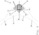
- Figure 4 depicts a second exemplary embodiment of an optical element 10 according to the present invention.
- the distance between adjacent scattering centers SC varies. More specifically, in the exemplary embodiment of Figure 4 , the scattering centers SC form an array of scattering centers SC where the distance between adjacent scattering centers SC decreases from the access ports P1 and P2 towards the array's middle section.
- the array's edges are circularly bent at the access ports P1 and P2 in order to enable mode coupling via shorter adjacent tapers 20.
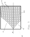
- Figure 5 visualizes section V of Figure 4 and the arrangement of the scattering centers SC in further detail.
- the arrangement of the scattering centers SC in the scattering plane SP is again axially symmetric with respect to the mirror axis M that mirrors the first and second direction D1 and D2 with respect to one another.
- the arrangement of the scattering centers SC is axially asymmetric with respect to the first and/or second direction D1 and D2.
- Figure 6 depicts a third exemplary embodiment of an optical element 10 according to the present invention.
- an access port P11 is connected to a waveguide 11a.
- the access port P11 allows inputting radiation R11 with a first mode.
- the first mode is a TE00-mode.
- a second access side S2 of the optical element 10 provides a first access port P21 and second access port P22.
- Each of the latter ports P21 and P22 outputs radiation R21/R22 that comprises the first mode, e. g. said TE00-mode, and at least a second mode in response to the radiation R11 that is inputted at the first access side S1.
- the second mode is a TE10-mode.
- the ports P21 and P22 are connected to waveguides 10b and 10c.
- the waveguides 10a, 10b, and 10c as well as the scattering centers SC lie in the scattering plane SP.
- the size, orientation and arrangement of scattering centers SC determines the conversion and the conversion ratios of the modes.
- the different sizes of the arrows in Figure 6 indicate that the amplitude of the TE10-mode may be smaller than the amplitude of the TE00-mode at the second access side S2.
- optical elements 10 described above in connection with Figures 1-9 can be fabricated based on 248 nm photolithography, which is significantly cheaper than a 193 nm photolithography or e-beam lithography.
- the scattering centers SC discussed above may be used to minimize the parasitic scattered power at integrated receiver or transmitter interfaces, ensuring an efficient coupling in optical waveguides. Undesired effects such as higher-order modes excitation, PDL and polarization crosstalk may be minimized.
- the exemplary embodiments described above in connection with Figures 1-9 are based on silicon photonic 2D grating couplers used as coupling structures.
- the principle can be used in other coupling structures or on other material platforms as well.
- the examples cope with passive components, but the principle can be applied to active elements as well.
- the major advantage of the proposed use of scattering centers compared to other solutions is the reduced fabrication complexity regarding the required minimum features dimensions. With this, even low-resolution lithographic techniques such as 248 nm deep UV lithography can be used for the fabrication, which allows for large-scale cost-effective fabrication.
Landscapes
- Physics & Mathematics (AREA)
- General Physics & Mathematics (AREA)
- Optics & Photonics (AREA)
- Engineering & Computer Science (AREA)
- Microelectronics & Electronic Packaging (AREA)
- Optical Integrated Circuits (AREA)
Claims (15)
- Optisches Element (10) mit einer Vielzahl von Streuzentren (SC), die in einer Streuebene (SP) des optischen Elements (10) angeordnet sind,
wobei- das optische Element (10) mindestens zwei orientierte Gruppen (G1, G2) von orientierten Streuzentren (SC) umfasst,- wobei jeder orientierten Gruppe (G1, G2) eine gruppenindividuelle Orientierung (O1, O2) zugeordnet ist,- wobei die Streuzentren (SC) jeder orientierten Gruppe (G1, G2) in Übereinstimmung mit derselben gruppenindividuellen Orientierung (O1, O2) orientiert sind, und- wobei die gruppenindividuellen Orientierungen (O1, O2) relativ zueinander gewinkelt sinddadurch gekennzeichnet, dass
die Streuzentren (SC) ein Muster von sich wiederholenden Zellen definieren, wobei jede Zelle ein Streuzentrum (SC) aus jeder der orientierten Gruppen (G1, G2) umfasst. - Optisches Element (10) nach Anspruch 1,
dadurch gekennzeichnet, dass
der Winkel zwischen benachbarten gruppenindividuellen Orientierungen (O1, O2) 180° geteilt durch die Anzahl der gruppenindividuellen Orientierungen (O1, O2) entspricht. - Optisches Element (10) nach einem der vorhergehenden Ansprüche,
dadurch gekennzeichnet, dass- eine erste Zugangsseite (S1) des optischen Elements (10) einen erste Zugangsanschluss (P1) zum Einspeisen und/oder Ausgeben von Strahlung (R1) entlang einer ersten Richtung (D1), die in der Streuebene (SP) liegt, und einen zweiten Zugangsanschluss (P2) zum Einspeisen und/oder Ausgeben von Strahlung (R2) entlang einer zweiten Richtung (D2), die sich von der ersten Richtung (D1) unterscheidet und ebenfalls in der Streuebene (SP) liegt, aufweist,- wobei die Anordnung der Streuzentren (SC) in der Streuebene (SP) axialsymmetrisch in Bezug auf die erste und zweite Richtung (D1, D2) ist. - Optisches Element (10) nach einem der vorhergehenden Ansprüche,
dadurch gekennzeichnet, dass- das optische Element (10) einen ersten Zugangsanschluss (P1) zum Einspeisen und/oder Ausgeben von Strahlung (R1) entlang einer ersten Richtung (D1), die in der Streuebene (SP) liegt, und einen zweiten Zugangsanschluss (P2) zum Einspeisen und/oder Ausgeben von Strahlung (R2) entlang einer zweiten Richtung (D2) umfasst, die um einen Winkel zwischen 80° und 90° zur ersten Richtung (D1) abgewinkelt ist und ebenfalls in der Streuebene (SP) liegt,- wobei die Anordnung der Streuzentren (SC) in der Streuebene (SP) axialsymmetrisch in Bezug auf eine Spiegelachse ist, die die erste und zweite Richtung (D1, D2) zueinander spiegelt. - Optisches Element (10) nach einem der vorhergehenden Ansprüche,
dadurch gekennzeichnet, dass
die Streuzentren (SC) ein Array von Streuzentren (SC) bilden, wobei der Abstand zwischen benachbarten Streuzentren (SC) von der Mitte des Arrays zum Rand des Arrays hin zunimmt. - Optisches Element (10) nach einem der vorhergehenden Ansprüche,
dadurch gekennzeichnet, dass
alle Streuzentren (SC), die zur gleichen Gruppe (G1, G2) gehören, die gleiche Form und/oder Größe haben. - Optisches Element (10) nach einem der vorhergehenden Ansprüche,
dadurch gekennzeichnet, dass
die Streuzentren (SC) der orientierten Gruppen (G1, G2) rotationsasymmetrisch sind. - Optisches Element (10) nach einem der vorhergehenden Ansprüche,
dadurch gekennzeichnet, dass
die Streuzentren (SC) der orientierten Gruppen achsensymmetrisch in Bezug auf die gruppenindividuelle Orientierung (O1, O2) ihrer Gruppe (G1, G2) sind. - Optisches Element (10) nach einem der vorhergehenden Ansprüche,
dadurch gekennzeichnet, dass
alle Streuzentren der orientierten Gruppen die gleiche Form und/oder die gleiche Größe haben. - Optisches Element (10) nach einem der vorhergehenden Ansprüche,
dadurch gekennzeichnet, dass
die Streuzentren (SC) der orientierten Gruppen entlang der jeweiligen gruppenindividuellen Orientierung (O1, O2) gestreckt sind. - Optisches Element (10) nach einem der vorhergehenden Ansprüche,
dadurch gekennzeichnet, dass
das optische Element (10) außerdem mindestens eine nicht orientierte Gruppe (G3) von nicht orientierten Streuzentren (SC) umfasst. - Optisches Element (10) nach einem der vorhergehenden Ansprüche,
dadurch gekennzeichnet, dass
das optische Element (10) mindestens eine Gruppe (G3) von kreisförmigen Streuzentren (SC) umfasst. - Optisches Element (10) nach einem der vorhergehenden Ansprüche,
dadurch gekennzeichnet, dass- das optische Element (10) eine erste Gruppe (G1) von Streuzentren (SC) und eine zweite Gruppe (G2) von Streuzentren (SC) umfasst,- wobei die Streuzentren (SC) der ersten Gruppe (G1) entlang einer ersten Orientierung (O1) orientiert sind,- wobei die Streuzentren (SC) der zweiten Gruppe (G2) entlang einer zweiten Orientierung (O2) orientiert sind, und- wobei die erste Orientierung (O1) und die zweite Orientierung (O2) um 90° abgewinkelt sind. - Optisches Element (10) nach einem der vorhergehenden Ansprüche,
dadurch gekennzeichnet, dass- eine erste Zugangsseite (S1) des optischen Elements (10) einen Zugangsanschluss(P11) zur Einspeisung von Strahlung (R11) mit einer ersten Mode bereitstellt, und- eine zweite Zugangsseite (S2) des optischen Elements (10) einen ersten und einen zweiten Zugangsanschluss (P21, P22) bereitstellt, von denen jeder als Reaktion auf die Strahlung (R11), die an der ersten Zugangsseite (S1) eingespeist wird, Strahlung (R21, R22) mit der ersten Mode und mindestens einer zweiten Mode ausgibt. - Optisches Element (10) nach einem der vorhergehenden Ansprüche,
dadurch gekennzeichnet, dass- das optische Element (10) ein Polarisations-Multiplexer/Demultiplexer ist,- wobei das optische Element (10) einen ersten Zugangsanschluss (P1) zum Einspeisen und/oder Ausgeben von Strahlung (R1) mit einer ersten Polarisation und einen zweiten Zugangsanschluss (P2) zum Einspeisen und/oder Ausgeben von Strahlung (R2) mit einer zweiten Polarisation, die sich von der ersten Polarisation unterscheidet, bereitstellt, und- wobei das optische Element (10) einen dritten Zugangsanschluss (P3) zum Einspeisen und/oder Ausgeben von Strahlung (R3) bereitstellt, die sowohl die erste als auch die zweite Polarisation aufweist.
Priority Applications (2)
| Application Number | Priority Date | Filing Date | Title |
|---|---|---|---|
| EP21194821.1A EP4145200B1 (de) | 2021-09-03 | 2021-09-03 | Optisches element |
| US17/902,023 US20230085272A1 (en) | 2021-09-03 | 2022-09-02 | Optical element |
Applications Claiming Priority (1)
| Application Number | Priority Date | Filing Date | Title |
|---|---|---|---|
| EP21194821.1A EP4145200B1 (de) | 2021-09-03 | 2021-09-03 | Optisches element |
Publications (3)
| Publication Number | Publication Date |
|---|---|
| EP4145200A1 EP4145200A1 (de) | 2023-03-08 |
| EP4145200B1 true EP4145200B1 (de) | 2025-05-28 |
| EP4145200C0 EP4145200C0 (de) | 2025-05-28 |
Family
ID=77640464
Family Applications (1)
| Application Number | Title | Priority Date | Filing Date |
|---|---|---|---|
| EP21194821.1A Active EP4145200B1 (de) | 2021-09-03 | 2021-09-03 | Optisches element |
Country Status (2)
| Country | Link |
|---|---|
| US (1) | US20230085272A1 (de) |
| EP (1) | EP4145200B1 (de) |
Family Cites Families (14)
| Publication number | Priority date | Publication date | Assignee | Title |
|---|---|---|---|---|
| JP4336008B2 (ja) * | 1998-11-17 | 2009-09-30 | 日本発條株式会社 | 対象物の識別構造及び識別方法 |
| US6829417B2 (en) * | 2001-08-27 | 2004-12-07 | Christoph M. Greiner | Amplitude and phase control in distributed optical structures |
| US7006732B2 (en) * | 2003-03-21 | 2006-02-28 | Luxtera, Inc. | Polarization splitting grating couplers |
| JP4410123B2 (ja) * | 2005-02-10 | 2010-02-03 | 株式会社東芝 | 有機elディスプレイ |
| TW200903465A (en) * | 2007-07-03 | 2009-01-16 | Ind Tech Res Inst | Difrraction grating recording medium |
| US8619363B1 (en) * | 2007-11-06 | 2013-12-31 | Fusion Optix, Inc. | Light redirecting element comprising a forward diffracting region and a scattering region |
| US8676003B2 (en) * | 2009-10-28 | 2014-03-18 | Universiteit Gent | Methods and systems for reducing polarization dependent loss |
| US8660391B1 (en) * | 2011-09-30 | 2014-02-25 | Aurrion, Inc. | Heterogeneous waveguide integrated optical isolator and circulator utilizing one or more optical grating couplers |
| JP2017527857A (ja) * | 2014-09-15 | 2017-09-21 | カリフォルニア インスティチュート オブ テクノロジー | 平面デバイスを用いた偏光および波面の同時制御 |
| US20160337041A1 (en) * | 2015-05-15 | 2016-11-17 | Futurewei Technologies, Inc. | Polarization Independent Reflective Modulator |
| US20170153391A1 (en) * | 2015-11-30 | 2017-06-01 | Google Inc. | Photonic chip optical transceivers |
| JP7062366B2 (ja) * | 2017-03-03 | 2022-05-06 | 株式会社ジャパンディスプレイ | 表示装置、表示方法及び色分離素子 |
| CN110770615A (zh) * | 2017-04-19 | 2020-02-07 | 卢克斯特拉有限公司 | 用于二维模式匹配光栅耦合器的方法和系统 |
| CN111192978B (zh) * | 2020-02-26 | 2022-08-09 | 武汉天马微电子有限公司 | 显示面板和显示装置 |
-
2021
- 2021-09-03 EP EP21194821.1A patent/EP4145200B1/de active Active
-
2022
- 2022-09-02 US US17/902,023 patent/US20230085272A1/en active Pending
Also Published As
| Publication number | Publication date |
|---|---|
| US20230085272A1 (en) | 2023-03-16 |
| EP4145200A1 (de) | 2023-03-08 |
| EP4145200C0 (de) | 2025-05-28 |
Similar Documents
| Publication | Publication Date | Title |
|---|---|---|
| EP1606660B1 (de) | Gitterkoppler zur polarisationsteilung | |
| US20220019020A1 (en) | Method and Apparatus for Optical Waveguide-to-Semiconductor Coupling for Integrated Photonic Circuits | |
| WO2013160902A1 (en) | System and method for mode division multiplexing | |
| JP2010524022A (ja) | マルチプレクサ導波路結合方法およびシステム | |
| CN115244441B (zh) | 用于光纤通信的使用超材料的模态复用器/解复用器 | |
| CN106936708A (zh) | NxN波长路由网络拓扑、光子集成芯片及光路由器 | |
| CN117242716B (zh) | 光学收发器、连接到该光学收发器的交换机和系统 | |
| WO2016002922A1 (ja) | 空間-oam変換・oam合分岐デバイス、oam伝送システム及びoam-admネットワークシステム | |
| EP4145200B1 (de) | Optisches element | |
| US20120251105A1 (en) | Method and apparatus for providing a line of spots launch of light into an end of a multimode optical fiber | |
| CN115349102B (zh) | 用于光学通信系统及光学通信的使用超材料的模式多路复用器/解复用器 | |
| Lataoui et al. | Multicore raised cosine fibers for next generation space division multiplexing systems | |
| Khulbe et al. | Orbital angular momentum wave generation and multiplexing: Experiments and analysis using classical and quantum optics | |
| CN106569329A (zh) | 一种模式和空间光交换的方法和装置 | |
| Feng et al. | Photonics breakthroughs 2024: multidimensional integrated (de) multiplexers for optical fiber communications | |
| WO2020162216A1 (ja) | インタポーザ回路 | |
| Yin et al. | Scalable 3D silicon optical switch based on CLOS architecture | |
| CN116224475B (zh) | 光转换器及光转换系统 | |
| US12498522B2 (en) | Compact dual polarization couplers for multi-core optical fibers | |
| Sobu et al. | Demonstration of low polarization dependent loss of 1.3 μm two dimensional grating coupler | |
| US20040179780A1 (en) | Optical coupler with low loss interconnections | |
| CN115951452B (zh) | 一种基于多相位面的多模波导耦合器 | |
| Yan et al. | Inverse Design of Ultra-Compact Interlayer Couplers for High-Efficiency Silicon-Based Optical Signal Transmission | |
| US20240151963A1 (en) | Optical phased array device that can flexibly set the light splitting weight and has good scalability | |
| SeyedinNavadeh et al. | Photonics Breakthroughs 2024: Arbitrary Mode Manipulation Using Reconfigurable Integrated Photonic Processors |
Legal Events
| Date | Code | Title | Description |
|---|---|---|---|
| PUAI | Public reference made under article 153(3) epc to a published international application that has entered the european phase |
Free format text: ORIGINAL CODE: 0009012 |
|
| STAA | Information on the status of an ep patent application or granted ep patent |
Free format text: STATUS: THE APPLICATION HAS BEEN PUBLISHED |
|
| AK | Designated contracting states |
Kind code of ref document: A1 Designated state(s): AL AT BE BG CH CY CZ DE DK EE ES FI FR GB GR HR HU IE IS IT LI LT LU LV MC MK MT NL NO PL PT RO RS SE SI SK SM TR |
|
| STAA | Information on the status of an ep patent application or granted ep patent |
Free format text: STATUS: REQUEST FOR EXAMINATION WAS MADE |
|
| 17P | Request for examination filed |
Effective date: 20230828 |
|
| RBV | Designated contracting states (corrected) |
Designated state(s): AL AT BE BG CH CY CZ DE DK EE ES FI FR GB GR HR HU IE IS IT LI LT LU LV MC MK MT NL NO PL PT RO RS SE SI SK SM TR |
|
| STAA | Information on the status of an ep patent application or granted ep patent |
Free format text: STATUS: EXAMINATION IS IN PROGRESS |
|
| 17Q | First examination report despatched |
Effective date: 20231013 |
|
| RAP1 | Party data changed (applicant data changed or rights of an application transferred) |
Owner name: DR. GEORGIEVA, GALINA |
|
| RIN1 | Information on inventor provided before grant (corrected) |
Inventor name: DR. GEORGIEVA, GALINA |
|
| GRAP | Despatch of communication of intention to grant a patent |
Free format text: ORIGINAL CODE: EPIDOSNIGR1 |
|
| STAA | Information on the status of an ep patent application or granted ep patent |
Free format text: STATUS: GRANT OF PATENT IS INTENDED |
|
| INTG | Intention to grant announced |
Effective date: 20240925 |
|
| GRAJ | Information related to disapproval of communication of intention to grant by the applicant or resumption of examination proceedings by the epo deleted |
Free format text: ORIGINAL CODE: EPIDOSDIGR1 |
|
| STAA | Information on the status of an ep patent application or granted ep patent |
Free format text: STATUS: EXAMINATION IS IN PROGRESS |
|
| GRAP | Despatch of communication of intention to grant a patent |
Free format text: ORIGINAL CODE: EPIDOSNIGR1 |
|
| STAA | Information on the status of an ep patent application or granted ep patent |
Free format text: STATUS: GRANT OF PATENT IS INTENDED |
|
| INTC | Intention to grant announced (deleted) | ||
| INTG | Intention to grant announced |
Effective date: 20241219 |
|
| GRAS | Grant fee paid |
Free format text: ORIGINAL CODE: EPIDOSNIGR3 |
|
| GRAA | (expected) grant |
Free format text: ORIGINAL CODE: 0009210 |
|
| STAA | Information on the status of an ep patent application or granted ep patent |
Free format text: STATUS: THE PATENT HAS BEEN GRANTED |
|
| AK | Designated contracting states |
Kind code of ref document: B1 Designated state(s): AL AT BE BG CH CY CZ DE DK EE ES FI FR GB GR HR HU IE IS IT LI LT LU LV MC MK MT NL NO PL PT RO RS SE SI SK SM TR |
|
| REG | Reference to a national code |
Ref country code: GB Ref legal event code: FG4D |
|
| REG | Reference to a national code |
Ref country code: CH Ref legal event code: EP |
|
| REG | Reference to a national code |
Ref country code: IE Ref legal event code: FG4D Ref country code: DE Ref legal event code: R096 Ref document number: 602021031366 Country of ref document: DE |
|
| U01 | Request for unitary effect filed |
Effective date: 20250626 |
|
| U07 | Unitary effect registered |
Designated state(s): AT BE BG DE DK EE FI FR IT LT LU LV MT NL PT RO SE SI Effective date: 20250702 |
|
| U20 | Renewal fee for the european patent with unitary effect paid |
Year of fee payment: 5 Effective date: 20250826 |
|
| PG25 | Lapsed in a contracting state [announced via postgrant information from national office to epo] |
Ref country code: ES Free format text: LAPSE BECAUSE OF FAILURE TO SUBMIT A TRANSLATION OF THE DESCRIPTION OR TO PAY THE FEE WITHIN THE PRESCRIBED TIME-LIMIT Effective date: 20250528 |
|
| PG25 | Lapsed in a contracting state [announced via postgrant information from national office to epo] |
Ref country code: NO Free format text: LAPSE BECAUSE OF FAILURE TO SUBMIT A TRANSLATION OF THE DESCRIPTION OR TO PAY THE FEE WITHIN THE PRESCRIBED TIME-LIMIT Effective date: 20250828 Ref country code: GR Free format text: LAPSE BECAUSE OF FAILURE TO SUBMIT A TRANSLATION OF THE DESCRIPTION OR TO PAY THE FEE WITHIN THE PRESCRIBED TIME-LIMIT Effective date: 20250829 |
|
| PG25 | Lapsed in a contracting state [announced via postgrant information from national office to epo] |
Ref country code: PL Free format text: LAPSE BECAUSE OF FAILURE TO SUBMIT A TRANSLATION OF THE DESCRIPTION OR TO PAY THE FEE WITHIN THE PRESCRIBED TIME-LIMIT Effective date: 20250528 |
|
| PG25 | Lapsed in a contracting state [announced via postgrant information from national office to epo] |
Ref country code: HR Free format text: LAPSE BECAUSE OF FAILURE TO SUBMIT A TRANSLATION OF THE DESCRIPTION OR TO PAY THE FEE WITHIN THE PRESCRIBED TIME-LIMIT Effective date: 20250528 |
|
| PG25 | Lapsed in a contracting state [announced via postgrant information from national office to epo] |
Ref country code: RS Free format text: LAPSE BECAUSE OF FAILURE TO SUBMIT A TRANSLATION OF THE DESCRIPTION OR TO PAY THE FEE WITHIN THE PRESCRIBED TIME-LIMIT Effective date: 20250828 |
|
| PG25 | Lapsed in a contracting state [announced via postgrant information from national office to epo] |
Ref country code: IS Free format text: LAPSE BECAUSE OF FAILURE TO SUBMIT A TRANSLATION OF THE DESCRIPTION OR TO PAY THE FEE WITHIN THE PRESCRIBED TIME-LIMIT Effective date: 20250928 |
|
| PG25 | Lapsed in a contracting state [announced via postgrant information from national office to epo] |
Ref country code: SM Free format text: LAPSE BECAUSE OF FAILURE TO SUBMIT A TRANSLATION OF THE DESCRIPTION OR TO PAY THE FEE WITHIN THE PRESCRIBED TIME-LIMIT Effective date: 20250528 |
|
| PG25 | Lapsed in a contracting state [announced via postgrant information from national office to epo] |
Ref country code: CZ Free format text: LAPSE BECAUSE OF FAILURE TO SUBMIT A TRANSLATION OF THE DESCRIPTION OR TO PAY THE FEE WITHIN THE PRESCRIBED TIME-LIMIT Effective date: 20250528 |
|
| PG25 | Lapsed in a contracting state [announced via postgrant information from national office to epo] |
Ref country code: SK Free format text: LAPSE BECAUSE OF FAILURE TO SUBMIT A TRANSLATION OF THE DESCRIPTION OR TO PAY THE FEE WITHIN THE PRESCRIBED TIME-LIMIT Effective date: 20250528 |