EP4145183A1 - Radiation detector and radiation detection device - Google Patents
Radiation detector and radiation detection device Download PDFInfo
- Publication number
- EP4145183A1 EP4145183A1 EP22795455.9A EP22795455A EP4145183A1 EP 4145183 A1 EP4145183 A1 EP 4145183A1 EP 22795455 A EP22795455 A EP 22795455A EP 4145183 A1 EP4145183 A1 EP 4145183A1
- Authority
- EP
- European Patent Office
- Prior art keywords
- radiation
- closed space
- radiation detector
- radiation detection
- detection element
- Prior art date
- Legal status (The legal status is an assumption and is not a legal conclusion. Google has not performed a legal analysis and makes no representation as to the accuracy of the status listed.)
- Pending
Links
Images






Classifications
-
- G—PHYSICS
- G01—MEASURING; TESTING
- G01T—MEASUREMENT OF NUCLEAR OR X-RADIATION
- G01T7/00—Details of radiation-measuring instruments
-
- G—PHYSICS
- G01—MEASURING; TESTING
- G01T—MEASUREMENT OF NUCLEAR OR X-RADIATION
- G01T1/00—Measuring X-radiation, gamma radiation, corpuscular radiation, or cosmic radiation
- G01T1/16—Measuring radiation intensity
- G01T1/24—Measuring radiation intensity with semiconductor detectors
- G01T1/244—Auxiliary details, e.g. casings, cooling, damping or insulation against damage by, e.g. heat, pressure or the like
-
- G—PHYSICS
- G01—MEASURING; TESTING
- G01N—INVESTIGATING OR ANALYSING MATERIALS BY DETERMINING THEIR CHEMICAL OR PHYSICAL PROPERTIES
- G01N2223/00—Investigating materials by wave or particle radiation
- G01N2223/07—Investigating materials by wave or particle radiation secondary emission
- G01N2223/076—X-ray fluorescence
-
- G—PHYSICS
- G01—MEASURING; TESTING
- G01N—INVESTIGATING OR ANALYSING MATERIALS BY DETERMINING THEIR CHEMICAL OR PHYSICAL PROPERTIES
- G01N2223/00—Investigating materials by wave or particle radiation
- G01N2223/07—Investigating materials by wave or particle radiation secondary emission
- G01N2223/079—Investigating materials by wave or particle radiation secondary emission incident electron beam and measuring excited X-rays
-
- G—PHYSICS
- G01—MEASURING; TESTING
- G01N—INVESTIGATING OR ANALYSING MATERIALS BY DETERMINING THEIR CHEMICAL OR PHYSICAL PROPERTIES
- G01N2223/00—Investigating materials by wave or particle radiation
- G01N2223/50—Detectors
- G01N2223/507—Detectors secondary-emission detector
-
- G—PHYSICS
- G01—MEASURING; TESTING
- G01N—INVESTIGATING OR ANALYSING MATERIALS BY DETERMINING THEIR CHEMICAL OR PHYSICAL PROPERTIES
- G01N23/00—Investigating or analysing materials by the use of wave or particle radiation, e.g. X-rays or neutrons, not covered by groups G01N3/00 – G01N17/00, G01N21/00 or G01N22/00
- G01N23/22—Investigating or analysing materials by the use of wave or particle radiation, e.g. X-rays or neutrons, not covered by groups G01N3/00 – G01N17/00, G01N21/00 or G01N22/00 by measuring secondary emission from the material
- G01N23/223—Investigating or analysing materials by the use of wave or particle radiation, e.g. X-rays or neutrons, not covered by groups G01N3/00 – G01N17/00, G01N21/00 or G01N22/00 by measuring secondary emission from the material by irradiating the sample with X-rays or gamma-rays and by measuring X-ray fluorescence
-
- G—PHYSICS
- G01—MEASURING; TESTING
- G01N—INVESTIGATING OR ANALYSING MATERIALS BY DETERMINING THEIR CHEMICAL OR PHYSICAL PROPERTIES
- G01N23/00—Investigating or analysing materials by the use of wave or particle radiation, e.g. X-rays or neutrons, not covered by groups G01N3/00 – G01N17/00, G01N21/00 or G01N22/00
- G01N23/22—Investigating or analysing materials by the use of wave or particle radiation, e.g. X-rays or neutrons, not covered by groups G01N3/00 – G01N17/00, G01N21/00 or G01N22/00 by measuring secondary emission from the material
- G01N23/225—Investigating or analysing materials by the use of wave or particle radiation, e.g. X-rays or neutrons, not covered by groups G01N3/00 – G01N17/00, G01N21/00 or G01N22/00 by measuring secondary emission from the material using electron or ion
- G01N23/2251—Investigating or analysing materials by the use of wave or particle radiation, e.g. X-rays or neutrons, not covered by groups G01N3/00 – G01N17/00, G01N21/00 or G01N22/00 by measuring secondary emission from the material using electron or ion using incident electron beams, e.g. scanning electron microscopy [SEM]
- G01N23/2252—Measuring emitted X-rays, e.g. electron probe microanalysis [EPMA]
Definitions
- the present invention relates to a radiation detector and a radiation detection apparatus.
- a radiation detector detecting radiation such as X-rays may include a radiation detection element using a semiconductor.
- the radiation detector is provided with a circuit element such as a preamplifier amplifying a signal output by the radiation detection element.
- the radiation detector includes a housing, and the radiation detection element and the circuit element are disposed inside the housing.
- a substrate is disposed inside the housing, the radiation detection element is provided on the surface of the substrate, and the circuit element is provided on the back surface of the substrate.
- the housing is provided with a window having a window material formed of a radiation-transmitting material. Radiation transmitted through the window material is detected. Radiation that cannot be transmitted through the window material due to the low energy thereof cannot be detected by the radiation detector.
- Patent Document 1 discloses an example of a window material-less radiation detector.
- Patent Document 1 International Publication No. WO2019/117272
- a gas such as water vapor enters from the outside to the inside of the radiation detector. Gas adsorption to a circuit element in the radiation detector may occur to cause circuit element deterioration and degradation in the performance of the radiation detector.
- the present invention has been made in view of such circumstances, and an object of the present invention is to provide a radiation detector and a radiation detection apparatus capable of suppressing degradation in performance.
- a radiation detector includes a radiation detection element, a circuit element, and a housing accommodating the radiation detection element and the circuit element, is characterized in that a closed space is provided, the housing has an unblocked opening portion, the closed space is disposed inside the housing, the circuit element is disposed in the closed space, and the closed space is decompressed or filled with an inert gas or a dry gas.
- the housing of the radiation detector has the unblocked opening portion.
- the radiation detector includes the closed space, and the circuit element such as an amplifier is disposed in the closed space.
- a gas such as water vapor is capable of entering the inside of the housing through the opening portion but does not enter the closed space. Accordingly, even in a case where the radiation detector is used in a normal-pressure or low-vacuum environment, the gas that has entered from the outside is not adsorbed to the circuit element.
- the inside of the closed space is decompressed or filled with an inert or dry gas.
- the radiation detection element is disposed at a position facing the opening portion.
- the radiation detection element faces the opening portion.
- the radiation incident on the radiation detection element passes through the opening portion and does not have to be transmitted through a window material. Accordingly, the radiation detector is capable of detecting radiation that cannot be transmitted through a window material due to the low energy thereof.
- a radiation detector includes a radiation detection element having an incident surface where radiation is incident and a circuit element, is characterized in that a closed space disposed at a position not facing the incident surface is provided, the circuit element is disposed in the closed space, and the closed space is decompressed or filled with an inert gas or a dry gas.
- the radiation detector includes the closed space and the circuit element such as an amplifier is disposed in the closed space.
- the incident surface of the radiation detection element does not face the closed space.
- a gas such as water vapor does not enter the closed space. Accordingly, gas adsorption to the circuit element does not occur.
- the inside of the closed space is decompressed or filled with an inert or dry gas. Water or gas adsorption to the circuit element is unlikely to occur, and deterioration of the circuit element attributable to water or gas adsorption is prevented.
- the radiation detection element has an electrode connected to the circuit element, and the electrode faces the closed space.
- the radiation detection element includes the electrode for connection to the circuit element and the electrode faces the closed space.
- the radiation detector according to the present invention is characterized by further comprising a moisture getter taking in moisture in the closed space.
- the moisture getter takes in the moisture in the closed space. Accordingly, water adsorption to the circuit element is more effectively prevented.
- the radiation detector according to the present invention is characterized by further comprising a gas getter taking in a gas in the closed space.
- the gas getter takes in the gas in the closed space. Accordingly, gas adsorption to the circuit element is more effectively prevented.
- the radiation detector according to the present invention is characterized by further comprising: a substrate having a first surface and a second surface positioned behind the first surface; and a plate-shaped member, wherein the substrate has a through hole penetrating the substrate between the first surface and the second surface, the radiation detection element is disposed on the first surface and blocks one end of the through hole, the plate-shaped member is disposed so as to face the second surface and blocks the other end of the through hole, and the closed space is a space in the through hole blocked at both ends by the radiation detection element and the plate-shaped member.
- the radiation detector includes the substrate having the through hole, the radiation detection element is disposed so as to block one end of the through hole, and the plate-shaped member is disposed so as to block the other end of the through hole.
- the space in the through hole is to be the closed space by the radiation detection element and the plate-shaped member blocking both ends of the through hole. The closed space where no gas enters is configured with ease.
- the radiation detector according to the present invention is characterized by further comprising: a substrate having a first surface and a second surface positioned behind the first surface; and a plate-shaped member having a cavity inside, wherein the substrate has a through hole penetrating the substrate between the first surface and the second surface, the radiation detection element is disposed on the first surface and blocks one end of the through hole, the plate-shaped member is disposed so as to face the second surface and blocks the other end of the through hole, the plate-shaped member has a connecting hole smaller in diameter than the through hole and connecting a space in the through hole and the cavity, at a part facing the second surface, the closed space includes the space in the through hole blocked at both ends by the radiation detection element and the plate-shaped member and the cavity connected to the space via the connecting hole, and a moisture getter taking in moisture in the closed space or a gas getter taking in a gas in the closed space is disposed at a position in the cavity different from the connecting hole.
- the radiation detector includes the substrate having the through hole, the radiation detection element is disposed so as to block one end of the through hole, and the plate-shaped member is disposed so as to block the other end of the through hole.
- the plate-shaped member has the cavity inside and has the connecting hole connecting the space in the through hole and the cavity.
- the closed space including the space in the through hole and the cavity connected to the space via the connecting hole is configured.
- the moisture getter or the gas getter is disposed at the position in the cavity different from the connecting hole.
- a part of a shield plate is between the moisture getter or the gas getter and the radiation detection element, and characteristic X-rays from the moisture getter or the gas getter are shielded by the shield plate. Accordingly, a system peak attributable to the moisture getter or the gas getter is unlikely to occur.
- the radiation detector according to the present invention is characterized by further comprising a cooling unit for cooling the radiation detection element.
- the radiation detector includes the cooling unit such as a Peltier element for cooling the radiation detection element.
- the cooling of the radiation detection element leads to noise reduction and radiation detection accuracy improvement. Even with the radiation detection element cooled, adsorption of a gas such as water vapor to the circuit element is prevented.
- the circuit element configures at least a part of an amplifier circuit amplifying a signal output by the radiation detection element.
- the circuit element configures at least a part of the amplifier circuit. Deterioration of the amplifier circuit is prevented, and thus deterioration of the signal output from the radiation detector is prevented and degradation in radiation detection accuracy is suppressed.
- a radiation detection apparatus is characterized by comprising: the radiation detector according to the present invention; and a spectrum generation unit generating a spectrum of radiation detected by the radiation detector.
- a radiation detection apparatus is characterized by comprising: an irradiation unit irradiating a sample with radiation; the radiation detector according to the present invention detecting radiation generated from the sample; a spectrum generation unit generating a spectrum of the radiation detected by the radiation detector; and a display unit displaying the spectrum generated by the spectrum generation unit.
- deterioration of the circuit element attributable to gas adsorption to the circuit element of the radiation detector is prevented. Accordingly, degradation in the performance of the radiation detector is suppressed. In particular, even in a case where the window material-less radiation detector is used in a normal-pressure or low-vacuum environment, degradation in the performance of the radiation detector is suppressed.
- FIG. 1 is a schematic perspective view illustrating an example of the appearance of a radiation detector 1 according to Embodiment 1.
- FIG. 2 is a schematic cross-sectional view illustrating a configuration example of the radiation detector 1 according to Embodiment 1.
- FIG. 3 is a block diagram illustrating a functional configuration example of a radiation detection apparatus 10.
- the radiation detection apparatus 10 is, for example, a fluorescent X-ray analyzer.
- the radiation detection apparatus 10 includes an irradiation unit 4 irradiating a sample 6 with radiation such as electron beams or X-rays, a sample table 5 where the sample 6 is placed, and the radiation detector 1. Radiation is emitted from the irradiation unit 4 to the sample 6, radiation such as fluorescent X-rays is generated at the sample 6, and the radiation detector 1 detects the radiation generated from the sample 6. In the drawing, the radiation is indicated by arrows.
- the radiation detector 1 outputs a signal proportional to the energy of the detected radiation. It should be noted that the radiation detection apparatus 10 in another form may hold the sample 6 by a method other than placement on the sample table 5.
- a signal processing unit 2 processing the output signal and a voltage application unit 34 applying a voltage necessary for radiation detection to a radiation detection element 11 of the radiation detector 1.
- the signal processing unit 2 detects a signal value corresponding to the energy of the radiation detected by the radiation detector 1 by detecting the wave height of the pulse signal output by the radiation detector 1.
- An analysis unit 32 is connected to the signal processing unit 2.
- the analysis unit 32 is configured to include a calculation unit performing calculation and a memory storing data.
- the signal processing unit 2, the analysis unit 32, the voltage application unit 34, and the irradiation unit 4 are connected to a control unit 31.
- the control unit 31 controls the operations of the signal processing unit 2, the analysis unit 32, the voltage application unit 34, and the irradiation unit 4.
- the signal processing unit 2 outputs data indicating the detected signal value to the analysis unit 32.
- the analysis unit 32 counts the signal of each value and performs processing to generate the relationship between the energy of the radiation and the count number, that is, the spectrum of the radiation.
- the signal processing unit 2 and the analysis unit 32 correspond to a spectrum generation unit.
- the analysis unit 32 performs qualitative analysis or quantitative analysis of elements contained in the sample 6 based on the spectrum. It should be noted that the signal processing unit 2 may generate the radiation spectrum.
- a display unit 33 such as a liquid crystal display is connected to the analysis unit 32.
- the display unit 33 displays the spectrum generated by the analysis unit 32 and the analysis result by the analysis unit 32.
- the control unit 31 may be configured to receive a user operation and control each unit of the radiation detection apparatus 10 in accordance with the received operation.
- the control unit 31 and the analysis unit 32 may be configured by the same computer.
- the radiation detector 1 includes a plate-shaped bottom plate portion 18.
- One surface side of the bottom plate portion 18 is covered with a cap-shaped cover 13.
- the cover 13 has a shape in which a truncated cone is connected to one end of a cylinder, and the other end of the cylinder is joined to the bottom plate portion 18.
- An opening portion 131 is formed at the truncated part of the tip of the cover 13.
- a window having a window material is not provided in the opening portion 131, and the opening portion 131 is blocked by no window materials.
- the cover 13 and the bottom plate portion 18 configure the housing of the radiation detector 1.
- the cover 13 and the bottom plate portion 18 accommodate other parts of the radiation detector 1. Gas can be exchanged between the inside and outside of the cover 13 and the bottom plate portion 18.
- the radiation detection element 11, a collimator 12, a substrate 14, a shield plate 16, a Peltier element 17, and a cold finger 172 are disposed inside the cover 13.
- the substrate 14 has a first surface 141 facing the opening portion 131, and the radiation detection element 11 is disposed on the first surface 141.
- An interposed object such as an adhesive may be present between the substrate 14 and the radiation detection element 11.
- the substrate 14 is desirably formed of a material that generates as little radiation as possible when irradiated with radiation.
- the material of the substrate 14 is, for example, ceramic.
- the radiation detection element 11 is a silicon drift-type radiation detection element, and the radiation detector 1 is a silicon drift detector (SDD).
- the radiation detection element 11 is plate-shaped.
- the radiation detection element 11 is disposed at a position facing the opening portion 131.
- the radiation detection element 11 has an incident surface 110 where radiation to be detected is incident, and the incident surface 110 is disposed so as to face the opening portion 131.
- the collimator 12 has a tubular shape with both ends open and is made of a radiation shielding material.
- the collimator 12 is disposed between the radiation detection element 11 and the opening portion 131.
- One end of the collimator 12 faces the opening portion 131, and the other end faces the incident surface 110 of the radiation detection element 11.
- An adhesive layer 121 consisting of an insulating adhesive and coating is provided between the collimator 12 and the radiation detection element 11.
- the collimator 12 is attached to the incident surface 110 of the radiation detection element 11 via the adhesive layer 121. Radiation is incident on the inside of the cover 13 mainly through the opening portion 131, the collimator 12 shields part of the radiation, and the radiation detection element 11 detects the radiation not shielded by the collimator 12.
- the substrate 14 has a second surface 142 positioned behind the first surface 141.
- the shield plate 16 is disposed at a position facing the second surface 142.
- the shield plate 16 corresponds to a plate-shaped member.
- the shield plate 16 shields radiation incident from outside the shield plate 16 when viewed from the radiation detection element 11.
- the shield plate 16 is in contact with the second surface 142.
- An interposed object such as an adhesive may be interposed between the shield plate 16 and the second surface 142.
- the Peltier element 17 has a heat-absorbing part that is in thermal contact with the back surface of the shield plate 16 behind the surface of the shield plate 16 in contact with the substrate 14.
- the Peltier element 17 may be in direct contact with the shield plate 16 or a thermally conductive substance may be interposed between the Peltier element 17 and the shield plate 16.
- a waterproof coating material 171 is applied around the part where the Peltier element 17 and the shield plate 16 are in contact with each other.
- the waterproof coating material 171 is, for example, a waterproof resin.
- the waterproof coating material 171 prevents water generated by cooling from entering between the Peltier element 17 and the shield plate 16.
- the Peltier element 17 has a heat-dissipating part that is in thermal contact with the cold finger 172.
- the cold finger 172 is configured to include a flat plate-shaped part with which the heat-dissipating part of the Peltier element 17 is in thermal contact and a bolt-shaped part protruding from the flat plate-shaped part.
- the bolt-shaped part of the cold finger 172 penetrates the bottom plate portion 18 and protrudes from the outer surface of the bottom plate portion 18.
- the Peltier element 17 may be in direct contact with the cold finger 172 or a thermally conductive substance may be interposed between the Peltier element 17 and the cold finger 172.
- the cold finger 172 is formed of a material with high thermal conductivity.
- the bolt-shaped part of the cold finger 172 is connected to a heat-dissipating portion outside the radiation detector 1.
- the heat-dissipating portion is, for example, a heat sink.
- the heat of the radiation detection element 11 is conducted to the heat-absorbing part of the Peltier element 17 through the substrate 14 and the shield plate 16.
- the heat is released from the heat-dissipating part of the Peltier element 17 to the outside of the radiation detector 1 through the cold finger 172. In this manner, the heat of the radiation detection element 11 is released to the outside of the radiation detector 1 and the radiation detection element 11 is cooled.
- the Peltier element 17 corresponds to a cooling unit.
- the shield plate 16 is desirably made of a thermally conductive material higher in thermal conductivity than the substrate 14 such that the heat of the radiation detection element 11 can be efficiently conducted to the Peltier element 17.
- the material of the shield plate 16 is alumina.
- the thermal conductivity of alumina is somewhat high.
- the radiation detector 1 in another form may release heat through the bottom plate portion 18 without including the cold finger 172.
- the substrate 14 is provided with an amplifier 151 as will be described later.
- the amplifier 151 corresponds to a circuit element.
- the amplifier 151 is connected to the radiation detection element 11 via a bonding wire 152.
- the substrate 14 is provided with a circuit.
- the amplifier 151 is connected to the circuit.
- the circuit may include a circuit element other than the amplifier 151.
- the radiation detector 1 further includes a plurality of lead pins 181.
- the lead pin 181 penetrates the bottom plate portion 18.
- One end of the lead pin 181 is connected via a bonding wire to the circuit provided on the substrate 14. Electric power supply and signal input and output with respect to the radiation detection element 11 are performed through the lead pins 181.
- the amplifier 151 configures at least a part of an amplifier circuit amplifying the signal output by the radiation detection element 11.
- the amplifier 151 is a preamplifier.
- the radiation detection element 11 outputs a signal proportional to the energy of the detected radiation, and the output signal is input to the amplifier 151 through the bonding wire 152.
- the amplifier 151 performs signal conversion and amplification.
- the converted and amplified signal is output from the amplifier 151 and output to the outside of the radiation detector 1 through the lead pin 181. In this manner, the radiation detector 1 outputs a signal proportional to the energy of the radiation detected by the radiation detection element 11.
- the output signal is input to the signal processing unit 2.
- the amplifier 151 may have a non-preamplifier function.
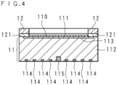
- FIG. 4 is a schematic cross-sectional view illustrating the radiation detection element 11 and the collimator 12.
- a part of the incident surface 110 of the radiation detection element 11 is covered with the collimator 12 and the adhesive layer 121.
- the part that includes the middle part of the incident surface 110 and is not covered with the collimator 12 and the adhesive layer 121 is covered with a light shielding film 111.
- the radiation detection element 11 has a plate-shaped semiconductor portion 112.
- the component of the semiconductor portion 112 is, for example, n-type silicon (Si).
- the incident surface 110 of the radiation detection element 11 is provided with a first electrode 113.
- the first electrode 113 is continuously provided in the region that includes the middle part of the incident surface 110.
- the first electrode 113 is provided up to the vicinity of the peripheral edge of the incident surface 110 and occupies most of the incident surface 110.
- the first electrode 113 is connected to the voltage application unit 34.
- Multiple loop-shaped second electrodes 114 are provided on the back surface of the radiation detection element 11 behind the incident surface 110.
- a signal output electrode 115 outputting a signal during radiation detection is provided at the position surrounded by the multiple second electrodes 114.
- the signal output electrode 115 is connected to the amplifier 151 via the bonding wire 152.
- the second electrode 114 closest to the signal output electrode 115 and the second electrode 114 farthest from the signal output electrode 115 are connected to the voltage application unit 34.
- the voltage application unit 34 performs voltage application to the multiple second electrodes 114 such that the second electrode 114 closest to the signal output electrode 115 has the highest potential and the second electrode 114 farthest from the signal output electrode 115 has the lowest potential.
- the radiation detection element 11 is configured such that a predetermined electrical resistance is generated between the adjacent second electrodes 114. For example, by adjusting the chemical composition of a part of the semiconductor portion 112 positioned between the adjacent second electrodes 114, an electrically resistive channel to which two second electrodes 114 are connected is formed. In other words, the multiple second electrodes 114 are connected in a daisy chain via electrical resistance.
- the respective second electrodes 114 By applying a voltage from the voltage application unit 34 to the multiple second electrodes 114, the respective second electrodes 114 have potentials that monotonically increase in order from the second electrode 114 far from the signal output electrode 115 toward the second electrode 114 close to the signal output electrode 115. It should be noted that the plurality of second electrodes 114 may include a pair of adjacent second electrodes 114 with the same potential.
- the potentials of the plurality of second electrodes 114 generate an electric field in the semiconductor portion 112, in which the potential increases in stages as the distance to the signal output electrode 115 decreases and decreases in stages as the distance to the signal output electrode 115 increases. Further, the voltage application unit 34 applies a voltage to the first electrode 113 such that the first electrode 113 is lower in potential than the second electrode 114 with the highest potential. In this manner, a voltage is applied to the semiconductor portion 112 between the first electrode 113 and the second electrodes 114, and an electric field with a potential increasing as the distance to the signal output electrode 115 decreases is generated in the semiconductor portion 112.
- the radiation detector 1 is disposed such that the opening portion 131 faces the placement surface of the sample table 5. Radiation from the sample 6 is incident on the radiation detection element 11 through the opening portion 131. The radiation is absorbed by the semiconductor portion 112, and electric charges corresponding in amount to the energy of the absorbed radiation are generated. The generated electric charges are electrons and holes. The generated electric charges are moved by the electric field in the semiconductor portion 112, and one type of electric charge flows into the signal output electrode 115. In the present embodiment, in a case where the signal output electrode 115 is n-type, electrons generated by radiation incidence move and flow into the signal output electrode 115. The electric charge that has flowed into the signal output electrode 115 is output as a current signal and input to the amplifier 151. As described above, the amplifier 151 converts and amplifies the signal, and the converted and amplified signal is output from the amplifier 151. As a result, the radiation detector 1 outputs a signal proportional to the radiation energy.
- FIG. 5 is an enlarged schematic cross-sectional view of the part where the radiation detection element 11, the substrate 14, and the shield plate 16 according to Embodiment 1 are joined.
- the parts of the radiation detector 1 other than the radiation detection element 11, the substrate 14, and the shield plate 16 are omitted, and the structure of the radiation detection element 11 is omitted except for the signal output electrode 115.
- a through hole 144 penetrating the substrate 14 between the first surface 141 and the second surface 142 is formed in the substrate 14.
- One end of the through hole 144 is open to the first surface 141, and the other end of the through hole 144 is open to the second surface 142.
- the shape of the through hole 144 is greatly expanded midway from one end toward the other end.
- the size of the other end of the through hole 144 is larger than the size of one end of the through hole 144.
- the shape of the through hole 144 is substantially constant from one end to the expanded part and substantially constant from the expanded part to the other end.
- the shapes of one end and the other end of the through hole 144 may be circular or polygonal.
- the shapes of one end and the other end of the through hole 144 may be the same or different.
- a planar third surface 143 is formed on the inner surface of the through hole 144.
- the third surface 143 is substantially parallel to the first surface 141 and the second surface 142, is positioned behind the first surface 141, and faces the shield plate 16.
- the amplifier 151 is mounted on the third surface 143.
- Both ends of the through hole 144 are blocked by the radiation detection element 11 and the shield plate 16.
- the radiation detection element 11 is disposed at the position where one end of the through hole 144 is blocked.
- the radiation detection element 11 is in close contact with the first surface 141 directly or via an interposed object and seals one end of the through hole 144.
- the shield plate 16 faces the second surface 142 and the third surface 143 of the substrate 14 and is disposed at the position where the other end of the through hole 144 is blocked.
- the shield plate 16 is in close contact with the second surface 142 directly or via an interposed object and seals the other end of the through hole 144.
- the space in the through hole 144 blocked at both ends forms a sealed closed space 15.
- a space in a through hole formed in a substrate is connected to an opening portion in a side surface of the substrate, and no closed spaces are formed.
- the space in the through hole 144 blocked at both ends is connected to no opening portions. Gas exchange does not occur between the inside and outside of the closed space 15.
- the closed space 15 is decompressed or filled with an inert gas such as nitrogen gas or a dry gas such as dry carbon dioxide.
- the closed space 15 is not filled with a solid or liquid substance such as resin.
- the closed space 15 is formed by joining the radiation detection element 11 and the shield plate 16 to the substrate 14 in a decompressed space or a space filled with an inert or dry gas. Since the radiation detection element 11, the substrate 14, and the shield plate 16 are disposed inside the cover 13, the closed space 15 is also disposed inside the cover 13. The incident surface 110 of the radiation detection element 11 does not face the closed space 15. A part of the back surface of the radiation detection element 11 faces the closed space 15.
- the third surface 143 is in the closed space 15. Accordingly, the amplifier 151 is disposed in the closed space 15.
- the radiation detection element 11 is disposed at the position where the signal output electrode 115 faces one end of the through hole 144. Accordingly, the signal output electrode 115 faces the closed space 15.
- the bonding wire 152 connects the amplifier 151 to the radiation detection element 11 by being positioned in the closed space 15 with one end connected to the signal output electrode 115 and the other end connected to the amplifier 151.
- the radiation detector 1 includes a moisture getter 153 taking in moisture in the closed space 15.
- the moisture getter 153 is disposed at a position coming into contact with the gas in the closed space 15.
- the moisture getter 153 takes in the moisture contained in the gas in the closed space 15 by water vapor adsorption or water absorption.
- the moisture getter 153 is an application-type desiccant and is applied to the surface of the shield plate 16 facing the closed space 15.
- the moisture getter 153 is applied to a part of the surface of the shield plate 16, and the shield plate 16 is disposed at the position where the part of the shield plate 16 to which the moisture getter 153 is applied faces the other end of the through hole 144.
- the moisture getter 153 may not be of application type.
- the moisture getter 153 may be a solid substance disposed in the closed space 15.
- the radiation detector 1 may be provided with a gas getter 154 taking in the gas in the closed space 15 instead of or in addition to the moisture getter 153.
- the gas getter 154 is disposed at a position coming into contact with the gas in the closed space 15.
- the gas getter 154 takes in the gas in the closed space 15 by gas adsorption.
- the gas getter 154 has the property of taking in a gas other than water vapor.
- the gas taken in by the gas getter 154 is, for example, carbon dioxide.
- the gas getter 154 may have the property of taking in a plurality of types of gases and may also have the property of taking in water vapor.
- the gas getter 154 is applied to a part of the surface of the shield plate 16, and the shield plate 16 is disposed at the position where the part of the shield plate 16 to which the gas getter 154 is applied faces the other end of the through hole 144.
- the gas getter 154 may not be of application type.
- the gas getter 154 may be a solid substance disposed in the closed space 15.
- the radiation detector 1 includes the closed space 15 and the amplifier 151 is disposed in the closed space 15.
- a gas such as water vapor is capable of entering the inside of the cover 13 through the opening portion 131.
- the closed space 15 is inside the cover 13, the closed space 15 is sealed, and thus no gases enter the closed space 15. Accordingly, even in a case where the radiation detector 1 is used in a normal-pressure or low-vacuum environment, the gas that has entered from the outside of the radiation detector 1 is not adsorbed to the amplifier 151.
- the inside of the closed space 15 is decompressed or filled with an inert or dry gas.
- the signal output electrode 115 faces the closed space 15, and thus water or gas adsorption to the signal output electrode 115 is unlikely to occur. Even in the event of inert gas adsorption to the signal output electrode 115, a reaction degrading the signal output electrode 115 is unlikely to occur. Accordingly, degradation in the performance of the radiation detection element 11 attributable to deterioration of the signal output electrode 115 is prevented, and degradation in the performance of the radiation detector 1 is suppressed.
- the radiation detector of the related art that has an opening portion not blocked by a window material is problematic in that the detector deteriorates more quickly than a radiation detector provided with a window having a window material.
- a gas adhering to an amplifier and a signal output electrode is a main cause of deterioration.
- the present embodiment by making the space around the amplifier 151 and the signal output electrode 115 the closed space 15, water or gas adsorption to the amplifier 151 and the signal output electrode 115 is prevented as much as possible. The occurrence of the main cause of deterioration of the radiation detector 1 is prevented, and degradation in the performance of the radiation detector 1 is suppressed.
- the closed space 15 is not filled with a solid or liquid substance such as resin.
- the capacitance of the radiation detection element 11 increases and the signal-to-noise (SN) ratio of the signal output by the radiation detection element 11 deteriorates.
- the closed space 15 is not filled with a solid or liquid substance, and thus the capacitance of the radiation detection element 11 is not increased by the substance with which the closed space 15 is filled and the SN ratio does not deteriorate.
- the moisture getter 153 is disposed in the closed space 15, the water in the closed space 15 is taken into the moisture getter 153. Accordingly, water adsorption to the amplifier 151 and the signal output electrode 115 is more effectively prevented.
- the gas getter 154 is disposed in the closed space 15, the gas in the closed space 15 is taken into the gas getter 154. Accordingly, adsorption of the gas in the closed space 15 to the amplifier 151 and the signal output electrode 115 is more effectively prevented. Deterioration of the amplifier 151 and the signal output electrode 115 attributable to water or gas adsorption is more effectively prevented, and degradation in the performance of the radiation detector 1 is suppressed.
- the radiation detector 1 includes the Peltier element 17, and the Peltier element 17 cools the radiation detection element 11.
- the cooling of the radiation detection element 11 leads to noise reduction and radiation detection accuracy improvement.
- adsorption of a gas such as water vapor to the amplifier 151 becomes easier.
- gas adsorption to the amplifier 151 is prevented. Accordingly, the accuracy of radiation detection is improved while suppressing degradation in the performance of the radiation detector 1.
- the radiation detector 1 is capable of detecting radiation that cannot be transmitted through a window material due to the low energy thereof. For example, it is possible to detect an element with low fluorescent X-ray energy by detecting low-energy fluorescent X-rays. In the present embodiment, it is possible to suppress degradation in the performance of the radiation detector 1 while enabling detection of low-energy radiation. Even in a case where the radiation detector 1 is used in a normal-pressure or low-vacuum environment, deterioration of the amplifier 151 attributable to water or gas adsorption is prevented and degradation in the performance of the radiation detector 1 is suppressed.
- the radiation detector 1 in the present embodiment includes the Peltier element 17 as a cooling unit
- the radiation detector 1 may include a cooling unit other than the Peltier element 17.
- the radiation detector 1 may include no cooling units.
- Embodiment 2 illustrates an example in which the radiation detector 1 includes no cooling units.
- FIG. 6 is a schematic cross-sectional view illustrating a configuration example of the radiation detector 1 according to Embodiment 2.
- the configuration of parts of the radiation detection apparatus 10 other than the radiation detector 1 is the same as that of Embodiment 1.
- the radiation detection element 11 is operable even without cooling by a cooling unit.
- the radiation detector 1 does not include the shield plate 16, the Peltier element 17, and the cold finger 172.
- the second surface 142 of the substrate 14 faces the bottom plate portion 18. Both ends of the through hole 144 formed in the substrate 14 are blocked by the radiation detection element 11 and the bottom plate portion 18.
- the radiation detection element 11 is in close contact with the first surface 141 directly or via an interposed object and seals one end of the through hole 144.
- the bottom plate portion 18 blocks the other end of the through hole 144.
- the bottom plate portion 18 is in close contact with the second surface 142 directly or via an interposed object and seals the other end of the through hole 144.
- the bottom plate portion 18 corresponds to a plate-shaped member.
- the heat of the radiation detection element 11 is conducted to the bottom plate portion 18 through the substrate 14 and released from the bottom plate portion 18 to the outside of the radiation detector 1.
- the radiation detector 1 includes the closed space 15.
- the incident surface 110 of the radiation detection element 11 does not face the closed space 15.
- the inside of the closed space 15 is decompressed or filled with an inert or dry gas.
- the amplifier 151 is disposed in the closed space 15, and the signal output electrode 115 faces the closed space 15.
- the moisture getter 153 and/or the gas getter 154 is disposed at a position coming into contact with the gas in the closed space 15.
- the moisture getter 153 and/or the gas getter 154 is applied to a part of the surface of the bottom plate portion 18, and the substrate 14 is disposed with respect to the bottom plate portion 18 such that the part of the bottom plate portion 18 to which the moisture getter 153 and/or the gas getter 154 is applied faces the other end of the through hole 144.
- the moisture getter 153 and/or the gas getter 154 may not be of application type.
- Embodiment 2 water or gas adsorption to the amplifier 151 or the signal output electrode 115 is unlikely to occur even in a case where the radiation detector 1 is used in a normal-pressure or low-vacuum environment. Deterioration of the amplifier 151 or the signal output electrode 115 attributable to water or gas adsorption is prevented, degradation in the performance of the radiation detector 1 is suppressed, and degradation in radiation detection accuracy is suppressed.
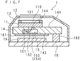
- FIG. 7 is a schematic cross-sectional view illustrating a configuration example of the radiation detector 1 according to Embodiment 3.
- the configuration of parts of the radiation detection apparatus 10 other than the radiation detector 1 is the same as that of Embodiment 1.
- the radiation detector 1 does not include a cooling unit such as the Peltier element 17 and the cold finger 172.
- the radiation detection element 11 is operable even without cooling by a cooling unit.
- the radiation detector 1 includes the shield plate 16.
- a connector 182 is connected to a part of the second surface 142 of the substrate 14.
- the connector 182 is disposed between the part of the second surface 142 and the bottom plate portion 18 and is connected to the bottom plate portion 18.
- the connector 182 includes wiring, and the wiring connects a circuit provided on the substrate 14 and a circuit outside the radiation detector 1. Electric power supply and signal input and output with respect to the radiation detection element 11 are performed through the connector 182.
- the radiation detection element 11 is in close contact with the first surface 141 of the substrate 14 directly or via an interposed object and seals one end of the through hole 144.
- the radiation detector 1 includes a closing plate 161 blocking the other end of the through hole 144.
- the closing plate 161 is disposed at a position facing the part of the second surface 142 to which the connector 182 is not connected.
- the closing plate 161 is in close contact with the second surface 142 directly or via an interposed object and seals the other end of the through hole 144.
- the closing plate 161 corresponds to a plate-shaped member.
- the radiation detector 1 includes the shield plate 16. In Embodiment 3, the shield plate 16 does not correspond to a plate-shaped member.
- the shield plate 16 is disposed at a position facing the closing plate 161. A gap is provided between the closing plate 161 and the shield plate 16.
- the shield plate 16 shields radiation incident from outside the shield plate 16 when viewed from the radiation detection element 11.
- the radiation detector 1 includes the closed space 15.
- the incident surface 110 of the radiation detection element 11 does not face the closed space 15.
- the inside of the closed space 15 is decompressed or filled with an inert or dry gas.
- the amplifier 151 is disposed in the closed space 15, and the signal output electrode 115 faces the closed space 15.
- the moisture getter 153 and/or the gas getter 154 is disposed at a position coming into contact with the gas in the closed space 15.
- the moisture getter 153 and/or the gas getter 154 is applied to a part of the closing plate 161, and the closing plate 161 is disposed such that the part of the closing plate 161 to which the moisture getter 153 and/or the gas getter 154 is applied faces the other end of the through hole 144.
- the moisture getter 153 and/or the gas getter 154 may not be of application type.
- Embodiment 3 water or gas adsorption to the amplifier 151 or the signal output electrode 115 is unlikely to occur even in a case where the radiation detector 1 is used in a normal-pressure or low-vacuum environment. Deterioration of the amplifier 151 or the signal output electrode 115 attributable to water or gas adsorption is prevented, degradation in the performance of the radiation detector 1 is suppressed, and degradation in radiation detection accuracy is suppressed.
- FIG. 8 is a schematic cross-sectional view illustrating a first example of the configuration of the radiation detector 1 according to Embodiment 4.
- the configuration of parts of the radiation detection apparatus 10 other than the radiation detector 1 is the same as that of Embodiment 1.
- the configurations of the bottom plate portion 18 and the cover 13 are the same as those of Embodiment 1, and the opening portion 131 is formed at the truncated part of the tip of the cover 13.
- the configurations of the radiation detection element 11 and the collimator 12 are the same as those of Embodiment 1.
- the radiation detection element 11 is disposed on the first surface 141 of the substrate 14, and a shield plate 7 is disposed at a position facing the second surface 142.
- the shield plate 7 corresponds to a plate-shaped member.
- An interposed object such as an adhesive may be interposed between the shield plate 7 and the second surface 142.
- the Peltier element 17 has a heat-absorbing part in thermal contact with the back surface of the shield plate 7 behind the surface of the shield plate 7 in contact with the substrate 14.
- the configurations of the Peltier element 17, the waterproof coating material 171, the cold finger 172, and the lead pin 181 are the same as those of Embodiment 1.
- the heat of the radiation detection element 11 is conducted to the heat-absorbing part of the Peltier element 17 through the substrate 14 and the shield plate 7 and released from the heat-dissipating part of the Peltier element 17 to the outside of the radiation detector 1 through the cold finger 172.
- the through hole 144 is formed in the substrate 14 and the substrate 14 has the first surface 141, the second surface 142, and the third surface 143.
- the amplifier 151 is mounted on the third surface 143.
- circuit elements other than the amplifier 151 are also mounted on the third surface 143. Every circuit element included in the circuit provided on the substrate 14 may be mounted on the third surface 143.
- the amplifier 151 is connected to the signal output electrode of the radiation detection element 11 via the bonding wire 152.
- the shield plate 7 includes a first shield plate 71, a second shield plate 72, and a third shield plate 73.
- the first shield plate 71, the second shield plate 72, and the third shield plate 73 are plate-shaped.
- the first shield plate 71 is disposed at a position facing the second surface 142 of the substrate 14, and the first shield plate 71 is in contact with the second surface 142.
- An interposed object such as an adhesive may be interposed between the first shield plate 71 and the second surface 142.
- the first shield plate 71, the second shield plate 72, and the third shield plate 73 are stacked and joined.
- the heat-absorbing part of the Peltier element 17 is in thermal contact with the third shield plate 73.
- the Peltier element 17 may be in direct contact with the third shield plate 73 or a thermally conductive substance may be interposed between the Peltier element 17 and the third shield plate 73.
- the shield plate 7 is made of a substance with somewhat high thermal conductivity.
- the first shield plate 71 and the second shield plate 72 are made of alumina and the third shield plate 73 is made of Kovar.
- FIG. 9 is a schematic perspective view illustrating the first shield plate 71 and the second shield plate 72
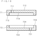
- FIG. 10 is a schematic cross-sectional view illustrating the first shield plate 71 and the second shield plate 72.
- the first shield plate 71 has a tray shape as a whole and has a top surface 713 corresponding to the upper surface of the edge of the tray and a recessed surface 714 surrounded by the top surface 713 in plan view and recessed from the top surface 713.
- the recessed surface 714 is wider than the top surface 713.
- the first shield plate 71 has a bottom surface 712 behind the top surface 713 and the recessed surface 714. The thickness from the bottom surface 712 to the recessed surface 714 is thinner than the thickness from the bottom surface 712 to the top surface 713.
- a connecting hole 711 penetrating the first shield plate 71 from the bottom surface 712 to the recessed surface 714 is formed in the first shield plate 71.
- FIG. 9 illustrates an example in which three connecting holes 711 are formed in the first shield plate 71.
- the number of connecting holes 711 may be two or less or may be four or more.
- the second shield plate 72 has the same shape as the first shield plate 71.
- the second shield plate 72 has connecting holes 721, a bottom surface 722, a top surface 723, and a recessed surface 724.
- the shield plate 7 is efficiently manufactured by the first shield plate 71 and the second shield plate 72 having the same shape.
- FIG. 9 illustrates an example in which the first shield plate 71 and the second shield plate 72 are hexagonal in plan view, the first shield plate 71 and the second shield plate 72 may have other shapes.
- the first shield plate 71 and the second shield plate 72 are stacked such that the top surface 713 and the top surface 723 face each other.
- the top surface 713 and the top surface 723 are closely attached and joined to each other.
- An interposed object such as an adhesive may be interposed between the first shield plate 71 and the second shield plate 72.
- the recessed surface 714 and the recessed surface 724 are not in contact with each other, and a space is sandwiched between the recessed surface 714 and the recessed surface 724.
- the space sandwiched between the recessed surface 714 and the recessed surface 724 is a cavity 74.
- the first shield plate 71 and the second shield plate 72 are stacked such that the connecting hole 711 and the connecting hole 721 do not face each other.
- the first shield plate 71 and the second shield plate 72 are stacked such that the connecting hole 711 and the connecting hole 721 do not overlap in plan view, and the connecting hole 711 and the connecting hole 721 are at different positions in plan view.
- the moisture getter 153 or the gas getter 154 is injected into the cavity 74 from the connecting hole 721.
- the moisture getter 153 or the gas getter 154 is not injected by an amount at which the cavity 74 is filled. Accordingly, the moisture getter 153 or the gas getter 154 does not reach the position of the connecting hole 711. In this manner, the moisture getter 153 or the gas getter 154 is disposed at a position in the cavity 74 different from the connecting hole 711.
- the third shield plate 73 is stacked and joined to the second shield plate 72 so as to be closely attached to the bottom surface 722. An interposed object such as an adhesive may be interposed between the second shield plate 72 and the third shield plate 73.
- the third shield plate 73 seals the connecting hole 721.
- the shield plate 7 is configured in this manner.
- the shield plate 7 is in close contact with the second surface 142 of the substrate 14.
- the diameter of the connecting hole 711 is smaller than the diameter of the through hole 144 in the second surface 142.
- the connecting hole 711 is disposed so as to face the other end of the through hole 144.
- a space 145 in the through hole 144 and the cavity 74 in the shield plate 7 are connected via the connecting hole 711.
- the space 145 and the cavity 74 connected to the space 145 via the connecting hole 711 form the closed space 15.
- One end of the through hole 144 is sealed by the radiation detection element 11, the connecting hole 721 is sealed by the third shield plate 73, and the closed space 15 is sealed as a result.
- the closed space 15 is decompressed or filled with an inert gas such as nitrogen gas or a dry gas such as dry carbon dioxide.
- an inert gas such as nitrogen gas or a dry gas such as dry carbon dioxide.
- circuit elements such as the amplifier 151 are disposed in the closed space 15, and the moisture getter 153 or the gas getter 154 is disposed in the closed space 15.
- the amplifier 151 is disposed in the closed space 15 and the signal output electrode 115 of the radiation detection element 11 faces the closed space 15. Accordingly, even in a case where the radiation detector 1 is used in a normal-pressure or low-vacuum environment, water or gas adsorption to the amplifier 151 or the signal output electrode 115 is unlikely to occur. Deterioration of the amplifier 151 or the signal output electrode 115 attributable to water or gas adsorption is prevented, degradation in the performance of the radiation detector 1 is suppressed, and degradation in radiation detection accuracy is suppressed.
- the moisture getter 153 or the gas getter 154 is disposed at a position different from the connecting hole 711, a part of the shield plate 7 is between the moisture getter 153 or the gas getter 154 and the radiation detection element 11. Accordingly, even in the event of characteristic X-ray generation from the moisture getter 153 or the gas getter 154, this characteristic X-ray is shielded by the shield plate 7 and is unlikely to be incident on the radiation detection element 11. Accordingly, a system peak attributable to incidence on the radiation detection element 11 of a characteristic X-ray generated from the moisture getter 153 or the gas getter 154 is unlikely to occur. As a result, degradation in radiation detection accuracy is further suppressed.
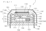
- FIG. 11 is a schematic cross-sectional view illustrating a second example of the configuration of the radiation detector 1 according to Embodiment 4.
- the radiation detection element 11 is operable even without cooling by a cooling unit.
- the radiation detector 1 does not include a cooling unit such as the Peltier element 17 and the cold finger 172.
- the third shield plate 73 included in the shield plate 7 is in close contact with the bottom plate portion 18 directly or via an interposed object.
- the heat of the radiation detection element 11 is conducted to the bottom plate portion 18 through the substrate 14 and the shield plate 7 and released from the bottom plate portion 18 to the outside of the radiation detector 1.
- the shield plate 7 may not include the third shield plate 73 and the connecting hole 721 may be blocked by the bottom plate portion 18.
- water or gas adsorption to the amplifier 151 or the signal output electrode 115 is unlikely to occur even in a case where the radiation detector 1 is used in a normal-pressure or low-vacuum environment. Deterioration of the amplifier 151 or the signal output electrode 115 attributable to water or gas adsorption is prevented. In addition, a characteristic X-ray generated from the moisture getter 153 or the gas getter 154 is unlikely to be incident on the radiation detection element 11, and a system peak attributable to the moisture getter 153 or the gas getter 154 is unlikely to occur. Accordingly, degradation in radiation detection accuracy is suppressed.
- the radiation detector 1 includes a housing in Embodiments 1 to 4, the radiation detector 1 may have no housing.
- the radiation detector 1 may be configured without the cover 13.
- the configuration of the part other than the housing of the radiation detector 1 is the same as those of Embodiments 1 to 4.
- the closed space 15 is disposed at a position that the incident surface 110 of the radiation detection element 11 does not face. In this form as well, water or gas adsorption to the amplifier 151 or the signal output electrode 115 is unlikely to occur and deterioration of the amplifier 151 or the signal output electrode 115 attributable to water or gas adsorption is prevented.
- the radiation detector 1 includes the amplifier 151 in the closed space 15.
- the radiation detector 1 may include circuit elements other than the amplifier 151 in addition to or in place of the amplifier 151 in the closed space 15.
- the radiation detection element 11 is a silicon drift-type radiation detection element in Embodiments 1 to 4, the radiation detection element 11 may be an element other than a silicon drift-type radiation detection element insofar as the radiation detection element 11 is a semiconductor element. Accordingly, the radiation detector 1 may be a non-SDD radiation detector.
- the sample 6 is irradiated with radiation and the radiation generated from the sample 6 is detected in Embodiments 1 to 4, the radiation detection apparatus 10 may detect radiation transmitted through the sample 6 or reflected by the sample 6.
- the radiation detection apparatus 10 may scan the sample 6 with radiation by changing the direction of the radiation.
- the radiation detection apparatus 10 may not include the irradiation unit 4, the sample table 5, the analysis unit 32, or the display unit 33.
Landscapes
- Physics & Mathematics (AREA)
- Health & Medical Sciences (AREA)
- Life Sciences & Earth Sciences (AREA)
- General Physics & Mathematics (AREA)
- High Energy & Nuclear Physics (AREA)
- Molecular Biology (AREA)
- Spectroscopy & Molecular Physics (AREA)
- Chemical & Material Sciences (AREA)
- Analytical Chemistry (AREA)
- Biochemistry (AREA)
- General Health & Medical Sciences (AREA)
- Immunology (AREA)
- Pathology (AREA)
- Measurement Of Radiation (AREA)
Abstract
Description
- The present invention relates to a radiation detector and a radiation detection apparatus.
- A radiation detector detecting radiation such as X-rays may include a radiation detection element using a semiconductor. In addition, the radiation detector is provided with a circuit element such as a preamplifier amplifying a signal output by the radiation detection element. The radiation detector includes a housing, and the radiation detection element and the circuit element are disposed inside the housing. For example, a substrate is disposed inside the housing, the radiation detection element is provided on the surface of the substrate, and the circuit element is provided on the back surface of the substrate. In many cases, the housing is provided with a window having a window material formed of a radiation-transmitting material. Radiation transmitted through the window material is detected. Radiation that cannot be transmitted through the window material due to the low energy thereof cannot be detected by the radiation detector. In this regard, radiation detectors have been developed that are capable of detecting low-energy radiation by window material elimination.
Patent Document 1 discloses an example of a window material-less radiation detector. - [Patent Document 1] International Publication No.
WO2019/117272 - In a case where the window material-less radiation detector is used in a normal-pressure or low-vacuum environment, a gas such as water vapor enters from the outside to the inside of the radiation detector. Gas adsorption to a circuit element in the radiation detector may occur to cause circuit element deterioration and degradation in the performance of the radiation detector.
- The present invention has been made in view of such circumstances, and an object of the present invention is to provide a radiation detector and a radiation detection apparatus capable of suppressing degradation in performance.
- A radiation detector according to the present invention includes a radiation detection element, a circuit element, and a housing accommodating the radiation detection element and the circuit element, is characterized in that a closed space is provided, the housing has an unblocked opening portion, the closed space is disposed inside the housing, the circuit element is disposed in the closed space, and the closed space is decompressed or filled with an inert gas or a dry gas.
- In one aspect of the present invention, the housing of the radiation detector has the unblocked opening portion. The radiation detector includes the closed space, and the circuit element such as an amplifier is disposed in the closed space. A gas such as water vapor is capable of entering the inside of the housing through the opening portion but does not enter the closed space. Accordingly, even in a case where the radiation detector is used in a normal-pressure or low-vacuum environment, the gas that has entered from the outside is not adsorbed to the circuit element. In addition, the inside of the closed space is decompressed or filled with an inert or dry gas. It is difficult for the water or gas in the closed space to be adsorbed to the circuit element, and a reaction degrading the circuit element is unlikely to occur even in the event of inert gas adsorption to the circuit element. Accordingly, deterioration of the circuit element attributable to water or gas adsorption is prevented.
- In the radiation detector according to the present invention, it is characterized in that the radiation detection element is disposed at a position facing the opening portion.
- In one aspect of the present invention, the radiation detection element faces the opening portion. The radiation incident on the radiation detection element passes through the opening portion and does not have to be transmitted through a window material. Accordingly, the radiation detector is capable of detecting radiation that cannot be transmitted through a window material due to the low energy thereof.
- A radiation detector according to the present invention includes a radiation detection element having an incident surface where radiation is incident and a circuit element, is characterized in that a closed space disposed at a position not facing the incident surface is provided, the circuit element is disposed in the closed space, and the closed space is decompressed or filled with an inert gas or a dry gas.
- In one aspect of the present invention, the radiation detector includes the closed space and the circuit element such as an amplifier is disposed in the closed space. The incident surface of the radiation detection element does not face the closed space. A gas such as water vapor does not enter the closed space. Accordingly, gas adsorption to the circuit element does not occur. In addition, the inside of the closed space is decompressed or filled with an inert or dry gas. Water or gas adsorption to the circuit element is unlikely to occur, and deterioration of the circuit element attributable to water or gas adsorption is prevented.
- In the radiation detector according to the present invention, it is characterized in that the radiation detection element has an electrode connected to the circuit element, and the electrode faces the closed space.
- In one aspect of the present invention, the radiation detection element includes the electrode for connection to the circuit element and the electrode faces the closed space. As a result, water or gas adsorption to the electrode is unlikely to occur. Even in the event of inert gas adsorption to the electrode, a reaction degrading the electrode is unlikely to occur. Accordingly, degradation in the performance of the radiation detection element attributable to electrode deterioration is prevented.
- The radiation detector according to the present invention, is characterized by further comprising a moisture getter taking in moisture in the closed space.
- In one aspect of the present invention, the moisture getter takes in the moisture in the closed space. Accordingly, water adsorption to the circuit element is more effectively prevented.
- The radiation detector according to the present invention, is characterized by further comprising a gas getter taking in a gas in the closed space.
- In one aspect of the present invention, the gas getter takes in the gas in the closed space. Accordingly, gas adsorption to the circuit element is more effectively prevented.
- The radiation detector according to the present invention, is characterized by further comprising: a substrate having a first surface and a second surface positioned behind the first surface; and a plate-shaped member, wherein the substrate has a through hole penetrating the substrate between the first surface and the second surface, the radiation detection element is disposed on the first surface and blocks one end of the through hole, the plate-shaped member is disposed so as to face the second surface and blocks the other end of the through hole, and the closed space is a space in the through hole blocked at both ends by the radiation detection element and the plate-shaped member.
- In one aspect of the present invention, the radiation detector includes the substrate having the through hole, the radiation detection element is disposed so as to block one end of the through hole, and the plate-shaped member is disposed so as to block the other end of the through hole. The space in the through hole is to be the closed space by the radiation detection element and the plate-shaped member blocking both ends of the through hole. The closed space where no gas enters is configured with ease.
- The radiation detector according to the present invention, is characterized by further comprising: a substrate having a first surface and a second surface positioned behind the first surface; and a plate-shaped member having a cavity inside, wherein the substrate has a through hole penetrating the substrate between the first surface and the second surface, the radiation detection element is disposed on the first surface and blocks one end of the through hole, the plate-shaped member is disposed so as to face the second surface and blocks the other end of the through hole, the plate-shaped member has a connecting hole smaller in diameter than the through hole and connecting a space in the through hole and the cavity, at a part facing the second surface, the closed space includes the space in the through hole blocked at both ends by the radiation detection element and the plate-shaped member and the cavity connected to the space via the connecting hole, and a moisture getter taking in moisture in the closed space or a gas getter taking in a gas in the closed space is disposed at a position in the cavity different from the connecting hole.
- In one aspect of the present invention, the radiation detector includes the substrate having the through hole, the radiation detection element is disposed so as to block one end of the through hole, and the plate-shaped member is disposed so as to block the other end of the through hole. The plate-shaped member has the cavity inside and has the connecting hole connecting the space in the through hole and the cavity. The closed space including the space in the through hole and the cavity connected to the space via the connecting hole is configured. The moisture getter or the gas getter is disposed at the position in the cavity different from the connecting hole. A part of a shield plate is between the moisture getter or the gas getter and the radiation detection element, and characteristic X-rays from the moisture getter or the gas getter are shielded by the shield plate. Accordingly, a system peak attributable to the moisture getter or the gas getter is unlikely to occur.
- The radiation detector according to the present invention, is characterized by further comprising a cooling unit for cooling the radiation detection element.
- In one aspect of the present invention, the radiation detector includes the cooling unit such as a Peltier element for cooling the radiation detection element. The cooling of the radiation detection element leads to noise reduction and radiation detection accuracy improvement. Even with the radiation detection element cooled, adsorption of a gas such as water vapor to the circuit element is prevented.
- In the radiation detector according to the present invention, it is characterized in that
the circuit element configures at least a part of an amplifier circuit amplifying a signal output by the radiation detection element. - In one aspect of the present invention, the circuit element configures at least a part of the amplifier circuit. Deterioration of the amplifier circuit is prevented, and thus deterioration of the signal output from the radiation detector is prevented and degradation in radiation detection accuracy is suppressed.
- A radiation detection apparatus according to the present invention, is characterized by comprising: the radiation detector according to the present invention; and a spectrum generation unit generating a spectrum of radiation detected by the radiation detector.
- A radiation detection apparatus according to the present invention, is characterized by comprising: an irradiation unit irradiating a sample with radiation; the radiation detector according to the present invention detecting radiation generated from the sample; a spectrum generation unit generating a spectrum of the radiation detected by the radiation detector; and a display unit displaying the spectrum generated by the spectrum generation unit.
- In one aspect of the present invention, deterioration of the circuit element attributable to gas adsorption to the circuit element of the radiation detector is prevented. Accordingly, degradation in the performance of the radiation detector is suppressed. In particular, even in a case where the window material-less radiation detector is used in a normal-pressure or low-vacuum environment, degradation in the performance of the radiation detector is suppressed.
- According to the present invention, amplifier deterioration attributable to water or gas adsorption is prevented, and thus excellent effects such as suppressing degradation in the performance of the radiation detector are exhibited.
-
-
FIG. 1 is a schematic perspective view illustrating an example of the appearance of a radiation detector according toEmbodiment 1. -
FIG. 2 is a schematic cross-sectional view illustrating a configuration example of the radiation detector according toEmbodiment 1. -
FIG. 3 is a block diagram illustrating a functional configuration example of a radiation detection apparatus. -
FIG. 4 is a schematic cross-sectional view illustrating a radiation detection element and a collimator. -
FIG. 5 is an enlarged schematic cross-sectional view of the part where the radiation detection element, a substrate, and a shield plate according toEmbodiment 1 are joined. -
FIG. 6 is a schematic cross-sectional view illustrating a configuration example of a radiation detector according toEmbodiment 2. -
FIG. 7 is a schematic cross-sectional view illustrating a configuration example of a radiation detector according to Embodiment 3. -
FIG. 8 is a schematic cross-sectional view illustrating a first example of the configuration of a radiation detector according to Embodiment 4. -
FIG. 9 is a schematic perspective view illustrating a first shield plate and a second shield plate. -
FIG. 10 is a schematic cross-sectional view illustrating the first shield plate and the second shield plate. -
FIG. 11 is a schematic cross-sectional view illustrating a second example of the configuration of the radiation detector according to Embodiment 4. - Hereinafter, the present invention will be specifically described with reference to the drawings illustrating embodiments thereof.
-
FIG. 1 is a schematic perspective view illustrating an example of the appearance of aradiation detector 1 according toEmbodiment 1.FIG. 2 is a schematic cross-sectional view illustrating a configuration example of theradiation detector 1 according toEmbodiment 1. -
FIG. 3 is a block diagram illustrating a functional configuration example of aradiation detection apparatus 10. Theradiation detection apparatus 10 is, for example, a fluorescent X-ray analyzer. Theradiation detection apparatus 10 includes an irradiation unit 4 irradiating asample 6 with radiation such as electron beams or X-rays, a sample table 5 where thesample 6 is placed, and theradiation detector 1. Radiation is emitted from the irradiation unit 4 to thesample 6, radiation such as fluorescent X-rays is generated at thesample 6, and theradiation detector 1 detects the radiation generated from thesample 6. In the drawing, the radiation is indicated by arrows. Theradiation detector 1 outputs a signal proportional to the energy of the detected radiation. It should be noted that theradiation detection apparatus 10 in another form may hold thesample 6 by a method other than placement on the sample table 5. - Connected to the
radiation detector 1 are asignal processing unit 2 processing the output signal and avoltage application unit 34 applying a voltage necessary for radiation detection to aradiation detection element 11 of theradiation detector 1. Thesignal processing unit 2 detects a signal value corresponding to the energy of the radiation detected by theradiation detector 1 by detecting the wave height of the pulse signal output by theradiation detector 1. Ananalysis unit 32 is connected to thesignal processing unit 2. Theanalysis unit 32 is configured to include a calculation unit performing calculation and a memory storing data. Thesignal processing unit 2, theanalysis unit 32, thevoltage application unit 34, and the irradiation unit 4 are connected to acontrol unit 31. Thecontrol unit 31 controls the operations of thesignal processing unit 2, theanalysis unit 32, thevoltage application unit 34, and the irradiation unit 4. - The
signal processing unit 2 outputs data indicating the detected signal value to theanalysis unit 32. Based on the data from thesignal processing unit 2, theanalysis unit 32 counts the signal of each value and performs processing to generate the relationship between the energy of the radiation and the count number, that is, the spectrum of the radiation. Thesignal processing unit 2 and theanalysis unit 32 correspond to a spectrum generation unit. In addition, theanalysis unit 32 performs qualitative analysis or quantitative analysis of elements contained in thesample 6 based on the spectrum. It should be noted that thesignal processing unit 2 may generate the radiation spectrum. - A
display unit 33 such as a liquid crystal display is connected to theanalysis unit 32. Thedisplay unit 33 displays the spectrum generated by theanalysis unit 32 and the analysis result by theanalysis unit 32. Thecontrol unit 31 may be configured to receive a user operation and control each unit of theradiation detection apparatus 10 in accordance with the received operation. In addition, thecontrol unit 31 and theanalysis unit 32 may be configured by the same computer. - As illustrated in
FIGS. 1 and2 , theradiation detector 1 includes a plate-shapedbottom plate portion 18. One surface side of thebottom plate portion 18 is covered with a cap-shapedcover 13. Thecover 13 has a shape in which a truncated cone is connected to one end of a cylinder, and the other end of the cylinder is joined to thebottom plate portion 18. Anopening portion 131 is formed at the truncated part of the tip of thecover 13. A window having a window material is not provided in theopening portion 131, and theopening portion 131 is blocked by no window materials. Thecover 13 and thebottom plate portion 18 configure the housing of theradiation detector 1. Thecover 13 and thebottom plate portion 18 accommodate other parts of theradiation detector 1. Gas can be exchanged between the inside and outside of thecover 13 and thebottom plate portion 18. - The
radiation detection element 11, acollimator 12, asubstrate 14, ashield plate 16, aPeltier element 17, and acold finger 172 are disposed inside thecover 13. Thesubstrate 14 has afirst surface 141 facing theopening portion 131, and theradiation detection element 11 is disposed on thefirst surface 141. An interposed object such as an adhesive may be present between thesubstrate 14 and theradiation detection element 11. Thesubstrate 14 is desirably formed of a material that generates as little radiation as possible when irradiated with radiation. The material of thesubstrate 14 is, for example, ceramic. For example, theradiation detection element 11 is a silicon drift-type radiation detection element, and theradiation detector 1 is a silicon drift detector (SDD). For example, theradiation detection element 11 is plate-shaped. Theradiation detection element 11 is disposed at a position facing theopening portion 131. Theradiation detection element 11 has anincident surface 110 where radiation to be detected is incident, and theincident surface 110 is disposed so as to face theopening portion 131. - The
collimator 12 has a tubular shape with both ends open and is made of a radiation shielding material. Thecollimator 12 is disposed between theradiation detection element 11 and theopening portion 131. One end of thecollimator 12 faces theopening portion 131, and the other end faces theincident surface 110 of theradiation detection element 11. Anadhesive layer 121 consisting of an insulating adhesive and coating is provided between thecollimator 12 and theradiation detection element 11. Thecollimator 12 is attached to theincident surface 110 of theradiation detection element 11 via theadhesive layer 121. Radiation is incident on the inside of thecover 13 mainly through theopening portion 131, thecollimator 12 shields part of the radiation, and theradiation detection element 11 detects the radiation not shielded by thecollimator 12. - The
substrate 14 has asecond surface 142 positioned behind thefirst surface 141. Theshield plate 16 is disposed at a position facing thesecond surface 142. Theshield plate 16 corresponds to a plate-shaped member. Theshield plate 16 shields radiation incident from outside theshield plate 16 when viewed from theradiation detection element 11. Theshield plate 16 is in contact with thesecond surface 142. An interposed object such as an adhesive may be interposed between theshield plate 16 and thesecond surface 142. - The
Peltier element 17 has a heat-absorbing part that is in thermal contact with the back surface of theshield plate 16 behind the surface of theshield plate 16 in contact with thesubstrate 14. ThePeltier element 17 may be in direct contact with theshield plate 16 or a thermally conductive substance may be interposed between thePeltier element 17 and theshield plate 16. Awaterproof coating material 171 is applied around the part where thePeltier element 17 and theshield plate 16 are in contact with each other. Thewaterproof coating material 171 is, for example, a waterproof resin. Thewaterproof coating material 171 prevents water generated by cooling from entering between thePeltier element 17 and theshield plate 16. - The
Peltier element 17 has a heat-dissipating part that is in thermal contact with thecold finger 172. Thecold finger 172 is configured to include a flat plate-shaped part with which the heat-dissipating part of thePeltier element 17 is in thermal contact and a bolt-shaped part protruding from the flat plate-shaped part. The bolt-shaped part of thecold finger 172 penetrates thebottom plate portion 18 and protrudes from the outer surface of thebottom plate portion 18. ThePeltier element 17 may be in direct contact with thecold finger 172 or a thermally conductive substance may be interposed between thePeltier element 17 and thecold finger 172. Thecold finger 172 is formed of a material with high thermal conductivity. The bolt-shaped part of thecold finger 172 is connected to a heat-dissipating portion outside theradiation detector 1. The heat-dissipating portion is, for example, a heat sink. - The heat of the
radiation detection element 11 is conducted to the heat-absorbing part of thePeltier element 17 through thesubstrate 14 and theshield plate 16. The heat is released from the heat-dissipating part of thePeltier element 17 to the outside of theradiation detector 1 through thecold finger 172. In this manner, the heat of theradiation detection element 11 is released to the outside of theradiation detector 1 and theradiation detection element 11 is cooled. ThePeltier element 17 corresponds to a cooling unit. Theshield plate 16 is desirably made of a thermally conductive material higher in thermal conductivity than thesubstrate 14 such that the heat of theradiation detection element 11 can be efficiently conducted to thePeltier element 17. For example, the material of theshield plate 16 is alumina. The thermal conductivity of alumina is somewhat high. In addition, aluminum contained in alumina has low excitation efficiency by radiation and causes few system peaks attributable to characteristic X-rays generated from aluminum being incident on theradiation detection element 11. It should be noted that theradiation detector 1 in another form may release heat through thebottom plate portion 18 without including thecold finger 172. - The
substrate 14 is provided with anamplifier 151 as will be described later. Theamplifier 151 corresponds to a circuit element. Theamplifier 151 is connected to theradiation detection element 11 via abonding wire 152. In addition, thesubstrate 14 is provided with a circuit. Theamplifier 151 is connected to the circuit. The circuit may include a circuit element other than theamplifier 151. - The
radiation detector 1 further includes a plurality of lead pins 181. Thelead pin 181 penetrates thebottom plate portion 18. One end of thelead pin 181 is connected via a bonding wire to the circuit provided on thesubstrate 14. Electric power supply and signal input and output with respect to theradiation detection element 11 are performed through the lead pins 181. - The
amplifier 151 configures at least a part of an amplifier circuit amplifying the signal output by theradiation detection element 11. For example, other parts of the amplifier circuit are included in thesignal processing unit 2. For example, theamplifier 151 is a preamplifier. Theradiation detection element 11 outputs a signal proportional to the energy of the detected radiation, and the output signal is input to theamplifier 151 through thebonding wire 152. Theamplifier 151 performs signal conversion and amplification. The converted and amplified signal is output from theamplifier 151 and output to the outside of theradiation detector 1 through thelead pin 181. In this manner, theradiation detector 1 outputs a signal proportional to the energy of the radiation detected by theradiation detection element 11. The output signal is input to thesignal processing unit 2. It should be noted that theamplifier 151 may have a non-preamplifier function. -
FIG. 4 is a schematic cross-sectional view illustrating theradiation detection element 11 and thecollimator 12. A part of theincident surface 110 of theradiation detection element 11 is covered with thecollimator 12 and theadhesive layer 121. The part that includes the middle part of theincident surface 110 and is not covered with thecollimator 12 and theadhesive layer 121 is covered with alight shielding film 111. - The
radiation detection element 11 has a plate-shapedsemiconductor portion 112. The component of thesemiconductor portion 112 is, for example, n-type silicon (Si). Theincident surface 110 of theradiation detection element 11 is provided with afirst electrode 113. Thefirst electrode 113 is continuously provided in the region that includes the middle part of theincident surface 110. Thefirst electrode 113 is provided up to the vicinity of the peripheral edge of theincident surface 110 and occupies most of theincident surface 110. Thefirst electrode 113 is connected to thevoltage application unit 34. Multiple loop-shapedsecond electrodes 114 are provided on the back surface of theradiation detection element 11 behind theincident surface 110. In addition, asignal output electrode 115 outputting a signal during radiation detection is provided at the position surrounded by the multiplesecond electrodes 114. Thesignal output electrode 115 is connected to theamplifier 151 via thebonding wire 152. Of the multiplesecond electrodes 114, thesecond electrode 114 closest to thesignal output electrode 115 and thesecond electrode 114 farthest from thesignal output electrode 115 are connected to thevoltage application unit 34. - The
voltage application unit 34 performs voltage application to the multiplesecond electrodes 114 such that thesecond electrode 114 closest to thesignal output electrode 115 has the highest potential and thesecond electrode 114 farthest from thesignal output electrode 115 has the lowest potential. In addition, theradiation detection element 11 is configured such that a predetermined electrical resistance is generated between the adjacentsecond electrodes 114. For example, by adjusting the chemical composition of a part of thesemiconductor portion 112 positioned between the adjacentsecond electrodes 114, an electrically resistive channel to which twosecond electrodes 114 are connected is formed. In other words, the multiplesecond electrodes 114 are connected in a daisy chain via electrical resistance. By applying a voltage from thevoltage application unit 34 to the multiplesecond electrodes 114, the respectivesecond electrodes 114 have potentials that monotonically increase in order from thesecond electrode 114 far from thesignal output electrode 115 toward thesecond electrode 114 close to thesignal output electrode 115. It should be noted that the plurality ofsecond electrodes 114 may include a pair of adjacentsecond electrodes 114 with the same potential. - The potentials of the plurality of
second electrodes 114 generate an electric field in thesemiconductor portion 112, in which the potential increases in stages as the distance to thesignal output electrode 115 decreases and decreases in stages as the distance to thesignal output electrode 115 increases. Further, thevoltage application unit 34 applies a voltage to thefirst electrode 113 such that thefirst electrode 113 is lower in potential than thesecond electrode 114 with the highest potential. In this manner, a voltage is applied to thesemiconductor portion 112 between thefirst electrode 113 and thesecond electrodes 114, and an electric field with a potential increasing as the distance to thesignal output electrode 115 decreases is generated in thesemiconductor portion 112. - The
radiation detector 1 is disposed such that theopening portion 131 faces the placement surface of the sample table 5. Radiation from thesample 6 is incident on theradiation detection element 11 through theopening portion 131. The radiation is absorbed by thesemiconductor portion 112, and electric charges corresponding in amount to the energy of the absorbed radiation are generated. The generated electric charges are electrons and holes. The generated electric charges are moved by the electric field in thesemiconductor portion 112, and one type of electric charge flows into thesignal output electrode 115. In the present embodiment, in a case where thesignal output electrode 115 is n-type, electrons generated by radiation incidence move and flow into thesignal output electrode 115. The electric charge that has flowed into thesignal output electrode 115 is output as a current signal and input to theamplifier 151. As described above, theamplifier 151 converts and amplifies the signal, and the converted and amplified signal is output from theamplifier 151. As a result, theradiation detector 1 outputs a signal proportional to the radiation energy. -
FIG. 5 is an enlarged schematic cross-sectional view of the part where theradiation detection element 11, thesubstrate 14, and theshield plate 16 according toEmbodiment 1 are joined. InFIG. 5 , the parts of theradiation detector 1 other than theradiation detection element 11, thesubstrate 14, and theshield plate 16 are omitted, and the structure of theradiation detection element 11 is omitted except for thesignal output electrode 115. A throughhole 144 penetrating thesubstrate 14 between thefirst surface 141 and thesecond surface 142 is formed in thesubstrate 14. One end of the throughhole 144 is open to thefirst surface 141, and the other end of the throughhole 144 is open to thesecond surface 142. The shape of the throughhole 144 is greatly expanded midway from one end toward the other end. The size of the other end of the throughhole 144 is larger than the size of one end of the throughhole 144. The shape of the throughhole 144 is substantially constant from one end to the expanded part and substantially constant from the expanded part to the other end. The shapes of one end and the other end of the throughhole 144 may be circular or polygonal. The shapes of one end and the other end of the throughhole 144 may be the same or different. - A planar
third surface 143 is formed on the inner surface of the throughhole 144. Thethird surface 143 is substantially parallel to thefirst surface 141 and thesecond surface 142, is positioned behind thefirst surface 141, and faces theshield plate 16. Theamplifier 151 is mounted on thethird surface 143. - Both ends of the through
hole 144 are blocked by theradiation detection element 11 and theshield plate 16. Theradiation detection element 11 is disposed at the position where one end of the throughhole 144 is blocked. In addition, theradiation detection element 11 is in close contact with thefirst surface 141 directly or via an interposed object and seals one end of the throughhole 144. Theshield plate 16 faces thesecond surface 142 and thethird surface 143 of thesubstrate 14 and is disposed at the position where the other end of the throughhole 144 is blocked. Theshield plate 16 is in close contact with thesecond surface 142 directly or via an interposed object and seals the other end of the throughhole 144. - The space in the through
hole 144 blocked at both ends forms a sealedclosed space 15. In the related art, a space in a through hole formed in a substrate is connected to an opening portion in a side surface of the substrate, and no closed spaces are formed. In the present embodiment, the space in the throughhole 144 blocked at both ends is connected to no opening portions. Gas exchange does not occur between the inside and outside of the closedspace 15. Theclosed space 15 is decompressed or filled with an inert gas such as nitrogen gas or a dry gas such as dry carbon dioxide. Theclosed space 15 is not filled with a solid or liquid substance such as resin. For example, the closedspace 15 is formed by joining theradiation detection element 11 and theshield plate 16 to thesubstrate 14 in a decompressed space or a space filled with an inert or dry gas. Since theradiation detection element 11, thesubstrate 14, and theshield plate 16 are disposed inside thecover 13, the closedspace 15 is also disposed inside thecover 13. Theincident surface 110 of theradiation detection element 11 does not face the closedspace 15. A part of the back surface of theradiation detection element 11 faces the closedspace 15. - The
third surface 143 is in the closedspace 15. Accordingly, theamplifier 151 is disposed in the closedspace 15. In addition, theradiation detection element 11 is disposed at the position where thesignal output electrode 115 faces one end of the throughhole 144. Accordingly, thesignal output electrode 115 faces the closedspace 15. Thebonding wire 152 connects theamplifier 151 to theradiation detection element 11 by being positioned in the closedspace 15 with one end connected to thesignal output electrode 115 and the other end connected to theamplifier 151. - Further, the
radiation detector 1 includes amoisture getter 153 taking in moisture in the closedspace 15. Themoisture getter 153 is disposed at a position coming into contact with the gas in the closedspace 15. Themoisture getter 153 takes in the moisture contained in the gas in the closedspace 15 by water vapor adsorption or water absorption. For example, themoisture getter 153 is an application-type desiccant and is applied to the surface of theshield plate 16 facing the closedspace 15. Themoisture getter 153 is applied to a part of the surface of theshield plate 16, and theshield plate 16 is disposed at the position where the part of theshield plate 16 to which themoisture getter 153 is applied faces the other end of the throughhole 144. Themoisture getter 153 may not be of application type. For example, themoisture getter 153 may be a solid substance disposed in the closedspace 15. - Further, the
radiation detector 1 may be provided with agas getter 154 taking in the gas in the closedspace 15 instead of or in addition to themoisture getter 153. Thegas getter 154 is disposed at a position coming into contact with the gas in the closedspace 15. Thegas getter 154 takes in the gas in the closedspace 15 by gas adsorption. Thegas getter 154 has the property of taking in a gas other than water vapor. The gas taken in by thegas getter 154 is, for example, carbon dioxide. Thegas getter 154 may have the property of taking in a plurality of types of gases and may also have the property of taking in water vapor. Thegas getter 154 is applied to a part of the surface of theshield plate 16, and theshield plate 16 is disposed at the position where the part of theshield plate 16 to which thegas getter 154 is applied faces the other end of the throughhole 144. Thegas getter 154 may not be of application type. For example, thegas getter 154 may be a solid substance disposed in the closedspace 15. - As described above, the
radiation detector 1 includes the closedspace 15 and theamplifier 151 is disposed in the closedspace 15. In a case where theradiation detector 1 is used in a normal-pressure or low-vacuum environment, a gas such as water vapor is capable of entering the inside of thecover 13 through theopening portion 131. However, although the closedspace 15 is inside thecover 13, the closedspace 15 is sealed, and thus no gases enter the closedspace 15. Accordingly, even in a case where theradiation detector 1 is used in a normal-pressure or low-vacuum environment, the gas that has entered from the outside of theradiation detector 1 is not adsorbed to theamplifier 151. In addition, the inside of the closedspace 15 is decompressed or filled with an inert or dry gas. Accordingly, it is difficult for the water or gas in the closedspace 15 to be adsorbed to theamplifier 151. Even in the event of inert gas adsorption to theamplifier 151, a reaction degrading theamplifier 151 is unlikely to occur. Accordingly, deterioration of theamplifier 151 attributable to water or gas adsorption is prevented, and degradation in the performance of theradiation detector 1 is suppressed. Since deterioration of theamplifier 151 is prevented, deterioration of the signal output from theradiation detector 1 is prevented and degradation in radiation detection accuracy is suppressed. - The
signal output electrode 115 faces the closedspace 15, and thus water or gas adsorption to thesignal output electrode 115 is unlikely to occur. Even in the event of inert gas adsorption to thesignal output electrode 115, a reaction degrading thesignal output electrode 115 is unlikely to occur. Accordingly, degradation in the performance of theradiation detection element 11 attributable to deterioration of thesignal output electrode 115 is prevented, and degradation in the performance of theradiation detector 1 is suppressed. - The radiation detector of the related art that has an opening portion not blocked by a window material is problematic in that the detector deteriorates more quickly than a radiation detector provided with a window having a window material. In developing a radiation detector with an unblocked opening portion, it has been found that a gas adhering to an amplifier and a signal output electrode is a main cause of deterioration. In the present embodiment, by making the space around the
amplifier 151 and thesignal output electrode 115 the closedspace 15, water or gas adsorption to theamplifier 151 and thesignal output electrode 115 is prevented as much as possible. The occurrence of the main cause of deterioration of theradiation detector 1 is prevented, and degradation in the performance of theradiation detector 1 is suppressed. - The
closed space 15 is not filled with a solid or liquid substance such as resin. In a case where the closedspace 15 is filled with a solid or liquid substance, the capacitance of theradiation detection element 11 increases and the signal-to-noise (SN) ratio of the signal output by theradiation detection element 11 deteriorates. In the present embodiment, the closedspace 15 is not filled with a solid or liquid substance, and thus the capacitance of theradiation detection element 11 is not increased by the substance with which the closedspace 15 is filled and the SN ratio does not deteriorate. - Since the
moisture getter 153 is disposed in the closedspace 15, the water in the closedspace 15 is taken into themoisture getter 153. Accordingly, water adsorption to theamplifier 151 and thesignal output electrode 115 is more effectively prevented. In addition, since thegas getter 154 is disposed in the closedspace 15, the gas in the closedspace 15 is taken into thegas getter 154. Accordingly, adsorption of the gas in the closedspace 15 to theamplifier 151 and thesignal output electrode 115 is more effectively prevented. Deterioration of theamplifier 151 and thesignal output electrode 115 attributable to water or gas adsorption is more effectively prevented, and degradation in the performance of theradiation detector 1 is suppressed. - In the present embodiment, the
radiation detector 1 includes thePeltier element 17, and thePeltier element 17 cools theradiation detection element 11. The cooling of theradiation detection element 11 leads to noise reduction and radiation detection accuracy improvement. By cooling theradiation detection element 11, adsorption of a gas such as water vapor to theamplifier 151 becomes easier. However, in the present embodiment, since theamplifier 151 is disposed in the closedspace 15, gas adsorption to theamplifier 151 is prevented. Accordingly, the accuracy of radiation detection is improved while suppressing degradation in the performance of theradiation detector 1. - In addition, since the
opening portion 131 is not blocked by a window material, the radiation incident on theradiation detection element 11 does not have to be transmitted through a window material. Accordingly, theradiation detector 1 is capable of detecting radiation that cannot be transmitted through a window material due to the low energy thereof. For example, it is possible to detect an element with low fluorescent X-ray energy by detecting low-energy fluorescent X-rays. In the present embodiment, it is possible to suppress degradation in the performance of theradiation detector 1 while enabling detection of low-energy radiation. Even in a case where theradiation detector 1 is used in a normal-pressure or low-vacuum environment, deterioration of theamplifier 151 attributable to water or gas adsorption is prevented and degradation in the performance of theradiation detector 1 is suppressed. - Although the
radiation detector 1 in the present embodiment includes thePeltier element 17 as a cooling unit, theradiation detector 1 may include a cooling unit other than thePeltier element 17. Alternatively, theradiation detector 1 may include no cooling units. -
Embodiment 2 illustrates an example in which theradiation detector 1 includes no cooling units.FIG. 6 is a schematic cross-sectional view illustrating a configuration example of theradiation detector 1 according toEmbodiment 2. The configuration of parts of theradiation detection apparatus 10 other than theradiation detector 1 is the same as that ofEmbodiment 1. Theradiation detection element 11 is operable even without cooling by a cooling unit. Theradiation detector 1 does not include theshield plate 16, thePeltier element 17, and thecold finger 172. - The
second surface 142 of thesubstrate 14 faces thebottom plate portion 18. Both ends of the throughhole 144 formed in thesubstrate 14 are blocked by theradiation detection element 11 and thebottom plate portion 18. Theradiation detection element 11 is in close contact with thefirst surface 141 directly or via an interposed object and seals one end of the throughhole 144. Thebottom plate portion 18 blocks the other end of the throughhole 144. Thebottom plate portion 18 is in close contact with thesecond surface 142 directly or via an interposed object and seals the other end of the throughhole 144. InEmbodiment 2, thebottom plate portion 18 corresponds to a plate-shaped member. The heat of theradiation detection element 11 is conducted to thebottom plate portion 18 through thesubstrate 14 and released from thebottom plate portion 18 to the outside of theradiation detector 1. - The space in the through
hole 144 blocked at both ends forms the sealedclosed space 15. In other words, also inEmbodiment 2, theradiation detector 1 includes the closedspace 15. Theincident surface 110 of theradiation detection element 11 does not face the closedspace 15. The inside of the closedspace 15 is decompressed or filled with an inert or dry gas. Theamplifier 151 is disposed in the closedspace 15, and thesignal output electrode 115 faces the closedspace 15. In addition, themoisture getter 153 and/or thegas getter 154 is disposed at a position coming into contact with the gas in the closedspace 15. Themoisture getter 153 and/or thegas getter 154 is applied to a part of the surface of thebottom plate portion 18, and thesubstrate 14 is disposed with respect to thebottom plate portion 18 such that the part of thebottom plate portion 18 to which themoisture getter 153 and/or thegas getter 154 is applied faces the other end of the throughhole 144. Themoisture getter 153 and/or thegas getter 154 may not be of application type. - In
Embodiment 2 as well asEmbodiment 1, water or gas adsorption to theamplifier 151 or thesignal output electrode 115 is unlikely to occur even in a case where theradiation detector 1 is used in a normal-pressure or low-vacuum environment. Deterioration of theamplifier 151 or thesignal output electrode 115 attributable to water or gas adsorption is prevented, degradation in the performance of theradiation detector 1 is suppressed, and degradation in radiation detection accuracy is suppressed. -
FIG. 7 is a schematic cross-sectional view illustrating a configuration example of theradiation detector 1 according to Embodiment 3. The configuration of parts of theradiation detection apparatus 10 other than theradiation detector 1 is the same as that ofEmbodiment 1. Also in Embodiment 3, theradiation detector 1 does not include a cooling unit such as thePeltier element 17 and thecold finger 172. Theradiation detection element 11 is operable even without cooling by a cooling unit. - The
radiation detector 1 includes theshield plate 16. Aconnector 182 is connected to a part of thesecond surface 142 of thesubstrate 14. Theconnector 182 is disposed between the part of thesecond surface 142 and thebottom plate portion 18 and is connected to thebottom plate portion 18. Theconnector 182 includes wiring, and the wiring connects a circuit provided on thesubstrate 14 and a circuit outside theradiation detector 1. Electric power supply and signal input and output with respect to theradiation detection element 11 are performed through theconnector 182. - The
radiation detection element 11 is in close contact with thefirst surface 141 of thesubstrate 14 directly or via an interposed object and seals one end of the throughhole 144. Theradiation detector 1 includes aclosing plate 161 blocking the other end of the throughhole 144. Theclosing plate 161 is disposed at a position facing the part of thesecond surface 142 to which theconnector 182 is not connected. Theclosing plate 161 is in close contact with thesecond surface 142 directly or via an interposed object and seals the other end of the throughhole 144. Theclosing plate 161 corresponds to a plate-shaped member. Theradiation detector 1 includes theshield plate 16. In Embodiment 3, theshield plate 16 does not correspond to a plate-shaped member. Theshield plate 16 is disposed at a position facing theclosing plate 161. A gap is provided between the closingplate 161 and theshield plate 16. Theshield plate 16 shields radiation incident from outside theshield plate 16 when viewed from theradiation detection element 11. - The space in the through
hole 144 blocked at both ends forms the sealedclosed space 15. In other words, also in Embodiment 3, theradiation detector 1 includes the closedspace 15. Theincident surface 110 of theradiation detection element 11 does not face the closedspace 15. The inside of the closedspace 15 is decompressed or filled with an inert or dry gas. Theamplifier 151 is disposed in the closedspace 15, and thesignal output electrode 115 faces the closedspace 15. In addition, themoisture getter 153 and/or thegas getter 154 is disposed at a position coming into contact with the gas in the closedspace 15. Themoisture getter 153 and/or thegas getter 154 is applied to a part of theclosing plate 161, and theclosing plate 161 is disposed such that the part of theclosing plate 161 to which themoisture getter 153 and/or thegas getter 154 is applied faces the other end of the throughhole 144. Themoisture getter 153 and/or thegas getter 154 may not be of application type. - In Embodiment 3 as well as
Embodiment 1, water or gas adsorption to theamplifier 151 or thesignal output electrode 115 is unlikely to occur even in a case where theradiation detector 1 is used in a normal-pressure or low-vacuum environment. Deterioration of theamplifier 151 or thesignal output electrode 115 attributable to water or gas adsorption is prevented, degradation in the performance of theradiation detector 1 is suppressed, and degradation in radiation detection accuracy is suppressed. -
FIG. 8 is a schematic cross-sectional view illustrating a first example of the configuration of theradiation detector 1 according to Embodiment 4. The configuration of parts of theradiation detection apparatus 10 other than theradiation detector 1 is the same as that ofEmbodiment 1. The configurations of thebottom plate portion 18 and thecover 13 are the same as those ofEmbodiment 1, and theopening portion 131 is formed at the truncated part of the tip of thecover 13. The configurations of theradiation detection element 11 and thecollimator 12 are the same as those ofEmbodiment 1. Theradiation detection element 11 is disposed on thefirst surface 141 of thesubstrate 14, and a shield plate 7 is disposed at a position facing thesecond surface 142. The shield plate 7 corresponds to a plate-shaped member. An interposed object such as an adhesive may be interposed between the shield plate 7 and thesecond surface 142. - The
Peltier element 17 has a heat-absorbing part in thermal contact with the back surface of the shield plate 7 behind the surface of the shield plate 7 in contact with thesubstrate 14. The configurations of thePeltier element 17, thewaterproof coating material 171, thecold finger 172, and thelead pin 181 are the same as those ofEmbodiment 1. The heat of theradiation detection element 11 is conducted to the heat-absorbing part of thePeltier element 17 through thesubstrate 14 and the shield plate 7 and released from the heat-dissipating part of thePeltier element 17 to the outside of theradiation detector 1 through thecold finger 172. - As in
Embodiment 1, the throughhole 144 is formed in thesubstrate 14 and thesubstrate 14 has thefirst surface 141, thesecond surface 142, and thethird surface 143. Theamplifier 151 is mounted on thethird surface 143. In addition, circuit elements other than theamplifier 151 are also mounted on thethird surface 143. Every circuit element included in the circuit provided on thesubstrate 14 may be mounted on thethird surface 143. Theamplifier 151 is connected to the signal output electrode of theradiation detection element 11 via thebonding wire 152. - One end of the through
hole 144 is sealed by theradiation detection element 11, and the other end of the throughhole 144 is blocked by the shield plate 7. The shield plate 7 includes afirst shield plate 71, asecond shield plate 72, and athird shield plate 73. Thefirst shield plate 71, thesecond shield plate 72, and thethird shield plate 73 are plate-shaped. Thefirst shield plate 71 is disposed at a position facing thesecond surface 142 of thesubstrate 14, and thefirst shield plate 71 is in contact with thesecond surface 142. An interposed object such as an adhesive may be interposed between thefirst shield plate 71 and thesecond surface 142. Thefirst shield plate 71, thesecond shield plate 72, and thethird shield plate 73 are stacked and joined. The heat-absorbing part of thePeltier element 17 is in thermal contact with thethird shield plate 73. ThePeltier element 17 may be in direct contact with thethird shield plate 73 or a thermally conductive substance may be interposed between thePeltier element 17 and thethird shield plate 73. The shield plate 7 is made of a substance with somewhat high thermal conductivity. For example, thefirst shield plate 71 and thesecond shield plate 72 are made of alumina and thethird shield plate 73 is made of Kovar. -
FIG. 9 is a schematic perspective view illustrating thefirst shield plate 71 and thesecond shield plate 72, andFIG. 10 is a schematic cross-sectional view illustrating thefirst shield plate 71 and thesecond shield plate 72. Thefirst shield plate 71 has a tray shape as a whole and has atop surface 713 corresponding to the upper surface of the edge of the tray and a recessedsurface 714 surrounded by thetop surface 713 in plan view and recessed from thetop surface 713. The recessedsurface 714 is wider than thetop surface 713. Thefirst shield plate 71 has abottom surface 712 behind thetop surface 713 and the recessedsurface 714. The thickness from thebottom surface 712 to the recessedsurface 714 is thinner than the thickness from thebottom surface 712 to thetop surface 713. A connectinghole 711 penetrating thefirst shield plate 71 from thebottom surface 712 to the recessedsurface 714 is formed in thefirst shield plate 71.FIG. 9 illustrates an example in which three connectingholes 711 are formed in thefirst shield plate 71. The number of connectingholes 711 may be two or less or may be four or more. - The
second shield plate 72 has the same shape as thefirst shield plate 71. In other words, thesecond shield plate 72 has connectingholes 721, abottom surface 722, atop surface 723, and a recessedsurface 724. The shield plate 7 is efficiently manufactured by thefirst shield plate 71 and thesecond shield plate 72 having the same shape. AlthoughFIG. 9 illustrates an example in which thefirst shield plate 71 and thesecond shield plate 72 are hexagonal in plan view, thefirst shield plate 71 and thesecond shield plate 72 may have other shapes. Thefirst shield plate 71 and thesecond shield plate 72 are stacked such that thetop surface 713 and thetop surface 723 face each other. Thetop surface 713 and thetop surface 723 are closely attached and joined to each other. An interposed object such as an adhesive may be interposed between thefirst shield plate 71 and thesecond shield plate 72. The recessedsurface 714 and the recessedsurface 724 are not in contact with each other, and a space is sandwiched between the recessedsurface 714 and the recessedsurface 724. The space sandwiched between the recessedsurface 714 and the recessedsurface 724 is acavity 74. - The
first shield plate 71 and thesecond shield plate 72 are stacked such that the connectinghole 711 and the connectinghole 721 do not face each other. In other words, thefirst shield plate 71 and thesecond shield plate 72 are stacked such that the connectinghole 711 and the connectinghole 721 do not overlap in plan view, and the connectinghole 711 and the connectinghole 721 are at different positions in plan view. - The
moisture getter 153 or thegas getter 154 is injected into thecavity 74 from the connectinghole 721. When themoisture getter 153 or thegas getter 154 is injected, themoisture getter 153 or thegas getter 154 is not injected by an amount at which thecavity 74 is filled. Accordingly, themoisture getter 153 or thegas getter 154 does not reach the position of the connectinghole 711. In this manner, themoisture getter 153 or thegas getter 154 is disposed at a position in thecavity 74 different from the connectinghole 711. Thethird shield plate 73 is stacked and joined to thesecond shield plate 72 so as to be closely attached to thebottom surface 722. An interposed object such as an adhesive may be interposed between thesecond shield plate 72 and thethird shield plate 73. Thethird shield plate 73 seals the connectinghole 721. The shield plate 7 is configured in this manner. - The shield plate 7 is in close contact with the
second surface 142 of thesubstrate 14. The diameter of the connectinghole 711 is smaller than the diameter of the throughhole 144 in thesecond surface 142. The connectinghole 711 is disposed so as to face the other end of the throughhole 144. Aspace 145 in the throughhole 144 and thecavity 74 in the shield plate 7 are connected via the connectinghole 711. Thespace 145 and thecavity 74 connected to thespace 145 via the connectinghole 711 form the closedspace 15. One end of the throughhole 144 is sealed by theradiation detection element 11, the connectinghole 721 is sealed by thethird shield plate 73, and theclosed space 15 is sealed as a result. Theclosed space 15 is decompressed or filled with an inert gas such as nitrogen gas or a dry gas such as dry carbon dioxide. In addition, circuit elements such as theamplifier 151 are disposed in the closedspace 15, and themoisture getter 153 or thegas getter 154 is disposed in the closedspace 15. - In Embodiment 4 as well as
Embodiment 1, theamplifier 151 is disposed in the closedspace 15 and thesignal output electrode 115 of theradiation detection element 11 faces the closedspace 15. Accordingly, even in a case where theradiation detector 1 is used in a normal-pressure or low-vacuum environment, water or gas adsorption to theamplifier 151 or thesignal output electrode 115 is unlikely to occur. Deterioration of theamplifier 151 or thesignal output electrode 115 attributable to water or gas adsorption is prevented, degradation in the performance of theradiation detector 1 is suppressed, and degradation in radiation detection accuracy is suppressed. - In addition, since the
moisture getter 153 or thegas getter 154 is disposed at a position different from the connectinghole 711, a part of the shield plate 7 is between themoisture getter 153 or thegas getter 154 and theradiation detection element 11. Accordingly, even in the event of characteristic X-ray generation from themoisture getter 153 or thegas getter 154, this characteristic X-ray is shielded by the shield plate 7 and is unlikely to be incident on theradiation detection element 11. Accordingly, a system peak attributable to incidence on theradiation detection element 11 of a characteristic X-ray generated from themoisture getter 153 or thegas getter 154 is unlikely to occur. As a result, degradation in radiation detection accuracy is further suppressed. -
FIG. 11 is a schematic cross-sectional view illustrating a second example of the configuration of theradiation detector 1 according to Embodiment 4. As inEmbodiment 2, theradiation detection element 11 is operable even without cooling by a cooling unit. Theradiation detector 1 does not include a cooling unit such as thePeltier element 17 and thecold finger 172. Thethird shield plate 73 included in the shield plate 7 is in close contact with thebottom plate portion 18 directly or via an interposed object. The heat of theradiation detection element 11 is conducted to thebottom plate portion 18 through thesubstrate 14 and the shield plate 7 and released from thebottom plate portion 18 to the outside of theradiation detector 1. It should be noted that the shield plate 7 may not include thethird shield plate 73 and the connectinghole 721 may be blocked by thebottom plate portion 18. - In the form illustrated in
FIG. 11 as well, water or gas adsorption to theamplifier 151 or thesignal output electrode 115 is unlikely to occur even in a case where theradiation detector 1 is used in a normal-pressure or low-vacuum environment. Deterioration of theamplifier 151 or thesignal output electrode 115 attributable to water or gas adsorption is prevented. In addition, a characteristic X-ray generated from themoisture getter 153 or thegas getter 154 is unlikely to be incident on theradiation detection element 11, and a system peak attributable to themoisture getter 153 or thegas getter 154 is unlikely to occur. Accordingly, degradation in radiation detection accuracy is suppressed. - Although the
radiation detector 1 includes a housing inEmbodiments 1 to 4, theradiation detector 1 may have no housing. For example, theradiation detector 1 may be configured without thecover 13. The configuration of the part other than the housing of theradiation detector 1 is the same as those ofEmbodiments 1 to 4. Also in this form, the closedspace 15 is disposed at a position that theincident surface 110 of theradiation detection element 11 does not face. In this form as well, water or gas adsorption to theamplifier 151 or thesignal output electrode 115 is unlikely to occur and deterioration of theamplifier 151 or thesignal output electrode 115 attributable to water or gas adsorption is prevented. - In
Embodiments 1 to 4, theradiation detector 1 includes theamplifier 151 in the closedspace 15. Theradiation detector 1 may include circuit elements other than theamplifier 151 in addition to or in place of theamplifier 151 in the closedspace 15. - Although the
radiation detection element 11 is a silicon drift-type radiation detection element inEmbodiments 1 to 4, theradiation detection element 11 may be an element other than a silicon drift-type radiation detection element insofar as theradiation detection element 11 is a semiconductor element. Accordingly, theradiation detector 1 may be a non-SDD radiation detector. Although thesample 6 is irradiated with radiation and the radiation generated from thesample 6 is detected inEmbodiments 1 to 4, theradiation detection apparatus 10 may detect radiation transmitted through thesample 6 or reflected by thesample 6. Theradiation detection apparatus 10 may scan thesample 6 with radiation by changing the direction of the radiation. Theradiation detection apparatus 10 may not include the irradiation unit 4, the sample table 5, theanalysis unit 32, or thedisplay unit 33. - The present invention is not limited to the content of the embodiments described above, and various modifications are possible within the scope of the claims. In other words, the technical scope of the present invention also includes an embodiment obtained by combining technical means appropriately modified within the scope of the claims.
-
- 1
- Radiation detector
- 10
- Radiation detection apparatus
- 11
- Radiation detection element
- 110
- Incident surface
- 115
- Signal output electrode
- 12
- Collimator
- 13
- Cover (housing)
- 131
- Opening portion
- 14
- Substrate
- 141
- First surface
- 142
- Second surface
- 143
- Third surface
- 144
- Through hole
- 15
- Closed space
- 151
- Amplifier (circuit element)
- 153
- Moisture getter
- 16, 7
- Shield plate (plate-shaped member)
- 161
- Closing plate (plate-shaped member)
- 17
- Peltier element (cooling unit)
- 18
- Bottom plate portion (housing)
- 2
- Signal processing unit
- 31
- Control unit
- 32
- Analysis unit
- 33
- Display unit
- 4
- Irradiation unit
- 5
- Sample table
- 6
- Sample
- 711
- Connecting hole
- 74
- Cavity
Claims (12)
- A radiation detector comprising a radiation detection element, a circuit element, and a housing accommodating the radiation detection element and the circuit element, characterized in thata closed space is provided,the housing has an unblocked opening portion,the closed space is disposed inside the housing,the circuit element is disposed in the closed space, andthe closed space is decompressed or filled with an inert gas or a dry gas.
- The radiation detector according to claim 1, characterized in that
the radiation detection element is disposed at a position facing the opening portion. - A radiation detector comprising a radiation detection element having an incident surface where radiation is incident and a circuit element, characterized in thata closed space disposed at a position not facing the incident surface is provided,the circuit element is disposed in the closed space, andthe closed space is decompressed or filled with an inert gas or a dry gas.
- The radiation detector according to any one of claims 1 to 3, characterized in thatthe radiation detection element has an electrode connected to the circuit element, andthe electrode faces the closed space.
- The radiation detector according to any one of claims 1 to 4, characterized by further comprising
a moisture getter taking in moisture in the closed space. - The radiation detector according to any one of claims 1 to 5, characterized by further comprising
a gas getter taking in a gas in the closed space. - The radiation detector according to any one of claims 1 to 6, characterized by further comprising:a substrate having a first surface and a second surface positioned behind the first surface; anda plate-shaped member, whereinthe substrate has a through hole penetrating the substrate between the first surface and the second surface,the radiation detection element is disposed on the first surface and blocks one end of the through hole,the plate-shaped member is disposed so as to face the second surface and blocks the other end of the through hole, andthe closed space is a space in the through hole blocked at both ends by the radiation detection element and the plate-shaped member.
- The radiation detector according to any one of claims 1 to 4, characterized by further comprising:a substrate having a first surface and a second surface positioned behind the first surface; anda plate-shaped member having a cavity inside, whereinthe substrate has a through hole penetrating the substrate between the first surface and the second surface,the radiation detection element is disposed on the first surface and blocks one end of the through hole,the plate-shaped member is disposed so as to face the second surface and blocks the other end of the through hole,the plate-shaped member has a connecting hole smaller in diameter than the through hole and connecting a space in the through hole and the cavity, at a part facing the second surface,the closed space includes the space in the through hole blocked at both ends by the radiation detection element and the plate-shaped member and the cavity connected to the space via the connecting hole, anda moisture getter taking in moisture in the closed space or a gas getter taking in a gas in the closed space is disposed at a position in the cavity different from the connecting hole.
- The radiation detector according to any one of claims 1 to 8, characterized by further comprising
a cooling unit for cooling the radiation detection element. - The radiation detector according to any one of claims 1 to 9, characterized in that
the circuit element configures at least a part of an amplifier circuit amplifying a signal output by the radiation detection element. - A radiation detection apparatus characterized by comprising:the radiation detector according to any one of claims 1 to 10; anda spectrum generation unit generating a spectrum of radiation detected by the radiation detector.
- A radiation detection apparatus characterized by comprising:an irradiation unit irradiating a sample with radiation;the radiation detector according to any one of claims 1 to 10 detecting radiation generated from the sample;a spectrum generation unit generating a spectrum of the radiation detected by the radiation detector; anda display unit displaying the spectrum generated by the spectrum generation unit.
Applications Claiming Priority (2)
| Application Number | Priority Date | Filing Date | Title |
|---|---|---|---|
| JP2021078085 | 2021-04-30 | ||
| PCT/JP2022/015111 WO2022230538A1 (en) | 2021-04-30 | 2022-03-28 | Radiation detector and radiation detection device |
Publications (2)
| Publication Number | Publication Date |
|---|---|
| EP4145183A1 true EP4145183A1 (en) | 2023-03-08 |
| EP4145183A4 EP4145183A4 (en) | 2024-05-01 |
Family
ID=83848049
Family Applications (1)
| Application Number | Title | Priority Date | Filing Date |
|---|---|---|---|
| EP22795455.9A Pending EP4145183A4 (en) | 2021-04-30 | 2022-03-28 | RADIATION DETECTOR AND RADIATION DETECTOR |
Country Status (5)
| Country | Link |
|---|---|
| US (1) | US12044816B2 (en) |
| EP (1) | EP4145183A4 (en) |
| JP (1) | JP7735314B2 (en) |
| CN (1) | CN115702367A (en) |
| WO (1) | WO2022230538A1 (en) |
Family Cites Families (14)
| Publication number | Priority date | Publication date | Assignee | Title |
|---|---|---|---|---|
| JPS60192285A (en) * | 1984-03-13 | 1985-09-30 | Hitachi Medical Corp | Ionization chamber type radiant ray detector |
| JP2005086051A (en) * | 2003-09-10 | 2005-03-31 | Toshiba Lighting & Technology Corp | Light emitting device |
| EP1779141A2 (en) * | 2004-08-13 | 2007-05-02 | Koninklijke Philips Electronics N.V. | Solid state radiation detector packaging technique |
| FR2874691B1 (en) * | 2004-08-24 | 2006-11-17 | Ulis Soc Par Actions Simplifie | ELECTROMAGNETIC RADIATION DETECTION COMPONENT, IN PARTICULAR INFRARED, INFRARED IMAGING OPTICAL BLOCK INCORPORATING SUCH A COMPONENT AND METHOD FOR PRODUCING THE SAME |
| JP4384006B2 (en) * | 2004-10-28 | 2009-12-16 | 株式会社リガク | X-ray detector |
| JP2010237138A (en) * | 2009-03-31 | 2010-10-21 | Fujifilm Corp | Radiation detector |
| JP5247751B2 (en) * | 2010-03-19 | 2013-07-24 | 中国電力株式会社 | Electric equipment for radioactive material management facility and electronic device monitoring method thereof |
| DE102010044289A1 (en) * | 2010-09-03 | 2012-03-08 | Pndetector Gmbh | Detector module for radiation detection |
| JP6063160B2 (en) | 2012-07-20 | 2017-01-18 | 株式会社堀場製作所 | Radiation detector |
| JP2014022699A (en) * | 2012-07-24 | 2014-02-03 | Nippon Telegr & Teleph Corp <Ntt> | Package and method for producing the same |
| JP5600722B2 (en) * | 2012-11-02 | 2014-10-01 | 株式会社堀場製作所 | Radiation detector, radiation detection apparatus, and X-ray analysis apparatus |
| FR3023974B1 (en) * | 2014-07-18 | 2016-07-22 | Ulis | METHOD FOR MANUFACTURING A DEVICE COMPRISING A VACUUM HERMETIC CASE AND A GETTER |
| US20200355837A1 (en) | 2017-12-15 | 2020-11-12 | Horiba, Ltd. | Silicon drift detection element, silicon drift detector, and radiation detection device |
| JP6899344B2 (en) | 2018-02-22 | 2021-07-07 | 株式会社東芝 | Radiation detector |
-
2022
- 2022-03-28 EP EP22795455.9A patent/EP4145183A4/en active Pending
- 2022-03-28 CN CN202280004536.3A patent/CN115702367A/en active Pending
- 2022-03-28 US US17/999,302 patent/US12044816B2/en active Active
- 2022-03-28 JP JP2022567175A patent/JP7735314B2/en active Active
- 2022-03-28 WO PCT/JP2022/015111 patent/WO2022230538A1/en not_active Ceased
Also Published As
| Publication number | Publication date |
|---|---|
| JP7735314B2 (en) | 2025-09-08 |
| US20230228891A1 (en) | 2023-07-20 |
| EP4145183A4 (en) | 2024-05-01 |
| WO2022230538A1 (en) | 2022-11-03 |
| US12044816B2 (en) | 2024-07-23 |
| CN115702367A (en) | 2023-02-14 |
| JPWO2022230538A1 (en) | 2022-11-03 |
Similar Documents
| Publication | Publication Date | Title |
|---|---|---|
| US20240337765A1 (en) | Silicon drift detection element, silicon drift detector, and radiation detection device | |
| JP5600722B2 (en) | Radiation detector, radiation detection apparatus, and X-ray analysis apparatus | |
| JP7148674B2 (en) | Semiconductor detector, radiation detector and radiation detection device | |
| JP7132946B2 (en) | Radiation detector and radiation detection device | |
| EP3907533B1 (en) | Radiation detection element, radiation detector, and radiation detection device | |
| Bellotti et al. | ARDESIA detection module: A four-channel array of SDDs for Mcps X-ray spectroscopy in synchrotron radiation applications | |
| Iwanczyk | Advances in mercuric iodide x-ray detectors and low noise preamplification systems | |
| US12044816B2 (en) | Radiation detector and radiation detection apparatus | |
| JP2004037204A (en) | X-ray detector and inspection system having the same | |
| JP4138107B2 (en) | Radiation detector | |
| JP6723806B2 (en) | Radiation detector and radiation detector | |
| US6393093B2 (en) | X-ray analysis apparatus with an X-ray detector in the form of a CCD array | |
| WO2022137662A1 (en) | X-ray detection device | |
| JPWO2018092551A1 (en) | Radiation detector and radiation detection apparatus | |
| Bussat et al. | A next generation, high speed detector for synchrotron radiation research | |
| Hansen et al. | A compact 7-cell Si-drift detector module for high-count rate X-ray spectroscopy | |
| JPWO2022230538A5 (en) | ||
| WO2023026939A1 (en) | Radiation detection element, radiation detector, radiation detection device, and method for manufacturing radiation detection element | |
| JP2025186855A (en) | Radiation detector, radiation detection device, and radiation detection method |
Legal Events
| Date | Code | Title | Description |
|---|---|---|---|
| STAA | Information on the status of an ep patent application or granted ep patent |
Free format text: STATUS: THE INTERNATIONAL PUBLICATION HAS BEEN MADE |
|
| PUAI | Public reference made under article 153(3) epc to a published international application that has entered the european phase |
Free format text: ORIGINAL CODE: 0009012 |
|
| STAA | Information on the status of an ep patent application or granted ep patent |
Free format text: STATUS: REQUEST FOR EXAMINATION WAS MADE |
|
| 17P | Request for examination filed |
Effective date: 20221129 |
|
| AK | Designated contracting states |
Kind code of ref document: A1 Designated state(s): AL AT BE BG CH CY CZ DE DK EE ES FI FR GB GR HR HU IE IS IT LI LT LU LV MC MK MT NL NO PL PT RO RS SE SI SK SM TR |
|
| P01 | Opt-out of the competence of the unified patent court (upc) registered |
Effective date: 20231108 |
|
| REG | Reference to a national code |
Ref country code: DE Ref legal event code: R079 Free format text: PREVIOUS MAIN CLASS: G01T0001360000 Ipc: G01T0007000000 |
|
| A4 | Supplementary search report drawn up and despatched |
Effective date: 20240405 |
|
| RIC1 | Information provided on ipc code assigned before grant |
Ipc: G01T 1/24 20060101ALI20240328BHEP Ipc: G01N 23/2252 20180101ALI20240328BHEP Ipc: G01N 23/223 20060101ALI20240328BHEP Ipc: G01T 7/00 20060101AFI20240328BHEP |
|
| DAV | Request for validation of the european patent (deleted) | ||
| DAX | Request for extension of the european patent (deleted) | ||
| STAA | Information on the status of an ep patent application or granted ep patent |
Free format text: STATUS: EXAMINATION IS IN PROGRESS |
|
| 17Q | First examination report despatched |
Effective date: 20251031 |