EP4142454A1 - Heterocyclic compound and light-emitting device including the heterocyclic compound - Google Patents
Heterocyclic compound and light-emitting device including the heterocyclic compound Download PDFInfo
- Publication number
- EP4142454A1 EP4142454A1 EP22190831.2A EP22190831A EP4142454A1 EP 4142454 A1 EP4142454 A1 EP 4142454A1 EP 22190831 A EP22190831 A EP 22190831A EP 4142454 A1 EP4142454 A1 EP 4142454A1
- Authority
- EP
- European Patent Office
- Prior art keywords
- group
- substituted
- unsubstituted
- heterocyclic
- layer
- Prior art date
- Legal status (The legal status is an assumption and is not a legal conclusion. Google has not performed a legal analysis and makes no representation as to the accuracy of the status listed.)
- Granted
Links
- 150000002391 heterocyclic compounds Chemical class 0.000 title claims abstract description 55
- 239000010410 layer Substances 0.000 claims description 263
- -1 adamantanyl group Chemical group 0.000 claims description 133
- 150000001875 compounds Chemical class 0.000 claims description 112
- 125000000623 heterocyclic group Chemical group 0.000 claims description 67
- 125000002837 carbocyclic group Chemical group 0.000 claims description 66
- 125000004093 cyano group Chemical group *C#N 0.000 claims description 49
- YZCKVEUIGOORGS-OUBTZVSYSA-N Deuterium Chemical compound [2H] YZCKVEUIGOORGS-OUBTZVSYSA-N 0.000 claims description 44
- 229910052805 deuterium Inorganic materials 0.000 claims description 44
- 238000006243 chemical reaction Methods 0.000 claims description 37
- 125000002887 hydroxy group Chemical group [H]O* 0.000 claims description 37
- 239000011229 interlayer Substances 0.000 claims description 37
- 125000000449 nitro group Chemical group [O-][N+](*)=O 0.000 claims description 37
- 125000006743 (C1-C60) alkyl group Chemical group 0.000 claims description 36
- 125000004122 cyclic group Chemical group 0.000 claims description 36
- 238000002347 injection Methods 0.000 claims description 36
- 239000007924 injection Substances 0.000 claims description 36
- 125000006744 (C2-C60) alkenyl group Chemical group 0.000 claims description 34
- 230000005525 hole transport Effects 0.000 claims description 34
- 125000006745 (C2-C60) alkynyl group Chemical group 0.000 claims description 32
- 125000006746 (C1-C60) alkoxy group Chemical group 0.000 claims description 30
- 125000006751 (C6-C60) aryloxy group Chemical group 0.000 claims description 26
- 125000006752 (C6-C60) arylthio group Chemical group 0.000 claims description 26
- 125000001997 phenyl group Chemical group [H]C1=C([H])C([H])=C(*)C([H])=C1[H] 0.000 claims description 22
- 125000004429 atom Chemical group 0.000 claims description 20
- 229910052757 nitrogen Inorganic materials 0.000 claims description 20
- 229910052739 hydrogen Inorganic materials 0.000 claims description 18
- 239000001257 hydrogen Substances 0.000 claims description 18
- 125000006754 (C2-C60) heteroarylalkyl group Chemical group 0.000 claims description 17
- 125000006750 (C7-C60) arylalkyl group Chemical group 0.000 claims description 17
- 229910052799 carbon Inorganic materials 0.000 claims description 17
- 125000000714 pyrimidinyl group Chemical group 0.000 claims description 13
- 150000002431 hydrogen Chemical class 0.000 claims description 12
- 125000001624 naphthyl group Chemical group 0.000 claims description 12
- 230000000903 blocking effect Effects 0.000 claims description 11
- 239000000872 buffer Substances 0.000 claims description 11
- 229910052760 oxygen Inorganic materials 0.000 claims description 11
- 125000003373 pyrazinyl group Chemical group 0.000 claims description 11
- IJGRMHOSHXDMSA-UHFFFAOYSA-N Atomic nitrogen Chemical compound N#N IJGRMHOSHXDMSA-UHFFFAOYSA-N 0.000 claims description 10
- WIUZHVZUGQDRHZ-UHFFFAOYSA-N [1]benzothiolo[3,2-b]pyridine Chemical group C1=CN=C2C3=CC=CC=C3SC2=C1 WIUZHVZUGQDRHZ-UHFFFAOYSA-N 0.000 claims description 10
- 125000000609 carbazolyl group Chemical group C1(=CC=CC=2C3=CC=CC=C3NC12)* 0.000 claims description 10
- ZSWFCLXCOIISFI-UHFFFAOYSA-N cyclopentadiene Chemical group C1C=CC=C1 ZSWFCLXCOIISFI-UHFFFAOYSA-N 0.000 claims description 10
- 239000003446 ligand Substances 0.000 claims description 10
- 239000010409 thin film Substances 0.000 claims description 10
- 125000003837 (C1-C20) alkyl group Chemical group 0.000 claims description 9
- JYEUMXHLPRZUAT-UHFFFAOYSA-N 1,2,3-triazine Chemical group C1=CN=NN=C1 JYEUMXHLPRZUAT-UHFFFAOYSA-N 0.000 claims description 9
- JUJWROOIHBZHMG-UHFFFAOYSA-N Pyridine Chemical group C1=CC=NC=C1 JUJWROOIHBZHMG-UHFFFAOYSA-N 0.000 claims description 9
- 125000005577 anthracene group Chemical group 0.000 claims description 9
- 230000002950 deficient Effects 0.000 claims description 9
- 125000002883 imidazolyl group Chemical group 0.000 claims description 9
- 125000000842 isoxazolyl group Chemical group 0.000 claims description 9
- QJGQUHMNIGDVPM-UHFFFAOYSA-N nitrogen group Chemical group [N] QJGQUHMNIGDVPM-UHFFFAOYSA-N 0.000 claims description 9
- 125000002971 oxazolyl group Chemical group 0.000 claims description 9
- 125000003226 pyrazolyl group Chemical group 0.000 claims description 9
- PBMFSQRYOILNGV-UHFFFAOYSA-N pyridazine Chemical group C1=CC=NN=C1 PBMFSQRYOILNGV-UHFFFAOYSA-N 0.000 claims description 9
- 229910052717 sulfur Inorganic materials 0.000 claims description 9
- 229910052723 transition metal Inorganic materials 0.000 claims description 9
- 150000003624 transition metals Chemical class 0.000 claims description 9
- UGUHFDPGDQDVGX-UHFFFAOYSA-N 1,2,3-thiadiazole Chemical group C1=CSN=N1 UGUHFDPGDQDVGX-UHFFFAOYSA-N 0.000 claims description 8
- YLQBMQCUIZJEEH-UHFFFAOYSA-N Furan Chemical group C=1C=COC=1 YLQBMQCUIZJEEH-UHFFFAOYSA-N 0.000 claims description 8
- FZWLAAWBMGSTSO-UHFFFAOYSA-N Thiazole Chemical group C1=CSC=N1 FZWLAAWBMGSTSO-UHFFFAOYSA-N 0.000 claims description 8
- YTPLMLYBLZKORZ-UHFFFAOYSA-N Thiophene Chemical group C=1C=CSC=1 YTPLMLYBLZKORZ-UHFFFAOYSA-N 0.000 claims description 8
- DGEZNRSVGBDHLK-UHFFFAOYSA-N [1,10]phenanthroline Chemical group C1=CN=C2C3=NC=CC=C3C=CC2=C1 DGEZNRSVGBDHLK-UHFFFAOYSA-N 0.000 claims description 8
- 125000006267 biphenyl group Chemical group 0.000 claims description 8
- 125000003983 fluorenyl group Chemical group C1(=CC=CC=2C3=CC=CC=C3CC12)* 0.000 claims description 8
- 125000002183 isoquinolinyl group Chemical group C1(=NC=CC2=CC=CC=C12)* 0.000 claims description 8
- ZLTPDFXIESTBQG-UHFFFAOYSA-N isothiazole Chemical group C=1C=NSC=1 ZLTPDFXIESTBQG-UHFFFAOYSA-N 0.000 claims description 8
- WCPAKWJPBJAGKN-UHFFFAOYSA-N oxadiazole Chemical group C1=CON=N1 WCPAKWJPBJAGKN-UHFFFAOYSA-N 0.000 claims description 8
- 125000001792 phenanthrenyl group Chemical group C1(=CC=CC=2C3=CC=CC=C3C=CC12)* 0.000 claims description 8
- 125000002294 quinazolinyl group Chemical group N1=C(N=CC2=CC=CC=C12)* 0.000 claims description 8
- 125000002943 quinolinyl group Chemical group N1=C(C=CC2=CC=CC=C12)* 0.000 claims description 8
- 125000001567 quinoxalinyl group Chemical group N1=C(C=NC2=CC=CC=C12)* 0.000 claims description 8
- 125000003785 benzimidazolyl group Chemical group N1=C(NC2=C1C=CC=C2)* 0.000 claims description 7
- TXCDCPKCNAJMEE-UHFFFAOYSA-N dibenzofuran Chemical group C1=CC=C2C3=CC=CC=C3OC2=C1 TXCDCPKCNAJMEE-UHFFFAOYSA-N 0.000 claims description 7
- IYYZUPMFVPLQIF-ALWQSETLSA-N dibenzothiophene Chemical group C1=CC=CC=2[34S]C3=C(C=21)C=CC=C3 IYYZUPMFVPLQIF-ALWQSETLSA-N 0.000 claims description 7
- 125000003453 indazolyl group Chemical group N1N=C(C2=C1C=CC=C2)* 0.000 claims description 7
- 125000001041 indolyl group Chemical group 0.000 claims description 7
- 125000000355 1,3-benzoxazolyl group Chemical group O1C(=NC2=C1C=CC=C2)* 0.000 claims description 6
- IANQTJSKSUMEQM-UHFFFAOYSA-N 1-benzofuran Chemical group C1=CC=C2OC=CC2=C1 IANQTJSKSUMEQM-UHFFFAOYSA-N 0.000 claims description 6
- FCEHBMOGCRZNNI-UHFFFAOYSA-N 1-benzothiophene Chemical group C1=CC=C2SC=CC2=C1 FCEHBMOGCRZNNI-UHFFFAOYSA-N 0.000 claims description 6
- AELZBFQHFNMGJS-UHFFFAOYSA-N 1h-1-benzosilole Chemical group C1=CC=C2[SiH2]C=CC2=C1 AELZBFQHFNMGJS-UHFFFAOYSA-N 0.000 claims description 6
- BPMFPOGUJAAYHL-UHFFFAOYSA-N 9H-Pyrido[2,3-b]indole Chemical group C1=CC=C2C3=CC=CC=C3NC2=N1 BPMFPOGUJAAYHL-UHFFFAOYSA-N 0.000 claims description 6
- PFWJFKBTIBAASX-UHFFFAOYSA-N 9h-indeno[2,1-b]pyridine Chemical group C1=CN=C2CC3=CC=CC=C3C2=C1 PFWJFKBTIBAASX-UHFFFAOYSA-N 0.000 claims description 6
- UFHFLCQGNIYNRP-UHFFFAOYSA-N Hydrogen Chemical compound [H][H] UFHFLCQGNIYNRP-UHFFFAOYSA-N 0.000 claims description 6
- IOJUPLGTWVMSFF-UHFFFAOYSA-N benzothiazole Chemical group C1=CC=C2SC=NC2=C1 IOJUPLGTWVMSFF-UHFFFAOYSA-N 0.000 claims description 6
- 125000005578 chrysene group Chemical group 0.000 claims description 6
- 125000003454 indenyl group Chemical group C1(C=CC2=CC=CC=C12)* 0.000 claims description 6
- 125000005581 pyrene group Chemical group 0.000 claims description 6
- JZIBVTUXIVIFGC-UHFFFAOYSA-N 2H-pyrrole Chemical group C1C=CC=N1 JZIBVTUXIVIFGC-UHFFFAOYSA-N 0.000 claims description 5
- VXIKDBJPBRMXBP-UHFFFAOYSA-N 3H-pyrrole Chemical group C1C=CN=C1 VXIKDBJPBRMXBP-UHFFFAOYSA-N 0.000 claims description 5
- OKTJSMMVPCPJKN-UHFFFAOYSA-N Carbon Chemical compound [C] OKTJSMMVPCPJKN-UHFFFAOYSA-N 0.000 claims description 5
- KAESVJOAVNADME-UHFFFAOYSA-N Pyrrole Chemical group C=1C=CNC=1 KAESVJOAVNADME-UHFFFAOYSA-N 0.000 claims description 5
- XQIMLPCOVYNASM-UHFFFAOYSA-N borole Chemical group B1C=CC=C1 XQIMLPCOVYNASM-UHFFFAOYSA-N 0.000 claims description 5
- 125000000259 cinnolinyl group Chemical group N1=NC(=CC2=CC=CC=C12)* 0.000 claims description 5
- 125000000582 cycloheptyl group Chemical group [H]C1([H])C([H])([H])C([H])([H])C([H])([H])C([H])(*)C([H])([H])C1([H])[H] 0.000 claims description 5
- 125000000596 cyclohexenyl group Chemical group C1(=CCCCC1)* 0.000 claims description 5
- 125000000113 cyclohexyl group Chemical group [H]C1([H])C([H])([H])C([H])([H])C([H])(*)C([H])([H])C1([H])[H] 0.000 claims description 5
- 125000002433 cyclopentenyl group Chemical group C1(=CCCC1)* 0.000 claims description 5
- 125000001511 cyclopentyl group Chemical group [H]C1([H])C([H])([H])C([H])([H])C([H])(*)C1([H])[H] 0.000 claims description 5
- 125000003914 fluoranthenyl group Chemical group C1(=CC=C2C=CC=C3C4=CC=CC=C4C1=C23)* 0.000 claims description 5
- 125000004857 imidazopyridinyl group Chemical group N1C(=NC2=C1C=CC=N2)* 0.000 claims description 5
- 125000000904 isoindolyl group Chemical group C=1(NC=C2C=CC=CC12)* 0.000 claims description 5
- UMRZSTCPUPJPOJ-KNVOCYPGSA-N norbornane Chemical group C1C[C@H]2CC[C@@H]1C2 UMRZSTCPUPJPOJ-KNVOCYPGSA-N 0.000 claims description 5
- 125000001828 phenalenyl group Chemical group C1(C=CC2=CC=CC3=CC=CC1=C23)* 0.000 claims description 5
- 150000003967 siloles Chemical group 0.000 claims description 5
- 125000005580 triphenylene group Chemical group 0.000 claims description 5
- CSNIZNHTOVFARY-UHFFFAOYSA-N 1,2-benzothiazole Chemical group C1=CC=C2C=NSC2=C1 CSNIZNHTOVFARY-UHFFFAOYSA-N 0.000 claims description 4
- KTZQTRPPVKQPFO-UHFFFAOYSA-N 1,2-benzoxazole Chemical group C1=CC=C2C=NOC2=C1 KTZQTRPPVKQPFO-UHFFFAOYSA-N 0.000 claims description 4
- FLBAYUMRQUHISI-UHFFFAOYSA-N 1,8-naphthyridine Chemical group N1=CC=CC2=CC=CN=C21 FLBAYUMRQUHISI-UHFFFAOYSA-N 0.000 claims description 4
- MYKQKWIPLZEVOW-UHFFFAOYSA-N 11h-benzo[a]carbazole Chemical group C1=CC2=CC=CC=C2C2=C1C1=CC=CC=C1N2 MYKQKWIPLZEVOW-UHFFFAOYSA-N 0.000 claims description 4
- DERKMBVPWKXOHM-UHFFFAOYSA-N 12h-[1]benzofuro[3,2-a]carbazole Chemical group O1C2=CC=CC=C2C2=C1C=CC1=C2NC2=CC=CC=C12 DERKMBVPWKXOHM-UHFFFAOYSA-N 0.000 claims description 4
- GLYYLMBVQZMMMS-UHFFFAOYSA-N 12h-[1]benzothiolo[3,2-a]carbazole Chemical group S1C2=CC=CC=C2C2=C1C=CC1=C2NC2=CC=CC=C12 GLYYLMBVQZMMMS-UHFFFAOYSA-N 0.000 claims description 4
- HIYWOHBEPVGIQN-UHFFFAOYSA-N 1h-benzo[g]indole Chemical group C1=CC=CC2=C(NC=C3)C3=CC=C21 HIYWOHBEPVGIQN-UHFFFAOYSA-N 0.000 claims description 4
- ZKAMEFMDQNTDFK-UHFFFAOYSA-N 1h-imidazo[4,5-b]pyrazine Chemical group C1=CN=C2NC=NC2=N1 ZKAMEFMDQNTDFK-UHFFFAOYSA-N 0.000 claims description 4
- WLXYHLHNIRJAIG-UHFFFAOYSA-N 2h-benzo[e]isoindole Chemical group C1=CC=C2C3=CNC=C3C=CC2=C1 WLXYHLHNIRJAIG-UHFFFAOYSA-N 0.000 claims description 4
- AMSJIGYDHCSSRE-UHFFFAOYSA-N 3,14-diazahexacyclo[11.11.0.02,10.04,9.015,24.016,21]tetracosa-1(24),2,4,6,8,10,12,14,16,18,20,22-dodecaene Chemical group C1=CC=C2C=CC3=C4C5=NC6=CC=CC=C6C5=CC=C4N=C3C2=C1 AMSJIGYDHCSSRE-UHFFFAOYSA-N 0.000 claims description 4
- MOWKTPHUWHQZSC-UHFFFAOYSA-N 3h-naphtho[1,2-g]indole Chemical group C1=CC=C2C3=CC=C4C=CNC4=C3C=CC2=C1 MOWKTPHUWHQZSC-UHFFFAOYSA-N 0.000 claims description 4
- MJQSRSOTRPMVKB-UHFFFAOYSA-N 5h-imidazo[4,5-c]pyridazine Chemical group C1=NNC2=NC=NC2=C1 MJQSRSOTRPMVKB-UHFFFAOYSA-N 0.000 claims description 4
- XZLIYCQRASOFQM-UHFFFAOYSA-N 5h-imidazo[4,5-d]triazine Chemical group N1=NC=C2NC=NC2=N1 XZLIYCQRASOFQM-UHFFFAOYSA-N 0.000 claims description 4
- KDCGOANMDULRCW-UHFFFAOYSA-N 7H-purine Chemical group N1=CNC2=NC=NC2=C1 KDCGOANMDULRCW-UHFFFAOYSA-N 0.000 claims description 4
- 125000003860 C1-C20 alkoxy group Chemical group 0.000 claims description 4
- YAKDEVWFVOTSPL-UHFFFAOYSA-N C1=CC=CC=2C1=C1C(=CC=C3C=4C=CC=CC=4N=C13)[SiH]=2 Chemical group C1=CC=CC=2C1=C1C(=CC=C3C=4C=CC=CC=4N=C13)[SiH]=2 YAKDEVWFVOTSPL-UHFFFAOYSA-N 0.000 claims description 4
- LHGFDPKKOSYVST-UHFFFAOYSA-N C1=C[SiH2]C2=C1C1=C(C=CC=3C=CC=CC1=3)C=C2 Chemical group C1=C[SiH2]C2=C1C1=C(C=CC=3C=CC=CC1=3)C=C2 LHGFDPKKOSYVST-UHFFFAOYSA-N 0.000 claims description 4
- FMAZXBUTOUERME-UHFFFAOYSA-N C=1NC=C2C3=C(C=CC=12)C1=CC=CC=C1C=C3 Chemical group C=1NC=C2C3=C(C=CC=12)C1=CC=CC=C1C=C3 FMAZXBUTOUERME-UHFFFAOYSA-N 0.000 claims description 4
- ORILYTVJVMAKLC-UHFFFAOYSA-N adamantane Chemical group C1C(C2)CC3CC1CC2C3 ORILYTVJVMAKLC-UHFFFAOYSA-N 0.000 claims description 4
- 125000003828 azulenyl group Chemical group 0.000 claims description 4
- YUFRAQHYKKPYLH-UHFFFAOYSA-N benzo[f]quinoxaline Chemical group C1=CN=C2C3=CC=CC=C3C=CC2=N1 YUFRAQHYKKPYLH-UHFFFAOYSA-N 0.000 claims description 4
- FZICDBOJOMQACG-UHFFFAOYSA-N benzo[h]isoquinoline Chemical group C1=NC=C2C3=CC=CC=C3C=CC2=C1 FZICDBOJOMQACG-UHFFFAOYSA-N 0.000 claims description 4
- PQIUGRLKNKSKTC-UHFFFAOYSA-N benzo[h]quinazoline Chemical group N1=CN=C2C3=CC=CC=C3C=CC2=C1 PQIUGRLKNKSKTC-UHFFFAOYSA-N 0.000 claims description 4
- WZJYKHNJTSNBHV-UHFFFAOYSA-N benzo[h]quinoline Chemical group C1=CN=C2C3=CC=CC=C3C=CC2=C1 WZJYKHNJTSNBHV-UHFFFAOYSA-N 0.000 claims description 4
- 125000001162 cycloheptenyl group Chemical group C1(=CCCCCC1)* 0.000 claims description 4
- 125000000640 cyclooctyl group Chemical group [H]C1([H])C([H])([H])C([H])([H])C([H])([H])C([H])(*)C([H])([H])C([H])([H])C1([H])[H] 0.000 claims description 4
- 125000002192 heptalenyl group Chemical group 0.000 claims description 4
- 125000001633 hexacenyl group Chemical group C1(=CC=CC2=CC3=CC4=CC5=CC6=CC=CC=C6C=C5C=C4C=C3C=C12)* 0.000 claims description 4
- 125000003427 indacenyl group Chemical group 0.000 claims description 4
- WUNJCKOTXFSWBK-UHFFFAOYSA-N indeno[2,1-a]carbazole Chemical group C1=CC=C2C=C3C4=NC5=CC=CC=C5C4=CC=C3C2=C1 WUNJCKOTXFSWBK-UHFFFAOYSA-N 0.000 claims description 4
- VVVPGLRKXQSQSZ-UHFFFAOYSA-N indolo[3,2-c]carbazole Chemical group C1=CC=CC2=NC3=C4C5=CC=CC=C5N=C4C=CC3=C21 VVVPGLRKXQSQSZ-UHFFFAOYSA-N 0.000 claims description 4
- NYESPUIMUJRIAP-UHFFFAOYSA-N naphtho[1,2-e][1]benzofuran Chemical group C1=CC=CC2=C3C(C=CO4)=C4C=CC3=CC=C21 NYESPUIMUJRIAP-UHFFFAOYSA-N 0.000 claims description 4
- XRJUVKFVUBGLMG-UHFFFAOYSA-N naphtho[1,2-e][1]benzothiole Chemical group C1=CC=CC2=C3C(C=CS4)=C4C=CC3=CC=C21 XRJUVKFVUBGLMG-UHFFFAOYSA-N 0.000 claims description 4
- JQQSUOJIMKJQHS-UHFFFAOYSA-N pentaphenyl group Chemical group C1=CC=CC2=CC3=CC=C4C=C5C=CC=CC5=CC4=C3C=C12 JQQSUOJIMKJQHS-UHFFFAOYSA-N 0.000 claims description 4
- 125000002080 perylenyl group Chemical group C1(=CC=C2C=CC=C3C4=CC=CC5=CC=CC(C1=C23)=C45)* 0.000 claims description 4
- LFSXCDWNBUNEEM-UHFFFAOYSA-N phthalazine Chemical group C1=NN=CC2=CC=CC=C21 LFSXCDWNBUNEEM-UHFFFAOYSA-N 0.000 claims description 4
- 125000001388 picenyl group Chemical group C1(=CC=CC2=CC=C3C4=CC=C5C=CC=CC5=C4C=CC3=C21)* 0.000 claims description 4
- 125000004076 pyridyl group Chemical group 0.000 claims description 4
- 125000000168 pyrrolyl group Chemical group 0.000 claims description 4
- 125000001935 tetracenyl group Chemical group C1(=CC=CC2=CC3=CC4=CC=CC=C4C=C3C=C12)* 0.000 claims description 4
- 125000000008 (C1-C10) alkyl group Chemical group 0.000 claims description 3
- ICPSWZFVWAPUKF-UHFFFAOYSA-N 1,1'-spirobi[fluorene] Chemical group C1=CC=C2C=C3C4(C=5C(C6=CC=CC=C6C=5)=CC=C4)C=CC=C3C2=C1 ICPSWZFVWAPUKF-UHFFFAOYSA-N 0.000 claims description 3
- IGDNJMOBPOHHRN-UHFFFAOYSA-N 5h-benzo[b]phosphindole Chemical group C1=CC=C2C3=CC=CC=C3PC2=C1 IGDNJMOBPOHHRN-UHFFFAOYSA-N 0.000 claims description 3
- KXZQISAMEOLCJR-UHFFFAOYSA-N 7H-indeno[2,1-a]anthracene Chemical group C1=CC=C2C=C3C4=CC5=CC=CC=C5CC4=CC=C3C2=C1 KXZQISAMEOLCJR-UHFFFAOYSA-N 0.000 claims description 3
- HKMTVMBEALTRRR-UHFFFAOYSA-N Benzo[a]fluorene Chemical group C1=CC=CC2=C3CC4=CC=CC=C4C3=CC=C21 HKMTVMBEALTRRR-UHFFFAOYSA-N 0.000 claims description 3
- 125000004054 acenaphthylenyl group Chemical group C1(=CC2=CC=CC3=CC=CC1=C23)* 0.000 claims description 3
- 125000003739 carbamimidoyl group Chemical group C(N)(=N)* 0.000 claims description 3
- 125000005583 coronene group Chemical group 0.000 claims description 3
- XNKVIGSNRYAOQZ-UHFFFAOYSA-N dibenzofluorene Chemical group C12=CC=CC=C2C2=CC=CC=C2C2=C1CC1=CC=CC=C12 XNKVIGSNRYAOQZ-UHFFFAOYSA-N 0.000 claims description 3
- DHFABSXGNHDNCO-UHFFFAOYSA-N dibenzoselenophene Chemical group C1=CC=C2C3=CC=CC=C3[se]C2=C1 DHFABSXGNHDNCO-UHFFFAOYSA-N 0.000 claims description 3
- 125000001028 difluoromethyl group Chemical group [H]C(F)(F)* 0.000 claims description 3
- 125000004216 fluoromethyl group Chemical group [H]C([H])(F)* 0.000 claims description 3
- 125000005593 norbornanyl group Chemical group 0.000 claims description 3
- 125000003518 norbornenyl group Chemical group C12(C=CC(CC1)C2)* 0.000 claims description 3
- 239000013110 organic ligand Substances 0.000 claims description 3
- 150000002902 organometallic compounds Chemical class 0.000 claims description 3
- LSQODMMMSXHVCN-UHFFFAOYSA-N ovalene Chemical group C1=C(C2=C34)C=CC3=CC=C(C=C3C5=C6C(C=C3)=CC=C3C6=C6C(C=C3)=C3)C4=C5C6=C2C3=C1 LSQODMMMSXHVCN-UHFFFAOYSA-N 0.000 claims description 3
- 125000005582 pentacene group Chemical group 0.000 claims description 3
- GUVXZFRDPCKWEM-UHFFFAOYSA-N pentalene group Chemical group C1=CC=C2C=CC=C12 GUVXZFRDPCKWEM-UHFFFAOYSA-N 0.000 claims description 3
- FMKFBRKHHLWKDB-UHFFFAOYSA-N rubicene Chemical group C12=CC=CC=C2C2=CC=CC3=C2C1=C1C=CC=C2C4=CC=CC=C4C3=C21 FMKFBRKHHLWKDB-UHFFFAOYSA-N 0.000 claims description 3
- 239000000126 substance Substances 0.000 claims description 3
- 125000001425 triazolyl group Chemical group 0.000 claims description 3
- 125000002023 trifluoromethyl group Chemical group FC(F)(F)* 0.000 claims description 3
- 125000006649 (C2-C20) alkynyl group Chemical group 0.000 claims description 2
- FNQJDLTXOVEEFB-UHFFFAOYSA-N 1,2,3-benzothiadiazole Chemical group C1=CC=C2SN=NC2=C1 FNQJDLTXOVEEFB-UHFFFAOYSA-N 0.000 claims description 2
- SLLFVLKNXABYGI-UHFFFAOYSA-N 1,2,3-benzoxadiazole Chemical group C1=CC=C2ON=NC2=C1 SLLFVLKNXABYGI-UHFFFAOYSA-N 0.000 claims description 2
- BNRDGHFESOHOBF-UHFFFAOYSA-N 1-benzoselenophene Chemical group C1=CC=C2[se]C=CC2=C1 BNRDGHFESOHOBF-UHFFFAOYSA-N 0.000 claims description 2
- FXBCRXSVRPYEAS-UHFFFAOYSA-N 1H-1-benzoborole Chemical group C1=CC=C2BC=CC2=C1 FXBCRXSVRPYEAS-UHFFFAOYSA-N 0.000 claims description 2
- RLGOBHQFHBUVBE-UHFFFAOYSA-N 1H-1-benzogermole Chemical group C1=CC=C2[GeH2]C=CC2=C1 RLGOBHQFHBUVBE-UHFFFAOYSA-N 0.000 claims description 2
- KHGHGZPESHUYCR-UHFFFAOYSA-N 1h-phosphindole Chemical group C1=CC=C2PC=CC2=C1 KHGHGZPESHUYCR-UHFFFAOYSA-N 0.000 claims description 2
- HTMGQIXFZMZZKD-UHFFFAOYSA-N 5,6,7,8-tetrahydroisoquinoline Chemical group N1=CC=C2CCCCC2=C1 HTMGQIXFZMZZKD-UHFFFAOYSA-N 0.000 claims description 2
- YQDGQEKUTLYWJU-UHFFFAOYSA-N 5,6,7,8-tetrahydroquinoline Chemical group C1=CC=C2CCCCC2=N1 YQDGQEKUTLYWJU-UHFFFAOYSA-N 0.000 claims description 2
- 125000005334 azaindolyl group Chemical group N1N=C(C2=CC=CC=C12)* 0.000 claims description 2
- NGDPCAMPVQYGCW-UHFFFAOYSA-N dibenzothiophene 5-oxide Chemical group C1=CC=C2S(=O)C3=CC=CC=C3C2=C1 NGDPCAMPVQYGCW-UHFFFAOYSA-N 0.000 claims description 2
- IKJFYINYNJYDTA-UHFFFAOYSA-N dibenzothiophene sulfone Chemical group C1=CC=C2S(=O)(=O)C3=CC=CC=C3C2=C1 IKJFYINYNJYDTA-UHFFFAOYSA-N 0.000 claims description 2
- YLQWCDOCJODRMT-UHFFFAOYSA-N fluoren-9-one Chemical group C1=CC=C2C(=O)C3=CC=CC=C3C2=C1 YLQWCDOCJODRMT-UHFFFAOYSA-N 0.000 claims description 2
- OAKJQQAXSVQMHS-UHFFFAOYSA-N hydrazine group Chemical group NN OAKJQQAXSVQMHS-UHFFFAOYSA-N 0.000 claims description 2
- 125000005597 hydrazone group Chemical group 0.000 claims description 2
- 125000005329 tetralinyl group Chemical group C1(CCCC2=CC=CC=C12)* 0.000 claims description 2
- 239000000463 material Substances 0.000 description 53
- 230000015572 biosynthetic process Effects 0.000 description 33
- 239000002096 quantum dot Substances 0.000 description 33
- 238000003786 synthesis reaction Methods 0.000 description 32
- 239000004065 semiconductor Substances 0.000 description 27
- 239000002019 doping agent Substances 0.000 description 25
- 229910052783 alkali metal Inorganic materials 0.000 description 24
- 150000001340 alkali metals Chemical class 0.000 description 24
- 239000000758 substrate Substances 0.000 description 24
- 229910052784 alkaline earth metal Inorganic materials 0.000 description 23
- 150000001342 alkaline earth metals Chemical class 0.000 description 22
- XEKOWRVHYACXOJ-UHFFFAOYSA-N Ethyl acetate Chemical compound CCOC(C)=O XEKOWRVHYACXOJ-UHFFFAOYSA-N 0.000 description 21
- 125000004432 carbon atom Chemical group C* 0.000 description 21
- 238000004895 liquid chromatography mass spectrometry Methods 0.000 description 21
- 239000010408 film Substances 0.000 description 20
- 229910052751 metal Inorganic materials 0.000 description 19
- 239000002184 metal Substances 0.000 description 19
- 229910052761 rare earth metal Inorganic materials 0.000 description 17
- 150000002910 rare earth metals Chemical class 0.000 description 17
- KDLHZDBZIXYQEI-UHFFFAOYSA-N Palladium Chemical compound [Pd] KDLHZDBZIXYQEI-UHFFFAOYSA-N 0.000 description 16
- 230000003111 delayed effect Effects 0.000 description 15
- CSNNHWWHGAXBCP-UHFFFAOYSA-L Magnesium sulfate Chemical compound [Mg+2].[O-][S+2]([O-])([O-])[O-] CSNNHWWHGAXBCP-UHFFFAOYSA-L 0.000 description 14
- UJOBWOGCFQCDNV-UHFFFAOYSA-N 9H-carbazole Chemical compound C1=CC=C2C3=CC=CC=C3NC2=C1 UJOBWOGCFQCDNV-UHFFFAOYSA-N 0.000 description 12
- 125000003118 aryl group Chemical group 0.000 description 12
- CTQNGGLPUBDAKN-UHFFFAOYSA-N O-Xylene Chemical compound CC1=CC=CC=C1C CTQNGGLPUBDAKN-UHFFFAOYSA-N 0.000 description 11
- 229910052752 metalloid Inorganic materials 0.000 description 11
- 239000002356 single layer Substances 0.000 description 11
- 239000000243 solution Substances 0.000 description 11
- BASFCYQUMIYNBI-UHFFFAOYSA-N platinum Chemical compound [Pt] BASFCYQUMIYNBI-UHFFFAOYSA-N 0.000 description 10
- 125000003367 polycyclic group Chemical group 0.000 description 10
- 125000006749 (C6-C60) aryl group Chemical group 0.000 description 9
- 238000005160 1H NMR spectroscopy Methods 0.000 description 9
- 238000000605 extraction Methods 0.000 description 9
- 238000007789 sealing Methods 0.000 description 9
- XSOKHXFFCGXDJZ-UHFFFAOYSA-N telluride(2-) Chemical compound [Te-2] XSOKHXFFCGXDJZ-UHFFFAOYSA-N 0.000 description 9
- 230000004913 activation Effects 0.000 description 8
- 229940125782 compound 2 Drugs 0.000 description 8
- 239000010931 gold Substances 0.000 description 8
- 125000005842 heteroatom Chemical group 0.000 description 8
- 239000011777 magnesium Substances 0.000 description 8
- 238000000034 method Methods 0.000 description 8
- 239000012044 organic layer Substances 0.000 description 8
- 239000002904 solvent Substances 0.000 description 8
- RIOQSEWOXXDEQQ-UHFFFAOYSA-N triphenylphosphine Chemical compound C1=CC=CC=C1P(C=1C=CC=CC=1)C1=CC=CC=C1 RIOQSEWOXXDEQQ-UHFFFAOYSA-N 0.000 description 8
- 239000011575 calcium Substances 0.000 description 7
- 238000005538 encapsulation Methods 0.000 description 7
- 229940093499 ethyl acetate Drugs 0.000 description 7
- 235000019439 ethyl acetate Nutrition 0.000 description 7
- 238000004020 luminiscence type Methods 0.000 description 7
- 229910052943 magnesium sulfate Inorganic materials 0.000 description 7
- 235000019341 magnesium sulphate Nutrition 0.000 description 7
- 238000010898 silica gel chromatography Methods 0.000 description 7
- 125000001424 substituent group Chemical group 0.000 description 7
- 229940125904 compound 1 Drugs 0.000 description 6
- 239000013078 crystal Substances 0.000 description 6
- 239000011521 glass Substances 0.000 description 6
- 229910052747 lanthanoid Inorganic materials 0.000 description 6
- 239000011368 organic material Substances 0.000 description 6
- 229920000767 polyaniline Polymers 0.000 description 6
- 125000004585 polycyclic heterocycle group Chemical group 0.000 description 6
- 150000003852 triazoles Chemical group 0.000 description 6
- XLOMVQKBTHCTTD-UHFFFAOYSA-N Zinc monoxide Chemical compound [Zn]=O XLOMVQKBTHCTTD-UHFFFAOYSA-N 0.000 description 5
- 229910001508 alkali metal halide Inorganic materials 0.000 description 5
- 150000008045 alkali metal halides Chemical class 0.000 description 5
- 239000003054 catalyst Substances 0.000 description 5
- 238000000151 deposition Methods 0.000 description 5
- 150000002738 metalloids Chemical class 0.000 description 5
- 229940078552 o-xylene Drugs 0.000 description 5
- 238000002161 passivation Methods 0.000 description 5
- 229910001848 post-transition metal Inorganic materials 0.000 description 5
- 239000010948 rhodium Substances 0.000 description 5
- MFRIHAYPQRLWNB-UHFFFAOYSA-N sodium tert-butoxide Chemical compound [Na+].CC(C)(C)[O-] MFRIHAYPQRLWNB-UHFFFAOYSA-N 0.000 description 5
- 239000010936 titanium Substances 0.000 description 5
- BWHDROKFUHTORW-UHFFFAOYSA-N tritert-butylphosphane Chemical compound CC(C)(C)P(C(C)(C)C)C(C)(C)C BWHDROKFUHTORW-UHFFFAOYSA-N 0.000 description 5
- UAOUIVVJBYDFKD-XKCDOFEDSA-N (1R,9R,10S,11R,12R,15S,18S,21R)-10,11,21-trihydroxy-8,8-dimethyl-14-methylidene-4-(prop-2-enylamino)-20-oxa-5-thia-3-azahexacyclo[9.7.2.112,15.01,9.02,6.012,18]henicosa-2(6),3-dien-13-one Chemical compound C([C@@H]1[C@@H](O)[C@@]23C(C1=C)=O)C[C@H]2[C@]12C(N=C(NCC=C)S4)=C4CC(C)(C)[C@H]1[C@H](O)[C@]3(O)OC2 UAOUIVVJBYDFKD-XKCDOFEDSA-N 0.000 description 4
- OMBVEVHRIQULKW-DNQXCXABSA-M (3r,5r)-7-[3-(4-fluorophenyl)-8-oxo-7-phenyl-1-propan-2-yl-5,6-dihydro-4h-pyrrolo[2,3-c]azepin-2-yl]-3,5-dihydroxyheptanoate Chemical compound O=C1C=2N(C(C)C)C(CC[C@@H](O)C[C@@H](O)CC([O-])=O)=C(C=3C=CC(F)=CC=3)C=2CCCN1C1=CC=CC=C1 OMBVEVHRIQULKW-DNQXCXABSA-M 0.000 description 4
- 125000006753 (C1-C60) heteroaryl group Chemical group 0.000 description 4
- WZZBNLYBHUDSHF-DHLKQENFSA-N 1-[(3s,4s)-4-[8-(2-chloro-4-pyrimidin-2-yloxyphenyl)-7-fluoro-2-methylimidazo[4,5-c]quinolin-1-yl]-3-fluoropiperidin-1-yl]-2-hydroxyethanone Chemical compound CC1=NC2=CN=C3C=C(F)C(C=4C(=CC(OC=5N=CC=CN=5)=CC=4)Cl)=CC3=C2N1[C@H]1CCN(C(=O)CO)C[C@@H]1F WZZBNLYBHUDSHF-DHLKQENFSA-N 0.000 description 4
- MZRVEZGGRBJDDB-UHFFFAOYSA-N N-Butyllithium Chemical compound [Li]CCCC MZRVEZGGRBJDDB-UHFFFAOYSA-N 0.000 description 4
- PXHVJJICTQNCMI-UHFFFAOYSA-N Nickel Chemical compound [Ni] PXHVJJICTQNCMI-UHFFFAOYSA-N 0.000 description 4
- VYPSYNLAJGMNEJ-UHFFFAOYSA-N Silicium dioxide Chemical compound O=[Si]=O VYPSYNLAJGMNEJ-UHFFFAOYSA-N 0.000 description 4
- 125000003277 amino group Chemical group 0.000 description 4
- KGNDCEVUMONOKF-UGPLYTSKSA-N benzyl n-[(2r)-1-[(2s,4r)-2-[[(2s)-6-amino-1-(1,3-benzoxazol-2-yl)-1,1-dihydroxyhexan-2-yl]carbamoyl]-4-[(4-methylphenyl)methoxy]pyrrolidin-1-yl]-1-oxo-4-phenylbutan-2-yl]carbamate Chemical compound C1=CC(C)=CC=C1CO[C@H]1CN(C(=O)[C@@H](CCC=2C=CC=CC=2)NC(=O)OCC=2C=CC=CC=2)[C@H](C(=O)N[C@@H](CCCCN)C(O)(O)C=2OC3=CC=CC=C3N=2)C1 KGNDCEVUMONOKF-UGPLYTSKSA-N 0.000 description 4
- 229910052791 calcium Inorganic materials 0.000 description 4
- 239000011203 carbon fibre reinforced carbon Substances 0.000 description 4
- 229940125833 compound 23 Drugs 0.000 description 4
- 229940126540 compound 41 Drugs 0.000 description 4
- 230000008021 deposition Effects 0.000 description 4
- 229910052737 gold Inorganic materials 0.000 description 4
- 229910052735 hafnium Inorganic materials 0.000 description 4
- 125000004366 heterocycloalkenyl group Chemical group 0.000 description 4
- 229910052741 iridium Inorganic materials 0.000 description 4
- 150000002602 lanthanoids Chemical class 0.000 description 4
- 229910052749 magnesium Inorganic materials 0.000 description 4
- 229910001507 metal halide Inorganic materials 0.000 description 4
- 229910021645 metal ion Inorganic materials 0.000 description 4
- 229910052755 nonmetal Inorganic materials 0.000 description 4
- 229910052762 osmium Inorganic materials 0.000 description 4
- 239000002245 particle Substances 0.000 description 4
- 229910052697 platinum Inorganic materials 0.000 description 4
- 230000008569 process Effects 0.000 description 4
- 229910052702 rhenium Inorganic materials 0.000 description 4
- 229910052710 silicon Inorganic materials 0.000 description 4
- 229910052709 silver Inorganic materials 0.000 description 4
- 239000004332 silver Substances 0.000 description 4
- 125000006762 (C1-C60) heteroarylene group Chemical group 0.000 description 3
- 125000006717 (C3-C10) cycloalkenyl group Chemical group 0.000 description 3
- 125000006376 (C3-C10) cycloalkyl group Chemical group 0.000 description 3
- 125000006761 (C6-C60) arylene group Chemical group 0.000 description 3
- YJTKZCDBKVTVBY-UHFFFAOYSA-N 1,3-Diphenylbenzene Chemical group C1=CC=CC=C1C1=CC=CC(C=2C=CC=CC=2)=C1 YJTKZCDBKVTVBY-UHFFFAOYSA-N 0.000 description 3
- UHOVQNZJYSORNB-UHFFFAOYSA-N Benzene Chemical group C1=CC=CC=C1 UHOVQNZJYSORNB-UHFFFAOYSA-N 0.000 description 3
- OYPRJOBELJOOCE-UHFFFAOYSA-N Calcium Chemical compound [Ca] OYPRJOBELJOOCE-UHFFFAOYSA-N 0.000 description 3
- KFZMGEQAYNKOFK-UHFFFAOYSA-N Isopropanol Chemical compound CC(C)O KFZMGEQAYNKOFK-UHFFFAOYSA-N 0.000 description 3
- FYYHWMGAXLPEAU-UHFFFAOYSA-N Magnesium Chemical compound [Mg] FYYHWMGAXLPEAU-UHFFFAOYSA-N 0.000 description 3
- NFHFRUOZVGFOOS-UHFFFAOYSA-N Pd(PPh3)4 Substances [Pd].C1=CC=CC=C1P(C=1C=CC=CC=1)C1=CC=CC=C1.C1=CC=CC=C1P(C=1C=CC=CC=1)C1=CC=CC=C1.C1=CC=CC=C1P(C=1C=CC=CC=1)C1=CC=CC=C1.C1=CC=CC=C1P(C=1C=CC=CC=1)C1=CC=CC=C1 NFHFRUOZVGFOOS-UHFFFAOYSA-N 0.000 description 3
- 239000004642 Polyimide Substances 0.000 description 3
- BQCADISMDOOEFD-UHFFFAOYSA-N Silver Chemical compound [Ag] BQCADISMDOOEFD-UHFFFAOYSA-N 0.000 description 3
- 229910052771 Terbium Inorganic materials 0.000 description 3
- YXFVVABEGXRONW-UHFFFAOYSA-N Toluene Chemical compound CC1=CC=CC=C1 YXFVVABEGXRONW-UHFFFAOYSA-N 0.000 description 3
- 229910052769 Ytterbium Inorganic materials 0.000 description 3
- 229910007709 ZnTe Inorganic materials 0.000 description 3
- 239000011651 chromium Substances 0.000 description 3
- 230000000052 comparative effect Effects 0.000 description 3
- 239000010949 copper Substances 0.000 description 3
- PCHJSUWPFVWCPO-UHFFFAOYSA-N gold Chemical compound [Au] PCHJSUWPFVWCPO-UHFFFAOYSA-N 0.000 description 3
- VBJZVLUMGGDVMO-UHFFFAOYSA-N hafnium atom Chemical compound [Hf] VBJZVLUMGGDVMO-UHFFFAOYSA-N 0.000 description 3
- 125000000592 heterocycloalkyl group Chemical group 0.000 description 3
- 229910010272 inorganic material Inorganic materials 0.000 description 3
- 239000011147 inorganic material Substances 0.000 description 3
- 150000002500 ions Chemical class 0.000 description 3
- GKOZUEZYRPOHIO-UHFFFAOYSA-N iridium atom Chemical compound [Ir] GKOZUEZYRPOHIO-UHFFFAOYSA-N 0.000 description 3
- 229910052744 lithium Inorganic materials 0.000 description 3
- 239000011572 manganese Substances 0.000 description 3
- 238000004519 manufacturing process Methods 0.000 description 3
- 125000000956 methoxy group Chemical group [H]C([H])([H])O* 0.000 description 3
- 239000011259 mixed solution Substances 0.000 description 3
- 239000010955 niobium Substances 0.000 description 3
- SYQBFIAQOQZEGI-UHFFFAOYSA-N osmium atom Chemical compound [Os] SYQBFIAQOQZEGI-UHFFFAOYSA-N 0.000 description 3
- 229910052763 palladium Inorganic materials 0.000 description 3
- 239000004033 plastic Substances 0.000 description 3
- 229920003023 plastic Polymers 0.000 description 3
- 229920001230 polyarylate Polymers 0.000 description 3
- 229920000139 polyethylene terephthalate Polymers 0.000 description 3
- 239000005020 polyethylene terephthalate Substances 0.000 description 3
- 229920001721 polyimide Polymers 0.000 description 3
- WUAPFZMCVAUBPE-UHFFFAOYSA-N rhenium atom Chemical compound [Re] WUAPFZMCVAUBPE-UHFFFAOYSA-N 0.000 description 3
- 229910052703 rhodium Inorganic materials 0.000 description 3
- 239000011734 sodium Substances 0.000 description 3
- 229910052715 tantalum Inorganic materials 0.000 description 3
- 125000000999 tert-butyl group Chemical group [H]C([H])([H])C(*)(C([H])([H])[H])C([H])([H])[H] 0.000 description 3
- 125000003831 tetrazolyl group Chemical group 0.000 description 3
- XOLBLPGZBRYERU-UHFFFAOYSA-N tin dioxide Chemical compound O=[Sn]=O XOLBLPGZBRYERU-UHFFFAOYSA-N 0.000 description 3
- 229910052719 titanium Inorganic materials 0.000 description 3
- 229910052721 tungsten Inorganic materials 0.000 description 3
- 239000010937 tungsten Substances 0.000 description 3
- 238000001771 vacuum deposition Methods 0.000 description 3
- VNDYJBBGRKZCSX-UHFFFAOYSA-L zinc bromide Chemical compound Br[Zn]Br VNDYJBBGRKZCSX-UHFFFAOYSA-L 0.000 description 3
- RPCBIEHUQSGPNA-UHFFFAOYSA-N (3,5-ditert-butylphenyl)boronic acid Chemical compound CC(C)(C)C1=CC(B(O)O)=CC(C(C)(C)C)=C1 RPCBIEHUQSGPNA-UHFFFAOYSA-N 0.000 description 2
- VESHSFVPYAHBNK-UHFFFAOYSA-N (3-triphenylsilylphenyl)boronic acid Chemical compound OB(O)C1=CC=CC([Si](C=2C=CC=CC=2)(C=2C=CC=CC=2)C=2C=CC=CC=2)=C1 VESHSFVPYAHBNK-UHFFFAOYSA-N 0.000 description 2
- PMOBXFBCSAQLOY-UHFFFAOYSA-N (4-triphenylsilylphenyl)boronic acid Chemical compound C1=CC(B(O)O)=CC=C1[Si](C=1C=CC=CC=1)(C=1C=CC=CC=1)C1=CC=CC=C1 PMOBXFBCSAQLOY-UHFFFAOYSA-N 0.000 description 2
- 125000006833 (C1-C5) alkylene group Chemical group 0.000 description 2
- 125000006758 (C2-C60) alkyl group Chemical group 0.000 description 2
- RFFLAFLAYFXFSW-UHFFFAOYSA-N 1,2-dichlorobenzene Chemical compound ClC1=CC=CC=C1Cl RFFLAFLAYFXFSW-UHFFFAOYSA-N 0.000 description 2
- LPHIYKWSEYTCLW-UHFFFAOYSA-N 1h-azaborole Chemical group N1B=CC=C1 LPHIYKWSEYTCLW-UHFFFAOYSA-N 0.000 description 2
- UIWLITBBFICQKW-UHFFFAOYSA-N 1h-benzo[h]quinolin-2-one Chemical compound C1=CC=C2C3=NC(O)=CC=C3C=CC2=C1 UIWLITBBFICQKW-UHFFFAOYSA-N 0.000 description 2
- HNWFFTUWRIGBNM-UHFFFAOYSA-N 2-methyl-9,10-dinaphthalen-2-ylanthracene Chemical compound C1=CC=CC2=CC(C3=C4C=CC=CC4=C(C=4C=C5C=CC=CC5=CC=4)C4=CC=C(C=C43)C)=CC=C21 HNWFFTUWRIGBNM-UHFFFAOYSA-N 0.000 description 2
- JVYZLBBNUCRSNR-UHFFFAOYSA-N 2-phenyl-1,3-benzothiazol-4-ol Chemical compound N=1C=2C(O)=CC=CC=2SC=1C1=CC=CC=C1 JVYZLBBNUCRSNR-UHFFFAOYSA-N 0.000 description 2
- FZTBAQBBLSYHJZ-UHFFFAOYSA-N 2-phenyl-1,3-oxazol-4-ol Chemical compound OC1=COC(C=2C=CC=CC=2)=N1 FZTBAQBBLSYHJZ-UHFFFAOYSA-N 0.000 description 2
- CCMLIFHRMDXEBM-UHFFFAOYSA-N 2-phenyl-1,3-thiazol-4-ol Chemical compound OC1=CSC(C=2C=CC=CC=2)=N1 CCMLIFHRMDXEBM-UHFFFAOYSA-N 0.000 description 2
- HJJXCBIOYBUVBH-UHFFFAOYSA-N 2-phenyl-1h-benzimidazol-4-ol Chemical compound N1C=2C(O)=CC=CC=2N=C1C1=CC=CC=C1 HJJXCBIOYBUVBH-UHFFFAOYSA-N 0.000 description 2
- VHRHRMPFHJXSNR-UHFFFAOYSA-N 2-phenylpyridin-3-ol Chemical compound OC1=CC=CN=C1C1=CC=CC=C1 VHRHRMPFHJXSNR-UHFFFAOYSA-N 0.000 description 2
- WDBQJSCPCGTAFG-QHCPKHFHSA-N 4,4-difluoro-N-[(1S)-3-[4-(3-methyl-5-propan-2-yl-1,2,4-triazol-4-yl)piperidin-1-yl]-1-pyridin-3-ylpropyl]cyclohexane-1-carboxamide Chemical compound FC1(CCC(CC1)C(=O)N[C@@H](CCN1CCC(CC1)N1C(=NN=C1C)C(C)C)C=1C=NC=CC=1)F WDBQJSCPCGTAFG-QHCPKHFHSA-N 0.000 description 2
- LZHPILPTCHVIIL-UHFFFAOYSA-N 4-phenyl-2h-oxadiazol-5-one Chemical compound O=C1ONN=C1C1=CC=CC=C1 LZHPILPTCHVIIL-UHFFFAOYSA-N 0.000 description 2
- VFUDMQLBKNMONU-UHFFFAOYSA-N 9-[4-(4-carbazol-9-ylphenyl)phenyl]carbazole Chemical group C12=CC=CC=C2C2=CC=CC=C2N1C1=CC=C(C=2C=CC(=CC=2)N2C3=CC=CC=C3C3=CC=CC=C32)C=C1 VFUDMQLBKNMONU-UHFFFAOYSA-N 0.000 description 2
- 229910001148 Al-Li alloy Inorganic materials 0.000 description 2
- ROFVEXUMMXZLPA-UHFFFAOYSA-N Bipyridyl Chemical compound N1=CC=CC=C1C1=CC=CC=N1 ROFVEXUMMXZLPA-UHFFFAOYSA-N 0.000 description 2
- 229910004613 CdTe Inorganic materials 0.000 description 2
- 229910052684 Cerium Inorganic materials 0.000 description 2
- QPLDLSVMHZLSFG-UHFFFAOYSA-N Copper oxide Chemical compound [Cu]=O QPLDLSVMHZLSFG-UHFFFAOYSA-N 0.000 description 2
- LFQSCWFLJHTTHZ-UHFFFAOYSA-N Ethanol Chemical compound CCO LFQSCWFLJHTTHZ-UHFFFAOYSA-N 0.000 description 2
- 229910052693 Europium Inorganic materials 0.000 description 2
- 229910005540 GaP Inorganic materials 0.000 description 2
- 229910005542 GaSb Inorganic materials 0.000 description 2
- 229910052688 Gadolinium Inorganic materials 0.000 description 2
- 229910001218 Gallium arsenide Inorganic materials 0.000 description 2
- 229910004262 HgTe Inorganic materials 0.000 description 2
- 229910000673 Indium arsenide Inorganic materials 0.000 description 2
- XEEYBQQBJWHFJM-UHFFFAOYSA-N Iron Chemical compound [Fe] XEEYBQQBJWHFJM-UHFFFAOYSA-N 0.000 description 2
- UQSXHKLRYXJYBZ-UHFFFAOYSA-N Iron oxide Chemical compound [Fe]=O UQSXHKLRYXJYBZ-UHFFFAOYSA-N 0.000 description 2
- WHXSMMKQMYFTQS-UHFFFAOYSA-N Lithium Chemical compound [Li] WHXSMMKQMYFTQS-UHFFFAOYSA-N 0.000 description 2
- TWRXJAOTZQYOKJ-UHFFFAOYSA-L Magnesium chloride Chemical compound [Mg+2].[Cl-].[Cl-] TWRXJAOTZQYOKJ-UHFFFAOYSA-L 0.000 description 2
- LFZAGIJXANFPFN-UHFFFAOYSA-N N-[3-[4-(3-methyl-5-propan-2-yl-1,2,4-triazol-4-yl)piperidin-1-yl]-1-thiophen-2-ylpropyl]acetamide Chemical compound C(C)(C)C1=NN=C(N1C1CCN(CC1)CCC(C=1SC=CC=1)NC(C)=O)C LFZAGIJXANFPFN-UHFFFAOYSA-N 0.000 description 2
- PCLIMKBDDGJMGD-UHFFFAOYSA-N N-bromosuccinimide Chemical compound BrN1C(=O)CCC1=O PCLIMKBDDGJMGD-UHFFFAOYSA-N 0.000 description 2
- RIASPSYGLYVAQO-UHFFFAOYSA-N OC1=C(N=NS1)C1=CC=CC=C1 Chemical compound OC1=C(N=NS1)C1=CC=CC=C1 RIASPSYGLYVAQO-UHFFFAOYSA-N 0.000 description 2
- 229920001609 Poly(3,4-ethylenedioxythiophene) Polymers 0.000 description 2
- 239000004698 Polyethylene Substances 0.000 description 2
- XUIMIQQOPSSXEZ-UHFFFAOYSA-N Silicon Chemical compound [Si] XUIMIQQOPSSXEZ-UHFFFAOYSA-N 0.000 description 2
- FAPWRFPIFSIZLT-UHFFFAOYSA-M Sodium chloride Chemical compound [Na+].[Cl-] FAPWRFPIFSIZLT-UHFFFAOYSA-M 0.000 description 2
- DPOPAJRDYZGTIR-UHFFFAOYSA-N Tetrazine Chemical group C1=CN=NN=N1 DPOPAJRDYZGTIR-UHFFFAOYSA-N 0.000 description 2
- 229910052775 Thulium Inorganic materials 0.000 description 2
- GWEVSGVZZGPLCZ-UHFFFAOYSA-N Titan oxide Chemical compound O=[Ti]=O GWEVSGVZZGPLCZ-UHFFFAOYSA-N 0.000 description 2
- RTAQQCXQSZGOHL-UHFFFAOYSA-N Titanium Chemical compound [Ti] RTAQQCXQSZGOHL-UHFFFAOYSA-N 0.000 description 2
- HEDRZPFGACZZDS-MICDWDOJSA-N Trichloro(2H)methane Chemical compound [2H]C(Cl)(Cl)Cl HEDRZPFGACZZDS-MICDWDOJSA-N 0.000 description 2
- 229910009520 YbF3 Inorganic materials 0.000 description 2
- 229910009535 YbI3 Inorganic materials 0.000 description 2
- JHYLKGDXMUDNEO-UHFFFAOYSA-N [Mg].[In] Chemical compound [Mg].[In] JHYLKGDXMUDNEO-UHFFFAOYSA-N 0.000 description 2
- XIVOUNPJCNJBPR-UHFFFAOYSA-N acridin-1-ol Chemical compound C1=CC=C2C=C3C(O)=CC=CC3=NC2=C1 XIVOUNPJCNJBPR-UHFFFAOYSA-N 0.000 description 2
- 229910001615 alkaline earth metal halide Inorganic materials 0.000 description 2
- 125000004450 alkenylene group Chemical group 0.000 description 2
- 125000002947 alkylene group Chemical group 0.000 description 2
- 229910052782 aluminium Inorganic materials 0.000 description 2
- XAGFODPZIPBFFR-UHFFFAOYSA-N aluminium Chemical compound [Al] XAGFODPZIPBFFR-UHFFFAOYSA-N 0.000 description 2
- 125000002178 anthracenyl group Chemical group C1(=CC=CC2=CC3=CC=CC=C3C=C12)* 0.000 description 2
- 229910052787 antimony Inorganic materials 0.000 description 2
- 125000006615 aromatic heterocyclic group Chemical group 0.000 description 2
- QVGXLLKOCUKJST-UHFFFAOYSA-N atomic oxygen Chemical compound [O] QVGXLLKOCUKJST-UHFFFAOYSA-N 0.000 description 2
- 229910052788 barium Inorganic materials 0.000 description 2
- 230000008901 benefit Effects 0.000 description 2
- 229910052796 boron Inorganic materials 0.000 description 2
- 229910052794 bromium Inorganic materials 0.000 description 2
- UHYPYGJEEGLRJD-UHFFFAOYSA-N cadmium(2+);selenium(2-) Chemical compound [Se-2].[Cd+2] UHYPYGJEEGLRJD-UHFFFAOYSA-N 0.000 description 2
- 229910052792 caesium Inorganic materials 0.000 description 2
- LYQFWZFBNBDLEO-UHFFFAOYSA-M caesium bromide Chemical compound [Br-].[Cs+] LYQFWZFBNBDLEO-UHFFFAOYSA-M 0.000 description 2
- 150000001717 carbocyclic compounds Chemical class 0.000 description 2
- 238000005229 chemical vapour deposition Methods 0.000 description 2
- 229910052801 chlorine Inorganic materials 0.000 description 2
- 229910052804 chromium Inorganic materials 0.000 description 2
- 229910052956 cinnabar Inorganic materials 0.000 description 2
- 229910017052 cobalt Inorganic materials 0.000 description 2
- 239000010941 cobalt Substances 0.000 description 2
- 229940125898 compound 5 Drugs 0.000 description 2
- 239000000470 constituent Substances 0.000 description 2
- 229910052802 copper Inorganic materials 0.000 description 2
- MGNCLNQXLYJVJD-UHFFFAOYSA-N cyanuric chloride Chemical compound ClC1=NC(Cl)=NC(Cl)=N1 MGNCLNQXLYJVJD-UHFFFAOYSA-N 0.000 description 2
- 125000005724 cycloalkenylene group Chemical group 0.000 description 2
- 125000002993 cycloalkylene group Chemical group 0.000 description 2
- 125000001995 cyclobutyl group Chemical group [H]C1([H])C([H])([H])C([H])(*)C1([H])[H] 0.000 description 2
- 125000001559 cyclopropyl group Chemical group [H]C1([H])C([H])([H])C1([H])* 0.000 description 2
- DSSBJZCMMKRJTF-UHFFFAOYSA-N dibenzofuran-2-ylboronic acid Chemical compound C1=CC=C2C3=CC(B(O)O)=CC=C3OC2=C1 DSSBJZCMMKRJTF-UHFFFAOYSA-N 0.000 description 2
- 125000005509 dibenzothiophenyl group Chemical group 0.000 description 2
- QXYJCZRRLLQGCR-UHFFFAOYSA-N dioxomolybdenum Chemical compound O=[Mo]=O QXYJCZRRLLQGCR-UHFFFAOYSA-N 0.000 description 2
- 125000001495 ethyl group Chemical group [H]C([H])([H])C([H])([H])* 0.000 description 2
- OGPBJKLSAFTDLK-UHFFFAOYSA-N europium atom Chemical compound [Eu] OGPBJKLSAFTDLK-UHFFFAOYSA-N 0.000 description 2
- 238000011156 evaluation Methods 0.000 description 2
- SZVJSHCCFOBDDC-UHFFFAOYSA-N ferrosoferric oxide Chemical compound O=[Fe]O[Fe]O[Fe]=O SZVJSHCCFOBDDC-UHFFFAOYSA-N 0.000 description 2
- 229910052731 fluorine Inorganic materials 0.000 description 2
- 229910052732 germanium Inorganic materials 0.000 description 2
- 229910021480 group 4 element Inorganic materials 0.000 description 2
- 125000006588 heterocycloalkylene group Chemical group 0.000 description 2
- 150000002430 hydrocarbons Chemical group 0.000 description 2
- 229910052738 indium Inorganic materials 0.000 description 2
- WPYVAWXEWQSOGY-UHFFFAOYSA-N indium antimonide Chemical compound [Sb]#[In] WPYVAWXEWQSOGY-UHFFFAOYSA-N 0.000 description 2
- RPQDHPTXJYYUPQ-UHFFFAOYSA-N indium arsenide Chemical compound [In]#[As] RPQDHPTXJYYUPQ-UHFFFAOYSA-N 0.000 description 2
- AMGQUBHHOARCQH-UHFFFAOYSA-N indium;oxotin Chemical compound [In].[Sn]=O AMGQUBHHOARCQH-UHFFFAOYSA-N 0.000 description 2
- 229910052740 iodine Inorganic materials 0.000 description 2
- VDBNYAPERZTOOF-UHFFFAOYSA-N isoquinolin-1(2H)-one Chemical compound C1=CC=C2C(=O)NC=CC2=C1 VDBNYAPERZTOOF-UHFFFAOYSA-N 0.000 description 2
- 239000002346 layers by function Substances 0.000 description 2
- 125000005647 linker group Chemical group 0.000 description 2
- AMXOYNBUYSYVKV-UHFFFAOYSA-M lithium bromide Chemical compound [Li+].[Br-] AMXOYNBUYSYVKV-UHFFFAOYSA-M 0.000 description 2
- 238000004768 lowest unoccupied molecular orbital Methods 0.000 description 2
- SJCKRGFTWFGHGZ-UHFFFAOYSA-N magnesium silver Chemical compound [Mg].[Ag] SJCKRGFTWFGHGZ-UHFFFAOYSA-N 0.000 description 2
- 229910052748 manganese Inorganic materials 0.000 description 2
- 238000005259 measurement Methods 0.000 description 2
- 150000005309 metal halides Chemical class 0.000 description 2
- 229910044991 metal oxide Inorganic materials 0.000 description 2
- 150000004706 metal oxides Chemical class 0.000 description 2
- 125000002496 methyl group Chemical group [H]C([H])([H])* 0.000 description 2
- 238000001451 molecular beam epitaxy Methods 0.000 description 2
- 229910052750 molybdenum Inorganic materials 0.000 description 2
- 239000011733 molybdenum Substances 0.000 description 2
- JKQOBWVOAYFWKG-UHFFFAOYSA-N molybdenum trioxide Chemical compound O=[Mo](=O)=O JKQOBWVOAYFWKG-UHFFFAOYSA-N 0.000 description 2
- 125000002950 monocyclic group Chemical group 0.000 description 2
- BLFVVZKSHYCRDR-UHFFFAOYSA-N n-[4-[4-(n-naphthalen-2-ylanilino)phenyl]phenyl]-n-phenylnaphthalen-2-amine Chemical compound C1=CC=CC=C1N(C=1C=C2C=CC=CC2=CC=1)C1=CC=C(C=2C=CC(=CC=2)N(C=2C=CC=CC=2)C=2C=C3C=CC=CC3=CC=2)C=C1 BLFVVZKSHYCRDR-UHFFFAOYSA-N 0.000 description 2
- 125000004593 naphthyridinyl group Chemical group N1=C(C=CC2=CC=CN=C12)* 0.000 description 2
- 229910052759 nickel Inorganic materials 0.000 description 2
- 229910052758 niobium Inorganic materials 0.000 description 2
- 230000003287 optical effect Effects 0.000 description 2
- 239000003960 organic solvent Substances 0.000 description 2
- 239000001301 oxygen Substances 0.000 description 2
- KELCFVWDYYCEOQ-UHFFFAOYSA-N phenanthridin-1-ol Chemical compound C1=CC=CC2=C3C(O)=CC=CC3=NC=C21 KELCFVWDYYCEOQ-UHFFFAOYSA-N 0.000 description 2
- 125000004625 phenanthrolinyl group Chemical group N1=C(C=CC2=CC=C3C=CC=NC3=C12)* 0.000 description 2
- 229920000515 polycarbonate Polymers 0.000 description 2
- 239000004417 polycarbonate Substances 0.000 description 2
- 229920000573 polyethylene Polymers 0.000 description 2
- 229910052700 potassium Inorganic materials 0.000 description 2
- IOLCXVTUBQKXJR-UHFFFAOYSA-M potassium bromide Chemical compound [K+].[Br-] IOLCXVTUBQKXJR-UHFFFAOYSA-M 0.000 description 2
- BWHMMNNQKKPAPP-UHFFFAOYSA-L potassium carbonate Chemical compound [K+].[K+].[O-]C([O-])=O BWHMMNNQKKPAPP-UHFFFAOYSA-L 0.000 description 2
- MCJGNVYPOGVAJF-UHFFFAOYSA-N quinolin-8-ol Chemical compound C1=CN=C2C(O)=CC=CC2=C1 MCJGNVYPOGVAJF-UHFFFAOYSA-N 0.000 description 2
- 150000004059 quinone derivatives Chemical class 0.000 description 2
- 230000004044 response Effects 0.000 description 2
- MHOVAHRLVXNVSD-UHFFFAOYSA-N rhodium atom Chemical compound [Rh] MHOVAHRLVXNVSD-UHFFFAOYSA-N 0.000 description 2
- 229910052701 rubidium Inorganic materials 0.000 description 2
- JAAGVIUFBAHDMA-UHFFFAOYSA-M rubidium bromide Chemical compound [Br-].[Rb+] JAAGVIUFBAHDMA-UHFFFAOYSA-M 0.000 description 2
- 229910052707 ruthenium Inorganic materials 0.000 description 2
- SBIBMFFZSBJNJF-UHFFFAOYSA-N selenium;zinc Chemical compound [Se]=[Zn] SBIBMFFZSBJNJF-UHFFFAOYSA-N 0.000 description 2
- 239000010703 silicon Substances 0.000 description 2
- 229910052814 silicon oxide Inorganic materials 0.000 description 2
- 229910052708 sodium Inorganic materials 0.000 description 2
- JHJLBTNAGRQEKS-UHFFFAOYSA-M sodium bromide Chemical compound [Na+].[Br-] JHJLBTNAGRQEKS-UHFFFAOYSA-M 0.000 description 2
- 229910052712 strontium Inorganic materials 0.000 description 2
- GUVRBAGPIYLISA-UHFFFAOYSA-N tantalum atom Chemical compound [Ta] GUVRBAGPIYLISA-UHFFFAOYSA-N 0.000 description 2
- 229910052713 technetium Inorganic materials 0.000 description 2
- GZCRRIHWUXGPOV-UHFFFAOYSA-N terbium atom Chemical compound [Tb] GZCRRIHWUXGPOV-UHFFFAOYSA-N 0.000 description 2
- FRNOGLGSGLTDKL-UHFFFAOYSA-N thulium atom Chemical compound [Tm] FRNOGLGSGLTDKL-UHFFFAOYSA-N 0.000 description 2
- JTDNNCYXCFHBGG-UHFFFAOYSA-L tin(ii) iodide Chemical compound I[Sn]I JTDNNCYXCFHBGG-UHFFFAOYSA-L 0.000 description 2
- 125000004306 triazinyl group Chemical group 0.000 description 2
- 125000003960 triphenylenyl group Chemical group C1(=CC=CC=2C3=CC=CC=C3C3=CC=CC=C3C12)* 0.000 description 2
- WFKWXMTUELFFGS-UHFFFAOYSA-N tungsten Chemical compound [W] WFKWXMTUELFFGS-UHFFFAOYSA-N 0.000 description 2
- XLYOFNOQVPJJNP-UHFFFAOYSA-N water Chemical compound O XLYOFNOQVPJJNP-UHFFFAOYSA-N 0.000 description 2
- 238000007704 wet chemistry method Methods 0.000 description 2
- NAWDYIZEMPQZHO-UHFFFAOYSA-N ytterbium Chemical compound [Yb] NAWDYIZEMPQZHO-UHFFFAOYSA-N 0.000 description 2
- 239000011701 zinc Substances 0.000 description 2
- BHHYHSUAOQUXJK-UHFFFAOYSA-L zinc fluoride Chemical compound F[Zn]F BHHYHSUAOQUXJK-UHFFFAOYSA-L 0.000 description 2
- YVTHLONGBIQYBO-UHFFFAOYSA-N zinc indium(3+) oxygen(2-) Chemical compound [O--].[Zn++].[In+3] YVTHLONGBIQYBO-UHFFFAOYSA-N 0.000 description 2
- UAYWVJHJZHQCIE-UHFFFAOYSA-L zinc iodide Chemical compound I[Zn]I UAYWVJHJZHQCIE-UHFFFAOYSA-L 0.000 description 2
- 239000011787 zinc oxide Substances 0.000 description 2
- CYPYTURSJDMMMP-WVCUSYJESA-N (1e,4e)-1,5-diphenylpenta-1,4-dien-3-one;palladium Chemical compound [Pd].[Pd].C=1C=CC=CC=1\C=C\C(=O)\C=C\C1=CC=CC=C1.C=1C=CC=CC=1\C=C\C(=O)\C=C\C1=CC=CC=C1.C=1C=CC=CC=1\C=C\C(=O)\C=C\C1=CC=CC=C1 CYPYTURSJDMMMP-WVCUSYJESA-N 0.000 description 1
- YBNMDCCMCLUHBL-UHFFFAOYSA-N (2,5-dioxopyrrolidin-1-yl) 4-pyren-1-ylbutanoate Chemical compound C=1C=C(C2=C34)C=CC3=CC=CC4=CC=C2C=1CCCC(=O)ON1C(=O)CCC1=O YBNMDCCMCLUHBL-UHFFFAOYSA-N 0.000 description 1
- 125000000027 (C1-C10) alkoxy group Chemical group 0.000 description 1
- 125000006759 (C2-C60) alkenylene group Chemical group 0.000 description 1
- 125000006760 (C2-C60) alkynylene group Chemical group 0.000 description 1
- MIOPJNTWMNEORI-GMSGAONNSA-N (S)-camphorsulfonic acid Chemical compound C1C[C@@]2(CS(O)(=O)=O)C(=O)C[C@@H]1C2(C)C MIOPJNTWMNEORI-GMSGAONNSA-N 0.000 description 1
- OQJVXNHMUWQQEW-UHFFFAOYSA-N 1,2,3,4-tetrahydropyrazine Chemical group C1CNC=CN1 OQJVXNHMUWQQEW-UHFFFAOYSA-N 0.000 description 1
- JQIZHNLEFQMDCQ-UHFFFAOYSA-N 1,2,3,4-tetrahydropyridazine Chemical group C1CC=CNN1 JQIZHNLEFQMDCQ-UHFFFAOYSA-N 0.000 description 1
- OTPDWCMLUKMQNO-UHFFFAOYSA-N 1,2,3,4-tetrahydropyrimidine Chemical group C1NCC=CN1 OTPDWCMLUKMQNO-UHFFFAOYSA-N 0.000 description 1
- QYMGRIFMUQCAJW-UHFFFAOYSA-N 1,2-dihydropyrazine Chemical group C1NC=CN=C1 QYMGRIFMUQCAJW-UHFFFAOYSA-N 0.000 description 1
- BKWQKVJYXODDAC-UHFFFAOYSA-N 1,2-dihydropyridazine Chemical group N1NC=CC=C1 BKWQKVJYXODDAC-UHFFFAOYSA-N 0.000 description 1
- WCFAPJDPAPDDAQ-UHFFFAOYSA-N 1,2-dihydropyrimidine Chemical group C1NC=CC=N1 WCFAPJDPAPDDAQ-UHFFFAOYSA-N 0.000 description 1
- DKYBVKMIZODYKL-UHFFFAOYSA-N 1,3-diazinane Chemical group C1CNCNC1 DKYBVKMIZODYKL-UHFFFAOYSA-N 0.000 description 1
- UHXOHPVVEHBKKT-UHFFFAOYSA-N 1-(2,2-diphenylethenyl)-4-[4-(2,2-diphenylethenyl)phenyl]benzene Chemical compound C=1C=C(C=2C=CC(C=C(C=3C=CC=CC=3)C=3C=CC=CC=3)=CC=2)C=CC=1C=C(C=1C=CC=CC=1)C1=CC=CC=C1 UHXOHPVVEHBKKT-UHFFFAOYSA-N 0.000 description 1
- JXMZUNPWVXQADG-UHFFFAOYSA-N 1-iodo-2-nitrobenzene Chemical compound [O-][N+](=O)C1=CC=CC=C1I JXMZUNPWVXQADG-UHFFFAOYSA-N 0.000 description 1
- IYZMXHQDXZKNCY-UHFFFAOYSA-N 1-n,1-n-diphenyl-4-n,4-n-bis[4-(n-phenylanilino)phenyl]benzene-1,4-diamine Chemical compound C1=CC=CC=C1N(C=1C=CC(=CC=1)N(C=1C=CC(=CC=1)N(C=1C=CC=CC=1)C=1C=CC=CC=1)C=1C=CC(=CC=1)N(C=1C=CC=CC=1)C=1C=CC=CC=1)C1=CC=CC=C1 IYZMXHQDXZKNCY-UHFFFAOYSA-N 0.000 description 1
- AMEVJOWOWQPPJQ-UHFFFAOYSA-N 2,4-dichloro-6-phenyl-1,3,5-triazine Chemical compound ClC1=NC(Cl)=NC(C=2C=CC=CC=2)=N1 AMEVJOWOWQPPJQ-UHFFFAOYSA-N 0.000 description 1
- STTGYIUESPWXOW-UHFFFAOYSA-N 2,9-dimethyl-4,7-diphenyl-1,10-phenanthroline Chemical compound C=12C=CC3=C(C=4C=CC=CC=4)C=C(C)N=C3C2=NC(C)=CC=1C1=CC=CC=C1 STTGYIUESPWXOW-UHFFFAOYSA-N 0.000 description 1
- IXHWGNYCZPISET-UHFFFAOYSA-N 2-[4-(dicyanomethylidene)-2,3,5,6-tetrafluorocyclohexa-2,5-dien-1-ylidene]propanedinitrile Chemical compound FC1=C(F)C(=C(C#N)C#N)C(F)=C(F)C1=C(C#N)C#N IXHWGNYCZPISET-UHFFFAOYSA-N 0.000 description 1
- 125000003229 2-methylhexyl group Chemical group [H]C([H])([H])C([H])([H])C([H])([H])C([H])([H])C([H])(C([H])([H])[H])C([H])([H])* 0.000 description 1
- QZTQQBIGSZWRGI-UHFFFAOYSA-N 2-n',7-n'-bis(3-methylphenyl)-2-n',7-n'-diphenyl-9,9'-spirobi[fluorene]-2',7'-diamine Chemical compound CC1=CC=CC(N(C=2C=CC=CC=2)C=2C=C3C4(C5=CC=CC=C5C5=CC=CC=C54)C4=CC(=CC=C4C3=CC=2)N(C=2C=CC=CC=2)C=2C=C(C)C=CC=2)=C1 QZTQQBIGSZWRGI-UHFFFAOYSA-N 0.000 description 1
- ZDAWFMCVTXSZTC-UHFFFAOYSA-N 2-n',7-n'-dinaphthalen-1-yl-2-n',7-n'-diphenyl-9,9'-spirobi[fluorene]-2',7'-diamine Chemical compound C1=CC=CC=C1N(C=1C2=CC=CC=C2C=CC=1)C1=CC=C(C=2C(=CC(=CC=2)N(C=2C=CC=CC=2)C=2C3=CC=CC=C3C=CC=2)C23C4=CC=CC=C4C4=CC=CC=C43)C2=C1 ZDAWFMCVTXSZTC-UHFFFAOYSA-N 0.000 description 1
- RSEBUVRVKCANEP-UHFFFAOYSA-N 2-pyrroline Chemical group C1CC=CN1 RSEBUVRVKCANEP-UHFFFAOYSA-N 0.000 description 1
- OBAJPWYDYFEBTF-UHFFFAOYSA-N 2-tert-butyl-9,10-dinaphthalen-2-ylanthracene Chemical compound C1=CC=CC2=CC(C3=C4C=CC=CC4=C(C=4C=C5C=CC=CC5=CC=4)C4=CC=C(C=C43)C(C)(C)C)=CC=C21 OBAJPWYDYFEBTF-UHFFFAOYSA-N 0.000 description 1
- ZVFQEOPUXVPSLB-UHFFFAOYSA-N 3-(4-tert-butylphenyl)-4-phenyl-5-(4-phenylphenyl)-1,2,4-triazole Chemical compound C1=CC(C(C)(C)C)=CC=C1C(N1C=2C=CC=CC=2)=NN=C1C1=CC=C(C=2C=CC=CC=2)C=C1 ZVFQEOPUXVPSLB-UHFFFAOYSA-N 0.000 description 1
- DHDHJYNTEFLIHY-UHFFFAOYSA-N 4,7-diphenyl-1,10-phenanthroline Chemical compound C1=CC=CC=C1C1=CC=NC2=C1C=CC1=C(C=3C=CC=CC=3)C=CN=C21 DHDHJYNTEFLIHY-UHFFFAOYSA-N 0.000 description 1
- AWXGSYPUMWKTBR-UHFFFAOYSA-N 4-carbazol-9-yl-n,n-bis(4-carbazol-9-ylphenyl)aniline Chemical compound C12=CC=CC=C2C2=CC=CC=C2N1C1=CC=C(N(C=2C=CC(=CC=2)N2C3=CC=CC=C3C3=CC=CC=C32)C=2C=CC(=CC=2)N2C3=CC=CC=C3C3=CC=CC=C32)C=C1 AWXGSYPUMWKTBR-UHFFFAOYSA-N 0.000 description 1
- OSQXTXTYKAEHQV-WXUKJITCSA-N 4-methyl-n-[4-[(e)-2-[4-[4-[(e)-2-[4-(4-methyl-n-(4-methylphenyl)anilino)phenyl]ethenyl]phenyl]phenyl]ethenyl]phenyl]-n-(4-methylphenyl)aniline Chemical compound C1=CC(C)=CC=C1N(C=1C=CC(\C=C\C=2C=CC(=CC=2)C=2C=CC(\C=C\C=3C=CC(=CC=3)N(C=3C=CC(C)=CC=3)C=3C=CC(C)=CC=3)=CC=2)=CC=1)C1=CC=C(C)C=C1 OSQXTXTYKAEHQV-WXUKJITCSA-N 0.000 description 1
- ZOKIJILZFXPFTO-UHFFFAOYSA-N 4-methyl-n-[4-[1-[4-(4-methyl-n-(4-methylphenyl)anilino)phenyl]cyclohexyl]phenyl]-n-(4-methylphenyl)aniline Chemical compound C1=CC(C)=CC=C1N(C=1C=CC(=CC=1)C1(CCCCC1)C=1C=CC(=CC=1)N(C=1C=CC(C)=CC=1)C=1C=CC(C)=CC=1)C1=CC=C(C)C=C1 ZOKIJILZFXPFTO-UHFFFAOYSA-N 0.000 description 1
- DIVZFUBWFAOMCW-UHFFFAOYSA-N 4-n-(3-methylphenyl)-1-n,1-n-bis[4-(n-(3-methylphenyl)anilino)phenyl]-4-n-phenylbenzene-1,4-diamine Chemical compound CC1=CC=CC(N(C=2C=CC=CC=2)C=2C=CC(=CC=2)N(C=2C=CC(=CC=2)N(C=2C=CC=CC=2)C=2C=C(C)C=CC=2)C=2C=CC(=CC=2)N(C=2C=CC=CC=2)C=2C=C(C)C=CC=2)=C1 DIVZFUBWFAOMCW-UHFFFAOYSA-N 0.000 description 1
- AOQKGYRILLEVJV-UHFFFAOYSA-N 4-naphthalen-1-yl-3,5-diphenyl-1,2,4-triazole Chemical compound C1=CC=CC=C1C(N1C=2C3=CC=CC=C3C=CC=2)=NN=C1C1=CC=CC=C1 AOQKGYRILLEVJV-UHFFFAOYSA-N 0.000 description 1
- VIZUPBYFLORCRA-UHFFFAOYSA-N 9,10-dinaphthalen-2-ylanthracene Chemical compound C12=CC=CC=C2C(C2=CC3=CC=CC=C3C=C2)=C(C=CC=C2)C2=C1C1=CC=C(C=CC=C2)C2=C1 VIZUPBYFLORCRA-UHFFFAOYSA-N 0.000 description 1
- MZYDBGLUVPLRKR-UHFFFAOYSA-N 9-(3-carbazol-9-ylphenyl)carbazole Chemical compound C12=CC=CC=C2C2=CC=CC=C2N1C1=CC(N2C3=CC=CC=C3C3=CC=CC=C32)=CC=C1 MZYDBGLUVPLRKR-UHFFFAOYSA-N 0.000 description 1
- DVNOWTJCOPZGQA-UHFFFAOYSA-N 9-[3,5-di(carbazol-9-yl)phenyl]carbazole Chemical compound C12=CC=CC=C2C2=CC=CC=C2N1C1=CC(N2C3=CC=CC=C3C3=CC=CC=C32)=CC(N2C3=CC=CC=C3C3=CC=CC=C32)=C1 DVNOWTJCOPZGQA-UHFFFAOYSA-N 0.000 description 1
- 239000004925 Acrylic resin Substances 0.000 description 1
- 229920000178 Acrylic resin Polymers 0.000 description 1
- 241000251468 Actinopterygii Species 0.000 description 1
- 229910002688 Ag2Te Inorganic materials 0.000 description 1
- 229910003373 AgInS2 Inorganic materials 0.000 description 1
- 229910017083 AlN Inorganic materials 0.000 description 1
- 229910017115 AlSb Inorganic materials 0.000 description 1
- 229910015808 BaTe Inorganic materials 0.000 description 1
- 229910015847 BaxSr1-xO Inorganic materials 0.000 description 1
- 229910015894 BeTe Inorganic materials 0.000 description 1
- ZOXJGFHDIHLPTG-UHFFFAOYSA-N Boron Chemical compound [B] ZOXJGFHDIHLPTG-UHFFFAOYSA-N 0.000 description 1
- NLZUEZXRPGMBCV-UHFFFAOYSA-N Butylhydroxytoluene Chemical compound CC1=CC(C(C)(C)C)=C(O)C(C(C)(C)C)=C1 NLZUEZXRPGMBCV-UHFFFAOYSA-N 0.000 description 1
- 229910004813 CaTe Inorganic materials 0.000 description 1
- UXVMQQNJUSDDNG-UHFFFAOYSA-L Calcium chloride Chemical compound [Cl-].[Cl-].[Ca+2] UXVMQQNJUSDDNG-UHFFFAOYSA-L 0.000 description 1
- 229910004611 CdZnTe Inorganic materials 0.000 description 1
- VYZAMTAEIAYCRO-UHFFFAOYSA-N Chromium Chemical compound [Cr] VYZAMTAEIAYCRO-UHFFFAOYSA-N 0.000 description 1
- 229910021560 Chromium(III) bromide Inorganic materials 0.000 description 1
- 229910021556 Chromium(III) chloride Inorganic materials 0.000 description 1
- 229910021564 Chromium(III) fluoride Inorganic materials 0.000 description 1
- 229910019131 CoBr2 Inorganic materials 0.000 description 1
- 229910002518 CoFe2O4 Inorganic materials 0.000 description 1
- 229910021580 Cobalt(II) chloride Inorganic materials 0.000 description 1
- 229910021582 Cobalt(II) fluoride Inorganic materials 0.000 description 1
- 229910021584 Cobalt(II) iodide Inorganic materials 0.000 description 1
- RYGMFSIKBFXOCR-UHFFFAOYSA-N Copper Chemical compound [Cu] RYGMFSIKBFXOCR-UHFFFAOYSA-N 0.000 description 1
- 229910021589 Copper(I) bromide Inorganic materials 0.000 description 1
- KOPBYBDAPCDYFK-UHFFFAOYSA-N Cs2O Inorganic materials [O-2].[Cs+].[Cs+] KOPBYBDAPCDYFK-UHFFFAOYSA-N 0.000 description 1
- 229910018030 Cu2Te Inorganic materials 0.000 description 1
- 229910002531 CuTe Inorganic materials 0.000 description 1
- 101100096319 Drosophila melanogaster Spc25 gene Proteins 0.000 description 1
- 229910052692 Dysprosium Inorganic materials 0.000 description 1
- 239000004593 Epoxy Substances 0.000 description 1
- 229910052691 Erbium Inorganic materials 0.000 description 1
- 229910002601 GaN Inorganic materials 0.000 description 1
- 229910005543 GaSe Inorganic materials 0.000 description 1
- 229910005693 GdF3 Inorganic materials 0.000 description 1
- WQZGKKKJIJFFOK-GASJEMHNSA-N Glucose Natural products OC[C@H]1OC(O)[C@H](O)[C@@H](O)[C@@H]1O WQZGKKKJIJFFOK-GASJEMHNSA-N 0.000 description 1
- 229910003865 HfCl4 Inorganic materials 0.000 description 1
- 229910004504 HfF4 Inorganic materials 0.000 description 1
- 229910004175 HfTe2 Inorganic materials 0.000 description 1
- 229910052689 Holmium Inorganic materials 0.000 description 1
- 101000837344 Homo sapiens T-cell leukemia translocation-altered gene protein Proteins 0.000 description 1
- DGAQECJNVWCQMB-PUAWFVPOSA-M Ilexoside XXIX Chemical compound C[C@@H]1CC[C@@]2(CC[C@@]3(C(=CC[C@H]4[C@]3(CC[C@@H]5[C@@]4(CC[C@@H](C5(C)C)OS(=O)(=O)[O-])C)C)[C@@H]2[C@]1(C)O)C)C(=O)O[C@H]6[C@@H]([C@H]([C@@H]([C@H](O6)CO)O)O)O.[Na+] DGAQECJNVWCQMB-PUAWFVPOSA-M 0.000 description 1
- WRYCSMQKUKOKBP-UHFFFAOYSA-N Imidazolidine Chemical group C1CNCN1 WRYCSMQKUKOKBP-UHFFFAOYSA-N 0.000 description 1
- GPXJNWSHGFTCBW-UHFFFAOYSA-N Indium phosphide Chemical compound [In]#P GPXJNWSHGFTCBW-UHFFFAOYSA-N 0.000 description 1
- 229910021621 Indium(III) iodide Inorganic materials 0.000 description 1
- 241000764773 Inna Species 0.000 description 1
- 229910021640 Iridium dichloride Inorganic materials 0.000 description 1
- 229910021575 Iron(II) bromide Inorganic materials 0.000 description 1
- 229910021577 Iron(II) chloride Inorganic materials 0.000 description 1
- 229910021579 Iron(II) iodide Inorganic materials 0.000 description 1
- FUJCRWPEOMXPAD-UHFFFAOYSA-N Li2O Inorganic materials [Li+].[Li+].[O-2] FUJCRWPEOMXPAD-UHFFFAOYSA-N 0.000 description 1
- 229910007346 Li2Te Inorganic materials 0.000 description 1
- 229910052765 Lutetium Inorganic materials 0.000 description 1
- PWHULOQIROXLJO-UHFFFAOYSA-N Manganese Chemical compound [Mn] PWHULOQIROXLJO-UHFFFAOYSA-N 0.000 description 1
- 229910021380 Manganese Chloride Inorganic materials 0.000 description 1
- GLFNIEUTAYBVOC-UHFFFAOYSA-L Manganese chloride Chemical compound Cl[Mn]Cl GLFNIEUTAYBVOC-UHFFFAOYSA-L 0.000 description 1
- 229910021568 Manganese(II) bromide Inorganic materials 0.000 description 1
- 229910021570 Manganese(II) fluoride Inorganic materials 0.000 description 1
- 229910021574 Manganese(II) iodide Inorganic materials 0.000 description 1
- 229910000661 Mercury cadmium telluride Inorganic materials 0.000 description 1
- 229910026161 MgAl2O4 Inorganic materials 0.000 description 1
- 229910017680 MgTe Inorganic materials 0.000 description 1
- 229910017231 MnTe Inorganic materials 0.000 description 1
- 229910015427 Mo2O3 Inorganic materials 0.000 description 1
- 229910015429 Mo2O5 Inorganic materials 0.000 description 1
- 229910015209 MoBr3 Inorganic materials 0.000 description 1
- 229910015227 MoCl3 Inorganic materials 0.000 description 1
- 229910015278 MoF3 Inorganic materials 0.000 description 1
- 229910015621 MoO Inorganic materials 0.000 description 1
- ZOKXTWBITQBERF-UHFFFAOYSA-N Molybdenum Chemical compound [Mo] ZOKXTWBITQBERF-UHFFFAOYSA-N 0.000 description 1
- AFCARXCZXQIEQB-UHFFFAOYSA-N N-[3-oxo-3-(2,4,6,7-tetrahydrotriazolo[4,5-c]pyridin-5-yl)propyl]-2-[[3-(trifluoromethoxy)phenyl]methylamino]pyrimidine-5-carboxamide Chemical compound O=C(CCNC(=O)C=1C=NC(=NC=1)NCC1=CC(=CC=C1)OC(F)(F)F)N1CC2=C(CC1)NN=N2 AFCARXCZXQIEQB-UHFFFAOYSA-N 0.000 description 1
- 229910019788 NbF3 Inorganic materials 0.000 description 1
- 229910052779 Neodymium Inorganic materials 0.000 description 1
- 229910003264 NiFe2O4 Inorganic materials 0.000 description 1
- 229910005913 NiTe Inorganic materials 0.000 description 1
- 229910021585 Nickel(II) bromide Inorganic materials 0.000 description 1
- 229910021586 Nickel(II) chloride Inorganic materials 0.000 description 1
- 229910021587 Nickel(II) fluoride Inorganic materials 0.000 description 1
- 229910021588 Nickel(II) iodide Inorganic materials 0.000 description 1
- CBENFWSGALASAD-UHFFFAOYSA-N Ozone Chemical compound [O-][O+]=O CBENFWSGALASAD-UHFFFAOYSA-N 0.000 description 1
- 229910021605 Palladium(II) bromide Inorganic materials 0.000 description 1
- 229910021606 Palladium(II) iodide Inorganic materials 0.000 description 1
- 229930040373 Paraformaldehyde Natural products 0.000 description 1
- 229910002665 PbTe Inorganic materials 0.000 description 1
- 229910002666 PdCl2 Inorganic materials 0.000 description 1
- 239000004697 Polyetherimide Substances 0.000 description 1
- ZLMJMSJWJFRBEC-UHFFFAOYSA-N Potassium Chemical compound [K] ZLMJMSJWJFRBEC-UHFFFAOYSA-N 0.000 description 1
- 229910052777 Praseodymium Inorganic materials 0.000 description 1
- 229910052773 Promethium Inorganic materials 0.000 description 1
- 229910018944 PtBr2 Inorganic materials 0.000 description 1
- 229910019032 PtCl2 Inorganic materials 0.000 description 1
- 101100237460 Rattus norvegicus Mgll gene Proteins 0.000 description 1
- 229910002785 ReO3 Inorganic materials 0.000 description 1
- KJTLSVCANCCWHF-UHFFFAOYSA-N Ruthenium Chemical compound [Ru] KJTLSVCANCCWHF-UHFFFAOYSA-N 0.000 description 1
- 229910052772 Samarium Inorganic materials 0.000 description 1
- 229910018096 ScF3 Inorganic materials 0.000 description 1
- 229910018094 ScI3 Inorganic materials 0.000 description 1
- 229910052581 Si3N4 Inorganic materials 0.000 description 1
- 229910004205 SiNX Inorganic materials 0.000 description 1
- 229910000577 Silicon-germanium Inorganic materials 0.000 description 1
- 229910021175 SmF3 Inorganic materials 0.000 description 1
- 229910005642 SnTe Inorganic materials 0.000 description 1
- 229920002125 Sokalan® Polymers 0.000 description 1
- 229910004411 SrTe Inorganic materials 0.000 description 1
- 102100028692 T-cell leukemia translocation-altered gene protein Human genes 0.000 description 1
- 229910004299 TbF3 Inorganic materials 0.000 description 1
- 229910004302 TbI3 Inorganic materials 0.000 description 1
- 229910003074 TiCl4 Inorganic materials 0.000 description 1
- 229910010342 TiF4 Inorganic materials 0.000 description 1
- 229910010386 TiI4 Inorganic materials 0.000 description 1
- 229910008561 TiTe2 Inorganic materials 0.000 description 1
- ATJFFYVFTNAWJD-UHFFFAOYSA-N Tin Chemical compound [Sn] ATJFFYVFTNAWJD-UHFFFAOYSA-N 0.000 description 1
- 229910021551 Vanadium(III) chloride Inorganic materials 0.000 description 1
- 101000929049 Xenopus tropicalis Derriere protein Proteins 0.000 description 1
- 229910007938 ZrBr4 Inorganic materials 0.000 description 1
- 229910007932 ZrCl4 Inorganic materials 0.000 description 1
- 229910007998 ZrF4 Inorganic materials 0.000 description 1
- 229910008047 ZrI4 Inorganic materials 0.000 description 1
- 229910006497 ZrTe2 Inorganic materials 0.000 description 1
- XHCLAFWTIXFWPH-UHFFFAOYSA-N [O-2].[O-2].[O-2].[O-2].[O-2].[V+5].[V+5] Chemical compound [O-2].[O-2].[O-2].[O-2].[O-2].[V+5].[V+5] XHCLAFWTIXFWPH-UHFFFAOYSA-N 0.000 description 1
- 125000005595 acetylacetonate group Chemical group 0.000 description 1
- 125000000641 acridinyl group Chemical group C1(=CC=CC2=NC3=CC=CC=C3C=C12)* 0.000 description 1
- 125000001931 aliphatic group Chemical group 0.000 description 1
- 150000001338 aliphatic hydrocarbons Chemical class 0.000 description 1
- 229910000272 alkali metal oxide Inorganic materials 0.000 description 1
- 150000001341 alkaline earth metal compounds Chemical class 0.000 description 1
- 229910045601 alloy Inorganic materials 0.000 description 1
- 239000000956 alloy Substances 0.000 description 1
- PNEYBMLMFCGWSK-UHFFFAOYSA-N aluminium oxide Inorganic materials [O-2].[O-2].[O-2].[Al+3].[Al+3] PNEYBMLMFCGWSK-UHFFFAOYSA-N 0.000 description 1
- 239000012080 ambient air Substances 0.000 description 1
- 229910021417 amorphous silicon Inorganic materials 0.000 description 1
- WATWJIUSRGPENY-UHFFFAOYSA-N antimony atom Chemical compound [Sb] WATWJIUSRGPENY-UHFFFAOYSA-N 0.000 description 1
- DSAJWYNOEDNPEQ-UHFFFAOYSA-N barium atom Chemical compound [Ba] DSAJWYNOEDNPEQ-UHFFFAOYSA-N 0.000 description 1
- 229910001620 barium bromide Inorganic materials 0.000 description 1
- NKQIMNKPSDEDMO-UHFFFAOYSA-L barium bromide Chemical compound [Br-].[Br-].[Ba+2] NKQIMNKPSDEDMO-UHFFFAOYSA-L 0.000 description 1
- 229910001626 barium chloride Inorganic materials 0.000 description 1
- WDIHJSXYQDMJHN-UHFFFAOYSA-L barium chloride Chemical compound [Cl-].[Cl-].[Ba+2] WDIHJSXYQDMJHN-UHFFFAOYSA-L 0.000 description 1
- 229910001632 barium fluoride Inorganic materials 0.000 description 1
- 229910001638 barium iodide Inorganic materials 0.000 description 1
- 229910001422 barium ion Inorganic materials 0.000 description 1
- LPTWEDZIPSKWDG-UHFFFAOYSA-N benzenesulfonic acid;dodecane Chemical compound OS(=O)(=O)C1=CC=CC=C1.CCCCCCCCCCCC LPTWEDZIPSKWDG-UHFFFAOYSA-N 0.000 description 1
- 125000005605 benzo group Chemical group 0.000 description 1
- 125000000499 benzofuranyl group Chemical group O1C(=CC2=C1C=CC=C2)* 0.000 description 1
- 125000005878 benzonaphthofuranyl group Chemical group 0.000 description 1
- 125000005874 benzothiadiazolyl group Chemical group 0.000 description 1
- 125000001164 benzothiazolyl group Chemical group S1C(=NC2=C1C=CC=C2)* 0.000 description 1
- 125000004196 benzothienyl group Chemical group S1C(=CC2=C1C=CC=C2)* 0.000 description 1
- 125000004541 benzoxazolyl group Chemical group O1C(=NC2=C1C=CC=C2)* 0.000 description 1
- 229910052790 beryllium Inorganic materials 0.000 description 1
- ATBAMAFKBVZNFJ-UHFFFAOYSA-N beryllium atom Chemical compound [Be] ATBAMAFKBVZNFJ-UHFFFAOYSA-N 0.000 description 1
- 229910001621 beryllium bromide Inorganic materials 0.000 description 1
- PBKYCFJFZMEFRS-UHFFFAOYSA-L beryllium bromide Chemical compound [Be+2].[Br-].[Br-] PBKYCFJFZMEFRS-UHFFFAOYSA-L 0.000 description 1
- 229910001627 beryllium chloride Inorganic materials 0.000 description 1
- LWBPNIJBHRISSS-UHFFFAOYSA-L beryllium dichloride Chemical compound Cl[Be]Cl LWBPNIJBHRISSS-UHFFFAOYSA-L 0.000 description 1
- JZKFIPKXQBZXMW-UHFFFAOYSA-L beryllium difluoride Chemical compound F[Be]F JZKFIPKXQBZXMW-UHFFFAOYSA-L 0.000 description 1
- 229910001633 beryllium fluoride Inorganic materials 0.000 description 1
- 229910001639 beryllium iodide Inorganic materials 0.000 description 1
- JUCWKFHIHJQTFR-UHFFFAOYSA-L beryllium iodide Chemical compound [Be+2].[I-].[I-] JUCWKFHIHJQTFR-UHFFFAOYSA-L 0.000 description 1
- MKCBRYIXFFGIKN-UHFFFAOYSA-N bicyclo[1.1.1]pentane Chemical group C1C2CC1C2 MKCBRYIXFFGIKN-UHFFFAOYSA-N 0.000 description 1
- JSMRMEYFZHIPJV-UHFFFAOYSA-N bicyclo[2.1.1]hexane Chemical group C1C2CC1CC2 JSMRMEYFZHIPJV-UHFFFAOYSA-N 0.000 description 1
- GPRLTFBKWDERLU-UHFFFAOYSA-N bicyclo[2.2.2]octane Chemical group C1CC2CCC1CC2 GPRLTFBKWDERLU-UHFFFAOYSA-N 0.000 description 1
- UFVXQDWNSAGPHN-UHFFFAOYSA-K bis[(2-methylquinolin-8-yl)oxy]-(4-phenylphenoxy)alumane Chemical compound [Al+3].C1=CC=C([O-])C2=NC(C)=CC=C21.C1=CC=C([O-])C2=NC(C)=CC=C21.C1=CC([O-])=CC=C1C1=CC=CC=C1 UFVXQDWNSAGPHN-UHFFFAOYSA-K 0.000 description 1
- 239000008280 blood Substances 0.000 description 1
- 210000004369 blood Anatomy 0.000 description 1
- 150000001649 bromium compounds Chemical class 0.000 description 1
- 125000004369 butenyl group Chemical group C(=CCC)* 0.000 description 1
- TVFDJXOCXUVLDH-UHFFFAOYSA-N caesium atom Chemical compound [Cs] TVFDJXOCXUVLDH-UHFFFAOYSA-N 0.000 description 1
- 229910001417 caesium ion Inorganic materials 0.000 description 1
- 229910001622 calcium bromide Inorganic materials 0.000 description 1
- 239000001110 calcium chloride Substances 0.000 description 1
- 229910001628 calcium chloride Inorganic materials 0.000 description 1
- WGEFECGEFUFIQW-UHFFFAOYSA-L calcium dibromide Chemical compound [Ca+2].[Br-].[Br-] WGEFECGEFUFIQW-UHFFFAOYSA-L 0.000 description 1
- WUKWITHWXAAZEY-UHFFFAOYSA-L calcium difluoride Chemical compound [F-].[F-].[Ca+2] WUKWITHWXAAZEY-UHFFFAOYSA-L 0.000 description 1
- 229910001634 calcium fluoride Inorganic materials 0.000 description 1
- 229910001424 calcium ion Inorganic materials 0.000 description 1
- 150000001721 carbon Chemical group 0.000 description 1
- 125000002843 carboxylic acid group Chemical group 0.000 description 1
- 239000000969 carrier Substances 0.000 description 1
- 238000005266 casting Methods 0.000 description 1
- 230000015556 catabolic process Effects 0.000 description 1
- GWXLDORMOJMVQZ-UHFFFAOYSA-N cerium Chemical compound [Ce] GWXLDORMOJMVQZ-UHFFFAOYSA-N 0.000 description 1
- 229910000421 cerium(III) oxide Inorganic materials 0.000 description 1
- 150000001805 chlorine compounds Chemical class 0.000 description 1
- QSWDMMVNRMROPK-UHFFFAOYSA-K chromium(3+) trichloride Chemical compound [Cl-].[Cl-].[Cl-].[Cr+3] QSWDMMVNRMROPK-UHFFFAOYSA-K 0.000 description 1
- 239000011636 chromium(III) chloride Substances 0.000 description 1
- UZDWIWGMKWZEPE-UHFFFAOYSA-K chromium(iii) bromide Chemical compound [Cr+3].[Br-].[Br-].[Br-] UZDWIWGMKWZEPE-UHFFFAOYSA-K 0.000 description 1
- 125000002676 chrysenyl group Chemical group C1(=CC=CC=2C3=CC=C4C=CC=CC4=C3C=CC12)* 0.000 description 1
- GUTLYIVDDKVIGB-UHFFFAOYSA-N cobalt atom Chemical compound [Co] GUTLYIVDDKVIGB-UHFFFAOYSA-N 0.000 description 1
- AVWLPUQJODERGA-UHFFFAOYSA-L cobalt(2+);diiodide Chemical compound [Co+2].[I-].[I-] AVWLPUQJODERGA-UHFFFAOYSA-L 0.000 description 1
- IVMYJDGYRUAWML-UHFFFAOYSA-N cobalt(II) oxide Inorganic materials [Co]=O IVMYJDGYRUAWML-UHFFFAOYSA-N 0.000 description 1
- UBEWDCMIDFGDOO-UHFFFAOYSA-N cobalt(II,III) oxide Inorganic materials [O-2].[O-2].[O-2].[O-2].[Co+2].[Co+3].[Co+3] UBEWDCMIDFGDOO-UHFFFAOYSA-N 0.000 description 1
- 229910052681 coesite Inorganic materials 0.000 description 1
- 239000003086 colorant Substances 0.000 description 1
- 239000002131 composite material Substances 0.000 description 1
- 150000004696 coordination complex Chemical class 0.000 description 1
- 239000011258 core-shell material Substances 0.000 description 1
- 125000003336 coronenyl group Chemical group C1(=CC2=CC=C3C=CC4=CC=C5C=CC6=CC=C1C1=C6C5=C4C3=C21)* 0.000 description 1
- 229910052593 corundum Inorganic materials 0.000 description 1
- 229910052906 cristobalite Inorganic materials 0.000 description 1
- 229910021419 crystalline silicon Inorganic materials 0.000 description 1
- 125000001047 cyclobutenyl group Chemical group C1(=CCC1)* 0.000 description 1
- MGNZXYYWBUKAII-UHFFFAOYSA-N cyclohexa-1,3-diene Chemical group C1CC=CC=C1 MGNZXYYWBUKAII-UHFFFAOYSA-N 0.000 description 1
- 230000007423 decrease Effects 0.000 description 1
- 230000007850 degeneration Effects 0.000 description 1
- 238000006731 degradation reaction Methods 0.000 description 1
- 125000005299 dibenzofluorenyl group Chemical group C1(=CC=CC2=C3C(=C4C=5C=CC=CC5CC4=C21)C=CC=C3)* 0.000 description 1
- RJYMRRJVDRJMJW-UHFFFAOYSA-L dibromomanganese Chemical compound Br[Mn]Br RJYMRRJVDRJMJW-UHFFFAOYSA-L 0.000 description 1
- HBIHVBJJZAHVLE-UHFFFAOYSA-L dibromoruthenium Chemical compound Br[Ru]Br HBIHVBJJZAHVLE-UHFFFAOYSA-L 0.000 description 1
- AKUNKIJLSDQFLS-UHFFFAOYSA-M dicesium;hydroxide Chemical compound [OH-].[Cs+].[Cs+] AKUNKIJLSDQFLS-UHFFFAOYSA-M 0.000 description 1
- DHCWLIOIJZJFJE-UHFFFAOYSA-L dichlororuthenium Chemical compound Cl[Ru]Cl DHCWLIOIJZJFJE-UHFFFAOYSA-L 0.000 description 1
- CTNMMTCXUUFYAP-UHFFFAOYSA-L difluoromanganese Chemical compound F[Mn]F CTNMMTCXUUFYAP-UHFFFAOYSA-L 0.000 description 1
- FXGFZZYDXMUETH-UHFFFAOYSA-L difluoroplatinum Chemical compound F[Pt]F FXGFZZYDXMUETH-UHFFFAOYSA-L 0.000 description 1
- GYZLOYUZLJXAJU-UHFFFAOYSA-N diglycidyl ether Chemical compound C1OC1COCC1CO1 GYZLOYUZLJXAJU-UHFFFAOYSA-N 0.000 description 1
- 125000004925 dihydropyridyl group Chemical group N1(CC=CC=C1)* 0.000 description 1
- HRSOSLBSWOHVPK-UHFFFAOYSA-L diiodoruthenium Chemical compound I[Ru]I HRSOSLBSWOHVPK-UHFFFAOYSA-L 0.000 description 1
- SJLISRWUWZVXNZ-UHFFFAOYSA-L diiodoytterbium Chemical compound I[Yb]I SJLISRWUWZVXNZ-UHFFFAOYSA-L 0.000 description 1
- 125000005594 diketone group Chemical group 0.000 description 1
- XUCJHNOBJLKZNU-UHFFFAOYSA-M dilithium;hydroxide Chemical compound [Li+].[Li+].[OH-] XUCJHNOBJLKZNU-UHFFFAOYSA-M 0.000 description 1
- DKHNGUNXLDCATP-UHFFFAOYSA-N dipyrazino[2,3-f:2',3'-h]quinoxaline-2,3,6,7,10,11-hexacarbonitrile Chemical compound C12=NC(C#N)=C(C#N)N=C2C2=NC(C#N)=C(C#N)N=C2C2=C1N=C(C#N)C(C#N)=N2 DKHNGUNXLDCATP-UHFFFAOYSA-N 0.000 description 1
- 239000002270 dispersing agent Substances 0.000 description 1
- 239000012153 distilled water Substances 0.000 description 1
- 238000009826 distribution Methods 0.000 description 1
- 229940060296 dodecylbenzenesulfonic acid Drugs 0.000 description 1
- 230000009977 dual effect Effects 0.000 description 1
- KBQHZAAAGSGFKK-UHFFFAOYSA-N dysprosium atom Chemical compound [Dy] KBQHZAAAGSGFKK-UHFFFAOYSA-N 0.000 description 1
- UYAHIZSMUZPPFV-UHFFFAOYSA-N erbium Chemical compound [Er] UYAHIZSMUZPPFV-UHFFFAOYSA-N 0.000 description 1
- 125000001301 ethoxy group Chemical group [H]C([H])([H])C([H])([H])O* 0.000 description 1
- 125000002534 ethynyl group Chemical group [H]C#C* 0.000 description 1
- 230000005281 excited state Effects 0.000 description 1
- 150000002222 fluorine compounds Chemical class 0.000 description 1
- 125000002541 furyl group Chemical group 0.000 description 1
- UIWYJDYFSGRHKR-UHFFFAOYSA-N gadolinium atom Chemical compound [Gd] UIWYJDYFSGRHKR-UHFFFAOYSA-N 0.000 description 1
- 239000007789 gas Substances 0.000 description 1
- 239000008103 glucose Substances 0.000 description 1
- 230000005283 ground state Effects 0.000 description 1
- PDPJQWYGJJBYLF-UHFFFAOYSA-J hafnium tetrachloride Chemical compound Cl[Hf](Cl)(Cl)Cl PDPJQWYGJJBYLF-UHFFFAOYSA-J 0.000 description 1
- FEEFWFYISQGDKK-UHFFFAOYSA-J hafnium(4+);tetrabromide Chemical compound Br[Hf](Br)(Br)Br FEEFWFYISQGDKK-UHFFFAOYSA-J 0.000 description 1
- 150000004820 halides Chemical class 0.000 description 1
- 229910052736 halogen Inorganic materials 0.000 description 1
- 125000005843 halogen group Chemical group 0.000 description 1
- 150000002367 halogens Chemical class 0.000 description 1
- 238000009532 heart rate measurement Methods 0.000 description 1
- UQEAIHBTYFGYIE-UHFFFAOYSA-N hexamethyldisiloxane Chemical compound C[Si](C)(C)O[Si](C)(C)C UQEAIHBTYFGYIE-UHFFFAOYSA-N 0.000 description 1
- KJZYNXUDTRRSPN-UHFFFAOYSA-N holmium atom Chemical compound [Ho] KJZYNXUDTRRSPN-UHFFFAOYSA-N 0.000 description 1
- 125000000717 hydrazino group Chemical group [H]N([*])N([H])[H] 0.000 description 1
- 125000005638 hydrazono group Chemical group 0.000 description 1
- 230000006872 improvement Effects 0.000 description 1
- 239000012535 impurity Substances 0.000 description 1
- APFVFJFRJDLVQX-UHFFFAOYSA-N indium atom Chemical compound [In] APFVFJFRJDLVQX-UHFFFAOYSA-N 0.000 description 1
- 238000007641 inkjet printing Methods 0.000 description 1
- 239000011810 insulating material Substances 0.000 description 1
- 150000004694 iodide salts Chemical class 0.000 description 1
- 229910052742 iron Inorganic materials 0.000 description 1
- NMCUIPGRVMDVDB-UHFFFAOYSA-L iron dichloride Chemical compound Cl[Fe]Cl NMCUIPGRVMDVDB-UHFFFAOYSA-L 0.000 description 1
- JEIPFZHSYJVQDO-UHFFFAOYSA-N iron(III) oxide Inorganic materials O=[Fe]O[Fe]=O JEIPFZHSYJVQDO-UHFFFAOYSA-N 0.000 description 1
- GYCHYNMREWYSKH-UHFFFAOYSA-L iron(ii) bromide Chemical compound [Fe+2].[Br-].[Br-] GYCHYNMREWYSKH-UHFFFAOYSA-L 0.000 description 1
- FZGIHSNZYGFUGM-UHFFFAOYSA-L iron(ii) fluoride Chemical compound [F-].[F-].[Fe+2] FZGIHSNZYGFUGM-UHFFFAOYSA-L 0.000 description 1
- BQZGVMWPHXIKEQ-UHFFFAOYSA-L iron(ii) iodide Chemical compound [Fe+2].[I-].[I-] BQZGVMWPHXIKEQ-UHFFFAOYSA-L 0.000 description 1
- 125000000959 isobutyl group Chemical group [H]C([H])([H])C([H])(C([H])([H])[H])C([H])([H])* 0.000 description 1
- 125000004491 isohexyl group Chemical group C(CCC(C)C)* 0.000 description 1
- XFXPMWWXUTWYJX-UHFFFAOYSA-N isonitrile group Chemical group N#[C-] XFXPMWWXUTWYJX-UHFFFAOYSA-N 0.000 description 1
- 125000001972 isopentyl group Chemical group [H]C([H])([H])C([H])(C([H])([H])[H])C([H])([H])C([H])([H])* 0.000 description 1
- 125000001449 isopropyl group Chemical group [H]C([H])([H])C([H])(*)C([H])([H])[H] 0.000 description 1
- 125000001786 isothiazolyl group Chemical group 0.000 description 1
- 229910052746 lanthanum Inorganic materials 0.000 description 1
- FZLIPJUXYLNCLC-UHFFFAOYSA-N lanthanum atom Chemical compound [La] FZLIPJUXYLNCLC-UHFFFAOYSA-N 0.000 description 1
- 238000007648 laser printing Methods 0.000 description 1
- DLEDOFVPSDKWEF-UHFFFAOYSA-N lithium butane Chemical compound [Li+].CCC[CH2-] DLEDOFVPSDKWEF-UHFFFAOYSA-N 0.000 description 1
- 229910001416 lithium ion Inorganic materials 0.000 description 1
- GKWAQTFPHUTRMG-UHFFFAOYSA-N lithium telluride Chemical compound [Li][Te][Li] GKWAQTFPHUTRMG-UHFFFAOYSA-N 0.000 description 1
- OHSVLFRHMCKCQY-UHFFFAOYSA-N lutetium atom Chemical compound [Lu] OHSVLFRHMCKCQY-UHFFFAOYSA-N 0.000 description 1
- 229910001623 magnesium bromide Inorganic materials 0.000 description 1
- OTCKOJUMXQWKQG-UHFFFAOYSA-L magnesium bromide Chemical compound [Mg+2].[Br-].[Br-] OTCKOJUMXQWKQG-UHFFFAOYSA-L 0.000 description 1
- 229910001629 magnesium chloride Inorganic materials 0.000 description 1
- 229910001635 magnesium fluoride Inorganic materials 0.000 description 1
- 229910001425 magnesium ion Inorganic materials 0.000 description 1
- 239000011565 manganese chloride Substances 0.000 description 1
- AMWRITDGCCNYAT-UHFFFAOYSA-L manganese oxide Inorganic materials [Mn].O[Mn]=O.O[Mn]=O AMWRITDGCCNYAT-UHFFFAOYSA-L 0.000 description 1
- VASIZKWUTCETSD-UHFFFAOYSA-N manganese(II) oxide Inorganic materials [Mn]=O VASIZKWUTCETSD-UHFFFAOYSA-N 0.000 description 1
- GEYXPJBPASPPLI-UHFFFAOYSA-N manganese(III) oxide Inorganic materials O=[Mn]O[Mn]=O GEYXPJBPASPPLI-UHFFFAOYSA-N 0.000 description 1
- QWYFOIJABGVEFP-UHFFFAOYSA-L manganese(ii) iodide Chemical compound [Mn+2].[I-].[I-] QWYFOIJABGVEFP-UHFFFAOYSA-L 0.000 description 1
- 239000011159 matrix material Substances 0.000 description 1
- 230000007246 mechanism Effects 0.000 description 1
- 229910001509 metal bromide Inorganic materials 0.000 description 1
- 229910001510 metal chloride Inorganic materials 0.000 description 1
- 229910001512 metal fluoride Inorganic materials 0.000 description 1
- 229910001511 metal iodide Inorganic materials 0.000 description 1
- 238000002156 mixing Methods 0.000 description 1
- 229910000476 molybdenum oxide Inorganic materials 0.000 description 1
- ZSSVQAGPXAAOPV-UHFFFAOYSA-K molybdenum trichloride Chemical compound Cl[Mo](Cl)Cl ZSSVQAGPXAAOPV-UHFFFAOYSA-K 0.000 description 1
- FASQHUUAEIASQS-UHFFFAOYSA-K molybdenum trifluoride Chemical compound F[Mo](F)F FASQHUUAEIASQS-UHFFFAOYSA-K 0.000 description 1
- MMQODXFIGCNBIM-UHFFFAOYSA-K molybdenum(iii) iodide Chemical compound [Mo+3].[I-].[I-].[I-] MMQODXFIGCNBIM-UHFFFAOYSA-K 0.000 description 1
- 125000004108 n-butyl group Chemical group [H]C([H])([H])C([H])([H])C([H])([H])C([H])([H])* 0.000 description 1
- 125000003136 n-heptyl group Chemical group [H]C([H])([H])C([H])([H])C([H])([H])C([H])([H])C([H])([H])C([H])([H])C([H])([H])* 0.000 description 1
- 125000001280 n-hexyl group Chemical group C(CCCCC)* 0.000 description 1
- 125000000740 n-pentyl group Chemical group [H]C([H])([H])C([H])([H])C([H])([H])C([H])([H])C([H])([H])* 0.000 description 1
- 125000004123 n-propyl group Chemical group [H]C([H])([H])C([H])([H])C([H])([H])* 0.000 description 1
- 239000002121 nanofiber Substances 0.000 description 1
- 239000002105 nanoparticle Substances 0.000 description 1
- 239000002055 nanoplate Substances 0.000 description 1
- 239000002071 nanotube Substances 0.000 description 1
- 239000002070 nanowire Substances 0.000 description 1
- LKKPNUDVOYAOBB-UHFFFAOYSA-N naphthalocyanine Chemical class N1C(N=C2C3=CC4=CC=CC=C4C=C3C(N=C3C4=CC5=CC=CC=C5C=C4C(=N4)N3)=N2)=C(C=C2C(C=CC=C2)=C2)C2=C1N=C1C2=CC3=CC=CC=C3C=C2C4=N1 LKKPNUDVOYAOBB-UHFFFAOYSA-N 0.000 description 1
- QEFYFXOXNSNQGX-UHFFFAOYSA-N neodymium atom Chemical compound [Nd] QEFYFXOXNSNQGX-UHFFFAOYSA-N 0.000 description 1
- 125000001971 neopentyl group Chemical group [H]C([*])([H])C(C([H])([H])[H])(C([H])([H])[H])C([H])([H])[H] 0.000 description 1
- 230000007935 neutral effect Effects 0.000 description 1
- QMMRZOWCJAIUJA-UHFFFAOYSA-L nickel dichloride Chemical compound Cl[Ni]Cl QMMRZOWCJAIUJA-UHFFFAOYSA-L 0.000 description 1
- NQNBVCBUOCNRFZ-UHFFFAOYSA-N nickel ferrite Chemical compound [Ni]=O.O=[Fe]O[Fe]=O NQNBVCBUOCNRFZ-UHFFFAOYSA-N 0.000 description 1
- IPLJNQFXJUCRNH-UHFFFAOYSA-L nickel(2+);dibromide Chemical compound [Ni+2].[Br-].[Br-] IPLJNQFXJUCRNH-UHFFFAOYSA-L 0.000 description 1
- GNRSAWUEBMWBQH-UHFFFAOYSA-N nickel(II) oxide Inorganic materials [Ni]=O GNRSAWUEBMWBQH-UHFFFAOYSA-N 0.000 description 1
- DBJLJFTWODWSOF-UHFFFAOYSA-L nickel(ii) fluoride Chemical compound F[Ni]F DBJLJFTWODWSOF-UHFFFAOYSA-L 0.000 description 1
- BFSQJYRFLQUZKX-UHFFFAOYSA-L nickel(ii) iodide Chemical compound I[Ni]I BFSQJYRFLQUZKX-UHFFFAOYSA-L 0.000 description 1
- GUCVJGMIXFAOAE-UHFFFAOYSA-N niobium atom Chemical compound [Nb] GUCVJGMIXFAOAE-UHFFFAOYSA-N 0.000 description 1
- QGLKJKCYBOYXKC-UHFFFAOYSA-N nonaoxidotritungsten Chemical compound O=[W]1(=O)O[W](=O)(=O)O[W](=O)(=O)O1 QGLKJKCYBOYXKC-UHFFFAOYSA-N 0.000 description 1
- 125000001715 oxadiazolyl group Chemical group 0.000 description 1
- PQQKPALAQIIWST-UHFFFAOYSA-N oxomolybdenum Chemical compound [Mo]=O PQQKPALAQIIWST-UHFFFAOYSA-N 0.000 description 1
- DYIZHKNUQPHNJY-UHFFFAOYSA-N oxorhenium Chemical compound [Re]=O DYIZHKNUQPHNJY-UHFFFAOYSA-N 0.000 description 1
- PIBWKRNGBLPSSY-UHFFFAOYSA-L palladium(II) chloride Chemical compound Cl[Pd]Cl PIBWKRNGBLPSSY-UHFFFAOYSA-L 0.000 description 1
- INIOZDBICVTGEO-UHFFFAOYSA-L palladium(ii) bromide Chemical compound Br[Pd]Br INIOZDBICVTGEO-UHFFFAOYSA-L 0.000 description 1
- HNNUTDROYPGBMR-UHFFFAOYSA-L palladium(ii) iodide Chemical compound [Pd+2].[I-].[I-] HNNUTDROYPGBMR-UHFFFAOYSA-L 0.000 description 1
- 230000000149 penetrating effect Effects 0.000 description 1
- 230000035515 penetration Effects 0.000 description 1
- 125000003933 pentacenyl group Chemical group C1(=CC=CC2=CC3=CC4=CC5=CC=CC=C5C=C4C=C3C=C12)* 0.000 description 1
- 125000003538 pentan-3-yl group Chemical group [H]C([H])([H])C([H])([H])C([H])(*)C([H])([H])C([H])([H])[H] 0.000 description 1
- JZRYQZJSTWVBBD-UHFFFAOYSA-N pentaporphyrin i Chemical class N1C(C=C2NC(=CC3=NC(=C4)C=C3)C=C2)=CC=C1C=C1C=CC4=N1 JZRYQZJSTWVBBD-UHFFFAOYSA-N 0.000 description 1
- 125000004934 phenanthridinyl group Chemical group C1(=CC=CC2=NC=C3C=CC=CC3=C12)* 0.000 description 1
- 125000001791 phenazinyl group Chemical group C1(=CC=CC2=NC3=CC=CC=C3N=C12)* 0.000 description 1
- 125000000843 phenylene group Chemical group C1(=C(C=CC=C1)*)* 0.000 description 1
- XYFCBTPGUUZFHI-UHFFFAOYSA-N phosphine group Chemical group P XYFCBTPGUUZFHI-UHFFFAOYSA-N 0.000 description 1
- OJMIONKXNSYLSR-UHFFFAOYSA-N phosphorous acid Chemical group OP(O)O OJMIONKXNSYLSR-UHFFFAOYSA-N 0.000 description 1
- 229910052698 phosphorus Inorganic materials 0.000 description 1
- 125000002743 phosphorus functional group Chemical group 0.000 description 1
- 125000004592 phthalazinyl group Chemical group C1(=NN=CC2=CC=CC=C12)* 0.000 description 1
- IEQIEDJGQAUEQZ-UHFFFAOYSA-N phthalocyanine Chemical class N1C(N=C2C3=CC=CC=C3C(N=C3C4=CC=CC=C4C(=N4)N3)=N2)=C(C=CC=C2)C2=C1N=C1C2=CC=CC=C2C4=N1 IEQIEDJGQAUEQZ-UHFFFAOYSA-N 0.000 description 1
- SIOXPEMLGUPBBT-UHFFFAOYSA-M picolinate Chemical group [O-]C(=O)C1=CC=CC=N1 SIOXPEMLGUPBBT-UHFFFAOYSA-M 0.000 description 1
- 125000004193 piperazinyl group Chemical group 0.000 description 1
- 125000003386 piperidinyl group Chemical group 0.000 description 1
- KGRJUMGAEQQVFK-UHFFFAOYSA-L platinum(2+);dibromide Chemical compound Br[Pt]Br KGRJUMGAEQQVFK-UHFFFAOYSA-L 0.000 description 1
- 229920003207 poly(ethylene-2,6-naphthalate) Polymers 0.000 description 1
- 229920003229 poly(methyl methacrylate) Polymers 0.000 description 1
- 239000004584 polyacrylic acid Substances 0.000 description 1
- 229910021420 polycrystalline silicon Inorganic materials 0.000 description 1
- 229920001601 polyetherimide Polymers 0.000 description 1
- 239000011112 polyethylene naphthalate Substances 0.000 description 1
- 239000004926 polymethyl methacrylate Substances 0.000 description 1
- 229920006324 polyoxymethylene Polymers 0.000 description 1
- 229920005591 polysilicon Polymers 0.000 description 1
- 239000011591 potassium Substances 0.000 description 1
- 229910000027 potassium carbonate Inorganic materials 0.000 description 1
- NOTVAPJNGZMVSD-UHFFFAOYSA-N potassium monoxide Inorganic materials [K]O[K] NOTVAPJNGZMVSD-UHFFFAOYSA-N 0.000 description 1
- CHWRSCGUEQEHOH-UHFFFAOYSA-N potassium oxide Chemical compound [O-2].[K+].[K+] CHWRSCGUEQEHOH-UHFFFAOYSA-N 0.000 description 1
- PUDIUYLPXJFUGB-UHFFFAOYSA-N praseodymium atom Chemical compound [Pr] PUDIUYLPXJFUGB-UHFFFAOYSA-N 0.000 description 1
- 239000002243 precursor Substances 0.000 description 1
- VQMWBBYLQSCNPO-UHFFFAOYSA-N promethium atom Chemical compound [Pm] VQMWBBYLQSCNPO-UHFFFAOYSA-N 0.000 description 1
- 125000004368 propenyl group Chemical group C(=CC)* 0.000 description 1
- 125000002568 propynyl group Chemical group [*]C#CC([H])([H])[H] 0.000 description 1
- 230000001681 protective effect Effects 0.000 description 1
- 239000011241 protective layer Substances 0.000 description 1
- 210000001747 pupil Anatomy 0.000 description 1
- 125000001725 pyrenyl group Chemical group 0.000 description 1
- 125000002098 pyridazinyl group Chemical group 0.000 description 1
- 125000000719 pyrrolidinyl group Chemical group 0.000 description 1
- 239000011347 resin Substances 0.000 description 1
- 229920005989 resin Polymers 0.000 description 1
- 229910003449 rhenium oxide Inorganic materials 0.000 description 1
- YSZJKUDBYALHQE-UHFFFAOYSA-N rhenium trioxide Chemical compound O=[Re](=O)=O YSZJKUDBYALHQE-UHFFFAOYSA-N 0.000 description 1
- IGLNJRXAVVLDKE-UHFFFAOYSA-N rubidium atom Chemical compound [Rb] IGLNJRXAVVLDKE-UHFFFAOYSA-N 0.000 description 1
- 229910001419 rubidium ion Inorganic materials 0.000 description 1
- KZUNJOHGWZRPMI-UHFFFAOYSA-N samarium atom Chemical compound [Sm] KZUNJOHGWZRPMI-UHFFFAOYSA-N 0.000 description 1
- BHXBZLPMVFUQBQ-UHFFFAOYSA-K samarium(iii) chloride Chemical compound Cl[Sm](Cl)Cl BHXBZLPMVFUQBQ-UHFFFAOYSA-K 0.000 description 1
- 229930195734 saturated hydrocarbon Natural products 0.000 description 1
- 229910052706 scandium Inorganic materials 0.000 description 1
- OEKDNFRQVZLFBZ-UHFFFAOYSA-K scandium fluoride Chemical compound F[Sc](F)F OEKDNFRQVZLFBZ-UHFFFAOYSA-K 0.000 description 1
- HYXGAEYDKFCVMU-UHFFFAOYSA-N scandium(III) oxide Inorganic materials O=[Sc]O[Sc]=O HYXGAEYDKFCVMU-UHFFFAOYSA-N 0.000 description 1
- 125000002914 sec-butyl group Chemical group [H]C([H])([H])C([H])([H])C([H])(*)C([H])([H])[H] 0.000 description 1
- 125000003548 sec-pentyl group Chemical group [H]C([H])([H])C([H])([H])C([H])([H])C([H])(*)C([H])([H])[H] 0.000 description 1
- VSZWPYCFIRKVQL-UHFFFAOYSA-N selanylidenegallium;selenium Chemical compound [Se].[Se]=[Ga].[Se]=[Ga] VSZWPYCFIRKVQL-UHFFFAOYSA-N 0.000 description 1
- 229910052711 selenium Inorganic materials 0.000 description 1
- 230000035945 sensitivity Effects 0.000 description 1
- 239000000377 silicon dioxide Substances 0.000 description 1
- HQVNEWCFYHHQES-UHFFFAOYSA-N silicon nitride Chemical compound N12[Si]34N5[Si]62N3[Si]51N64 HQVNEWCFYHHQES-UHFFFAOYSA-N 0.000 description 1
- ADZWSOLPGZMUMY-UHFFFAOYSA-M silver bromide Chemical compound [Ag]Br ADZWSOLPGZMUMY-UHFFFAOYSA-M 0.000 description 1
- TUNODRIFNXIVIK-UHFFFAOYSA-N silver ytterbium Chemical compound [Ag].[Yb] TUNODRIFNXIVIK-UHFFFAOYSA-N 0.000 description 1
- 125000003808 silyl group Chemical group [H][Si]([H])([H])[*] 0.000 description 1
- 239000011780 sodium chloride Substances 0.000 description 1
- 229910001415 sodium ion Inorganic materials 0.000 description 1
- MQRWPMGRGIILKQ-UHFFFAOYSA-N sodium telluride Chemical compound [Na][Te][Na] MQRWPMGRGIILKQ-UHFFFAOYSA-N 0.000 description 1
- 238000001228 spectrum Methods 0.000 description 1
- 238000004528 spin coating Methods 0.000 description 1
- 229910052596 spinel Inorganic materials 0.000 description 1
- 238000004544 sputter deposition Methods 0.000 description 1
- 229910052682 stishovite Inorganic materials 0.000 description 1
- CIOAGBVUUVVLOB-UHFFFAOYSA-N strontium atom Chemical compound [Sr] CIOAGBVUUVVLOB-UHFFFAOYSA-N 0.000 description 1
- 229910001625 strontium bromide Inorganic materials 0.000 description 1
- YJPVTCSBVRMESK-UHFFFAOYSA-L strontium bromide Chemical compound [Br-].[Br-].[Sr+2] YJPVTCSBVRMESK-UHFFFAOYSA-L 0.000 description 1
- 229910001631 strontium chloride Inorganic materials 0.000 description 1
- AHBGXTDRMVNFER-UHFFFAOYSA-L strontium dichloride Chemical compound [Cl-].[Cl-].[Sr+2] AHBGXTDRMVNFER-UHFFFAOYSA-L 0.000 description 1
- 229910001637 strontium fluoride Inorganic materials 0.000 description 1
- FVRNDBHWWSPNOM-UHFFFAOYSA-L strontium fluoride Chemical compound [F-].[F-].[Sr+2] FVRNDBHWWSPNOM-UHFFFAOYSA-L 0.000 description 1
- 229910001643 strontium iodide Inorganic materials 0.000 description 1
- KRIJWFBRWPCESA-UHFFFAOYSA-L strontium iodide Chemical compound [Sr+2].[I-].[I-] KRIJWFBRWPCESA-UHFFFAOYSA-L 0.000 description 1
- 229910001427 strontium ion Inorganic materials 0.000 description 1
- 125000005504 styryl group Chemical group 0.000 description 1
- BDHFUVZGWQCTTF-UHFFFAOYSA-M sulfonate Chemical compound [O-]S(=O)=O BDHFUVZGWQCTTF-UHFFFAOYSA-M 0.000 description 1
- 125000003375 sulfoxide group Chemical group 0.000 description 1
- 238000001308 synthesis method Methods 0.000 description 1
- 230000002194 synthesizing effect Effects 0.000 description 1
- GKLVYJBZJHMRIY-UHFFFAOYSA-N technetium atom Chemical compound [Tc] GKLVYJBZJHMRIY-UHFFFAOYSA-N 0.000 description 1
- JBQYATWDVHIOAR-UHFFFAOYSA-N tellanylidenegermanium Chemical compound [Te]=[Ge] JBQYATWDVHIOAR-UHFFFAOYSA-N 0.000 description 1
- OCGWQDWYSQAFTO-UHFFFAOYSA-N tellanylidenelead Chemical compound [Pb]=[Te] OCGWQDWYSQAFTO-UHFFFAOYSA-N 0.000 description 1
- 150000004772 tellurides Chemical class 0.000 description 1
- 229910052714 tellurium Inorganic materials 0.000 description 1
- PORWMNRCUJJQNO-UHFFFAOYSA-N tellurium atom Chemical compound [Te] PORWMNRCUJJQNO-UHFFFAOYSA-N 0.000 description 1
- OJXRJPFRTRETRN-UHFFFAOYSA-K terbium(iii) iodide Chemical compound I[Tb](I)I OJXRJPFRTRETRN-UHFFFAOYSA-K 0.000 description 1
- 125000001973 tert-pentyl group Chemical group [H]C([H])([H])C([H])([H])C(*)(C([H])([H])[H])C([H])([H])[H] 0.000 description 1
- 125000003718 tetrahydrofuranyl group Chemical group 0.000 description 1
- 125000004853 tetrahydropyridinyl group Chemical group N1(CCCC=C1)* 0.000 description 1
- 125000003507 tetrahydrothiofenyl group Chemical group 0.000 description 1
- 238000001931 thermography Methods 0.000 description 1
- 125000001113 thiadiazolyl group Chemical group 0.000 description 1
- 125000000335 thiazolyl group Chemical group 0.000 description 1
- 125000001544 thienyl group Chemical group 0.000 description 1
- 229910001887 tin oxide Inorganic materials 0.000 description 1
- UBZYKBZMAMTNKW-UHFFFAOYSA-J titanium tetrabromide Chemical compound Br[Ti](Br)(Br)Br UBZYKBZMAMTNKW-UHFFFAOYSA-J 0.000 description 1
- XJDNKRIXUMDJCW-UHFFFAOYSA-J titanium tetrachloride Chemical compound Cl[Ti](Cl)(Cl)Cl XJDNKRIXUMDJCW-UHFFFAOYSA-J 0.000 description 1
- XROWMBWRMNHXMF-UHFFFAOYSA-J titanium tetrafluoride Chemical compound [F-].[F-].[F-].[F-].[Ti+4] XROWMBWRMNHXMF-UHFFFAOYSA-J 0.000 description 1
- NLLZTRMHNHVXJJ-UHFFFAOYSA-J titanium tetraiodide Chemical compound I[Ti](I)(I)I NLLZTRMHNHVXJJ-UHFFFAOYSA-J 0.000 description 1
- 230000007704 transition Effects 0.000 description 1
- TVIVIEFSHFOWTE-UHFFFAOYSA-K tri(quinolin-8-yloxy)alumane Chemical compound [Al+3].C1=CN=C2C([O-])=CC=CC2=C1.C1=CN=C2C([O-])=CC=CC2=C1.C1=CN=C2C([O-])=CC=CC2=C1 TVIVIEFSHFOWTE-UHFFFAOYSA-K 0.000 description 1
- 229910052905 tridymite Inorganic materials 0.000 description 1
- BDZBKCUKTQZUTL-UHFFFAOYSA-N triethyl phosphite Chemical compound CCOP(OCC)OCC BDZBKCUKTQZUTL-UHFFFAOYSA-N 0.000 description 1
- FTBATIJJKIIOTP-UHFFFAOYSA-K trifluorochromium Chemical compound F[Cr](F)F FTBATIJJKIIOTP-UHFFFAOYSA-K 0.000 description 1
- LKNRQYTYDPPUOX-UHFFFAOYSA-K trifluoroterbium Chemical compound F[Tb](F)F LKNRQYTYDPPUOX-UHFFFAOYSA-K 0.000 description 1
- RMUKCGUDVKEQPL-UHFFFAOYSA-K triiodoindigane Chemical compound I[In](I)I RMUKCGUDVKEQPL-UHFFFAOYSA-K 0.000 description 1
- WRECIMRULFAWHA-UHFFFAOYSA-N trimethyl borate Chemical compound COB(OC)OC WRECIMRULFAWHA-UHFFFAOYSA-N 0.000 description 1
- 229910001930 tungsten oxide Inorganic materials 0.000 description 1
- 229910052720 vanadium Inorganic materials 0.000 description 1
- LEONUFNNVUYDNQ-UHFFFAOYSA-N vanadium atom Chemical compound [V] LEONUFNNVUYDNQ-UHFFFAOYSA-N 0.000 description 1
- 229910001935 vanadium oxide Inorganic materials 0.000 description 1
- HQYCOEXWFMFWLR-UHFFFAOYSA-K vanadium(iii) chloride Chemical compound [Cl-].[Cl-].[Cl-].[V+3] HQYCOEXWFMFWLR-UHFFFAOYSA-K 0.000 description 1
- 238000007740 vapor deposition Methods 0.000 description 1
- 125000000391 vinyl group Chemical group [H]C([*])=C([H])[H] 0.000 description 1
- 239000008096 xylene Substances 0.000 description 1
- 229910001845 yogo sapphire Inorganic materials 0.000 description 1
- CKLHRQNQYIJFFX-UHFFFAOYSA-K ytterbium(III) chloride Chemical compound [Cl-].[Cl-].[Cl-].[Yb+3] CKLHRQNQYIJFFX-UHFFFAOYSA-K 0.000 description 1
- LINIOGPXIKIICR-UHFFFAOYSA-L ytterbium(ii) chloride Chemical compound [Cl-].[Cl-].[Yb+2] LINIOGPXIKIICR-UHFFFAOYSA-L 0.000 description 1
- QNLXXQBCQYDKHD-UHFFFAOYSA-K ytterbium(iii) bromide Chemical compound Br[Yb](Br)Br QNLXXQBCQYDKHD-UHFFFAOYSA-K 0.000 description 1
- 229910052727 yttrium Inorganic materials 0.000 description 1
- RUDFQVOCFDJEEF-UHFFFAOYSA-N yttrium(III) oxide Inorganic materials [O-2].[O-2].[O-2].[Y+3].[Y+3] RUDFQVOCFDJEEF-UHFFFAOYSA-N 0.000 description 1
- 229910052725 zinc Inorganic materials 0.000 description 1
- 239000011592 zinc chloride Substances 0.000 description 1
- JIAARYAFYJHUJI-UHFFFAOYSA-L zinc dichloride Chemical compound [Cl-].[Cl-].[Zn+2] JIAARYAFYJHUJI-UHFFFAOYSA-L 0.000 description 1
- 229910052726 zirconium Inorganic materials 0.000 description 1
- DUNKXUFBGCUVQW-UHFFFAOYSA-J zirconium tetrachloride Chemical compound Cl[Zr](Cl)(Cl)Cl DUNKXUFBGCUVQW-UHFFFAOYSA-J 0.000 description 1
- OMQSJNWFFJOIMO-UHFFFAOYSA-J zirconium tetrafluoride Chemical compound F[Zr](F)(F)F OMQSJNWFFJOIMO-UHFFFAOYSA-J 0.000 description 1
- LSWWNKUULMMMIL-UHFFFAOYSA-J zirconium(iv) bromide Chemical compound Br[Zr](Br)(Br)Br LSWWNKUULMMMIL-UHFFFAOYSA-J 0.000 description 1
- XLMQAUWIRARSJG-UHFFFAOYSA-J zirconium(iv) iodide Chemical compound [Zr+4].[I-].[I-].[I-].[I-] XLMQAUWIRARSJG-UHFFFAOYSA-J 0.000 description 1
Images


Classifications
-
- H—ELECTRICITY
- H10—SEMICONDUCTOR DEVICES; ELECTRIC SOLID-STATE DEVICES NOT OTHERWISE PROVIDED FOR
- H10K—ORGANIC ELECTRIC SOLID-STATE DEVICES
- H10K85/00—Organic materials used in the body or electrodes of devices covered by this subclass
- H10K85/60—Organic compounds having low molecular weight
- H10K85/649—Aromatic compounds comprising a hetero atom
- H10K85/657—Polycyclic condensed heteroaromatic hydrocarbons
- H10K85/6572—Polycyclic condensed heteroaromatic hydrocarbons comprising only nitrogen in the heteroaromatic polycondensed ring system, e.g. phenanthroline or carbazole
-
- C—CHEMISTRY; METALLURGY
- C07—ORGANIC CHEMISTRY
- C07D—HETEROCYCLIC COMPOUNDS
- C07D403/00—Heterocyclic compounds containing two or more hetero rings, having nitrogen atoms as the only ring hetero atoms, not provided for by group C07D401/00
- C07D403/02—Heterocyclic compounds containing two or more hetero rings, having nitrogen atoms as the only ring hetero atoms, not provided for by group C07D401/00 containing two hetero rings
- C07D403/04—Heterocyclic compounds containing two or more hetero rings, having nitrogen atoms as the only ring hetero atoms, not provided for by group C07D401/00 containing two hetero rings directly linked by a ring-member-to-ring-member bond
-
- C—CHEMISTRY; METALLURGY
- C07—ORGANIC CHEMISTRY
- C07D—HETEROCYCLIC COMPOUNDS
- C07D403/00—Heterocyclic compounds containing two or more hetero rings, having nitrogen atoms as the only ring hetero atoms, not provided for by group C07D401/00
- C07D403/14—Heterocyclic compounds containing two or more hetero rings, having nitrogen atoms as the only ring hetero atoms, not provided for by group C07D401/00 containing three or more hetero rings
-
- C—CHEMISTRY; METALLURGY
- C07—ORGANIC CHEMISTRY
- C07D—HETEROCYCLIC COMPOUNDS
- C07D405/00—Heterocyclic compounds containing both one or more hetero rings having oxygen atoms as the only ring hetero atoms, and one or more rings having nitrogen as the only ring hetero atom
- C07D405/14—Heterocyclic compounds containing both one or more hetero rings having oxygen atoms as the only ring hetero atoms, and one or more rings having nitrogen as the only ring hetero atom containing three or more hetero rings
-
- C—CHEMISTRY; METALLURGY
- C07—ORGANIC CHEMISTRY
- C07F—ACYCLIC, CARBOCYCLIC OR HETEROCYCLIC COMPOUNDS CONTAINING ELEMENTS OTHER THAN CARBON, HYDROGEN, HALOGEN, OXYGEN, NITROGEN, SULFUR, SELENIUM OR TELLURIUM
- C07F7/00—Compounds containing elements of Groups 4 or 14 of the Periodic System
- C07F7/02—Silicon compounds
- C07F7/08—Compounds having one or more C—Si linkages
- C07F7/0803—Compounds with Si-C or Si-Si linkages
- C07F7/081—Compounds with Si-C or Si-Si linkages comprising at least one atom selected from the elements N, O, halogen, S, Se or Te
- C07F7/0812—Compounds with Si-C or Si-Si linkages comprising at least one atom selected from the elements N, O, halogen, S, Se or Te comprising a heterocyclic ring
-
- C—CHEMISTRY; METALLURGY
- C09—DYES; PAINTS; POLISHES; NATURAL RESINS; ADHESIVES; COMPOSITIONS NOT OTHERWISE PROVIDED FOR; APPLICATIONS OF MATERIALS NOT OTHERWISE PROVIDED FOR
- C09K—MATERIALS FOR MISCELLANEOUS APPLICATIONS, NOT PROVIDED FOR ELSEWHERE
- C09K11/00—Luminescent, e.g. electroluminescent, chemiluminescent materials
- C09K11/06—Luminescent, e.g. electroluminescent, chemiluminescent materials containing organic luminescent materials
-
- H—ELECTRICITY
- H10—SEMICONDUCTOR DEVICES; ELECTRIC SOLID-STATE DEVICES NOT OTHERWISE PROVIDED FOR
- H10K—ORGANIC ELECTRIC SOLID-STATE DEVICES
- H10K50/00—Organic light-emitting devices
- H10K50/10—OLEDs or polymer light-emitting diodes [PLED]
- H10K50/14—Carrier transporting layers
-
- H—ELECTRICITY
- H10—SEMICONDUCTOR DEVICES; ELECTRIC SOLID-STATE DEVICES NOT OTHERWISE PROVIDED FOR
- H10K—ORGANIC ELECTRIC SOLID-STATE DEVICES
- H10K50/00—Organic light-emitting devices
- H10K50/10—OLEDs or polymer light-emitting diodes [PLED]
- H10K50/17—Carrier injection layers
-
- H—ELECTRICITY
- H10—SEMICONDUCTOR DEVICES; ELECTRIC SOLID-STATE DEVICES NOT OTHERWISE PROVIDED FOR
- H10K—ORGANIC ELECTRIC SOLID-STATE DEVICES
- H10K59/00—Integrated devices, or assemblies of multiple devices, comprising at least one organic light-emitting element covered by group H10K50/00
- H10K59/10—OLED displays
- H10K59/12—Active-matrix OLED [AMOLED] displays
- H10K59/123—Connection of the pixel electrodes to the thin film transistors [TFT]
-
- H—ELECTRICITY
- H10—SEMICONDUCTOR DEVICES; ELECTRIC SOLID-STATE DEVICES NOT OTHERWISE PROVIDED FOR
- H10K—ORGANIC ELECTRIC SOLID-STATE DEVICES
- H10K59/00—Integrated devices, or assemblies of multiple devices, comprising at least one organic light-emitting element covered by group H10K50/00
- H10K59/30—Devices specially adapted for multicolour light emission
- H10K59/38—Devices specially adapted for multicolour light emission comprising colour filters or colour changing media [CCM]
-
- H—ELECTRICITY
- H10—SEMICONDUCTOR DEVICES; ELECTRIC SOLID-STATE DEVICES NOT OTHERWISE PROVIDED FOR
- H10K—ORGANIC ELECTRIC SOLID-STATE DEVICES
- H10K59/00—Integrated devices, or assemblies of multiple devices, comprising at least one organic light-emitting element covered by group H10K50/00
- H10K59/40—OLEDs integrated with touch screens
-
- H—ELECTRICITY
- H10—SEMICONDUCTOR DEVICES; ELECTRIC SOLID-STATE DEVICES NOT OTHERWISE PROVIDED FOR
- H10K—ORGANIC ELECTRIC SOLID-STATE DEVICES
- H10K85/00—Organic materials used in the body or electrodes of devices covered by this subclass
- H10K85/40—Organosilicon compounds, e.g. TIPS pentacene
-
- H—ELECTRICITY
- H10—SEMICONDUCTOR DEVICES; ELECTRIC SOLID-STATE DEVICES NOT OTHERWISE PROVIDED FOR
- H10K—ORGANIC ELECTRIC SOLID-STATE DEVICES
- H10K85/00—Organic materials used in the body or electrodes of devices covered by this subclass
- H10K85/60—Organic compounds having low molecular weight
- H10K85/649—Aromatic compounds comprising a hetero atom
- H10K85/654—Aromatic compounds comprising a hetero atom comprising only nitrogen as heteroatom
-
- H—ELECTRICITY
- H10—SEMICONDUCTOR DEVICES; ELECTRIC SOLID-STATE DEVICES NOT OTHERWISE PROVIDED FOR
- H10K—ORGANIC ELECTRIC SOLID-STATE DEVICES
- H10K85/00—Organic materials used in the body or electrodes of devices covered by this subclass
- H10K85/60—Organic compounds having low molecular weight
- H10K85/649—Aromatic compounds comprising a hetero atom
- H10K85/657—Polycyclic condensed heteroaromatic hydrocarbons
- H10K85/6574—Polycyclic condensed heteroaromatic hydrocarbons comprising only oxygen in the heteroaromatic polycondensed ring system, e.g. cumarine dyes
-
- H—ELECTRICITY
- H10—SEMICONDUCTOR DEVICES; ELECTRIC SOLID-STATE DEVICES NOT OTHERWISE PROVIDED FOR
- H10K—ORGANIC ELECTRIC SOLID-STATE DEVICES
- H10K85/00—Organic materials used in the body or electrodes of devices covered by this subclass
- H10K85/60—Organic compounds having low molecular weight
- H10K85/649—Aromatic compounds comprising a hetero atom
- H10K85/657—Polycyclic condensed heteroaromatic hydrocarbons
- H10K85/6576—Polycyclic condensed heteroaromatic hydrocarbons comprising only sulfur in the heteroaromatic polycondensed ring system, e.g. benzothiophene
-
- C—CHEMISTRY; METALLURGY
- C09—DYES; PAINTS; POLISHES; NATURAL RESINS; ADHESIVES; COMPOSITIONS NOT OTHERWISE PROVIDED FOR; APPLICATIONS OF MATERIALS NOT OTHERWISE PROVIDED FOR
- C09K—MATERIALS FOR MISCELLANEOUS APPLICATIONS, NOT PROVIDED FOR ELSEWHERE
- C09K2211/00—Chemical nature of organic luminescent or tenebrescent compounds
- C09K2211/10—Non-macromolecular compounds
- C09K2211/1018—Heterocyclic compounds
-
- H—ELECTRICITY
- H10—SEMICONDUCTOR DEVICES; ELECTRIC SOLID-STATE DEVICES NOT OTHERWISE PROVIDED FOR
- H10K—ORGANIC ELECTRIC SOLID-STATE DEVICES
- H10K2101/00—Properties of the organic materials covered by group H10K85/00
- H10K2101/10—Triplet emission
-
- H—ELECTRICITY
- H10—SEMICONDUCTOR DEVICES; ELECTRIC SOLID-STATE DEVICES NOT OTHERWISE PROVIDED FOR
- H10K—ORGANIC ELECTRIC SOLID-STATE DEVICES
- H10K50/00—Organic light-emitting devices
- H10K50/10—OLEDs or polymer light-emitting diodes [PLED]
- H10K50/11—OLEDs or polymer light-emitting diodes [PLED] characterised by the electroluminescent [EL] layers
-
- H—ELECTRICITY
- H10—SEMICONDUCTOR DEVICES; ELECTRIC SOLID-STATE DEVICES NOT OTHERWISE PROVIDED FOR
- H10K—ORGANIC ELECTRIC SOLID-STATE DEVICES
- H10K59/00—Integrated devices, or assemblies of multiple devices, comprising at least one organic light-emitting element covered by group H10K50/00
- H10K59/10—OLED displays
- H10K59/12—Active-matrix OLED [AMOLED] displays
Definitions
- One or more embodiments relate to a heterocyclic compound, a light-emitting device including the heterocyclic compound, and an electronic apparatus including the light-emitting device.
- organic light-emitting devices are selfemissive devices that, as compared with devices of the related art, have wide viewing angles, high contrast ratios, short response times, and excellent characteristics in terms of luminance, driving voltage, and response speed, and produce full-color images.
- a first electrode is located on a substrate, and a hole transport region, an emission layer, an electron transport region, and a second electrode are sequentially formed on the first electrode. Holes provided from the first electrode move toward the emission layer through the hole transport region, and electrons provided from the second electrode move toward the emission layer through the electron transport region. Carriers, such as holes and electrons, recombine in the emission layer to produce excitons. These excitons transition from an excited state to a ground state, thereby generating light.
- One or more embodiments include a heterocyclic compound, a light-emitting device including the heterocyclic compound, and an electronic apparatus including the light-emitting device.
- a heterocyclic compound represented by Formula 1 According to one or more embodiments, provide is a heterocyclic compound represented by Formula 1.
- a light-emitting device including
- an electronic apparatus including the light-emitting device.
- the expression "at least one of a, b or c" indicates only a, only b, only c, both a and b, both a and c, both b and c, all of a, b, and c, or variations thereof.
- An aspect of the present disclosure provides a heterocyclic compound represented by Formula 1: wherein, in Formula 1 and Formula 2, Z 2 may be a group represented by Formula 2.
- Ar 1 and Ar 2 may each independently be a C 5 -C 60 carbocyclic group or a C 1 -C 60 heterocyclic group.
- Ar 1 may be a cyclopentadiene group, an adamantane group, a norbornane group, a benzene group, a pentalene group, a naphthalene group, an azulene group, an indacene group, an acenaphthylene group, a phenalene group, a phenanthrene group, an anthracene group, a fluoranthene group, a triphenylene group, a pyrene group, a chrysene group, a perylene group, a pentaphene group, a heptalene group, a naphthacene group, a picene group, a hexacene group, a pentacene group, a rubicene group, a coronene group, an ovalene group, an indene group, a fluorene group, a spirobifluoren
- Ar 2 may be a benzene group, a naphthalene group, an anthracene group, a carbazole group, a dibenzoborole group, a dibenzophosphole group, a fluorene group, a dibenzosilole group, a dibenzogermole group, a dibenzothiophene group, a dibenzoselenophene group, a dibenzofuran group, a pyridine group, a pyrimidine group, a pyrazine group, a pyridazine group, or a triazine group.
- L 1 and L 2 may each independently be a single bond, a C 5 -C 60 carbocyclic group unsubstituted or substituted with at least one R 10a , or a C 1 -C 60 heterocyclic group unsubstituted or substituted with at least one R 10a .
- L 1 and L 2 may each independently be:
- L 1 and L 2 may each independently be:
- a1 and a2 may each independently be an integer from 1 to 3.
- R 1 to R 4 may each independently be: hydrogen, deuterium, -F, -CI, -Br, -I, a hydroxyl group, a cyano group, a nitro group, a C 1 -C 60 alkyl group unsubstituted or substituted with at least one R 10a , a C 2 -C 60 alkenyl group unsubstituted or substituted with at least one R 10a , a C 2 -C 60 alkynyl group unsubstituted or substituted with at least one R 10a , a C 1 -C 60 alkoxy group unsubstituted or substituted with at least one R 10a , a C 3 -C 60 carbocyclic group unsubstituted or substituted with at least one R 10a , a C 1 -C 60 heterocyclic group unsubstituted or substituted with at least one R 10a , a C 6 -C 60 aryloxy group un
- R 3 and R 4 may each independently be hydrogen or deuterium.
- E 1 to E 6 may each independently be a C 1 -C 60 alkyl group unsubstituted or substituted with at least one R 10a , a C 2 -C 60 alkenyl group unsubstituted or substituted with at least one R 10a , or a C 2 -C 60 alkynyl group unsubstituted or substituted with at least one R 10a .
- E 1 to E 6 may each independently be: a C 1 -C 20 alkyl group, a C 2 -C 60 alkenyl group, or a C 2 -C 60 alkynyl group; or a C 1 -C 20 alkyl group, a C 2 -C 60 alkenyl group, or a C 2 -C 20 alkynyl group, each substituted with deuterium, -F, -CI, -Br, -I, -CD 3 , -CD 2 H, -CDH 2 , -CF 3 , -CF 2 H, -CFH 2 , a hydroxyl group, a cyano group, a nitro group, an amidino group, a hydrazine group, a hydrazone group, a C 1 -C 10 alkyl group, a cyclopentyl group, a cyclohexyl group, a cycloheptyl group,
- d2 may be an integer from 0 to 10.
- n1 may be an integer from 1 to 10.
- n2 may be an integer from 1 to 5.
- n2 may be an integer from 1 to 3.
- * indicates a binding site to a neighboring atom.
- the heterocyclic compound represented by Formula 1 may satisfy one of Conditions 1 and 2:
- the heterocyclic compound represented by Formula 1 may satisfy: Condition 1 only; Condition 2 only; or both Conditions 1 and 2.
- heterocyclic compound represented by Formula 1 may be represented by Formula 1-A:
- n3 may be 0, 1, or 2.
- the heterocyclic compound represented by Formula 1 may be represented by one of Formulae 1-1 to 1-5:
- At least one of X 1 to X 3 may be N.
- R 11 may be -Si(Q 1 )(Q 2 )(Q 3 ).
- R 11 and R 12 may each independently be - Si(Q 1 )(Q 2 )(Q 3 ).
- Q 1 to Q 3 may each be the same as described herein.
- the group represented by Formula 2 may be represented by Formula 2-1:
- R 10a as used herein may be:
- the heterocyclic compound represented by Formula 1 may be one of Compounds 1 to 50, but embodiments of the present disclosure are not limited thereto:
- the heterocyclic compound represented by Formula 1 disclosed herein has a structure that includes a carbazole-based substituent in which a bulky substituent (for example, a t-butyl group) is located at C1 and C3 positions.
- a bulky substituent for example, a t-butyl group
- heterocyclic compound represented by Formula 1 includes a carbazole-based substituent in which a bulky substituent is located at C1 and C3 positions, degradation of color purity due to the formation of an exciplex between a host and a dopant may be suppressed, thereby having the advantage of improving the electrical stability of the molecule.
- the heterocyclic compound represented by Formula 1 includes at least one ⁇ electron-deficient nitrogen-containing C 1 -C 60 cyclic group or at least one silyl group, the electron transport ability may be increased, and thus the heterocyclic compound may have advantageous in terms of luminescence efficiency and energy transfer.
- an electronic device for example, an organic light-emitting device, employing the heterocyclic compound represented by Formula 1 may have low driving voltage, high EQE, high efficiency, and a long lifespan.
- At least one heterocyclic compound represented by Formula 1 may be used in a light-emitting device (for example, an organic light-emitting device).
- a light-emitting device including: a first electrode; a second electrode facing the first electrode; an interlayer between the first electrode and the second electrode and including an emission layer; and at least one the heterocyclic compound.
- the first electrode may be an anode
- the interlayer may include the at least one the heterocyclic compound.
- the emission layer may include the at least one the heterocyclic compound.
- the emission layer may include a host and a dopant, wherein
- the emission layer may further include a transition metal-containing compound.
- the emission layer may emit blue light or blue-green light.
- the emission layer may emit blue light or blue-green light, each having a maximum emission wavelength in a range of about 400 nm to about 500 nm.
- the expression the "(interlayer) includes at least one heterocyclic compound” may be construed as meaning the “(interlayer) may include one heterocyclic compound of Formula 1 or two different heterocyclic compounds of Formula 1".
- the interlayer may include only Compound 1 as the heterocyclic compound.
- Compound 1 may be in the emission layer of the light-emitting device.
- the interlayer may include, as the heterocyclic compound, Compound 1 and Compound 2.
- Compound 1 and Compound 2 may be in an identical layer (for example, Compound 1 and Compound 2 may all be in the emission layer), or may be in different layers (for example, Compound 1 may be in the emission layer and Compound 2 may be in the electron transport region).
- interlayer refers to a single layer and/or all of a plurality of layers between the first electrode and the second electrode of the light-emitting device.
- the electronic apparatus may further include a thin-film transistor.
- the electronic apparatus may further include a thin-film transistor including a source electrode and a drain electrode, wherein the first electrode of the light-emitting device may be electrically connected to the source electrode or the drain electrode.
- the electronic apparatus may further include a color filter, a color conversion layer, a touch screen layer, a polarizing layer, or any combination thereof.
- the electronic apparatus may be a flat panel display apparatus, but embodiments of the present disclosure are not limited thereto.
- FIG. 1 is a schematic cross-sectional view of a light-emitting device 10 according to an embodiment.
- the light-emitting device 10 includes a first electrode 110, an interlayer 130, and a second electrode 150.
- a substrate may be additionally located under the first electrode 110 or on the second electrode 150.
- a glass substrate or a plastic substrate may be used as the substrate.
- the substrate may be a flexible substrate, and for example, may include plastics with excellent heat resistance and durability, such as polyimide, polyethylene terephthalate (PET), polycarbonate, polyethylene napthalate, polyarylate (PAR), polyetherimide, or any combination thereof.
- the first electrode 110 may be formed by, for example, depositing or sputtering a material for forming the first electrode 110 on the substrate.
- a material for forming the first electrode 110 may be a high-work function material that facilitates injection of holes.
- the first electrode 110 may be a reflective electrode, a semi-transmissive electrode, or a transmissive electrode.
- a material for forming the first electrode 110 may include indium tin oxide (ITO), indium zinc oxide (IZO), tin oxide (SnO 2 ), zinc oxide (ZnO), or any combination thereof.
- a material for forming the first electrode 110 may include magnesium (Mg), silver (Ag), aluminum (Al), aluminum-lithium (Al-Li), calcium (Ca), magnesium-indium (Mg-In), magnesium-silver (Mg-Ag), or any combination thereof.
- the first electrode 110 may have a single-layered structure consisting of a single layer or a multi-layered structure including a plurality of layers.
- the first electrode 110 may have a three-layered structure of ITO/Ag/ITO.
- the interlayer 130 is located on the first electrode 110.
- the interlayer 130 may include an emission layer.
- the interlayer 130 may further include a hole transport region between the first electrode 110 and the emission layer, and an electron transport region between the emission layer and the second electrode 150.
- the interlayer 130 may further include, in addition to various organic materials, a metal-containing compound, such as an organometallic compound, an inorganic material, such as a quantum dot, and the like.
- a metal-containing compound such as an organometallic compound
- an inorganic material such as a quantum dot, and the like.
- the interlayer 130 may include: i) two or more emitting units sequentially stacked between the first electrode 110 and the second electrode 150; and ii) a charge generation layer located between the two or more emitting units.
- the light-emitting device 10 may be a tandem light-emitting device.
- the hole transport region may have: i) a single-layered structure consisting of a single layer consisting of a single material; ii) a single-layered structure consisting of a single layer consisting of a plurality of different materials; or iii) a multi-layered structure including a plurality of layers including different materials.
- the hole transport region may include a hole injection layer, a hole transport layer, an emission auxiliary layer, an electron-blocking layer, or any combination thereof.
- the hole transport region may have a multi-layered structure including a hole injection layer/hole transport layer structure, a hole injection layer/hole transport layer/emission auxiliary layer structure, a hole injection layer/emission auxiliary layer structure, a hole transport layer/emission auxiliary layer structure, or a hole injection layer/hole transport layer/electron-blocking layer structure, wherein constituent layers of each structure are stacked sequentially from the first electrode 110.
- the hole transport region may include a compound represented by Formula 201, a compound represented by Formula 202, or any combination thereof:
- each of Formulae 201 and 202 may include at least one of groups represented by Formulae CY201 to CY217:
- R 10b and R 10c may each be the same as described in connection with R 10a
- ring CY201 to ring CY204 may each independently be a C 3 -C 20 carbocyclic group or a C 1 -C 20 heterocyclic group
- at least one hydrogen in Formulae CY201 to CY217 may be unsubstituted or substituted with R 10a as described above.
- ring CY 201 to ring CY 204 in Formulae CY201 to CY217 may each independently be a benzene group, a naphthalene group, a phenanthrene group, or an anthracene group.
- each of Formulae 201 and 202 may include at least one of groups represented by Formulae CY201 to CY203.
- Formula 201 may include at least one of groups represented by Formulae CY201 to CY203 and at least one of groups represented by Formulae CY204 to CY217.
- xa1 may be 1
- R 201 may be a group represented by one of Formulae CY201 to CY203
- xa2 may be 0
- R 202 may be a group represented by one of Formulae CY204 to CY207.
- each of Formulae 201 and 202 may not include a group represented by one of Formulae CY201 to CY203.
- each of Formulae 201 and 202 may not include a group represented by one of Formulae CY201 to CY203, and may include at least one of groups represented by Formulae CY204 to CY217.
- each of Formulae 201 and 202 may not include a group represented by one of Formulae CY201 to CY217.
- the hole transport region may include one of Compounds HT1 to HT46, m-MTDATA, TDATA, 2-TNATA, NPB(NPD), ⁇ -NPB, TPD, Spiro-TPD, Spiro-NPB, methylated NPB, TAPC, HMTPD, 4,4',4"-tris(N-carbazolyl)triphenylamine (TCTA), polyaniline/dodecylbenzenesulfonic acid (PANI/DBSA), poly(3,4-ethylenedioxythiophene)/poly(4-styrenesulfonate) (PEDOT/PSS), polyaniline/camphor sulfonic acid (PANI/CSA), polyaniline/poly(4-styrenesulfonate) (PANI/PSS), or any combination thereof:
- a thickness of the hole transport region may be in a range of about 50 ⁇ to about 10,000 ⁇ , for example, about 100 ⁇ to about 4,000 ⁇ .
- a thickness of the hole injection layer may be in a range of about 100 ⁇ to about 9,000 ⁇ , for example, about 100 ⁇ to about 1,000 ⁇
- a thickness of the hole transport layer may be in a range of about 50 ⁇ to about 2,000 ⁇ , for example, about 100 ⁇ to about 1,500 ⁇ .
- the emission auxiliary layer may increase light-emission efficiency by compensating for an optical resonance distance according to the wavelength of light emitted by the emission layer, and the electron blocking layer may block the leakage of electrons from the emission layer to the hole transport region.
- Materials that may be included in the hole transport region may be included in the emission auxiliary layer and the electron-blocking layer.
- the hole transport region may further include, in addition to these materials, a charge-generation material for the improvement of conductive properties.
- the charge-generation material may be uniformly or non-uniformly dispersed in the hole transport region (for example, in the form of a single layer consisting of a charge-generation material).
- the charge-generation material may be, for example, a p-dopant.
- a lowest unoccupied molecular orbital (LUMO) energy level of the p-dopant may be about -3.5 eV or less.
- the p-dopant may include a quinone derivative, a cyano group-containing compound, a compound including element EL1 and element EL2, or any combination thereof.
- Examples of the quinone derivative are TCNQ, F4-TCNQ, and the like.
- cyano group-containing compound examples include HAT-CN, a compound represented by Formula 221, and the like:
- element EL1 may be metal, metalloid, or any combination thereof, and element EL2 may be non-metal, metalloid, or any combination thereof.
- the metal examples include an alkali metal (for example, lithium (Li), sodium (Na), potassium (K), rubidium (Rb), cesium (Cs), and the like); alkaline earth metal (for example, beryllium (Be), magnesium (Mg), calcium (Ca), strontium (Sr), barium (Ba), and the like); transition metal (for example, titanium (Ti), zirconium (Zr), hafnium (Hf), vanadium (V), niobium (Nb), tantalum (Ta), chromium (Cr), molybdenum (Mo), tungsten (W), manganese (Mn), technetium (Tc), rhenium (Re), iron (Fe), ruthenium (Ru), osmium (Os), cobalt (Co), rhodium (Rh), iridium (Ir), nickel (Ni), palladium (Pd), platinum (Pt), copper (Cu), silver (Ag), gold (Au
- metalloid examples include silicon (Si), antimony (Sb), tellurium (Te), and the like.
- non-metal examples include oxygen (O), halogen (for example, F, Cl , Br, I, and the like), and the like.
- Examples of the compound including element EL1 and element EL2 are metal oxide, metal halide (for example, metal fluoride, metal chloride, metal bromide, metal iodide, and the like), metalloid halide (for example, metalloid fluoride, metalloid chloride, metalloid bromide, metalloid iodide, and the like), metal telluride, or any combination thereof.
- metal oxide metal halide (for example, metal fluoride, metal chloride, metal bromide, metal iodide, and the like)
- metalloid halide for example, metalloid fluoride, metalloid chloride, metalloid bromide, metalloid iodide, and the like
- metal telluride or any combination thereof.
- metal oxide examples include tungsten oxide (for example, WO, W 2 O 3 , WO 2 , WO 3 , W 2 O 5 , and the like), vanadium oxide (for example, VO, V 2 O 3 , VO 2 , V 2 O 5 , and the like), molybdenum oxide (MoO, Mo 2 O 3 , MoO 2 , MoO 3 , Mo 2 O 5 , and the like), rhenium oxide (for example, ReO 3 and the like), and the like.
- tungsten oxide for example, WO, W 2 O 3 , WO 2 , WO 3 , W 2 O 5 , and the like
- vanadium oxide for example, VO, V 2 O 3 , VO 2 , V 2 O 5 , and the like
- molybdenum oxide MoO, Mo 2 O 3 , MoO 2 , MoO 3 , Mo 2 O 5 , and the like
- rhenium oxide for example, ReO 3 and the like
- metal halide examples include alkali metal halide, alkaline earth metal halide, transition metal halide, post-transition metal halide, lanthanide metal halide, and the like.
- alkali metal halide examples include LiF, NaF, KF, RbF, CsF, LiCI, NaCl, KCI, RbCI, CsCI, LiBr, NaBr, KBr, RbBr, CsBr, Lil, Nal, KI, RbI, Csl, and the like.
- alkaline earth metal halide examples include BeF 2 , MgF 2 , CaF 2 , SrF 2 , BaF 2 , BeCl 2 , MgCl 2 , CaCl 2 , SrCl 2 , BaCl 2 , BeBr2, MgBr2, CaBr2, SrBr2, BaBr2, BeI 2 , Mgl2, Cal2, SrI 2 , BaI 2 , and the like.
- transition metal halide examples include titanium halide (for example, TiF 4 , TiCl 4 , TiBr 4 , TiI 4 , and the like), zirconium halide (for example, ZrF 4 , ZrCl 4 , ZrBr 4 , ZrI 4 , and the like), hafnium halide (for example, HfF 4 , HfCl 4 , HfBr 4 , HfI 4 , and the like), vanadium halide (for example, VF 3 , VCl 3 , VBr 3 , VI 3 , and the like), niobium halide (for example, NbF 3 , NbCl 3 , NbBr 3 , NbI 3 , and the like), tantalum halide (for example, TaF 3 , TaCl 3 , TaBr 3 , TaI 3 , and the like), chromium halide (for example, CrF 3 , CrF
- post-transition metal halide examples include zinc halide (for example, ZnF 2 , ZnCl 2 , ZnBr 2 , ZnI 2 , and the like), indium halide (for example, InI 3 and the like), tin halide (for example, SnI 2 and the like), and the like
- Examples of the lanthanide metal halide are YbF, YbF 2 , YbF 3 , SmF 3 , YbCI, YbCl 2 , YbCl 3 SmCl 3 , YbBr, YbBr 2 , YbBr 3 SmBr 3 , YbI, YbI 2 , YbI 3 , SmI 3 , and the like.
- metalloid halide antimony halide for example, SbCI 5 and the like
- metalloid halide antimony halide for example, SbCI 5 and the like
- metal telluride examples include alkali metal telluride (for example, Li 2 Te, Na 2 Te, K 2 Te, Rb 2 Te, Cs 2 Te, and the like), alkaline earth metal telluride (for example, BeTe, MgTe, CaTe, SrTe, BaTe, and the like), transition metal telluride (for example, TiTe2, ZrTe2, HfTe 2 , V2Te3, Nb2Te3, Ta2Te3, Cr2Te3, Mo 2 Te 3 , W2Te3, MnTe, TcTe, ReTe, FeTe, RuTe, OsTe, CoTe, RhTe, IrTe, NiTe, PdTe, PtTe, Cu 2 Te, CuTe, Ag 2 Te, AgTe, Au 2 Te, and the like), post-transition metal telluride (for example, ZnTe, and the like), lanthanide metal telluride (for example, LaTe, La
- the emission layer may be patterned into a red emission layer, a green emission layer, and/or a blue emission layer, according to a sub-pixel.
- the emission layer may have a stacked structure of two or more layers of a red emission layer, a green emission layer, and a blue emission layer, wherein the two or more layers contact each other or are separated from each other layer to emit white light.
- the emission layer may include two or more materials of a red light-emitting material, a green light-emitting material, and a blue light-emitting material, wherein the two or more materials are mixed with each other in a single layer to emit white light.
- the emission layer may include a host and a dopant.
- the dopant may include a phosphorescent dopant, a fluorescent dopant, or any combination thereof.
- an amount of the dopant may be in a range of about 0.01 parts by weight to about 15 parts by weight based on 100 parts by weight of the host.
- the emission layer may include a quantum dot.
- the emission layer may include a delayed fluorescence material.
- the delayed fluorescence material may act as a host or a dopant in the emission layer.
- a thickness of the emission layer may be in a range of about 100 ⁇ to about 1,000 ⁇ , for example, about 200 ⁇ to about 600 ⁇ . When the thickness of the emission layer is within these ranges, excellent luminescence characteristics may be obtained without a substantial increase in driving voltage.
- the host may include a compound represented by Formula 301: Formula 301 [Ar 301 ] xb11 -[(L 301 ) xb1 -R 301 ] xb21 wherein, in Formula 301,
- xb11 in Formula 301 is 2 or more
- two or more of Ar 301 may be linked together via a single bond.
- the host may include a compound represented by Formula 301-1, a compound represented by Formula 301-2, or any combination thereof:
- the host may include an alkali earth metal complex, a post-transition metal complex, or any combination thereof.
- the host may include a Be complex (for example, Compound H55), an Mg complex, a Zn complex, or any combination thereof.
- the host may include one of Compounds H1 to H124, 9,10-di(2-naphthyl)anthracene (ADN), 2-methyl-9,10-bis(naphthalen-2-yl)anthracene (MADN), 9,10-di-(2-naphthyl)-2-t-butyl-anthracene (TBADN), 4,4'-bis(N-carbazolyl)-1,1'-biphenyl (CBP), 1,3-di-9-carbazolylbenzene (mCP), 1,3,5-tri(carbazol-9-yl)benzene (TCP), or any combination thereof:
- the phosphorescent dopant may include at least one transition metal as a central metal.
- the phosphorescent dopant may include a monodentate ligand, a bidentate ligand, a tridentate ligand, a tetradentate ligand, a pentadentate ligand, a hexadentate ligand, or any combination thereof.
- the phosphorescent dopant may be electrically neutral.
- the phosphorescent dopant may include an organometallic compound represented by Formula 401: Formula 401 M(L 401 ) xc1 (L 402 ) xc2
- X 401 may be nitrogen
- X 402 may be carbon
- each of X 401 and X 402 may be nitrogen.
- two ring A 401 (s) among two or more of L 401 may optionally be linked to each other via T 402 , which is a linking group
- two ring A 402 (s) among two or more of L 401 may optionally be linked to each other via T403, which is a linking group (see Compounds PD1 to PD4 and PD7).
- T402 and T403 may each be the same as described in connection with T 401 .
- L 402 may be an organic ligand.
- the phosphorescent dopant may include, for example, one of Compounds PD1 to PD39, or any combination thereof:
- the fluorescent dopant may include an amine group-containing compound, a styryl group-containing compound, or any combination thereof.
- the fluorescent dopant may include a compound represented by Formula 501:
- Ar 501 in Formula 501 may be a condensed cyclic group (for example, an anthracene group, a chrysene group, a pyrene group, and the like) in which three or more monocyclic groups are condensed together.
- a condensed cyclic group for example, an anthracene group, a chrysene group, a pyrene group, and the like
- xd4 in Formula 501 may be 2.
- the fluorescent dopant may include: one of Compounds FD1 to FD36; DPVBi; DPAVBi; or any combination thereof:
- the emission layer may include a delayed fluorescence material.
- the delayed fluorescence material may be selected from compounds capable of emitting delayed fluorescence by a delayed fluorescence emission mechanism.
- the delayed fluorescence material included in the emission layer may act as a host or a dopant, depending on the type of other materials included in the emission layer.
- a difference between a triplet energy level (eV) of the delayed fluorescence material and a singlet energy level (eV) of the delayed fluorescence material may be about 0 eV or more and about 0.5 eV or less.
- the difference between the triplet energy level (eV) of the delayed fluorescence material and the singlet energy level (eV) of the delayed fluorescence material is satisfied within the ranges above, upconversion from the triplet state to the singlet state of the delayed fluorescence materials may effectively occur, thereby improving luminescence efficiency or the like of the light-emitting device 10.
- the delayed fluorescence material may include: i) a material including at least one electron donor (for example, a ⁇ electron-rich C 3 -C 60 cyclic group and the like, such as a carbazole group) and at least one electron acceptor (for example, a sulfoxide group, a cyano group, a ⁇ electron-deficient nitrogen-containing C 1 -C 60 cyclic group, and the like); and ii) a material including a C 8 -C 60 polycyclic group in which two or more cyclic groups are condensed while sharing boron (B).
- a material including at least one electron donor for example, a ⁇ electron-rich C 3 -C 60 cyclic group and the like, such as a carbazole group
- at least one electron acceptor for example, a sulfoxide group, a cyano group, a ⁇ electron-deficient nitrogen-containing C 1 -C 60 cyclic group, and the like
- Examples of the delayed fluorescence material are at least one of Compounds DF1 to DF9:
- the emission layer may include a quantum dot.
- quantum dot refers to a crystal of a semiconductor compound, and may include any material capable of emitting light of various emission wavelengths according to the size of the crystal.
- a diameter of the quantum dot may be, for example, in a range of about 1 nm to about 10 nm.
- the quantum dot may be synthesized by a wet chemical process, a metal organic chemical vapor deposition process, a molecular beam epitaxy process, or any process similar thereto.
- the wet chemical process is a method including mixing a precursor material with an organic solvent and then growing a quantum dot particle crystal.
- the organic solvent naturally acts as a dispersant coordinated on the surface of the quantum dot crystal and controls the growth of the crystal so that the growth of quantum dot particles can be controlled through a process which costs lower, and is easier than vapor deposition methods, such as metal organic chemical vapor deposition (MOCVD) or molecular beam epitaxy (MBE),
- MOCVD metal organic chemical vapor deposition
- MBE molecular beam epitaxy
- the quantum dot may include: a Group II-VI semiconductor compound; a Group III-V semiconductor compound; a Group III-VI semiconductor compound; a Group I-III-VI semiconductor compound; a Group IV-VI semiconductor compound; a Group IV element or compound; or any combination thereof.
- Examples of the Group II-VI semiconductor compound are: a binary compound, such as CdSe, CdTe, ZnS, ZnSe, ZnTe, ZnO, HgS, HgSe, HgTe, MgSe, MgS, and the like; a ternary compound, such as CdSeS, CdSeTe, CdSTe, ZnSeS, ZnSeTe, ZnSTe, HgSeS, HgSeTe, HgSTe, CdZnS, CdZnSe, CdZnTe, CdHgS, CdHgSe, CdHgTe, HgZnS, HgZnSe, HgZnTe, MgZnSe, MgZnS, and the like; a quaternary compound, such as CdZnSeS, CdZnSeTe, CdZnSTe, CdHgSeS
- Examples of the Group III-V semiconductor compound are: a binary compound, such as GaN, GaP, GaAs, GaSb, AlN, AlP, AlAs, AlSb, InN, InP, InAs, InSb, and the like; a ternary compound, such as GaNP, GaNAs, GaNSb, GaPAs, GaPSb, AlNP, AlNAs, AlNSb, AlPAs, AlPSb, InGaP, InNP, InAlP, InNAs, InNSb, InPAs, InPSb, and the like; a quaternary compound, such as GaAlNP, GaAlNAs, GaAlNSb, GaAlPAs, GaAlPSb, GaInNP, GaInNAs, GaInNSb, GaInPAs, GaInPSb, InAlNP, InAlNAs, InAlNSb, InAlPAs, InAlPSb, and the like; or any combination thereof.
- the Group III-V semiconductor compound
- Group III-VI semiconductor compound examples include: a binary compound, such as GaS, GaSe, Ga 2 Se 3 , GaTe, InS, InSe, In 2 S 3 , In 2 Se 3 , InTe, and the like; a ternary compound, such as InGaS 3 , InGaSe 3 , and the like; or any combination thereof.
- Group I-III-VI semiconductor compound examples include: a ternary compound, such as AglnS, AgInS 2 , CulnS, CuInS 2 , CuGaO 2 , AgGaO 2 , AgAlO 2 , and the like; or any combination thereof.
- Examples of the Group IV-VI semiconductor compound are: a binary compound, such as SnS, SnSe, SnTe, PbS, PbSe, PbTe, and the like; a ternary compound, such as SnSeS, SnSeTe, SnSTe, PbSeS, PbSeTe, PbSTe, SnPbS, SnPbSe, SnPbTe, and the like; a quaternary compound, such as SnPbSSe, SnPbSeTe, SnPbSTe, and the like; or any combination thereof.
- the Group IV element or compound may include: a single element compound, such as Si, Ge, and the like; a binary compound, such as SiC, SiGe, and the like; or any combination thereof.
- Each element included in a multi-element compound such as the binary compound, the ternary compound, and the quaternary compound, may exist in a particle thereof at a uniform concentration or non-uniform concentration.
- the quantum dot may have a single structure or a dual core-shell structure.
- a concentration of each element included in the corresponding quantum dot may be uniform.
- a material included in the core and a material included in the shell may be different from each other.
- the shell of the quantum dot may act as a protective layer that prevents chemical degeneration of the core to maintain semiconductor characteristics, and/or as a charging layer that imparts electrophoretic characteristics to the quantum dot.
- the shell may be a single layer or a multi-layer.
- the interface between the core and the shell may have a concentration gradient in which the concentration of an element existing in the shell decreases toward the center of the core.
- Examples of the shell of the quantum dot are oxide of metal, metalloid, or non-metal, a semiconductor compound, or any combination thereof.
- Examples of the oxide of metal, metalloid, or non-metal are: a binary compound, such as SiO 2 , Al 2 O 3 , TiO 2 , ZnO, MnO, Mn 2 O 3 , Mn 3 O 4 , CuO, FeO, Fe 2 O 3 , Fe 3 O 4 , CoO, Co 3 O 4 , NiO, and the like; a ternary compound, such as MgAl 2 O 4, CoFe 2 O 4 , NiFe 2 O 4 , CoMn 2 O 4 , and the like; or any combination thereof.
- Examples of the semiconductor compound are: as described herein, a Group II-VI semiconductor compound; a Group III-V semiconductor compound; a Group III-VI semiconductor compound; a Group I-III-VI semiconductor compound; a Group IV-VI semiconductor compound; or any combination thereof.
- Examples of the semiconductor compound are CdS, CdSe, CdTe, ZnS, ZnSe, ZnTe, ZnSeS, ZnTeS, GaAs, GaP, GaSb, HgS, HgSe, HgTe, InAs, InP, InGaP, InSb, AlAs, AIP, AISb, or any combination thereof.
- a full width of half maximum (FWHM) of an emission wavelength spectrum of the quantum dot may be about 45 nm or less, for example, about 40 nm or less, for example, about 30 nm or less, and within these ranges, color purity or color reproducibility may be increased.
- FWHM half maximum
- the quantum dot may be specifically, spherical, pyramidal, multi-arm, or cubic nanoparticles, nanotubes, nanowires, nanofibers, or nanoplate particles.
- the energy band gap may be adjusted by controlling the size of the quantum dot
- light having various wavelength bands may be obtained from the emission layer including the quantum dot. Accordingly, by using quantum dot of different sizes, a light-emitting device that emits light of various wavelengths may be implemented.
- the size of the quantum dot may be selected in consideration of emitting red light, green light, and/or blue light.
- the size of the quantum dot may be configured to emit white light by combination of light of various colors.
- the electron transport region may have: i) a single-layered structure consisting of a single layer consisting of a single material, ii) a single-layered structure consisting of a single layer consisting of a plurality of different materials, or iii) a multi-layered structure including a plurality of layers including different materials.
- the electron-transporting region may include a buffer layer, a hole blocking layer, an electron control layer, an electron transport layer, an electron injection layer, or any combination thereof.
- the electron transport region may have an electron transport layer/electron injection layer structure, a hole blocking layer/electron transport layer/electron injection layer structure, an electron control layer/electron transport layer/electron injection layer structure, or a buffer layer/electron transport layer/electron injection layer structure, wherein constituent layers of each structure are sequentially stacked from the emission layer.
- the electron transport region (for example, the buffer layer, the hole blocking layer, the electron control layer, or the electron transport layer in the electron transport region) may include a metal-free compound including at least one ⁇ electron-deficient nitrogen-containing C 1 -C 60 cyclic group.
- the electron transport region may include a compound represented by Formula 601: Formula 601 [Ar 601 ] xe11 -[(L 601 ) xe1 -R 601 ] xe21 wherein, in Formula 601,
- xe11 in Formula 601 when xe11 in Formula 601 is 2 or more, two or more of Ar 601 may be linked together via a single bond.
- Ar 601 in Formula 601 may be a substituted or unsubstituted anthracene group.
- the electron transport region may include a compound represented by Formula 601-1:
- xe1 and xe611 to xe613 in Formulae 601 and 601-1 may each independently be 0, 1, or 2.
- the electron transport region may include one of Compounds ET1 to ET45, 2,9-dimethyl-4,7-diphenyl-1,10-phenanthroline (BCP), 4,7-diphenyl-1,10-phenanthroline (Bphen), Alq 3 , BAlq, TAZ, NTAZ, or any combination thereof:
- a thickness of the electron transport region may be in a range of about 100 ⁇ to about 5,000 ⁇ , for example, about 160 ⁇ to about 4,000 ⁇ .
- a thickness of the buffer layer, the hole blocking layer, or the electron control layer may be in a range of about 20 ⁇ to about 1,000 ⁇ , for example, about 30 ⁇ to about 300 ⁇ , and a thickness of the electron transport layer may be un a range of about 100 ⁇ to about 1,000 ⁇ , for example, about 150 ⁇ to about 500 ⁇ .
- the thicknesses of the buffer layer, the hole blocking layer, the electron control layer, the electron transport layer, and/or the electron transport layer are within these ranges, satisfactory electron transporting characteristics may be obtained without a substantial increase in driving voltage.
- the electron transport region (for example, the electron transport layer in the electron transport region) may further include, in addition to the materials described above, a metal-containing material.
- the metal-containing material may include an alkali metal complex, an alkaline earth metal complex, or any combination thereof.
- the metal ion of an alkali metal complex may be a Li ion, a Na ion, a K ion, a Rb ion, or a Cs ion
- the metal ion of an alkaline earth metal complex may be a Be ion, a Mg ion, a Ca ion, a Sr ion, or a Ba ion.
- a ligand coordinated with the metal ion of the alkali metal complex or the alkaline earth-metal complex may include a hydroxyquinoline, a hydroxyisoquinoline, a hydroxybenzoquinoline, a hydroxyacridine, a hydroxyphenanthridine, a hydroxyphenyloxazole, a hydroxyphenylthiazole, a hydroxyphenyloxadiazole, a hydroxyphenylthiadiazole, a hydroxyphenylpyridine, a hydroxyphenylbenzimidazole, a hydroxyphenylbenzothiazole, a bipyridine, a phenanthroline, a cyclopentadiene, or any combination thereof.
- the metal-containing material may include a Li complex.
- the Li complex may include, for example, Compound ET-D1 (LiQ) or ET-D2:
- the electron transport region may include an electron injection layer that facilitates the injection of electrons from the second electrode 150.
- the electron injection layer may directly contact the second electrode 150.
- the electron injection layer may have: i) a single-layered structure consisting of a single layer consisting of a single material, ii) a single-layered structure consisting of a single layer consisting of a plurality of different materials, or iii) a multi-layered structure including a plurality of layers including different materials.
- the electron injection layer may include an alkali metal, alkaline earth metal, a rare earth metal, an alkali metal-containing compound, alkaline earth metal-containing compound, a rare earth metal-containing compound, an alkali metal complex, an alkaline earth metal complex, a rare earth metal complex, or any combination thereof.
- the alkali metal may include Li, Na, K, Rb, Cs, or any combination thereof.
- the alkaline earth metal may include Mg, Ca, Sr, Ba, or any combination thereof.
- the rare earth metal may include Sc, Y, Ce, Tb, Yb, Gd, or any combination thereof.
- the alkali metal-containing compound, the alkaline earth metal-containing compound, and the rare earth metal-containing compound may be oxides, halides (for example, fluorides, chlorides, bromides, iodides, and the like), or tellurides of the alkali metal, the alkaline earth metal, and the rare earth metal, or any combination thereof.
- the alkali metal-containing compound may include alkali metal oxides, such as Li 2 O, Cs 2 O, K 2 O, and the like, alkali metal halides, such as LiF, NaF, CsF, KF, Lil, Nal, Csl, KI, and the like, or any combination thereof.
- the alkaline earth metal-containing compound may include an alkaline earth metal compound, such as BaO, SrO, CaO, Ba x Sr 1-x O (wherein x is a real number satisfying the condition of 0 ⁇ x ⁇ 1), BaxCai-xO (wherein x is a real number satisfying the condition of 0 ⁇ x ⁇ 1), or the like.
- the rare earth metal-containing compound may include YbF 3 , ScF 3 , Sc 2 O 3 , Y 2 O 3 , Ce 2 O 3 , GdF3, TbF3, YbI 3 , ScI 3 , TbI 3 , or any combination thereof.
- the rare earth metal-containing compound may include lanthanide metal telluride.
- Examples of the lanthanide metal telluride are LaTe, CeTe, PrTe, NdTe, PmTe, SmTe, EuTe, GdTe, TbTe, DyTe, HoTe, ErTe, TmTe, YbTe, LuTe, La2Te3, Ce2Te3, Pr2Te3, Nd2Te3, Pm 2 Te 3 , Sm 2 Te 3 , Eu 2 Te 3 , Gd2Te3, Tb2Te3, Dy2Te3, Ho 2 Te 3 , Er2Te3, Tm 2 Te 3 , Yb2Te3, Lu 2 Te 3 , and the like.
- the alkali metal complex, the alkaline earth-metal complex, and the rare earth metal complex may include: i) one of ions of the alkali metal, the alkaline earth metal, and the rare earth metal; and ii), as a ligand linked to the metal ion, for example, hydroxyquinoline, hydroxyisoquinoline, hydroxybenzoquinoline, hydroxyacridine, hydroxyphenanthridine, hydroxyphenyloxazole, hydroxyphenylthiazole, hydroxyphenyloxadiazole, hydroxyphenylthiadiazole, hydroxyphenylpyridine, hydroxyphenyl benzimidazole, hydroxyphenylbenzothiazole, bipyridine, phenanthroline, cyclopentadiene, or any combination thereof.
- the electron injection layer may consist of an alkali metal, an alkaline earth metal, a rare earth metal, an alkali metal-containing compound, an alkaline earth metal-containing compound, a rare earth metal-containing compound, an alkali metal complex, an alkaline earth metal complex, a rare earth metal complex, or any combination thereof, as described above.
- the electron injection layer may further include an organic material (for example, the compound represented by Formula 601).
- the electron injection layer may consist of: i) an alkali metal-containing compound (for example, an alkali metal halide); or ii) a) an alkali metal-containing compound (for example, an alkali metal halide), and b) an alkali metal, an alkaline earth metal, a rare earth metal, or any combination thereof.
- the electron injection layer may be a KI:Yb co-deposited layer, an RbI:Yb co-deposited layer, and the like.
- the electron injection layer further includes an organic material, alkali metal, alkaline earth metal, rare earth metal, an alkali metal-containing compound, an alkaline earth metal-containing compound, a rare earth metal-containing compound, alkali metal complex, alkaline earth-metal complex, rare earth metal complex, or any combination thereof may be uniformly or non-uniformly dispersed in a matrix including the organic material.
- a thickness of the electron injection layer may be in a range of about 1 ⁇ to about 100 ⁇ , for example, about 3 ⁇ to about 90 ⁇ . When the thickness of the electron injection layer is within these ranges, satisfactory electron injection characteristics may be obtained without a substantial increase in driving voltage.
- the second electrode 150 may be located on the interlayer 130 having a structure as described above.
- the second electrode 150 may be a cathode, which is an electron injection electrode, and as the material for the second electrode 150, a metal, an alloy, an electrically conductive compound, or any combination thereof, each having a low-work function, may be used.
- the second electrode 150 may include lithium (Li), silver (Ag), magnesium (Mg), aluminum (Al), aluminum-lithium (Al-Li), calcium (Ca), magnesium-indium (Mg-In), magnesium-silver (Mg-Ag), ytterbium (Yb), silver-ytterbium (Ag-Yb), ITO, IZO, or any combination thereof.
- the second electrode 150 may be a transmissive electrode, a semi-transmissive electrode, or a reflective electrode.
- the second electrode 150 may have a single-layered structure or a multi-layered structure including a plurality of layers.
- a first capping layer may be located outside the first electrode 110, and/or a second capping layer may be located outside the second electrode 150.
- the light-emitting device 10 may have a structure in which the first capping layer, the first electrode 110, the interlayer 130, and the second electrode 150 are sequentially stacked in the stated order, a structure in which the first electrode 110, the interlayer 130, the second electrode 150, and the second capping layer are sequentially stacked in the stated order, or a structure in which the first capping layer, the first electrode 110, the interlayer 130, the second electrode 150, and the second capping layer are sequentially stacked in the stated order.
- Light generated in the emission layer of the interlayer 130 of the light-emitting device 10 may be extracted toward the outside through the first electrode 110 which is a semi-transmissive electrode or a transmissive electrode, and the first capping layer.
- Light generated in the emission layer of the interlayer 130 of the light-emitting device 10 may be extracted toward the outside through the second electrode 150 which is a semi-transmissive electrode or a transmissive electrode, and the second capping layer.
- the first capping layer and the second capping layer may increase external emission efficiency according to the principle of constructive interference. Accordingly, the light extraction efficiency of the light-emitting device 10 is increased, so that the luminescence efficiency of the light-emitting device 10 may be improved.
- Each of the first capping layer and the second capping layer may include a material having a refractive index of 1.6 or more (at 589 nm).
- the first capping layer and the second capping layer may each independently be an organic capping layer including an organic material, an inorganic capping layer including an inorganic material, or an organic-inorganic composite capping layer including an organic material and an inorganic material.
- At least one of the first capping layer and the second capping layer may each independently include a carbocyclic compound, a heterocyclic compound, an amine group-containing compound, a porphine derivative, a phthalocyanine derivative, a naphthalocyanine derivative, an alkali metal complex, an alkaline earth metal complex, or any combination thereof.
- the carbocyclic compound, the heterocyclic compound, and the amine group-containing compound may each optionally be substituted with a substituent including O, N, S, Se, Si, F, Cl, Br, I, or any combination thereof.
- at least one of the first capping layer and the second capping layer may each independently include an amine group-containing compound.
- At least one of the first capping layer and the second capping layer may each independently include a compound represented by Formula 201, a compound represented by Formula 202, or any combination thereof.
- At least one of the first capping layer and the second capping layer may each independently include one of Compounds HT28 to HT33, one of Compounds CP1 to CP6, ⁇ -NPB, or any combination thereof:
- the heterocyclic compound represented by Formula 1 may be included in various films. Accordingly, another aspect of the present disclosure provides a film including the heterocyclic compound represented by Formula 1.
- the film may be, for example, an optical member (or a light control means) (for example, a color filter, a color conversion member, a capping layer, a light extraction efficiency enhancement layer, a selective light absorbing layer, a polarizing layer, a quantum dot-containing layer, or like), a lightblocking member (for example, a light reflective layer, a light absorbing layer, or the like), a protective member (for example, an insulating layer, a dielectric layer, or the like).
- an optical member for example, a color filter, a color conversion member, a capping layer, a light extraction efficiency enhancement layer, a selective light absorbing layer, a polarizing layer, a quantum dot-containing layer, or like
- a lightblocking member for example, a light reflective layer, a light absorbing layer, or the like
- the light-emitting device may be included in various electronic apparatuses.
- an electronic apparatus including the light-emitting device may be a light-emitting apparatus, an authentication apparatus, or the like.
- the electronic apparatus may further include, in addition to the light-emitting device, i) a color filter, ii) a color conversion layer, or iii) a color filter and a color conversion layer.
- the color filter and/or the color conversion layer may be located in at least one traveling direction of light emitted from the light-emitting device.
- light emitted from the light-emitting device may be blue light or white light. Details for the light-emitting device may be the same as described herein.
- the color conversion layer may include a quantum dot.
- the quantum dots may be, for example, the same as described herein.
- the electronic apparatus may include a first substrate.
- the first substrate may include a plurality of subpixel areas
- the color filter may include a plurality of color filter areas respectively corresponding to the subpixel areas
- the color conversion layer may include a plurality of color conversion areas respectively corresponding to the subpixel areas.
- a pixel-defining film may be located among the subpixel areas to define each of the subpixel areas.
- the color filter may further include a plurality of color filter areas and light-shielding patterns located among the color filter areas
- the color conversion layer may further include a plurality of color conversion areas and light-shielding patterns located among the color conversion areas.
- the plurality of color filter areas may include a first area emitting first color light, a second area emitting second color light, and/or a third area emitting third color light, wherein the first color light, the second color light, and/or the third color light may have different maximum emission wavelengths from one another.
- the first color light may be red light
- the second color light may be green light
- the third color light may be blue light.
- the plurality of color filter areas (or the plurality of color conversion areas) may include quantum dots.
- the first region may include red quantum dots
- the second region may include green quantum dots
- the third region may not include quantum dots. Details for the quantum dots are the same as described herein.
- the first region, the second region, and/or the third region may each include a scatter.
- the light-emitting device may emit first light
- the first region may absorb the first light to emit first-first color light
- the second region may absorb the first light to emit second-first color light
- the third region may absorb the first light to emit third-first color light.
- the first-first color light, the second-first color light, and the third-first color light may have different maximum emission wavelengths from each other.
- the first light may be blue light
- the first-first color light may be red light
- the second-first color light may be green light
- the third-first color light may be blue light.
- the electronic apparatus may further include a thin-film transistor, in addition to the light-emitting device as described above.
- the thin-film transistor may include a source electrode, a drain electrode, and an activation layer, wherein any one of the source electrode and the drain electrode may be electrically connected to any one of the first electrode and the second electrode of the light-emitting device.
- the thin-film transistor may further include a gate electrode, a gate insulating film, or the like.
- the activation layer may include crystalline silicon, amorphous silicon, an organic semiconductor, an oxide semiconductor, or the like.
- the electronic apparatus may further include a sealing portion for sealing the light-emitting device.
- the sealing portion may be located between the color conversion layer and/or color filter and the light-emitting device.
- the sealing portion allows light from the light-emitting device to be extracted to the outside, and simultaneously prevents ambient air and moisture from penetrating into the light-emitting device.
- the sealing portion may be a sealing substrate including a transparent glass substrate or a plastic substrate.
- the sealing portion may be a thin-film encapsulation layer including at least one layer of an organic layer and/or an inorganic layer. When the sealing portion is a thin film encapsulation layer, the electronic apparatus may be flexible.
- Various functional layers may be additionally located on the sealing portion, in addition to the color filter and/or the color conversion layer, according to the use of the electronic apparatus.
- the functional layers may include a touch screen layer, a polarizing layer, and the like.
- the touch screen layer may be a pressure-sensitive touch screen layer, a capacitive touch screen layer, or an infrared touch screen layer.
- the authentication apparatus may be, for example, a biometric authentication apparatus that authenticates an individual by using biometric information of a living body (for example, fingertips, pupils, and the like).
- the authentication apparatus may further include, in addition to the light-emitting device as described above, a biometric information collector.
- the electronic apparatus may be applied to various displays, light sources, lighting, personal computers (for example, a mobile personal computer), mobile phones, digital cameras, electronic organizers, electronic dictionaries, electronic game machines, medical instruments (for example, electronic thermometers, sphygmomanometers, blood glucose meters, pulse measurement devices, pulse wave measurement devices, electrocardiogram displays, ultrasonic diagnostic devices, or endoscope displays), fish finders, various measuring instruments, meters (for example, meters for a vehicle, an aircraft, and a vessel), projectors, and the like.
- medical instruments for example, electronic thermometers, sphygmomanometers, blood glucose meters, pulse measurement devices, pulse wave measurement devices, electrocardiogram displays, ultrasonic diagnostic devices, or endoscope displays
- fish finders for example, meters for a vehicle, an aircraft, and a vessel
- meters for example, meters for a vehicle, an aircraft, and a vessel
- projectors and the like.
- FIG. 2 is a cross-sectional view showing a light-emitting apparatus according to an embodiment of the present disclosure.
- the light-emitting apparatus of FIG. 2 includes a substrate 100, a thin-film transistor (TFT), a light-emitting device, and an encapsulation portion 300 that seals the light-emitting device.
- TFT thin-film transistor
- the substrate 100 may be a flexible substrate, a glass substrate, or a metal substrate.
- a buffer layer 210 may be located on the substrate 100. The buffer layer 210 may prevent penetration of impurities through the substrate 100 and may provide a flat surface on the substrate 100.
- a TFT may be located on the buffer layer 210.
- the TFT may include an activation layer 220, a gate electrode 240, a source electrode 260, and a drain electrode 270.
- the activation layer 220 may include an inorganic semiconductor such as silicon or polysilicon, an organic semiconductor, or an oxide semiconductor, and may include a source region, a drain region, and a channel region.
- a gate insulating film 230 for insulating the activation layer 220 from the gate electrode 240 may be located on the activation layer 220, and the gate electrode 240 may be located on the gate insulating film 230.
- An interlayer insulating film 250 may be located on the gate electrode 240.
- the interlayer insulating film 250 may be located between the gate electrode 240 and the source electrode 260 and between the gate electrode 240 and the drain electrode 270, to insulate from one another.
- the source electrode 260 and the drain electrode 270 may be located on the interlayer insulating film 250.
- the interlayer insulating film 250 and the gate insulating film 230 may be formed to expose the source region and the drain region of the activation layer 220, and the source electrode 260 and the drain electrode 270 may be located in contact with the exposed portions of the source region and the drain region of the activation layer 220.
- the TFT is electrically connected to a light-emitting device to drive the light-emitting device, and is covered and protected by a passivation layer 280.
- the passivation layer 280 may include an inorganic insulating film, an organic insulating film, or any combination thereof.
- a light-emitting device is provided on the passivation layer 280.
- the light-emitting device may include a first electrode 110, an interlayer 130, and a second electrode 150.
- the first electrode 110 may be located on the passivation layer 280.
- the passivation layer 280 may be located to expose a portion of the drain electrode 270, not fully covering the drain electrode 270, and the first electrode 110 may be located to be connected to the exposed portion of the drain electrode 270.
- a pixel defining layer 290 including an insulating material may be located on the first electrode 110.
- the pixel defining layer 290 may expose a certain region of the first electrode 110, and an interlayer 130 may be formed in the exposed region of the first electrode 110.
- the pixel defining layer 290 may be a polyimide or polyacrylic organic film.
- at least some layers of the interlayer 130 may extend beyond the upper portion of the pixel defining layer 290 to be located in the form of a common layer.
- the second electrode 150 may be located on the interlayer 130, and a capping layer 170 may be additionally formed on the second electrode 150.
- the capping layer 170 may be formed to cover the second electrode 150.
- the encapsulation portion 300 may be located on the capping layer 170.
- the encapsulation portion 300 may be located on a light-emitting device to protect the light-emitting device from moisture or oxygen.
- the encapsulation portion 300 may include: an inorganic film including silicon nitride (SiNx), silicon oxide (SiOx), indium tin oxide, indium zinc oxide, or any combination thereof; an organic film including polyethylene terephthalate, polyethylene naphthalate, polycarbonate, polyimide, polyethylene sulfonate, polyoxymethylene, polyarylate, hexamethyldisiloxane, an acrylic resin (for example, polymethyl methacrylate, polyacrylic acid, and the like), an epoxy-based resin (for example, aliphatic glycidyl ether (AGE), and the like), or any combination thereof; or any combination of the inorganic films and the organic films.
- an inorganic film including silicon nitride (SiN
- FIG. 3 shows a cross-sectional view showing a light-emitting apparatus according to an embodiment of the present disclosure.
- the light-emitting apparatus of FIG. 3 is the same as the light-emitting apparatus of FIG. 2 , except that a light-shielding pattern 500 and a functional region 400 are additionally located on the encapsulation portion 300.
- the functional region 400 may be i) a color filter area, ii) a color conversion area, or iii) a combination of the color filter area and the color conversion area.
- the light-emitting device included in the light-emitting apparatus of FIG. 3 may be a tandem light-emitting device.
- the layers included in the hole transport region, the emission layer, and the layers included in the electron transport region may be formed in a certain region by using various methods such as vacuum deposition, spin coating, casting, Langmuir-Blodgett (LB) deposition, ink-jet printing, laser-printing, laser-induced thermal imaging, and the like.
- various methods such as vacuum deposition, spin coating, casting, Langmuir-Blodgett (LB) deposition, ink-jet printing, laser-printing, laser-induced thermal imaging, and the like.
- the deposition may be performed at a deposition temperature of about 100 °C to about 500 °C, a vacuum degree of about 10 -8 torr to about 10 -3 torr, and a deposition speed of about 0.01 ⁇ /sec to about 100 ⁇ /sec, depending on a material to be included in a layer to be formed and the structure of a layer to be formed.
- C 3 -C 60 carbocyclic group refers to a cyclic group consisting of carbon only as a ring-forming atom and having three to sixty carbon atoms
- C 1 -C 60 heterocyclic group refers to a cyclic group that has one to sixty carbon atoms and further has, in addition to carbon, a heteroatom as a ring-forming atom.
- the C 3 -C 60 carbocyclic group and the C 1 -C 60 heterocyclic group may each be a monocyclic group consisting of one ring or a polycyclic group in which two or more rings are condensed with each other.
- the C 1 -C 60 heterocyclic group has 3 to 61 ring-forming atoms.
- cyclic group as used herein may include the C 3 -C 60 carbocyclic group, and the C 1 -C 60 heterocyclic group.
- the terms "the cyclic group, the C 3 -C 60 carbocyclic group, the C 1 -C 60 heterocyclic group, the ⁇ electron-rich C 3 -C 60 cyclic group, or the ⁇ electron-deficient nitrogen-containing C 1 -C 60 cyclic group” as used herein refer to a group condensed to any cyclic group, a monovalent group, or a polyvalent group (for example, a divalent group, a trivalent group, a tetravalent group, and the like) according to the structure of a formula for which the corresponding term is used.
- the "benzene group” may be a benzo group, a phenyl group, a phenylene group, or the like, which may be easily understood by one of ordinary skill in the art according to the structure of a formula including the "benzene group.”
- Examples of the monovalent C 3 -C 60 carbocyclic group and the monovalent C 1 -C 60 heterocyclic group are a C 3 -C 10 cycloalkyl group, a C 1 -C 10 heterocycloalkyl group, a C 3 -C 10 cycloalkenyl group, a C 1 -C 10 heterocycloalkenyl group, a C 6 -C 60 aryl group, a C1-C 60 heteroaryl group, a monovalent non-aromatic condensed polycyclic group, and a monovalent non-aromatic condensed heteropolycyclic group.
- Examples of the divalent C3-C60 carbocyclic group and the monovalent C 1 -C 60 heterocyclic group are a C 3 -C 10 cycloalkylene group, a C 1 -C 10 heterocycloalkylene group, a C 3 -C 10 cycloalkenylene group, a C 1 -C 10 heterocycloalkenylene group, a C 6 -C 60 arylene group, a C 1 -C 60 heteroarylene group, a divalent non-aromatic condensed polycyclic group, and a substituted or unsubstituted divalent non-aromatic condensed heteropolycyclic group.
- C 1 -C 60 alkyl group refers to a linear or branched aliphatic hydrocarbon monovalent group that has one to sixty carbon atoms, and specific examples thereof are a methyl group, an ethyl group, an n-propyl group, an isopropyl group, an n-butyl group, a sec-butyl group, an isobutyl group, a tert-butyl group, an n-pentyl group, a tert-pentyl group, a neopentyl group, an isopentyl group, a sec-pentyl group, a 3-pentyl group, a sec-isopentyl group, an n-hexyl group, an isohexyl group, a sec-hexyl group, a tert-hexyl group, an n-heptyl group, an isoheptyl group, a sec-
- C 2 -C 60 alkenyl group refers to a monovalent hydrocarbon group having at least one carbon-carbon double bond in the middle or at the terminus of the C 2 -C 60 alkyl group, and examples thereof are an ethenyl group, a propenyl group, a butenyl group, and the like.
- C 2 -C 60 alkenylene group refers to a divalent group having the same structure as the C 2 -C 60 alkenyl group.
- C 2 -C 60 alkynyl group refers to a monovalent hydrocarbon group having at least one carbon-carbon triple bond in the middle or at the terminus of the C 2 -C 60 alkyl group, and examples thereof are an ethynyl group, a propynyl group, and the like.
- C 2 -C 60 alkynylene group refers to a divalent group having the same structure as the C 2 -C 60 alkynyl group.
- C 1 -C 60 alkoxy group refers to a monovalent group represented by -OA 101 (wherein A101 is the C 1 -C 60 alkyl group), and examples thereof are a methoxy group, an ethoxy group, an isopropyloxy group, and the like.
- C 3 -C 10 cycloalkyl group refers to a monovalent saturated hydrocarbon cyclic group having 3 to 10 carbon atoms, and examples thereof are a cyclopropyl group, a cyclobutyl group, a cyclopentyl group, a cyclohexyl group, a cycloheptyl group, a cyclooctyl group, an adamantanyl group, a norbornanyl group (or bicyclo[2.2.1]heptyl group), a bicyclo[1.1.1]pentyl group, a bicyclo[2.1.1]hexyl group, a bicyclo[2.2.2]octyl group, and the like.
- C 3 -C 10 cycloalkylene group refers to a divalent group having the same structure as the C 3 -C 10 cycloalkyl group.
- C 1 -C 10 heterocycloalkyl group refers to a monovalent cyclic group of 1 to 10 carbon atoms, further including, in addition to carbon atoms, at least one heteroatom, as ring-forming atoms, and specific examples are a 1,2,3,4-oxatriazolidinyl group, a tetrahydrofuranyl group, a tetrahydrothiophenyl group, and the like.
- C 1 -C 10 heterocycloalkylene group refers to a divalent group having the same structure as the C 1 -C 10 heterocycloalkyl group.
- C 3 -C 10 cycloalkenyl group used herein refers to a monovalent cyclic group that has three to ten carbon atoms and at least one carbon-carbon double bond in the ring thereof and no aromaticity, and specific examples thereof are a cyclopentenyl group, a cyclohexenyl group, a cycloheptenyl group, and the like.
- C 3 -C 10 cycloalkenylene group refers to a divalent group having the same structure as the C 3 -C 10 cycloalkenyl group.
- C 1 -C 10 heterocycloalkenyl group refers to a monovalent cyclic group of 1 to 10 carbon atoms, further including, in addition to carbon atoms, at least one heteroatom, as ring-forming atoms, and having at least one carbon-carbon double bond in the cyclic structure thereof.
- Examples of the C 1 -C 10 heterocycloalkenyl group are a 4,5-dihydro-1,2,3,4-oxatriazolyl group, a 2,3-dihydrofuranyl group, a 2,3-dihydrothiophenyl group, and the like.
- C 1 -C 10 heterocycloalkenylene group refers to a divalent group having the same structure as the C 1 -C 10 heterocycloalkenyl group.
- C 6 -C 60 aryl group refers to a monovalent group having a carbocyclic aromatic system of 6 to 60 carbon atoms
- C 6 -C 60 arylene group refers to a divalent group having a carbocyclic aromatic system of 6 to 60 carbon atoms.
- Examples of the C 6 -C 60 aryl group are a phenyl group, a pentalenyl group, a naphthyl group, an azulenyl group, an indacenyl group, an acenaphthyl group, a phenalenyl group, a phenanthrenyl group, an anthracenyl group, a fluoranthenyl group, a triphenylenyl group, a pyrenyl group, a chrysenyl group, a perylenyl group, a pentaphenyl group, a heptalenyl group, a naphthacenyl group, a picenyl group, a hexacenyl group, a pentacenyl group, a rubicenyl group, a coronenyl group, an ovalenyl group, and the like.
- C 1 -C 60 heteroaryl group refers to a monovalent group having a heterocyclic aromatic system of 1 to 60 carbon atoms, further including, in addition to carbon atoms, at least one heteroatom, as ring-forming atoms.
- C 1 -C 60 heteroarylene group refers to a divalent group having a heterocyclic aromatic system of 1 to 60 carbon atoms, further including, in addition to carbon atoms, at least one heteroatom, as ring-forming atoms.
- Examples of the C 1 -C 60 heteroaryl group are a pyridinyl group, a pyrimidinyl group, a pyrazinyl group, a pyridazinyl group, a triazinyl group, a quinolinyl group, a benzoquinolinyl group, an isoquinolinyl group, a benzoisoquinolinyl group, a quinoxalinyl group, a benzoquinoxalinyl group, a quinazolinyl group, a benzoquinazolinyl group, a cinnolinyl group, a phenanthrolinyl group, a phthalazinyl group, a naphthyridinyl group, and the like.
- the C 1 -C 60 heteroaryl group and the C 1 -C 60 heteroarylene group each include two or more rings, the rings may be condensed with each other.
- the term "monovalent non-aromatic condensed polycyclic group” as used herein refers to a monovalent group (for example, having 8 to 60 carbon atoms) having two or more rings condensed to each other, only carbon atoms as ring-forming atoms, and no aromaticity in its entire molecular structure.
- Examples of the monovalent non-aromatic condensed polycyclic group are an indenyl group, a fluorenyl group, a spiro-bifluorenyl group, a benzofluorenyl group, an indenophenanthrenyl group, and an indeno anthracenyl group.
- divalent non-aromatic condensed polycyclic group refers to a divalent group having the same structure as the monovalent non-aromatic condensed polycyclic group described above.
- monovalent non-aromatic condensed heteropolycyclic group refers to a monovalent group (for example, having 1 to 60 carbon atoms) having two or more rings condensed to each other, further including, in addition to carbon atoms, at least one heteroatom, as ring-forming atoms, and having non-aromaticity in its entire molecular structure.
- Examples of the monovalent non-aromatic condensed heteropolycyclic group are a pyrrolyl group, a thiophenyl group, a furanyl group, an indolyl group, a benzoindolyl group, a naphthoindolyl group, an isoindolyl group, a benzoisoindolyl group, a naphthoisoindolyl group, a benzosilolyl group, a benzothiophenyl group, a benzofuranyl group, a carbazolyl group, a dibenzosilolyl group, a dibenzothiophenyl group, a dibenzofuranyl group, an azacarbazolyl group, an azafluorenyl group, an azadibenzosilolyl group, an azadibenzothiophenyl group, an azadibenzofuranyl group, a pyrazo
- C 6 -C 60 aryloxy group indicates -OA 102 (wherein A102 is the C 6 -C 60 aryl group), and the term “C 6 -C 60 arylthio group” as used herein indicates - SA103 (wherein A103 is the C 6 -C 60 aryl group).
- C 7 -C 60 aryl alkyl group used herein refers to -A 104 A 105 (where A104 may be a C 1 -C 54 alkylene group, and A 105 may be a C 6 -C 59 aryl group), and the term C 2 -C 60 heteroaryl alkyl group” used herein refers to -A 106 A 107 (where A 106 may be a C 1 -C 59 alkylene group, and A 107 may be a C 1 -C 59 heteroaryl group).
- R 10a as used herein may be:
- Q1 to Q3, Q11 to Q 13 , Q21 to Q23, and Q31 to Q33 may each independently be: hydrogen; deuterium; -F; -CI; -Br; -I; a hydroxyl group; a cyano group; a nitro group; a C 1 -C 60 alkyl group; a C 2 -C 60 alkenyl group; a C 2 -C 60 alkynyl group; a C 1 -C 60 alkoxy group; a C 3 -C 60 carbocyclic group or a C 1 -C 60 heterocyclic group, each unsubstituted or substituted with deuterium, -F, a cyano group, a C 1 -C 60 alkyl group, a C 1 -C 60 alkoxy group, a phenyl group, a biphenyl group, or any combination thereof; a C 7 -C 60 aryl alkyl group; or a C 2 -
- heteroatom refers to any atom other than a carbon atom.
- heteroatom examples include O, S, N, P, Si, B, Ge, Se, or any combinations thereof.
- third-row transition metal includes hafnium (Hf), tantalum (Ta), tungsten (W), rhenium (Re), osmium (Os), iridium (Ir), platinum (Pt), gold (Au), and the like.
- Ph refers to a phenyl group
- Me refers to a methyl group
- Et refers to an ethyl group
- ter-Bu or “Bu t” as used herein refers to a tert-butyl group
- OMe refers to a methoxy group
- biphenyl group refers to "a phenyl group substituted with a phenyl group”.
- the "biphenyl group” is a substituted phenyl group having a C 6 -C 60 aryl group as a substituent.
- terphenyl group refers to "a phenyl group substituted with a biphenyl group”.
- the "terphenyl group” is a substituted phenyl group having, as a substituent, a C 6 -C 60 aryl group substituted with a C 6 -C 60 aryl group.
- Intermediate 2-1 was dissolved in a solution (0.2 M) in which o-dichlorobenzene and P(OEt) 3 were mixed at a volume ratio of 1:1 for a reaction at 180 °C, so as to obtain Intermediate 2-2.
- Intermediate 2-2 was identified by LC/MS. C 20 H 25 N M+1 : 280.21
- Table 1 shows 1 H NMR and LC-MS of the synthesized compounds. Synthesis methods for other compounds than the compounds shown in Table 1 may be easily recognized by those skilled in the technical field by referring to the synthesis paths and source materials described above. Table 1 Compo und 1 H-NMR (CDCl 3 , 500 MHz) LC-MS calc.
- a Corning 15 Q/cm 2 (1,200 ⁇ ) ITO glass substrate was cut to a size of 50 mm x 50 mm x 0.7 mm, sonicated with isopropyl alcohol and pure water each for 15 minutes, and then cleaned by exposure to ultraviolet rays and ozone for 30 minutes.
- the ITO glass substrate was loaded onto a vacuum deposition apparatus.
- NPB was vacuum-deposited on the ITO anode formed on the ITO glass substrate to form a hole injection layer having a thickness of 300 ⁇ , and then, mCP was vacuum-deposited on the hole injection layer to form a hole transport layer having a thickness of 250 ⁇ .
- Compound 2 (host) and lr(pmp) 3 (dopant) were co-deposited at a weight ratio of 92:8 on the hole transport layer to form an emission layer having a thickness of 250 ⁇ .
- TAZ was deposited on the emission layer to form an electron transport layer having a thickness of 200 ⁇
- LiF was deposited on the electron transport layer to form an electron injection layer having a thickness of 10 ⁇
- Al was vacuum-deposited on the electron injection layer to form a LiF/Al electrode having a thickness of 100 ⁇ , thereby completing the manufacture of a light-emitting device.
- Light-emitting devices were manufactured in the same manner as in Example 1, except that compounds shown in Table 2 were respectively used instead of Compound 2 in forming an emission layer.
- the driving voltage at the current density of 10 mA/cm 2 , luminescence efficiency, and maximum external quantum efficiency (EQE) thereof were measured.
- the driving voltage of each of the light-emitting devices was measured using a source meter (Keithley Instrument Inc., 2400 series), and the EQE of each of the light-emitting devices was measured using an EQE measurement apparatus C9920-2-12 of Hamamatsu Photonics Inc.
- the luminance/current density was measured using a luminance meter that was calibrated for wavelength sensitivity, and the measured luminance/current density was converted into the EQE by assuming an angular luminance distribution (Lambertian) which introduced a perfect reflecting diffuser.
- the evaluation results of the characteristics of the light-emitting devices are shown in Table 2.
- the present disclosure relates to a novel heterocyclic compound, a light-emitting device including the heterocyclic compound, and an electronic apparatus including the light-emitting device.
- the heterocyclic compound disclosed herein may have excellent characteristics in terms of electrical stability, molecular polarity, and luminescence efficiency, and accordingly, the light-emitting device and the electronic apparatus that include the heterocyclic compound may have high luminescence efficiency and a long lifespan.
Abstract
Description
- This application is based on and claims priority under 35 U.S.C. §119 to
Korean Patent Application No. 10-2021-0114256, filed on August 27, 2021 - One or more embodiments relate to a heterocyclic compound, a light-emitting device including the heterocyclic compound, and an electronic apparatus including the light-emitting device.
- From among light-emitting devices, organic light-emitting devices are selfemissive devices that, as compared with devices of the related art, have wide viewing angles, high contrast ratios, short response times, and excellent characteristics in terms of luminance, driving voltage, and response speed, and produce full-color images.
- In an example of organic light-emitting devices, a first electrode is located on a substrate, and a hole transport region, an emission layer, an electron transport region, and a second electrode are sequentially formed on the first electrode. Holes provided from the first electrode move toward the emission layer through the hole transport region, and electrons provided from the second electrode move toward the emission layer through the electron transport region. Carriers, such as holes and electrons, recombine in the emission layer to produce excitons. These excitons transition from an excited state to a ground state, thereby generating light.
- One or more embodiments include a heterocyclic compound, a light-emitting device including the heterocyclic compound, and an electronic apparatus including the light-emitting device.
- Additional aspects will be set forth in part in the description, which follows and, in part, will be apparent from the description, or may be learned by practice of the presented embodiments of the disclosure.
- According to one or more embodiments, provide is a heterocyclic compound represented by Formula 1.


- In Formula 1 and Formula 2,
- Z2 is a group represented by Formula 2,
- Ar1 and Ar2 are each independently a C5-C60 carbocyclic group or a C1-C60 heterocyclic group,
- L1 and L2 are each independently a single bond, a C5-C60 carbocyclic group unsubstituted or substituted with at least one R10a, or a C1-C60 heterocyclic group unsubstituted or substituted with at least one R10a,
- a1 and a2 are each independently an integer from 1 to 3,
- R1 to R4 are each independently
- hydrogen, deuterium, -F, -Cl, -Br, -I, a hydroxyl group, a cyano group, a nitro group, a C1-C60 alkyl group unsubstituted or substituted with at least one R10a, a C2-C60 alkenyl group unsubstituted or substituted with at least one R10a, a C2-C60 alkynyl group unsubstituted or substituted with at least one R10a, a C1-C60 alkoxy group unsubstituted or substituted with at least one R10a, a C3-C60 carbocyclic group unsubstituted or substituted with at least one R10a, a C1-C60 heterocyclic group unsubstituted or substituted with at least one R10a, a C6-C60 aryloxy group unsubstituted or substituted with at least one R10a, a C6-C60 arylthio group unsubstituted or substituted with at least one R10a, - Si(Q1)(Q2)(Q3), -B(Q1)(Q2), -C(=O)(Q1), -S(=O)2(Q1), or -P(=O)(Q1)(Q2), or
- a group represented by Formula 2,
- E1 to E6 are each independently a C1-C60 alkyl group unsubstituted or substituted with at least one R10a, a C2-C60 alkenyl group unsubstituted or substituted with at least one R10a, or a C2-C60 alkynyl group unsubstituted or substituted with at least one R10a,
- d2 is an integer from 0 to 10,
- n1 is an integer from 1 to 10,
- n2 is an integer from 1 to 5,
- * indicates a binding site to a neighboring atom,
- R10a is
- deuterium, -F, -Cl, -Br, -I, a hydroxyl group, a cyano group, or a nitro group;
- a C1-C60 alkyl group, a C2-C60 alkenyl group, a C2-C60 alkynyl group, or a C1-C60 alkoxy group, each unsubstituted or substituted with deuterium, -F, -Cl, -Br, -I, a hydroxyl group, a cyano group, a nitro group, a C3-C60 carbocyclic group, a C1-C60 heterocyclic group, a C6-C60 aryloxy group, a C6-C60 arylthio group, a C7-C60 aryl alkyl group, a C2-C60 heteroaryl alkyl group, -Si(Q11)(Q12)(Q13), -N(Q11)(Q12), -B(Q11)(Q12), -C(=O)(Q11), - S(=O)2(Q11), -P(=O)(Q11)(Q12), or any combination thereof;
- a C3-C60 carbocyclic group, a C1-C60 heterocyclic group, a C6-C60 aryloxy group, a C6-C60 arylthio group, a C7-C60 aryl alkyl group, or a C2-C60 heteroaryl alkyl group, each unsubstituted or substituted with deuterium, -F, -Cl, -Br, -I, a hydroxyl group, a cyano group, a nitro group, a C1-C60 alkyl group, a C2-C60 alkenyl group, a C2-C60 alkynyl group, a C1-C60 alkoxy group, a C3-C60 carbocyclic group, a C1-C60 heterocyclic group, a C6-C60 aryloxy group, a C6-C60 arylthio group, a C7-C60 aryl alkyl group, a C2-C60 heteroaryl alkyl group, -Si(Q21)(Q22)(Q23), -N(Q21)(Q22), -B(Q21)(Q22), -C(=O)(Q21), -S(=O)2(Q21), - P(=O)(Q21)(Q22), or any combination thereof; or
- -Si(Q31)(Q32)(Q33), -N(Q31)(Q32), -B(Q31)(Q32), -C(=O)(Q31), -S(=O)2(Q31), or - P(=O)(Q31)(Q32), and
- Q1 to Q3, Q11 to Q13, Q21 to Q23, and Q31 to Q33 are each independently hydrogen, deuterium, -F, -CI, -Br, -I, a hydroxyl group, a cyano group, a nitro group, a C1-C60 alkyl group, a C2-C60 alkenyl group, a C2-C60 alkynyl group, a C1-C60 alkoxy group, or a C3-C60 carbocyclic group or a C1-C60 heterocyclic group, each unsubstituted or substituted with deuterium, -F, a cyano group, a C1-C60 alkyl group, a C1-C60 alkoxy group, a C3-C60 carbocyclic group, a C1-C60 heterocyclic group, or any combination thereof.
- According to one or more embodiments, provided is a light-emitting device including
- a first electrode,
- a second electrode facing the first electrode,
- an interlayer located between the first electrode and the second electrode and comprising an emission layer, and
- at least one heterocyclic compound represented by Formula 1.
- According to one or more embodiments, provided is an electronic apparatus including the light-emitting device.
- The above and other aspects, features, and advantages of certain embodiments of the disclosure will be more apparent from the following description taken in conjunction with the accompanying drawings, in which:
-
FIG. 1 is a schematic view of a light-emitting device according to an embodiment; and -
FIGS. 2 and3 are each a schematic cross-sectional view of a light-emitting apparatus according to an embodiment of the present disclosure. - Reference will now be made in detail to embodiments, examples of which are illustrated in the accompanying drawings, wherein like reference numerals refer to like elements throughout the specification. In this regard, the present embodiments may have different forms and should not be construed as being limited to the descriptions set forth herein. Accordingly, the embodiments are merely described below, by referring to the figures, to explain aspects of the present description. As used herein, the term "and/or" includes any and all combinations of one or more of the same associated listed items. Throughout the disclosure, the expression "at least one of a, b or c" indicates only a, only b, only c, both a and b, both a and c, both b and c, all of a, b, and c, or variations thereof.
- An aspect of the present disclosure provides a heterocyclic compound represented by Formula 1:


Z2 may be a group represented by Formula 2. - In an embodiment, Ar1 and Ar2 may each independently be a C5-C60 carbocyclic group or a C1-C60 heterocyclic group.
- In an embodiment, Ar1 may be a cyclopentadiene group, an adamantane group, a norbornane group, a benzene group, a pentalene group, a naphthalene group, an azulene group, an indacene group, an acenaphthylene group, a phenalene group, a phenanthrene group, an anthracene group, a fluoranthene group, a triphenylene group, a pyrene group, a chrysene group, a perylene group, a pentaphene group, a heptalene group, a naphthacene group, a picene group, a hexacene group, a pentacene group, a rubicene group, a coronene group, an ovalene group, an indene group, a fluorene group, a spirobifluorene group, a benzofluorene group, an indenophenanthrene group, an indenoanthracene group, a 1H-pyrrole group, a silole group, a borole group, a 2H-pyrrole group, a 3H-pyrrole group, a thiophene group, a furan group, an indole group, a benzoindole group, a naphthoindole group, an isoindole group, a benzoisoindole group, a naphthoisoindole group, a benzosilole group, a benzothiophene group, a benzofuran group, a carbazole group, a dibenzosilole group, a dibenzothiophene group, a dibenzofuran group, an indenocarbazole group, an indolocarbazole group, a benzofurocarbazole group, a benzothienocarbazole group, a benzosilolocarbazole group, a benzoindolocarbazole group, a benzocarbazole group, a benzonaphthofuran group, a benzonaphthothiophene group, a benzonaphthosilole group, a benzofurodibenzofuran group, a benzofurodibenzothiophene group, a benzothienodibenzothiophene group, a pyrazole group, an imidazole group, a triazole group, an oxazole group, an isoxazole group, an oxadiazole group, a thiazole group, an isothiazole group, a thiadiazole group, a benzopyrazole group, a benzimidazole group, a benzoxazole group, a benzoisoxazole group, a benzothiazole group, a benzoisothiazole group, a pyridine group, a pyrimidine group, a pyrazine group, a pyridazine group, a triazine group, a quinoline group, an isoquinoline group, a benzoquinoline group, a benzoisoquinoline group, a quinoxaline group, a benzoquinoxaline group, a quinazoline group, a benzoquinazoline group, a phenanthroline group, a cinnoline group, a phthalazine group, a naphthyridine group, an imidazopyridine group, an imidazopyrimidine group, an imidazotriazine group, an imidazopyrazine group, an imidazopyridazine group, an azacarbazole group, an azafluorene group, an azadibenzosilole group, an azadibenzothiophene group, or an azadibenzofuran group.
- In an embodiment, Ar2 may be a benzene group, a naphthalene group, an anthracene group, a carbazole group, a dibenzoborole group, a dibenzophosphole group, a fluorene group, a dibenzosilole group, a dibenzogermole group, a dibenzothiophene group, a dibenzoselenophene group, a dibenzofuran group, a pyridine group, a pyrimidine group, a pyrazine group, a pyridazine group, or a triazine group.
- In an embodiment, L1 and L2 may each independently be a single bond, a C5-C60 carbocyclic group unsubstituted or substituted with at least one R10a, or a C1-C60 heterocyclic group unsubstituted or substituted with at least one R10a.
- In an embodiment, L1 and L2 may each independently be:
- a single bond; or
- a benzene group, a naphthalene group, an anthracene group, a phenanthrene group, a triphenylene group, a pyrene group, a chrysene group, a cyclopentadiene group, a 1,2,3,4-tetrahydronaphthalene group, a thiophene group, a furan group, an indole group, a benzoborole group, a benzophosphole group, an indene group, a benzosilole group, a benzogermole group, a benzothiophene group, a benzoselenophene group, a benzofuran group, a carbazole group, a dibenzoborole group, a dibenzophosphole group, a fluorene group, a dibenzosilole group, a dibenzogermole group, a dibenzothiophene group, a dibenzoselenophene group, a dibenzofuran group, a dibenzothiophene 5-oxide group, a 9H-a fluorene-9-one group, a dibenzothiophene 5,5-dioxide group, an azaindole group, an azabenzoborole group, an azabenzophosphole group, an azaindene group, an azabenzosilole group, an azabenzogermole group, an azabenzothiophene group, an azabenzoselenophene group, an azabenzofuran group, an azacarbazole group, an azadibenzoborole group, an azadibenzophosphole group, an azafluorene group, an azadibenzosilole group, an azadibenzogermole group, an azadibenzothiophene group, an azadibenzoselenophene group, an azadibenzofuran group, an azadibenzothiophene 5-oxide group, an aza-9H-fluoren-9-one group, an azadibenzothiophene 5,5-dioxide group, a pyridine group, a pyrimidine group, a pyrazine group, a pyridazine group, a triazine group, a quinoline group, an isoquinoline group, a quinoxaline group, a quinazoline group, a phenanthroline group, a pyrrole group, a pyrazole group, an imidazole group, a triazole group, an oxazole group, an isoxazole group, a thiazole group, an isothiazole group, an oxadiazole group, a thiadiazole group, a benzopyrazole group, a benzimidazole group, a benzoxazole group, a benzothiazole group, a benzoxadiazole group, a benzothiadiazole group, a 5,6,7,8-tetrahydroisoquinoline group, or a 5,6,7,8-tetrahydroquinoline group, each unsubstituted or substituted with at least one R10a, and
- R10a may be the same as described herein.
- In one or more embodiments, L1 and L2 may each independently be:
- a single bond; or
- one of groups represented by Formulae 3-1 to 3-40:


- In Formulae 3-1 to 3-40,
- Y1 may be N or C(R33),
- Y2 may be N or C(R34),
- Y3 may be N or C(R35),
- Y4 may be N or C(R36),
- Y5 may be O, S, or Se,
- Y6 may be O, S, Se, N(R37), or C(R37)(R38),
- R31 to R38 may each independently be:
- hydrogen, deuterium, -F, -CI, -Br, -I, a hydroxyl group, a cyano group, or a nitro group;
- a C1-C60 alkyl group, a C2-C60 alkenyl group, a C2-C60 alkynyl group, or a C1-C60 alkoxy group, each unsubstituted or substituted with deuterium, -F, -CI, -Br, -I, a hydroxyl group, a cyano group, a nitro group, a C3-C60 carbocyclic group, a C1-C60 heterocyclic group, a C6-C60 aryloxy group, a C6-C60 arylthio group, -Si(Q11)(Q12)(Q13), -B(Q11)(Q12), - C(=O)(Q11), -S(=O)2(Q11), -P(=O)(Q11)(Q12), or any combination thereof;
- a C3-C60 carbocyclic group, a C1-C60 heterocyclic group, a C6-C60 aryloxy group; or a C6-C60 arylthio group, each unsubstituted or substituted with deuterium, -F, -CI, -Br, -I, a hydroxyl group, a cyano group, a nitro group, a C1-C60 alkyl group, a C2-C60 alkenyl group, a C2-C60 alkynyl group, a C1-C60 alkoxy group, a C3-C60 carbocyclic group, a C1-C60 heterocyclic group, a C6-C60 aryloxy group, a C6-C60 arylthio group, -Si(Q21)(Q22)(Q23), -B(Q21)(Q22), -C(=O)(Q21), -S(=O)2(Q21), -P(=O)(Q21)(Q22), or any combination thereof; or
- -Si(Q31)(Q32)(Q33), -B(Q31)(Q32), -C(=O)(Q31), -S(=O)2(Q31), or -P(=O)(Q31)(Q32),
- Q1 to Q3, Q11 to Q13, Q21 to Q23, and Q31 to Q33 may each be the same as described herein,
- e4 may be an integer from 0 to 4,
- e6 may be an integer from 0 to 6,
- e7 may be an integer from 0 to 7,
- e8 may be an integer from 0 to 8, and
- * and *' each indicate a binding site to a neighboring atom.
- In an embodiment, a1 and a2 may each independently be an integer from 1 to 3.
- In an embodiment, R1 to R4 may each independently be: hydrogen, deuterium, -F, -CI, -Br, -I, a hydroxyl group, a cyano group, a nitro group, a C1-C60 alkyl group unsubstituted or substituted with at least one R10a, a C2-C60 alkenyl group unsubstituted or substituted with at least one R10a, a C2-C60 alkynyl group unsubstituted or substituted with at least one R10a, a C1-C60 alkoxy group unsubstituted or substituted with at least one R10a, a C3-C60 carbocyclic group unsubstituted or substituted with at least one R10a, a C1-C60 heterocyclic group unsubstituted or substituted with at least one R10a, a C6-C60 aryloxy group unsubstituted or substituted with at least one R10a, a C6-C60 arylthio group unsubstituted or substituted with at least one R10a, -Si(Q1)(Q2)(Q3), -B(Q1)(Q2), - C(=O)(Q1), -S(=O)2(Q1), or -P(=O)(Q1)(Q2); or a group represented by Formula 2.
- In an embodiment, R3 and R4 may each independently be hydrogen or deuterium.
- In an embodiment, E1 to E6 may each independently be a C1-C60 alkyl group unsubstituted or substituted with at least one R10a, a C2-C60 alkenyl group unsubstituted or substituted with at least one R10a, or a C2-C60 alkynyl group unsubstituted or substituted with at least one R10a.
- In one or more embodiments, E1 to E6 may each independently be: a C1-C20 alkyl group, a C2-C60 alkenyl group, or a C2-C60 alkynyl group; or
a C1-C20 alkyl group, a C2-C60 alkenyl group, or a C2-C20 alkynyl group, each substituted with deuterium, -F, -CI, -Br, -I, -CD3, -CD2H, -CDH2, -CF3, -CF2H, -CFH2, a hydroxyl group, a cyano group, a nitro group, an amidino group, a hydrazine group, a hydrazone group, a C1-C10 alkyl group, a cyclopentyl group, a cyclohexyl group, a cycloheptyl group, a cyclooctyl group, an adamantanyl group, a norbornanyl group, a norbornenyl group, a cyclopentenyl group, a cyclohexenyl group, a cycloheptenyl group, a phenyl group, a biphenyl group, a naphthyl group, a pyridinyl group, a pyrimidinyl group, or any combination thereof. - In an embodiment, d2 may be an integer from 0 to 10.
- In an embodiment, n1 may be an integer from 1 to 10.
- In an embodiment, n2 may be an integer from 1 to 5.
- In one or more embodiments, n2 may be an integer from 1 to 3.
- In an embodiment, * indicates a binding site to a neighboring atom.
- In an embodiment, the heterocyclic compound represented by Formula 1 may satisfy one of Conditions 1 and 2:
- Condition 1
Ar1 is a π electron-deficient nitrogen-containing C1-C60 cyclic group; and - Condition 2
at least one of R1(s) in the number of n1 is -Si(Q1)(Q2)(Q3). - In one or more embodiments, the heterocyclic compound represented by Formula 1 may satisfy: Condition 1 only; Condition 2 only; or both Conditions 1 and 2.
- In an embodiment, the heterocyclic compound represented by Formula 1 may be represented by Formula 1-A:

- In Formula 1-A,
- Z2, Ar1, L1, L2, n1, n2, a1, a2, R1, and Q1 to Q3 may each be the same as described herein,
- L3 may be the same as described in connection with L1,
- a3 may be the same as described in connection with a1, and
- n3 may be an integer from 0 to 10.
- In an embodiment, n3 may be 0, 1, or 2.
- In one or more embodiments, the heterocyclic compound represented by Formula 1 may be represented by one of Formulae 1-1 to 1-5:


- In Formulae 1-1 to 1-5,
- X1 may be C(R13) or N,
- X2 may be C(R14) or N,
- X3 may be C(R15) or N,
- R11 to R15 may each be the same as described in connection with R1,
- L11 and L12 may each be the same as described in connection with L1,
- a11 and a12 may each be the same as described in connection with a1,
- n26 may be an integer from 1 to 6,
- n27 may be an integer from 1 to 7,
- L21 to L23 may each be the same as described in connection with L2,
- a21 to a23 may each be the same as described in connection with a2, and
- Z21 to Z23 may each be the same as described in connection with Z2.
- In an embodiment, at least one of X1 to X3 may be N.
- In an embodiment, R11 may be -Si(Q1)(Q2)(Q3).
- In an embodiment, in Formula 1-1, R11 and R12 may each independently be - Si(Q1)(Q2)(Q3).
- In an embodiment, Q1 to Q3 may each be the same as described herein.
- In an embodiment, the group represented by Formula 2 may be represented by Formula 2-1:

- In Formula 2-1,
- E1 to E6 and R2 to R4 may each be the same as described herein, and
- * indicates a binding site to a neighboring atom.
- In an embodiment, R2 may be:
- hydrogen, deuterium, or a cyano group;
- a group represented by Formula 2; or
- one of groups represented by Formulae 4-1 to 4-3:

- In Formulae 4-1 to 4-3,
- R41 and R42 may each independently be deuterium, -F, -CI, -Br, -I, a hydroxyl group, a cyano group, a nitro group, an amidino group, a hydrazino group, a hydrazono group, -CF3, -CF2H, -CFH2, a C1-C20 alkyl group, a C1-C20 alkoxy group, a cyclopentyl group, a cyclohexyl group, a cycloheptyl group, a cyclopentenyl group, a cyclohexenyl group, a phenyl group, a biphenyl group, a naphthyl group, a fluorenyl group, a spirobifluorenyl group, a spiro-fluorene-benzofluorenyl group, a benzofluorenyl group, a dibenzofluorenyl group, a phenalenyl group, a phenanthrenyl group, an anthracenyl group, a fluoranthenyl group, a triphenylenyl group, a pyridinyl group, a pyrimidinyl group, a pyrazinyl group, a triazinyl group, a quinolinyl group, an isoquinolinyl group, a benzoquinolinyl group, a naphthyridinyl group, a quinoxalinyl group, a quinazolinyl group, a phenanthridinyl group, an acridinyl group, a phenanthrolinyl group, a phenazinyl group, a carbazolyl group, a dibenzofuranyl group, a dibenzothiophenyl group, a dibenzosilolyl group, -Si(Q31)(Q32)(Q33), -N(Q31)(Q32), or -B(Q31)(Q32),
- Q31 to Q33 may each independently be a C1-C10 alkyl group, a C1-C10 alkoxy group, a phenyl group, a biphenyl group, a terphenyl group, or a naphthyl group, and
- * indicates a binding site to a neighboring atom.
- The term "R10a" as used herein may be:
- deuterium, -F, -CI, -Br, -I, a hydroxyl group, a cyano group, or a nitro group;
- a C1-C60 alkyl group, a C2-C60 alkenyl group, a C2-C60 alkynyl group, or a C1-C60 alkoxy group, each unsubstituted or substituted with deuterium, -F, -CI, -Br, -I, a hydroxyl group, a cyano group, a nitro group, a C3-C60 carbocyclic group, a C1-C60 heterocyclic group, a C6-C60 aryloxy group, a C6-C60 arylthio group, a C7-C60 aryl alkyl group, a C2-C60 heteroaryl alkyl group, -Si(Q11)(Q12)(Q13), -N(Q11)(Q12), -B(Q11)(Q12), -C(=O)(Q11), - S(=O)2(Q11), -P(=O)(Q11)(Q12), or any combination thereof;
- a C3-C60 carbocyclic group, a C1-C60 heterocyclic group, a C6-C60 aryloxy group, a C6-C60 arylthio group, a C7-C60 aryl alkyl group, or a C2-C60 heteroaryl alkyl group, each unsubstituted or substituted with deuterium, -F, -CI, -Br, -I, a hydroxyl group, a cyano group, a nitro group, a C1-C60 alkyl group, a C2-C60 alkenyl group, a C2-C60 alkynyl group, a C1-C60 alkoxy group, a C3-C60 carbocyclic group, a C1-C60 heterocyclic group, a C6-C60 aryloxy group, a C6-C60 arylthio group, a C7-C60 aryl alkyl group, a C2-C60 heteroaryl alkyl group, -Si(Q21)(Q22)(Q23), -N(Q21)(Q22), -B(Q21)(Q22), -C(=O)(Q21), -S(=O)2(Q21), - P(=O)(Q21)(Q22), or any combination thereof; or
- -Si(Q31)(Q32)(Q33), -N(Q31)(Q32), -B(Q31)(Q32), -C(=O)(Q31), -S(=O)2(Q31), or - P(=O)(Q31)(Q32), and
- Q1 to Q3, Q11 to Q13, Q21 to Q23, and Q31 to Q33 may each independently be: hydrogen; deuterium; -F; -CI; -Br; -I; a hydroxyl group; a cyano group; a nitro group; a C1-C60 alkyl group; a C2-C60 alkenyl group; a C2-C60 alkynyl group; a C1-C60 alkoxy group; or a C3-C60 carbocyclic group or a C1-C60 heterocyclic group, each unsubstituted or substituted with deuterium, -F, a cyano group, a C1-C60 alkyl group, a C1-C60 alkoxy group, a C3-C60 carbocyclic group, a C1-C60 heterocyclic group, or any combination thereof.
- In one or more embodiments, the heterocyclic compound represented by Formula 1 may be one of Compounds 1 to 50, but embodiments of the present disclosure are not limited thereto:


- The heterocyclic compound represented by Formula 1 disclosed herein has a structure that includes a carbazole-based substituent in which a bulky substituent (for example, a t-butyl group) is located at C1 and C3 positions.
- As the heterocyclic compound represented by Formula 1 includes a carbazole-based substituent in which a bulky substituent is located at C1 and C3 positions, degradation of color purity due to the formation of an exciplex between a host and a dopant may be suppressed, thereby having the advantage of improving the electrical stability of the molecule.
- In addition, as the heterocyclic compound represented by Formula 1 includes at least one π electron-deficient nitrogen-containing C1-C60 cyclic group or at least one silyl group, the electron transport ability may be increased, and thus the heterocyclic compound may have advantageous in terms of luminescence efficiency and energy transfer.
- Therefore, an electronic device, for example, an organic light-emitting device, employing the heterocyclic compound represented by Formula 1 may have low driving voltage, high EQE, high efficiency, and a long lifespan.
- Methods of synthesizing the heterocyclic compound represented by Formula 1 should be readily apparent to those of ordinary skill in the art by referring to Examples described herein.
- At least one heterocyclic compound represented by Formula 1 may be used in a light-emitting device (for example, an organic light-emitting device).
- Another aspect of the present disclosure provides a light-emitting device including: a first electrode; a second electrode facing the first electrode; an interlayer between the first electrode and the second electrode and including an emission layer; and at least one the heterocyclic compound.
- In an embodiment, the first electrode may be an anode,
- the second electrode may be a cathode,
- the interlayer may further include a hole transport region between the emission layer and the first electrode and an electron transport region between the emission layer and the second electrode,
- the hole transport region may include a hole injection layer, a hole transport layer, an emission auxiliary layer, an electron blocking layer, or any combination thereof, and
- the electron transport region may include a buffer layer, a hole blocking layer, an electron control layer, an electron transport layer, an electron injection layer, or any combination thereof.
- In an embodiment, the interlayer may include the at least one the heterocyclic compound.
- In an embodiment, the emission layer may include the at least one the heterocyclic compound.
- In an embodiment, the emission layer may include a host and a dopant, wherein
- an amount of the host may be greater than that of the dopant, and
- the host may include the at least one the heterocyclic compound.
- In an embodiment, the emission layer may further include a transition metal-containing compound.
- In an embodiment, the emission layer may emit blue light or blue-green light.
- In an embodiment, the emission layer may emit blue light or blue-green light, each having a maximum emission wavelength in a range of about 400 nm to about 500 nm.
- As used herein, the expression the "(interlayer) includes at least one heterocyclic compound" may be construed as meaning the "(interlayer) may include one heterocyclic compound of Formula 1 or two different heterocyclic compounds of Formula 1".
- In an embodiment, the interlayer may include only Compound 1 as the heterocyclic compound. In this regard, Compound 1 may be in the emission layer of the light-emitting device. In one or more embodiments, the interlayer may include, as the heterocyclic compound, Compound 1 and Compound 2. In this regard, Compound 1 and Compound 2 may be in an identical layer (for example, Compound 1 and Compound 2 may all be in the emission layer), or may be in different layers (for example, Compound 1 may be in the emission layer and Compound 2 may be in the electron transport region).
- The term "interlayer" as used herein refers to a single layer and/or all of a plurality of layers between the first electrode and the second electrode of the light-emitting device.
- Another aspect of the present disclosure provides an electronic apparatus including the light-emitting device. The electronic apparatus may further include a thin-film transistor.
- For example, the electronic apparatus may further include a thin-film transistor including a source electrode and a drain electrode, wherein the first electrode of the light-emitting device may be electrically connected to the source electrode or the drain electrode.
- In an embodiment, the electronic apparatus may further include a color filter, a color conversion layer, a touch screen layer, a polarizing layer, or any combination thereof. For example, the electronic apparatus may be a flat panel display apparatus, but embodiments of the present disclosure are not limited thereto.
- More details for the electronic apparatus are the same as described herein.
-
FIG. 1 is a schematic cross-sectional view of a light-emittingdevice 10 according to an embodiment. The light-emittingdevice 10 includes afirst electrode 110, aninterlayer 130, and asecond electrode 150. - Hereinafter, the structure of the light-emitting
device 10 according to an embodiment and a method of manufacturing the light-emittingdevice 10 will be described with reference toFIG. 1 . - In
FIG. 1 , a substrate may be additionally located under thefirst electrode 110 or on thesecond electrode 150. In an embodiment, as the substrate, a glass substrate or a plastic substrate may be used. In one or more embodiments, the substrate may be a flexible substrate, and for example, may include plastics with excellent heat resistance and durability, such as polyimide, polyethylene terephthalate (PET), polycarbonate, polyethylene napthalate, polyarylate (PAR), polyetherimide, or any combination thereof. - The
first electrode 110 may be formed by, for example, depositing or sputtering a material for forming thefirst electrode 110 on the substrate. When thefirst electrode 110 is an anode, a material for forming thefirst electrode 110 may be a high-work function material that facilitates injection of holes. - The
first electrode 110 may be a reflective electrode, a semi-transmissive electrode, or a transmissive electrode. In an embodiment, when thefirst electrode 110 is a transmissive electrode, a material for forming thefirst electrode 110 may include indium tin oxide (ITO), indium zinc oxide (IZO), tin oxide (SnO2), zinc oxide (ZnO), or any combination thereof. In one or more embodiments, when thefirst electrode 110 is a semi-transmissive electrode or a reflective electrode, a material for forming thefirst electrode 110 may include magnesium (Mg), silver (Ag), aluminum (Al), aluminum-lithium (Al-Li), calcium (Ca), magnesium-indium (Mg-In), magnesium-silver (Mg-Ag), or any combination thereof. - The
first electrode 110 may have a single-layered structure consisting of a single layer or a multi-layered structure including a plurality of layers. For example, thefirst electrode 110 may have a three-layered structure of ITO/Ag/ITO. - The
interlayer 130 is located on thefirst electrode 110. Theinterlayer 130 may include an emission layer. - The
interlayer 130 may further include a hole transport region between thefirst electrode 110 and the emission layer, and an electron transport region between the emission layer and thesecond electrode 150. - The
interlayer 130 may further include, in addition to various organic materials, a metal-containing compound, such as an organometallic compound, an inorganic material, such as a quantum dot, and the like. - In an embodiment, the
interlayer 130 may include: i) two or more emitting units sequentially stacked between thefirst electrode 110 and thesecond electrode 150; and ii) a charge generation layer located between the two or more emitting units. When theinterlayer 130 includes the two or more emitting units and the charge generation layer as described above, the light-emittingdevice 10 may be a tandem light-emitting device. - The hole transport region may have: i) a single-layered structure consisting of a single layer consisting of a single material; ii) a single-layered structure consisting of a single layer consisting of a plurality of different materials; or iii) a multi-layered structure including a plurality of layers including different materials.
- The hole transport region may include a hole injection layer, a hole transport layer, an emission auxiliary layer, an electron-blocking layer, or any combination thereof.
- For example, the hole transport region may have a multi-layered structure including a hole injection layer/hole transport layer structure, a hole injection layer/hole transport layer/emission auxiliary layer structure, a hole injection layer/emission auxiliary layer structure, a hole transport layer/emission auxiliary layer structure, or a hole injection layer/hole transport layer/electron-blocking layer structure, wherein constituent layers of each structure are stacked sequentially from the
first electrode 110. - The hole transport region may include a compound represented by Formula 201, a compound represented by Formula 202, or any combination thereof:


- In Formulae 201 and 202,
- L201 to L204 may each independently be a C3-C60 carbocyclic group unsubstituted or substituted with at least one R10a or a C1-C60 heterocyclic group unsubstituted or substituted with at least one R10a,
- L205 may be *-O-*', *-S-*', *-N(Q201)-*', a C1-C20 alkylene group unsubstituted or substituted with at least one R10a, a C2-C20 alkenylene group unsubstituted or substituted with at least one R10a, a C3-C60 carbocyclic group unsubstituted or substituted with at least one R10a, or a C1-C60 heterocyclic group unsubstituted or substituted with at least one R10a,
- xa1 to xa4 may each independently be an integer from 0 to 5,
- xa5 may be an integer from 1 to 10,
- R201 to R204 and Q201 may each independently be a C3-C60 carbocyclic group unsubstituted or substituted with at least one R10a or a C1-C60 heterocyclic group unsubstituted or substituted with at least one R10a,
- R201 and R202 may optionally be linked to each other via a single bond, a C1-C5 alkylene group unsubstituted or substituted with at least one R10a, or a C2-C5 alkenylene group unsubstituted or substituted with at least one R10a, to form a C8-C60 polycyclic group (for example, a carbazole group or the like) unsubstituted or substituted with at least one R10a (for example, Compound HT16),
- R203 and R204 may optionally be linked to each other via a single bond, a C1-C5 alkylene group unsubstituted or substituted with at least one R10a, or a C2-C5 alkenylene group unsubstituted or substituted with at least one R10a, to form a C8-C60 polycyclic group unsubstituted or substituted with at least one R10a, and
- na1 may be an integer from 1 to 4.
- For example, each of Formulae 201 and 202 may include at least one of groups represented by Formulae CY201 to CY217:


- In Formulae CY201 to CY217, R10b and R10c may each be the same as described in connection with R10a, ring CY201 to ring CY204 may each independently be a C3-C20 carbocyclic group or a C1-C20 heterocyclic group, and at least one hydrogen in Formulae CY201 to CY217 may be unsubstituted or substituted with R10a as described above.
- In an embodiment, ring CY201 to ring CY204 in Formulae CY201 to CY217 may each independently be a benzene group, a naphthalene group, a phenanthrene group, or an anthracene group.
- In one or more embodiments, each of Formulae 201 and 202 may include at least one of groups represented by Formulae CY201 to CY203.
- In one or more embodiments, Formula 201 may include at least one of groups represented by Formulae CY201 to CY203 and at least one of groups represented by Formulae CY204 to CY217.
- In one or more embodiments, in Formula 201, xa1 may be 1, R201 may be a group represented by one of Formulae CY201 to CY203, xa2 may be 0, and R202 may be a group represented by one of Formulae CY204 to CY207.
- In one or more embodiments, each of Formulae 201 and 202 may not include a group represented by one of Formulae CY201 to CY203.
- In one or more embodiments, each of Formulae 201 and 202 may not include a group represented by one of Formulae CY201 to CY203, and may include at least one of groups represented by Formulae CY204 to CY217.
- In one or more embodiments, each of Formulae 201 and 202 may not include a group represented by one of Formulae CY201 to CY217.
- For example, the hole transport region may include one of Compounds HT1 to HT46, m-MTDATA, TDATA, 2-TNATA, NPB(NPD), β-NPB, TPD, Spiro-TPD, Spiro-NPB, methylated NPB, TAPC, HMTPD, 4,4',4"-tris(N-carbazolyl)triphenylamine (TCTA), polyaniline/dodecylbenzenesulfonic acid (PANI/DBSA), poly(3,4-ethylenedioxythiophene)/poly(4-styrenesulfonate) (PEDOT/PSS), polyaniline/camphor sulfonic acid (PANI/CSA), polyaniline/poly(4-styrenesulfonate) (PANI/PSS), or any combination thereof:


- A thickness of the hole transport region may be in a range of about 50 Å to about 10,000 Å, for example, about 100 Å to about 4,000 Å. When the hole transport region includes a hole injection layer, a hole transport layer, or any combination thereof, a thickness of the hole injection layer may be in a range of about 100 Å to about 9,000 Å, for example, about 100 Å to about 1,000 Å, and a thickness of the hole transport layer may be in a range of about 50 Å to about 2,000 Å, for example, about 100 Å to about 1,500 Å. When the thicknesses of the hole transport region, the hole injection layer, and the hole transport layer are within these ranges, satisfactory hole transporting characteristics may be obtained without a substantial increase in driving voltage.
- The emission auxiliary layer may increase light-emission efficiency by compensating for an optical resonance distance according to the wavelength of light emitted by the emission layer, and the electron blocking layer may block the leakage of electrons from the emission layer to the hole transport region. Materials that may be included in the hole transport region may be included in the emission auxiliary layer and the electron-blocking layer.
- The hole transport region may further include, in addition to these materials, a charge-generation material for the improvement of conductive properties. The charge-generation material may be uniformly or non-uniformly dispersed in the hole transport region (for example, in the form of a single layer consisting of a charge-generation material).
- The charge-generation material may be, for example, a p-dopant.
- For example, a lowest unoccupied molecular orbital (LUMO) energy level of the p-dopant may be about -3.5 eV or less.
- In an embodiment, the p-dopant may include a quinone derivative, a cyano group-containing compound, a compound including element EL1 and element EL2, or any combination thereof.
- Examples of the quinone derivative are TCNQ, F4-TCNQ, and the like.
- Examples of the cyano group-containing compound are HAT-CN, a compound represented by Formula 221, and the like:


- In Formula 221,
- R221 to R223 may each independently be a C3-C60 carbocyclic group unsubstituted or substituted with at least one R10a or a C1-C60 heterocyclic group unsubstituted or substituted with at least one R10a, and
- at least one of R221 to R223 may each independently be a C3-C60 carbocyclic group or a C1-C60 heterocyclic group, each substituted with: a cyano group; -F; -CI; -Br; -I; a C1-C20 alkyl group substituted with a cyano group, -F, -CI, -Br, -I, or any combination thereof; or any combination thereof.
- In the compound including element EL1 and element EL2, element EL1 may be metal, metalloid, or any combination thereof, and element EL2 may be non-metal, metalloid, or any combination thereof.
- Examples of the metal are an alkali metal (for example, lithium (Li), sodium (Na), potassium (K), rubidium (Rb), cesium (Cs), and the like); alkaline earth metal (for example, beryllium (Be), magnesium (Mg), calcium (Ca), strontium (Sr), barium (Ba), and the like); transition metal (for example, titanium (Ti), zirconium (Zr), hafnium (Hf), vanadium (V), niobium (Nb), tantalum (Ta), chromium (Cr), molybdenum (Mo), tungsten (W), manganese (Mn), technetium (Tc), rhenium (Re), iron (Fe), ruthenium (Ru), osmium (Os), cobalt (Co), rhodium (Rh), iridium (Ir), nickel (Ni), palladium (Pd), platinum (Pt), copper (Cu), silver (Ag), gold (Au), and the like); post-transition metal (for example, zinc (Zn), indium (In), tin (Sn), and the like); lanthanide metal (for example, lanthanum (La), cerium (Ce), praseodymium (Pr), neodymium (Nd), promethium (Pm), samarium (Sm), europium (Eu), gadolinium (Gd), terbium (Tb), dysprosium (Dy), holmium (Ho), erbium (Er), thulium (Tm), ytterbium (Yb), lutetium (Lu), and the like); and the like.
- Examples of the metalloid are silicon (Si), antimony (Sb), tellurium (Te), and the like.
- Examples of the non-metal are oxygen (O), halogen (for example, F, Cl , Br, I, and the like), and the like.
- Examples of the compound including element EL1 and element EL2 are metal oxide, metal halide (for example, metal fluoride, metal chloride, metal bromide, metal iodide, and the like), metalloid halide (for example, metalloid fluoride, metalloid chloride, metalloid bromide, metalloid iodide, and the like), metal telluride, or any combination thereof.
- Examples of the metal oxide are tungsten oxide (for example, WO, W2O3, WO2, WO3, W2O5, and the like), vanadium oxide (for example, VO, V2O3, VO2, V2O5, and the like), molybdenum oxide (MoO, Mo2O3, MoO2, MoO3, Mo2O5, and the like), rhenium oxide (for example, ReO3 and the like), and the like.
- Examples of the metal halide are alkali metal halide, alkaline earth metal halide, transition metal halide, post-transition metal halide, lanthanide metal halide, and the like.
- Examples of the alkali metal halide are LiF, NaF, KF, RbF, CsF, LiCI, NaCl, KCI, RbCI, CsCI, LiBr, NaBr, KBr, RbBr, CsBr, Lil, Nal, KI, RbI, Csl, and the like.
- Examples of the alkaline earth metal halide are BeF2, MgF2, CaF2, SrF2, BaF2, BeCl2, MgCl2, CaCl2, SrCl2, BaCl2, BeBr2, MgBr2, CaBr2, SrBr2, BaBr2, BeI2, Mgl2, Cal2, SrI2, BaI2, and the like.
- Examples of the transition metal halide are titanium halide (for example, TiF4, TiCl4, TiBr4, TiI4, and the like), zirconium halide (for example, ZrF4, ZrCl4, ZrBr4, ZrI4, and the like), hafnium halide (for example, HfF4, HfCl4, HfBr4, HfI4, and the like), vanadium halide (for example, VF3, VCl3, VBr3, VI3, and the like), niobium halide (for example, NbF3, NbCl3, NbBr3, NbI3, and the like), tantalum halide (for example, TaF3, TaCl3, TaBr3, TaI3, and the like), chromium halide (for example, CrF3, CrCl3, CrBr3, CrI3, and the like), molybdenum halide (for example, MoF3, MoCl3, MoBr3, MoI3, and the like), tungsten halide (for example, WF3, WCl3, WBr3, WI3, and the like), manganese halide (for example, MnF2, MnCl2, MnBr2, MnI2, and the like), technetium halide (for example, TcF2, TcCl2, TcBr2, TcI2, and the like), rhenium halide (for example, ReF2, ReCl2, ReBr2, ReI2, and the like), iron halide (for example, FeF2, FeCl2, FeBr2, FeI2, and the like), ruthenium halide (for example, RuF2, RuCl2, RuBr2, RuI2, and the like), osmium halide (for example, OsF2, OsCl2, OsBr2, OSI2, and the like), cobalt halide (for example, CoF2, CoCl2, CoBr2, CoI2, and the like), rhodium halide (for example, RhF2, RhCl2, RhBr2, RhI2, and the like), iridium halide (for example, IrF2, IrCl2, IrBr2, IrI2, and the like), nickel halide (for example, NiF2, NiCl2, NiBr2, NiI2, and the like), palladium halide (for example, PdF2, PdCl2, PdBr2, PdI2, and the like), platinum halide (for example, PtF2, PtCl2, PtBr2, PtI2, and the like), copper halide (for example, CuF, CuCI, CuBr, Cul, and the like), silver halide (for example, AgF, AgCI, AgBr, Agl, and the like), gold halide (for example, AuF, AuCI, AuBr, Aul, and the like), and the like
- Examples of the post-transition metal halide are zinc halide (for example, ZnF2, ZnCl2, ZnBr2, ZnI2, and the like), indium halide (for example, InI3 and the like), tin halide (for example, SnI2 and the like), and the like
- Examples of the lanthanide metal halide are YbF, YbF2, YbF3, SmF3, YbCI, YbCl2, YbCl3 SmCl3, YbBr, YbBr2, YbBr3 SmBr3, YbI, YbI2, YbI3, SmI3, and the like.
- Examples of the metalloid halide antimony halide (for example, SbCI5 and the like) and the like.
- Examples of the metal telluride are alkali metal telluride (for example, Li2Te, Na2Te, K2Te, Rb2Te, Cs2Te, and the like), alkaline earth metal telluride (for example, BeTe, MgTe, CaTe, SrTe, BaTe, and the like), transition metal telluride (for example, TiTe2, ZrTe2, HfTe2, V2Te3, Nb2Te3, Ta2Te3, Cr2Te3, Mo2Te3, W2Te3, MnTe, TcTe, ReTe, FeTe, RuTe, OsTe, CoTe, RhTe, IrTe, NiTe, PdTe, PtTe, Cu2Te, CuTe, Ag2Te, AgTe, Au2Te, and the like), post-transition metal telluride (for example, ZnTe, and the like), lanthanide metal telluride (for example, LaTe, CeTe, PrTe, NdTe, PmTe, EuTe, GdTe, TbTe, DyTe, HoTe, ErTe, TmTe, YbTe, LuTe, and the like), and the like.
- When the light-emitting
device 10 is a full-color light-emitting device, the emission layer may be patterned into a red emission layer, a green emission layer, and/or a blue emission layer, according to a sub-pixel. In an embodiment, the emission layer may have a stacked structure of two or more layers of a red emission layer, a green emission layer, and a blue emission layer, wherein the two or more layers contact each other or are separated from each other layer to emit white light. In one or more embodiments, the emission layer may include two or more materials of a red light-emitting material, a green light-emitting material, and a blue light-emitting material, wherein the two or more materials are mixed with each other in a single layer to emit white light. - In an embodiment, the emission layer may include a host and a dopant. The dopant may include a phosphorescent dopant, a fluorescent dopant, or any combination thereof.
- In the emission layer, an amount of the dopant may be in a range of about 0.01 parts by weight to about 15 parts by weight based on 100 parts by weight of the host.
- In an embodiment, the emission layer may include a quantum dot.
- In one or more embodiments, the emission layer may include a delayed fluorescence material. The delayed fluorescence material may act as a host or a dopant in the emission layer.
- A thickness of the emission layer may be in a range of about 100 Å to about 1,000 Å, for example, about 200 Å to about 600 Å. When the thickness of the emission layer is within these ranges, excellent luminescence characteristics may be obtained without a substantial increase in driving voltage.
- In an embodiment, the host may include a compound represented by Formula 301:
Formula 301 [Ar301]xb11-[(L301)xb1-R301]xb21
wherein, in Formula 301, - Ar301 and L301 may each independently be a C3-C60 carbocyclic group unsubstituted or substituted with at least one R10a or a C1-C60 heterocyclic group unsubstituted or substituted with at least one R10a,
- xb11 may be 1, 2, or 3,
- xb1 may be an integer from 0 to 5,
- R301 may be hydrogen, deuterium, -F, -CI, -Br, -I, a hydroxyl group, a cyano group, a nitro group, a C1-C60 alkyl group unsubstituted or substituted with at least one R10a, a C2-C60 alkenyl group unsubstituted or substituted with at least one R10a, a C2-C60 alkynyl group unsubstituted or substituted with at least one R10a, a C1-C60 alkoxy group unsubstituted or substituted with at least one R10a, a C3-C60 carbocyclic group unsubstituted or substituted with at least one R10a, a C1-C60 heterocyclic group unsubstituted or substituted with at least one R10a,-Si(Q301)(Q302)(Q303), -N(Q301)(Q302), - B(Q301)(Q302), -C(=O)(Q301), -S(=O)2(Q301), or -P(=O)(Q301)(Q302),
- xb21 may be an integer from 1 to 5, and
- Q301 to Q303 may each be the same as described in connection with Q1.
- For example, when xb11 in Formula 301 is 2 or more, two or more of Ar301 may be linked together via a single bond.
- In one or more embodiments, the host may include a compound represented by Formula 301-1, a compound represented by Formula 301-2, or any combination thereof:


- In Formulae 301-1 and 301-2,
- ring A301 to ring A304 may each independently be a C3-C60 carbocyclic group unsubstituted or substituted with at least one R10a or a C1-C60 heterocyclic group unsubstituted or substituted with at least one R10a,
- X301 may be O, S, N-[(L304)xb4-R304], C(R304)(R305), or Si(R304)(R305),
- xb22 and xb23 may each independently be 0, 1, or 2,
- L301, xb1, and R301 may each be the same as described herein,
- L302 to L304 may each independently be the same as described in connection with L301,
- xb2 to xb4 may each independently be the same as described in connection with xb1, and
- R302 to R305 and R311 to R314 may each be the same as described in connection with R301.
- In one or more embodiments, the host may include an alkali earth metal complex, a post-transition metal complex, or any combination thereof. For example, the host may include a Be complex (for example, Compound H55), an Mg complex, a Zn complex, or any combination thereof.
- In one or more embodiments, the host may include one of Compounds H1 to H124, 9,10-di(2-naphthyl)anthracene (ADN), 2-methyl-9,10-bis(naphthalen-2-yl)anthracene (MADN), 9,10-di-(2-naphthyl)-2-t-butyl-anthracene (TBADN), 4,4'-bis(N-carbazolyl)-1,1'-biphenyl (CBP), 1,3-di-9-carbazolylbenzene (mCP), 1,3,5-tri(carbazol-9-yl)benzene (TCP), or any combination thereof:


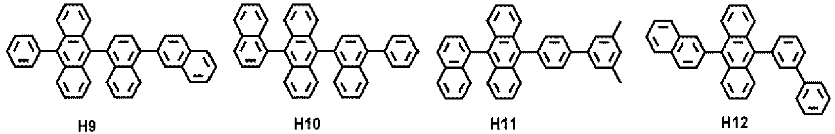


- In an embodiment, the phosphorescent dopant may include at least one transition metal as a central metal.
- The phosphorescent dopant may include a monodentate ligand, a bidentate ligand, a tridentate ligand, a tetradentate ligand, a pentadentate ligand, a hexadentate ligand, or any combination thereof.
- The phosphorescent dopant may be electrically neutral.
- In one or more embodiments, the phosphorescent dopant may include an organometallic compound represented by Formula 401:
Formula 401 M(L401)xc1(L402)xc2

- In Formulae 401 and 402,
- M may be a transition metal (for example, iridium (Ir), platinum (Pt), palladium (Pd), osmium (Os), titanium (Ti), gold (Au), hafnium (Hf), europium (Eu), terbium (Tb), rhodium (Rh), rhenium (Re), or thulium (Tm)),
- L401 may be a ligand represented by Formula 402, and xc1 may be 1, 2, or 3, wherein, when xc1 is 2 or more, two or more of L401 may be identical to or different from each other,
- L402 may be an organic ligand, and xc2 may be 0, 1, 2, 3, or 4, wherein, when xc2 is 2 or more, two or more of L402 may be identical to or different from each other,
- X401 and X402 may each independently be nitrogen or carbon,
- ring A401 and ring A402 may each independently be a C3-C60 carbocyclic group or a C1-C60 heterocyclic group,
- T401 may be a single bond, *-O-*', *-S-*', *-C(=O)-*', *-N(Q411)-*', *-C(Q411)(Q412)-*', *-C(Q411)=C(Q412)-*', *-C(Q411)=*', or *=C(Q411)=*',
- X403 and X404 may each independently be a chemical bond (for example, a covalent bond or a coordinate bond), O, S, N(Q413), B(Q413), P(Q413), C(Q413)(Q414), or Si(Q413)(Q414),
- Q411 to Q414 may each be the same as described in connection with Q1,
- R401 and R402 may each independently be hydrogen, deuterium, -F, -CI, -Br, -I, a hydroxyl group, a cyano group, a nitro group, a C1-C20 alkyl group unsubstituted or substituted with at least one R10a, a C1-C20 alkoxy group unsubstituted or substituted with at least one R10a, a C3-C60 carbocyclic group unsubstituted or substituted with at least one R10a, a C1-C60 heterocyclic group unsubstituted or substituted with at least one R10a, - Si(Q401)(Q402)(Q403), -N(Q401)(Q402), -B(Q401)(Q402), -C(=O)(Q401), -S(=O)2(Q401), or - P(=O)(Q401)(Q402),
- Q401 to Q403 may each be the same as described in connection with Q1,
- xc11 and xc12 may each independently be an integer from 0 to 10, and
- * and *' in Formula 402 each indicate a binding site to M in Formula 401.
- For example, in Formula 402, i) X401 may be nitrogen, and X402 may be carbon, or ii) each of X401 and X402 may be nitrogen.
- In an embodiment, when xc1 in Formula 401 is 2 or more, two ring A401(s) among two or more of L401 may optionally be linked to each other via T402, which is a linking group, and two ring A402(s) among two or more of L401 may optionally be linked to each other via T403, which is a linking group (see Compounds PD1 to PD4 and PD7). T402 and T403 may each be the same as described in connection with T401.
- In Formula 401, L402 may be an organic ligand. For example, L402 may include a halogen group, a diketone group (for example, an acetylacetonate group), a carboxylic acid group (for example, a picolinate group), -C(=O), an isonitrile group, a -CN group, a phosphorus group (for example, a phosphine group, a phosphite group, and the like), or any combination thereof.
- The phosphorescent dopant may include, for example, one of Compounds PD1 to PD39, or any combination thereof:


- The fluorescent dopant may include an amine group-containing compound, a styryl group-containing compound, or any combination thereof.
- For example, the fluorescent dopant may include a compound represented by Formula 501:

- In Formula 501,
- Ar501, L501 to L503, R501, and R502 may each independently be a C3-C60 carbocyclic group unsubstituted or substituted with at least one R10a or a C1-C60 heterocyclic group unsubstituted or substituted with at least one R10a,
- xd1 to xd3 may each independently be 0, 1, 2, or 3, and
- xd4 may be 1, 2, 3, 4, 5, or 6.
- For example, Ar501 in Formula 501 may be a condensed cyclic group (for example, an anthracene group, a chrysene group, a pyrene group, and the like) in which three or more monocyclic groups are condensed together.
- For example, xd4 in Formula 501 may be 2.
- In one or more embodiments, the fluorescent dopant may include: one of Compounds FD1 to FD36; DPVBi; DPAVBi; or any combination thereof:


- The emission layer may include a delayed fluorescence material.
- In the present specification, the delayed fluorescence material may be selected from compounds capable of emitting delayed fluorescence by a delayed fluorescence emission mechanism.
- The delayed fluorescence material included in the emission layer may act as a host or a dopant, depending on the type of other materials included in the emission layer.
- In an embodiment, a difference between a triplet energy level (eV) of the delayed fluorescence material and a singlet energy level (eV) of the delayed fluorescence material may be about 0 eV or more and about 0.5 eV or less. When the difference between the triplet energy level (eV) of the delayed fluorescence material and the singlet energy level (eV) of the delayed fluorescence material is satisfied within the ranges above, upconversion from the triplet state to the singlet state of the delayed fluorescence materials may effectively occur, thereby improving luminescence efficiency or the like of the light-emitting
device 10. - For example, the delayed fluorescence material may include: i) a material including at least one electron donor (for example, a π electron-rich C3-C60 cyclic group and the like, such as a carbazole group) and at least one electron acceptor (for example, a sulfoxide group, a cyano group, a π electron-deficient nitrogen-containing C1-C60 cyclic group, and the like); and ii) a material including a C8-C60 polycyclic group in which two or more cyclic groups are condensed while sharing boron (B).
- Examples of the delayed fluorescence material are at least one of Compounds DF1 to DF9:


- The emission layer may include a quantum dot.
- The term "quantum dot" as used herein refers to a crystal of a semiconductor compound, and may include any material capable of emitting light of various emission wavelengths according to the size of the crystal.
- A diameter of the quantum dot may be, for example, in a range of about 1 nm to about 10 nm.
- The quantum dot may be synthesized by a wet chemical process, a metal organic chemical vapor deposition process, a molecular beam epitaxy process, or any process similar thereto.
- The wet chemical process is a method including mixing a precursor material with an organic solvent and then growing a quantum dot particle crystal. When the crystal grows, the organic solvent naturally acts as a dispersant coordinated on the surface of the quantum dot crystal and controls the growth of the crystal so that the growth of quantum dot particles can be controlled through a process which costs lower, and is easier than vapor deposition methods, such as metal organic chemical vapor deposition (MOCVD) or molecular beam epitaxy (MBE),
- The quantum dot may include: a Group II-VI semiconductor compound; a Group III-V semiconductor compound; a Group III-VI semiconductor compound; a Group I-III-VI semiconductor compound; a Group IV-VI semiconductor compound; a Group IV element or compound; or any combination thereof.
- Examples of the Group II-VI semiconductor compound are: a binary compound, such as CdSe, CdTe, ZnS, ZnSe, ZnTe, ZnO, HgS, HgSe, HgTe, MgSe, MgS, and the like; a ternary compound, such as CdSeS, CdSeTe, CdSTe, ZnSeS, ZnSeTe, ZnSTe, HgSeS, HgSeTe, HgSTe, CdZnS, CdZnSe, CdZnTe, CdHgS, CdHgSe, CdHgTe, HgZnS, HgZnSe, HgZnTe, MgZnSe, MgZnS, and the like; a quaternary compound, such as CdZnSeS, CdZnSeTe, CdZnSTe, CdHgSeS, CdHgSeTe, CdHgSTe, HgZnSeS, HgZnSeTe, HgZnSTe, and the like; or any combination thereof.
- Examples of the Group III-V semiconductor compound are: a binary compound, such as GaN, GaP, GaAs, GaSb, AlN, AlP, AlAs, AlSb, InN, InP, InAs, InSb, and the like; a ternary compound, such as GaNP, GaNAs, GaNSb, GaPAs, GaPSb, AlNP, AlNAs, AlNSb, AlPAs, AlPSb, InGaP, InNP, InAlP, InNAs, InNSb, InPAs, InPSb, and the like; a quaternary compound, such as GaAlNP, GaAlNAs, GaAlNSb, GaAlPAs, GaAlPSb, GaInNP, GaInNAs, GaInNSb, GaInPAs, GaInPSb, InAlNP, InAlNAs, InAlNSb, InAlPAs, InAlPSb, and the like; or any combination thereof. The Group III-V semiconductor compound may further include a Group II element. Examples of the Groups III-V semiconductor compound further including a Group II element are InZnP, InGaZnP, InAIZnP, and the like
- Examples of the Group III-VI semiconductor compound are: a binary compound, such as GaS, GaSe, Ga2Se3, GaTe, InS, InSe, In2S3, In2Se3, InTe, and the like; a ternary compound, such as InGaS3, InGaSe3, and the like; or any combination thereof.
- Examples of the Group I-III-VI semiconductor compound are: a ternary compound, such as AglnS, AgInS2, CulnS, CuInS2, CuGaO2, AgGaO2, AgAlO2, and the like; or any combination thereof.
- Examples of the Group IV-VI semiconductor compound are: a binary compound, such as SnS, SnSe, SnTe, PbS, PbSe, PbTe, and the like; a ternary compound, such as SnSeS, SnSeTe, SnSTe, PbSeS, PbSeTe, PbSTe, SnPbS, SnPbSe, SnPbTe, and the like; a quaternary compound, such as SnPbSSe, SnPbSeTe, SnPbSTe, and the like; or any combination thereof.
- The Group IV element or compound may include: a single element compound, such as Si, Ge, and the like; a binary compound, such as SiC, SiGe, and the like; or any combination thereof.
- Each element included in a multi-element compound, such as the binary compound, the ternary compound, and the quaternary compound, may exist in a particle thereof at a uniform concentration or non-uniform concentration.
- The quantum dot may have a single structure or a dual core-shell structure. In the case of the quantum dot having a single structure, a concentration of each element included in the corresponding quantum dot may be uniform. For example, a material included in the core and a material included in the shell may be different from each other.
- The shell of the quantum dot may act as a protective layer that prevents chemical degeneration of the core to maintain semiconductor characteristics, and/or as a charging layer that imparts electrophoretic characteristics to the quantum dot. The shell may be a single layer or a multi-layer. The interface between the core and the shell may have a concentration gradient in which the concentration of an element existing in the shell decreases toward the center of the core.
- Examples of the shell of the quantum dot are oxide of metal, metalloid, or non-metal, a semiconductor compound, or any combination thereof. Examples of the oxide of metal, metalloid, or non-metal are: a binary compound, such as SiO2, Al2O3, TiO2, ZnO, MnO, Mn2O3, Mn3O4, CuO, FeO, Fe2O3, Fe3O4, CoO, Co3O4, NiO, and the like; a ternary compound, such as MgAl2O4, CoFe2O4, NiFe2O4, CoMn2O4, and the like; or any combination thereof. Examples of the semiconductor compound are: as described herein, a Group II-VI semiconductor compound; a Group III-V semiconductor compound; a Group III-VI semiconductor compound; a Group I-III-VI semiconductor compound; a Group IV-VI semiconductor compound; or any combination thereof. Examples of the semiconductor compound are CdS, CdSe, CdTe, ZnS, ZnSe, ZnTe, ZnSeS, ZnTeS, GaAs, GaP, GaSb, HgS, HgSe, HgTe, InAs, InP, InGaP, InSb, AlAs, AIP, AISb, or any combination thereof.
- A full width of half maximum (FWHM) of an emission wavelength spectrum of the quantum dot may be about 45 nm or less, for example, about 40 nm or less, for example, about 30 nm or less, and within these ranges, color purity or color reproducibility may be increased. In addition, since the light emitted through the quantum dot is emitted in all directions, the wide viewing angle may be improved.
- In addition, the quantum dot may be specifically, spherical, pyramidal, multi-arm, or cubic nanoparticles, nanotubes, nanowires, nanofibers, or nanoplate particles.
- Since the energy band gap may be adjusted by controlling the size of the quantum dot, light having various wavelength bands may be obtained from the emission layer including the quantum dot. Accordingly, by using quantum dot of different sizes, a light-emitting device that emits light of various wavelengths may be implemented. In detail, the size of the quantum dot may be selected in consideration of emitting red light, green light, and/or blue light. In addition, the size of the quantum dot may be configured to emit white light by combination of light of various colors.
- The electron transport region may have: i) a single-layered structure consisting of a single layer consisting of a single material, ii) a single-layered structure consisting of a single layer consisting of a plurality of different materials, or iii) a multi-layered structure including a plurality of layers including different materials.
- The electron-transporting region may include a buffer layer, a hole blocking layer, an electron control layer, an electron transport layer, an electron injection layer, or any combination thereof.
- For example, the electron transport region may have an electron transport layer/electron injection layer structure, a hole blocking layer/electron transport layer/electron injection layer structure, an electron control layer/electron transport layer/electron injection layer structure, or a buffer layer/electron transport layer/electron injection layer structure, wherein constituent layers of each structure are sequentially stacked from the emission layer.
- The electron transport region (for example, the buffer layer, the hole blocking layer, the electron control layer, or the electron transport layer in the electron transport region) may include a metal-free compound including at least one π electron-deficient nitrogen-containing C1-C60 cyclic group.
- For example, the electron transport region may include a compound represented by Formula 601:
Formula 601 [Ar601]xe11-[(L601)xe1-R601]xe21
wherein, in Formula 601, - Ar601 and L601 may each independently be a C3-C60 carbocyclic group unsubstituted or substituted with at least one R10a or a C1-C60 heterocyclic group unsubstituted or substituted with at least one R10a,
- xe11 may be 1, 2, or 3,
- xe1 may be 0, 1, 2, 3, 4, or 5,
- R601 may be a C3-C60 carbocyclic group unsubstituted or substituted with at least one R10a, a C1-C60 heterocyclic group unsubstituted or substituted with at least one R10a, -Si(Q601)(Q602)(Q603), -C(=O)(Q601), -S(=O)2(Q601), or -P(=O)(Q601)(Q602),
- Q601 to Q603 may each be the same as described in connection with Q1,
- xe21 may be 1, 2, 3, 4, or 5, and
- at least one of Ar601, L601, and R601 may each independently be a π electron-deficient nitrogen-containing C1-C60 cyclic group unsubstituted or substituted with at least one R10a.
- In an embodiment, when xe11 in Formula 601 is 2 or more, two or more of Ar601 may be linked together via a single bond.
- In one or more embodiments, Ar601 in Formula 601 may be a substituted or unsubstituted anthracene group.
- In one or more embodiments, the electron transport region may include a compound represented by Formula 601-1:

- In Formula 601-1,
- X614 may be N or C(R614), X615 may be N or C(R615), X616 may be N or C(R616), and at least one of X614 to X616 may be N,
- L611 to L613 may each be the same as described in connection with L601,
- xe611 to xe613 may each be the same as described in connection with xe1,
- R611 to R613 may each be the same as described in connection with R601, and
- R614 to R616 may each independently be hydrogen, deuterium, -F, -CI, -Br, -I, a hydroxyl group, a cyano group, a nitro group, a C1-C20 alkyl group, a C1-C20 alkoxy group, a C3-C60 carbocyclic group unsubstituted or substituted with at least one R10a, or a C1-C60 heterocyclic group unsubstituted or substituted with at least one R10a.
- For example, xe1 and xe611 to xe613 in Formulae 601 and 601-1 may each independently be 0, 1, or 2.
- In one or more embodiments, the electron transport region may include one of Compounds ET1 to ET45, 2,9-dimethyl-4,7-diphenyl-1,10-phenanthroline (BCP), 4,7-diphenyl-1,10-phenanthroline (Bphen), Alq3, BAlq, TAZ, NTAZ, or any combination thereof:


- A thickness of the electron transport region may be in a range of about 100 Å to about 5,000 Å, for example, about 160 Å to about 4,000 Å. When the electron transport region includes a buffer layer, a hole blocking layer, an electron control layer, an electron transport layer, or any combination thereof, a thickness of the buffer layer, the hole blocking layer, or the electron control layer may be in a range of about 20 Å to about 1,000 Å, for example, about 30 Å to about 300 Å, and a thickness of the electron transport layer may be un a range of about 100 Å to about 1,000 Å, for example, about 150 Å to about 500 Å. When the thicknesses of the buffer layer, the hole blocking layer, the electron control layer, the electron transport layer, and/or the electron transport layer are within these ranges, satisfactory electron transporting characteristics may be obtained without a substantial increase in driving voltage.
- The electron transport region (for example, the electron transport layer in the electron transport region) may further include, in addition to the materials described above, a metal-containing material.
- The metal-containing material may include an alkali metal complex, an alkaline earth metal complex, or any combination thereof. The metal ion of an alkali metal complex may be a Li ion, a Na ion, a K ion, a Rb ion, or a Cs ion, and the metal ion of an alkaline earth metal complex may be a Be ion, a Mg ion, a Ca ion, a Sr ion, or a Ba ion. A ligand coordinated with the metal ion of the alkali metal complex or the alkaline earth-metal complex may include a hydroxyquinoline, a hydroxyisoquinoline, a hydroxybenzoquinoline, a hydroxyacridine, a hydroxyphenanthridine, a hydroxyphenyloxazole, a hydroxyphenylthiazole, a hydroxyphenyloxadiazole, a hydroxyphenylthiadiazole, a hydroxyphenylpyridine, a hydroxyphenylbenzimidazole, a hydroxyphenylbenzothiazole, a bipyridine, a phenanthroline, a cyclopentadiene, or any combination thereof.
- For example, the metal-containing material may include a Li complex. The Li complex may include, for example, Compound ET-D1 (LiQ) or ET-D2:

- The electron transport region may include an electron injection layer that facilitates the injection of electrons from the
second electrode 150. The electron injection layer may directly contact thesecond electrode 150. - The electron injection layer may have: i) a single-layered structure consisting of a single layer consisting of a single material, ii) a single-layered structure consisting of a single layer consisting of a plurality of different materials, or iii) a multi-layered structure including a plurality of layers including different materials.
- The electron injection layer may include an alkali metal, alkaline earth metal, a rare earth metal, an alkali metal-containing compound, alkaline earth metal-containing compound, a rare earth metal-containing compound, an alkali metal complex, an alkaline earth metal complex, a rare earth metal complex, or any combination thereof.
- The alkali metal may include Li, Na, K, Rb, Cs, or any combination thereof. The alkaline earth metal may include Mg, Ca, Sr, Ba, or any combination thereof. The rare earth metal may include Sc, Y, Ce, Tb, Yb, Gd, or any combination thereof.
- The alkali metal-containing compound, the alkaline earth metal-containing compound, and the rare earth metal-containing compound may be oxides, halides (for example, fluorides, chlorides, bromides, iodides, and the like), or tellurides of the alkali metal, the alkaline earth metal, and the rare earth metal, or any combination thereof.
- The alkali metal-containing compound may include alkali metal oxides, such as Li2O, Cs2O, K2O, and the like, alkali metal halides, such as LiF, NaF, CsF, KF, Lil, Nal, Csl, KI, and the like, or any combination thereof. The alkaline earth metal-containing compound may include an alkaline earth metal compound, such as BaO, SrO, CaO, BaxSr1-xO (wherein x is a real number satisfying the condition of 0<x<1), BaxCai-xO (wherein x is a real number satisfying the condition of 0<x<1), or the like. The rare earth metal-containing compound may include YbF3, ScF3, Sc2O3, Y2O3, Ce2O3, GdF3, TbF3, YbI3, ScI3, TbI3, or any combination thereof. For example, the rare earth metal-containing compound may include lanthanide metal telluride. Examples of the lanthanide metal telluride are LaTe, CeTe, PrTe, NdTe, PmTe, SmTe, EuTe, GdTe, TbTe, DyTe, HoTe, ErTe, TmTe, YbTe, LuTe, La2Te3, Ce2Te3, Pr2Te3, Nd2Te3, Pm2Te3, Sm2Te3, Eu2Te3, Gd2Te3, Tb2Te3, Dy2Te3, Ho2Te3, Er2Te3, Tm2Te3, Yb2Te3, Lu2Te3, and the like.
- The alkali metal complex, the alkaline earth-metal complex, and the rare earth metal complex may include: i) one of ions of the alkali metal, the alkaline earth metal, and the rare earth metal; and ii), as a ligand linked to the metal ion, for example, hydroxyquinoline, hydroxyisoquinoline, hydroxybenzoquinoline, hydroxyacridine, hydroxyphenanthridine, hydroxyphenyloxazole, hydroxyphenylthiazole, hydroxyphenyloxadiazole, hydroxyphenylthiadiazole, hydroxyphenylpyridine, hydroxyphenyl benzimidazole, hydroxyphenylbenzothiazole, bipyridine, phenanthroline, cyclopentadiene, or any combination thereof.
- In an embodiment, the electron injection layer may consist of an alkali metal, an alkaline earth metal, a rare earth metal, an alkali metal-containing compound, an alkaline earth metal-containing compound, a rare earth metal-containing compound, an alkali metal complex, an alkaline earth metal complex, a rare earth metal complex, or any combination thereof, as described above. In one or more embodiments, the electron injection layer may further include an organic material (for example, the compound represented by Formula 601).
- In one or more embodiments, the electron injection layer may consist of: i) an alkali metal-containing compound (for example, an alkali metal halide); or ii) a) an alkali metal-containing compound (for example, an alkali metal halide), and b) an alkali metal, an alkaline earth metal, a rare earth metal, or any combination thereof. In one or more embodiments, the electron injection layer may be a KI:Yb co-deposited layer, an RbI:Yb co-deposited layer, and the like.
- When the electron injection layer further includes an organic material, alkali metal, alkaline earth metal, rare earth metal, an alkali metal-containing compound, an alkaline earth metal-containing compound, a rare earth metal-containing compound, alkali metal complex, alkaline earth-metal complex, rare earth metal complex, or any combination thereof may be uniformly or non-uniformly dispersed in a matrix including the organic material.
- A thickness of the electron injection layer may be in a range of about 1 Å to about 100 Å, for example, about 3 Å to about 90 Å. When the thickness of the electron injection layer is within these ranges, satisfactory electron injection characteristics may be obtained without a substantial increase in driving voltage.
- The
second electrode 150 may be located on theinterlayer 130 having a structure as described above. Thesecond electrode 150 may be a cathode, which is an electron injection electrode, and as the material for thesecond electrode 150, a metal, an alloy, an electrically conductive compound, or any combination thereof, each having a low-work function, may be used. - The
second electrode 150 may include lithium (Li), silver (Ag), magnesium (Mg), aluminum (Al), aluminum-lithium (Al-Li), calcium (Ca), magnesium-indium (Mg-In), magnesium-silver (Mg-Ag), ytterbium (Yb), silver-ytterbium (Ag-Yb), ITO, IZO, or any combination thereof. Thesecond electrode 150 may be a transmissive electrode, a semi-transmissive electrode, or a reflective electrode. - The
second electrode 150 may have a single-layered structure or a multi-layered structure including a plurality of layers. - A first capping layer may be located outside the
first electrode 110, and/or a second capping layer may be located outside thesecond electrode 150. In particular, the light-emittingdevice 10 may have a structure in which the first capping layer, thefirst electrode 110, theinterlayer 130, and thesecond electrode 150 are sequentially stacked in the stated order, a structure in which thefirst electrode 110, theinterlayer 130, thesecond electrode 150, and the second capping layer are sequentially stacked in the stated order, or a structure in which the first capping layer, thefirst electrode 110, theinterlayer 130, thesecond electrode 150, and the second capping layer are sequentially stacked in the stated order. - Light generated in the emission layer of the
interlayer 130 of the light-emittingdevice 10 may be extracted toward the outside through thefirst electrode 110 which is a semi-transmissive electrode or a transmissive electrode, and the first capping layer. Light generated in the emission layer of theinterlayer 130 of the light-emittingdevice 10 may be extracted toward the outside through thesecond electrode 150 which is a semi-transmissive electrode or a transmissive electrode, and the second capping layer. - The first capping layer and the second capping layer may increase external emission efficiency according to the principle of constructive interference. Accordingly, the light extraction efficiency of the light-emitting
device 10 is increased, so that the luminescence efficiency of the light-emittingdevice 10 may be improved. - Each of the first capping layer and the second capping layer may include a material having a refractive index of 1.6 or more (at 589 nm).
- The first capping layer and the second capping layer may each independently be an organic capping layer including an organic material, an inorganic capping layer including an inorganic material, or an organic-inorganic composite capping layer including an organic material and an inorganic material.
- In an embodiment, at least one of the first capping layer and the second capping layer may each independently include a carbocyclic compound, a heterocyclic compound, an amine group-containing compound, a porphine derivative, a phthalocyanine derivative, a naphthalocyanine derivative, an alkali metal complex, an alkaline earth metal complex, or any combination thereof. The carbocyclic compound, the heterocyclic compound, and the amine group-containing compound may each optionally be substituted with a substituent including O, N, S, Se, Si, F, Cl, Br, I, or any combination thereof. In one or more embodiments, at least one of the first capping layer and the second capping layer may each independently include an amine group-containing compound.
- In one or more embodiments, at least one of the first capping layer and the second capping layer may each independently include a compound represented by Formula 201, a compound represented by Formula 202, or any combination thereof.
- In one or more embodiments, at least one of the first capping layer and the second capping layer may each independently include one of Compounds HT28 to HT33, one of Compounds CP1 to CP6, β-NPB, or any combination thereof:


- The heterocyclic compound represented by Formula 1 may be included in various films. Accordingly, another aspect of the present disclosure provides a film including the heterocyclic compound represented by Formula 1. The film may be, for example, an optical member (or a light control means) (for example, a color filter, a color conversion member, a capping layer, a light extraction efficiency enhancement layer, a selective light absorbing layer, a polarizing layer, a quantum dot-containing layer, or like), a lightblocking member (for example, a light reflective layer, a light absorbing layer, or the like), a protective member (for example, an insulating layer, a dielectric layer, or the like).
- The light-emitting device may be included in various electronic apparatuses. For example, an electronic apparatus including the light-emitting device may be a light-emitting apparatus, an authentication apparatus, or the like.
- The electronic apparatus (for example, a light-emitting apparatus) may further include, in addition to the light-emitting device, i) a color filter, ii) a color conversion layer, or iii) a color filter and a color conversion layer. The color filter and/or the color conversion layer may be located in at least one traveling direction of light emitted from the light-emitting device. For example, light emitted from the light-emitting device may be blue light or white light. Details for the light-emitting device may be the same as described herein. In an embodiment, the color conversion layer may include a quantum dot. The quantum dots may be, for example, the same as described herein.
- The electronic apparatus may include a first substrate. The first substrate may include a plurality of subpixel areas, the color filter may include a plurality of color filter areas respectively corresponding to the subpixel areas, and the color conversion layer may include a plurality of color conversion areas respectively corresponding to the subpixel areas.
- A pixel-defining film may be located among the subpixel areas to define each of the subpixel areas.
- The color filter may further include a plurality of color filter areas and light-shielding patterns located among the color filter areas, and the color conversion layer may further include a plurality of color conversion areas and light-shielding patterns located among the color conversion areas.
- The plurality of color filter areas (or the plurality of color conversion areas) may include a first area emitting first color light, a second area emitting second color light, and/or a third area emitting third color light, wherein the first color light, the second color light, and/or the third color light may have different maximum emission wavelengths from one another. For example, the first color light may be red light, the second color light may be green light, and the third color light may be blue light. For example, the plurality of color filter areas (or the plurality of color conversion areas) may include quantum dots. In particular, the first region may include red quantum dots, the second region may include green quantum dots, and the third region may not include quantum dots. Details for the quantum dots are the same as described herein. The first region, the second region, and/or the third region may each include a scatter.
- For example, the light-emitting device may emit first light, the first region may absorb the first light to emit first-first color light, the second region may absorb the first light to emit second-first color light, and the third region may absorb the first light to emit third-first color light. In this regard, the first-first color light, the second-first color light, and the third-first color light may have different maximum emission wavelengths from each other. In particular, the first light may be blue light, the first-first color light may be red light, the second-first color light may be green light, and the third-first color light may be blue light.
- The electronic apparatus may further include a thin-film transistor, in addition to the light-emitting device as described above. The thin-film transistor may include a source electrode, a drain electrode, and an activation layer, wherein any one of the source electrode and the drain electrode may be electrically connected to any one of the first electrode and the second electrode of the light-emitting device.
- The thin-film transistor may further include a gate electrode, a gate insulating film, or the like.
- The activation layer may include crystalline silicon, amorphous silicon, an organic semiconductor, an oxide semiconductor, or the like.
- The electronic apparatus may further include a sealing portion for sealing the light-emitting device. The sealing portion may be located between the color conversion layer and/or color filter and the light-emitting device. The sealing portion allows light from the light-emitting device to be extracted to the outside, and simultaneously prevents ambient air and moisture from penetrating into the light-emitting device. The sealing portion may be a sealing substrate including a transparent glass substrate or a plastic substrate. The sealing portion may be a thin-film encapsulation layer including at least one layer of an organic layer and/or an inorganic layer. When the sealing portion is a thin film encapsulation layer, the electronic apparatus may be flexible.
- Various functional layers may be additionally located on the sealing portion, in addition to the color filter and/or the color conversion layer, according to the use of the electronic apparatus. Examples of the functional layers may include a touch screen layer, a polarizing layer, and the like. The touch screen layer may be a pressure-sensitive touch screen layer, a capacitive touch screen layer, or an infrared touch screen layer. The authentication apparatus may be, for example, a biometric authentication apparatus that authenticates an individual by using biometric information of a living body (for example, fingertips, pupils, and the like).
- The authentication apparatus may further include, in addition to the light-emitting device as described above, a biometric information collector.
- The electronic apparatus may be applied to various displays, light sources, lighting, personal computers (for example, a mobile personal computer), mobile phones, digital cameras, electronic organizers, electronic dictionaries, electronic game machines, medical instruments (for example, electronic thermometers, sphygmomanometers, blood glucose meters, pulse measurement devices, pulse wave measurement devices, electrocardiogram displays, ultrasonic diagnostic devices, or endoscope displays), fish finders, various measuring instruments, meters (for example, meters for a vehicle, an aircraft, and a vessel), projectors, and the like.
-
FIG. 2 is a cross-sectional view showing a light-emitting apparatus according to an embodiment of the present disclosure. - The light-emitting apparatus of
FIG. 2 includes asubstrate 100, a thin-film transistor (TFT), a light-emitting device, and anencapsulation portion 300 that seals the light-emitting device. - The
substrate 100 may be a flexible substrate, a glass substrate, or a metal substrate. Abuffer layer 210 may be located on thesubstrate 100. Thebuffer layer 210 may prevent penetration of impurities through thesubstrate 100 and may provide a flat surface on thesubstrate 100. - A TFT may be located on the
buffer layer 210. The TFT may include anactivation layer 220, agate electrode 240, asource electrode 260, and adrain electrode 270. - The
activation layer 220 may include an inorganic semiconductor such as silicon or polysilicon, an organic semiconductor, or an oxide semiconductor, and may include a source region, a drain region, and a channel region. - A
gate insulating film 230 for insulating theactivation layer 220 from thegate electrode 240 may be located on theactivation layer 220, and thegate electrode 240 may be located on thegate insulating film 230. - An interlayer insulating
film 250 may be located on thegate electrode 240. Theinterlayer insulating film 250 may be located between thegate electrode 240 and thesource electrode 260 and between thegate electrode 240 and thedrain electrode 270, to insulate from one another. - The
source electrode 260 and thedrain electrode 270 may be located on theinterlayer insulating film 250. Theinterlayer insulating film 250 and thegate insulating film 230 may be formed to expose the source region and the drain region of theactivation layer 220, and thesource electrode 260 and thedrain electrode 270 may be located in contact with the exposed portions of the source region and the drain region of theactivation layer 220. - The TFT is electrically connected to a light-emitting device to drive the light-emitting device, and is covered and protected by a
passivation layer 280. Thepassivation layer 280 may include an inorganic insulating film, an organic insulating film, or any combination thereof. A light-emitting device is provided on thepassivation layer 280. The light-emitting device may include afirst electrode 110, aninterlayer 130, and asecond electrode 150. - The
first electrode 110 may be located on thepassivation layer 280. Thepassivation layer 280 may be located to expose a portion of thedrain electrode 270, not fully covering thedrain electrode 270, and thefirst electrode 110 may be located to be connected to the exposed portion of thedrain electrode 270. - A
pixel defining layer 290 including an insulating material may be located on thefirst electrode 110. Thepixel defining layer 290 may expose a certain region of thefirst electrode 110, and aninterlayer 130 may be formed in the exposed region of thefirst electrode 110. Thepixel defining layer 290 may be a polyimide or polyacrylic organic film. Although not shown inFIG. 2 , at least some layers of theinterlayer 130 may extend beyond the upper portion of thepixel defining layer 290 to be located in the form of a common layer. - The
second electrode 150 may be located on theinterlayer 130, and acapping layer 170 may be additionally formed on thesecond electrode 150. Thecapping layer 170 may be formed to cover thesecond electrode 150. - The
encapsulation portion 300 may be located on thecapping layer 170. Theencapsulation portion 300 may be located on a light-emitting device to protect the light-emitting device from moisture or oxygen. Theencapsulation portion 300 may include: an inorganic film including silicon nitride (SiNx), silicon oxide (SiOx), indium tin oxide, indium zinc oxide, or any combination thereof; an organic film including polyethylene terephthalate, polyethylene naphthalate, polycarbonate, polyimide, polyethylene sulfonate, polyoxymethylene, polyarylate, hexamethyldisiloxane, an acrylic resin (for example, polymethyl methacrylate, polyacrylic acid, and the like), an epoxy-based resin (for example, aliphatic glycidyl ether (AGE), and the like), or any combination thereof; or any combination of the inorganic films and the organic films. -
FIG. 3 shows a cross-sectional view showing a light-emitting apparatus according to an embodiment of the present disclosure. - The light-emitting apparatus of
FIG. 3 is the same as the light-emitting apparatus ofFIG. 2 , except that a light-shielding pattern 500 and afunctional region 400 are additionally located on theencapsulation portion 300. Thefunctional region 400 may be i) a color filter area, ii) a color conversion area, or iii) a combination of the color filter area and the color conversion area. In an embodiment, the light-emitting device included in the light-emitting apparatus ofFIG. 3 may be a tandem light-emitting device. - The layers included in the hole transport region, the emission layer, and the layers included in the electron transport region may be formed in a certain region by using various methods such as vacuum deposition, spin coating, casting, Langmuir-Blodgett (LB) deposition, ink-jet printing, laser-printing, laser-induced thermal imaging, and the like.
- When layers constituting the hole transport region, an emission layer, and layers constituting the electron transport region are formed by vacuum deposition, the deposition may be performed at a deposition temperature of about 100 °C to about 500 °C, a vacuum degree of about 10-8 torr to about 10-3 torr, and a deposition speed of about 0.01 Å/sec to about 100 Å/sec, depending on a material to be included in a layer to be formed and the structure of a layer to be formed.
- The term "C3-C60 carbocyclic group" as used herein refers to a cyclic group consisting of carbon only as a ring-forming atom and having three to sixty carbon atoms, and the term "C1-C60 heterocyclic group" as used herein refers to a cyclic group that has one to sixty carbon atoms and further has, in addition to carbon, a heteroatom as a ring-forming atom. The C3-C60 carbocyclic group and the C1-C60 heterocyclic group may each be a monocyclic group consisting of one ring or a polycyclic group in which two or more rings are condensed with each other. For example, the C1-C60 heterocyclic group has 3 to 61 ring-forming atoms.
- The "cyclic group" as used herein may include the C3-C60 carbocyclic group, and the C1-C60 heterocyclic group.
- The term "π electron-rich C3-C60 cyclic group" as used herein refers to a cyclic group that has three to sixty carbon atoms and does not include *-N=*' as a ring-forming moiety, and the term "π electron-deficient nitrogen-containing C1-C60 cyclic group" as used herein refers to a heterocyclic group that has one to sixty carbon atoms and includes *-N=*' as a ring-forming moiety.
- For example,
- the C3-C60 carbocyclic group may be i) a T1 group or ii) a condensed cyclic group in which two or more T1 groups are condensed with each other (for example, a cyclopentadiene group, an adamantane group, a norbornane group, a benzene group, a pentalene group, a naphthalene group, an azulene group, an indacene group, an acenaphthylene group, a phenalene group, a phenanthrene group, an anthracene group, a fluoranthene group, a triphenylene group, a pyrene group, a chrysene group, a perylene group, a pentaphene group, a heptalene group, a naphthacene group, a picene group, a hexacene group, a pentacene group, a rubicene group, a coronene group, an ovalene group, an indene group, a fluorene group, a spiro-bifluorene group, a benzofluorene group, an indenophenanthrene group, or an indenoanthracene group),
- the C1-C60 heterocyclic group may be i) a T2 group, ii) a condensed cyclic group in which two or more T2 groups are condensed with each other, or iii) a condensed cyclic group in which at least one T2 group and at least one T1 group are condensed with each other (for example, a pyrrole group, a thiophene group, a furan group, an indole group, a benzoindole group, a naphthoindole group, an isoindole group, a benzoisoindole group, a naphthoisoindole group, a benzosilole group, a benzothiophene group, a benzofuran group, a carbazole group, a dibenzosilole group, a dibenzothiophene group, a dibenzofuran group, an indenocarbazole group, an indolocarbazole group, a benzofurocarbazole group, a benzothienocarbazole group, a benzosilolocarbazole group, a benzoindolocarbazole group, a benzocarbazole group, a benzonaphthofuran group, a benzonaphthothiophene group, a benzonaphthosilole group, a benzofurodibenzofuran group, a benzofurodibenzothiophene group, a benzothienodibenzothiophene group, a pyrazole group, an imidazole group, a triazole group, an oxazole group, an isoxazole group, an oxadiazole group, a thiazole group, an isothiazole group, a thiadiazole group, a benzopyrazole group, a benzimidazole group, a benzoxazole group, a benzoisoxazole group, a benzothiazole group, a benzoisothiazole group, a pyridine group, a pyrimidine group, a pyrazine group, a pyridazine group, a triazine group, a quinoline group, an isoquinoline group, a benzoquinoline group, a benzoisoquinoline group, a quinoxaline group, a benzoquinoxaline group, a quinazoline group, a benzoquinazoline group, a phenanthroline group, a cinnoline group, a phthalazine group, a naphthyridine group, an imidazopyridine group, an imidazopyrimidine group, an imidazotriazine group, an imidazopyrazine group, an imidazopyridazine group, an azacarbazole group, an azafluorene group, an azadibenzosilole group, an azadibenzothiophene group, an azadibenzofuran group, and the like),
- the π electron-rich C3-C60 cyclic group may be i) a T1 group, ii) a condensed cyclic group in which two or more T1 groups are condensed with each other, iii) a T3 group, iv) a condensed cyclic group in which two or more T3 groups are condensed with each other, or v) a condensed cyclic group in which at least one T3 group and at least one T1 group are condensed with each other (for example, the C3-C60 carbocyclic group, a 1H-pyrrole group, a silole group, a borole group, a 2H-pyrrole group, a 3H-pyrrole group, a thiophene group, a furan group, an indole group, a benzoindole group, a naphthoindole group, an isoindole group, a benzoisoindole group, a naphthoisoindole group, a benzosilole group, a benzothiophene group, a benzofuran group, a carbazole group, a dibenzosilole group, a dibenzothiophene group, a dibenzofuran group, an indenocarbazole group, an indolocarbazole group, a benzofurocarbazole group, a benzothienocarbazole group, a benzosilolocarbazole group, a benzoindolocarbazole group, a benzocarbazole group, a benzonaphthofuran group, a benzonaphthothiophene group, a benzonaphthosilole group, a benzofurodibenzofuran group, a benzofurodibenzothiophene group, a benzothienodibenzothiophene group, and the like),
- the π electron-deficient nitrogen-containing C1-C60 cyclic group may be i) a T4 group, ii) a condensed cyclic group in which two or more T4 groups are condensed with each other, iii) a condensed cyclic group in which at least one T4 group and at least one T1 group are condensed with each other, iv) a condensed cyclic group in which at least one T4 group and at least one T3 group are condensed with each other, or v) a condensed cyclic group in which at least one T4 group, at least one T1 group, and at least one T3 group are condensed with one another (for example, a pyrazole group, an imidazole group, a triazole group, an oxazole group, an isoxazole group, an oxadiazole group, a thiazole group, an isothiazole group, a thiadiazole group, a benzopyrazole group, a benzimidazole group, a benzoxazole group, a benzoisoxazole group, a benzothiazole group, a benzoisothiazole group, a pyridine group, a pyrimidine group, a pyrazine group, a pyridazine group, a triazine group, a quinoline group, an isoquinoline group, a benzoquinoline group, a benzoisoquinoline group, a quinoxaline group, a benzoquinoxaline group, a quinazoline group, a benzoquinazoline group, a phenanthroline group, a cinnoline group, a phthalazine group, a naphthyridine group, an imidazopyridine group, an imidazopyrimidine group, an imidazotriazine group, an imidazopyrazine group, an imidazopyridazine group, an azacarbazole group, an azafluorene group, an azadibenzosilole group, an azadibenzothiophene group, an azadibenzofuran group, and the like),
- the T1 group may be a cyclopropane group, a cyclobutane group, a cyclopentane group, a cyclohexane group, a cycloheptane group, a cyclooctane group, a cyclobutene group, a cyclopentene group, a cyclopentadiene group, a cyclohexene group, a cyclohexadiene group, a cycloheptene group, an adamantane group, a norbornane (or a bicyclo[2.2.1]heptane) group, a norbornene group, a bicyclo[1.1.1]pentane group, a bicyclo[2.1.1]hexane group, a bicyclo[2.2.2]octane group, or a benzene group,
- the T2 group may be a furan group, a thiophene group, a 1H-pyrrole group, a silole group, a borole group, a 2H-pyrrole group, a 3H-pyrrole group, an imidazole group, a pyrazole group, a triazole group, a tetrazole group, an oxazole group, an isoxazole group, an oxadiazole group, a thiazole group, an isothiazole group, a thiadiazole group, an azasilole group, an azaborole group, a pyridine group, a pyrimidine group, a pyrazine group, a pyridazine group, a triazine group, a tetrazine group, a pyrrolidine group, an imidazolidine group, a dihydropyrrole group, a piperidine group, a tetrahydropyridine group, a dihydropyridine group, a hexahydropyrimidine group, a tetrahydropyrimidine group, a dihydropyrimidine group, a piperazine group, a tetrahydropyrazine group, a dihydropyrazine group, a tetrahydropyridazine group, or a dihydropyridazine group,
- the T3 group may be a furan group, a thiophene group, a 1H-pyrrole group, a silole group, or a borole group, and
- the T4 group may be a 2H-pyrrole group, a 3H-pyrrole group, an imidazole group, a pyrazole group, a triazole group, a tetrazole group, an oxazole group, an isoxazole group, an oxadiazole group, a thiazole group, an isothiazole group, a thiadiazole group, an azasilole group, an azaborole group, a pyridine group, a pyrimidine group, a pyrazine group, a pyridazine group, a triazine group, or a tetrazine group.
- The terms "the cyclic group, the C3-C60 carbocyclic group, the C1-C60 heterocyclic group, the π electron-rich C3-C60 cyclic group, or the π electron-deficient nitrogen-containing C1-C60 cyclic group" as used herein refer to a group condensed to any cyclic group, a monovalent group, or a polyvalent group (for example, a divalent group, a trivalent group, a tetravalent group, and the like) according to the structure of a formula for which the corresponding term is used. For example, the "benzene group" may be a benzo group, a phenyl group, a phenylene group, or the like, which may be easily understood by one of ordinary skill in the art according to the structure of a formula including the "benzene group."
- Examples of the monovalent C3-C60 carbocyclic group and the monovalent C1-C60 heterocyclic group are a C3-C10 cycloalkyl group, a C1-C10 heterocycloalkyl group, a C3-C10 cycloalkenyl group, a C1-C10 heterocycloalkenyl group, a C6-C60 aryl group, a C1-C60 heteroaryl group, a monovalent non-aromatic condensed polycyclic group, and a monovalent non-aromatic condensed heteropolycyclic group. Examples of the divalent C3-C60 carbocyclic group and the monovalent C1-C60 heterocyclic group are a C3-C10 cycloalkylene group, a C1-C10 heterocycloalkylene group, a C3-C10 cycloalkenylene group, a C1-C10 heterocycloalkenylene group, a C6-C60 arylene group, a C1-C60 heteroarylene group, a divalent non-aromatic condensed polycyclic group, and a substituted or unsubstituted divalent non-aromatic condensed heteropolycyclic group.
- The term "C1-C60 alkyl group" as used herein refers to a linear or branched aliphatic hydrocarbon monovalent group that has one to sixty carbon atoms, and specific examples thereof are a methyl group, an ethyl group, an n-propyl group, an isopropyl group, an n-butyl group, a sec-butyl group, an isobutyl group, a tert-butyl group, an n-pentyl group, a tert-pentyl group, a neopentyl group, an isopentyl group, a sec-pentyl group, a 3-pentyl group, a sec-isopentyl group, an n-hexyl group, an isohexyl group, a sec-hexyl group, a tert-hexyl group, an n-heptyl group, an isoheptyl group, a sec-heptyl group, a tert-heptyl group, an n-octyl group, an isooctyl group, a sec-octyl group, a tert-octyl group, an n-nonyl group, an isononyl group, a sec-nonyl group, a tert-nonyl group, an n-decyl group, an isodecyl group, a sec-decyl group, a tert-decyl group, and the like. The term "C1-C60 alkylene group" as used herein refers to a divalent group having the same structure as the C1-C60 alkyl group.
- The term "C2-C60 alkenyl group" as used herein refers to a monovalent hydrocarbon group having at least one carbon-carbon double bond in the middle or at the terminus of the C2-C60 alkyl group, and examples thereof are an ethenyl group, a propenyl group, a butenyl group, and the like. The term "C2-C60 alkenylene group" as used herein refers to a divalent group having the same structure as the C2-C60 alkenyl group.
- The term "C2-C60 alkynyl group" as used herein refers to a monovalent hydrocarbon group having at least one carbon-carbon triple bond in the middle or at the terminus of the C2-C60 alkyl group, and examples thereof are an ethynyl group, a propynyl group, and the like. The term "C2-C60 alkynylene group" as used herein refers to a divalent group having the same structure as the C2-C60 alkynyl group.
- The term "C1-C60 alkoxy group" as used herein refers to a monovalent group represented by -OA101 (wherein A101 is the C1-C60 alkyl group), and examples thereof are a methoxy group, an ethoxy group, an isopropyloxy group, and the like.
- The term "C3-C10 cycloalkyl group" as used herein refers to a monovalent saturated hydrocarbon cyclic group having 3 to 10 carbon atoms, and examples thereof are a cyclopropyl group, a cyclobutyl group, a cyclopentyl group, a cyclohexyl group, a cycloheptyl group, a cyclooctyl group, an adamantanyl group, a norbornanyl group (or bicyclo[2.2.1]heptyl group), a bicyclo[1.1.1]pentyl group, a bicyclo[2.1.1]hexyl group, a bicyclo[2.2.2]octyl group, and the like. The term "C3-C10 cycloalkylene group" as used herein refers to a divalent group having the same structure as the C3-C10 cycloalkyl group.
- The term "C1-C10 heterocycloalkyl group" as used herein refers to a monovalent cyclic group of 1 to 10 carbon atoms, further including, in addition to carbon atoms, at least one heteroatom, as ring-forming atoms, and specific examples are a 1,2,3,4-oxatriazolidinyl group, a tetrahydrofuranyl group, a tetrahydrothiophenyl group, and the like. The term "C1-C10 heterocycloalkylene group" as used herein refers to a divalent group having the same structure as the C1-C10 heterocycloalkyl group.
- The term C3-C10 cycloalkenyl group used herein refers to a monovalent cyclic group that has three to ten carbon atoms and at least one carbon-carbon double bond in the ring thereof and no aromaticity, and specific examples thereof are a cyclopentenyl group, a cyclohexenyl group, a cycloheptenyl group, and the like. The term "C3-C10 cycloalkenylene group" as used herein refers to a divalent group having the same structure as the C3-C10 cycloalkenyl group.
- The term "C1-C10 heterocycloalkenyl group" as used herein refers to a monovalent cyclic group of 1 to 10 carbon atoms, further including, in addition to carbon atoms, at least one heteroatom, as ring-forming atoms, and having at least one carbon-carbon double bond in the cyclic structure thereof. Examples of the C1-C10 heterocycloalkenyl group are a 4,5-dihydro-1,2,3,4-oxatriazolyl group, a 2,3-dihydrofuranyl group, a 2,3-dihydrothiophenyl group, and the like. The term "C1-C10 heterocycloalkenylene group" as used herein refers to a divalent group having the same structure as the C1-C10 heterocycloalkenyl group.
- The term "C6-C60 aryl group" as used herein refers to a monovalent group having a carbocyclic aromatic system of 6 to 60 carbon atoms, and the term "C6-C60 arylene group" as used herein refers to a divalent group having a carbocyclic aromatic system of 6 to 60 carbon atoms. Examples of the C6-C60 aryl group are a phenyl group, a pentalenyl group, a naphthyl group, an azulenyl group, an indacenyl group, an acenaphthyl group, a phenalenyl group, a phenanthrenyl group, an anthracenyl group, a fluoranthenyl group, a triphenylenyl group, a pyrenyl group, a chrysenyl group, a perylenyl group, a pentaphenyl group, a heptalenyl group, a naphthacenyl group, a picenyl group, a hexacenyl group, a pentacenyl group, a rubicenyl group, a coronenyl group, an ovalenyl group, and the like. When the C6-C60 aryl group and the C6-C60 arylene group each include two or more rings, the two or more rings may be condensed with each other.
- The term "C1-C60 heteroaryl group" as used herein refers to a monovalent group having a heterocyclic aromatic system of 1 to 60 carbon atoms, further including, in addition to carbon atoms, at least one heteroatom, as ring-forming atoms. The term "C1-C60 heteroarylene group" as used herein refers to a divalent group having a heterocyclic aromatic system of 1 to 60 carbon atoms, further including, in addition to carbon atoms, at least one heteroatom, as ring-forming atoms. Examples of the C1-C60 heteroaryl group are a pyridinyl group, a pyrimidinyl group, a pyrazinyl group, a pyridazinyl group, a triazinyl group, a quinolinyl group, a benzoquinolinyl group, an isoquinolinyl group, a benzoisoquinolinyl group, a quinoxalinyl group, a benzoquinoxalinyl group, a quinazolinyl group, a benzoquinazolinyl group, a cinnolinyl group, a phenanthrolinyl group, a phthalazinyl group, a naphthyridinyl group, and the like. When the C1-C60 heteroaryl group and the C1-C60 heteroarylene group each include two or more rings, the rings may be condensed with each other.
- The term "monovalent non-aromatic condensed polycyclic group" as used herein refers to a monovalent group (for example, having 8 to 60 carbon atoms) having two or more rings condensed to each other, only carbon atoms as ring-forming atoms, and no aromaticity in its entire molecular structure. Examples of the monovalent non-aromatic condensed polycyclic group are an indenyl group, a fluorenyl group, a spiro-bifluorenyl group, a benzofluorenyl group, an indenophenanthrenyl group, and an indeno anthracenyl group. The term "divalent non-aromatic condensed polycyclic group" as used herein refers to a divalent group having the same structure as the monovalent non-aromatic condensed polycyclic group described above.
- The term "monovalent non-aromatic condensed heteropolycyclic group" as used herein refers to a monovalent group (for example, having 1 to 60 carbon atoms) having two or more rings condensed to each other, further including, in addition to carbon atoms, at least one heteroatom, as ring-forming atoms, and having non-aromaticity in its entire molecular structure. Examples of the monovalent non-aromatic condensed heteropolycyclic group are a pyrrolyl group, a thiophenyl group, a furanyl group, an indolyl group, a benzoindolyl group, a naphthoindolyl group, an isoindolyl group, a benzoisoindolyl group, a naphthoisoindolyl group, a benzosilolyl group, a benzothiophenyl group, a benzofuranyl group, a carbazolyl group, a dibenzosilolyl group, a dibenzothiophenyl group, a dibenzofuranyl group, an azacarbazolyl group, an azafluorenyl group, an azadibenzosilolyl group, an azadibenzothiophenyl group, an azadibenzofuranyl group, a pyrazolyl group, an imidazolyl group, a triazolyl group, a tetrazolyl group, an oxazolyl group, an isoxazolyl group, a thiazolyl group, an isothiazolyl group, an oxadiazolyl group, a thiadiazolyl group, a benzopyrazolyl group, a benzimidazolyl group, a benzoxazolyl group, a benzothiazolyl group, a benzoxadiazolyl group, a benzothiadiazolyl group, an imidazopyridinyl group, an imidazopyrimidinyl group, an imidazotriazinyl group, an imidazopyrazinyl group, an imidazopyridazinyl group, an indenocarbazolyl group, an indolocarbazolyl group, a benzofurocarbazolyl group, a benzothienocarbazolyl group, a benzosilolocarbazolyl group, a benzoindolocarbazolyl group, a benzocarbazolyl group, a benzonaphthofuranyl group, a benzonaphthothiophenyl group, a benzonaphthosilolyl group, a benzofurodibenzofuranyl group, a benzofurodibenzothiophenyl group, a benzothienodibenzothiophenyl group, and the like. The term "divalent non-aromatic condensed heteropolycyclic group" as used herein refers to a divalent group having the same structure as the monovalent non-aromatic condensed heteropolycyclic group described above.
- The term "C6-C60 aryloxy group" as used herein indicates -OA102 (wherein A102 is the C6-C60 aryl group), and the term "C6-C60 arylthio group" as used herein indicates - SA103 (wherein A103 is the C6-C60 aryl group).
- The term "C7-C60 aryl alkyl group" used herein refers to -A104A105 (where A104 may be a C1-C54 alkylene group, and A105 may be a C6-C59 aryl group), and the term C2-C60 heteroaryl alkyl group" used herein refers to -A106A107 (where A106 may be a C1-C59 alkylene group, and A107 may be a C1-C59 heteroaryl group).
- The term "R10a" as used herein may be:
- deuterium, -F, -CI, -Br, -I, a hydroxyl group, a cyano group, or a nitro group;
- a C1-C60 alkyl group, a C2-C60 alkenyl group, a C2-C60 alkynyl group, or a C1-C60 alkoxy group, each unsubstituted or substituted with deuterium, -F, -CI, -Br, -I, a hydroxyl group, a cyano group, a nitro group, a C3-C60 carbocyclic group, a C1-C60 heterocyclic group, a C6-C60 aryloxy group, a C6-C60 arylthio group, a C7-C60 aryl alkyl group, a C2-C60 heteroaryl alkyl group, -Si(Q11)(Q12)(Q13), -N(Q11)(Q12), -B(Q11)(Q12), -C(=O)(Q11), - S(=O)2(Q11), -P(=O)(Q11)(Q12), or any combination thereof;
- a C3-C60 carbocyclic group, a C1-C60 heterocyclic group, a C6-C60 aryloxy group, a C6-C60 arylthio group, a C7-C60 aryl alkyl group, or a C2-C60 heteroaryl alkyl group, each unsubstituted or substituted with deuterium, -F, -CI, -Br, -I, a hydroxyl group, a cyano group, a nitro group, a C1-C60 alkyl group, a C2-C60 alkenyl group, a C2-C60 alkynyl group, a C1-C60 alkoxy group, a C3-C60 carbocyclic group, a C1-C60 heterocyclic group, a C6-C60 aryloxy group, a C6-C60 arylthio group, a C7-C60 aryl alkyl group, a C2-C60 heteroaryl alkyl group, -Si(Q21)(Q22)(Q23), -N(Q21)(Q22), -B(Q21)(Q22), -C(=O)(Q21), -S(=O)2(Q21), - P(=O)(Q21)(Q22), or any combination thereof; or
- -Si(Q31)(Q32)(Q33), -N(Q31)(Q32), -B(Q31)(Q32), -C(=O)(Q31), -S(=O)2(Q31), or - P(=O)(Q31)(Q32).
- In the present specification, Q1 to Q3, Q11 to Q13, Q21 to Q23, and Q31 to Q33 may each independently be: hydrogen; deuterium; -F; -CI; -Br; -I; a hydroxyl group; a cyano group; a nitro group; a C1-C60 alkyl group; a C2-C60 alkenyl group; a C2-C60 alkynyl group; a C1-C60 alkoxy group; a C3-C60 carbocyclic group or a C1-C60 heterocyclic group, each unsubstituted or substituted with deuterium, -F, a cyano group, a C1-C60 alkyl group, a C1-C60 alkoxy group, a phenyl group, a biphenyl group, or any combination thereof; a C7-C60 aryl alkyl group; or a C2-C60 heteroaryl alkyl group.
- The term "heteroatom" as used herein refers to any atom other than a carbon atom. Examples of the heteroatom are O, S, N, P, Si, B, Ge, Se, or any combinations thereof.
- The term "third-row transition metal" as used herein includes hafnium (Hf), tantalum (Ta), tungsten (W), rhenium (Re), osmium (Os), iridium (Ir), platinum (Pt), gold (Au), and the like.
- "Ph" as used herein refers to a phenyl group, "Me" as used herein refers to a methyl group, "Et" as used herein refers to an ethyl group, "ter-Bu" or "But" as used herein refers to a tert-butyl group, and "OMe" as used herein refers to a methoxy group.
- The term "biphenyl group" as used herein refers to "a phenyl group substituted with a phenyl group". In other words, the "biphenyl group" is a substituted phenyl group having a C6-C60 aryl group as a substituent.
- The term "terphenyl group" as used herein refers to "a phenyl group substituted with a biphenyl group". In other words, the "terphenyl group" is a substituted phenyl group having, as a substituent, a C6-C60 aryl group substituted with a C6-C60 aryl group.
- * and *' as used herein, unless defined otherwise, each refer to a binding site to a neighboring atom in a corresponding formula or moiety.
- Hereinafter, compounds according to embodiments and light-emitting devices according to embodiments will be described in detail with reference to the following synthesis examples and examples. The wording "B was used instead of A" used in describing Synthesis Examples means that an identical molar equivalent of B was used in place of A.
-

- (3,5-di-tert-butylphenyl)boronic acid (CAS#= 197223-39-5, 1.2 eq) and 1-iodo-2-nitrobenzene were reacted in the presence of Pd(PPh3)4 catalyst, so as to obtain Intermediate 2-1. Intermediate 2-1 was identified by LC/MS. C20H25NO2 M +1 : 312.21
- Intermediate 2-1 was dissolved in a solution (0.2 M) in which o-dichlorobenzene and P(OEt)3 were mixed at a volume ratio of 1:1 for a reaction at 180 °C, so as to obtain Intermediate 2-2. Intermediate 2-2 was identified by LC/MS. C20H25N M+1 : 280.21
- 2.9 g of Intermediate 2-2 was added to RBF, and then, 30 mL of THF was added dropwise thereto under nitrogen conditions. nBuLi (2.0 M, 5.2 mL) was added to the reaction solution at 0 °C , and stirred for 30 minutes. To the resultant reaction solution, a mixed solution in which 2.3 g of 2,4-dichloro-6-phenyl-1,3,5-triazine was dissolved in 30 mL of THF was slowly added dropwise. The reaction solution was stirred overnight at 70 °C. After the reaction was completed, an extraction process was performed on the reaction solution by using ethylacetate. An organic layer collected therefrom was dried with magnesium sulfate, and a solvent was evaporated therefrom. A residue thus obtained was then separated and purified by silica gel column chromatography, so as to obtain 4.9 g (yield: 67 %) of Compound 2. Compound 2 was identified by LC-MS and 1H-NMR.
-

- Carbazole and nBuLi were reacted, and cyanuric chloride was added thereto and stirred overnight at 70 °C, so as to obtain Intermediate 4-1. Intermediate 4-1 was identified by LC/MS. C15H8Cl2N4 M+1: 315.07
- Intermediate 4-1 and (3-(triphenylsilyl)phenyl)boronic acid (CAS#= 1253912-58-1) were reacted in the presence of Pd(PPh3)2Cl2 (0.01 eq) catalyst, so as to obtain Intermediate 4-2. Intermediate 4-2 was identified by LC/MS.
- C39H27ClN4Si M+1: 615.11
- 3.4 g of Intermediate 4-2, 1.54 g of Intermediate 2-2, 0.2 g of Pd2(dba)3, 0.2 mL of P(tBu)3 (50 wt% in xylene), 1.6 g of NaOtBu, and 50 mL of o-xylene were added to RBF, and stirred overnight at 160 °C. After the reaction was completed, an extraction process was performed on the reaction solution by using ethylacetate. An organic layer collected therefrom was dried with magnesium sulfate, and a solvent was evaporated therefrom. A residue thus obtained was then separated and purified by silica gel column chromatography, so as to obtain 3.4 g (yield: 72 %) of Compound 4. Compound 4 was identified by LC-MS and 1H-NMR.
-

- Cyanuric chloride (1 eq) and (4-(triphenylsilyl)phenyl)boronic acid (CAS#=852475-03-7, 1 eq) were reacted in the presence of Pd(PPh3)2Cl2 (0.01 eq), so as to obtain Intermediate 5-1. Intermediate 5-1 was identified by LC/MS. C27H19Cl2N3Si M+1: 484.01
- 5.2 g of Intermediate 5-1, 3.0 g of Intermediate 2-2, 0.39 g of Pd2(dba)3, 0.2 mL of P(tBu)3, 3 g of NaOtBu, and 50 mL of o-xylene were added to RBF, and stirred overnight at 160 °C. After the reaction was completed, an extraction process was performed on the reaction solution by using ethylacetate. An organic layer collected therefrom was dried with magnesium sulfate, and a solvent was evaporated therefrom. A residue thus obtained was then separated and purified by silica gel column chromatography, so as to obtain 5.7 g (yield: 55 %) of Compound 5. Compound 5 was identified by LC-MS and 1H-NMR.
-

- Intermediate 4-1 and Intermediate 2-2 were reacted, so as to synthesize Intermediate 23-1. Intermediate 23-1 was identified by LC/MS. C35H32ClN5 M + 1 : 558.21
- 2'-bromo-4,4"-di-tert-butyl-1,1':3',1"-terphenyl (CAS#= 332104-80-0) and nBuLi were reacted, and B(OMe)3 was added dropwise thereto. Then, the mixed solution was stirred overnight, so as to obtain Intermediate 23-2. Intermediate 23-2 was identified by LC/MS. C26H31BO2 M + 1 : 387.19
- 2.6 g of Intermediate 23-1, 2.2 g of Intermediate 23-2, 0.21 g of tetrakis(triphenylphosphine)palladium, and 1.6 g of potassium carbonate were added to a reaction vessel, and dissolved in 40 mL of toluene, 10 mL of ethanol, and 10 mL of distilled water. The mixed solution was then refluxed for 24 hours. After the reaction was completed, an extraction process was performed on the reaction solution by using ethylacetate. An organic layer collected therefrom was dried with magnesium sulfate, and a solvent was evaporated therefrom. A residue thus obtained was then separated and purified by silica gel column chromatography, so as to obtain 2.5 g (yield: 61 %) of Compound 23. Compound 23 was identified by LC-MS and 1H-NMR.
-

- Carbazole (1 eq) and n-BuLi (1 eq) were reacted, and then, trichloripyrimidine (1 eq) was also reacted therewith, so as to obtain Intermediate 28-1. Intermediate 28-1 was identified by LC/MS. C16H9Cl2N3 M + 1 : 314.07
- Intermediate 2-2 and Intermediate 28-1 were reacted in the presence of Pd(PPh3)2Cl2 catalyst, so as to obtain Intermediate 28-2. Intermediate 28-2 was identified by LC/MS.
- C40H28CIN3Si M + 1 : 614.11
- 1.9 g of Intermediate 28-2, 0.9 g of Intermediate 2-2, 0.11 g of Pd2(dba)3, 0.05 mL of P(tBu)3, 0.9 g of NaOtBu, and 30 mL of o-xylene were added to RBF, and stirred overnight at 160 °C. After the reaction was completed, an extraction process was performed on the reaction solution by using ethylacetate. An organic layer collected therefrom was dried with magnesium sulfate, and a solvent was evaporated therefrom. A residue thus obtained was then separated and purified by silica gel column chromatography, so as to obtain 1.2 g (yield: 44 %) of Compound 28. Compound 28 was identified by LC-MS and 1H-NMR.
-

- Intermediate 28-1 and dibenzo[b,d]furan-2-ylboronic acid (CAS# = 402936-15-6) were reacted in the presence of Pd(PPh3)2Cl2 catalyst, so as to obtain Intermediate 30-1. Intermediate 30-1 was identified by LC/MS. C28H16ClN3O M + 1 : 446.13
- 4.5 g of Intermediate 30-1, 2.8 g of Intermediate 2-2, 0.37 g of Pd2(dba)3, 0.2 mL of P(tBu)3, 2.9 g of NaOtBu, and 50 mL of o-xylene were added to RBF, and stirred overnight at 160 °C. After the reaction was completed, an extraction process was performed on the reaction solution by using ethylacetate. An organic layer collected therefrom was dried with magnesium sulfate, and a solvent was evaporated therefrom. A residue thus obtained was then separated and purified by silica gel column chromatography, so as to obtain 1.8 g (yield: 86 %) of Compound 30. Compound 30 was identified by LC-MS and 1H-NMR.
-

- Intermediate 2-2 and N-bromosuccinimide were reacted in the presence of DMF solvent, so as to obtain Intermediate 41-1. Intermediate 41-1 was identified by LC/MS. C20H24BrN M+1 : 358.12
- Intermediate 41-1 and carbazole were reacted in the presence of Pd2dba3 catalyst, so as to obtain Intermediate 41-2. Intermediate 41-2 was identified by LC/MS. C32H32N2 M+1 : 334.23
- 1.8 g of Intermediate 41-2, 3.9 g of 2-chloro-4,6-bis(3-(triphenylsilyl)phenyl)-1,3,5-triazine (CAS#= 2422046-28-2), 0.15 g of Pd2(dba)3, 0.1 mL of P(tBu)3, 0.1 g of NaOtBu, and 30 mL of o-xylene were added to RBF, and stirred overnight at 160 °C. After the reaction was completed, an extraction process was performed on the reaction solution by using ethylacetate. An organic layer collected therefrom was dried with magnesium sulfate, and a solvent was evaporated therefrom. A residue thus obtained was then separated and purified by silica gel column chromatography, so as to obtain 1.33 g (yield: 49 %) of Compound 41. Compound 41 was identified by LC-MS and 1H-NMR.
- Table 1 shows 1H NMR and LC-MS of the synthesized compounds. Synthesis methods for other compounds than the compounds shown in Table 1 may be easily recognized by those skilled in the technical field by referring to the synthesis paths and source materials described above.
Table 1 Compo und 1H-NMR (CDCl3 , 500 MHz) LC-MS calc. Found[M+1] 2 8.56 (d) 2H, 8.37 (d) 2H, 8.15 (d) 2H, 7.93 (d) 2H, 7.51 (t) 3H, 7.36 (t) 2H, 7.18-11 (m) 4H, 1.36 (s) 18H, 1.31 (s) 18H 711.43 712.41 4 8.57-8.53 (m) 3H, 8.37 (d) 1H, 8.17 (d) 1H, 7.96-7.92 (m) 3H, 7.88 (d) 1H, 7.64 (t) 1H, 7.56 (d) 1H, 7.48-7.32 (m) 18H, 7.18-7.13 (m) 4H, 1.34 (s) 18H, 1.32 (s) 18H 857.39 858.37 5 8.56 (d) 2H, 8.15 (d) 2H, 7.93 (d) 2H, 7.88-7.4 (m) 2H, 7.67-7.63 (m) 2H, 7.48-7.32 (m) 17H, 7.17-7.13 (m) 4H, 1.36 (s) 18H, 1.31 (s) 18H 969.62 970.61 23 8.57-8.54 (m) 3H, 8.17 (d) 1H, 8.05 (d) 2H, 7.96-7.93 (m) 3H, 7.82 (t) 1H, 7.38-7.30 (m) 11H, 7.17-7.14 (m) 4H, 1.36 (s) 9H, 1.32 (s) 18H, 1.30 (s) 9H 863.49 864.43 28 8.57-8.53 (m) 3H, 8.16 (d) 1H, 7.95-7.92 (m) 4H, 7.87 (s) 1H, 7.63 (t) 1H, 7.62 (s) 1H, 7.54 (d) 1H, 7.48-7.35 (m) 15H, 7.37-7.32 (m) 2H, 7.17-7.12 (m) 4H, 1.35 (s) 9H, 1.32 (s) 9H 856.40 857.41 30 8.54 (d) 1H, 8.19-8.15 (m) 3H, 7.99-7.95 (m) 2H, 7.90 (d) 1H, 7.83 (s) 1H, 7.77 (d) 1H, 7.58-7.50 (m) 5H, 7.40 (t) 1H, 7.35 (t) 1H, 7.29 (t) 1H, 7.20 (t) 2H, 7.17-7.12 (m) 2H, 1.36 (s) 9H, 1.32 (s) 9H 688.32 689.31 41 8.58 (d) 2H, 8.32 (d) 1H, 8.16 (s) 1H, 8.09 (d) 1H, 7.93 (d) 2H, 7.87 (s) 1H, 7.75 (d) 1H, 7.67-7.62 (m) 2H, 7.48-7.35 (m) 30H, 7.34 (t) 2H, 1191.51 1192.49 7.15 (t) 2H, 7.11 (s) 1H, 1.36 (s) 9H, 1.31 (s) 9H - As an anode, a Corning 15 Q/cm2 (1,200 Å) ITO glass substrate was cut to a size of 50 mm x 50 mm x 0.7 mm, sonicated with isopropyl alcohol and pure water each for 15 minutes, and then cleaned by exposure to ultraviolet rays and ozone for 30 minutes. The ITO glass substrate was loaded onto a vacuum deposition apparatus.
- NPB was vacuum-deposited on the ITO anode formed on the ITO glass substrate to form a hole injection layer having a thickness of 300 Å, and then, mCP was vacuum-deposited on the hole injection layer to form a hole transport layer having a thickness of 250 Å.
- Compound 2 (host) and lr(pmp)3 (dopant) were co-deposited at a weight ratio of 92:8 on the hole transport layer to form an emission layer having a thickness of 250 Å.
- Subsequently, TAZ was deposited on the emission layer to form an electron transport layer having a thickness of 200 Å, LiF was deposited on the electron transport layer to form an electron injection layer having a thickness of 10 Å, and Al was vacuum-deposited on the electron injection layer to form a LiF/Al electrode having a thickness of 100 Å, thereby completing the manufacture of a light-emitting device.


- Light-emitting devices were manufactured in the same manner as in Example 1, except that compounds shown in Table 2 were respectively used instead of Compound 2 in forming an emission layer.
- To evaluate characteristics of the light-emitting devices manufactured according to Examples 1 to 7 and Comparative Example 1, the driving voltage at the current density of 10 mA/cm2, luminescence efficiency, and maximum external quantum efficiency (EQE) thereof were measured. The driving voltage of each of the light-emitting devices was measured using a source meter (Keithley Instrument Inc., 2400 series), and the EQE of each of the light-emitting devices was measured using an EQE measurement apparatus C9920-2-12 of Hamamatsu Photonics Inc. In evaluating the EQE, the luminance/current density was measured using a luminance meter that was calibrated for wavelength sensitivity, and the measured luminance/current density was converted into the EQE by assuming an angular luminance distribution (Lambertian) which introduced a perfect reflecting diffuser. The evaluation results of the characteristics of the light-emitting devices are shown in Table 2.
Table 2 Host in emission layer Driving voltage (V) Current density (mA/cm2) EQE (%) Emission color Example 1 2 4.1 10 23.1 Blue Example 2 4 4.1 10 21.1 Blue Example 3 5 4.2 10 24.2 Blue Example 4 23 4.2 10 22.3 Blue Example 5 28 4.5 10 24.9 Blue Example 6 30 4.3 10 25.8 Blue Example 7 41 3.8 10 22.1 Blue Comparati ve Example 1 Compou nd A 4.8 10 17.2 Blue 
- Referring to Table 2, it was confirmed that the light-emitting devices of Examples 1 to 7 had low driving voltage and excellent EQE, as compared with the light-emitting device of Comparative Example 1.
- According to the one or more embodiments, the present disclosure relates to a novel heterocyclic compound, a light-emitting device including the heterocyclic compound, and an electronic apparatus including the light-emitting device. The heterocyclic compound disclosed herein may have excellent characteristics in terms of electrical stability, molecular polarity, and luminescence efficiency, and accordingly, the light-emitting device and the electronic apparatus that include the heterocyclic compound may have high luminescence efficiency and a long lifespan.
- It should be understood that embodiments described herein should be considered in a descriptive sense only and not for purposes of limitation. Descriptions of features or aspects within each embodiment should typically be considered as available for other similar features or aspects in one or more embodiments. While one or more embodiments have been described with reference to the figures, it will be understood by those of ordinary skill in the art that various changes in form and details may be made therein without departing from the spirit and scope as defined by the following claims.
Claims (15)
- A light-emitting device comprising:a first electrode;a second electrode facing the first electrode;an interlayer between the first electrode and the second electrode and comprising an emission layer; andat least one heterocyclic compound represented by Formula 1:

 wherein, in Formulae 1 and 2,Z2 is a group represented by Formula 2,Ar1 and Ar2 are each independently a C5-C60 carbocyclic group or a C1-C60 heterocyclic group,L1 and L2 are each independently a single bond, a C5-C60 carbocyclic group unsubstituted or substituted with at least one R10a, or a C1-C60 heterocyclic group unsubstituted or substituted with at least one R10a,a1 and a2 are each independently an integer from 1 to 3,R1 to R4 are each independently:hydrogen, deuterium, -F, -CI, -Br, -I, a hydroxyl group, a cyano group, a nitro group, a C1-C60 alkyl group unsubstituted or substituted with at least one R10a, a C2-C60 alkenyl group unsubstituted or substituted with at least one R10a, a C2-C60 alkynyl group unsubstituted or substituted with at least one R10a, a C1-C60 alkoxy group unsubstituted or substituted with at least one R10a, a C3-C60 carbocyclic group unsubstituted or substituted with at least one R10a, a C1-C60 heterocyclic group unsubstituted or substituted with at least one R10a, a C6-C60 aryloxy group unsubstituted or substituted with at least one R10a, a C6-C60 arylthio group unsubstituted or substituted with at least one R10a, - Si(Q1)(Q2)(Q3), -B(Q1)(Q2), -C(=O)(Q1), -S(=O)2(Q1), or -P(=O)(Q1)(Q2); ora group represented by Formula 2,E1 to E6 are each independently a C1-C60 alkyl group unsubstituted or substituted with at least one R10a, a C2-C60 alkenyl group unsubstituted or substituted with at least one R10a, or a C2-C60 alkynyl group unsubstituted or substituted with at least one R10a,d2 is an integer from 0 to 10,n1 is an integer from 1 to 10,n2 is an integer from 1 to 5,* indicates a binding site to a neighboring atom,R10a is:deuterium, -F, -CI, -Br, -I, a hydroxyl group, a cyano group, or a nitro group;a C1-C60 alkyl group, a C2-C60 alkenyl group, a C2-C60 alkynyl group, or a C1-C60 alkoxy group, each unsubstituted or substituted with deuterium, -F, -CI, -Br, -I, a hydroxyl group, a cyano group, a nitro group, a C3-C60 carbocyclic group, a C1-C60 heterocyclic group, a C6-C60 aryloxy group, a C6-C60 arylthio group, a C7-C60 aryl alkyl group, a C2-C60 heteroaryl alkyl group, -Si(Q11)(Q12)(Q13), -N(Q11)(Q12), -B(Q11)(Q12), -C(=O)(Q11), - S(=O)2(Q11), -P(=O)(Q11)(Q12), or any combination thereof;'a C3-C60 carbocyclic group, a C1-C60 heterocyclic group, a C6-C60 aryloxy group, a C6-C60 arylthio group, a C7-C60 aryl alkyl group, or a C2-C60 heteroaryl alkyl group, each unsubstituted or substituted with deuterium, -F, -CI, -Br, -I, a hydroxyl group, a cyano group, a nitro group, a C1-C60 alkyl group, a C2-C60 alkenyl group, a C2-C60 alkynyl group, a C1-C60 alkoxy group, a C3-C60 carbocyclic group, a C1-C60 heterocyclic group, a C6-C60 aryloxy group, a C6-C60 arylthio group, a C7-C60 aryl alkyl group, a C2-C60 heteroaryl alkyl group, -Si(Q21)(Q22)(Q23), -N(Q21)(Q22), -B(Q21)(Q22), -C(=O)(Q21), -S(=O)2(Q21), - P(=O)(Q21)(Q22), or any combination thereof; or-Si(Q31)(Q32)(Q33), -N(Q31)(Q32), -B(Q31)(Q32), -C(=O)(Q31), -S(=O)2(Q31), or - P(=O)(Q31)(Q32), andQ1 to Q3, Q11 to Q13, Q21 to Q23, and Q31 to Q33 are each independently: hydrogen; deuterium; -F; -CI; -Br; -I; a hydroxyl group; a cyano group; a nitro group; a C1-C60 alkyl group; a C2-C60 alkenyl group; a C2-C60 alkynyl group; a C1-C60 alkoxy group; or a C3-C60 carbocyclic group or a C1-C60 heterocyclic group, each unsubstituted or substituted with deuterium, -F, a cyano group, a C1-C60 alkyl group, a C1-C60 alkoxy group, a C3-C60 carbocyclic group, a C1-C60 heterocyclic group, or any combination thereof.
 - The light-emitting device of claim 1, wherein the first electrode is an anode,the second electrode is a cathode,the interlayer further comprises a hole transport region between the emission layer and the second electrode,the interlayer further comprises an electron transport region between the emission layer and the second electrode,the hole transport region comprises a hole injection layer, a hole transport layer, an emission auxiliary layer, an electron blocking layer, or any combination thereof, andthe electron transport region comprises a buffer layer, a hole blocking layer, an electron control layer, an electron transport layer, an electron injection layer, or any combination thereof.
- The light-emitting device of claim 1 or claim 2, wherein the emission layer comprises the at least one heterocyclic compound represented by Formula 1.
- The light-emitting device of claim 3, wherein the emission layer further comprises an organometallic compound represented by Formula 401:
Formula 401 M(L401)xc1(L402)xc2
wherein, in Formula 401,M is a transition metal,L401 is a ligand represented by Formula 402, and xc1 is 1, 2, or 3, wherein, when xc1 is 2 or more, two or more of L401 are identical to or different from each other, andL402 is an organic ligand, and xc2 is 0, 1, 2, 3, or 4, wherein, when xc2 is 2 or more, two or more of L402 are identical to or different from each other, X401 and X402 are each independently nitrogen or carbon,ring A401 and ring A402 are each independently a C3-C60 carbocyclic group or a C1-C60 heterocyclic group,T401 is a single bond, *-O-*', *-S-*', *-C(=O)-*', *-N(Q411)-*', *-C(Q411)(Q412)-*', *-C(Q411)=C(Q412)-*', *-C(Q411)=*', or *=C(Q411)=*',X403 and X404 are each independently a chemical bond, O, S, N(Q413), B(Q413), P(Q413), C(Q413)(Q414), or Si(Q413)(Q414),R401 and R402 are each independently hydrogen, deuterium, -F, -CI, -Br, -I, a hydroxyl group, a cyano group, a nitro group, a C1-C20 alkyl group unsubstituted or substituted with at least one R10a, a C1-C20 alkoxy group unsubstituted or substituted with at least one R10a, a C3-C60 carbocyclic group unsubstituted or substituted with at least one R10a, a C1-C60 heterocyclic group unsubstituted or substituted with at least one R10a, - Si(Q401)(Q402)(Q403), -N(Q401)(Q402), -B(Q401)(Q402), -C(=O)(Q401), -S(=O)2(Q401), or - P(=O)(Q401)(Q402),Q401 to Q403 and Q411 to Q414 are the same as described in connection with Q1 in claim 1,R10a is the same as described in claim 1,xc11 and xc12 are each independently an integer from 0 to 10, and* and *' in Formula 402 each indicate a binding site to M in Formula 401.
 - An electronic apparatus comprising the light-emitting device of any one of claims 1 to 4.
- The electronic apparatus of claim 5, further comprising:a thin-film transistor, whereinthe thin-film transistor comprises a source electrode and a drain electrode, andthe first electrode of the light-emitting device is electrically connected to the source electrode or the drain electrode; optionally further comprising:
a color filter, a color conversion layer, a touch screen layer, a polarizing layer, or any combination thereof. - A heterocyclic compound represented by Formula 1:

 Z2 is a group represented by Formula 2,Ar1 and Ar2 are each independently a C5-C60 carbocyclic group or a C1-C60 heterocyclic group,L1 and L2 are each independently a single bond, a C5-C60 carbocyclic group unsubstituted or substituted with at least one R10a, or a C1-C60 heterocyclic group unsubstituted or substituted with at least one R10a,a1 and a2 are each independently an integer from 1 to 3,R1 to R4 are each independently:hydrogen, deuterium, -F, -CI, -Br, -I, a hydroxyl group, a cyano group, a nitro group, a C1-C60 alkyl group unsubstituted or substituted with at least one R10a, a C2-C60 alkenyl group unsubstituted or substituted with at least one R10a, a C2-C60 alkynyl group unsubstituted or substituted with at least one R10a, a C1-C60 alkoxy group unsubstituted or substituted with at least one R10a, a C3-C60 carbocyclic group unsubstituted or substituted with at least one R10a, a C1-C60 heterocyclic group unsubstituted or substituted with at least one R10a, a C6-C60 aryloxy group unsubstituted or substituted with at least one R10a, a C6-C60 arylthio group unsubstituted or substituted with at least one R10a, - Si(Q1)(Q2)(Q3), -B(Q1)(Q2), -C(=O)(Q1), -S(=O)2(Q1), or -P(=O)(Q1)(Q2); ora group represented by Formula 2,E1 to E6 are each independently a C1-C60 alkyl group unsubstituted or substituted with at least one R10a, a C2-C60 alkenyl group unsubstituted or substituted with at least one R10a, or a C2-C60 alkynyl group unsubstituted or substituted with at least one R10a,d2 is an integer from 0 to 10,n1 is an integer from 1 to 10,n2 is an integer from 1 to 5,* indicates a binding site to a neighboring atom,R10a is:deuterium, -F, -CI, -Br, -I, a hydroxyl group, a cyano group, or a nitro group; a C1-C60 alkyl group, a C2-C60 alkenyl group, a C2-C60 alkynyl group, or a C1-C60 alkoxy group, each unsubstituted or substituted with deuterium, -F, -CI, -Br, -I, a hydroxyl group, a cyano group, a nitro group, a C3-C60 carbocyclic group, a C1-C60 heterocyclic group, a C6-C60 aryloxy group, a C6-C60 arylthio group, a C7-C60 aryl alkyl group, a C2-C60 heteroaryl alkyl group, -Si(Q11)(Q12)(Q13), -N(Q11)(Q12), -B(Q11)(Q12), -C(=O)(Q11), - S(=O)2(Q11), -P(=O)(Q11)(Q12), or any combination thereof;a C3-C60 carbocyclic group, a C1-C60 heterocyclic group, a C6-C60 aryloxy group, a C6-C60 arylthio group, a C7-C60 aryl alkyl group, or a C2-C60 heteroaryl alkyl group, each unsubstituted or substituted with deuterium, -F, -CI, -Br, -I, a hydroxyl group, a cyano group, a nitro group, a C1-C60 alkyl group, a C2-C60 alkenyl group, a C2-C60 alkynyl group, a C1-C60 alkoxy group, a C3-C60 carbocyclic group, a C1-C60 heterocyclic group, a C6-C60 aryloxy group, a C6-C60 arylthio group, a C7-C60 aryl alkyl group, a C2-C60 heteroaryl alkyl group, -Si(Q21)(Q22)(Q23), -N(Q21)(Q22), -B(Q21)(Q22), -C(=O)(Q21), -S(=O)2(Q21), - P(=O)(Q21)(Q22), or any combination thereof; or-Si(Q31)(Q32)(Q33), -N(Q31)(Q32), -B(Q31)(Q32), -C(=O)(Q31), -S(=O)2(Q31), or - P(=O)(Q31)(Q32), andQ1 to Q3, Q11 to Q13, Q21 to Q23, and Q31 to Q33 are each independently: hydrogen; deuterium; -F; -Cl; -Br; -I; a hydroxyl group; a cyano group; a nitro group; a C1-C60 alkyl group; a C2-C60 alkenyl group; a C2-C60 alkynyl group; a C1-C60 alkoxy group; or a C3-C60 carbocyclic group or a C1-C60 heterocyclic group, each unsubstituted or substituted with deuterium, -F, a cyano group, a C1-C60 alkyl group, a C1-C60 alkoxy group, a C3-C60 carbocyclic group, a C1-C60 heterocyclic group, or any combination thereof.
 - The heterocyclic compound of claim 7, wherein the heterocyclic compound represented by Formula 1 satisfies at least one of Conditions 1 and 2:Condition 1
Ar1 is a π electron-deficient nitrogen-containing C1-C60 cyclic group; andCondition 2
at least one of R1(s) in the number of n1 is -Si(Q1)(Q2)(Q3), and/or, wherein n2 is an integer from 1 to 3. - The heterocyclic compound of claim 7 or claim 8, wherein the heterocyclic compound represented by Formula 1 is represented by Formula 1-A:

 Z2, Ar1, L1, L2, n1, n2, a1, a2, R1, and Q1 to Q3 are each as described in claim 7,L3 is as described in connection with L1 in claim 7,a3 is as described in connection with a1 in claim 7, andn3 is an integer from 0 to 10.
 - The heterocyclic compound of any one of claims 7 to 9, wherein Ar1 is a cyclopentadiene group, an adamantane group, a norbornane group, a benzene group, a pentalene group, a naphthalene group, an azulene group, an indacene group, an acenaphthylene group, a phenalene group, a phenanthrene group, an anthracene group, a fluoranthene group, a triphenylene group, a pyrene group, a chrysene group, a perylene group, a pentaphene group, a heptalene group, a naphthacene group, a picene group, a hexacene group, a pentacene group, a rubicene group, a coronene group, an ovalene group, an indene group, a fluorene group, a spiro-bifluorene group, a benzofluorene group, an indenophenanthrene group, an indenoanthracene group, a 1H-pyrrole group, a silole group, a borole group, a 2H-pyrrole group, a 3H-pyrrole group, a thiophene group, a furan group, an indole group, a benzoindole group, a naphthoindole group, an isoindole group, a benzoisoindole group, a naphthoisoindole group, a benzosilole group, a benzothiophene group, a benzofuran group, a carbazole group, a dibenzosilole group, a dibenzothiophene group, a dibenzofuran group, an indenocarbazole group, an indolocarbazole group, a benzofurocarbazole group, a benzothienocarbazole group, a benzosilolocarbazole group, a benzoindolocarbazole group, a benzocarbazole group, a benzonaphthofuran group, a benzonaphthothiophene group, a benzonaphthosilole group, a benzofurodibenzofuran group, a benzofurodibenzothiophene group, a benzothienodibenzothiophene group, a pyrazole group, an imidazole group, a triazole group, an oxazole group, an isoxazole group, an oxadiazole group, a thiazole group, an isothiazole group, a thiadiazole group, a benzopyrazole group, a benzimidazole group, a benzoxazole group, a benzoisoxazole group, a benzothiazole group, a benzoisothiazole group, a pyridine group, a pyrimidine group, a pyrazine group, a pyridazine group, a triazine group, a quinoline group, an isoquinoline group, a benzoquinoline group, a benzoisoquinoline group, a quinoxaline group, a benzoquinoxaline group, a quinazoline group, a benzoquinazoline group, a phenanthroline group, a cinnoline group, a phthalazine group, a naphthyridine group, an imidazopyridine group, an imidazopyrimidine group, an imidazotriazine group, an imidazopyrazine group, an imidazopyridazine group, an azacarbazole group, an azafluorene group, an azadibenzosilole group, an azadibenzothiophene group, or an azadibenzofuran group, and/or wherein L1 and L2 are each independently:a single bond; ora benzene group, a naphthalene group, an anthracene group, a phenanthrene group, a triphenylene group, a pyrene group, a chrysene group, a cyclopentadiene group, a 1,2,3,4-tetrahydronaphthalene group, a thiophene group, a furan group, an indole group, a benzoborole group, a benzophosphole group, an indene group, a benzosilole group, a benzogermole group, a benzothiophene group, a benzoselenophene group, a benzofuran group, a carbazole group, a dibenzoborole group, a dibenzophosphole group, a fluorene group, a dibenzosilole group, a dibenzogermole group, a dibenzothiophene group, a dibenzoselenophene group, a dibenzofuran group, a dibenzothiophene 5-oxide group, a 9H-a fluorene-9-one group, a dibenzothiophene 5,5-dioxide group, an azaindole group, an azabenzoborole group, an azabenzophosphole group, an azaindene group, an azabenzosilole group, an azabenzogermole group, an azabenzothiophene group, an azabenzoselenophene group, an azabenzofuran group, an azacarbazole group, an azadibenzoborole group, an azadibenzophosphole group, an azafluorene group, an azadibenzosilole group, an azadibenzogermole group, an azadibenzothiophene group, an azadibenzoselenophene group, an azadibenzofuran group, an azadibenzothiophene 5-oxide group, an aza-9H-fluoren-9-one group, an azadibenzothiophene 5,5-dioxide group, a pyridine group, a pyrimidine group, a pyrazine group, a pyridazine group, a triazine group, a quinoline group, an isoquinoline group, a quinoxaline group, a quinazoline group, a phenanthroline group, a pyrrole group, a pyrazole group, an imidazole group, a triazole group, an oxazole group, an isoxazole group, a thiazole group, an isothiazole group, an oxadiazole group, a thiadiazole group, a benzopyrazole group, a benzimidazole group, a benzoxazole group, a benzothiazole group, a benzoxadiazole group, a benzothiadiazole group, a 5,6,7,8-tetrahydroisoquinoline group, or a 5,6,7,8-tetrahydroquinoline group, each unsubstituted or substituted with at least one R10a, andR10a is as described in claim 8.
- The heterocyclic compound of any one of claims 7 to 10, wherein L1 and L2 are each independently:a single bond; orone of groups represented by Formulae 3-1 to 3-40:


 wherein, in Formulae 3-1 to 3-40,Y1 is N or C(R33),Y2 is N or C(R34),Y3 is N or C(R35),Y4 is N or C(R36),Y5 is O, S, or Se,Y6 is O, S, Se, N(R37), or C(R37)(R38),R31 to R38 are each independently:hydrogen, deuterium, -F, -CI, -Br, -I, a hydroxyl group, a cyano group, or a nitro group;a C1-C60 alkyl group, a C2-C60 alkenyl group, a C2-C60 alkynyl group, or a C1-C60 alkoxy group, each unsubstituted or substituted with deuterium, -F, -CI, -Br, -I, a hydroxyl group, a cyano group, a nitro group, a C3-C60 carbocyclic group, a C1-C60 heterocyclic group, a C6-C60 aryloxy group, a C6-C60 arylthio group, -Si(Q11)(Q12)(Q13), -B(Q11)(Q12), - C(=O)(Q11), -S(=O)2(Q11), -P(=O)(Q11)(Q12), or any combination thereof;a C3-C60 carbocyclic group, a C1-C60 heterocyclic group, a C6-C60 aryloxy group; or a C6-C60 arylthio group, each unsubstituted or substituted with deuterium, -F, -CI, -Br, -I, a hydroxyl group, a cyano group, a nitro group, a C1-C60 alkyl group, a C2-C60 alkenyl group, a C2-C60 alkynyl group, a C1-C60 alkoxy group, a C3-C60 carbocyclic group, a C1-C60 heterocyclic group, a C6-C60 aryloxy group, a C6-C60 arylthio group, -Si(Q21)(Q22)(Q23), -B(Q21)(Q22), -C(=O)(Q21), -S(=O)2(Q21), -P(=O)(Q21)(Q22), or any combination thereof; or-Si(Q31)(Q32)(Q33), -B(Q31)(Q32), -C(=O)(Q31), -S(=O)2(Q31), or -P(=O)(Q31)(Q32),Q11 to Q13, Q21 to Q23, and Q31 to Q33 are each as described in claim 7,e6 is an integer from 0 to 6,e7 is an integer from 0 to 7,e8 is an integer from 0 to 8, and* and *' each indicate a binding site to a neighboring atom.
 - The heterocyclic compound of any one of claims 7 to 11, wherein the heterocyclic compound represented by Formula 1 is represented by one of Formulae 1-1 to 1-5:


 X1 is C(R13) or N,X2 is C(R14) or N,X3 is C(R15) or N,R11 to R15 are each as described in connection with R1 in claim 7,L11 and L12 are each as described in connection with L1 in claim 7,a11 and a12 are each as described in connection with a1 in claim 7,n26 is an integer from 1 to 6,n27 is an integer from 1 to 7,L21 to L23 are each as described in connection with L2 in claim 7,a21 to a23 are each as described in connection with a2 in claim 7, andZ21 to Z23 are each as described in connection with Z2 in claim 7.
 - The heterocyclic compound of claim 12, wherein at least one of X1 to X3 is N, and/or, wherein R11 is -Si(Q1)(Q2)(Q3), and
Q1 to Q3 are each as described in claim 7. - The heterocyclic compound of claim 7, wherein E1 to E6 are each independently:a C1-C20 alkyl group, a C2-C60 alkenyl group, or a C2-C60 alkynyl group; ora C1-C20 alkyl group, a C2-C60 alkenyl group, or a C2-C20 alkynyl group, each substituted with deuterium, -F, -CI, -Br, -I, -CD3, -CD2H, -CDH2, -CF3, -CF2H, -CFH2, a hydroxyl group, a cyano group, a nitro group, an amidino group, a hydrazine group, a hydrazone group, a C1-C10 alkyl group, a cyclopentyl group, a cyclohexyl group, a cycloheptyl group, a cyclooctyl group, an adamantanyl group, a norbornanyl group, a norbornenyl group, a cyclopentenyl group, a cyclohexenyl group, a cycloheptenyl group, a phenyl group, a biphenyl group, a naphthyl group, a pyridinyl group, a pyrimidinyl group, or any combination thereof, and/or, wherein the group represented by Formula 2 is represented by Formula 2-1:
 wherein, in Formula 2-1,E1 to E6 and R2 to R4 are each as described in claim 7, and* indicates a binding site to a neighboring atom.
 - The heterocyclic compound of claim 7, wherein the heterocyclic compound is one of Compounds 1 to 50:


Applications Claiming Priority (1)
| Application Number | Priority Date | Filing Date | Title |
|---|---|---|---|
| KR1020210114256A KR20230033748A (en) | 2021-08-27 | 2021-08-27 | Heterocylic compound, light emitting device including the heterocyclic compound and electronic apparatus including the light emitting device |
Publications (2)
| Publication Number | Publication Date |
|---|---|
| EP4142454A1 true EP4142454A1 (en) | 2023-03-01 |
| EP4142454B1 EP4142454B1 (en) | 2024-05-01 |
Family
ID=83283180
Family Applications (1)
| Application Number | Title | Priority Date | Filing Date |
|---|---|---|---|
| EP22190831.2A Active EP4142454B1 (en) | 2021-08-27 | 2022-08-17 | Heterocyclic compound and light-emitting device including the heterocyclic compound |
Country Status (4)
| Country | Link |
|---|---|
| US (1) | US20230172064A1 (en) |
| EP (1) | EP4142454B1 (en) |
| KR (1) | KR20230033748A (en) |
| CN (1) | CN115734694A (en) |
Citations (1)
| Publication number | Priority date | Publication date | Assignee | Title |
|---|---|---|---|---|
| US20200168819A1 (en) * | 2018-11-26 | 2020-05-28 | Samsung Display Co., Ltd. | Heterocyclic compound and organic light-emitting device including the same |
-
2021
- 2021-08-27 KR KR1020210114256A patent/KR20230033748A/en unknown
-
2022
- 2022-08-17 EP EP22190831.2A patent/EP4142454B1/en active Active
- 2022-08-24 CN CN202211016418.2A patent/CN115734694A/en active Pending
- 2022-08-25 US US17/895,499 patent/US20230172064A1/en active Pending
Patent Citations (1)
| Publication number | Priority date | Publication date | Assignee | Title |
|---|---|---|---|---|
| US20200168819A1 (en) * | 2018-11-26 | 2020-05-28 | Samsung Display Co., Ltd. | Heterocyclic compound and organic light-emitting device including the same |
Non-Patent Citations (1)
| Title |
|---|
| NEUGEBAUER FRANZ ALFRED ET AL: "Aminyle, 6. tert.-Butyl-substituierte 9-Carbazolyl-Radikale, Carbazol-Radikalkationen und Carbazol-9-oxyl-Radikale", CHEMISCHE BERICHTE, vol. 105, no. 8, 1 August 1972 (1972-08-01), DE, pages 2694 - 2713, XP093005844, ISSN: 0009-2940, Retrieved from the Internet <URL:https://onlinelibrary.wiley.com/doi/pdf/10.1002/cber.19721050830> DOI: 10.1002/cber.19721050830 * |
Also Published As
| Publication number | Publication date |
|---|---|
| US20230172064A1 (en) | 2023-06-01 |
| CN115734694A (en) | 2023-03-03 |
| EP4142454B1 (en) | 2024-05-01 |
| KR20230033748A (en) | 2023-03-09 |
Similar Documents
| Publication | Publication Date | Title |
|---|---|---|
| EP3909965A1 (en) | Organometallic compound and organic light-emitting device including the same | |
| KR20220091687A (en) | Quantum dot-containing material, method for preparing the quantum dot-containing material, cross-linked material of the quantum dot-containing material, method for preparing the cross-linked material and light emitting device including the cross-linked material | |
| KR20210153188A (en) | Heterocyclic compound and light emitting device including the same | |
| EP4142454B1 (en) | Heterocyclic compound and light-emitting device including the heterocyclic compound | |
| EP4112601A1 (en) | Condensed cyclic compound, light-emitting device including the same, and electronic apparatus including the light-emitting device | |
| EP4203647A1 (en) | Light-emitting device and electronic apparatus including the same | |
| EP4289916A1 (en) | Condensed cyclic compound, light-emitting device including the same, and electronic apparatus including the light-emitting device | |
| EP4219497A1 (en) | Heterocyclic compound, light-emitting device including the heterocyclic compound and electronic apparatus including the light-emitting device | |
| EP4216696A1 (en) | Light-emitting device and electronic apparatus including the same | |
| EP4008758B1 (en) | Organometallic compound, light-emitting device including organometallic compound, and electronic apparatus including light-emitting device | |
| US20230217807A1 (en) | Heterocyclic compound, light-emitting device including the heterocyclic compound, and electronic apparatus including the light-emitting device | |
| US20230240142A1 (en) | Condensed cyclic compound, light-emitting device including the same, and electronic apparatus including the light-emitting device | |
| EP3985750A1 (en) | Light-emitting device and apparatus including the same | |
| US20230192729A1 (en) | Heterocyclic compound, light-emitting device including the heterocyclic compound, and electronic apparatus including the light-emitting device | |
| US20230111588A1 (en) | Organometallic compound and light-emitting device including the same | |
| US20230140120A1 (en) | Light-emitting device including heterocyclic compound and electronic apparatus including the light-emitting device | |
| US20230209993A1 (en) | Light-emitting device including heterocyclic compound, electronic apparatus including the light-emitting device, and the heterocyclic compound | |
| US20220376187A1 (en) | Condensed cyclic compound, light-emitting device including the same, and electronic apparatus including the light-emitting device | |
| US20230255100A1 (en) | Condensed cyclic compound, light-emitting device including the condensed cyclic compound, and electronic apparatus including the light-emitting device | |
| US20230263057A1 (en) | Light-emitting device including condensed cyclic compound, electronic apparatus including the same, and the condensed cyclic compound | |
| US20230151032A1 (en) | Heterocyclic compound, light-emitting device including heterocyclic compound, and electronic apparatus including light-emitting device | |
| US20230041701A1 (en) | Organometallic compound, light-emitting device including the same, and electronic apparatus including the light-emitting device | |
| US20230113946A1 (en) | Condensed cyclic compound, light-emitting device including condensed cyclic compound, and electronic apparatus including light-emitting device | |
| KR20220141933A (en) | Condensed cylic compound, light emitting device including the condensed cyclic compound and electronic apparatus including the light emitting device | |
| KR20220094301A (en) | Heterocyclic compound, light emitting device including the heterocyclic compound and electronic apparatus including the light emitting device |
Legal Events
| Date | Code | Title | Description |
|---|---|---|---|
| PUAI | Public reference made under article 153(3) epc to a published international application that has entered the european phase |
Free format text: ORIGINAL CODE: 0009012 |
|
| STAA | Information on the status of an ep patent application or granted ep patent |
Free format text: STATUS: THE APPLICATION HAS BEEN PUBLISHED |
|
| AK | Designated contracting states |
Kind code of ref document: A1 Designated state(s): AL AT BE BG CH CY CZ DE DK EE ES FI FR GB GR HR HU IE IS IT LI LT LU LV MC MK MT NL NO PL PT RO RS SE SI SK SM TR |
|
| STAA | Information on the status of an ep patent application or granted ep patent |
Free format text: STATUS: REQUEST FOR EXAMINATION WAS MADE |
|
| 17P | Request for examination filed |
Effective date: 20230317 |
|
| RBV | Designated contracting states (corrected) |
Designated state(s): AL AT BE BG CH CY CZ DE DK EE ES FI FR GB GR HR HU IE IS IT LI LT LU LV MC MK MT NL NO PL PT RO RS SE SI SK SM TR |
|
| P01 | Opt-out of the competence of the unified patent court (upc) registered |
Effective date: 20230516 |
|
| GRAP | Despatch of communication of intention to grant a patent |
Free format text: ORIGINAL CODE: EPIDOSNIGR1 |
|
| STAA | Information on the status of an ep patent application or granted ep patent |
Free format text: STATUS: GRANT OF PATENT IS INTENDED |
|
| RIC1 | Information provided on ipc code assigned before grant |
Ipc: H10K 85/60 20230101AFI20240124BHEP |
|
| INTG | Intention to grant announced |
Effective date: 20240219 |
|
| GRAS | Grant fee paid |
Free format text: ORIGINAL CODE: EPIDOSNIGR3 |
|
| GRAA | (expected) grant |
Free format text: ORIGINAL CODE: 0009210 |
|
| STAA | Information on the status of an ep patent application or granted ep patent |
Free format text: STATUS: THE PATENT HAS BEEN GRANTED |
|
| AK | Designated contracting states |
Kind code of ref document: B1 Designated state(s): AL AT BE BG CH CY CZ DE DK EE ES FI FR GB GR HR HU IE IS IT LI LT LU LV MC MK MT NL NO PL PT RO RS SE SI SK SM TR |
|
| REG | Reference to a national code |
Ref country code: GB Ref legal event code: FG4D |