EP4141916A1 - Electronic device and manufacturing method of electronic device - Google Patents
Electronic device and manufacturing method of electronic device Download PDFInfo
- Publication number
- EP4141916A1 EP4141916A1 EP22187736.8A EP22187736A EP4141916A1 EP 4141916 A1 EP4141916 A1 EP 4141916A1 EP 22187736 A EP22187736 A EP 22187736A EP 4141916 A1 EP4141916 A1 EP 4141916A1
- Authority
- EP
- European Patent Office
- Prior art keywords
- chip
- substrate
- angle
- manufacturing
- electronic device
- Prior art date
- Legal status (The legal status is an assumption and is not a legal conclusion. Google has not performed a legal analysis and makes no representation as to the accuracy of the status listed.)
- Pending
Links
Images





Classifications
-
- H—ELECTRICITY
- H10—SEMICONDUCTOR DEVICES; ELECTRIC SOLID-STATE DEVICES NOT OTHERWISE PROVIDED FOR
- H10P—GENERIC PROCESSES OR APPARATUS FOR THE MANUFACTURE OR TREATMENT OF DEVICES COVERED BY CLASS H10
- H10P72/00—Handling or holding of wafers, substrates or devices during manufacture or treatment thereof
- H10P72/70—Handling or holding of wafers, substrates or devices during manufacture or treatment thereof for supporting or gripping
- H10P72/74—Handling or holding of wafers, substrates or devices during manufacture or treatment thereof for supporting or gripping using temporarily an auxiliary support
- H10P72/7402—Wafer tapes, e.g. grinding or dicing support tapes
-
- H—ELECTRICITY
- H10—SEMICONDUCTOR DEVICES; ELECTRIC SOLID-STATE DEVICES NOT OTHERWISE PROVIDED FOR
- H10D—INORGANIC ELECTRIC SEMICONDUCTOR DEVICES
- H10D62/00—Semiconductor bodies, or regions thereof, of devices having potential barriers
- H10D62/10—Shapes, relative sizes or dispositions of the regions of the semiconductor bodies; Shapes of the semiconductor bodies
- H10D62/117—Shapes of semiconductor bodies
-
- H—ELECTRICITY
- H10—SEMICONDUCTOR DEVICES; ELECTRIC SOLID-STATE DEVICES NOT OTHERWISE PROVIDED FOR
- H10P—GENERIC PROCESSES OR APPARATUS FOR THE MANUFACTURE OR TREATMENT OF DEVICES COVERED BY CLASS H10
- H10P72/00—Handling or holding of wafers, substrates or devices during manufacture or treatment thereof
- H10P72/70—Handling or holding of wafers, substrates or devices during manufacture or treatment thereof for supporting or gripping
- H10P72/74—Handling or holding of wafers, substrates or devices during manufacture or treatment thereof for supporting or gripping using temporarily an auxiliary support
-
- H—ELECTRICITY
- H10—SEMICONDUCTOR DEVICES; ELECTRIC SOLID-STATE DEVICES NOT OTHERWISE PROVIDED FOR
- H10H—INORGANIC LIGHT-EMITTING SEMICONDUCTOR DEVICES HAVING POTENTIAL BARRIERS
- H10H20/00—Individual inorganic light-emitting semiconductor devices having potential barriers, e.g. light-emitting diodes [LED]
- H10H20/01—Manufacture or treatment
-
- H—ELECTRICITY
- H10—SEMICONDUCTOR DEVICES; ELECTRIC SOLID-STATE DEVICES NOT OTHERWISE PROVIDED FOR
- H10H—INORGANIC LIGHT-EMITTING SEMICONDUCTOR DEVICES HAVING POTENTIAL BARRIERS
- H10H20/00—Individual inorganic light-emitting semiconductor devices having potential barriers, e.g. light-emitting diodes [LED]
- H10H20/80—Constructional details
- H10H20/85—Packages
- H10H20/857—Interconnections, e.g. lead-frames, bond wires or solder balls
-
- H—ELECTRICITY
- H10—SEMICONDUCTOR DEVICES; ELECTRIC SOLID-STATE DEVICES NOT OTHERWISE PROVIDED FOR
- H10K—ORGANIC ELECTRIC SOLID-STATE DEVICES
- H10K59/00—Integrated devices, or assemblies of multiple devices, comprising at least one organic light-emitting element covered by group H10K50/00
- H10K59/10—OLED displays
- H10K59/12—Active-matrix OLED [AMOLED] displays
- H10K59/129—Chiplets
-
- H—ELECTRICITY
- H10—SEMICONDUCTOR DEVICES; ELECTRIC SOLID-STATE DEVICES NOT OTHERWISE PROVIDED FOR
- H10P—GENERIC PROCESSES OR APPARATUS FOR THE MANUFACTURE OR TREATMENT OF DEVICES COVERED BY CLASS H10
- H10P72/00—Handling or holding of wafers, substrates or devices during manufacture or treatment thereof
- H10P72/70—Handling or holding of wafers, substrates or devices during manufacture or treatment thereof for supporting or gripping
- H10P72/74—Handling or holding of wafers, substrates or devices during manufacture or treatment thereof for supporting or gripping using temporarily an auxiliary support
- H10P72/7432—Handling or holding of wafers, substrates or devices during manufacture or treatment thereof for supporting or gripping using temporarily an auxiliary support used in a transfer process involving transfer directly from an origin substrate to a target substrate without use of an intermediate handle substrate
-
- H—ELECTRICITY
- H10—SEMICONDUCTOR DEVICES; ELECTRIC SOLID-STATE DEVICES NOT OTHERWISE PROVIDED FOR
- H10P—GENERIC PROCESSES OR APPARATUS FOR THE MANUFACTURE OR TREATMENT OF DEVICES COVERED BY CLASS H10
- H10P72/00—Handling or holding of wafers, substrates or devices during manufacture or treatment thereof
- H10P72/70—Handling or holding of wafers, substrates or devices during manufacture or treatment thereof for supporting or gripping
- H10P72/74—Handling or holding of wafers, substrates or devices during manufacture or treatment thereof for supporting or gripping using temporarily an auxiliary support
- H10P72/7434—Handling or holding of wafers, substrates or devices during manufacture or treatment thereof for supporting or gripping using temporarily an auxiliary support used in a transfer process involving at least two transfer steps, i.e. including an intermediate handle substrate
-
- H—ELECTRICITY
- H10—SEMICONDUCTOR DEVICES; ELECTRIC SOLID-STATE DEVICES NOT OTHERWISE PROVIDED FOR
- H10W—GENERIC PACKAGES, INTERCONNECTIONS, CONNECTORS OR OTHER CONSTRUCTIONAL DETAILS OF DEVICES COVERED BY CLASS H10
- H10W44/00—Electrical arrangements for controlling or matching impedance
- H10W44/20—Electrical arrangements for controlling or matching impedance at high-frequency [HF] or radio frequency [RF]
-
- H—ELECTRICITY
- H10—SEMICONDUCTOR DEVICES; ELECTRIC SOLID-STATE DEVICES NOT OTHERWISE PROVIDED FOR
- H10W—GENERIC PACKAGES, INTERCONNECTIONS, CONNECTORS OR OTHER CONSTRUCTIONAL DETAILS OF DEVICES COVERED BY CLASS H10
- H10W44/00—Electrical arrangements for controlling or matching impedance
- H10W44/20—Electrical arrangements for controlling or matching impedance at high-frequency [HF] or radio frequency [RF]
- H10W44/241—Electrical arrangements for controlling or matching impedance at high-frequency [HF] or radio frequency [RF] for passive devices or passive elements
- H10W44/248—Electrical arrangements for controlling or matching impedance at high-frequency [HF] or radio frequency [RF] for passive devices or passive elements for antennas
-
- H—ELECTRICITY
- H10—SEMICONDUCTOR DEVICES; ELECTRIC SOLID-STATE DEVICES NOT OTHERWISE PROVIDED FOR
- H10W—GENERIC PACKAGES, INTERCONNECTIONS, CONNECTORS OR OTHER CONSTRUCTIONAL DETAILS OF DEVICES COVERED BY CLASS H10
- H10W70/00—Package substrates; Interposers; Redistribution layers [RDL]
- H10W70/60—Insulating or insulated package substrates; Interposers; Redistribution layers
- H10W70/62—Insulating or insulated package substrates; Interposers; Redistribution layers characterised by their interconnections
- H10W70/63—Vias, e.g. via plugs
-
- H—ELECTRICITY
- H10—SEMICONDUCTOR DEVICES; ELECTRIC SOLID-STATE DEVICES NOT OTHERWISE PROVIDED FOR
- H10W—GENERIC PACKAGES, INTERCONNECTIONS, CONNECTORS OR OTHER CONSTRUCTIONAL DETAILS OF DEVICES COVERED BY CLASS H10
- H10W72/00—Interconnections or connectors in packages
- H10W72/071—Connecting or disconnecting
- H10W72/072—Connecting or disconnecting of bump connectors
-
- H—ELECTRICITY
- H10—SEMICONDUCTOR DEVICES; ELECTRIC SOLID-STATE DEVICES NOT OTHERWISE PROVIDED FOR
- H10W—GENERIC PACKAGES, INTERCONNECTIONS, CONNECTORS OR OTHER CONSTRUCTIONAL DETAILS OF DEVICES COVERED BY CLASS H10
- H10W72/00—Interconnections or connectors in packages
- H10W72/071—Connecting or disconnecting
- H10W72/072—Connecting or disconnecting of bump connectors
- H10W72/07251—Connecting or disconnecting of bump connectors characterised by changes in properties of the bump connectors during connecting
- H10W72/07252—Connecting or disconnecting of bump connectors characterised by changes in properties of the bump connectors during connecting changes in structures or sizes
-
- H—ELECTRICITY
- H10—SEMICONDUCTOR DEVICES; ELECTRIC SOLID-STATE DEVICES NOT OTHERWISE PROVIDED FOR
- H10W—GENERIC PACKAGES, INTERCONNECTIONS, CONNECTORS OR OTHER CONSTRUCTIONAL DETAILS OF DEVICES COVERED BY CLASS H10
- H10W72/00—Interconnections or connectors in packages
- H10W72/20—Bump connectors, e.g. solder bumps or copper pillars; Dummy bumps; Thermal bumps
- H10W72/221—Structures or relative sizes
- H10W72/227—Multiple bumps having different sizes
-
- H—ELECTRICITY
- H10—SEMICONDUCTOR DEVICES; ELECTRIC SOLID-STATE DEVICES NOT OTHERWISE PROVIDED FOR
- H10W—GENERIC PACKAGES, INTERCONNECTIONS, CONNECTORS OR OTHER CONSTRUCTIONAL DETAILS OF DEVICES COVERED BY CLASS H10
- H10W72/00—Interconnections or connectors in packages
- H10W72/20—Bump connectors, e.g. solder bumps or copper pillars; Dummy bumps; Thermal bumps
- H10W72/251—Materials
- H10W72/252—Materials comprising solid metals or solid metalloids, e.g. PbSn, Ag or Cu
-
- H—ELECTRICITY
- H10—SEMICONDUCTOR DEVICES; ELECTRIC SOLID-STATE DEVICES NOT OTHERWISE PROVIDED FOR
- H10W—GENERIC PACKAGES, INTERCONNECTIONS, CONNECTORS OR OTHER CONSTRUCTIONAL DETAILS OF DEVICES COVERED BY CLASS H10
- H10W74/00—Encapsulations, e.g. protective coatings
- H10W74/01—Manufacture or treatment
- H10W74/014—Manufacture or treatment using batch processing
-
- H—ELECTRICITY
- H10—SEMICONDUCTOR DEVICES; ELECTRIC SOLID-STATE DEVICES NOT OTHERWISE PROVIDED FOR
- H10W—GENERIC PACKAGES, INTERCONNECTIONS, CONNECTORS OR OTHER CONSTRUCTIONAL DETAILS OF DEVICES COVERED BY CLASS H10
- H10W76/00—Containers; Fillings or auxiliary members therefor; Seals
- H10W76/10—Containers or parts thereof
- H10W76/12—Containers or parts thereof characterised by their shape
-
- H—ELECTRICITY
- H10—SEMICONDUCTOR DEVICES; ELECTRIC SOLID-STATE DEVICES NOT OTHERWISE PROVIDED FOR
- H10W—GENERIC PACKAGES, INTERCONNECTIONS, CONNECTORS OR OTHER CONSTRUCTIONAL DETAILS OF DEVICES COVERED BY CLASS H10
- H10W90/00—Package configurations
-
- H—ELECTRICITY
- H10—SEMICONDUCTOR DEVICES; ELECTRIC SOLID-STATE DEVICES NOT OTHERWISE PROVIDED FOR
- H10W—GENERIC PACKAGES, INTERCONNECTIONS, CONNECTORS OR OTHER CONSTRUCTIONAL DETAILS OF DEVICES COVERED BY CLASS H10
- H10W90/00—Package configurations
- H10W90/701—Package configurations characterised by the relative positions of pads or connectors relative to package parts
- H10W90/721—Package configurations characterised by the relative positions of pads or connectors relative to package parts of bump connectors
- H10W90/724—Package configurations characterised by the relative positions of pads or connectors relative to package parts of bump connectors between a chip and a stacked insulating package substrate, interposer or RDL
-
- H—ELECTRICITY
- H10—SEMICONDUCTOR DEVICES; ELECTRIC SOLID-STATE DEVICES NOT OTHERWISE PROVIDED FOR
- H10W—GENERIC PACKAGES, INTERCONNECTIONS, CONNECTORS OR OTHER CONSTRUCTIONAL DETAILS OF DEVICES COVERED BY CLASS H10
- H10W90/00—Package configurations
- H10W90/701—Package configurations characterised by the relative positions of pads or connectors relative to package parts
- H10W90/791—Package configurations characterised by the relative positions of pads or connectors relative to package parts of direct-bonded pads
- H10W90/792—Package configurations characterised by the relative positions of pads or connectors relative to package parts of direct-bonded pads between multiple chips
-
- H—ELECTRICITY
- H10—SEMICONDUCTOR DEVICES; ELECTRIC SOLID-STATE DEVICES NOT OTHERWISE PROVIDED FOR
- H10W—GENERIC PACKAGES, INTERCONNECTIONS, CONNECTORS OR OTHER CONSTRUCTIONAL DETAILS OF DEVICES COVERED BY CLASS H10
- H10W90/00—Package configurations
- H10W90/701—Package configurations characterised by the relative positions of pads or connectors relative to package parts
- H10W90/791—Package configurations characterised by the relative positions of pads or connectors relative to package parts of direct-bonded pads
- H10W90/794—Package configurations characterised by the relative positions of pads or connectors relative to package parts of direct-bonded pads between a chip and a stacked insulating package substrate, interposer or RDL
Definitions
- the disclosure relates to an electronic device and a manufacturing method of an electronic device.
- the disclosure relates to an electronic device and a manufacturing method of an electronic device that can meet diverse requirements of users.
- a transfer machine can only move in an X-Y plane, a temporary substrate with a release film (e.g., a blue film) and chips mounted thereon moves at a fixed angle.
- a release film e.g., a blue film
- the chips are only at a single angle on the target substrate. Accordingly, if users need to change the angle of the chips on the target substrate for appearance reliability or electrical requirements, major operation of first suspending the production line is required to change settings of the machine or the like, which is relatively costly.
- the disclosure is directed to an electronic device and a manufacturing method of an electronic device, in which extension directions of sides of a plurality of transferred chips can respectively form a plurality of different angles with an extension direction of a boundary of a substrate.
- a manufacturing method of an electronic device includes the following.
- a first substrate is provided.
- the first substrate includes a plurality of chips.
- a second substrate is provided.
- a transfer process is performed to sequentially transfer a first chip and a second chip among the plurality of chips to the second substrate.
- the second chip is adjacent to the first chip.
- a first angle is between a first extension direction of a first side of the first chip and an extension direction of a first boundary of the second substrate.
- a second angle is between a second extension direction of a second side of the second chip and the extension direction of the first boundary of the second substrate. The first angle is different from the second angle.
- an electronic device includes a substrate, a first chip, and a second chip.
- the first chip and the second chip are disposed on the substrate.
- the second chip is adjacent to the first chip.
- a first angle is between a first extension direction of a first side of the first chip and an extension direction of a first boundary of the second substrate.
- a second angle is between a second extension direction of a second side of the second chip and the extension direction of the first boundary of the second substrate. The first angle is different from the second angle.
- connection may indicate the case where two structures are in direct contact, or where two structures are not in direct contact and other structures are disposed in between.
- such terms related to bonding and connection may also cover the case where two structures are both movable or where two structures are both fixed.
- coupling includes transfer of energy between two structures by means of direct or indirect electrical connection, or transfer of energy between two separate structures by means of mutual induction.
- films and/or layers may refer to any continuous or discontinuous structure and material (e.g., materials deposited by the methods disclosed herein).
- films and/or layers may include two-dimensional materials, three-dimensional materials, nanoparticles, or even partial or complete molecular layers, or partial or complete atomic layers, or atomic and/or molecular clusters.
- the films or layers may include materials or layers having pinholes and may be at least partially continuous.
- first, second, third, and so on may be used to describe diverse constituent elements, such constituent elements are not limited by the terms. The terms are used only to discriminate one constituent element from other constituent elements in the description. In the claims, the terms first, second, third, etc. may be used in accordance with the order of claiming elements instead of using the same terms. Accordingly, a first constituent element in the following description may be a second constituent element in the claims.
- the electronic device of the disclosure may include, but is not limited to, a display device, an antenna device, a sensing device, a light-emitting device, or a tiled device.
- the electronic device may include a bendable or flexible electronic device.
- the electronic device may include electronic components.
- the electronic components may include passive elements, active elements, or a combination thereof, for example, a capacitor, a resistor, an inductor, a variable capacitor, a filter, a diode, a transistor, a sensor, MEMS, a liquid crystal chip, but not limited thereto.
- the diode may include a light-emitting diode (LED) or a non-light-emitting diode.
- the diode include a P-N junction diode, a PIN diode, or a constant current diode.
- the light-emitting diode may include an organic light-emitting diode (OLED), a mini LED, a micro LED, a quantum dot LED, fluorescence, phosphor, or other suitable materials or a combination thereof, for example but not limited thereto.
- the sensor may include a capacitive sensor, an optical sensor, an electromagnetic sensor, a fingerprint sensor (FPS), a touch sensor, an antenna, or a pen sensor, for example but not limited thereto.
- a display device will be taken as the electronic device to describe the disclosure, but the disclosure is not limited thereto.
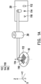
- FIG. 1A is a schematic diagram of a manufacturing method of an electronic device according to an embodiment of the disclosure.
- FIG. 1B is a schematic diagram of a first chip, a second chip, and a third chip on a second substrate in FIG. 1A .
- a first substrate 10 including a plurality of chips 110 is provided.
- the first substrate 10 may be a wafer, a glass substrate, or a polyimide substrate (PI), for example but not limited thereto.
- the first substrate 10 may be provided with a release film (e.g., a blue film) thereon.
- the release film is located between the first substrate 10 and the chips 110 to facilitate separation of the chips from the first substrate 10. Therefore, the first substrate 10 may be regarded as a temporary substrate.
- the first substrate 10 may have a chamfer, an arc, or any other shape.
- the chips 110 may be packaged or bare, and may also be a capacitor, a resistor, an inductor, a variable capacitor, a filter, a diode, a transistor, a sensor, MEMS, a liquid crystal chip, for example but not limited thereto.
- the diode may include a light-emitting diode or a non-light-emitting diode.
- the diode include a P-N junction diode, a PIN diode, or a constant current diode.
- the light-emitting diode may include an organic light-emitting diode (OLED), a mini LED, a micro LED, a quantum dot LED, fluorescence, phosphor, or other suitable materials or a combination thereof, for example but not limited thereto.
- the sensor may include a capacitive sensor, an optical sensor, an electromagnetic sensor, a fingerprint sensor (FPS), a touch sensor, an antenna, or a pen sensor, for example but not limited thereto.
- a second substrate 20 and a pick-and-place device 30 are provided.
- the first substrate 10 and the second substrate 20 may be respectively located on opposite sides of the pick-and-place device 30, but not limited thereto.
- the first substrate 10 and the second substrate 20 are disposed on the X-Y plane, and the pick-and-place device 30 may move on the X-Y plane.
- the second substrate 20 may be a wafer, a glass substrate, or a polyimide substrate, for example but not limited thereto.
- the second substrate 20 may have a chamfer, an arc, or any other shape.
- a transfer process is performed to sequentially transfer a first chip 112 and a second chip 114 among the chips 110 to the second substrate 20.
- the second chip 114 is adjacent to the first chip 112 on the second substrate 20. Therefore, the second substrate 20 may be regarded as a target substrate.
- the first chip 112 and the second chip 114 may be in the same shape or in different shapes.
- the shape of the first chip 112 is a rectangle with rounded corners
- the shape of the second chip 114 is a rhombus, for example but not limited thereto.
- the transfer process is rotating the first substrate 10, for example. In other words, the first substrate 10 is rotated relative to the X-axis, while the second substrate 20 remains stationary.
- the pick-and-place device 30 picks up the first chip 112 from the first substrate 10 and places the first chip 112 on the second substrate 20.
- the pick-and-place device 30 picks up the second chip 114 from the first substrate 10 and places the second chip 114 adjacent to the first chip 112 on the second substrate 20.
- a first angle A1 is between a first extension direction D1 of a first side S1 (i.e., a long side) of the first chip 112 and an extension direction D of a first boundary B of the second substrate 20.
- a second angle A2 is between a second extension direction D2 of a second side S2 of the second chip 114 and the extension direction D of the first boundary B of the second substrate 20.
- the first angle A1 is different from the second angle A2.
- the first angle A1 is greater than 0 and less than or equal to 90 degrees
- the second angle A2 is greater than 0 and less than or equal to 90 degrees.
- a difference between the first angle A1 and the second angle A2 is less than 90 degrees, for example.
- the difference between the first angle A1 and the second angle A2 is less than 45 degrees, for example. In another embodiment, the difference between the first angle A1 and the second angle A2 is less than 20 degrees, for example.
- the boundary B may be the long side of the substrate, and the sides may be the long sides of the chips. Alternatively, when side lengths of the chip are the same, the side adjacent to the long side of the substrate is taken as the reference, but not limited thereto.
- the above-mentioned steps may also be repeated to further transfer a third chip 116 among the chips 110 to the second substrate 20.
- the third chip 116 is adjacent to the second chip 114, and the second chip 114 is located between the first chip 112 and the third chip 116, but not limited thereto.
- the shape of the third chip 116 is a triangle, for example but not limited thereto.
- a third angle A3 is between a third extension direction D3 of a third side S3 of the third chip 116 and the extension direction D of the first boundary B of the second substrate 20.
- the third angle A3 is different from the first angle A1 and the second angle A2.
- the third angle A3 is greater than 0 and less than or equal to 90 degrees, for example.
- a difference between the first angle A1, the second angle A2, and the third angle A3 is less than 90 degrees, for example.
- the difference between the first angle A1, the second angle A2, and the third angle A3 is less than 45 degrees, for example.
- the difference between the first angle A1, the second angle A2, and the third angle A3 is less than 20 degrees, for example.
- the manufacturing method of an electronic device of the disclosure can meet the diverse requirements of users who need to change the angle of the chips on the target substrate for appearance reliability or electrical requirements.
- FIG. 2 is a schematic diagram of a manufacturing method of an electronic device according to another embodiment of the disclosure.
- the manufacturing method of an electronic device of this embodiment is similar to the manufacturing method of an electronic device of FIG. 1A .
- this embodiment also includes forming a metal layer 120 and an opening hole H after providing the second substrate 20 and before performing the transfer process.
- the metal layer 120 is located between the second substrate 20 and the first chip 112.
- An orthogonal projection of the first chip 112 on the second substrate 20 is overlapped with the opening hole H.
- the metal layer 120 may be formed on the second substrate 20 and covered by a dielectric layer 125 having the opening hole H.
- the first chip 112 may be disposed in the opening hole H of the dielectric layer 125 and electrically connected to the metal layer 120 through a solder T1.
- a pad 130 may be further between the second chip 114 and the metal layer 120.
- the first chip 112 may be electrically connected to the pad 130 through a solder T2, and the second chip 114 is directly disposed on the pad 130.
- the first chip 112 is a light-emitting diode
- the second chip 114 is an active element, such as a thin film transistor, for example but not limited thereto.
- the metal layer 120 includes copper (Cu), titanium (Ti), or aluminum (Al), for example but not limited thereto.
- a spacer 140 is formed on the dielectric layer 125.
- a protective layer 150 is formed on the first chip 112 and the second chip 114 to protect the first chip 112 and the second chip 114. Disposing the spacer 140 maintains the distance between the protective layer 150 and the first chip 112 and the second chip 114.
- a sealing member 160 is between a periphery of the second substrate 20 and a periphery of the protective layer 150 to prevent moisture and oxygen from eroding the first chip 112, the second chip 114, the metal layer 120, and the pad 130.
- the sealing member 160 is formed adjacent to the boundary of the second substrate 20. So far, an electronic device 100 is completed.
- the electronic device 100 may include a display device, an antenna device, a sensing device, a light-emitting device, a packaging device, or a tiled device, but not limited thereto.
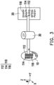
- FIG. 3 is a schematic diagram of a manufacturing method of an electronic device according to another embodiment of the disclosure.
- the manufacturing method of an electronic device of this embodiment is similar to the manufacturing method of an electronic device of FIG. 1A .
- the difference between them is that in this embodiment, the first substrate 10 and the second substrate 20 are disposed on the X-Z plane.
- the pick-and-place device 30 may move in the X-Z plane, and the transfer process is rotating the first substrate 10, for example. In other words, the first substrate 10 is rotated relative to the Z-axis, while the second substrate 20 remains stationary.
- FIG. 4 is a schematic diagram of a manufacturing method of an electronic device according to another embodiment of the disclosure.
- the manufacturing method of an electronic device of this embodiment is similar to the manufacturing method of an electronic device of FIG. 1A .
- the difference between them is that in this embodiment, the first substrate 10 and the second substrate 20 are disposed on the X-Y plane.
- the pick-and-place device 30 may move in the X-Y plane, and the transfer process is rotating the second substrate 20, for example. In other words, the second substrate 20 is rotated relative to the X-axis, while the first substrate 10 remains stationary.
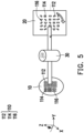
- FIG. 5 is a schematic diagram of a manufacturing method of an electronic device according to another embodiment of the disclosure.
- the manufacturing method of an electronic device of this embodiment is similar to the manufacturing method of an electronic device of FIG. 1A .
- the difference between them is that in this embodiment, the first substrate 10 and the second substrate 20 are disposed on the X-Z plane.
- the pick-and-place device 30 may move in the X-Z plane, and the transfer process is rotating the second substrate 20, for example. In other words, the second substrate 20 is rotated relative to the Z-axis, while the first substrate 10 remains stationary.
- FIG. 6 is a schematic diagram of a manufacturing method of an electronic device according to another embodiment of the disclosure.
- the manufacturing method of an electronic device of this embodiment is similar to the manufacturing method of an electronic device of FIG. 1A .
- the difference between them is that in this embodiment, the first substrate 10 and the second substrate 20 are disposed on the X-Y plane.
- the pick-and-place device 30 may be moved in the X-Y plane, and the transfer process includes rotating a rotary disk 40 disposed on the pick-and-place device 30, for example.
- the arrangement angles of the first chip 112, the second chip 114, and the third chip 116 after transferred to the second substrate 20 may be changed by rotating the rotary disk 40.
- the first substrate 10 and the second substrate 20 remain stationary during the transfer process.
- FIG. 7 is a schematic diagram of a manufacturing method of an electronic device according to another embodiment of the disclosure.
- the manufacturing method of an electronic device of this embodiment is similar to the manufacturing method of an electronic device of FIG. 6 .
- the difference between them is that a first substrate 10' of this embodiment and the first substrate 10 in FIG. 6 are in different structural forms.
- the first substrate 10' is embodied as a flexible substrate, such as a tape, but not limited thereto.
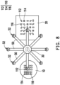
- FIG. 8 is a schematic diagram of a manufacturing method of an electronic device according to another embodiment of the disclosure.
- the manufacturing method of an electronic device of this embodiment is similar to the manufacturing method of an electronic device of FIG. 1A .
- the pick-and-place device 30 includes a plurality of robot arms 50 each having a rotary disk 52 at the front end.
- the transfer process includes rotating the rotary disk 52 of the robot arm 50.
- the arrangement angles of the first chip 112, the second chip 114, and the third chip 116 after transferred to the second substrate 20 may be changed by independently controlling the rotary disk 52 of each of the robot arms 50 to rotate the rotary disks 52 by different angles, which accelerates the pick-and-place process to reduce the manufacturing time.
Landscapes
- Wire Bonding (AREA)
- Solid State Image Pick-Up Elements (AREA)
- Light Receiving Elements (AREA)
- Semiconductor Integrated Circuits (AREA)
Abstract
Description
- The disclosure relates to an electronic device and a manufacturing method of an electronic device. In particular, the disclosure relates to an electronic device and a manufacturing method of an electronic device that can meet diverse requirements of users.
- Currently, since a transfer machine can only move in an X-Y plane, a temporary substrate with a release film (e.g., a blue film) and chips mounted thereon moves at a fixed angle. Thus, during transfer of the chips from the temporary substrate to a target substrate, the chips are only at a single angle on the target substrate. Accordingly, if users need to change the angle of the chips on the target substrate for appearance reliability or electrical requirements, major operation of first suspending the production line is required to change settings of the machine or the like, which is relatively costly.
- The disclosure is directed to an electronic device and a manufacturing method of an electronic device, in which extension directions of sides of a plurality of transferred chips can respectively form a plurality of different angles with an extension direction of a boundary of a substrate.
- According to an embodiment of the disclosure, a manufacturing method of an electronic device includes the following. A first substrate is provided. The first substrate includes a plurality of chips. A second substrate is provided. A transfer process is performed to sequentially transfer a first chip and a second chip among the plurality of chips to the second substrate. The second chip is adjacent to the first chip. A first angle is between a first extension direction of a first side of the first chip and an extension direction of a first boundary of the second substrate. A second angle is between a second extension direction of a second side of the second chip and the extension direction of the first boundary of the second substrate. The first angle is different from the second angle.
- According to an embodiment of the disclosure, an electronic device includes a substrate, a first chip, and a second chip. The first chip and the second chip are disposed on the substrate. The second chip is adjacent to the first chip. A first angle is between a first extension direction of a first side of the first chip and an extension direction of a first boundary of the second substrate. A second angle is between a second extension direction of a second side of the second chip and the extension direction of the first boundary of the second substrate. The first angle is different from the second angle.
- Based on the foregoing, in the embodiments of the disclosure, different angles are between the extension directions of the sides of the first chip and the second chip and the extension direction of the boundary of the second substrate after the first chip and the second chip are sequentially transferred to the second substrate. Compared with the existing technology, in which only a single angle is between the transferred chips and the substrate, the manufacturing method of an electronic device of the disclosure can meet the diverse requirements of users.
- To make the aforementioned more comprehensible, several embodiments accompanied with drawings are described in detail as follows.
- The accompanying drawings are included to provide a further understanding of the disclosure, and are incorporated in and constitute a part of this specification. The drawings illustrate exemplary embodiments of the disclosure and, together with the description, serve to explain the principles of the disclosure.
-
FIG. 1A is a schematic diagram of a manufacturing method of an electronic device according to an embodiment of the disclosure. -
FIG. 1B is a schematic diagram of a first chip, a second chip, and a third chip on a second substrate inFIG. 1A . -
FIG. 2 is a schematic diagram of a manufacturing method of an electronic device according to another embodiment of the disclosure. -
FIG. 3 is a schematic diagram of a manufacturing method of an electronic device according to another embodiment of the disclosure. -
FIG. 4 is a schematic diagram of a manufacturing method of an electronic device according to another embodiment of the disclosure. -
FIG. 5 is a schematic diagram of a manufacturing method of an electronic device according to another embodiment of the disclosure. -
FIG. 6 is a schematic diagram of a manufacturing method of an electronic device according to another embodiment of the disclosure. -
FIG. 7 is a schematic diagram of a manufacturing method of an electronic device according to another embodiment of the disclosure. -
FIG. 8 is a schematic diagram of a manufacturing method of an electronic device according to another embodiment of the disclosure. - Reference will now be made in detail to exemplary embodiments of the disclosure, examples of which are illustrated in the accompanying drawings. Wherever possible, the same reference numerals are used in the drawings and description to refer to the same or like parts.
- The disclosure may be understood with reference to the following detailed description together with the accompanying drawings. It should be noted that, for ease of understanding by readers and conciseness of the drawings, a plurality of drawings in the disclosure merely show a part of an electronic device, and specific elements in the drawings are not drawn to scale. In addition, the number and size of the elements in the drawings only serve for exemplifying instead of limiting the scope of the disclosure.
- Certain terms are used throughout the description and the appended claims to refer to specific elements. Those skilled in the art should understand that electronic device manufacturers may refer to the same element by different names. Herein, it is not intended to distinguish between elements that have the same function but have different names.
- In the following description and claims, terms such as "include", "comprise", and "have" are open-ended terms, and thus should be interpreted as "including, but not limited to".
- In addition, relative terms, such as "below" or "bottom" and "above" or "top," may be used in the embodiments to describe the relative relationship of one element to another element of the drawings. It will be understandable that if the device in the drawings is turned upside down, elements described on the "lower" side will become elements described on the "upper" side.
- In some embodiments of the disclosure, terms related to bonding and connection such as "connection", "interconnection", etc., unless specifically defined, may indicate the case where two structures are in direct contact, or where two structures are not in direct contact and other structures are disposed in between. Moreover, such terms related to bonding and connection may also cover the case where two structures are both movable or where two structures are both fixed. Furthermore, the term "coupling" includes transfer of energy between two structures by means of direct or indirect electrical connection, or transfer of energy between two separate structures by means of mutual induction.
- It should be understood that when an element or film layer is referred to as being "on", or "connected to" another element or film layer, the element or film layer may be directly on or connected to the another element or film layer, or intervening elements or film layers may also be present in between (non-direct circumstances). In contrast, when an element or film layer is referred to as being "directly on" or "directly connected to" another element or film layer, no intervening elements or film layers are present in between.
- The term "about", "equal to", "equivalent" or "same", "substantially", or "essentially" is typically interpreted so that a value is within 20% of a given value or range, or within 10%, 5%, 3%, 2%, 1%, or 0.5% of a given value or range.
- As used herein, the term(s) "film" and/or "layer" may refer to any continuous or discontinuous structure and material (e.g., materials deposited by the methods disclosed herein). For example, films and/or layers may include two-dimensional materials, three-dimensional materials, nanoparticles, or even partial or complete molecular layers, or partial or complete atomic layers, or atomic and/or molecular clusters. The films or layers may include materials or layers having pinholes and may be at least partially continuous.
- Although the terms first, second, third, and so on may be used to describe diverse constituent elements, such constituent elements are not limited by the terms. The terms are used only to discriminate one constituent element from other constituent elements in the description. In the claims, the terms first, second, third, etc. may be used in accordance with the order of claiming elements instead of using the same terms. Accordingly, a first constituent element in the following description may be a second constituent element in the claims.
- Unless otherwise defined, all terms (including technical and scientific terms) used herein have the same meaning as commonly understood by one of ordinary skill in the art. It is understandable that these terms, such as those defined in commonly used dictionaries, should be interpreted to have a meaning consistent with the background or context of the related art and the disclosure, and not interpreted in an idealized or overly formal manner, unless specifically defined herein.
- It should be noted that features in several different embodiments below may be replaced, recombined, mixed with each other to achieve other embodiments without departing from the spirit of the disclosure.
- The electronic device of the disclosure may include, but is not limited to, a display device, an antenna device, a sensing device, a light-emitting device, or a tiled device. The electronic device may include a bendable or flexible electronic device. The electronic device may include electronic components. The electronic components may include passive elements, active elements, or a combination thereof, for example, a capacitor, a resistor, an inductor, a variable capacitor, a filter, a diode, a transistor, a sensor, MEMS, a liquid crystal chip, but not limited thereto. The diode may include a light-emitting diode (LED) or a non-light-emitting diode. The diode include a P-N junction diode, a PIN diode, or a constant current diode. The light-emitting diode may include an organic light-emitting diode (OLED), a mini LED, a micro LED, a quantum dot LED, fluorescence, phosphor, or other suitable materials or a combination thereof, for example but not limited thereto. The sensor may include a capacitive sensor, an optical sensor, an electromagnetic sensor, a fingerprint sensor (FPS), a touch sensor, an antenna, or a pen sensor, for example but not limited thereto. Hereinafter, a display device will be taken as the electronic device to describe the disclosure, but the disclosure is not limited thereto.
- Reference will now be made in detail to exemplary embodiments of the disclosure, examples of which are illustrated in the accompanying drawings. Wherever possible, the same reference numerals are used in the drawings and description to refer to the same or like parts.
-
FIG. 1A is a schematic diagram of a manufacturing method of an electronic device according to an embodiment of the disclosure.FIG. 1B is a schematic diagram of a first chip, a second chip, and a third chip on a second substrate inFIG. 1A . - First, reference may be made to
FIG. 1A for the manufacturing method of an electronic device of this embodiment. First, afirst substrate 10 including a plurality ofchips 110 is provided. Thefirst substrate 10 may be a wafer, a glass substrate, or a polyimide substrate (PI), for example but not limited thereto. In an embodiment, thefirst substrate 10 may be provided with a release film (e.g., a blue film) thereon. The release film is located between thefirst substrate 10 and thechips 110 to facilitate separation of the chips from thefirst substrate 10. Therefore, thefirst substrate 10 may be regarded as a temporary substrate. In an embodiment, thefirst substrate 10 may have a chamfer, an arc, or any other shape. Thechips 110 may be packaged or bare, and may also be a capacitor, a resistor, an inductor, a variable capacitor, a filter, a diode, a transistor, a sensor, MEMS, a liquid crystal chip, for example but not limited thereto. The diode may include a light-emitting diode or a non-light-emitting diode. The diode include a P-N junction diode, a PIN diode, or a constant current diode. The light-emitting diode may include an organic light-emitting diode (OLED), a mini LED, a micro LED, a quantum dot LED, fluorescence, phosphor, or other suitable materials or a combination thereof, for example but not limited thereto. The sensor may include a capacitive sensor, an optical sensor, an electromagnetic sensor, a fingerprint sensor (FPS), a touch sensor, an antenna, or a pen sensor, for example but not limited thereto. - Next, with continued reference to
FIG. 1A , asecond substrate 20 and a pick-and-place device 30 are provided. Thefirst substrate 10 and thesecond substrate 20 may be respectively located on opposite sides of the pick-and-place device 30, but not limited thereto. Here, for example, thefirst substrate 10 and thesecond substrate 20 are disposed on the X-Y plane, and the pick-and-place device 30 may move on the X-Y plane. Thesecond substrate 20 may be a wafer, a glass substrate, or a polyimide substrate, for example but not limited thereto. In an embodiment, thesecond substrate 20 may have a chamfer, an arc, or any other shape. - After that, a transfer process is performed to sequentially transfer a
first chip 112 and asecond chip 114 among thechips 110 to thesecond substrate 20. Thesecond chip 114 is adjacent to thefirst chip 112 on thesecond substrate 20. Therefore, thesecond substrate 20 may be regarded as a target substrate. Thefirst chip 112 and thesecond chip 114 may be in the same shape or in different shapes. Here, the shape of thefirst chip 112 is a rectangle with rounded corners, and the shape of thesecond chip 114 is a rhombus, for example but not limited thereto. Here, the transfer process is rotating thefirst substrate 10, for example. In other words, thefirst substrate 10 is rotated relative to the X-axis, while thesecond substrate 20 remains stationary. - Further, with reference to
FIG. 1A andFIG. 1B together, after thefirst substrate 10 including thechips 110 is rotated by an angle relative to the X-axis, the pick-and-place device 30 picks up thefirst chip 112 from thefirst substrate 10 and places thefirst chip 112 on thesecond substrate 20. Next, after thefirst substrate 10 is rotated by another angle relative to the X-axis, the pick-and-place device 30 picks up thesecond chip 114 from thefirst substrate 10 and places thesecond chip 114 adjacent to thefirst chip 112 on thesecond substrate 20. At this time, a first angle A1 is between a first extension direction D1 of a first side S1 (i.e., a long side) of thefirst chip 112 and an extension direction D of a first boundary B of thesecond substrate 20. In addition, a second angle A2 is between a second extension direction D2 of a second side S2 of thesecond chip 114 and the extension direction D of the first boundary B of thesecond substrate 20. In particular, the first angle A1 is different from the second angle A2. Here, for example, the first angle A1 is greater than 0 and less than or equal to 90 degrees, and the second angle A2 is greater than 0 and less than or equal to 90 degrees. A difference between the first angle A1 and the second angle A2 is less than 90 degrees, for example. In an embodiment, the difference between the first angle A1 and the second angle A2 is less than 45 degrees, for example. In another embodiment, the difference between the first angle A1 and the second angle A2 is less than 20 degrees, for example. Here, for example, the boundary B may be the long side of the substrate, and the sides may be the long sides of the chips. Alternatively, when side lengths of the chip are the same, the side adjacent to the long side of the substrate is taken as the reference, but not limited thereto. - Next, with reference to
FIG. 1A andFIG. 1B together, the above-mentioned steps may also be repeated to further transfer athird chip 116 among thechips 110 to thesecond substrate 20. Thethird chip 116 is adjacent to thesecond chip 114, and thesecond chip 114 is located between thefirst chip 112 and thethird chip 116, but not limited thereto. The shape of thethird chip 116 is a triangle, for example but not limited thereto. A third angle A3 is between a third extension direction D3 of a third side S3 of thethird chip 116 and the extension direction D of the first boundary B of thesecond substrate 20. In addition, the third angle A3 is different from the first angle A1 and the second angle A2. Here, the third angle A3 is greater than 0 and less than or equal to 90 degrees, for example. A difference between the first angle A1, the second angle A2, and the third angle A3 is less than 90 degrees, for example. In an embodiment, the difference between the first angle A1, the second angle A2, and the third angle A3 is less than 45 degrees, for example. In another embodiment, the difference between the first angle A1, the second angle A2, and the third angle A3 is less than 20 degrees, for example. - In brief, in this embodiment, the
first chip 112, after thesecond chip 114, and thethird chip 116 are sequentially transferred to thesecond substrate 20, the first angle A1, the second angle A2, and the third angle A3 of different angles are respectively between the extension direction D of the first boundary B of thesecond substrate 20 and the first extension direction D1 of the first side S1, the second extension direction D2 of the second side S2, and the third extension direction D3 of the third side S3. Compared with the existing technology, in which only a single angle is between the transferred chips and the substrate, the manufacturing method of an electronic device of the disclosure can meet the diverse requirements of users who need to change the angle of the chips on the target substrate for appearance reliability or electrical requirements. - It should be noted here that reference numerals and partial contents of the embodiments above remain to be used in the following embodiments, and the same reference numerals are used to refer to the same or like elements, and the description of the same technical content is omitted. Reference may be made to the embodiments above for the description of the omitted part, which will not be repeated in the following embodiments.
-
FIG. 2 is a schematic diagram of a manufacturing method of an electronic device according to another embodiment of the disclosure. With reference toFIG. 1A andFIG. 2 together, the manufacturing method of an electronic device of this embodiment is similar to the manufacturing method of an electronic device ofFIG. 1A . The difference between them is that this embodiment also includes forming ametal layer 120 and an opening hole H after providing thesecond substrate 20 and before performing the transfer process. Themetal layer 120 is located between thesecond substrate 20 and thefirst chip 112. An orthogonal projection of thefirst chip 112 on thesecond substrate 20 is overlapped with the opening hole H. Further, themetal layer 120 may be formed on thesecond substrate 20 and covered by adielectric layer 125 having the opening hole H. Thefirst chip 112 may be disposed in the opening hole H of thedielectric layer 125 and electrically connected to themetal layer 120 through a solder T1. Next, a pad 130 may be further between thesecond chip 114 and themetal layer 120. Thefirst chip 112 may be electrically connected to the pad 130 through a solder T2, and thesecond chip 114 is directly disposed on the pad 130. Here, thefirst chip 112 is a light-emitting diode, and thesecond chip 114 is an active element, such as a thin film transistor, for example but not limited thereto. In addition, themetal layer 120 includes copper (Cu), titanium (Ti), or aluminum (Al), for example but not limited thereto. - Furthermore, a
spacer 140 is formed on thedielectric layer 125. Next, aprotective layer 150 is formed on thefirst chip 112 and thesecond chip 114 to protect thefirst chip 112 and thesecond chip 114. Disposing thespacer 140 maintains the distance between theprotective layer 150 and thefirst chip 112 and thesecond chip 114. Finally, a sealingmember 160 is between a periphery of thesecond substrate 20 and a periphery of theprotective layer 150 to prevent moisture and oxygen from eroding thefirst chip 112, thesecond chip 114, themetal layer 120, and the pad 130. For example, the sealingmember 160 is formed adjacent to the boundary of thesecond substrate 20. So far, anelectronic device 100 is completed. Here, theelectronic device 100 may include a display device, an antenna device, a sensing device, a light-emitting device, a packaging device, or a tiled device, but not limited thereto. According to another embodiment, it is also possible to first form the sealingmember 160 on the periphery of thesecond substrate 20, and then form theprotective layer 150 on thesecond substrate 20 and thespacer 140, but not limited thereto. -
FIG. 3 is a schematic diagram of a manufacturing method of an electronic device according to another embodiment of the disclosure. With reference toFIG. 1A andFIG. 3 together, the manufacturing method of an electronic device of this embodiment is similar to the manufacturing method of an electronic device ofFIG. 1A . The difference between them is that in this embodiment, thefirst substrate 10 and thesecond substrate 20 are disposed on the X-Z plane. In addition, the pick-and-place device 30 may move in the X-Z plane, and the transfer process is rotating thefirst substrate 10, for example. In other words, thefirst substrate 10 is rotated relative to the Z-axis, while thesecond substrate 20 remains stationary. -
FIG. 4 is a schematic diagram of a manufacturing method of an electronic device according to another embodiment of the disclosure. With reference toFIG. 1A andFIG. 4 together, the manufacturing method of an electronic device of this embodiment is similar to the manufacturing method of an electronic device ofFIG. 1A . The difference between them is that in this embodiment, thefirst substrate 10 and thesecond substrate 20 are disposed on the X-Y plane. In addition, the pick-and-place device 30 may move in the X-Y plane, and the transfer process is rotating thesecond substrate 20, for example. In other words, thesecond substrate 20 is rotated relative to the X-axis, while thefirst substrate 10 remains stationary. -
FIG. 5 is a schematic diagram of a manufacturing method of an electronic device according to another embodiment of the disclosure. With reference toFIG. 1A andFIG. 5 together, the manufacturing method of an electronic device of this embodiment is similar to the manufacturing method of an electronic device ofFIG. 1A . The difference between them is that in this embodiment, thefirst substrate 10 and thesecond substrate 20 are disposed on the X-Z plane. In addition, the pick-and-place device 30 may move in the X-Z plane, and the transfer process is rotating thesecond substrate 20, for example. In other words, thesecond substrate 20 is rotated relative to the Z-axis, while thefirst substrate 10 remains stationary. -
FIG. 6 is a schematic diagram of a manufacturing method of an electronic device according to another embodiment of the disclosure. With reference toFIG. 1A andFIG. 6 together, the manufacturing method of an electronic device of this embodiment is similar to the manufacturing method of an electronic device ofFIG. 1A . The difference between them is that in this embodiment, thefirst substrate 10 and thesecond substrate 20 are disposed on the X-Y plane. In addition, the pick-and-place device 30 may be moved in the X-Y plane, and the transfer process includes rotating arotary disk 40 disposed on the pick-and-place device 30, for example. In other words, the arrangement angles of thefirst chip 112, thesecond chip 114, and thethird chip 116 after transferred to thesecond substrate 20 may be changed by rotating therotary disk 40. In other words, thefirst substrate 10 and thesecond substrate 20 remain stationary during the transfer process. -
FIG. 7 is a schematic diagram of a manufacturing method of an electronic device according to another embodiment of the disclosure. With reference toFIG. 6 andFIG. 7 together, the manufacturing method of an electronic device of this embodiment is similar to the manufacturing method of an electronic device ofFIG. 6 . The difference between them is that a first substrate 10' of this embodiment and thefirst substrate 10 inFIG. 6 are in different structural forms. The first substrate 10' is embodied as a flexible substrate, such as a tape, but not limited thereto. -
FIG. 8 is a schematic diagram of a manufacturing method of an electronic device according to another embodiment of the disclosure. With reference toFIG. 1A andFIG. 8 together, the manufacturing method of an electronic device of this embodiment is similar to the manufacturing method of an electronic device ofFIG. 1A . The difference between them is that in this embodiment, the pick-and-place device 30 includes a plurality ofrobot arms 50 each having arotary disk 52 at the front end. In addition, the transfer process includes rotating therotary disk 52 of therobot arm 50. In an embodiment, for example, the arrangement angles of thefirst chip 112, thesecond chip 114, and thethird chip 116 after transferred to thesecond substrate 20 may be changed by independently controlling therotary disk 52 of each of therobot arms 50 to rotate therotary disks 52 by different angles, which accelerates the pick-and-place process to reduce the manufacturing time. - In summary of the foregoing, in the embodiments of the disclosure, different angles are between the extension directions of the sides of the first chip and the second chip and the extension direction of the boundary of the second substrate after the first chip and the second chip are sequentially transferred to the second substrate. Compared with the existing technology, in which only a single angle is between the transferred chips and the substrate, the manufacturing method of an electronic device of the disclosure can meet the diverse requirements of users.
Claims (15)
- A manufacturing method of an electronic device (100), comprising:providing a first substrate (10, 10') comprising a plurality of chips (110);providing a second substrate (20); andperforming a transfer process to sequentially transfer a first chip (112) and a second chip (114) among the plurality of chips (110) to the second substrate (20), wherein the second chip (114) is adjacent to the first chip (112), a first angle (A1) is between a first extension direction (D1) of a first side (S1) of the first chip (112) and an extension direction (D) of a first boundary (B) of the second substrate (20), a second angle (A2) is between a second extension direction (D2) of a second side (S2) of the second chip (114) and the extension direction (D) of the first boundary (B) of the second substrate (20), and the first angle (A1) is different from the second angle (A2).
- The manufacturing method according to claim 1, further comprising:
transferring a third chip (116) among the plurality of chips (110) to the second substrate (20), wherein the third chip (116) is adjacent to the second chip (114), a third angle (A3) is between a third extension direction (D3) of a third side (S3) of the third chip (116) and the extension direction (D) of the first boundary (B) of the second substrate (20), and the third angle (A3) is different from the first angle (A1) and the second angle (A2). - The manufacturing method according to claim 1, wherein a difference between the first angle (A1) and the second angle (A2) is less than 90 degrees.
- The manufacturing method according to claim 1, wherein the transfer process comprises rotating the first substrate (10,10').
- The manufacturing method according to claim 1, wherein the transfer process comprises rotating the second substrate (20).
- The manufacturing method according to claim 1, wherein the transfer process comprises rotating a rotary disk (52) of a robot arm (50).
- The manufacturing method according to claim 1, wherein the transfer process comprises rotating a rotary disk (40).
- The manufacturing method according to claim 1, further comprising:
forming a metal layer (120) and an opening hole (H), wherein the metal layer (120) is located between the second substrate (20) and one of the first chip (112) and the second chip (114), and an orthogonal projection of the one of the first chip (112) and the second chip (114) on the second substrate (20) is overlapped with the opening hole (H). - The manufacturing method according to claim 8, further comprising:
forming a pad (130) between the metal layer (120) and the other one of the first chip (112) and the second chip (114). - The manufacturing method according to claim 9, further comprising:
electrically connecting the one of the first chip (112) and the second chip (114) to the pad (130) through a solder (T1,T2), and directly disposing the other one of the first chip (112) and the second chip (114) on the pad (130). - The manufacturing method according to claim 1, further comprising:
forming a protective layer (150) on the first chip (112) and the second chip (114). - The manufacturing method according to claim 11, further comprising:
forming a sealing member (160) between a periphery of the second substrate (20) and a periphery of the protective layer (150). - The manufacturing method according to claim 1, wherein a difference between the first angle (A1) and the second angle (A2) is less than 45 degrees.
- The manufacturing method according to claim 1, wherein a difference between the first angle (A1) and the second angle (A2) is less than 20 degrees.
- An electronic device (100), comprising:a substrate (20); anda first chip (112) and a second chip (114) disposed on the substrate (20),wherein the second chip (114) is adjacent to the first chip (112), a first angle (A1) is between a first extension direction (D1) of a first side (S1) of the first chip (112) and an extension direction (D) of a first boundary (B) of the substrate (20), a second angle (A2) is between a second extension direction (D2) of a second side (S2) of the second chip (114) and the extension direction (D) of the first boundary (B) of the substrate (20), and the first angle (A1) is different from the second angle (A2).
Applications Claiming Priority (2)
| Application Number | Priority Date | Filing Date | Title |
|---|---|---|---|
| US202163233334P | 2021-08-16 | 2021-08-16 | |
| CN202210513602.1A CN115910891A (en) | 2021-08-16 | 2022-05-12 | Method for making an electronic device |
Publications (1)
| Publication Number | Publication Date |
|---|---|
| EP4141916A1 true EP4141916A1 (en) | 2023-03-01 |
Family
ID=83232762
Family Applications (1)
| Application Number | Title | Priority Date | Filing Date |
|---|---|---|---|
| EP22187736.8A Pending EP4141916A1 (en) | 2021-08-16 | 2022-07-29 | Electronic device and manufacturing method of electronic device |
Country Status (3)
| Country | Link |
|---|---|
| US (2) | US12341142B2 (en) |
| EP (1) | EP4141916A1 (en) |
| TW (1) | TWI833247B (en) |
Citations (2)
| Publication number | Priority date | Publication date | Assignee | Title |
|---|---|---|---|---|
| US20100186226A1 (en) * | 2006-06-23 | 2010-07-29 | University Of Washington, The | Fluidic self-assembly for system integration |
| US20190006564A1 (en) * | 2014-10-31 | 2019-01-03 | eLux Inc. | Encapsulated Fluid Assembly Emissive Elements |
Family Cites Families (8)
| Publication number | Priority date | Publication date | Assignee | Title |
|---|---|---|---|---|
| US8327253B2 (en) * | 2010-11-09 | 2012-12-04 | Shutterfly, Inc. | System and method for creating photo books using video |
| TW201320254A (en) * | 2011-11-15 | 2013-05-16 | 華新麗華股份有限公司 | Solid crystal device and solid crystal method |
| JP6337400B2 (en) | 2012-04-24 | 2018-06-06 | 須賀 唯知 | Chip-on-wafer bonding method, bonding apparatus, and structure including chip and wafer |
| DE102016113328B4 (en) * | 2015-08-31 | 2018-07-19 | Besi Switzerland Ag | Method for mounting bumped semiconductor chips on substrate sites of a substrate |
| JP7164314B2 (en) * | 2017-04-28 | 2022-11-01 | ベシ スウィッツァーランド エージー | APPARATUS AND METHOD FOR MOUNTING COMPONENTS ON SUBSTRATE |
| CN109950182A (en) * | 2019-03-29 | 2019-06-28 | 合肥鑫晟光电科技有限公司 | The flood tide transfer method and flood tide transfer device of Micro LED |
| US11972968B2 (en) * | 2020-07-02 | 2024-04-30 | Sharpack Technology Pte. Ltd. | Fluxless gang die bonding arrangement |
| KR102885871B1 (en) * | 2020-08-13 | 2025-11-12 | 삼성전자주식회사 | align method of micro emitting device and display transferring structure |
-
2022
- 2022-06-17 TW TW111122618A patent/TWI833247B/en active
- 2022-07-28 US US17/876,508 patent/US12341142B2/en active Active
- 2022-07-29 EP EP22187736.8A patent/EP4141916A1/en active Pending
-
2025
- 2025-05-27 US US19/218,654 patent/US20250286035A1/en active Pending
Patent Citations (2)
| Publication number | Priority date | Publication date | Assignee | Title |
|---|---|---|---|---|
| US20100186226A1 (en) * | 2006-06-23 | 2010-07-29 | University Of Washington, The | Fluidic self-assembly for system integration |
| US20190006564A1 (en) * | 2014-10-31 | 2019-01-03 | eLux Inc. | Encapsulated Fluid Assembly Emissive Elements |
Also Published As
| Publication number | Publication date |
|---|---|
| TW202310140A (en) | 2023-03-01 |
| US20230052081A1 (en) | 2023-02-16 |
| TWI833247B (en) | 2024-02-21 |
| US20250286035A1 (en) | 2025-09-11 |
| US12341142B2 (en) | 2025-06-24 |
Similar Documents
| Publication | Publication Date | Title |
|---|---|---|
| KR102763482B1 (en) | Display device | |
| CN105808005B (en) | Flexible display screen and manufacturing method thereof | |
| EP4235282A2 (en) | Display panel and display device | |
| CN106229332B (en) | Display panel, manufacturing method thereof and flexible display device | |
| TWI735241B (en) | Flexible display panel | |
| CN110429089A (en) | Driving backplane, manufacturing method thereof, and display device | |
| TW200812448A (en) | Flexible electronic assembly | |
| WO2018120693A1 (en) | Flexible touch screen and manufacturing method, display screen and manufacturing method, and display device | |
| CN111596796B (en) | A three-dimensional touch module, its driving method, and display device | |
| CN112835473B (en) | Display panel, display device and preparation method of display panel | |
| US12216871B2 (en) | Touch panel and manufacturing method therefor, and display touch device | |
| TW202008043A (en) | Array substrate and manufacturing method thereof, display device using the same and manufacturing method thereof | |
| CN106033753A (en) | Packaging module and substrate structure thereof | |
| CN105224117A (en) | Touch screen and manufacturing method thereof | |
| CN110246877A (en) | Flexible touching display screen and its display device | |
| CN105304824A (en) | Organic electroluminescent module and method of manufacturing the same | |
| US12341142B2 (en) | Electronic device and manufacturing method of electronic device | |
| CN113327919B (en) | Light-emitting substrate, preparation method thereof, display device and detection method | |
| WO2016107094A1 (en) | Circuit board and method for manufacture thereof, and display device | |
| TW201530728A (en) | Integrated circuit package system with embedded components and method of manufacturing the same | |
| CN115910891A (en) | Method for making an electronic device | |
| TWI872483B (en) | Display panel, tiled display device including the same and manufacturing method thereof | |
| US20230134317A1 (en) | Electrical connection structure and electronic device including the same | |
| CN111987085A (en) | Sensor, preparation method of sensor and electronic equipment | |
| CN1731573A (en) | wafer carrier |
Legal Events
| Date | Code | Title | Description |
|---|---|---|---|
| PUAI | Public reference made under article 153(3) epc to a published international application that has entered the european phase |
Free format text: ORIGINAL CODE: 0009012 |
|
| STAA | Information on the status of an ep patent application or granted ep patent |
Free format text: STATUS: THE APPLICATION HAS BEEN PUBLISHED |
|
| AK | Designated contracting states |
Kind code of ref document: A1 Designated state(s): AL AT BE BG CH CY CZ DE DK EE ES FI FR GB GR HR HU IE IS IT LI LT LU LV MC MK MT NL NO PL PT RO RS SE SI SK SM TR |
|
| STAA | Information on the status of an ep patent application or granted ep patent |
Free format text: STATUS: REQUEST FOR EXAMINATION WAS MADE |
|
| 17P | Request for examination filed |
Effective date: 20230829 |
|
| RBV | Designated contracting states (corrected) |
Designated state(s): AL AT BE BG CH CY CZ DE DK EE ES FI FR GB GR HR HU IE IS IT LI LT LU LV MC MK MT NL NO PL PT RO RS SE SI SK SM TR |