EP4138533A1 - Electronic device including shield can - Google Patents
Electronic device including shield can Download PDFInfo
- Publication number
- EP4138533A1 EP4138533A1 EP21787685.3A EP21787685A EP4138533A1 EP 4138533 A1 EP4138533 A1 EP 4138533A1 EP 21787685 A EP21787685 A EP 21787685A EP 4138533 A1 EP4138533 A1 EP 4138533A1
- Authority
- EP
- European Patent Office
- Prior art keywords
- printed circuit
- circuit board
- region
- electronic device
- interposer
- Prior art date
- Legal status (The legal status is an assumption and is not a legal conclusion. Google has not performed a legal analysis and makes no representation as to the accuracy of the status listed.)
- Granted
Links
Images


Classifications
-
- H—ELECTRICITY
- H05—ELECTRIC TECHNIQUES NOT OTHERWISE PROVIDED FOR
- H05K—PRINTED CIRCUITS; CASINGS OR CONSTRUCTIONAL DETAILS OF ELECTRIC APPARATUS; MANUFACTURE OF ASSEMBLAGES OF ELECTRICAL COMPONENTS
- H05K1/00—Printed circuits
- H05K1/02—Details
- H05K1/14—Structural association of two or more printed circuits
- H05K1/144—Stacked arrangements of planar printed circuit boards
-
- H—ELECTRICITY
- H04—ELECTRIC COMMUNICATION TECHNIQUE
- H04B—TRANSMISSION
- H04B1/00—Details of transmission systems, not covered by a single one of groups H04B3/00 - H04B13/00; Details of transmission systems not characterised by the medium used for transmission
- H04B1/38—Transceivers, i.e. devices in which transmitter and receiver form a structural unit and in which at least one part is used for functions of transmitting and receiving
-
- H—ELECTRICITY
- H04—ELECTRIC COMMUNICATION TECHNIQUE
- H04M—TELEPHONIC COMMUNICATION
- H04M1/00—Substation equipment, e.g. for use by subscribers
- H04M1/02—Constructional features of telephone sets
- H04M1/0202—Portable telephone sets, e.g. cordless phones, mobile phones or bar type handsets
- H04M1/026—Details of the structure or mounting of specific components
- H04M1/0277—Details of the structure or mounting of specific components for a printed circuit board assembly
-
- H—ELECTRICITY
- H05—ELECTRIC TECHNIQUES NOT OTHERWISE PROVIDED FOR
- H05K—PRINTED CIRCUITS; CASINGS OR CONSTRUCTIONAL DETAILS OF ELECTRIC APPARATUS; MANUFACTURE OF ASSEMBLAGES OF ELECTRICAL COMPONENTS
- H05K1/00—Printed circuits
- H05K1/02—Details
- H05K1/11—Printed elements for providing electric connections to or between printed circuits
- H05K1/115—Via connections; Lands around holes or via connections
-
- H—ELECTRICITY
- H05—ELECTRIC TECHNIQUES NOT OTHERWISE PROVIDED FOR
- H05K—PRINTED CIRCUITS; CASINGS OR CONSTRUCTIONAL DETAILS OF ELECTRIC APPARATUS; MANUFACTURE OF ASSEMBLAGES OF ELECTRICAL COMPONENTS
- H05K3/00—Apparatus or processes for manufacturing printed circuits
- H05K3/36—Assembling printed circuits with other printed circuits
- H05K3/361—Assembling flexible printed circuits with other printed circuits
- H05K3/363—Assembling flexible printed circuits with other printed circuits by soldering
-
- H—ELECTRICITY
- H05—ELECTRIC TECHNIQUES NOT OTHERWISE PROVIDED FOR
- H05K—PRINTED CIRCUITS; CASINGS OR CONSTRUCTIONAL DETAILS OF ELECTRIC APPARATUS; MANUFACTURE OF ASSEMBLAGES OF ELECTRICAL COMPONENTS
- H05K9/00—Screening of apparatus or components against electric or magnetic fields
- H05K9/0007—Casings
- H05K9/002—Casings with localised screening
- H05K9/0022—Casings with localised screening of components mounted on printed circuit boards [PCB]
- H05K9/0024—Shield cases mounted on a PCB, e.g. cans or caps or conformal shields
- H05K9/0026—Shield cases mounted on a PCB, e.g. cans or caps or conformal shields integrally formed from metal sheet
- H05K9/0028—Shield cases mounted on a PCB, e.g. cans or caps or conformal shields integrally formed from metal sheet with retainers or specific soldering features
-
- H—ELECTRICITY
- H05—ELECTRIC TECHNIQUES NOT OTHERWISE PROVIDED FOR
- H05K—PRINTED CIRCUITS; CASINGS OR CONSTRUCTIONAL DETAILS OF ELECTRIC APPARATUS; MANUFACTURE OF ASSEMBLAGES OF ELECTRICAL COMPONENTS
- H05K1/00—Printed circuits
- H05K1/02—Details
- H05K1/14—Structural association of two or more printed circuits
- H05K1/141—One or more single auxiliary printed circuits mounted on a main printed circuit, e.g. modules, adapters
-
- H—ELECTRICITY
- H05—ELECTRIC TECHNIQUES NOT OTHERWISE PROVIDED FOR
- H05K—PRINTED CIRCUITS; CASINGS OR CONSTRUCTIONAL DETAILS OF ELECTRIC APPARATUS; MANUFACTURE OF ASSEMBLAGES OF ELECTRICAL COMPONENTS
- H05K2201/00—Indexing scheme relating to printed circuits covered by H05K1/00
- H05K2201/04—Assemblies of printed circuits
- H05K2201/042—Stacked spaced PCBs; Planar parts of folded flexible circuits having mounted components in between or spaced from each other
-
- H—ELECTRICITY
- H05—ELECTRIC TECHNIQUES NOT OTHERWISE PROVIDED FOR
- H05K—PRINTED CIRCUITS; CASINGS OR CONSTRUCTIONAL DETAILS OF ELECTRIC APPARATUS; MANUFACTURE OF ASSEMBLAGES OF ELECTRICAL COMPONENTS
- H05K2201/00—Indexing scheme relating to printed circuits covered by H05K1/00
- H05K2201/10—Details of components or other objects attached to or integrated in a printed circuit board
- H05K2201/10227—Other objects, e.g. metallic pieces
- H05K2201/10371—Shields or metal cases
-
- H—ELECTRICITY
- H05—ELECTRIC TECHNIQUES NOT OTHERWISE PROVIDED FOR
- H05K—PRINTED CIRCUITS; CASINGS OR CONSTRUCTIONAL DETAILS OF ELECTRIC APPARATUS; MANUFACTURE OF ASSEMBLAGES OF ELECTRICAL COMPONENTS
- H05K2201/00—Indexing scheme relating to printed circuits covered by H05K1/00
- H05K2201/10—Details of components or other objects attached to or integrated in a printed circuit board
- H05K2201/10227—Other objects, e.g. metallic pieces
- H05K2201/10378—Interposers
Definitions
- Various embodiments of the disclosure relate to an electronic device including a shield can.
- a structure in which a plurality of printed circuit boards are stacked by using an interposer has been proposed.
- a mounting space for electronic components may be secured in an electronic device by disposing a second printed circuit board on a first printed circuit board, and electrically connecting the first printed circuit board and the second printed circuit board by using an interposer.
- a structure in which a plurality of printed circuit boards are stacked by using an interposer may make it possible to secure a mounting space for electronic components, but may be vulnerable to damage or fracture due to an external force.
- a method of increasing physical connection strength of the plurality of printed circuit boards and/or the interposer is required.
- soldering the plurality of printed circuit boards and the interposer As a method of increasing physical connection strength of the plurality of printed circuit boards and/or the interposer, there has been proposed a method of soldering the plurality of printed circuit boards and the interposer to each other.
- the solder regions are relatively weak in rigidity compared to other components (e.g., a plurality of printed circuit boards or an interposer)
- the solder regions may be fractured (or "cracked") prior to the plurality of printed circuit boards and /or the interposer.
- connection strength between the plurality of printed circuit boards and the interposer may not be secured, or defects may be caused in the plurality of printed circuit boards and/or the interposer. Therefore, there is a need for a new method for increasing the connection strength between the plurality of printed circuit boards and the interposer without causing defects in the printed circuit boards and the interposer.
- various embodiments of the disclosure provide an electronic device in which physical connection strength between a plurality of printed circuit boards and an interposer is capable of being reinforced by expanding a partial region of a shield can provided on the printed circuit boards.
- An electronic device may include: a first printed circuit board including a first surface facing a first direction and a second surface facing a second direction opposite to the first direction; a second printed circuit board disposed to be spaced apart from the first printed circuit board and including a third surface facing the first direction and a fourth surface facing the first surface of the first printed circuit board; at least one electronic component disposed on the first printed circuit board and the second printed circuit board; an interposer located between the first printed circuit board and the second printed circuit board and electrically connecting the first printed circuit board and the second printed circuit board; and a shield structure located on at least one region of the third surface of the second printed circuit board and electromagnetically shielding the at least one electronic component, wherein the shield structure may include: a body located on the third surface of the second printed circuit board; and a first extension protruding from the body and connecting the body and the first printed circuit board, and wherein the first extension may include: a first portion protruding in a third direction perpendicular to the first direction with reference to
- An electronic device may include: a first printed circuit board including a first surface facing a first direction and a second surface facing a second direction opposite to the first direction; a second printed circuit board disposed to be spaced apart from the first printed circuit board and including a third surface facing the first direction and a fourth surface facing the first surface of the first printed circuit board; at least one electronic component disposed on the first printed circuit board and the second printed circuit board; an interposer located between the first printed circuit board and the second printed circuit board and electrically connecting the first printed circuit board and the second printed circuit board; and a shield structure located on at least one region of the third surface of the second printed circuit board and electromagnetically shielding the at least one electronic component, wherein the shield structure may include: a body located on the third surface of the second printed circuit board; and a first extension protruding from the body and connecting the body and the first printed circuit board, and wherein the first extension may include: a first portion extending along a third direction perpendicular to the first direction with reference to the body
- a printed circuit board stack structure including a first printed circuit board, an interposer, and/or a second printed circuit board.
- a shield structure e.g., a shield can
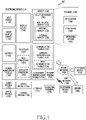
- Fig. 1 is a block diagram illustrating an electronic device 101 in a network environment 100 according to various embodiments.
- the electronic device 101 in the network environment 100 may communicate with an electronic device 102 via a first network 198 (e.g., a short-range wireless communication network), or an electronic device 104 or a server 108 via a second network 199 (e.g., a long-range wireless communication network).
- the electronic device 101 may communicate with the electronic device 104 via the server 108.
- the electronic device 101 may include a processor 120, memory 130, an input device 150, a sound output device 155, a display device 160, an audio module 170, a sensor module 176, an interface 177, a haptic module 179, a camera module 180, a power management module 188, a battery 189, a communication module 190, a subscriber identification module(SIM) 196, or an antenna module 197.
- at least one (e.g., the display device 160 or the camera module 180) of the components may be omitted from the electronic device 101, or one or more other components may be added in the electronic device 101.
- some of the components may be implemented as single integrated circuitry.
- the sensor module 176 e.g., a fingerprint sensor, an iris sensor, or an illuminance sensor
- the display device 160 e.g., a display
- an haptic module 179 e.g., a camera module 180
- a power management module 188 e.g., the display
- the processor 120 may execute, for example, software (e.g., a program 140) to control at least one other component (e.g., a hardware or software component) of the electronic device 101 coupled with the processor 120, and may perform various data processing or computation. According to one embodiment, as at least part of the data processing or computation, the processor 120 may load a command or data received from another component (e.g., the sensor module 176 or the communication module 190) in volatile memory 132, process the command or the data stored in the volatile memory 132, and store resulting data in non-volatile memory 134.
- software e.g., a program 140
- the processor 120 may load a command or data received from another component (e.g., the sensor module 176 or the communication module 190) in volatile memory 132, process the command or the data stored in the volatile memory 132, and store resulting data in non-volatile memory 134.
- the processor 120 may include a main processor 121 (e.g., a central processing unit (CPU) or an application processor (AP)), and an auxiliary processor 123 (e.g., a graphics processing unit (GPU), an image signal processor (ISP), a sensor hub processor, or a communication processor (CP)) that is operable independently from, or in conjunction with, the main processor 121.
- auxiliary processor 123 may be adapted to consume less power than the main processor 121, or to be specific to a specified function.
- the auxiliary processor 123 may be implemented as separate from, or as part of the main processor 121.
- the auxiliary processor 123 may control at least some of functions or states related to at least one component (e.g., the display device 160, the sensor module 176, or the communication module 190) among the components of the electronic device 101, instead of the main processor 121 while the main processor 121 is in an inactive (e.g., sleep) state, or together with the main processor 121 while the main processor 121 is in an active state (e.g., executing an application).
- the auxiliary processor 123 e.g., an image signal processor or a communication processor
- the memory 130 may store various data used by at least one component (e.g., the processor 120 or the sensor module 176) of the electronic device 101.
- the various data may include, for example, software (e.g., the program 140) and input data or output data for a command related thererto.
- the memory 130 may include the volatile memory 132 or the non-volatile memory 134.
- the program 140 may be stored in the memory 130 as software, and may include, for example, an operating system (OS) 142, middleware 144, or an application 146.
- OS operating system
- middleware middleware
- application application
- the input device 150 may receive a command or data to be used by other component (e.g., the processor 120) of the electronic device 101, from the outside (e.g., a user) of the electronic device 101.
- the input device 150 may include, for example, a microphone, a mouse, a keyboard, or a digital pen (e.g., a stylus pen).
- the sound output device 155 may output sound signals to the outside of the electronic device 101.
- the sound output device 155 may include, for example, a speaker or a receiver.
- the speaker may be used for general purposes, such as playing multimedia or playing record, and the receiver may be used for an incoming calls. According to an embodiment, the receiver may be implemented as separate from, or as part of the speaker.
- the display device 160 may visually provide information to the outside (e.g., a user) of the electronic device 101.
- the display device 160 may include, for example, a display, a hologram device, or a projector and control circuitry to control a corresponding one of the display, hologram device, and projector.
- the display device 160 may include touch circuitry adapted to detect a touch, or sensor circuitry (e.g., a pressure sensor) adapted to measure the intensity of force incurred by the touch.
- the audio module 170 may convert a sound into an electrical signal and vice versa. According to an embodiment, the audio module 170 may obtain the sound via the input device 150, or output the sound via the sound output device 155 or a headphone of an external electronic device (e.g., an electronic device 102) directly (e.g., wiredly) or wirelessly coupled with the electronic device 101.
- an external electronic device e.g., an electronic device 102
- directly e.g., wiredly
- wirelessly e.g., wirelessly
- the sensor module 176 may detect an operational state (e.g., power or temperature) of the electronic device 101 or an environmental state (e.g., a state of a user) external to the electronic device 101, and then generate an electrical signal or data value corresponding to the detected state.
- the sensor module 176 may include, for example, a gesture sensor, a gyro sensor, an atmospheric pressure sensor, a magnetic sensor, an acceleration sensor, a grip sensor, a proximity sensor, a color sensor, an infrared (IR) sensor, a biometric sensor, a temperature sensor, a humidity sensor, or an illuminance sensor.
- the interface 177 may support one or more specified protocols to be used for the electronic device 101 to be coupled with the external electronic device (e.g., the electronic device 102) directly (e.g., wiredly) or wirelessly.
- the interface 177 may include, for example, a high definition multimedia interface (HDMI), a universal serial bus (USB) interface, a secure digital (SD) card interface, or an audio interface.
- HDMI high definition multimedia interface
- USB universal serial bus
- SD secure digital
- a connecting terminal 178 may include a connector via which the electronic device 101 may be physically connected with the external electronic device (e.g., the electronic device 102).
- the connecting terminal 178 may include, for example, a HDMI connector, a USB connector, a SD card connector, or an audio connector (e.g., a headphone connector).
- the haptic module 179 may convert an electrical signal into a mechanical stimulus (e.g., a vibration or a movement) or electrical stimulus which may be recognized by a user via his tactile sensation or kinesthetic sensation.
- the haptic module 179 may include, for example, a motor, a piezoelectric element, or an electric stimulator.
- the camera module 180 may capture a still image or moving images.
- the camera module 180 may include one or more lenses, image sensors, image signal processors, or flashes.
- the power management module 188 may manage power supplied to the electronic device 101.
- the power management module 188 may be implemented as at least part of, for example, a power management integrated circuit (PMIC).
- PMIC power management integrated circuit
- the battery 189 may supply power to at least one component of the electronic device 101.
- the battery 189 may include, for example, a primary cell which is not rechargeable, a secondary cell which is rechargeable, or a fuel cell.
- the communication module 190 may support establishing a direct (e.g., wired) communication channel or a wireless communication channel between the electronic device 101 and the external electronic device (e.g., the electronic device 102, the electronic device 104, or the server 108) and performing communication via the established communication channel.
- the communication module 190 may include one or more communication processors that are operable independently from the processor 120 (e.g., the application processor (AP)) and supports a direct (e.g., wired) communication or a wireless communication.
- AP application processor
- the communication module 190 may include a wireless communication module 192 (e.g., a cellular communication module, a short-range wireless communication module, or a global navigation satellite system (GNSS) communication module) or a wired communication module 194 (e.g., a local area network (LAN) communication module or a power line communication (PLC) module).
- a wireless communication module 192 e.g., a cellular communication module, a short-range wireless communication module, or a global navigation satellite system (GNSS) communication module
- GNSS global navigation satellite system
- wired communication module 194 e.g., a local area network (LAN) communication module or a power line communication (PLC) module.
- LAN local area network
- PLC power line communication
- a corresponding one of these communication modules may communicate with the external electronic device via the first network 198 (e.g., a short-range communication network, such as BluetoothTM, wireless-fidelity (Wi-Fi) direct, or infrared data association (IrDA)) or the second network 199 (e.g., a long-range communication network, such as a cellular network, the Internet, or a computer network (e.g., LAN or wide area network (WAN)).
- the first network 198 e.g., a short-range communication network, such as BluetoothTM, wireless-fidelity (Wi-Fi) direct, or infrared data association (IrDA)
- the second network 199 e.g., a long-range communication network, such as a cellular network, the Internet, or a computer network (e.g., LAN or wide area network (WAN)
- These various types of communication modules may be implemented as a single component (e.g., a single chip), or may be implemented as multi components (e.
- the wireless communication module 192 may identify and authenticate the electronic device 101 in a communication network, such as the first network 198 or the second network 199, using subscriber information (e.g., international mobile subscriber identity (IMSI)) stored in the subscriber identification module 196.
- subscriber information e.g., international mobile subscriber identity (IMSI)
- the antenna module 197 may transmit or receive a signal or power to or from the outside (e.g., the external electronic device) of the electronic device 101.
- the antenna module 197 may include an antenna including a radiating element composed of a conductive material or a conductive pattern formed in or on a substrate (e.g., PCB).
- the antenna module 197 may include a plurality of antennas. In such a case, at least one antenna appropriate for a communication scheme used in the communication network, such as the first network 198 or the second network 199, may be selected, for example, by the communication module 190 (e.g., the wireless communication module 192) from the plurality of antennas.
- the signal or the power may then be transmitted or received between the communication module 190 and the external electronic device via the selected at least one antenna.
- another component e.g., a radio frequency integrated circuit (RFIC)
- RFIC radio frequency integrated circuit
- At least some of the above-described components may be coupled mutually and communicate signals (e.g., commands or data) therebetween via an inter-peripheral communication scheme (e.g., a bus, general purpose input and output (GPIO), serial peripheral interface (SPI), or mobile industry processor interface (MIPI)).
- an inter-peripheral communication scheme e.g., a bus, general purpose input and output (GPIO), serial peripheral interface (SPI), or mobile industry processor interface (MIPI)
- commands or data may be transmitted or received between the electronic device 101 and the external electronic device 104 via the server 108 coupled with the second network 199.
- Each of the electronic devices 102 and 104 may be a device of a same type as, or a different type, from the electronic device 101.
- all or some of operations to be executed at the electronic device 101 may be executed at one or more of the external electronic devices 102, 104, or 108. For example, if the electronic device 101 should perform a function or a service automatically, or in response to a request from a user or another device, the electronic device 101, instead of, or in addition to, executing the function or the service, may request the one or more external electronic devices to perform at least part of the function or the service.
- the one or more external electronic devices receiving the request may perform the at least part of the function or the service requested, or an additional function or an additional service related to the request, and transfer an outcome of the performing to the electronic device 101.
- the electronic device 101 may provide the outcome, with or without further processing of the outcome, as at least part of a reply to the request.
- a cloud computing, distributed computing, or client-server computing technology may be used, for example.
- the electronic device may be one of various types of electronic devices.
- the electronic devices may include, for example, a portable communication device (e.g., a smartphone), a computer device, a portable multimedia device, a portable medical device, a camera, a wearable device, or a home appliance. According to an embodiment of the disclosure, the electronic devices are not limited to those described above.
- each of such phrases as “A or B,” “at least one of A and B,” “at least one of A or B,” “A, B, or C,” “at least one of A, B, and C,” and “at least one of A, B, or C,” may include any one of, or all possible combinations of the items enumerated together in a corresponding one of the phrases.
- such terms as “1st” and “2nd,” or “first” and “second” may be used to simply distinguish a corresponding component from another, and does not limit the components in other aspect (e.g., importance or order).
- an element e.g., a first element
- the element may be coupled with the other element directly (e.g., wiredly), wirelessly, or via a third element.
- module may include a unit implemented in hardware, software, or firmware, and may interchangeably be used with other terms, for example, “logic,” “logic block,” “part,” or “circuitry”.
- a module may be a single integral component, or a minimum unit or part thereof, adapted to perform one or more functions.
- the module may be implemented in a form of an application-specific integrated circuit (ASIC).
- ASIC application-specific integrated circuit
- Various embodiments as set forth herein may be implemented as software (e.g., the program 140) including one or more instructions that are stored in a storage medium (e.g., internal memory 136 or external memory 138) that is readable by a machine (e.g., the electronic device 101) .
- a processor(e.g., the processor 120) of the machine e.g., the electronic device 101
- the one or more instructions may include a code generated by a complier or a code executable by an interpreter.
- the machine-readable storage medium may be provided in the form of a non-transitory storage medium.
- non-transitory simply means that the storage medium is a tangible device, and does not include a signal (e.g., an electromagnetic wave), but this term does not differentiate between where data is semi-permanently stored in the storage medium and where the data is temporarily stored in the storage medium.
- a method may be included and provided in a computer program product.
- the computer program product may be traded as a product between a seller and a buyer.
- the computer program product may be distributed in the form of a machine-readable storage medium (e.g., compact disc read only memory (CD-ROM)), or be distributed (e.g., downloaded or uploaded) online via an application store (e.g., PlayStoreTM), or between two user devices (e.g., smart phones) directly. If distributed online, at least part of the computer program product may be temporarily generated or at least temporarily stored in the machine-readable storage medium, such as memory of the manufacturer's server, a server of the application store, or a relay server.
- CD-ROM compact disc read only memory
- an application store e.g., PlayStoreTM
- two user devices e.g., smart phones
- each component e.g., a module or a program of the above-described components may include a single entity or multiple entities. According to various embodiments, one or more of the above-described components may be omitted, or one or more other components may be added. Alternatively or additionally, a plurality of components (e.g., modules or programs) may be integrated into a single component. In such a case, according to various embodiments, the integrated component may still perform one or more functions of each of the plurality of components in the same or similar manner as they are performed by a corresponding one of the plurality of components before the integration.
- operations performed by the module, the program, or another component may be carried out sequentially, in parallel, repeatedly, or heuristically, or one or more of the operations may be executed in a different order or omitted, or one or more other operations may be added.
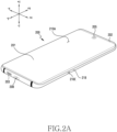
- FIG. 2A is a perspective view illustrating the front side of an electronic device according to an embodiment
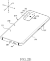
- FIG. 2B is a perspective view illustrating the rear side of the electronic device of FIG. 2A .
- an electronic device 200 may include a housing 210 including a first surface (or a "front surface”) 210A, a second surface (or a “rear surface”) 210B, and a side surface (a "side wall") 210C surrounding a space between the first surface 210A and the second surface 210B.
- the term "housing 210" may refer to a structure defining a part of the first surface 210A, the second surface 210B, and the side surface 210C of FIGS. 2A and 2B .
- the first surface 210A may be defined by a substantially transparent front plate 202 (e.g., a glass plate or a polymer plate including various coating layers).
- the front plate 202 may include a curved portion bent and seamlessly extending from the first surface 210A toward the rear plate 211 in at least one side edge portion.
- the second surface 210B may be defined by a substantially opaque rear plate 211.
- the rear plate 211 may be made of, for example, coated or colored glass, ceramic, polymer, or metal (e.g., aluminum, stainless steel (STS), or magnesium), or a combination of two or more of these materials.
- the rear plate 211 may include a curved portion bent and extending seamlessly from the second surface 210B towards the front plate 202 in at least one side edge portion.
- the side surface 210C may be defined by a side member (or a "bracket") 218 coupled to the front plate 202 and the rear plate 211 and including a metal and/or a polymer.
- the rear plate 211 and the side member 218 may be configured in an integral structure, and may include the same material (e.g., a metal material such as aluminum).
- the electronic device 200 may include at least one of a display 201, an audio module 203, a sensor module (not illustrated), camera modules 205, 212, 213, and 206, a key input device 217, and a connector hole 208.
- at least one of the components e.g., the key input devices 217) may be omitted, or other components may be additionally included.
- the electronic device 200 may include a sensor module (not illustrated).
- a sensor such as a proximity sensor or an illuminance sensor, may be integrated into the display 201 or disposed at a position adjacent to the display 201.
- the electronic device 200 may further include a light-emitting element, and the light-emitting element may be disposed at a position adjacent to the display 201 in the region provided by the front plate 202.
- the light-emitting element may provide, for example, the state information of the electronic device 200 in an optical form.
- the light-emitting element may provide, for example, a light source that is interlocked with the operation of the camera module 205.
- the light-emitting element may include, for example, an LED, an IR LED, and a xenon lamp.
- the display 201 may be visible to the outside of the electronic device 200 through, for example, a substantial portion of the front plate 202.
- the edges of the display 201 may be substantially the same as the shape of the outer periphery (e.g., a curved surface) of the front plate 202 adjacent thereto.
- the distance between the outer periphery of the display 201 and the outer periphery of the front plate 202 may be substantially constant in order to enlarge the exposed area of the display 201.
- a recess or an opening may be provided in a portion of a screen display region of the display 201, and other electronic components aligned with the recess or the opening, such as the camera module 205, a proximity sensor (not illustrated), or an illuminance sensor (not illustrated), may be included.
- the rear surface of the screen display region of the display 201 may include at least one of the camera modules 212, 213, 214, and 215, a fingerprint sensor, and a flash (e.g., 206).
- the display 201 may be coupled to or disposed adjacent to a touch-sensitive circuit, a pressure sensor capable of measuring a touch intensity (pressure), and/or a digitizer configured to detect an electromagnetic field-type stylus pen.
- the audio module 203 may include a microphone hole and a speaker hole.
- the microphone hole may include a microphone disposed therein so as to acquire external sound. In some embodiments, multiple microphones may be disposed so as to detect the direction of sound.
- the speaker hole and the microphone hole may be implemented as a single hole 203, or a speaker (e.g., a piezo speaker) may be included without a speaker hole.
- the speaker hole may include an external speaker hole and a call receiver hole.
- the electronic device 200 may generate an electrical signal or data value corresponding to an internal operating state or an external environmental condition.
- the sensor module may further include, for example, a proximity sensor disposed on the first surface 210A of the housing 210, a fingerprint sensor incorporated in or disposed adjacent to the display 201, and/or a biometric sensor (e.g., an HRM sensor) disposed on the second surface 210B of the housing 210.
- the electronic device 200 may further include at least one of sensor modules (not illustrated), such as a gesture sensor, a gyro sensor, an atmospheric pressure sensor, a magnetic sensor, an acceleration sensor, a grip sensor, a color sensor, an infrared (IR) sensor, a biometric sensor, a temperature sensor, a humidity sensor, or an illuminance sensor.
- sensor modules such as a gesture sensor, a gyro sensor, an atmospheric pressure sensor, a magnetic sensor, an acceleration sensor, a grip sensor, a color sensor, an infrared (IR) sensor, a biometric sensor, a temperature sensor, a humidity sensor, or an illuminance sensor.
- the camera modules 205, 212, 213, 214, 215, and 206 may include a first camera device 205 disposed on the first surface 210A of the electronic device 200, second camera devices 212, 213, 214, and 215 disposed on the second surface 210B thereof, and/or a flash 206.
- the above-described camera modules 205, 212, 213, 214, and 215 may include one or more lenses, an image sensor, and/or an image signal processor.
- the flash 206 may include, for example, a light-emitting diode or a xenon lamp.
- two or more lenses e.g., an infrared camera lens, a wide-angle lens, and a telephoto lens
- image sensors may be disposed on one surface of the electronic device 200.
- the key input devices 217 may be disposed on the side surface 210C of the housing 210.
- the electronic device 200 may not include some or all of the above-mentioned key input devices 217, and a key input device 217, which is not included in the electronic device 100, may be implemented in another form, such as a soft key, on the display 201.
- the key input devices may include a fingerprint sensor disposed on the second surface 210B of the housing 210.
- the connector hole 208 may accommodate a connector configured to transmit and receive power and/or data to and from an external electronic device and a connector configured to transmit and receive an audio signal to and from an external electronic device.
- the connector hole 208 may include a USB connector or an earphone jack.
- the USB connector and the earphone jack may be implemented as a single hole (e.g., 208 in FIGS. 2A and 2B ), and according to another embodiment (not illustrated), the electronic device 200 may transmit/receive power and/or data or transmit/or receive an audio signal to/from an external electronic device (e.g., the electronic devices 102 and 104 in FIG. 1 ) without a separate connector hole.
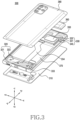
- FIG. 3 is an exploded perspective view of an electronic device according to an embodiment.
- an electronic device 300 may include a front plate (not illustrated) (e.g., the front plate 202 in FIG. 2A ), a display 310 (e.g., the display 201 in FIG. 2A ), a side member 320 (e.g., the side member 218 in FIGS. 2A and 2B ), a printed circuit board structure 330, a shield structure 350, a rear case 360, a battery 370, and/or a rear plate 380.
- At least one of the components of the electronic device 300 according to an embodiment may be the same as or similar to at least one of the components of the electronic device 101 of FIG. 1 and/or the electronic device 200 of FIGS. 2A and 2B , and redundant descriptions thereof will be omitted below.
- the side member 320 is positioned between the display 310 and the back plate 380 and may include a metal frame structure 321 and/or a support member 322.
- the metal frame structure 321 of the side member 320 may be formed of a conductive material (e.g., metal) to provide the side surface of the electronic device 300 (e.g., the side surface 210C in FIG. 2A ).
- the metal frame structure 321 may include at least one conductive portion and/or at least one non-conductive portion that insulates the at least one conductive portion.
- the at least one conductive portion of the metal frame structure 321 may operate as an antenna radiator for transmitting and/or receiving an RF signal of a predetermined frequency band.
- the support member 322 of the side member 320 may be formed of a metal material and/or a non-metal (e.g., polymer) material to provide a space (or a "mounting space") that allows electronic components to be disposed in the electronic device 300.
- the display 310 may be disposed on one surface of the support member 322 (e.g., the surface in the +z direction in FIG. 3 ), and the printed circuit board structure 330 may be disposed on the other surface of the support structure 412 (e.g., the surface in the -z direction in FIG. 3 ).
- the support member 332 may be connected to the metal frame structure 321 or may be configured integrally with the metal frame structure 321.
- the printed circuit board structure 330 may be disposed in at least one region of the support member 332, and the above-described printed circuit board structure 330 may be a structure in which a plurality of printed circuit boards 331 and 332 are stacked.
- the printed circuit board structure 330 may include a first printed circuit board 331, a second printed circuit board 332, and/or an interposer 340.
- the above-described printed circuit board structure 330 may be a structure in which the interposer 340 and the second printed circuit board 332 are stacked in this order with reference to the first printed circuit board 331.
- the first printed circuit board 331 may be disposed on the support member 332, and the second printed circuit board 332 may be spaced apart from the first printed circuit board 331 to be located in the -z direction with reference to the first printed circuit board 331.
- the interposer 340 may be interposed between the first printed circuit board 331 and the second printed circuit board 332 to support the second printed circuit board 332 located in the -z direction on the first printed circuit board 331.
- the interposer 340 may include at least one side wall and/or at least one conductive via penetrating at least one region of the side wall.
- the first printed circuit board 331 located at the bottom of the interposer 340 e.g., the +z direction in FIG. 3
- the second printed circuit board 332 located at the top of the interposer 340 may be electrically connected to each other through at least one via in the interposer 340.
- a plurality of electronic components may be disposed on the first printed circuit board 331 and/or the second printed circuit board 332 constituting the printed circuit board structure 330.
- a processor e.g., the processor 120 in FIG. 1
- a memory e.g., the memory 130 in FIG. 1
- an interface e.g., the interface 177 in FIG. 1
- the processor may include, for example, at least one of a central processing unit, an application processor, a graphics processing unit, an image signal processor, a sensor hub processor, or a communication processor.
- the memory may include, for example, a volatile memory or a non-volatile memory.
- the interface may include, for example, a high-definition multimedia interface (HDMI), a universal serial bus (USB) interface, an SD card interface, and/or an audio interface.
- HDMI high-definition multimedia interface
- USB universal serial bus
- the interface may electrically or physically connect, for example, the electronic device 200 to an external electronic device, and may include a USB connector, an SD card/an MMC connector, or an audio connector.
- the plurality of electronic components disposed on the first printed circuit board 331 and the plurality of electronic components disposed on the second printed circuit board 332 may be electrically and/or operatively connected to each other via the interposer 340.
- the first printed circuit board 331 and/or the second printed circuit board 332 of the printed circuit board structure 330 may be electrically connected to a third printed circuit board 333 which is disposed to be spaced apart from the printed circuit board structure 330.
- the first printed circuit board 331 and/or the second printed circuit board 332 of the printed circuit board structure 330 may be disposed in a region of the support member 322 (e.g., a region in the +y-direction in FIG. 3 ), and the third printed circuit board 333 may be disposed in another region of the support member 332 spaced apart from the first printed circuit board 331 and/or the second printed circuit board 332 (e.g., in the -y direction in FIG. 3 ).
- the first printed circuit board 331 and/or the second printed circuit board 332 may be electrically connected to the third printed circuit board 333 via an electrical connection member 334.
- the electrical connection member 334 may electrically interconnect the first printed circuit board 331 and/or the second printed circuit board 332 and the third printed circuit 333 across the battery 370 disposed on the support member 322.
- the electrical connection member 334 may include at least one of a flexible printed circuit board (FPCB), a coaxial cable, and a board to board connector (a B to B connector), but is limited thereto.
- the shield structure 350 may be formed of a conductive material (e.g., metal), and may be disposed in at least one region of the printed circuit board structure 330 to electromagnetically shield as plurality of electronic components disposed on the printed circuit board structure 330.
- the shield structure 350 may be disposed on the second printed circuit board 332 of the printed circuit board structure 330, and may electromagnetically shield a plurality of electronic components disposed on the second printed circuit board 332.
- the shield structure 350 may include an extension (not illustrated) fixed to at least one region of the first printed circuit board 331 and/or the second printed circuit board 332 in order to secure the structural rigidity of the printed circuit board structure 330. A description of the extension of the shield structure 350 will be described later.
- the rear case 360 may be disposed on the -z direction of the printed circuit board structure 330 to protect the first printed circuit board 331 and /or the second printed circuit board 332 and the plurality of electronic components disposed on the first printed circuit board 331 and/or the second printed circuit board 332 from an external force applied to the electronic device 300.
- the rear case 360 may be formed of a non-conductive material (e.g., plastic), but is not limited thereto.
- the rear case 360 may be omitted.
- the battery 370 may be disposed inside the electronic device 300 to supply power to at least one component of the electronic device 300.
- the battery 370 may include, for example, a non-rechargeable primary cell, a rechargeable secondary cell, or a fuel cell.
- the battery 370 may be disposed in a battery groove (not illustrated) provided in at least one region of the support member 322 to supply power to components of the electronic device 300.
- the battery 370 may be integrally disposed inside the electronic device 300, but is not limited thereto.
- a battery 370 according to another embodiment may be detachably disposed on the electronic device 300.
- the rear plate 380 may define the rear surface of the electronic device 300 (e.g., the second surface 210B in FIG. 2B ).
- the rear plate 380 may protect the internal components of the electronic device 300 from an external impact or inflow of foreign substances.
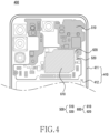
- FIG. 4 is a view illustrating a side member of an electronic device according to an embodiment and a printed circuit board structure disposed on the side member
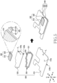
- FIG. 5 is an exploded view illustrating a printed circuit board structure and a shield structure of an electronic device according to an embodiment
- FIG. 6 is an exploded view illustrating a printed circuit board structure and a shield structure of an electronic device according to another embodiment.
- FIG. 4 illustrates a partial region (e.g., a region in the +y direction in FIG. 4 ) of the side member 410 of the electronic device 400.
- the electronic device 400 (the electronic device 300 in FIG. 3 ) according to an embodiment may include a side member 410 (e.g., the side member 320 in FIG. 3 ), a printed circuit board structure 500 (e.g., the printed circuit board structure 500 in FIG. 3 ), and/or a shield structure 600 (e.g., the shield structure 350 in FIG. 3 ).
- a side member 410 e.g., the side member 320 in FIG. 3
- a printed circuit board structure 500 e.g., the printed circuit board structure 500 in FIG. 3
- a shield structure 600 e.g., the shield structure 350 in FIG. 3
- At least one of the components of the electronic device 400 according to an embodiment may be the same as or similar to at least one of the components of the electronic device 300 of FIG. 3 , and redundant descriptions will be omitted below.
- the side member 410 may include a metal frame structure 411 (e.g., the metal frame structure 321 in FIG. 3 ) and/or a support member 412 (e.g., the support member 322 in FIG. 3 ).
- the metal frame structure 411 of the side member 410 may define a side surface (e.g., the side surface 210C in FIG. 2A ) of the electronic device 400.
- the support member 412 of the side member 410 may provide a space (or a "mounting space") in which components of the electronic device 400 (e.g., the printed circuit board structure 500) may be disposed.
- the printed circuit board structure 500 may be disposed in at least one region of the support member 412, and the printed circuit board structure 500 may include a first printed circuit board 510 (e.g., the first printed circuit board 331 in FIG. 3 ), a second printed circuit board 520 (e.g., the second printed circuit board 332 in FIG. 3 ), and/or an interposer 530 (e.g., the interposer 340 in FIG. 3 ).
- a first printed circuit board 510 e.g., the first printed circuit board 331 in FIG. 3
- a second printed circuit board 520 e.g., the second printed circuit board 332 in FIG. 3
- an interposer 530 e.g., the interposer 340 in FIG. 3
- the printed circuit board structure 500 may be a structure in which the interposer 530 and the second printed circuit board 520 are stacked in this order with reference to the first printed circuit board 510.
- the first printed circuit board 510 may include a first surface 510a facing a first direction (e.g., the +z direction in FIGS. 5 and 6 ) and a second surface 510b facing a second direction (e.g., the -z direction in FIGS. 5 and 6 ) opposite to the first direction.
- the second printed circuit board 520 is spaced apart from the first printed circuit board 510 and may include a third surface 520a facing the first direction and a fourth surface 520b facing a second direction opposite to the third surface 520a and facing the first surface 510a of the first printed circuit board 510.
- the interposer 530 may be interposed between the first surface 510a of the first printed circuit board 510 and the fourth surface 520b of the second printed circuit board 520, and the second printed circuit board 520 may be stacked at the top of the first printed circuit board 510 (e.g., in the +z direction in FIG. 5 ) via the above-described interposer 530.
- a first solder pad may be located in at least one region of the interposer 530 facing the first printed circuit board 510, and a (1-1) th solder pad (not illustrated) may be located in at least one region of the first printed circuit board 510 facing the interposer 530.
- a second solder pad may be located in at least one region of the interposer 530 facing the second printed circuit board 520, and a (2-1) th solder pad (not illustrated) may be located in at least one region of the second printed circuit board 520 facing the interposer 530.
- the first printed circuit board 510 and the interposer 530 may be physically connected or fixed to each other.
- the second solder pad and the (2-1) th solder pad are soldered to each other, the second printed circuit board 520 and the interposer 530 may be physically connected or fixed to each other.
- the first printed circuit board 510 may be disposed at the bottom of the interposer 530 (e.g., in the -z direction in FIGS. 5 and 6 )
- the second printed circuit board 520 may be stacked at the top of the interposer 530 (e.g., in the +z direction in FIGS. 5 and 6 ).
- the interposer 530 may include at least one side wall 531 and/or at least one via 532.
- the at least one side wall 531 may include at least one through hole (not illustrated) and extend along an edge of the second printed circuit board 520 disposed at the top of the interposer 530 (e.g., in the +z direction in FIG. 5 ).
- the at least one side wall 531 may have a band-like closed curve shape corresponding to the edge shape of the second printed circuit board 520, but is not limited thereto.
- the at least one via 532 may be formed of a conductive material, and may be located in the at least one through hole to electrically interconnect the first printed circuit board 510 disposed at the bottom of the interposer 530 (e.g., in the -z direction in FIG. 5 ) and the second printed circuit board 520 disposed at the top of the interposer 530 (e.g., the +z direction in FIG. 5 ).
- the shield structure 600 may be disposed in at least one region of the third surface 520a of the second printed circuit board 520 to electromagnetically shield a plurality of electronic components disposed in the second printed circuit board 520.
- the shield structure 600 may prevent noise generated from other components of the electronic device 400 from flowing into the plurality of electronic components disposed on the second printed circuit board 520.
- the shield structure 600 may block noise generated from the plurality of electronic components disposed on the second printed circuit board 520 from flowing out to the outside.
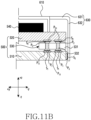
- the shield structure 600 may include a body 610 and/or a first extension 620 extending from at least one region of the body 610, and the shield structure 600 may increase the physical connection strength of the printed circuit board structure 500 by the first extension 620.
- the body 610 of the shield structure 600 may be disposed on at least one region of the third surface 520a of the second printed circuit board 520. In another example, the body 610 may be disposed in a shape that surrounds the plurality of electronic components disposed on the second printed circuit board 520 to electromagnetically shield the plurality of electronic components disposed on the second printed circuit board 520.
- the first extension 620 of the shield structure 600 may be protrude from one region of the body 610 described above.
- the first extension 620 may protrude, for example, in a third direction (e.g., the +x direction in FIGS. 5 and 6 ) substantially perpendicular to the first direction with reference to the body 610, but is not limited thereto.
- the first extension 620 may protrude in a fourth direction (e.g., the -y direction and/or the +y direction in FIGS. 5 and 6 ) substantially perpendicular to the first direction with reference to the body 610.
- the first extension 620 of the shield structure 600 may extend up to at least one region (e.g., the first surface 510a) of the first printed circuit board 510 from the body 610.
- One region of the above-described first extension 620 may be fixed to at least one region of the first printed circuit board 510 and/or the second printed circuit board 520 and reinforce the physical connection strength of the printed circuit board structure 500.
- the first extension 620 may be configured in a surface-mounted device (SMD) form (or a "surface-mounted component form") and increase the physical connection strength of the first printed circuit board 510, the interposer 530, and/or the second printed circuit board 520.
- the first extension 620 may include a first portion 621 protruding from one region of the body 610, a second portion 622 connected to one end (e.g., the end in the +x direction in FIG. 5 ) of the first portion 621 substantially perpendicular to the first portion 621, and/or a third portion 623 connected to one end (e.g., the end in the -z direction in FIG. 5 ) of the second portion 622 substantially perpendicular to the second portion 622.
- SMD surface-mounted device
- the first portion 621 of the first extension 620 may protrude from at least one region of the body 610 in a third direction (e.g., the +x direction in FIG. 5 ).
- the first portion 621 may be disposed adjacent to the third surface 520a of the second printed circuit board 520, and at least one region of the first portion 621 may be fixed to the third surface 520a of the second printed circuit board 520.
- at least one region of the first portion 621 may be soldered to a third solder pad P 3 disposed on the third surface 520a of the second printed circuit board 520, but is not limited thereto.
- soldering may refer to a process of applying heat to solder to fix some components (e.g., the first portion 621) to a specific location (e.g., the third surface 520a of the second printed circuit board 520), and may be used in an overlapping sense in the following.
- the second portion 622 of the first extension 620 may extend along a second direction (e.g., the -z direction in FIG. 5 ) perpendicular to the first portion 621 from one end (e.g., the end in the +x direction in FIG. 5 ) of the first portion 621.
- the second portion 622 may be disposed to be spaced apart from the second printed circuit board 520 and/or the interposer 530.
- the second portion 622 may be disposed to face one surface of the second printed circuit board 520 and/or one surface of the interposer 530 facing the third direction (e.g., the +x direction in FIG. 5 ).
- the third portion 623 of the first extension 620 may extend along the third direction (e.g., the +x direction in FIG. 5 ) substantially perpendicular to the second portion 622 from one end of the second portion 622 facing the first surface 510a of the first printed circuit board 510.
- the third portion 623 may be disposed adjacent to the first surface 510a of the first printed circuit board 510, and at least one region of the third portion 623 may be fixed to the first surface 510a of the first printed circuit board 510.
- at least one region of the third portion 623 may be soldered to a fourth solder pad P 4 disposed on the first surface 5 10a of the first printed circuit board 510, but is not limited thereto.
- the first extension 620 may interconnect the first printed circuit board 510 and the second printed circuit board 520 via the first portion 621 fixed to the third surface 520a of the second printed circuit board 520, the third portion 623 fixed to the first surface 510a of the first printed circuit board 510, and/or the second portion 622 connecting the first portion 621 and the third portion 623. That is, the first extension 620 may increase the physical connection strength between the first printed circuit board 510, the interposer 530, and/or the second printed circuit board 520 by providing a connection structure between the above-described first printed circuit board 510 and second printed circuit board 520.
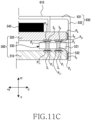
- At least one region of the first extension 620 may be configured in a pin shape (e.g., a dual in-line package (DIP) pin).
- the above-described first extension 620 may be inserted into at least one hole 5111 provided in at least one region of the first printed circuit board 510 to be fixed to at least one region of the first printed circuit board 510.
- the first extension 620 may include a first portion 621 protruding from one region of the body 610, a second portion 622 connected to one end (e.g., the end in the +x direction in FIG.
- first portion 621 and substantially perpendicular to the first portion 621, and/or a third portion 623 connected to one end (e.g., the end in the -z direction in FIG. 5 ) of the second portion 622 and inserted into at least one region of the first printed circuit board 510.
- the first portion 621 of the first extension 620 may protrude from at least one region of the body 610 in a third direction (e.g., the +x direction in FIG. 6 ).
- the first portion 621 may be disposed adjacent to the third surface 520a of the second printed circuit board 520, and at least one region of the first portion 621 may be fixed to the third surface 520a of the second printed circuit board 520.
- at least one region of the first portion 621 may be soldered to a third solder pad P 3 disposed on the third surface 520a of the second printed circuit board 520, but is not limited thereto.
- the second portion 622 of the first extension 620 may extend along a second direction (e.g., the -z direction in FIG. 6 ) perpendicular to the first portion 621 from one end (e.g., the end in the +x direction in FIG. 6 ) of the first portion 621.
- the second portion 622 may be disposed to be spaced apart from the second printed circuit board 520 and/or the interposer 530.
- the second portion 622 may be disposed to face one surface of the second printed circuit board 520 and/or one surface of the interposer 530 facing the third direction (e.g., the +x direction in FIG. 6 ).
- the third portion 623 of the first extension 620 may extend from one end of the second portion 622 facing the first surface 510a of the first printed circuit board 510.
- the third portion 623 may extend in the second direction (e.g., the -z direction in FIG. 6 ) with reference to the above-mentioned one end of the second portion 622, but is not limited thereto.
- the third portion 623 may be inserted into at least one region of the first printed circuit board 510 and fixed to the at least one region of the first printed circuit board 510.
- At least one hole 5111 may be provided in the first surface 510a of the first printed circuit board 510, and the third portion 623 may be inserted into the at least one hole 5111 to be fixed to the first printed circuit board 510.
- the third portion 623 may be fixed to the first printed circuit board 510 by being soldered to the fourth solder pad P 4 disposed around the at least one hole 5111 in the state of being inserted into the at least one hole 5111 of the first printed circuit board 510, but is not limited thereto.
- the at least one hole 5111 may be provided in a shape surrounding the outer circumferential surface of the third portion 623, and the fourth solder pad P 4 may be disposed in a shape surrounding the at least one hole 5111, but is not limited thereto.
- the first extension 620 may interconnect the first printed circuit board 510 and the second printed circuit board 520 via the first portion 621 fixed to the third surface 520a of the second printed circuit board 520, the third portion 623 fixedly inserted into the first printed circuit board 510, and/or the second portion 622 connecting the first portion 621 and the third portion 623. That is, the first extension 620 may increase the physical connection strength between the first printed circuit board 510, the interposer 530, and/or the second printed circuit board 520 by providing a connection structure between the above-described first printed circuit board 510 and second printed circuit board 520.
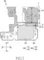
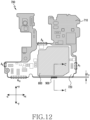
- FIG. 7 is a front view illustrating a printed circuit board structure of an electronic device according to an embodiment.
- FIG. 7 illustrates a printed circuit board structure 500 and/or a shield structure 600 disposed inside an electronic device (e.g., the electronic device 400 in FIG. 4 ).
- an electronic device (e.g., the electronic device 400 in FIG. 4 ) may include a printed circuit board structure 500 (e.g., the printed circuit board structure 500 in FIGS. 5 and 6 ) and/or a shield structure 600 (e.g., the printed circuit board structure 500 in FIGS. 5 and 6 ).
- a printed circuit board structure 500 e.g., the printed circuit board structure 500 in FIGS. 5 and 6
- a shield structure 600 e.g., the printed circuit board structure 500 in FIGS. 5 and 6 .
- the printed circuit board structure 500 may include a first printed circuit board 510 (e.g., the first printed circuit board 510 in FIGS. 5 and 6 ) and a second printed circuit board 520 stacked on the first printed circuit board 510.
- the second printed circuit board 520 may be stacked on the first printed circuit board 510 via an interposer (not illustrated) disposed on at least one region of the first printed circuit board 510 (e.g., the interposer 530 in FIGS. 5 and 6 ).
- the first printed circuit board 510 and the second printed circuit board 520 may be electrically interconnected via an interposer interposed between the first printed circuit board 510 and the second printed circuit board 520.
- the area of the first printed circuit board 510 when viewed from the top of the printed circuit board structure 500 (e.g., in the +z direction in FIGS. 5 and 6 ), the area of the first printed circuit board 510 may be greater than the area of the second printed circuit board 520.
- the second printed circuit board 520 may be located inside a closed curve formed by the edges of the first printed circuit board 510.
- the second printed circuit board 520 may be disposed such that the outer peripheral surface of the second printed circuit board 520 is included in the outer peripheral surface of the first printed circuit board 510 when viewed from the top of the printed circuit board structure 500 (e.g., in the +z direction in FIGS. 5 and 6 ).
- the second printed circuit board 520 may be disposed such that a partial region of the second printed circuit board 520 overlaps the first printed circuit board 510 while the remaining region does not overlap the first printed circuit board 510 when viewed from the top of the printed circuit board structure 500.
- the shield structure 600 may be located in at least one region of the second printed circuit board 520 of the printed circuit board structure 500 to shield a plurality of electronic components disposed in the at least one region of the second printed circuit board 520 (e.g., the third surface 520a in FIGS. 5 and 6 ).
- the shield structure 600 may include a body 610 (e.g., the body 610 in FIG. 5 and/or FIG. 6 ) fixed to the second printed circuit board 520 and/or a first extension 620 (e.g., the first extension 620 in FIG. 5 and/or FIG. 6 ) extending from the body 610.
- the first extension 620 of the shield structure 600 may be fixed to at least one region of the first printed circuit board 510 and/or at least one region of the second printed circuit board 520 to provide a connection structure between the first printed circuit board 510 and the second printed circuit board 520.
- the first extension 620 of the shield structure 600 may be provided in a region in which the distance between an edge of the first printed circuit board 510 and an edge of the second printed circuit board 520 located inside the edge of the first printed circuit board 510 is equal to or greater than a predetermined distance (e.g., L 1 in FIG. 7 ).
- the predetermined distance may mean, for example, a distance in which a rigidity reinforcement effect may be obtained when a partial region of the first extension 620 is fixed or soldered to a region of the first printed circuit board 510.
- the first extension 620 of the shield structure 600 may be provided in a region in which the distance between an edge of the first printed circuit board 510 and an edge of the second printed circuit board 520 is the greatest (e.g., the region A 1 in FIG. 7 ), but is not limited thereto.
- an electronic device e.g., the electronic device 300 of FIG. 3 or the electronic device 400 of FIG. 4
- a relatively large amount of warpage may be generated in a region in which the distance between an edge of the first printed circuit board 510 and an edge of the second printed circuit board 520 is equal to or greater than the predetermined distance L- 1 (e.g., the region F in FIG. 7 ) compared to other regions.
- an impact e.g., bending stress
- the interposer e.g., the interposer 530 in FIGS. 5 and 6
- the second printed circuit board 520 By the impact transferred to the region in which the first printed circuit board 510, the interposer 530 and/or the second printed circuit board 520 are stacked, the soldering for connecting or fixing the first printed circuit board 510, the second printed circuit board 520, and/or the interposer may be fractured, or the connection between the first printed circuit board 510, the second printed circuit board 520, and/or the interposer 530 may be separated.
- the first extension 620 of the shield structure 600 may be located in the region in which the distance between an edge of the first printed circuit board 510 and an edge of the second printed circuit board 520 is equal to or greater than a predetermine distance L- 1 (e.g., the region F in FIG. 7 ), and may provide a connection structure between the first printed circuit board 510 and the second printed circuit board 520.
- L- 1 e.g., the region F in FIG. 7
- the physical connection strength or rigidity between the first printed circuit board 510, the interposer 530, and/or the second printed circuit board 520 may be increased by the first extension 620 of the above-described shield structure 600, and as a result, damage to the printed circuit board structure 500 caused by the warpage of the first printed circuit board 510 and/or the second printed circuit board 520 may be reduced.
- the structure of the first extension 620 will be described in detail with reference to FIGS. 8 and 9 .
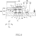
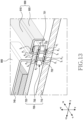
- FIG. 8 is a cross-sectional perspective view illustrating the printed circuit board structure of FIG. 7 cut in A-A' direction
- FIG. 9 is a side view illustrating the printed circuit board structure of FIG. 8
- FIG. 9 is a view of the printed circuit board structure 500 of FIG. 8 obtained when viewed in the -y direction (e.g., the -y direction in FIG. 8 ).
- the structure of the first extension 620 is not limited to the illustrated embodiment.
- the first extension 620 of the shield structure 600 may be provided in the form of a pin (e.g., a dual in-line package (DIP) pin).
- DIP dual in-line package
- an electronic device may include a printed circuit board structure 500 (e.g., the printed circuit board structure in FIGS. 5 and 6 ) and/or a shield structure 600 (e.g., the shield structure 600 in FIGS. 5 and 6 ).
- the printed circuit board structure 500 and/or the shield structure 600 of FIGS. 8 and 9 may be substantially the same as or similar to the printed circuit board structure 500 and/or the shield structure 600 in FIG. 5 and/or FIG. 6 , and redundant descriptions will be omitted below.
- the printed circuit board structure 500 may include a first printed circuit board 510 (e.g., the first printed circuit board 510 in FIGS. 5 and 6 ), a second printed circuit board 520 (e.g., the second printed circuit board 520 in FIGS. 5 and 6 ), and/or an interposer 530 (e.g., the interposer 530 in FIGS. 5 and 6 ).
- the printed circuit board structure 500 may be a structure in which an interposer 530 and a second printed circuit board 520 are stacked in this order at the top (e.g., in the +z direction in FIGS. 8 and 9 ) with reference to the first printed circuit board 510.
- the interposer 530 may include at least one side wall 531 (e.g., the at least one side wall 531 in FIGS. 5 and 6 ) extending along at least one edge of the second printed circuit board 520 and/or at least one via 532 (e.g., the at least one via 532 in FIGS. 5 and 6 ) including a conductive material.
- at least one through hole (not illustrated) may be provided in the at least one side wall 531, and the at least one via 532 may be disposed in the at least one through hole to penetrate the at least one side wall 531.
- first printed circuit board 510 disposed at the top of the interposer 530 (e.g., in the +z direction) and the second printed circuit 520 disposed at the bottom (e.g., in the -z direction) of the interposer 530 may be electrically interconnected via the at least one via 532.
- the first printed circuit board 510 is fixed to at least one region of the bottom surface (e.g., the surface in the -z direction in FIGS. 8 and 9 ) of the interposer 530
- the second printed circuit board 520 may be fixed to at least one region of the top surface (e.g., the surface in the +z direction in FIGS. 8 and 9 ) of the interposer 530.
- the first printed circuit board 510 may be fixed to at least one region of the bottom surface of the interposer 530.
- a first solder region S 1 may be provided between the top surface (e.g., the first surface 510a in FIGS. 5 and 6 ) of the first printed circuit board 510 and the bottom surface of the interposer 530.
- a first solder region S 1 may be provided between the top surface (e.g., the first surface 510a in FIGS. 5 and 6 ) of the first printed circuit board 510 and the bottom surface of the interposer 530.
- the second solder pad P 2 disposed on the top surface of the interposer 530 and a (2-1) th solder pad P 21 disposed on the bottom surface of the second printed circuit board 520 are soldered to each other, the second printed circuit board 520 may be fixed to the top surface of the interposer 530.
- the bottom surface e.g., the fourth surface 510b in FIGS.
- the printed circuit board structure 500 may increase the physical connection strength between the first printed circuit board 510, the interposer 530, and/or the second printed circuit board 520 by the first solder region S 1 provided between the first printed circuit board 510 and the interposer 530 and the second solder region S 2 provided between the second printed circuit board 520 and the interposer 530.
- the shield structure 600 may include a body 610 disposed in at least one region of the second printed circuit board 520 and/or a first extension 620 extending from the body 610 and connecting the first printed circuit board 510 and the second printed circuit board 520.
- the body 610 of the shield structure 600 may be disposed on the top surface (e.g., the third surface 520a in FIGS. 5 and 6 ) of the second printed circuit board 520, and may electromagnetically shield at least one electronic component (not illustrated) (e.g., the wireless communication module 192 in FIG. 1 ) disposed on the second printed circuit board 520.
- the body 610 may block external noise introduced into the at least one electronic component disposed on the second printed circuit board 520.
- the first extension 620 of the shield structure 600 may protrude from at least one region of the body 610, and may serve to physically interconnect the first printed circuit board 510 and the second printed circuit board 520.
- the first extension 620 may include a first portion 621, a second portion 622, and/or a third portion 623.
- the above-described first extension 620 may interconnect the first printed circuit board 510 and the second printed circuit board 520 by the first portion 621, the second portion 622, and/or the third portion 623, whereby it is possible to improve or reinforce the physical connection strength of the printed circuit board structure 500.
- the first portion 621 of the first extension 620 may be protrude from one region of the body 610.
- the first portion 621 may extend in the +x direction with reference to the body 610.
- a partial region of the first portion 621 may overlap at least one region of the second printed circuit board 520 and the remaining region of the first portion 621 may overlap with at least one region of the first printed circuit board 510.
- at least one region of the first portion 621 may be fixed to at least one region of the second printed circuit board 520.
- At least one region of the first portion 621 may be fixed to the second printed circuit board by being soldered to a third solder pad P 3 (e.g., the third solder pad P 3 in FIG. 5 ) disposed on the top surface (the surface facing the +z direction in FIGS. 8 and 9 ) of the second printed circuit board 520.
- a third solder region S 3 may be provided between the first portion 621 of the first extension 620 and the third solder pad P 3 of the second printed circuit board 520.
- the second portion 622 of the first extension 620 may be connected to one end (e.g., the end in the +x direction in FIGS. 8 and 9 ) of the first portion 621, and may extend in a direction substantially perpendicular to the first portion 621 (e.g., the -z direction in FIGS. 8 and 9 ).
- the second portion 622 may extend from one end of the first portion 621 by a length corresponding to the sum of the height of the second printed circuit board 520, the height of the interposer 530, and the height of the first solder pad Pi, the height of the second solder pad P 2 , the first solder region S 1 , and/or the second solder region S 2 , but is not limited thereto.
- the second portion 622 may be disposed adjacent to the second printed circuit board 520 and/or the interposer 530, wherein at least one region of the second portion 622 may face one surface of the second printed circuit substrate 520 and/or one surface of the interposer 530 facing the +x direction.
- the third portion 622 of the first extension 620 may be connected to one end (e.g., the end in the -z direction in FIGS. 8 and 9 ) of the second portion 622, and may extend in a direction substantially perpendicular to the second portion 622 (e.g., the +x direction in FIGS. 8 and 9 ).
- the third portion 622 may be disposed to be in contact with the top surface of the first printed circuit board 510 (e.g., the surface in the +z direction in FIGS. 8 and 9 ), and at least one region of the third portion 623 may be fixed to at least one region of the first printed circuit board 510.
- At least one region of the third portion 623 may be fixed to the first printed circuit board 510 by being soldered to a fourth solder pad P 4 (e.g., the fourth solder pad P 4 in FIG. 5 ) disposed on the top surface of the first printed circuit board 510.
- a fourth solder region S 4 may be provided between the third portion 623 of the first extension 620 and the fourth solder pad P 4 of the first printed circuit board 510.
- the shield structure 600 may interconnect the first printed circuit board 510 and the second printed circuit board 520 via the first extension 620 including the first portion 621 fixed to the second printed circuit board 520, the third portion 623 fixed to the first printed circuit board 510, and/or the second portion 622 connecting the first portion 621 and the third portion 623.
- the shield structure 600 may reinforce or increase the physical connection strength between the first printed circuit board 510, the interposer 530, and/or the second printed circuit board 520 by providing a connection structure between the first printed circuit board 510 and second printed circuit board 520 by the above-described first extension 620.
- the electronic device it is possible to increase the physical connection strength of the printed circuit board structure 500 by providing the third solder region S 3 between the first extension 620 and the second printed circuit board 520 and providing the fourth solder region S 4 between the first extension 620 and the first printed circuit board 510, in addition to providing the first solder region S 1 and/or the second solder region S 2 between the first printed circuit board 510, the second printed circuit board 520, and/or the interposer 530.
- the shield structure 600 may disperse an impact (or "stress”), which is applied to the printed circuit board structure 500 by an external force, to the body 610 thereof via the first extension 620, whereby the shield structure 600 may reduce the fracture of or damage to the printed circuit board structure 500 due to the external force.
- an impact or "stress”
- warpage may occur in the first printed circuit board 510 and/or the second printed circuit board 520 due to an external force (e.g., F in FIG. 9 ) applied to a region of the first printed circuit board 510. Due to the above-described warpage of the first printed circuit board 510 and/or the second printed circuit board 520, an impact (e.g., bending stress) may be transferred to the region (e.g., the region C in FIG. 9 ) in which the first printed circuit board 510, the interposer 530, and/or the second printed circuit board 520 are stacked.
- F in FIG. 9 an external force
- the impact transferred to the region (the region C) in which the first printed circuit board 510, the interposer 530, and/or the second printed circuit board 520 are stacked may cause damage or fracture of the first printed circuit board 510, the second printed circuit board 520, and/or the interposer 530.
- the shield structure 600 may disperse, to the body 610, the impact transferred to the region (the region C) in which the first printed circuit board 510, the interposer 530, and/or the second printed circuit board 520 are stacked by including the first extension 610 fixed to one region (e.g., the regions S 1 and S 2 ) of the first printed circuit board 510 and/or the second printed circuit board 520 and extending from the body 610 thereof.
- the electronic device it is possible to prevent or reduce damage or fracture of the printed circuit board structure 500 by dispersing an impact, which is applied to the first printed circuit board 510, the interposer 530, and/or the second printed circuit board 520, to the body 610 of the shield structure 600 via the first extension 620 of the shield structure 600.
- FIG. 10A is a front view illustrating a printed circuit board structure of an electronic device according to another embodiment
- FIG. 10B is a front view illustrating a printed circuit board structure of an electronic device according to still another embodiment.
- FIG. 10A and/or FIG. 10B illustrate a printed circuit board structure 500 and/or a shield structure 600 disposed inside an electronic device (e.g., the electronic device 400 in FIG. 4 ).
- an electronic device e.g., the electronic device 400 in FIG. 4
- an electronic device may include a printed circuit board structure 500 (e.g., the printed circuit board structure 500 in FIGS. 4 and 5 ) and/or a shield structure 600 (e.g., the shield structure 600 in FIGS. 4 and 5 ) disposed in at least one region of the printed circuit board structure 500.
- the printed circuit board structure 500 and/or the shield structure 600 of FIG. 10A and/or FIG. 10 may be the same as or similar to the printed circuit board structure 500 and/or the shield structure 600 in FIG. 4 and/or FIG. 5 , and redundant descriptions will be omitted below.
- the printed circuit board structure 500 may include a first printed circuit board 510 (e.g., the first printed circuit board 510 in FIGS. 4 and 5 ), a second printed circuit board 520 (e.g., the second printed circuit board 520 in FIGS. 4 and 5 ) stacked on the first printed circuit board 510, and/or an interposer (not illustrated) (e.g., the interposer 530 in FIG. 5 ) interposed between the first printed circuit board 510 and the second printed circuit board 520 to electrically interconnect the first printed circuit board 510 and the second printed circuit board 520.
- an interposer not illustrated
- the area of the first printed circuit board 510 may be greater than the area of the second printed circuit board 520.
- the second printed circuit board 520 may be located inside a closed curve formed by the edges of the first printed circuit board 510.
- the second printed circuit board 520 may be disposed such that the outer peripheral surface of the second printed circuit board 520 is included in the outer peripheral surface of the first printed circuit board 510 when viewed from the top of the printed circuit board structure 500 (e.g., in the +z direction in FIG. 5 ).
- the second printed circuit board 520 may be disposed such that a partial region of the second printed circuit board 520 overlaps the first printed circuit board 510 while the remaining region does not overlap the first printed circuit board 510 when viewed from the top of the printed circuit board structure 500.
- the shield structure 600 may be disposed in at least one region of the second printed circuit board 520 of the printed circuit board structure 500 and may electromagnetically shield at least one electronic component (e.g., the wireless communication module 192 in FIG. 1 ) disposed on the second printed circuit board 520.
- the shield structure 600 may include an extension region (e.g., the second extension 530 in FIGS. 10A and 10B ) connecting the first printed circuit board 510 and the second printed circuit board 520, and the shield structure 600 may increase the physical connection strength of the printed circuit board structure 500 by the above-described extension region.
- the shield structure 600 may include a body 610 disposed on at least one region of the second printed circuit board 520 (e.g., the body 610 in FIGS. 7 and 8 ), a first extension 620 (e.g., the first extension 620 in FIGS. 7 and 8 ) extending from one region of the body 610, and/or a second extension extending from another region of the body 610.
- the first extension 620 may be omitted, and thus the shield structure 600 may include only the body 610 and the second extension 630.
- the body 610 of the shield structure 600 may be provided to surround at least one region of the second printed circuit board 520, and thus an internal space may be defined between the body 610 and the second printed circuit 520. At least one electronic component may be disposed in the internal space defined between the body 610 and/or the second printed circuit board 520, and the above-described body 610 may electromagnetically shield the at least one electronic component disposed in the internal space.
- the first extension 620 of the shield structure 600 may extend from a region of the body 610, and the above-described first extension 620 may be fixed to at least one region of the first printed circuit board 510 and/or the second printed circuit board 520. In another example, the first extension 620 may be fixed to at least one region of the first printed circuit board 510 and/or the second printed circuit board 520, thereby providing a connection structure between the first printed circuit board 510 and the second printed circuit board 520. According to an embodiment, the first extension 620 may be configured in an SMD form (e.g., see FIG. 5 ) and may be fixed to at least one region of the first printed circuit board 510 and/or the second printed circuit board 520.
- SMD form e.g., see FIG. 5
- the form of the first extension 620 is not limited to the above-described embodiment, and in another embodiment, the first extension 620 may be provided in a DIP form (e.g., see FIG. 6 ) and may be fixed to at least one region of the printed circuit board 510 and/or the second printed circuit board 520. Alternatively, the first extension 620 may be omitted according to an embodiment (e.g., see FIG. 10B ).
- the second extension 630 of the shield structure 600 may extend from another region of the body 610, and the above-described second extension 630 may be fixed to at least one region of the first printed circuit board 510 and/or the second printed circuit board 520.
- the second extension 630 may be disposed to be spaced apart from the first extension 620.
- the second extension 630 may be fixed to at least one region of the first printed circuit board 510 and/or the second printed circuit board 520, thereby providing a connection structure between the first printed circuit board 510 and the second printed circuit board 520.
- the second extension 630 may be fixed to at least one region of the top surface (e.g., the third surface 520a in FIG.
- the second printed circuit board 520 and/or at least one region of a side surface (e.g., the surface in the -y direction in FIG. 10A ) of the first printed circuit board 520, but is not limited thereto.
- the first extension 620 of the shield structure 600 may be provided in a region in which the distance between an edge of the first printed circuit board 510 and an edge of the second printed circuit board 520 located inside the edge of the first printed circuit board 510 is equal to or greater than a first distance (e.g., L 1 in FIG. 10A ).
- the first distance L 1 may refer to, for example, a minimum distance for fixing or soldering a partial region (e.g., the third portion 623 of FIG. 5 ) first extension 620 to one surface (e.g., the first surface 510a in FIG. 5 ) of the first printed circuit board 510.
- the first extension 620 of the shield structure 600 may be provided in a region in which the distance between an edge of the first printed circuit board 510 and an edge of the second printed circuit board 520 is the greatest (e.g., the region A 1 in FIG. 10A ), but is not limited thereto.
- the second extension 630 of the shield structure 600 may be provided in a region in which a second distance between an edge of the first printed circuit board 510 and an edge of the second printed circuit board 520 is equal to or smaller than a second distance L 2 (e.g., the region A 2 , region A 3 , region A 4 , region A 5 , and/or region A 6 in FIGS. 10A and 10B ).
- the second distance L 2 may be a distance shorter than the first distance L 1 .
- at least one region of the second extension 630 may be fixed to at least one region of a side surface (e.g., the surface in the -y direction in FIGS.
- the second extension 630 may be disposed in a region in which the distance between an edge of the first printed circuit board 510 and an edge of the second printed circuit board 520 is relatively short so as to serve interconnect the first printed circuit board 510 and the second printed circuit board 520.
- FIG. 10A and/or FIG. 10B an embodiment in which the second extension 630 is provided in the region A 2 is illustrated, but the location where the second extension 630 is provided is not limited to the illustrated embodiment.
- the second extension 630 may be provided in at least one of the region A 3 , the region A 4 , the region A 5 , or the region A 6 in which the distance between an edge of the first printed circuit board 510 and an edge of the second printed circuit board 520 is equal to or smaller than the second distance L 2 .
- the structure of the second extension 630 will be described with reference to FIG. 11A , FIG. 11B and/or FIG. 11C .
- FIG. 11A is a cross-sectional view illustrating a printed circuit board structure according to an embodiment cut-in B-B' direction of FIG. 10A
- FIG. 11B is a cross-sectional view illustrating a printed circuit board structure according to another embodiment cut in B-B' direction of FIG. 10A
- FIG. 11C is a cross-sectional view illustrating a printed circuit board structure according to still another embodiment cut in B-B' direction of FIG. 10A .
- Only the second extension 630 of FIG. 10A is illustrated in FIG. 11A , FIG. 11B , and/or FIG. 11C , the same structure may also be applied to the second extension 630 in FIG. 10B .
- an electronic device e.g., the electronic device 400 in FIG. 4
- an electronic device may include a printed circuit board structure 500 (e.g., the printed circuit board structure 500 in FIG. 10A ) and/or a shield structure 600 (e.g., the shield structure 600 in FIG. 10A ).
- a printed circuit board structure 500 e.g., the printed circuit board structure 500 in FIG. 10A
- a shield structure 600 e.g., the shield structure 600 in FIG. 10A
- the printed circuit board structure 500 may include a first printed circuit board 510 (e.g., the first printed circuit board 510 in FIGS. 10A and 10B ), a second printed circuit board 520 (e.g., the second printed circuit board 520 in FIGS. 10A and 10B ), and/or an interposer 530 (e.g., the interposer 530 in FIGS. 5 and 6 ).
- the printed circuit board structure 500 may be a structure in which an interposer 530 and a second printed circuit board 520 are stacked in this order at the top (e.g., in the +z direction in FIG. 11A ) with reference to the first printed circuit board 510.
- the interposer 530 may include at least one side wall 531 (e.g., the at least one side wall 531 in FIGS. 5 and 6 ) extending along at least one edge of the second printed circuit board 520 and/or at least one via 532 (e.g., the at least one via 532 in FIGS. 5 and 6 ) including a conductive material.
- at least one through hole (not illustrated) may be provided in the at least one side wall 531, and the at least one via 532 may be disposed in the at least one through hole to penetrate the at least one side wall 531.
- first printed circuit board 510 disposed at the top of the interposer 530 (e.g., in the +z direction) and the second printed circuit 520 disposed at the bottom (e.g., in the -z direction) of the interposer 530 may be electrically interconnected via the at least one via 532.
- the first printed circuit board 510 is fixed to at least one region of the bottom surface (e.g., the surface in the -z direction in FIGS. 11A to 11C ) of the interposer 530
- the second printed circuit board 520 may be fixed to at least one region of the top surface (e.g., the surface in the +z direction in FIGS. 11A to 11C ) of the interposer 530.
- the first printed circuit board 510 may be fixed to at least one region of the bottom surface of the interposer 530. Accordingly, between the top surface (e.g., the first surface 510a in FIGS. 5 and 6 ) of the first printed circuit board 510 (or the (1-1) th solder pad P 11 ) and the bottom surface of the interposer 530 (or the first solder pad P 1 ), a first solder region S 1 may be provided.
- the second printed circuit board 520 may be fixed to the top surface of the interposer 530. Accordingly, between the bottom surface (e.g., the fourth surface 520b in FIGS. 5 and 6 ) of the second printed circuit board 510 (or the (2-1) th solder pad P 21 ) and the top surface of the interposer 530 (or the second solder pad P 2 ), a second solder region S 2 may be provided.
- the printed circuit board structure 500 may increase the physical connection strength between the first printed circuit board 510, the interposer 530, and/or the second printed circuit board 520 by the first solder region S 1 provided between the first printed circuit board 510 and the interposer 530 and/or the second solder region S 2 provided between the second printed circuit board 520 and the interposer 530.
- the shield structure 600 may include a body 610 disposed in at least one region of the second printed circuit board 520 and/or a second extension 630 extending from the body 610 and connecting the first printed circuit board 510 and the second printed circuit board 520.
- the body 610 of the shield structure 600 may be disposed on the top surface (e.g., the third surface 520a in FIGS. 5 and 6 ) of the second printed circuit board 520, and may electromagnetically shield at least one electronic component 540 (e.g., the wireless communication module 192 in FIG. 1 ) disposed on the second printed circuit board 520.
- the body 610 may block external noise introduced into the at least one electronic component 540 disposed on the second printed circuit board 520.
- the first extension 620 of the shield structure 600 may protrude from at least one region of the body 610, and may serve to physically interconnect the first printed circuit board 510 and the second printed circuit board 520.
- the second extension 630 may include a fourth portion 631 and/or a fifth portion 632, and the above-described second extension 630 may interconnect the body 610 of the shield structure 600 and the first printed circuit board 510 by the fourth portion 631 and/or the fifth portion 632.
- the second extension 630 may include a fourth portion 631 extending from one region of the body 610 and/or a fifth portion 632 connected to one end (e.g., the end in the -y direction in FIG. 11A ) of the fourth portion 631 and extending in a direction substantially perpendicular to the fourth portion 631 (e.g., the -z direction in FIG. 11A ).
- the fourth portion 631 may be disposed adjacent to the top surface (e.g., the surface in the +z direction in FIG. 11A ) of the second printed circuit board 520, and may be fixed to at least one region of the top surface of the second printed circuit board 520.
- at least one region of the fourth portion 631 may be fixed to at least one region of the second printed circuit board 520 by being soldered to a third solder pad P 3 disposed in at least one region of the second printed circuit board 520.
- a third solder region S 3 may be provided between the fourth portion 631 and the third solder pad P 3 of the second printed circuit board 520.
- the fifth portion 632 may be disposed to be spaced apart from the first printed circuit board 510, the second printed circuit board 520, and/or the interposer 530, and at least one region of the fifth portion 632 may be disposed to face the side surface of the first printed circuit board 510, the second printed circuit board 520, and/or the interposer 530 facing the -y direction. In another example, at least one region of the fifth portion 632 may be fixed to a side surface of the first printed circuit board 510.
- At least one region of the fifth portion 632 may be fixed to at least one region of a side surface of the first printed circuit board 510 by being soldered to a fourth solder pad P 4 disposed on at least one region of the side surface the first printed circuit board 510.
- a fourth solder region S 4 may be provided between the fifth portion 632 and the side surface of the first printed circuit board 510.
- the shield structure 600 may interconnect the first printed circuit board 510 and the second printed circuit board 520 by the second extension 630 including the fourth portion 631 fixed to the second printed circuit board 520 and/or the fifth portion 632 fixed to the side surface of the first printed circuit board 510.
- the shield structure 600 may reinforce or increase the physical connection strength between the first printed circuit board 510, the interposer 530, and/or the second printed circuit board 520 by providing a connection structure between the first printed circuit board 510 and the second printed circuit board 520 by the above-described first extension 630.
- the electronic device it is possible to increase the physical connection strength of the printed circuit board structure 500 by providing the third solder region S 3 between the second extension 630 and the second printed circuit board 520 and providing the fourth solder region S 4 between the second extension 630 and the side surface of the first printed circuit board 510, in addition to providing the first solder region S 1 and/or the second solder region S 2 between the first printed circuit board 510, the second printed circuit board 520, and/or the interposer 530.
- the second extension 630 may include a fourth portion 631 extending to one region of the body 610 and/or a fifth portion 632 connected to one end (e.g., the end in the -y direction in FIGS. 11B and 11C ) of the fourth portion 631 and extending in a direction substantially perpendicular to the fourth portion 631 (e.g., the -z direction in FIGS. 11B and 11C ).
- the fourth portion 631 may be disposed to be spaced apart from the top surface (e.g., the surface in the +z direction in FIGS. 11B and 11C ) of the second printed circuit board 520, and the fifth portion 632 may be connected to one end (e.g., the end in the -y direction in FIGS. 11B and 11C ) of the fourth portion 631.
- the fourth portion 631 may be disposed to be spaced apart from the top surface of the second printed circuit board 520 by the same length as the height of the body 610, but is not limited thereto.
- the fifth portion 632 may extend from one end of the fourth portion 631 in a direction perpendicular to the fourth portion 631, and the fifth portion 632 may be disposed to be spaced apart from the first printed circuit board 510, the second printed circuit board 520, and/or the interposer 530. At least one region of the fifth portion 632 may be disposed to face a side surface (e.g., the surface in the -y direction in FIGS. 11B and 11C ) of the first printed circuit board 510, the second printed circuit board 520, and/or the interposer 530.
- a side surface e.g., the surface in the -y direction in FIGS. 11B and 11C
- At least one region of the fifth portion 632 may be fixed to at least one region of the side surface of the first printed circuit board 510.
- at least one region of the fifth portion 632 may be fixed to at least one region of a side surface of the first printed circuit board 510 by being soldered to a fifth solder pad P 5 disposed on at least one region of the side surface the first printed circuit board 510.
- a fifth solder region S 5 may be provided between the fifth portion 632 and the side surface of the first printed circuit board 510.
- At least one region of the fifth portion 632 may be fixed to at least one region of the side surface of the first printed circuit board 510 and/or the second printed circuit board 520.
- at least one region of the fifth portion 632 may be fixed to at least one region of a side surface of the first printed circuit board 510 by being soldered to a fifth solder pad P 5 disposed on at least one region of the side surface the first printed circuit board 510.
- another region of the fifth portion 632 may be fixed to at least one region of a side surface of the second printed circuit board 520 by being soldered to a sixth solder pad P 6 disposed on at least one region of the side surface the second printed circuit board 520.
- a fifth solder region S 5 may be provided between the fifth portion 632 and the side surface of the first printed circuit board 510.
- a sixth solder region S 5 may be provided between the fifth portion 632 and the side surface of the second printed circuit board 520.
- the shield structure 600 may provide a connection structure between the body 610 of the shield structure 600 and the first printed circuit board 510 and/or the second printed circuit board 520 by the second extension 630 including the fifth portion 632 fixed to a side surface of the first printed circuit board 510 and/or a side surface of the second printed circuit board 520 and/or the fourth portion 631 connecting the fifth portion 632 and the body 610.
- the second extension 630 which provides a connection structure between the body 610 of the shield structure 600 and the first printed circuit board 510 and/or the second printed circuit board 520.
- FIG. 12 is a front view illustrating a printed circuit board structure and a support structure of an electronic device according to an embodiment.
- FIG. 12 illustrates a printed circuit board structure 700, a shield structure 800, and/or a support structure 900 disposed inside an electronic device (e.g., the electronic device 400 in FIG. 4 ).
- an electronic device (e.g., the electronic device 300 in FIG. 3 ) may include a printed circuit board structure 700 (e.g., the printed circuit board structure 500 in FIGS. 4 and 5 ), a shield structure 800 (e.g., the shield structure 600 in FIGS. 4 and 5 ) disposed in at least one region of the printed circuit board structure 500, and/or a support structure 900 disposed in another region of the printed circuit board structure 500.
- a printed circuit board structure 700 e.g., the printed circuit board structure 500 in FIGS. 4 and 5
- a shield structure 800 e.g., the shield structure 600 in FIGS. 4 and 5
- a support structure 900 disposed in another region of the printed circuit board structure 500.
- At least one of the components of the electronic device according to an embodiment may be the same as or similar to at least one of the components of the electronic device 400 of FIG. 4 , and redundant descriptions will be omitted below.
- the printed circuit board structure 700 may include a first printed circuit board 710 (e.g., the first printed circuit board 510 in FIGS. 4 and 5 ), a second printed circuit board 720 (e.g., the second printed circuit board 520 in FIGS. 4 and 5 ) stacked on the first printed circuit board 710, and/or an interposer (not illustrated) (e.g., the interposer 530 in FIG. 5 ) interposed between the first printed circuit board 710 and the second printed circuit board 720 to electrically interconnect the first printed circuit board 710 and the second printed circuit board 720.
- the first printed circuit board 510 may have an area larger than an area of the second printed circuit board 720.
- the second printed circuit board 720 may be located inside a closed curve formed by the edges of the first printed circuit board 710.
- the second printed circuit board 720 may be disposed such that the outer peripheral surface of the second printed circuit board 720 is included in the outer peripheral surface of the first printed circuit board 710 when viewed from the top of the printed circuit board structure 500 (e.g., in the +z direction in FIG. 5 ).
- the second printed circuit board 720 may be disposed such that a partial region of the second printed circuit board 720 overlaps the first printed circuit board 710 while the remaining does not overlap the first printed circuit board 710 when viewed from the top of the printed circuit board structure 500.
- the shield structure 800 may be disposed in at least one region of the second printed circuit board 720 of the printed circuit board structure 700.
- the shield structure 800 is provided to surround at least one region of the second printed circuit board 720, so that an internal space may be defined between the shield structure 800 and the second printed circuit board 720.
- At least one electronic component (not illustrated) (e.g., the wireless communication module 192 in FIG. 1 ) may be disposed in at least one region of the second printed circuit board 720 included in the above-described internal space.
- the shield structure 800 may electromagnetically shield at least one electronic component disposed on the second printed circuit board 720.
- the shield structure 80 may block external noise introduced into the at least one electronic component disposed on the second printed circuit board 720.
- the support structure 900 may be disposed in at least one region of the second printed circuit board 720 of the printed circuit board structure 700 so as to increase the physical connection strength of the printed circuit board structure 700.
- the support structure 900 may serve to interconnect the first printed circuit board 710 and the second printed circuit board 720 by being fixed to a side surface of the first printed circuit board 710 (e.g., the surface in the -y direction in FIG. 12 ) and/or at least one region of the top surface (e.g., the third surface 520a in FIGS. 4 and 5 ) of the second printed circuit board 720.
- the configuration of the support structure 900 will be described later.
- the support structure 900 may be disposed in a region in which the distance between an edge of the first printed circuit board 710 and an edge of the second printed circuit board 720 located inside the edge of the first printed circuit board 710 is equal to or smaller than a predetermined distance (e.g., L 3 in FIG. 12 ).
- the support structure 900 may be disposed in a region in which an edge of the first printed circuit board 710 and an edge of the second printed circuit board 720 are adjacent to each other.
- a mounting space for the support structure 900 may not be secured on the first printed circuit board 710.
- the support structure 900 may be disposed in a region in which the distance between an edge of the first printed circuit board 710 and an edge of the second printed circuit board 720 is short.
- the region in which the support structure 900 may be disposed is not limited to the region illustrated in FIG. 12 , and according to an embodiment, the support structure 900 may be provided in at least one of a region A 7 , a region A 8 , a region A 9 , or a region A 10 in which the distance between an edge of the first printed circuit board 710 and an edge of the second printed circuit board 720 is equal to or smaller than a predetermined distance L 3 .
- the shape of the support structure 900 will be described with reference to FIG. 13 and/or FIG. 14 .
- FIG. 13 is a cross-sectional perspective view illustrating the printed circuit board structure and the support structure of FIG. 12 cut in C-C' direction
- FIG. 14 is a side view illustrating the printed circuit board structure and the supporting structure of FIG. 13
- FIG. 14 is a view of the printed circuit board structure 700 of FIG. 13 obtained when viewed in the -x direction (e.g., the -x direction in FIG. 13 ).
- an electronic device may include a printed circuit board structure 700 (e.g., the printed circuit board structure 700 in FIG. 12 ), a shield structure 800 (e.g., the shield structure 800 in FIG. 12 ), and/or a support structure 900 (e.g., the support structure 900 in FIG. 12 ).
- the printed circuit board structure 700, the shield structure 800, and/or the support structure 900 of the electronic device according to an embodiment may be the same as or similar to the printed circuit board structure 700, the shield structure 800, and/or the support structure 900 in FIG. 12 , and redundant descriptions will be omitted below.
- the printed circuit board structure 700 may include a first printed circuit board 710 (e.g., the first printed circuit board 710 in FIG. 12 ), a second printed circuit board 720 (e.g., the second printed circuit board 720 in FIG. 12 ), and/or an interposer 730 (e.g., the interposer 530 in FIGS. 5 and 6 ).
- the printed circuit board structure 700 may be a structure in which an interposer 730 and a second printed circuit board 720 are stacked in this order at the top (e.g., in the +z direction in FIGS. 12 and 13 ) with reference to the first printed circuit board 710.
- the interposer 730 may include at least one side wall 731 (e.g., the at least one side wall 531 in FIGS. 5 and 6 ) extending along at least one edge of the second printed circuit board 720 and/or at least one via 732 (e.g., the at least one via 532 in FIGS. 5 and 6 ) including a conductive material.
- at least one through hole (not illustrated) may be provided in the at least one side wall 731, and the at least one via 732 may be disposed in the at least one through hole to penetrate the at least one side wall 731.
- first printed circuit board 710 disposed at the top of the interposer 730 (e.g., in the +z direction) and the second printed circuit 720 disposed at the bottom (e.g., in the -z direction) of the interposer 730 may be electrically interconnected via the at least one via 732.
- the first printed circuit board 710 is fixed to at least one region of the bottom surface (e.g., the surface in the -z direction in FIGS. 13 and 14 ) of the interposer 730
- the second printed circuit board 720 may be fixed to at least one region of the top surface (e.g., the surface in the +z direction in FIGS. 13 and 14 ) of the interposer 730.
- the first printed circuit board 710 may be fixed to at least one region of the bottom surface of the interposer 730.
- a first solder region S 1 may be provided between the top surface (e.g., the first surface 710a in FIGS. 5 and 6 ) of the first printed circuit board 710 and the bottom surface of the interposer 730.
- a first solder region S 1 may be provided between the top surface (e.g., the first surface 710a in FIGS. 5 and 6 ) of the first printed circuit board 710 and the bottom surface of the interposer 730.
- the second solder pad P 2 disposed on the top surface of the interposer 730 and a (2-1) th solder pad P 21 disposed on the bottom surface of the second printed circuit board 720 are soldered to each other, the second printed circuit board 720 may be fixed to the top surface of the interposer 730. Accordingly, between the bottom surface (e.g., the fourth surface 720b in FIGS.
- a second solder region S 2 may be provided.
- the printed circuit board structure 700 may increase the physical connection strength between the first printed circuit board 710, the interposer 730, and/or the second printed circuit board 720 by the first solder region S 1 provided between the first printed circuit board 710 and the interposer 730 and the second solder region S 2 provided between the second printed circuit board 720 and the interposer 730.
- the shield structure 800 may be disposed on the top surface (e.g., the surface in the +z direction in FIGS. 13 and 14 ) of the second printed circuit board 720, and may electromagnetically shield at least one electronic component 740 (e.g., the wireless communication module 192 in FIG. 1 ) disposed on the second printed circuit board 720.
- the shield structure 800 may be provided to surround the at least one electronic component 740 to block shield external noise introduced into the at least one electronic component 740.
- the support structure 900 may be disposed on at least one region of the top surface of the second printed circuit board 720 to be spaced apart from the shield structure 800, and the above-described support structure 900 may serve to reinforce the physical connection strength of the printed circuit board structure 700.
- the support structure 900 may be fixed to at least one region of the first printed circuit board 710 and the second printed circuit board 720, whereby the support structure 900 described above may serve to interconnect the first printed circuit board 710 and the second printed circuit board 720.
- the support structure 900 may include a first portion 910 fixed to at least one region of the second printed circuit board 720 and/or a second portion which is substantially perpendicular to the first portion 910 and is fixed to at least one region of the first printed circuit board 710.
- the first portion 910 of the support structure 900 may extend along a first direction parallel to the second printed circuit board 720 (e.g., the -y direction in FIGS. 13 and 14 ), and the above-described first portion 910 may be disposed adjacent to the top surface (e.g., the surface in the +z direction in FIGS. 13 and 14 ) of the second printed circuit board 720.
- the first portion 910 may be fixed to at least one region of the top surface of the second printed circuit board 720.
- at least one region of the first portion 910 may be fixed to at least one region of the second printed circuit board 720 by being soldered to a third solder pad P 3 disposed on the second printed circuit board 720.
- a third solder region S 3 may be provided between the first portion 910 and the second printed circuit board 720.
- the second portion 920 of the support structure 900 may be connected to one end (e.g., the end in the -y direction in FIGS. 13 and 14 ) of the first portion 910, and may extend in a direction substantially perpendicular to the first portion 910 (e.g., the -z direction in FIGS. 13 and 14 ) with reference to one end of the first portion 910.
- the second portion 920 may be disposed to be spaced apart from the first printed circuit board 710, the second printed circuit board 720, and/or the interposer 730, and at least one region of the second portion 920 may be disposed to face the side surface of the first printed circuit board 710, the second printed circuit board 720, and/or the interposer 730 facing the -y direction.
- At least one region of the second portion 920 may be fixed to a side surface (e.g., the surface facing the -y direction in FIGS. 13 and 14 ) of the first printed circuit board 710.
- at least one region of the second portion 920 may be fixed to at least one region of a side surface of the first printed circuit board 710 by being soldered to a fourth solder pad P 4 disposed on at least one region of the side surface the first printed circuit board 710.
- a fourth solder region S 4 may be provided between the second portion 920 and the side surface of the first printed circuit board 710.
- At least one region of the second portion 920 may be fixed to not only the side surface of the second printed circuit board 720, but also the side surface of the first printed circuit board 710.
- a region of the second portion 920 facing the side surface of the second printed circuit board 720 may be soldered to a solder pad (not illustrate) disposed on the side surface of the second printed circuit board 720.
- the second printed circuit board 720 may be fixed to the side surface of the second printed circuit board 720.
- the support structure 900 including the first portion 910 fixed to at least one region (e.g., the top surface) of the second printed circuit board 720 and/or the second portion 920 fixed to at least one region (e.g., a side surface) of the first printed circuit board 710 may interconnect the first printed circuit board 710 and the second printed circuit board 720. That is, in the electronic device according to an embodiment, by the support structure 900, which interconnects the first printed circuit board 710 and the second printed circuit 720, it is possible to increase the physical connection strength of the first printed circuit board 710, the interposer 730, and/or the second printed circuit board 720. In addition, in the electronic device, by increasing the physical connection strength between the first printed circuit board 710, the interposer 730, and/or the second printed circuit board 720, it is possible to suppress the printed circuit board structure 700 from being damaged or fractured by an external force.
- An electronic device may include: a first printed circuit board (e.g., the first printed circuit board 510 in FIG. 5 ) including a first surface (e.g., the first surface 510a in FIG. 5 ) facing a first direction (e.g., the +z direction in FIG. 5 ) and a second surface (e.g., the second surface 510b in FIG. 5 ) facing a second direction (e.g., the -z direction in FIG. 5 ) opposite to the first direction; a second printed circuit board (e.g., the second circuit board 520 in FIG.
- the first printed circuit board disposed to be spaced apart from the first printed circuit board and including a third surface (e.g., the third surface 520a in FIG. 5 ) facing the first direction and a fourth surface (e.g., the fourth surface 520b in FIG. 5 ) facing the first surface of the first printed circuit board; at least one electronic component disposed on the first printed circuit board and the second printed circuit board; an interposer (e.g., the interposer 530 in FIG. 5 ) located between the first printed circuit board and the second printed circuit board and electrically connecting the first printed circuit board and the second printed circuit board; and a shield structure (e.g., the shield structure 600 in FIG.
- a shield structure e.g., the shield structure 600 in FIG.
- the shield structure may include: a body (e.g., the body 610 in FIGS. 8 and 9 ) located on the third surface of the second printed circuit board; and a first extension (e.g., the first extension 620 in FIGS. 8 and 9 ) protruding from the body and connecting the body and the first printed circuit board, and wherein the first extension may include: a first portion (e.g., the first portion 621 in FIGS. 8 and 9 ) protruding in a third direction (e.g., the +x direction in FIGS.
- the third portion may extend along the third direction with reference to the one end of the second portion.
- the first portion may be soldered to at least one region of the third surface of the second printed circuit board, and the third portion may be soldered to at least one region of the first surface of the first printed circuit board.
- the first printed circuit board may include at least one hole (e.g., the at least one hole 5111 in FIG. 6 ) provided in at least one region of the third surface, and the third portion may be fixedly inserted into the at least one hole of the first printed circuit board.
- the first portion may be soldered to at least one region of the third surface of the second printed circuit board, and the third portion may be soldered in a state of being inserted into the at least one hole of the first printed circuit board.
- the interposer may extend along an edge of the second printed circuit board.
- the interposer may include at least one side wall (the at least one side wall 531 in FIGS. 8 and 9 ) extending along an edge of the second printed circuit board, at least one through hole provided in the at least one side wall, and at least one conductive via (e.g., the at least one via 532 in FIGS. 8 and 9 ) located in the at least one through hole.
- the interposer may be soldered to at least one region of the first surface of the first printed circuit board and at least one region of the fourth surface of the second printed circuit board.
- the first printed circuit board may have an area larger than an area of the second printed circuit board.
- the outer peripheral surface of the second printed circuit board may be included in the outer peripheral surface of the first printed circuit board.
- the first extension of the shield structure may be disposed in a region (e.g., A 1 in FIG. 7 ) in which the distance between an edge of the first printed circuit board and an edge of the second printed circuit board is equal to or greater than a predetermined distance (e.g., L 1 in FIG. 7 ) when viewed from above the second printed circuit board.
- a predetermined distance e.g., L 1 in FIG. 7
- the shield structure may further include a second extension (e.g., the second extension 630 in FIGS. 10A and 10B ) protruding from the body and connecting the body and the first printed circuit board.
- a second extension e.g., the second extension 630 in FIGS. 10A and 10B
- the second extension portion may include a fourth portion (e.g., the fourth portion 631 in FIGS. 11A , 11B , and 11C ) protruding in a third direction perpendicular to the first direction with reference to the body, and a fifth portion (e.g., the fifth portion 632 in FIGS. 11A , 11B , and 11C ) extending along the second direction with reference to an end of the fourth portion and facing one surfaces of the first printed circuit board, the interposer, and the second printed circuit board facing the third direction.
- a fourth portion e.g., the fourth portion 631 in FIGS. 11A , 11B , and 11C
- a fifth portion e.g., the fifth portion 632 in FIGS. 11A , 11B , and 11C
- the fifth portion may be fixed to at least one region of one surface of the first printed circuit board facing the third direction.
- the fourth portion may be fixed to at least one region of the third surface of the second printed circuit board.
- the fifth portion (e.g., see FIG. 11C ) may be fixed to at least one region of the one surfaces of the first printed circuit board and the second printed circuit board facing the third direction.
- the second extension of the shield structure may be disposed in a region (e.g., A 2 , A 3 , A 4 , or A 5 in FIG. 10A and 10B ) in which the distance between an edge of the first printed circuit board and an edge of the second printed circuit board is equal to or smaller than a predetermined distance (e.g., L 2 in FIGS. 10A and 10B ) when viewed from above the second printed circuit board.
- a predetermined distance e.g., L 2 in FIGS. 10A and 10B
- An electronic device may include: a first printed circuit board (e.g., the first printed circuit board 510 in FIG. 5 ) including a first surface (e.g., the first surface 510a in FIG. 5 ) facing a first direction (e.g., the +z direction in FIG. 5 ) and a second surface (e.g., the second surface 510b in FIG. 5 ) facing a second direction (e.g., the -z direction in FIG. 5 ) opposite to the first direction; a second printed circuit board (e.g., the second circuit board 520 in FIG.
- the first printed circuit board disposed to be spaced apart from the first printed circuit board and including a third surface (e.g., the third surface 520a in FIG. 5 ) facing the first direction and a fourth surface (e.g., the fourth surface 520b in FIG. 5 ) facing the first surface of the first printed circuit board; at least one electronic component disposed on the first printed circuit board and the second printed circuit board; an interposer (e.g., the interposer 530 in FIG. 5 ) located between the first printed circuit board and the second printed circuit board and electrically connecting the first printed circuit board and the second printed circuit board; and a shield structure (e.g., the shield structure 600 in FIGS.
- a shield structure e.g., the shield structure 600 in FIGS.
- the shield structure may include: a body (e.g., the body 610 in FIGS. 11A , 11B , and 11C ) located on the third surface of the second printed circuit board; and a first extension (e.g., the second extension 630 in FIGS. 11A , 11B , and 11C ) protruding from the body and connecting the body and the first printed circuit board, and wherein the first extension may include: a first portion (e.g., the fourth portion 631 in FIGS.
- 11A , 11B , and 11C extending along a third direction (e.g., the -y direction in FIGS. 11A , 11B , and 11C ) perpendicular to the first direction with reference to the body; and a second portion (e.g., the fifth portion 632 in FIGS. 11A , 11B , and 11C ) extending along the second direction with reference to one end of the first portion and facing one surfaces of the first printed circuit board, the interposer, and the second printed circuit board facing the third direction, and wherein the second portion may be fixed to at least one region of one surface of the first printed circuit board facing the third direction.
- a third direction e.g., the -y direction in FIGS. 11A , 11B , and 11C
- a second portion e.g., the fifth portion 632 in FIGS. 11A , 11B , and 11C ) extending along the second direction with reference to one end of the first portion and facing one surfaces of the first printed circuit board
- the first portion may be fixed to at least one region of the third surface of the second printed circuit board.
- the second portion may be fixed to at least one region of the one surface of the second printed circuit board facing the third direction.
Landscapes
- Engineering & Computer Science (AREA)
- Microelectronics & Electronic Packaging (AREA)
- Signal Processing (AREA)
- Computer Networks & Wireless Communication (AREA)
- Manufacturing & Machinery (AREA)
- Shielding Devices Or Components To Electric Or Magnetic Fields (AREA)
Abstract
Description
- Various embodiments of the disclosure relate to an electronic device including a shield can.
- With the development of information and communication technology and semiconductor technology, the distribution and use of electronic devices are rapidly increasing. These electronic devices tend to converge and provide various functions, rather than staying in their own domains.
- While the thicknesses of electronic devices are gradually getting thinner to improve user convenience and aesthetics of the electronic devices, the number of electronic components that are to be disposed in the internal spaces of the electronic devices to perform various functions of the electronic devices is gradually increasing. Accordingly, various methods for efficiently utilizing the internal spaces of electronic devices have been proposed.
- As a method for securing a mounting space for various electronic components of an electronic device in a limited internal space of the electronic device, a structure in which a plurality of printed circuit boards are stacked by using an interposer has been proposed. As an example, a mounting space for electronic components may be secured in an electronic device by disposing a second printed circuit board on a first printed circuit board, and electrically connecting the first printed circuit board and the second printed circuit board by using an interposer.
- A structure in which a plurality of printed circuit boards are stacked by using an interposer may make it possible to secure a mounting space for electronic components, but may be vulnerable to damage or fracture due to an external force. Thus, a method of increasing physical connection strength of the plurality of printed circuit boards and/or the interposer is required.
- As a method of increasing physical connection strength of the plurality of printed circuit boards and/or the interposer, there has been proposed a method of soldering the plurality of printed circuit boards and the interposer to each other. However, in the method of soldering the printed circuit boards and the interposer, since the solder regions are relatively weak in rigidity compared to other components (e.g., a plurality of printed circuit boards or an interposer), the solder regions may be fractured (or "cracked") prior to the plurality of printed circuit boards and /or the interposer.
- As another method of increasing the physical connection strength of a plurality of printed circuit boards and/or an interposer, there has been proposed a method of reinforcing the physical connection strength by disposing support structures on the plurality of printed circuit boards or applying a resin between the plurality of printed circuit boards and the interposer.
- However, in the method of disposing support structures on the plurality of printed circuit boards, it is essential to secure a mounting space for disposing the support structures on the printed circuit boards, and the plurality of printed circuit boards and/or the interposer may be damaged due to the support structures. In addition, in the method of applying a resin between the plurality of printed circuit boards and the interposer, defects may occur in the plurality of printed circuit boards and/or the interposer in the process of applying the resin.
- That is, in the case of the above-described methods, sufficient connection strength between the plurality of printed circuit boards and the interposer may not be secured, or defects may be caused in the plurality of printed circuit boards and/or the interposer. Therefore, there is a need for a new method for increasing the connection strength between the plurality of printed circuit boards and the interposer without causing defects in the printed circuit boards and the interposer.
- Accordingly, various embodiments of the disclosure provide an electronic device in which physical connection strength between a plurality of printed circuit boards and an interposer is capable of being reinforced by expanding a partial region of a shield can provided on the printed circuit boards.
- An electronic device according to an embodiment of the disclosure may include: a first printed circuit board including a first surface facing a first direction and a second surface facing a second direction opposite to the first direction; a second printed circuit board disposed to be spaced apart from the first printed circuit board and including a third surface facing the first direction and a fourth surface facing the first surface of the first printed circuit board; at least one electronic component disposed on the first printed circuit board and the second printed circuit board; an interposer located between the first printed circuit board and the second printed circuit board and electrically connecting the first printed circuit board and the second printed circuit board; and a shield structure located on at least one region of the third surface of the second printed circuit board and electromagnetically shielding the at least one electronic component, wherein the shield structure may include: a body located on the third surface of the second printed circuit board; and a first extension protruding from the body and connecting the body and the first printed circuit board, and wherein the first extension may include: a first portion protruding in a third direction perpendicular to the first direction with reference to the body and fixed to at least one region of the third surface of the second printed circuit board; a second portion extending along the second direction with reference to one end of the first portion and facing one surfaces of the second printed circuit board and the interposer facing the third direction; and a third portion connected to one end of the second portion facing the first printed circuit board and fixed to at least one region of the first printed circuit board.
- An electronic device according to another embodiment of the disclosure may include: a first printed circuit board including a first surface facing a first direction and a second surface facing a second direction opposite to the first direction; a second printed circuit board disposed to be spaced apart from the first printed circuit board and including a third surface facing the first direction and a fourth surface facing the first surface of the first printed circuit board; at least one electronic component disposed on the first printed circuit board and the second printed circuit board; an interposer located between the first printed circuit board and the second printed circuit board and electrically connecting the first printed circuit board and the second printed circuit board; and a shield structure located on at least one region of the third surface of the second printed circuit board and electromagnetically shielding the at least one electronic component, wherein the shield structure may include: a body located on the third surface of the second printed circuit board; and a first extension protruding from the body and connecting the body and the first printed circuit board, and wherein the first extension may include: a first portion extending along a third direction perpendicular to the first direction with reference to the body; and a second portion extending along the second direction with reference to one end of the first portion and facing one surfaces of the first printed circuit board, the interposer, and the second printed circuit board facing the third direction, and wherein the second portion may be fixed to at least one region of one surface of the first printed circuit board facing the third direction.
- In an electronic device according to an embodiment of the disclosure, it is possible to increase a physical connection strength of a printed circuit board stack structure including a first printed circuit board, an interposer, and/or a second printed circuit board.
- In an electronic device according to an embodiment of the disclosure, it is possible to reduce damage to the first print circuit and/or the second printed circuit board by an external force by dispersing an impact applied to the first printed circuit board and/or the second printed circuit board to a shield structure (e.g., a shield can).
-
-
FIG. 1 is a block diagram of an electronic device according to various embodiments in a network environment. -
FIG. 2A is a perspective view illustrating the front side of an electronic device according to an embodiment. -
FIG. 2B is a perspective view illustrating the rear side of the electronic device ofFIG. 2A . -
FIG. 3 is an exploded perspective view illustrating an electronic device according to an embodiment. -
FIG. 4 is a view illustrating a side member of an electronic device and a printed circuit board structure disposed on the side member according to an embodiment. -
FIG. 5 is an exploded view illustrating a printed circuit board structure and a shield structure of an electronic device according to an embodiment -
FIG. 6 is an exploded view illustrating a printed circuit board structure and a shield structure of an electronic device according to another embodiment. -
FIG. 7 is a front view illustrating a printed circuit board structure of an electronic device according to an embodiment. -
FIG. 8 is a cross-sectional perspective view illustrating the printed circuit board structure ofFIG. 7 cut in A-A' direction. -
FIG. 9 is a side view illustrating the printed circuit board structure ofFIG. 8 . -
FIG. 10A is a front view illustrating a printed circuit board structure of an electronic device according to another embodiment. -
FIG. 10B is a front view illustrating a printed circuit board structure of an electronic device according to still another embodiment. -
FIG. 11A is a cross-sectional view illustrating a printed circuit board structure according to an embodiment cut-in B-B' direction ofFIG. 10A . -
FIG. 11B is a cross-sectional view illustrating a printed circuit board structure according to another embodiment cut in B-B' direction ofFIG. 10A . -
FIG. 11C is a cross-sectional view illustrating a printed circuit board structure according to still another embodiment cut in B-B' direction ofFIG. 10A . -
FIG. 12 is a front view illustrating a printed circuit board structure and a support structure of an electronic device according to an embodiment. -
FIG. 13 is a cross-sectional perspective view illustrating the printed circuit board structure and the support structure ofFIG. 12 cut in C-C' direction. -
FIG. 14 is a side view illustrating the printed circuit board structure and the supporting structure ofFIG. 13 . -
Fig. 1 is a block diagram illustrating anelectronic device 101 in anetwork environment 100 according to various embodiments. Referring toFig. 1 , theelectronic device 101 in thenetwork environment 100 may communicate with anelectronic device 102 via a first network 198 (e.g., a short-range wireless communication network), or anelectronic device 104 or aserver 108 via a second network 199 (e.g., a long-range wireless communication network). According to an embodiment, theelectronic device 101 may communicate with theelectronic device 104 via theserver 108. According to an embodiment, theelectronic device 101 may include aprocessor 120,memory 130, aninput device 150, asound output device 155, adisplay device 160, anaudio module 170, asensor module 176, aninterface 177, ahaptic module 179, acamera module 180, apower management module 188, abattery 189, acommunication module 190, a subscriber identification module(SIM) 196, or anantenna module 197. In some embodiments, at least one (e.g., thedisplay device 160 or the camera module 180) of the components may be omitted from theelectronic device 101, or one or more other components may be added in theelectronic device 101. In some embodiments, some of the components may be implemented as single integrated circuitry. For example, the sensor module 176 (e.g., a fingerprint sensor, an iris sensor, or an illuminance sensor) may be implemented as embedded in the display device 160 (e.g., a display). - The
processor 120 may execute, for example, software (e.g., a program 140) to control at least one other component (e.g., a hardware or software component) of theelectronic device 101 coupled with theprocessor 120, and may perform various data processing or computation. According to one embodiment, as at least part of the data processing or computation, theprocessor 120 may load a command or data received from another component (e.g., thesensor module 176 or the communication module 190) involatile memory 132, process the command or the data stored in thevolatile memory 132, and store resulting data innon-volatile memory 134. According to an embodiment, theprocessor 120 may include a main processor 121 (e.g., a central processing unit (CPU) or an application processor (AP)), and an auxiliary processor 123 (e.g., a graphics processing unit (GPU), an image signal processor (ISP), a sensor hub processor, or a communication processor (CP)) that is operable independently from, or in conjunction with, themain processor 121. Additionally or alternatively, theauxiliary processor 123 may be adapted to consume less power than themain processor 121, or to be specific to a specified function. Theauxiliary processor 123 may be implemented as separate from, or as part of themain processor 121. - The
auxiliary processor 123 may control at least some of functions or states related to at least one component (e.g., thedisplay device 160, thesensor module 176, or the communication module 190) among the components of theelectronic device 101, instead of themain processor 121 while themain processor 121 is in an inactive (e.g., sleep) state, or together with themain processor 121 while themain processor 121 is in an active state (e.g., executing an application). According to an embodiment, the auxiliary processor 123 (e.g., an image signal processor or a communication processor) may be implemented as part of another component (e.g., thecamera module 180 or the communication module 190) functionally related to theauxiliary processor 123. - The
memory 130 may store various data used by at least one component (e.g., theprocessor 120 or the sensor module 176) of theelectronic device 101. The various data may include, for example, software (e.g., the program 140) and input data or output data for a command related thererto. Thememory 130 may include thevolatile memory 132 or thenon-volatile memory 134. - The program 140may be stored in the
memory 130 as software, and may include, for example, an operating system (OS) 142,middleware 144, or anapplication 146. - The
input device 150 may receive a command or data to be used by other component (e.g., the processor 120) of theelectronic device 101, from the outside (e.g., a user) of theelectronic device 101. Theinput device 150 may include, for example, a microphone, a mouse, a keyboard, or a digital pen (e.g., a stylus pen). - The
sound output device 155 may output sound signals to the outside of theelectronic device 101. Thesound output device 155 may include, for example, a speaker or a receiver. The speaker may be used for general purposes, such as playing multimedia or playing record, and the receiver may be used for an incoming calls. According to an embodiment, the receiver may be implemented as separate from, or as part of the speaker. - The
display device 160 may visually provide information to the outside (e.g., a user) of theelectronic device 101. Thedisplay device 160 may include, for example, a display, a hologram device, or a projector and control circuitry to control a corresponding one of the display, hologram device, and projector. According to an embodiment, thedisplay device 160 may include touch circuitry adapted to detect a touch, or sensor circuitry (e.g., a pressure sensor) adapted to measure the intensity of force incurred by the touch. - The
audio module 170 may convert a sound into an electrical signal and vice versa. According to an embodiment, theaudio module 170 may obtain the sound via theinput device 150, or output the sound via thesound output device 155 or a headphone of an external electronic device (e.g., an electronic device 102) directly (e.g., wiredly) or wirelessly coupled with theelectronic device 101. - The
sensor module 176 may detect an operational state (e.g., power or temperature) of theelectronic device 101 or an environmental state (e.g., a state of a user) external to theelectronic device 101, and then generate an electrical signal or data value corresponding to the detected state. According to an embodiment, thesensor module 176 may include, for example, a gesture sensor, a gyro sensor, an atmospheric pressure sensor, a magnetic sensor, an acceleration sensor, a grip sensor, a proximity sensor, a color sensor, an infrared (IR) sensor, a biometric sensor, a temperature sensor, a humidity sensor, or an illuminance sensor. - The
interface 177 may support one or more specified protocols to be used for theelectronic device 101 to be coupled with the external electronic device (e.g., the electronic device 102) directly (e.g., wiredly) or wirelessly. According to an embodiment, theinterface 177 may include, for example, a high definition multimedia interface (HDMI), a universal serial bus (USB) interface, a secure digital (SD) card interface, or an audio interface. - A connecting
terminal 178 may include a connector via which theelectronic device 101 may be physically connected with the external electronic device (e.g., the electronic device 102). According to an embodiment, the connectingterminal 178 may include, for example, a HDMI connector, a USB connector, a SD card connector, or an audio connector (e.g., a headphone connector). - The
haptic module 179 may convert an electrical signal into a mechanical stimulus (e.g., a vibration or a movement) or electrical stimulus which may be recognized by a user via his tactile sensation or kinesthetic sensation. According to an embodiment, thehaptic module 179 may include, for example, a motor, a piezoelectric element, or an electric stimulator. - The
camera module 180 may capture a still image or moving images. According to an embodiment, thecamera module 180 may include one or more lenses, image sensors, image signal processors, or flashes. - The
power management module 188 may manage power supplied to theelectronic device 101. According to one embodiment, thepower management module 188 may be implemented as at least part of, for example, a power management integrated circuit (PMIC). - The
battery 189 may supply power to at least one component of theelectronic device 101. According to an embodiment, thebattery 189 may include, for example, a primary cell which is not rechargeable, a secondary cell which is rechargeable, or a fuel cell. - The
communication module 190 may support establishing a direct (e.g., wired) communication channel or a wireless communication channel between theelectronic device 101 and the external electronic device (e.g., theelectronic device 102, theelectronic device 104, or the server 108) and performing communication via the established communication channel. Thecommunication module 190 may include one or more communication processors that are operable independently from the processor 120 (e.g., the application processor (AP)) and supports a direct (e.g., wired) communication or a wireless communication. According to an embodiment, thecommunication module 190 may include a wireless communication module 192 (e.g., a cellular communication module, a short-range wireless communication module, or a global navigation satellite system (GNSS) communication module) or a wired communication module 194 (e.g., a local area network (LAN) communication module or a power line communication (PLC) module). A corresponding one of these communication modules may communicate with the external electronic device via the first network 198 (e.g., a short-range communication network, such as BluetoothTM, wireless-fidelity (Wi-Fi) direct, or infrared data association (IrDA)) or the second network 199 (e.g., a long-range communication network, such as a cellular network, the Internet, or a computer network (e.g., LAN or wide area network (WAN)). These various types of communication modules may be implemented as a single component (e.g., a single chip), or may be implemented as multi components (e.g., multi chips) separate from each other. Thewireless communication module 192 may identify and authenticate theelectronic device 101 in a communication network, such as thefirst network 198 or thesecond network 199, using subscriber information (e.g., international mobile subscriber identity (IMSI)) stored in thesubscriber identification module 196. - The
antenna module 197 may transmit or receive a signal or power to or from the outside (e.g., the external electronic device) of theelectronic device 101. According to an embodiment, theantenna module 197 may include an antenna including a radiating element composed of a conductive material or a conductive pattern formed in or on a substrate (e.g., PCB). According to an embodiment, theantenna module 197 may include a plurality of antennas. In such a case, at least one antenna appropriate for a communication scheme used in the communication network, such as thefirst network 198 or thesecond network 199, may be selected, for example, by the communication module 190 (e.g., the wireless communication module 192) from the plurality of antennas. The signal or the power may then be transmitted or received between thecommunication module 190 and the external electronic device via the selected at least one antenna. According to an embodiment, another component (e.g., a radio frequency integrated circuit (RFIC)) other than the radiating element may be additionally formed as part of theantenna module 197. - At least some of the above-described components may be coupled mutually and communicate signals (e.g., commands or data) therebetween via an inter-peripheral communication scheme (e.g., a bus, general purpose input and output (GPIO), serial peripheral interface (SPI), or mobile industry processor interface (MIPI)).
- According to an embodiment, commands or data may be transmitted or received between the
electronic device 101 and the externalelectronic device 104 via theserver 108 coupled with thesecond network 199. Each of theelectronic devices electronic device 101. According to an embodiment, all or some of operations to be executed at theelectronic device 101 may be executed at one or more of the externalelectronic devices electronic device 101 should perform a function or a service automatically, or in response to a request from a user or another device, theelectronic device 101, instead of, or in addition to, executing the function or the service, may request the one or more external electronic devices to perform at least part of the function or the service. The one or more external electronic devices receiving the request may perform the at least part of the function or the service requested, or an additional function or an additional service related to the request, and transfer an outcome of the performing to theelectronic device 101. Theelectronic device 101 may provide the outcome, with or without further processing of the outcome, as at least part of a reply to the request. To that end, a cloud computing, distributed computing, or client-server computing technology may be used, for example. - The electronic device according to various embodiments may be one of various types of electronic devices. The electronic devices may include, for example, a portable communication device (e.g., a smartphone), a computer device, a portable multimedia device, a portable medical device, a camera, a wearable device, or a home appliance. According to an embodiment of the disclosure, the electronic devices are not limited to those described above.
- It should be appreciated that various embodiments of the present disclosure and the terms used therein are not intended to limit the technological features set forth herein to particular embodiments and include various changes, equivalents, or replacements for a corresponding embodiment. With regard to the description of the drawings, similar reference numerals may be used to refer to similar or related elements. It is to be understood that a singular form of a noun corresponding to an item may include one or more of the things, unless the relevant context clearly indicates otherwise. As used herein, each of such phrases as "A or B," "at least one of A and B," "at least one of A or B," "A, B, or C," "at least one of A, B, and C," and "at least one of A, B, or C," may include any one of, or all possible combinations of the items enumerated together in a corresponding one of the phrases. As used herein, such terms as "1st" and "2nd," or "first" and "second" may be used to simply distinguish a corresponding component from another, and does not limit the components in other aspect (e.g., importance or order). It is to be understood that if an element (e.g., a first element) is referred to, with or without the term "operatively" or "communicatively", as "coupled with," "coupled to," "connected with," or "connected to" another element (e.g., a second element), it means that the element may be coupled with the other element directly (e.g., wiredly), wirelessly, or via a third element.
- As used herein, the term "module" may include a unit implemented in hardware, software, or firmware, and may interchangeably be used with other terms, for example, "logic," "logic block," "part," or "circuitry". A module may be a single integral component, or a minimum unit or part thereof, adapted to perform one or more functions. For example, according to an embodiment, the module may be implemented in a form of an application-specific integrated circuit (ASIC).
- Various embodiments as set forth herein may be implemented as software (e.g., the program 140) including one or more instructions that are stored in a storage medium (e.g., internal memory 136 or external memory 138) that is readable by a machine (e.g., the electronic device 101) . For example, a processor(e.g., the processor 120) of the machine (e.g., the electronic device 101) may invoke at least one of the one or more instructions stored in the storage medium, and execute it, with or without using one or more other components under the control of the processor. This allows the machine to be operated to perform at least one function according to the at least one instruction invoked. The one or more instructions may include a code generated by a complier or a code executable by an interpreter. The machine-readable storage medium may be provided in the form of a non-transitory storage medium. Wherein, the term "non-transitory" simply means that the storage medium is a tangible device, and does not include a signal (e.g., an electromagnetic wave), but this term does not differentiate between where data is semi-permanently stored in the storage medium and where the data is temporarily stored in the storage medium.
- According to an embodiment, a method according to various embodiments of the disclosure may be included and provided in a computer program product. The computer program product may be traded as a product between a seller and a buyer. The computer program product may be distributed in the form of a machine-readable storage medium (e.g., compact disc read only memory (CD-ROM)), or be distributed (e.g., downloaded or uploaded) online via an application store (e.g., PlayStoreTM), or between two user devices (e.g., smart phones) directly. If distributed online, at least part of the computer program product may be temporarily generated or at least temporarily stored in the machine-readable storage medium, such as memory of the manufacturer's server, a server of the application store, or a relay server.
- According to various embodiments, each component (e.g., a module or a program) of the above-described components may include a single entity or multiple entities. According to various embodiments, one or more of the above-described components may be omitted, or one or more other components may be added. Alternatively or additionally, a plurality of components (e.g., modules or programs) may be integrated into a single component. In such a case, according to various embodiments, the integrated component may still perform one or more functions of each of the plurality of components in the same or similar manner as they are performed by a corresponding one of the plurality of components before the integration. According to various embodiments, operations performed by the module, the program, or another component may be carried out sequentially, in parallel, repeatedly, or heuristically, or one or more of the operations may be executed in a different order or omitted, or one or more other operations may be added.
-
FIG. 2A is a perspective view illustrating the front side of an electronic device according to an embodiment, andFIG. 2B is a perspective view illustrating the rear side of the electronic device ofFIG. 2A . - Referring to
FIGS. 2A and2B , an electronic device 200 (e.g., theelectronic device 101 inFIG. 1 ) according to an embodiment may include a housing 210 including a first surface (or a "front surface") 210A, a second surface (or a "rear surface") 210B, and a side surface (a "side wall") 210C surrounding a space between thefirst surface 210A and thesecond surface 210B. In another embodiment (not illustrated), the term "housing 210" may refer to a structure defining a part of thefirst surface 210A, thesecond surface 210B, and theside surface 210C ofFIGS. 2A and2B . - According to an embodiment, at least a portion of the
first surface 210A may be defined by a substantially transparent front plate 202 (e.g., a glass plate or a polymer plate including various coating layers). According to an embodiment, thefront plate 202 may include a curved portion bent and seamlessly extending from thefirst surface 210A toward therear plate 211 in at least one side edge portion. - According to an embodiment, the
second surface 210B may be defined by a substantially opaquerear plate 211. Therear plate 211 may be made of, for example, coated or colored glass, ceramic, polymer, or metal (e.g., aluminum, stainless steel (STS), or magnesium), or a combination of two or more of these materials. According to an embodiment, therear plate 211 may include a curved portion bent and extending seamlessly from thesecond surface 210B towards thefront plate 202 in at least one side edge portion. - According to an embodiment, the
side surface 210C may be defined by a side member (or a "bracket") 218 coupled to thefront plate 202 and therear plate 211 and including a metal and/or a polymer. In some embodiments, therear plate 211 and theside member 218 may be configured in an integral structure, and may include the same material (e.g., a metal material such as aluminum). - According to an embodiment, the
electronic device 200 may include at least one of adisplay 201, anaudio module 203, a sensor module (not illustrated),camera modules key input device 217, and aconnector hole 208. In some embodiments, in theelectronic device 200, at least one of the components (e.g., the key input devices 217) may be omitted, or other components may be additionally included. For example, theelectronic device 200 may include a sensor module (not illustrated). For example, in a region provided by thefront plate 202, a sensor, such as a proximity sensor or an illuminance sensor, may be integrated into thedisplay 201 or disposed at a position adjacent to thedisplay 201. In some embodiments, theelectronic device 200 may further include a light-emitting element, and the light-emitting element may be disposed at a position adjacent to thedisplay 201 in the region provided by thefront plate 202. The light-emitting element may provide, for example, the state information of theelectronic device 200 in an optical form. In another embodiment, the light-emitting element may provide, for example, a light source that is interlocked with the operation of thecamera module 205. The light-emitting element may include, for example, an LED, an IR LED, and a xenon lamp. - The
display 201 may be visible to the outside of theelectronic device 200 through, for example, a substantial portion of thefront plate 202. In some embodiments, the edges of thedisplay 201 may be substantially the same as the shape of the outer periphery (e.g., a curved surface) of thefront plate 202 adjacent thereto. In another embodiment (not illustrated), the distance between the outer periphery of thedisplay 201 and the outer periphery of thefront plate 202 may be substantially constant in order to enlarge the exposed area of thedisplay 201. In another embodiment (not illustrated), a recess or an opening may be provided in a portion of a screen display region of thedisplay 201, and other electronic components aligned with the recess or the opening, such as thecamera module 205, a proximity sensor (not illustrated), or an illuminance sensor (not illustrated), may be included. - In another embodiment (not illustrated), the rear surface of the screen display region of the
display 201 may include at least one of thecamera modules display 201 may be coupled to or disposed adjacent to a touch-sensitive circuit, a pressure sensor capable of measuring a touch intensity (pressure), and/or a digitizer configured to detect an electromagnetic field-type stylus pen. - The
audio module 203 may include a microphone hole and a speaker hole. The microphone hole may include a microphone disposed therein so as to acquire external sound. In some embodiments, multiple microphones may be disposed so as to detect the direction of sound. In some embodiments, the speaker hole and the microphone hole may be implemented as asingle hole 203, or a speaker (e.g., a piezo speaker) may be included without a speaker hole. The speaker hole may include an external speaker hole and a call receiver hole. - By including a sensor module (not illustrated), the
electronic device 200 may generate an electrical signal or data value corresponding to an internal operating state or an external environmental condition. The sensor module may further include, for example, a proximity sensor disposed on thefirst surface 210A of the housing 210, a fingerprint sensor incorporated in or disposed adjacent to thedisplay 201, and/or a biometric sensor (e.g., an HRM sensor) disposed on thesecond surface 210B of the housing 210. Theelectronic device 200 may further include at least one of sensor modules (not illustrated), such as a gesture sensor, a gyro sensor, an atmospheric pressure sensor, a magnetic sensor, an acceleration sensor, a grip sensor, a color sensor, an infrared (IR) sensor, a biometric sensor, a temperature sensor, a humidity sensor, or an illuminance sensor. - The
camera modules first camera device 205 disposed on thefirst surface 210A of theelectronic device 200,second camera devices second surface 210B thereof, and/or aflash 206. The above-describedcamera modules flash 206 may include, for example, a light-emitting diode or a xenon lamp. In some embodiments, two or more lenses (e.g., an infrared camera lens, a wide-angle lens, and a telephoto lens) and image sensors may be disposed on one surface of theelectronic device 200. - The
key input devices 217 may be disposed on theside surface 210C of the housing 210. In another embodiment, theelectronic device 200 may not include some or all of the above-mentionedkey input devices 217, and akey input device 217, which is not included in theelectronic device 100, may be implemented in another form, such as a soft key, on thedisplay 201. In some embodiments, the key input devices may include a fingerprint sensor disposed on thesecond surface 210B of the housing 210. - The
connector hole 208 may accommodate a connector configured to transmit and receive power and/or data to and from an external electronic device and a connector configured to transmit and receive an audio signal to and from an external electronic device. For example, theconnector hole 208 may include a USB connector or an earphone jack. In an embodiment, the USB connector and the earphone jack may be implemented as a single hole (e.g., 208 inFIGS. 2A and2B ), and according to another embodiment (not illustrated), theelectronic device 200 may transmit/receive power and/or data or transmit/or receive an audio signal to/from an external electronic device (e.g., theelectronic devices FIG. 1 ) without a separate connector hole. -
FIG. 3 is an exploded perspective view of an electronic device according to an embodiment. - Referring to
FIG. 3 , an electronic device 300 (e.g., theelectronic device 200 inFIGS. 2A and2B ) according to an embodiment may include a front plate (not illustrated) (e.g., thefront plate 202 inFIG. 2A ), a display 310 (e.g., thedisplay 201 inFIG. 2A ), a side member 320 (e.g., theside member 218 inFIGS. 2A and2B ), a printedcircuit board structure 330, ashield structure 350, arear case 360, abattery 370, and/or arear plate 380. At least one of the components of theelectronic device 300 according to an embodiment may be the same as or similar to at least one of the components of theelectronic device 101 ofFIG. 1 and/or theelectronic device 200 ofFIGS. 2A and2B , and redundant descriptions thereof will be omitted below. - According to an embodiment, the
side member 320 is positioned between thedisplay 310 and theback plate 380 and may include ametal frame structure 321 and/or asupport member 322. - In an example, the
metal frame structure 321 of theside member 320 may be formed of a conductive material (e.g., metal) to provide the side surface of the electronic device 300 (e.g., theside surface 210C inFIG. 2A ). For example, themetal frame structure 321 may include at least one conductive portion and/or at least one non-conductive portion that insulates the at least one conductive portion. The at least one conductive portion of themetal frame structure 321 may operate as an antenna radiator for transmitting and/or receiving an RF signal of a predetermined frequency band. - In another example, the
support member 322 of theside member 320 may be formed of a metal material and/or a non-metal (e.g., polymer) material to provide a space (or a "mounting space") that allows electronic components to be disposed in theelectronic device 300. For example, thedisplay 310 may be disposed on one surface of the support member 322 (e.g., the surface in the +z direction inFIG. 3 ), and the printedcircuit board structure 330 may be disposed on the other surface of the support structure 412 (e.g., the surface in the -z direction inFIG. 3 ). According to an embodiment, thesupport member 332 may be connected to themetal frame structure 321 or may be configured integrally with themetal frame structure 321. - According to an embodiment, the printed
circuit board structure 330 may be disposed in at least one region of thesupport member 332, and the above-described printedcircuit board structure 330 may be a structure in which a plurality of printedcircuit boards circuit board structure 330 may include a first printedcircuit board 331, a second printedcircuit board 332, and/or aninterposer 340. The above-described printedcircuit board structure 330 may be a structure in which theinterposer 340 and the second printedcircuit board 332 are stacked in this order with reference to the first printedcircuit board 331. For example, the first printedcircuit board 331 may be disposed on thesupport member 332, and the second printedcircuit board 332 may be spaced apart from the first printedcircuit board 331 to be located in the -z direction with reference to the first printedcircuit board 331. In another example, theinterposer 340 may be interposed between the first printedcircuit board 331 and the second printedcircuit board 332 to support the second printedcircuit board 332 located in the -z direction on the first printedcircuit board 331. In an example, theinterposer 340 may include at least one side wall and/or at least one conductive via penetrating at least one region of the side wall. In another example, the first printedcircuit board 331 located at the bottom of the interposer 340 (e.g., the +z direction inFIG. 3 ) and the second printedcircuit board 332 located at the top of the interposer 340 (e.g., the -z direction inFIG. 3 ) may be electrically connected to each other through at least one via in theinterposer 340. - According to an embodiment, a plurality of electronic components may be disposed on the first printed
circuit board 331 and/or the second printedcircuit board 332 constituting the printedcircuit board structure 330. For example, on the first printedcircuit board 331 and/or the second printedcircuit board 332, a processor (e.g., theprocessor 120 inFIG. 1 ), a memory (e.g., thememory 130 inFIG. 1 ), and/or an interface (e.g., theinterface 177 inFIG. 1 ) may be disposed. The processor may include, for example, at least one of a central processing unit, an application processor, a graphics processing unit, an image signal processor, a sensor hub processor, or a communication processor. The memory may include, for example, a volatile memory or a non-volatile memory. The interface may include, for example, a high-definition multimedia interface (HDMI), a universal serial bus (USB) interface, an SD card interface, and/or an audio interface. The interface may electrically or physically connect, for example, theelectronic device 200 to an external electronic device, and may include a USB connector, an SD card/an MMC connector, or an audio connector. In an example, the plurality of electronic components disposed on the first printedcircuit board 331 and the plurality of electronic components disposed on the second printedcircuit board 332 may be electrically and/or operatively connected to each other via theinterposer 340. - According to an embodiment, the first printed
circuit board 331 and/or the second printedcircuit board 332 of the printedcircuit board structure 330 may be electrically connected to a third printedcircuit board 333 which is disposed to be spaced apart from the printedcircuit board structure 330. For example, the first printedcircuit board 331 and/or the second printedcircuit board 332 of the printedcircuit board structure 330 may be disposed in a region of the support member 322 (e.g., a region in the +y-direction inFIG. 3 ), and the third printedcircuit board 333 may be disposed in another region of thesupport member 332 spaced apart from the first printedcircuit board 331 and/or the second printed circuit board 332 (e.g., in the -y direction inFIG. 3 ). In an example, the first printedcircuit board 331 and/or the second printedcircuit board 332 may be electrically connected to the third printedcircuit board 333 via anelectrical connection member 334. In another example, theelectrical connection member 334 may electrically interconnect the first printedcircuit board 331 and/or the second printedcircuit board 332 and the third printedcircuit 333 across thebattery 370 disposed on thesupport member 322. For example, theelectrical connection member 334 may include at least one of a flexible printed circuit board (FPCB), a coaxial cable, and a board to board connector (a B to B connector), but is limited thereto. - According to an embodiment, the shield structure 350 (or a "shield can") may be formed of a conductive material (e.g., metal), and may be disposed in at least one region of the printed
circuit board structure 330 to electromagnetically shield as plurality of electronic components disposed on the printedcircuit board structure 330. In an example, theshield structure 350 may be disposed on the second printedcircuit board 332 of the printedcircuit board structure 330, and may electromagnetically shield a plurality of electronic components disposed on the second printedcircuit board 332. In another example (not illustrated), theshield structure 350 may include an extension (not illustrated) fixed to at least one region of the first printedcircuit board 331 and/or the second printedcircuit board 332 in order to secure the structural rigidity of the printedcircuit board structure 330. A description of the extension of theshield structure 350 will be described later. - According to an embodiment, the
rear case 360 may be disposed on the -z direction of the printedcircuit board structure 330 to protect the first printedcircuit board 331 and /or the second printedcircuit board 332 and the plurality of electronic components disposed on the first printedcircuit board 331 and/or the second printedcircuit board 332 from an external force applied to theelectronic device 300. In an example, therear case 360 may be formed of a non-conductive material (e.g., plastic), but is not limited thereto. In anelectronic device 300 according to another embodiment (not illustrated), therear case 360 may be omitted. - According to an embodiment, the
battery 370 may be disposed inside theelectronic device 300 to supply power to at least one component of theelectronic device 300. Thebattery 370 may include, for example, a non-rechargeable primary cell, a rechargeable secondary cell, or a fuel cell. In an example, thebattery 370 may be disposed in a battery groove (not illustrated) provided in at least one region of thesupport member 322 to supply power to components of theelectronic device 300. According to an embodiment, thebattery 370 may be integrally disposed inside theelectronic device 300, but is not limited thereto. Abattery 370 according to another embodiment may be detachably disposed on theelectronic device 300. - According to an embodiment, the
rear plate 380 may define the rear surface of the electronic device 300 (e.g., thesecond surface 210B inFIG. 2B ). Therear plate 380 may protect the internal components of theelectronic device 300 from an external impact or inflow of foreign substances. -
FIG. 4 is a view illustrating a side member of an electronic device according to an embodiment and a printed circuit board structure disposed on the side member,FIG. 5 is an exploded view illustrating a printed circuit board structure and a shield structure of an electronic device according to an embodiment, andFIG. 6 is an exploded view illustrating a printed circuit board structure and a shield structure of an electronic device according to another embodiment.FIG. 4 illustrates a partial region (e.g., a region in the +y direction inFIG. 4 ) of theside member 410 of theelectronic device 400. - Referring to
FIG. 4 ,FIG. 5 , and/orFIG. 6 , the electronic device 400 (theelectronic device 300 inFIG. 3 ) according to an embodiment may include a side member 410 (e.g., theside member 320 inFIG. 3 ), a printed circuit board structure 500 (e.g., the printedcircuit board structure 500 inFIG. 3 ), and/or a shield structure 600 (e.g., theshield structure 350 inFIG. 3 ). At least one of the components of theelectronic device 400 according to an embodiment may be the same as or similar to at least one of the components of theelectronic device 300 ofFIG. 3 , and redundant descriptions will be omitted below. - According to an embodiment, the
side member 410 may include a metal frame structure 411 (e.g., themetal frame structure 321 inFIG. 3 ) and/or a support member 412 (e.g., thesupport member 322 inFIG. 3 ). In an example, themetal frame structure 411 of theside member 410 may define a side surface (e.g., theside surface 210C inFIG. 2A ) of theelectronic device 400. In another example, thesupport member 412 of theside member 410 may provide a space (or a "mounting space") in which components of the electronic device 400 (e.g., the printed circuit board structure 500) may be disposed. - According to an embodiment, the printed
circuit board structure 500 may be disposed in at least one region of thesupport member 412, and the printedcircuit board structure 500 may include a first printed circuit board 510 (e.g., the first printedcircuit board 331 inFIG. 3 ), a second printed circuit board 520 (e.g., the second printedcircuit board 332 inFIG. 3 ), and/or an interposer 530 (e.g., theinterposer 340 inFIG. 3 ). - Referring to
FIGS. 5 and6 , the printedcircuit board structure 500 according to an embodiment may be a structure in which theinterposer 530 and the second printedcircuit board 520 are stacked in this order with reference to the first printedcircuit board 510. In an example, the first printedcircuit board 510 may include afirst surface 510a facing a first direction (e.g., the +z direction inFIGS. 5 and6 ) and asecond surface 510b facing a second direction (e.g., the -z direction inFIGS. 5 and6 ) opposite to the first direction. In another example, the second printedcircuit board 520 is spaced apart from the first printedcircuit board 510 and may include athird surface 520a facing the first direction and afourth surface 520b facing a second direction opposite to thethird surface 520a and facing thefirst surface 510a of the first printedcircuit board 510. In an example, theinterposer 530 may be interposed between thefirst surface 510a of the first printedcircuit board 510 and thefourth surface 520b of the second printedcircuit board 520, and the second printedcircuit board 520 may be stacked at the top of the first printed circuit board 510 (e.g., in the +z direction inFIG. 5 ) via the above-describedinterposer 530. For example, a first solder pad (not illustrated) may be located in at least one region of theinterposer 530 facing the first printedcircuit board 510, and a (1-1)th solder pad (not illustrated) may be located in at least one region of the first printedcircuit board 510 facing theinterposer 530. As another example, a second solder pad (not illustrated) may be located in at least one region of theinterposer 530 facing the second printedcircuit board 520, and a (2-1)th solder pad (not illustrated) may be located in at least one region of the second printedcircuit board 520 facing theinterposer 530. In an example, as the first solder pad and the (1-1)th solder pad are soldered to each other, the first printedcircuit board 510 and theinterposer 530 may be physically connected or fixed to each other. In another example, as the second solder pad and the (2-1)th solder pad are soldered to each other, the second printedcircuit board 520 and theinterposer 530 may be physically connected or fixed to each other. Through the above-described connection relationship, the first printedcircuit board 510 may be disposed at the bottom of the interposer 530 (e.g., in the -z direction inFIGS. 5 and6 ), and the second printedcircuit board 520 may be stacked at the top of the interposer 530 (e.g., in the +z direction inFIGS. 5 and6 ). - According to an embodiment, the
interposer 530 may include at least oneside wall 531 and/or at least one via 532. In an example, the at least oneside wall 531 may include at least one through hole (not illustrated) and extend along an edge of the second printedcircuit board 520 disposed at the top of the interposer 530 (e.g., in the +z direction inFIG. 5 ). For example, the at least oneside wall 531 may have a band-like closed curve shape corresponding to the edge shape of the second printedcircuit board 520, but is not limited thereto. In an example, the at least one via 532 may be formed of a conductive material, and may be located in the at least one through hole to electrically interconnect the first printedcircuit board 510 disposed at the bottom of the interposer 530 (e.g., in the -z direction inFIG. 5 ) and the second printedcircuit board 520 disposed at the top of the interposer 530 (e.g., the +z direction inFIG. 5 ). - According to an embodiment, the
shield structure 600 may be disposed in at least one region of thethird surface 520a of the second printedcircuit board 520 to electromagnetically shield a plurality of electronic components disposed in the second printedcircuit board 520. For example, theshield structure 600 may prevent noise generated from other components of theelectronic device 400 from flowing into the plurality of electronic components disposed on the second printedcircuit board 520. As another example, theshield structure 600 may block noise generated from the plurality of electronic components disposed on the second printedcircuit board 520 from flowing out to the outside. - According to an embodiment, the
shield structure 600 may include abody 610 and/or afirst extension 620 extending from at least one region of thebody 610, and theshield structure 600 may increase the physical connection strength of the printedcircuit board structure 500 by thefirst extension 620. - In an example, the
body 610 of theshield structure 600 may be disposed on at least one region of thethird surface 520a of the second printedcircuit board 520. In another example, thebody 610 may be disposed in a shape that surrounds the plurality of electronic components disposed on the second printedcircuit board 520 to electromagnetically shield the plurality of electronic components disposed on the second printedcircuit board 520. - In an example, the
first extension 620 of theshield structure 600 may be protrude from one region of thebody 610 described above. Thefirst extension 620 may protrude, for example, in a third direction (e.g., the +x direction inFIGS. 5 and6 ) substantially perpendicular to the first direction with reference to thebody 610, but is not limited thereto. In another example (not illustrated), thefirst extension 620 may protrude in a fourth direction (e.g., the -y direction and/or the +y direction inFIGS. 5 and6 ) substantially perpendicular to the first direction with reference to thebody 610. - According to an embodiment, the
first extension 620 of theshield structure 600 may extend up to at least one region (e.g., thefirst surface 510a) of the first printedcircuit board 510 from thebody 610. One region of the above-describedfirst extension 620 may be fixed to at least one region of the first printedcircuit board 510 and/or the second printedcircuit board 520 and reinforce the physical connection strength of the printedcircuit board structure 500. - Referring to
FIG. 5 , thefirst extension 620 according to an embodiment may be configured in a surface-mounted device (SMD) form (or a "surface-mounted component form") and increase the physical connection strength of the first printedcircuit board 510, theinterposer 530, and/or the second printedcircuit board 520. According to an embodiment, thefirst extension 620 may include afirst portion 621 protruding from one region of thebody 610, asecond portion 622 connected to one end (e.g., the end in the +x direction inFIG. 5 ) of thefirst portion 621 substantially perpendicular to thefirst portion 621, and/or athird portion 623 connected to one end (e.g., the end in the -z direction inFIG. 5 ) of thesecond portion 622 substantially perpendicular to thesecond portion 622. - In an example, the
first portion 621 of thefirst extension 620 may protrude from at least one region of thebody 610 in a third direction (e.g., the +x direction inFIG. 5 ). In another example, thefirst portion 621 may be disposed adjacent to thethird surface 520a of the second printedcircuit board 520, and at least one region of thefirst portion 621 may be fixed to thethird surface 520a of the second printedcircuit board 520. For example, at least one region of thefirst portion 621 may be soldered to a third solder pad P3 disposed on thethird surface 520a of the second printedcircuit board 520, but is not limited thereto. In the disclosure, "soldering" may refer to a process of applying heat to solder to fix some components (e.g., the first portion 621) to a specific location (e.g., thethird surface 520a of the second printed circuit board 520), and may be used in an overlapping sense in the following. - In an example, the
second portion 622 of thefirst extension 620 may extend along a second direction (e.g., the -z direction inFIG. 5 ) perpendicular to thefirst portion 621 from one end (e.g., the end in the +x direction inFIG. 5 ) of thefirst portion 621. In another example, thesecond portion 622 may be disposed to be spaced apart from the second printedcircuit board 520 and/or theinterposer 530. Through the above-described arrangement structure, thesecond portion 622 may be disposed to face one surface of the second printedcircuit board 520 and/or one surface of theinterposer 530 facing the third direction (e.g., the +x direction inFIG. 5 ). - In an example, the
third portion 623 of thefirst extension 620 may extend along the third direction (e.g., the +x direction inFIG. 5 ) substantially perpendicular to thesecond portion 622 from one end of thesecond portion 622 facing thefirst surface 510a of the first printedcircuit board 510. In another example, thethird portion 623 may be disposed adjacent to thefirst surface 510a of the first printedcircuit board 510, and at least one region of thethird portion 623 may be fixed to thefirst surface 510a of the first printedcircuit board 510. For example, at least one region of thethird portion 623 may be soldered to a fourth solder pad P4 disposed on thefirst surface 5 10a of the first printedcircuit board 510, but is not limited thereto. - According to an embodiment, the
first extension 620 may interconnect the first printedcircuit board 510 and the second printedcircuit board 520 via thefirst portion 621 fixed to thethird surface 520a of the second printedcircuit board 520, thethird portion 623 fixed to thefirst surface 510a of the first printedcircuit board 510, and/or thesecond portion 622 connecting thefirst portion 621 and thethird portion 623. That is, thefirst extension 620 may increase the physical connection strength between the first printedcircuit board 510, theinterposer 530, and/or the second printedcircuit board 520 by providing a connection structure between the above-described first printedcircuit board 510 and second printedcircuit board 520. - Referring to
FIG. 6 , at least one region of thefirst extension 620 according to another embodiment may be configured in a pin shape (e.g., a dual in-line package (DIP) pin). The above-describedfirst extension 620 may be inserted into at least onehole 5111 provided in at least one region of the first printedcircuit board 510 to be fixed to at least one region of the first printedcircuit board 510. According to an embodiment, thefirst extension 620 may include afirst portion 621 protruding from one region of thebody 610, asecond portion 622 connected to one end (e.g., the end in the +x direction inFIG. 5 ) of thefirst portion 621 and substantially perpendicular to thefirst portion 621, and/or athird portion 623 connected to one end (e.g., the end in the -z direction inFIG. 5 ) of thesecond portion 622 and inserted into at least one region of the first printedcircuit board 510. - In an example, the
first portion 621 of thefirst extension 620 may protrude from at least one region of thebody 610 in a third direction (e.g., the +x direction inFIG. 6 ). In another example, thefirst portion 621 may be disposed adjacent to thethird surface 520a of the second printedcircuit board 520, and at least one region of thefirst portion 621 may be fixed to thethird surface 520a of the second printedcircuit board 520. For example, at least one region of thefirst portion 621 may be soldered to a third solder pad P3 disposed on thethird surface 520a of the second printedcircuit board 520, but is not limited thereto. - In an example, the
second portion 622 of thefirst extension 620 may extend along a second direction (e.g., the -z direction inFIG. 6 ) perpendicular to thefirst portion 621 from one end (e.g., the end in the +x direction inFIG. 6 ) of thefirst portion 621. In another example, thesecond portion 622 may be disposed to be spaced apart from the second printedcircuit board 520 and/or theinterposer 530. Through the above-described arrangement structure, thesecond portion 622 may be disposed to face one surface of the second printedcircuit board 520 and/or one surface of theinterposer 530 facing the third direction (e.g., the +x direction inFIG. 6 ). - In an example, the
third portion 623 of thefirst extension 620 may extend from one end of thesecond portion 622 facing thefirst surface 510a of the first printedcircuit board 510. For example, thethird portion 623 may extend in the second direction (e.g., the -z direction inFIG. 6 ) with reference to the above-mentioned one end of thesecond portion 622, but is not limited thereto. In another example, thethird portion 623 may be inserted into at least one region of the first printedcircuit board 510 and fixed to the at least one region of the first printedcircuit board 510. In an example, at least onehole 5111 may be provided in thefirst surface 510a of the first printedcircuit board 510, and thethird portion 623 may be inserted into the at least onehole 5111 to be fixed to the first printedcircuit board 510. For example, thethird portion 623 may be fixed to the first printedcircuit board 510 by being soldered to the fourth solder pad P4 disposed around the at least onehole 5111 in the state of being inserted into the at least onehole 5111 of the first printedcircuit board 510, but is not limited thereto. As another example, the at least onehole 5111 may be provided in a shape surrounding the outer circumferential surface of thethird portion 623, and the fourth solder pad P4 may be disposed in a shape surrounding the at least onehole 5111, but is not limited thereto. - According to an embodiment, the
first extension 620 may interconnect the first printedcircuit board 510 and the second printedcircuit board 520 via thefirst portion 621 fixed to thethird surface 520a of the second printedcircuit board 520, thethird portion 623 fixedly inserted into the first printedcircuit board 510, and/or thesecond portion 622 connecting thefirst portion 621 and thethird portion 623. That is, thefirst extension 620 may increase the physical connection strength between the first printedcircuit board 510, theinterposer 530, and/or the second printedcircuit board 520 by providing a connection structure between the above-described first printedcircuit board 510 and second printedcircuit board 520. -
FIG. 7 is a front view illustrating a printed circuit board structure of an electronic device according to an embodiment.FIG. 7 illustrates a printedcircuit board structure 500 and/or ashield structure 600 disposed inside an electronic device (e.g., theelectronic device 400 inFIG. 4 ). - Referring to
FIG. 7 , an electronic device (e.g., theelectronic device 400 inFIG. 4 ) according to an embodiment may include a printed circuit board structure 500 (e.g., the printedcircuit board structure 500 inFIGS. 5 and6 ) and/or a shield structure 600 (e.g., the printedcircuit board structure 500 inFIGS. 5 and6 ). - According to an embodiment, the printed
circuit board structure 500 may include a first printed circuit board 510 (e.g., the first printedcircuit board 510 inFIGS. 5 and6 ) and a second printedcircuit board 520 stacked on the first printedcircuit board 510. In an example, the second printedcircuit board 520 may be stacked on the first printedcircuit board 510 via an interposer (not illustrated) disposed on at least one region of the first printed circuit board 510 (e.g., theinterposer 530 inFIGS. 5 and6 ). In another example, the first printedcircuit board 510 and the second printedcircuit board 520 may be electrically interconnected via an interposer interposed between the first printedcircuit board 510 and the second printedcircuit board 520. In an example, when viewed from the top of the printed circuit board structure 500 (e.g., in the +z direction inFIGS. 5 and6 ), the area of the first printedcircuit board 510 may be greater than the area of the second printedcircuit board 520. In an example, the second printedcircuit board 520 may be located inside a closed curve formed by the edges of the first printedcircuit board 510. For example, the second printedcircuit board 520 may be disposed such that the outer peripheral surface of the second printedcircuit board 520 is included in the outer peripheral surface of the first printedcircuit board 510 when viewed from the top of the printed circuit board structure 500 (e.g., in the +z direction inFIGS. 5 and6 ). In another example (not illustrated), the second printedcircuit board 520 may be disposed such that a partial region of the second printedcircuit board 520 overlaps the first printedcircuit board 510 while the remaining region does not overlap the first printedcircuit board 510 when viewed from the top of the printedcircuit board structure 500. - According to an embodiment, the
shield structure 600 may be located in at least one region of the second printedcircuit board 520 of the printedcircuit board structure 500 to shield a plurality of electronic components disposed in the at least one region of the second printed circuit board 520 (e.g., thethird surface 520a inFIGS. 5 and6 ). In an example, theshield structure 600 may include a body 610 (e.g., thebody 610 inFIG. 5 and/orFIG. 6 ) fixed to the second printedcircuit board 520 and/or a first extension 620 (e.g., thefirst extension 620 inFIG. 5 and/orFIG. 6 ) extending from thebody 610. In another example, thefirst extension 620 of theshield structure 600 may be fixed to at least one region of the first printedcircuit board 510 and/or at least one region of the second printedcircuit board 520 to provide a connection structure between the first printedcircuit board 510 and the second printedcircuit board 520. In the electronic device according to an embodiment, it is possible to improve or reinforce the physical connection strength of the printedcircuit board structure 500 by thefirst extension 620 of theshield structure 600 that extends from thebody 610 and interconnects the first printedcircuit board 510 and the second printedcircuit board 520. - According to an embodiment, the
first extension 620 of theshield structure 600 may be provided in a region in which the distance between an edge of the first printedcircuit board 510 and an edge of the second printedcircuit board 520 located inside the edge of the first printedcircuit board 510 is equal to or greater than a predetermined distance (e.g., L1 inFIG. 7 ). The predetermined distance may mean, for example, a distance in which a rigidity reinforcement effect may be obtained when a partial region of thefirst extension 620 is fixed or soldered to a region of the first printedcircuit board 510. In an example, thefirst extension 620 of theshield structure 600 may be provided in a region in which the distance between an edge of the first printedcircuit board 510 and an edge of the second printedcircuit board 520 is the greatest (e.g., the region A1 inFIG. 7 ), but is not limited thereto. When an external force is applied to an electronic device (e.g., theelectronic device 300 ofFIG. 3 or theelectronic device 400 ofFIG. 4 ), a relatively large amount of warpage may be generated in a region in which the distance between an edge of the first printedcircuit board 510 and an edge of the second printedcircuit board 520 is equal to or greater than the predetermined distance L-1 (e.g., the region F inFIG. 7 ) compared to other regions. By the warpage generated between the first printedcircuit board 510 and the second printedcircuit board 520, an impact (e.g., bending stress) may be transferred to the region in which the first printedcircuit board 510, the interposer (e.g., theinterposer 530 inFIGS. 5 and6 ), and/or the second printedcircuit board 520. By the impact transferred to the region in which the first printedcircuit board 510, theinterposer 530 and/or the second printedcircuit board 520 are stacked, the soldering for connecting or fixing the first printedcircuit board 510, the second printedcircuit board 520, and/or the interposer may be fractured, or the connection between the first printedcircuit board 510, the second printedcircuit board 520, and/or theinterposer 530 may be separated. According to an embodiment, thefirst extension 620 of theshield structure 600 may be located in the region in which the distance between an edge of the first printedcircuit board 510 and an edge of the second printedcircuit board 520 is equal to or greater than a predetermine distance L-1 (e.g., the region F inFIG. 7 ), and may provide a connection structure between the first printedcircuit board 510 and the second printedcircuit board 520. In the electronic device, the physical connection strength or rigidity between the first printedcircuit board 510, theinterposer 530, and/or the second printedcircuit board 520 may be increased by thefirst extension 620 of the above-describedshield structure 600, and as a result, damage to the printedcircuit board structure 500 caused by the warpage of the first printedcircuit board 510 and/or the second printedcircuit board 520 may be reduced. Hereinafter, the structure of thefirst extension 620 will be described in detail with reference toFIGS. 8 and9 . -
FIG. 8 is a cross-sectional perspective view illustrating the printed circuit board structure ofFIG. 7 cut in A-A' direction, andFIG. 9 is a side view illustrating the printed circuit board structure ofFIG. 8 .FIG. 9 is a view of the printedcircuit board structure 500 ofFIG. 8 obtained when viewed in the -y direction (e.g., the -y direction inFIG. 8 ). - Although only an embodiment in which the
first extension 620 of theshield structure 600 is configured in a surface-mount device (SMD) form is illustrated inFIG. 8 and/orFIG. 9 , the structure of thefirst extension 620 is not limited to the illustrated embodiment. According to another embodiment (e.g., seeFIG. 6 ), thefirst extension 620 of theshield structure 600 may be provided in the form of a pin (e.g., a dual in-line package (DIP) pin). - Referring to
FIGS. 8 and9 , an electronic device (e.g., theelectronic device 400 inFIG. 4 ) according to an embodiment may include a printed circuit board structure 500 (e.g., the printed circuit board structure inFIGS. 5 and6 ) and/or a shield structure 600 (e.g., theshield structure 600 inFIGS. 5 and6 ). The printedcircuit board structure 500 and/or theshield structure 600 ofFIGS. 8 and9 may be substantially the same as or similar to the printedcircuit board structure 500 and/or theshield structure 600 inFIG. 5 and/orFIG. 6 , and redundant descriptions will be omitted below. - According to an embodiment, the printed
circuit board structure 500 may include a first printed circuit board 510 (e.g., the first printedcircuit board 510 inFIGS. 5 and6 ), a second printed circuit board 520 (e.g., the second printedcircuit board 520 inFIGS. 5 and6 ), and/or an interposer 530 (e.g., theinterposer 530 inFIGS. 5 and6 ). In an example, the printedcircuit board structure 500 may be a structure in which aninterposer 530 and a second printedcircuit board 520 are stacked in this order at the top (e.g., in the +z direction inFIGS. 8 and9 ) with reference to the first printedcircuit board 510. In another example, theinterposer 530 may include at least one side wall 531 (e.g., the at least oneside wall 531 inFIGS. 5 and6 ) extending along at least one edge of the second printedcircuit board 520 and/or at least one via 532 (e.g., the at least one via 532 inFIGS. 5 and6 ) including a conductive material. In an example, at least one through hole (not illustrated) may be provided in the at least oneside wall 531, and the at least one via 532 may be disposed in the at least one through hole to penetrate the at least oneside wall 531. In another example, the first printedcircuit board 510 disposed at the top of the interposer 530 (e.g., in the +z direction) and the second printedcircuit 520 disposed at the bottom (e.g., in the -z direction) of theinterposer 530 may be electrically interconnected via the at least one via 532. - According to an embodiment, the first printed
circuit board 510 is fixed to at least one region of the bottom surface (e.g., the surface in the -z direction inFIGS. 8 and9 ) of theinterposer 530, and the second printedcircuit board 520 may be fixed to at least one region of the top surface (e.g., the surface in the +z direction inFIGS. 8 and9 ) of theinterposer 530. For example, since a first solder pad P1 disposed on the bottom surface of theinterposer 530 and a (1-1)th solder pad P11 disposed on the top surface of the first printedcircuit board 510 are soldered to each other, the first printedcircuit board 510 may be fixed to at least one region of the bottom surface of theinterposer 530. Accordingly, between the top surface (e.g., thefirst surface 510a inFIGS. 5 and6 ) of the first printedcircuit board 510 and the bottom surface of theinterposer 530, a first solder region S1 may be provided. In another example, since a second solder pad P2 disposed on the top surface of theinterposer 530 and a (2-1)th solder pad P21 disposed on the bottom surface of the second printedcircuit board 520 are soldered to each other, the second printedcircuit board 520 may be fixed to the top surface of theinterposer 530. Accordingly, between the bottom surface (e.g., thefourth surface 510b inFIGS. 5 and6 ) of the second printedcircuit board 510 and the top surface of theinterposer 530, a second solder region S2 may be provided. The printedcircuit board structure 500 according to an embodiment may increase the physical connection strength between the first printedcircuit board 510, theinterposer 530, and/or the second printedcircuit board 520 by the first solder region S1 provided between the first printedcircuit board 510 and theinterposer 530 and the second solder region S2 provided between the second printedcircuit board 520 and theinterposer 530. - According to an embodiment, the
shield structure 600 may include abody 610 disposed in at least one region of the second printedcircuit board 520 and/or afirst extension 620 extending from thebody 610 and connecting the first printedcircuit board 510 and the second printedcircuit board 520. In an example, thebody 610 of theshield structure 600 may be disposed on the top surface (e.g., thethird surface 520a inFIGS. 5 and6 ) of the second printedcircuit board 520, and may electromagnetically shield at least one electronic component (not illustrated) (e.g., thewireless communication module 192 inFIG. 1 ) disposed on the second printedcircuit board 520. For example, thebody 610 may block external noise introduced into the at least one electronic component disposed on the second printedcircuit board 520. In an example, thefirst extension 620 of theshield structure 600 may protrude from at least one region of thebody 610, and may serve to physically interconnect the first printedcircuit board 510 and the second printedcircuit board 520. - According to an embodiment, the
first extension 620 may include afirst portion 621, asecond portion 622, and/or athird portion 623. The above-describedfirst extension 620 may interconnect the first printedcircuit board 510 and the second printedcircuit board 520 by thefirst portion 621, thesecond portion 622, and/or thethird portion 623, whereby it is possible to improve or reinforce the physical connection strength of the printedcircuit board structure 500. - In an example, the
first portion 621 of thefirst extension 620 may be protrude from one region of thebody 610. For example, thefirst portion 621 may extend in the +x direction with reference to thebody 610. In another example, when viewed from the top of the shield structure 600 (e.g., in the +z direction inFIGS. 8 and9 ), a partial region of thefirst portion 621 may overlap at least one region of the second printedcircuit board 520 and the remaining region of thefirst portion 621 may overlap with at least one region of the first printedcircuit board 510. In an example, at least one region of thefirst portion 621 may be fixed to at least one region of the second printedcircuit board 520. For example, at least one region of thefirst portion 621 may be fixed to the second printed circuit board by being soldered to a third solder pad P3 (e.g., the third solder pad P3 inFIG. 5 ) disposed on the top surface (the surface facing the +z direction inFIGS. 8 and9 ) of the second printedcircuit board 520. As at least one region of thefirst portion 621 is soldered to at least one region of the second printedcircuit board 520, a third solder region S3 may be provided between thefirst portion 621 of thefirst extension 620 and the third solder pad P3 of the second printedcircuit board 520. - In an example, the
second portion 622 of thefirst extension 620 may be connected to one end (e.g., the end in the +x direction inFIGS. 8 and9 ) of thefirst portion 621, and may extend in a direction substantially perpendicular to the first portion 621 (e.g., the -z direction inFIGS. 8 and9 ). For example, thesecond portion 622 may extend from one end of thefirst portion 621 by a length corresponding to the sum of the height of the second printedcircuit board 520, the height of theinterposer 530, and the height of the first solder pad Pi, the height of the second solder pad P2, the first solder region S1, and/or the second solder region S2, but is not limited thereto. In another example, thesecond portion 622 may be disposed adjacent to the second printedcircuit board 520 and/or theinterposer 530, wherein at least one region of thesecond portion 622 may face one surface of the second printedcircuit substrate 520 and/or one surface of theinterposer 530 facing the +x direction. - In an example, the
third portion 622 of thefirst extension 620 may be connected to one end (e.g., the end in the -z direction inFIGS. 8 and9 ) of thesecond portion 622, and may extend in a direction substantially perpendicular to the second portion 622 (e.g., the +x direction inFIGS. 8 and9 ). In another example, thethird portion 622 may be disposed to be in contact with the top surface of the first printed circuit board 510 (e.g., the surface in the +z direction inFIGS. 8 and9 ), and at least one region of thethird portion 623 may be fixed to at least one region of the first printedcircuit board 510. For example, at least one region of thethird portion 623 may be fixed to the first printedcircuit board 510 by being soldered to a fourth solder pad P4 (e.g., the fourth solder pad P4 inFIG. 5 ) disposed on the top surface of the first printedcircuit board 510. As at least one region of thethird portion 623 is soldered to the top surface of the first printedcircuit board 510, a fourth solder region S4 may be provided between thethird portion 623 of thefirst extension 620 and the fourth solder pad P4 of the first printedcircuit board 510. - According to an embodiment, the
shield structure 600 may interconnect the first printedcircuit board 510 and the second printedcircuit board 520 via thefirst extension 620 including thefirst portion 621 fixed to the second printedcircuit board 520, thethird portion 623 fixed to the first printedcircuit board 510, and/or thesecond portion 622 connecting thefirst portion 621 and thethird portion 623. In an example, theshield structure 600 may reinforce or increase the physical connection strength between the first printedcircuit board 510, theinterposer 530, and/or the second printedcircuit board 520 by providing a connection structure between the first printedcircuit board 510 and second printedcircuit board 520 by the above-describedfirst extension 620. That is, in the electronic device according to an embodiment, it is possible to increase the physical connection strength of the printedcircuit board structure 500 by providing the third solder region S3 between thefirst extension 620 and the second printedcircuit board 520 and providing the fourth solder region S4 between thefirst extension 620 and the first printedcircuit board 510, in addition to providing the first solder region S1 and/or the second solder region S2 between the first printedcircuit board 510, the second printedcircuit board 520, and/or theinterposer 530. - According to one embodiment, the
shield structure 600 may disperse an impact (or "stress"), which is applied to the printedcircuit board structure 500 by an external force, to thebody 610 thereof via thefirst extension 620, whereby theshield structure 600 may reduce the fracture of or damage to the printedcircuit board structure 500 due to the external force. - In an example, when the
first extension 610 connecting the first printedcircuit board 510 and the second printedcircuit board 520 is not present, warpage may occur in the first printedcircuit board 510 and/or the second printedcircuit board 520 due to an external force (e.g., F inFIG. 9 ) applied to a region of the first printedcircuit board 510. Due to the above-described warpage of the first printedcircuit board 510 and/or the second printedcircuit board 520, an impact (e.g., bending stress) may be transferred to the region (e.g., the region C inFIG. 9 ) in which the first printedcircuit board 510, theinterposer 530, and/or the second printedcircuit board 520 are stacked. The impact transferred to the region (the region C) in which the first printedcircuit board 510, theinterposer 530, and/or the second printedcircuit board 520 are stacked may cause damage or fracture of the first printedcircuit board 510, the second printedcircuit board 520, and/or theinterposer 530. - In contrast, the
shield structure 600 according to an embodiment may disperse, to thebody 610, the impact transferred to the region (the region C) in which the first printedcircuit board 510, theinterposer 530, and/or the second printedcircuit board 520 are stacked by including thefirst extension 610 fixed to one region (e.g., the regions S1 and S2) of the first printedcircuit board 510 and/or the second printedcircuit board 520 and extending from thebody 610 thereof. In the electronic device according to an embodiment, it is possible to prevent or reduce damage or fracture of the printedcircuit board structure 500 by dispersing an impact, which is applied to the first printedcircuit board 510, theinterposer 530, and/or the second printedcircuit board 520, to thebody 610 of theshield structure 600 via thefirst extension 620 of theshield structure 600. -
FIG. 10A is a front view illustrating a printed circuit board structure of an electronic device according to another embodiment, andFIG. 10B is a front view illustrating a printed circuit board structure of an electronic device according to still another embodiment.FIG. 10A and/orFIG. 10B illustrate a printedcircuit board structure 500 and/or ashield structure 600 disposed inside an electronic device (e.g., theelectronic device 400 inFIG. 4 ). - Referring to
FIGS. 10A and10B , an electronic device (e.g., theelectronic device 400 inFIG. 4 ) according to an embodiment may include a printed circuit board structure 500 (e.g., the printedcircuit board structure 500 inFIGS. 4 and5 ) and/or a shield structure 600 (e.g., theshield structure 600 inFIGS. 4 and5 ) disposed in at least one region of the printedcircuit board structure 500. The printedcircuit board structure 500 and/or theshield structure 600 ofFIG. 10A and/orFIG. 10 may be the same as or similar to the printedcircuit board structure 500 and/or theshield structure 600 inFIG. 4 and/orFIG. 5 , and redundant descriptions will be omitted below. - According to an embodiment, the printed
circuit board structure 500 may include a first printed circuit board 510 (e.g., the first printedcircuit board 510 inFIGS. 4 and5 ), a second printed circuit board 520 (e.g., the second printedcircuit board 520 inFIGS. 4 and5 ) stacked on the first printedcircuit board 510, and/or an interposer (not illustrated) (e.g., theinterposer 530 inFIG. 5 ) interposed between the first printedcircuit board 510 and the second printedcircuit board 520 to electrically interconnect the first printedcircuit board 510 and the second printedcircuit board 520. In an example, when viewed from the top of the printed circuit board structure 500 (e.g., in the +z direction inFIG. 5 ), the area of the first printedcircuit board 510 may be greater than the area of the second printedcircuit board 520. In an example, the second printedcircuit board 520 may be located inside a closed curve formed by the edges of the first printedcircuit board 510. For example, the second printedcircuit board 520 may be disposed such that the outer peripheral surface of the second printedcircuit board 520 is included in the outer peripheral surface of the first printedcircuit board 510 when viewed from the top of the printed circuit board structure 500 (e.g., in the +z direction inFIG. 5 ). In another example (not illustrated), the second printedcircuit board 520 may be disposed such that a partial region of the second printedcircuit board 520 overlaps the first printedcircuit board 510 while the remaining region does not overlap the first printedcircuit board 510 when viewed from the top of the printedcircuit board structure 500. - According to an embodiment, the
shield structure 600 may be disposed in at least one region of the second printedcircuit board 520 of the printedcircuit board structure 500 and may electromagnetically shield at least one electronic component (e.g., thewireless communication module 192 inFIG. 1 ) disposed on the second printedcircuit board 520. In an example, theshield structure 600 may include an extension region (e.g., thesecond extension 530 inFIGS. 10A and10B ) connecting the first printedcircuit board 510 and the second printedcircuit board 520, and theshield structure 600 may increase the physical connection strength of the printedcircuit board structure 500 by the above-described extension region. - Referring to
FIG. 10A , theshield structure 600 according to an embodiment may include abody 610 disposed on at least one region of the second printed circuit board 520 (e.g., thebody 610 inFIGS. 7 and8 ), a first extension 620 (e.g., thefirst extension 620 inFIGS. 7 and8 ) extending from one region of thebody 610, and/or a second extension extending from another region of thebody 610. Referring toFIG. 10B , in theshield structure 600 according to another embodiment, thefirst extension 620 may be omitted, and thus theshield structure 600 may include only thebody 610 and thesecond extension 630. - In an example, the
body 610 of theshield structure 600 may be provided to surround at least one region of the second printedcircuit board 520, and thus an internal space may be defined between thebody 610 and the second printedcircuit 520. At least one electronic component may be disposed in the internal space defined between thebody 610 and/or the second printedcircuit board 520, and the above-describedbody 610 may electromagnetically shield the at least one electronic component disposed in the internal space. - In an example, the
first extension 620 of theshield structure 600 may extend from a region of thebody 610, and the above-describedfirst extension 620 may be fixed to at least one region of the first printedcircuit board 510 and/or the second printedcircuit board 520. In another example, thefirst extension 620 may be fixed to at least one region of the first printedcircuit board 510 and/or the second printedcircuit board 520, thereby providing a connection structure between the first printedcircuit board 510 and the second printedcircuit board 520. According to an embodiment, thefirst extension 620 may be configured in an SMD form (e.g., seeFIG. 5 ) and may be fixed to at least one region of the first printedcircuit board 510 and/or the second printedcircuit board 520. However, the form of thefirst extension 620 is not limited to the above-described embodiment, and in another embodiment, thefirst extension 620 may be provided in a DIP form (e.g., seeFIG. 6 ) and may be fixed to at least one region of the printedcircuit board 510 and/or the second printedcircuit board 520. Alternatively, thefirst extension 620 may be omitted according to an embodiment (e.g., seeFIG. 10B ). - In an example, the
second extension 630 of theshield structure 600 may extend from another region of thebody 610, and the above-describedsecond extension 630 may be fixed to at least one region of the first printedcircuit board 510 and/or the second printedcircuit board 520. For example, thesecond extension 630 may be disposed to be spaced apart from thefirst extension 620. In another example, thesecond extension 630 may be fixed to at least one region of the first printedcircuit board 510 and/or the second printedcircuit board 520, thereby providing a connection structure between the first printedcircuit board 510 and the second printedcircuit board 520. For example, thesecond extension 630 may be fixed to at least one region of the top surface (e.g., thethird surface 520a inFIG. 5 ) of the second printedcircuit board 520 and/or at least one region of a side surface (e.g., the surface in the -y direction inFIG. 10A ) of the first printedcircuit board 520, but is not limited thereto. In the electronic device according to an embodiment, it is possible to increase the physical connection strength of the printedcircuit board structure 500 by thesecond extension 630 of theshield structure 600 connecting the first printedcircuit board 510 and the second printedcircuit board 520, which will be described later. - Referring to
FIG. 10A , thefirst extension 620 of theshield structure 600 according to an embodiment may be provided in a region in which the distance between an edge of the first printedcircuit board 510 and an edge of the second printedcircuit board 520 located inside the edge of the first printedcircuit board 510 is equal to or greater than a first distance (e.g., L1 inFIG. 10A ). The first distance L1 may refer to, for example, a minimum distance for fixing or soldering a partial region (e.g., thethird portion 623 ofFIG. 5 )first extension 620 to one surface (e.g., thefirst surface 510a inFIG. 5 ) of the first printedcircuit board 510. In an example, thefirst extension 620 of theshield structure 600 may be provided in a region in which the distance between an edge of the first printedcircuit board 510 and an edge of the second printedcircuit board 520 is the greatest (e.g., the region A1 inFIG. 10A ), but is not limited thereto. - Referring to
FIG. 10B , thesecond extension 630 of theshield structure 600 according to an embodiment may be provided in a region in which a second distance between an edge of the first printedcircuit board 510 and an edge of the second printedcircuit board 520 is equal to or smaller than a second distance L2 (e.g., the region A2, region A3, region A4, region A5, and/or region A6 inFIGS. 10A and10B ). The second distance L2 may be a distance shorter than the first distance L1. In an example, at least one region of thesecond extension 630 may be fixed to at least one region of a side surface (e.g., the surface in the -y direction inFIGS. 10A and10B ) of the first printedcircuit board 510 unlike thefirst extension 620 fixed to the top surface (e.g., thefirst surface 510a inFIG. 5 ) of the first printedcircuit board 510. Accordingly, thesecond extension 630 may be disposed in a region in which the distance between an edge of the first printedcircuit board 510 and an edge of the second printedcircuit board 520 is relatively short so as to serve interconnect the first printedcircuit board 510 and the second printedcircuit board 520. OnFIG. 10A and/orFIG. 10B , an embodiment in which thesecond extension 630 is provided in the region A2 is illustrated, but the location where thesecond extension 630 is provided is not limited to the illustrated embodiment. According to another embodiment, thesecond extension 630 may be provided in at least one of the region A3, the region A4, the region A5, or the region A6 in which the distance between an edge of the first printedcircuit board 510 and an edge of the second printedcircuit board 520 is equal to or smaller than the second distance L2. Hereinafter, the structure of thesecond extension 630 will be described with reference toFIG. 11A ,FIG. 11B and/orFIG. 11C . -
FIG. 11A is a cross-sectional view illustrating a printed circuit board structure according to an embodiment cut-in B-B' direction ofFIG. 10A ,FIG. 11B is a cross-sectional view illustrating a printed circuit board structure according to another embodiment cut in B-B' direction ofFIG. 10A , andFIG. 11C is a cross-sectional view illustrating a printed circuit board structure according to still another embodiment cut in B-B' direction ofFIG. 10A . Only thesecond extension 630 ofFIG. 10A is illustrated inFIG. 11A ,FIG. 11B , and/orFIG. 11C , the same structure may also be applied to thesecond extension 630 inFIG. 10B . - Referring to
FIGS. 11A to 11C , an electronic device (e.g., theelectronic device 400 inFIG. 4 ) according to an embodiment may include a printed circuit board structure 500 (e.g., the printedcircuit board structure 500 inFIG. 10A ) and/or a shield structure 600 (e.g., theshield structure 600 inFIG. 10A ). - According to an embodiment, the printed
circuit board structure 500 may include a first printed circuit board 510 (e.g., the first printedcircuit board 510 inFIGS. 10A and10B ), a second printed circuit board 520 (e.g., the second printedcircuit board 520 inFIGS. 10A and10B ), and/or an interposer 530 (e.g., theinterposer 530 inFIGS. 5 and6 ). In an example, the printedcircuit board structure 500 may be a structure in which aninterposer 530 and a second printedcircuit board 520 are stacked in this order at the top (e.g., in the +z direction inFIG. 11A ) with reference to the first printedcircuit board 510. In another example, theinterposer 530 may include at least one side wall 531 (e.g., the at least oneside wall 531 inFIGS. 5 and6 ) extending along at least one edge of the second printedcircuit board 520 and/or at least one via 532 (e.g., the at least one via 532 inFIGS. 5 and6 ) including a conductive material. In an example, at least one through hole (not illustrated) may be provided in the at least oneside wall 531, and the at least one via 532 may be disposed in the at least one through hole to penetrate the at least oneside wall 531. In another example, the first printedcircuit board 510 disposed at the top of the interposer 530 (e.g., in the +z direction) and the second printedcircuit 520 disposed at the bottom (e.g., in the -z direction) of theinterposer 530 may be electrically interconnected via the at least one via 532. - According to an embodiment, the first printed
circuit board 510 is fixed to at least one region of the bottom surface (e.g., the surface in the -z direction inFIGS. 11A to 11C ) of theinterposer 530, and the second printedcircuit board 520 may be fixed to at least one region of the top surface (e.g., the surface in the +z direction inFIGS. 11A to 11C ) of theinterposer 530. For example, since a first solder pad P1 disposed on the bottom surface of theinterposer 530 and a (1-1)th solder pad P11 disposed on the top surface of the first printedcircuit board 510 are soldered to each other, the first printedcircuit board 510 may be fixed to at least one region of the bottom surface of theinterposer 530. Accordingly, between the top surface (e.g., thefirst surface 510a inFIGS. 5 and6 ) of the first printed circuit board 510 (or the (1-1)th solder pad P11) and the bottom surface of the interposer 530 (or the first solder pad P1), a first solder region S1 may be provided. In another example, since a second solder pad P2 disposed on the top surface of theinterposer 530 and a (2-1)th solder pad P21 disposed on the bottom surface of the second printedcircuit board 520 are soldered to each other, the second printedcircuit board 520 may be fixed to the top surface of theinterposer 530. Accordingly, between the bottom surface (e.g., thefourth surface 520b inFIGS. 5 and6 ) of the second printed circuit board 510 (or the (2-1)th solder pad P21) and the top surface of the interposer 530 (or the second solder pad P2), a second solder region S2 may be provided. The printedcircuit board structure 500 according to an embodiment may increase the physical connection strength between the first printedcircuit board 510, theinterposer 530, and/or the second printedcircuit board 520 by the first solder region S1 provided between the first printedcircuit board 510 and theinterposer 530 and/or the second solder region S2 provided between the second printedcircuit board 520 and theinterposer 530. - According to an embodiment, the
shield structure 600 may include abody 610 disposed in at least one region of the second printedcircuit board 520 and/or asecond extension 630 extending from thebody 610 and connecting the first printedcircuit board 510 and the second printedcircuit board 520. In an example, thebody 610 of theshield structure 600 may be disposed on the top surface (e.g., thethird surface 520a inFIGS. 5 and6 ) of the second printedcircuit board 520, and may electromagnetically shield at least one electronic component 540 (e.g., thewireless communication module 192 inFIG. 1 ) disposed on the second printedcircuit board 520. For example, thebody 610 may block external noise introduced into the at least oneelectronic component 540 disposed on the second printedcircuit board 520. In an example, thefirst extension 620 of theshield structure 600 may protrude from at least one region of thebody 610, and may serve to physically interconnect the first printedcircuit board 510 and the second printedcircuit board 520. - According to an embodiment, the
second extension 630 may include afourth portion 631 and/or afifth portion 632, and the above-describedsecond extension 630 may interconnect thebody 610 of theshield structure 600 and the first printedcircuit board 510 by thefourth portion 631 and/or thefifth portion 632. In the electronic device according to an embodiment, it is possible to improve or reinforce the physical connection strength of the printedcircuit board structure 500 by the above-describedsecond extension 630. - Referring to
FIG. 11A , thesecond extension 630 according to an embodiment may include afourth portion 631 extending from one region of thebody 610 and/or afifth portion 632 connected to one end (e.g., the end in the -y direction inFIG. 11A ) of thefourth portion 631 and extending in a direction substantially perpendicular to the fourth portion 631 (e.g., the -z direction inFIG. 11A ). - In an example, the
fourth portion 631 may be disposed adjacent to the top surface (e.g., the surface in the +z direction inFIG. 11A ) of the second printedcircuit board 520, and may be fixed to at least one region of the top surface of the second printedcircuit board 520. For example, at least one region of thefourth portion 631 may be fixed to at least one region of the second printedcircuit board 520 by being soldered to a third solder pad P3 disposed in at least one region of the second printedcircuit board 520. As thefourth portion 631 is soldered to the third solder pad P3 of the second printedcircuit board 520, a third solder region S3 may be provided between thefourth portion 631 and the third solder pad P3 of the second printedcircuit board 520. In an example, thefifth portion 632 may be disposed to be spaced apart from the first printedcircuit board 510, the second printedcircuit board 520, and/or theinterposer 530, and at least one region of thefifth portion 632 may be disposed to face the side surface of the first printedcircuit board 510, the second printedcircuit board 520, and/or theinterposer 530 facing the -y direction. In another example, at least one region of thefifth portion 632 may be fixed to a side surface of the first printedcircuit board 510. For example, at least one region of thefifth portion 632 may be fixed to at least one region of a side surface of the first printedcircuit board 510 by being soldered to a fourth solder pad P4 disposed on at least one region of the side surface the first printedcircuit board 510. As thefifth portion 632 is soldered to the fourth solder pad P4 on the side surface of the first printedcircuit board 510, a fourth solder region S4 may be provided between thefifth portion 632 and the side surface of the first printedcircuit board 510. - According to an embodiment, the
shield structure 600 may interconnect the first printedcircuit board 510 and the second printedcircuit board 520 by thesecond extension 630 including thefourth portion 631 fixed to the second printedcircuit board 520 and/or thefifth portion 632 fixed to the side surface of the first printedcircuit board 510. Theshield structure 600 may reinforce or increase the physical connection strength between the first printedcircuit board 510, theinterposer 530, and/or the second printedcircuit board 520 by providing a connection structure between the first printedcircuit board 510 and the second printedcircuit board 520 by the above-describedfirst extension 630. - That is, in the electronic device according to an embodiment, it is possible to increase the physical connection strength of the printed
circuit board structure 500 by providing the third solder region S3 between thesecond extension 630 and the second printedcircuit board 520 and providing the fourth solder region S4 between thesecond extension 630 and the side surface of the first printedcircuit board 510, in addition to providing the first solder region S1 and/or the second solder region S2 between the first printedcircuit board 510, the second printedcircuit board 520, and/or theinterposer 530. - Referring to
FIGS. 11B and11C , thesecond extension 630 according to another embodiment may include afourth portion 631 extending to one region of thebody 610 and/or afifth portion 632 connected to one end (e.g., the end in the -y direction inFIGS. 11B and11C ) of thefourth portion 631 and extending in a direction substantially perpendicular to the fourth portion 631 (e.g., the -z direction inFIGS. 11B and11C ). - In an example, the
fourth portion 631 may be disposed to be spaced apart from the top surface (e.g., the surface in the +z direction inFIGS. 11B and11C ) of the second printedcircuit board 520, and thefifth portion 632 may be connected to one end (e.g., the end in the -y direction inFIGS. 11B and11C ) of thefourth portion 631. For example, thefourth portion 631 may be disposed to be spaced apart from the top surface of the second printedcircuit board 520 by the same length as the height of thebody 610, but is not limited thereto. In an example, thefifth portion 632 may extend from one end of thefourth portion 631 in a direction perpendicular to thefourth portion 631, and thefifth portion 632 may be disposed to be spaced apart from the first printedcircuit board 510, the second printedcircuit board 520, and/or theinterposer 530. At least one region of thefifth portion 632 may be disposed to face a side surface (e.g., the surface in the -y direction inFIGS. 11B and11C ) of the first printedcircuit board 510, the second printedcircuit board 520, and/or theinterposer 530. - According to an embodiment (e.g., see
FIG. 11B ), at least one region of thefifth portion 632 may be fixed to at least one region of the side surface of the first printedcircuit board 510. For example, at least one region of thefifth portion 632 may be fixed to at least one region of a side surface of the first printedcircuit board 510 by being soldered to a fifth solder pad P5 disposed on at least one region of the side surface the first printedcircuit board 510. As thefifth portion 632 is soldered to the fifth solder pad P5 disposed on the side surface of the first printedcircuit board 510, a fifth solder region S5 may be provided between thefifth portion 632 and the side surface of the first printedcircuit board 510. - According to another embodiment (e.g., see
FIG. 11C ), at least one region of thefifth portion 632 may be fixed to at least one region of the side surface of the first printedcircuit board 510 and/or the second printedcircuit board 520. For example, at least one region of thefifth portion 632 may be fixed to at least one region of a side surface of the first printedcircuit board 510 by being soldered to a fifth solder pad P5 disposed on at least one region of the side surface the first printedcircuit board 510. In another example, another region of thefifth portion 632 may be fixed to at least one region of a side surface of the second printedcircuit board 520 by being soldered to a sixth solder pad P6 disposed on at least one region of the side surface the second printedcircuit board 520. As thefifth portion 632 is soldered to the fifth solder pad P5 disposed on the side surface of the first printedcircuit board 510, a fifth solder region S5 may be provided between thefifth portion 632 and the side surface of the first printedcircuit board 510. In addition, as thefifth portion 632 is soldered to the sixth solder pad P6 disposed on the side surface of the second printedcircuit board 510, a sixth solder region S5 may be provided between thefifth portion 632 and the side surface of the second printedcircuit board 520. - The
shield structure 600 according to another embodiment may provide a connection structure between thebody 610 of theshield structure 600 and the first printedcircuit board 510 and/or the second printedcircuit board 520 by thesecond extension 630 including thefifth portion 632 fixed to a side surface of the first printedcircuit board 510 and/or a side surface of the second printedcircuit board 520 and/or thefourth portion 631 connecting thefifth portion 632 and thebody 610. - That is, it is possible to increase the physical connection strength of the printed
circuit board structure 500 by thesecond extension 630 which provides a connection structure between thebody 610 of theshield structure 600 and the first printedcircuit board 510 and/or the second printedcircuit board 520. In another example, in the electronic device, it is possible to disperse an impact (or "stress"), which is applied to the printedcircuit board structure 500, to thebody 610 of theshield structure 600 via thesecond extension 630, whereby it is possible to reduce damage to the printedcircuit board structure 500. -
FIG. 12 is a front view illustrating a printed circuit board structure and a support structure of an electronic device according to an embodiment.FIG. 12 illustrates a printedcircuit board structure 700, ashield structure 800, and/or asupport structure 900 disposed inside an electronic device (e.g., theelectronic device 400 inFIG. 4 ). - Referring to
FIG. 12 , an electronic device (e.g., theelectronic device 300 inFIG. 3 ) according to an embodiment may include a printed circuit board structure 700 (e.g., the printedcircuit board structure 500 inFIGS. 4 and5 ), a shield structure 800 (e.g., theshield structure 600 inFIGS. 4 and5 ) disposed in at least one region of the printedcircuit board structure 500, and/or asupport structure 900 disposed in another region of the printedcircuit board structure 500. At least one of the components of the electronic device according to an embodiment may be the same as or similar to at least one of the components of theelectronic device 400 ofFIG. 4 , and redundant descriptions will be omitted below. - According to an embodiment, the printed
circuit board structure 700 may include a first printed circuit board 710 (e.g., the first printedcircuit board 510 inFIGS. 4 and5 ), a second printed circuit board 720 (e.g., the second printedcircuit board 520 inFIGS. 4 and5 ) stacked on the first printedcircuit board 710, and/or an interposer (not illustrated) (e.g., theinterposer 530 inFIG. 5 ) interposed between the first printedcircuit board 710 and the second printedcircuit board 720 to electrically interconnect the first printedcircuit board 710 and the second printedcircuit board 720. In one example, the first printedcircuit board 510 may have an area larger than an area of the second printedcircuit board 720. In an example, the second printedcircuit board 720 may be located inside a closed curve formed by the edges of the first printedcircuit board 710. For example, the second printedcircuit board 720 may be disposed such that the outer peripheral surface of the second printedcircuit board 720 is included in the outer peripheral surface of the first printedcircuit board 710 when viewed from the top of the printed circuit board structure 500 (e.g., in the +z direction inFIG. 5 ). In another example (not illustrated), the second printedcircuit board 720 may be disposed such that a partial region of the second printedcircuit board 720 overlaps the first printedcircuit board 710 while the remaining does not overlap the first printedcircuit board 710 when viewed from the top of the printedcircuit board structure 500. - According to an embodiment, the
shield structure 800 may be disposed in at least one region of the second printedcircuit board 720 of the printedcircuit board structure 700. For example, theshield structure 800 is provided to surround at least one region of the second printedcircuit board 720, so that an internal space may be defined between theshield structure 800 and the second printedcircuit board 720. At least one electronic component (not illustrated) (e.g., thewireless communication module 192 inFIG. 1 ) may be disposed in at least one region of the second printedcircuit board 720 included in the above-described internal space. In an example, theshield structure 800 may electromagnetically shield at least one electronic component disposed on the second printedcircuit board 720. For example, the shield structure 80 may block external noise introduced into the at least one electronic component disposed on the second printedcircuit board 720. - According to an embodiment, the
support structure 900 may be disposed in at least one region of the second printedcircuit board 720 of the printedcircuit board structure 700 so as to increase the physical connection strength of the printedcircuit board structure 700. In an example, thesupport structure 900 may serve to interconnect the first printedcircuit board 710 and the second printedcircuit board 720 by being fixed to a side surface of the first printed circuit board 710 (e.g., the surface in the -y direction inFIG. 12 ) and/or at least one region of the top surface (e.g., thethird surface 520a inFIGS. 4 and5 ) of the second printedcircuit board 720. However, the configuration of thesupport structure 900 will be described later. - According to an embodiment, the
support structure 900 may be disposed in a region in which the distance between an edge of the first printedcircuit board 710 and an edge of the second printedcircuit board 720 located inside the edge of the first printedcircuit board 710 is equal to or smaller than a predetermined distance (e.g., L3 inFIG. 12 ). For example, thesupport structure 900 may be disposed in a region in which an edge of the first printedcircuit board 710 and an edge of the second printedcircuit board 720 are adjacent to each other. In an example, as thesupport structure 900 is fixed to at least one region of a side surface of the first printedcircuit board 710, a mounting space for thesupport structure 900 may not be secured on the first printedcircuit board 710. Accordingly, thesupport structure 900 may be disposed in a region in which the distance between an edge of the first printedcircuit board 710 and an edge of the second printedcircuit board 720 is short. The region in which thesupport structure 900 may be disposed is not limited to the region illustrated inFIG. 12 , and according to an embodiment, thesupport structure 900 may be provided in at least one of a region A7, a region A8, a region A9, or a region A10 in which the distance between an edge of the first printedcircuit board 710 and an edge of the second printedcircuit board 720 is equal to or smaller than a predetermined distance L3. Hereinafter, the shape of thesupport structure 900 will be described with reference toFIG. 13 and/orFIG. 14 . -
FIG. 13 is a cross-sectional perspective view illustrating the printed circuit board structure and the support structure ofFIG. 12 cut in C-C' direction, andFIG. 14 is a side view illustrating the printed circuit board structure and the supporting structure ofFIG. 13 .FIG. 14 is a view of the printedcircuit board structure 700 ofFIG. 13 obtained when viewed in the -x direction (e.g., the -x direction inFIG. 13 ). - Referring to
FIGS. 13 and14 , an electronic device (e.g., theelectronic device 400 inFIG. 4 ) according to an embodiment may include a printed circuit board structure 700 (e.g., the printedcircuit board structure 700 inFIG. 12 ), a shield structure 800 (e.g., theshield structure 800 inFIG. 12 ), and/or a support structure 900 (e.g., thesupport structure 900 inFIG. 12 ). The printedcircuit board structure 700, theshield structure 800, and/or thesupport structure 900 of the electronic device according to an embodiment may be the same as or similar to the printedcircuit board structure 700, theshield structure 800, and/or thesupport structure 900 inFIG. 12 , and redundant descriptions will be omitted below. - According to an embodiment, the printed
circuit board structure 700 may include a first printed circuit board 710 (e.g., the first printedcircuit board 710 inFIG. 12 ), a second printed circuit board 720 (e.g., the second printedcircuit board 720 inFIG. 12 ), and/or an interposer 730 (e.g., theinterposer 530 inFIGS. 5 and6 ). In an example, the printedcircuit board structure 700 may be a structure in which aninterposer 730 and a second printedcircuit board 720 are stacked in this order at the top (e.g., in the +z direction inFIGS. 12 and13 ) with reference to the first printedcircuit board 710. In another example, theinterposer 730 may include at least one side wall 731 (e.g., the at least oneside wall 531 inFIGS. 5 and6 ) extending along at least one edge of the second printedcircuit board 720 and/or at least one via 732 (e.g., the at least one via 532 inFIGS. 5 and6 ) including a conductive material. In an example, at least one through hole (not illustrated) may be provided in the at least oneside wall 731, and the at least one via 732 may be disposed in the at least one through hole to penetrate the at least oneside wall 731. In another example, the first printedcircuit board 710 disposed at the top of the interposer 730 (e.g., in the +z direction) and the second printedcircuit 720 disposed at the bottom (e.g., in the -z direction) of theinterposer 730 may be electrically interconnected via the at least one via 732. - According to an embodiment, the first printed
circuit board 710 is fixed to at least one region of the bottom surface (e.g., the surface in the -z direction inFIGS. 13 and14 ) of theinterposer 730, and the second printedcircuit board 720 may be fixed to at least one region of the top surface (e.g., the surface in the +z direction inFIGS. 13 and14 ) of theinterposer 730. For example, since a first solder pad P1 disposed on the bottom surface of theinterposer 730 and a (1-1)th solder pad P11 disposed on the top surface of the first printedcircuit board 710 are soldered to each other, the first printedcircuit board 710 may be fixed to at least one region of the bottom surface of theinterposer 730. Accordingly, between the top surface (e.g., the first surface 710a inFIGS. 5 and6 ) of the first printedcircuit board 710 and the bottom surface of theinterposer 730, a first solder region S1 may be provided. In another example, since a second solder pad P2 disposed on the top surface of theinterposer 730 and a (2-1)th solder pad P21 disposed on the bottom surface of the second printedcircuit board 720 are soldered to each other, the second printedcircuit board 720 may be fixed to the top surface of theinterposer 730. Accordingly, between the bottom surface (e.g., the fourth surface 720b inFIGS. 5 and6 ) of the second printedcircuit board 710 and the top surface of theinterposer 730, a second solder region S2 may be provided. The printedcircuit board structure 700 according to an embodiment may increase the physical connection strength between the first printedcircuit board 710, theinterposer 730, and/or the second printedcircuit board 720 by the first solder region S1 provided between the first printedcircuit board 710 and theinterposer 730 and the second solder region S2 provided between the second printedcircuit board 720 and theinterposer 730. - According to an embodiment, the
shield structure 800 may be disposed on the top surface (e.g., the surface in the +z direction inFIGS. 13 and14 ) of the second printedcircuit board 720, and may electromagnetically shield at least one electronic component 740 (e.g., thewireless communication module 192 inFIG. 1 ) disposed on the second printedcircuit board 720. In an example, theshield structure 800 may be provided to surround the at least oneelectronic component 740 to block shield external noise introduced into the at least oneelectronic component 740. - According to an embodiment, the
support structure 900 may be disposed on at least one region of the top surface of the second printedcircuit board 720 to be spaced apart from theshield structure 800, and the above-describedsupport structure 900 may serve to reinforce the physical connection strength of the printedcircuit board structure 700. In an example, thesupport structure 900 may be fixed to at least one region of the first printedcircuit board 710 and the second printedcircuit board 720, whereby thesupport structure 900 described above may serve to interconnect the first printedcircuit board 710 and the second printedcircuit board 720. - According to an embodiment, the
support structure 900 may include afirst portion 910 fixed to at least one region of the second printedcircuit board 720 and/or a second portion which is substantially perpendicular to thefirst portion 910 and is fixed to at least one region of the first printedcircuit board 710. - In an example, the
first portion 910 of thesupport structure 900 may extend along a first direction parallel to the second printed circuit board 720 (e.g., the -y direction inFIGS. 13 and14 ), and the above-describedfirst portion 910 may be disposed adjacent to the top surface (e.g., the surface in the +z direction inFIGS. 13 and14 ) of the second printedcircuit board 720. In another example, thefirst portion 910 may be fixed to at least one region of the top surface of the second printedcircuit board 720. For example, at least one region of thefirst portion 910 may be fixed to at least one region of the second printedcircuit board 720 by being soldered to a third solder pad P3 disposed on the second printedcircuit board 720. In an example, as thefirst portion 910 of thesupport structure 900 is soldered to the third solder pad P3 of the second printedcircuit board 720, a third solder region S3 may be provided between thefirst portion 910 and the second printedcircuit board 720. - In an example, the
second portion 920 of thesupport structure 900 may be connected to one end (e.g., the end in the -y direction inFIGS. 13 and14 ) of thefirst portion 910, and may extend in a direction substantially perpendicular to the first portion 910 (e.g., the -z direction inFIGS. 13 and14 ) with reference to one end of thefirst portion 910. In another example, thesecond portion 920 may be disposed to be spaced apart from the first printedcircuit board 710, the second printedcircuit board 720, and/or theinterposer 730, and at least one region of thesecond portion 920 may be disposed to face the side surface of the first printedcircuit board 710, the second printedcircuit board 720, and/or theinterposer 730 facing the -y direction. - In an example, at least one region of the
second portion 920 may be fixed to a side surface (e.g., the surface facing the -y direction inFIGS. 13 and14 ) of the first printedcircuit board 710. For example, at least one region of thesecond portion 920 may be fixed to at least one region of a side surface of the first printedcircuit board 710 by being soldered to a fourth solder pad P4 disposed on at least one region of the side surface the first printedcircuit board 710. In an example, as thesecond portion 920 of thesupport structure 900 is soldered to the fourth solder pad P4 disposed on the side surface of the first printedcircuit board 710, a fourth solder region S4 may be provided between thesecond portion 920 and the side surface of the first printedcircuit board 710. - In another example (not illustrated), at least one region of the
second portion 920 may be fixed to not only the side surface of the second printedcircuit board 720, but also the side surface of the first printedcircuit board 710. For example, a region of thesecond portion 920 facing the side surface of the second printedcircuit board 720 may be soldered to a solder pad (not illustrate) disposed on the side surface of the second printedcircuit board 720. Accordingly, the second printedcircuit board 720 may be fixed to the side surface of the second printedcircuit board 720. - In the electronic device according to an embodiment, the
support structure 900 including thefirst portion 910 fixed to at least one region (e.g., the top surface) of the second printedcircuit board 720 and/or thesecond portion 920 fixed to at least one region (e.g., a side surface) of the first printedcircuit board 710 may interconnect the first printedcircuit board 710 and the second printedcircuit board 720. That is, in the electronic device according to an embodiment, by thesupport structure 900, which interconnects the first printedcircuit board 710 and the second printedcircuit 720, it is possible to increase the physical connection strength of the first printedcircuit board 710, theinterposer 730, and/or the second printedcircuit board 720. In addition, in the electronic device, by increasing the physical connection strength between the first printedcircuit board 710, theinterposer 730, and/or the second printedcircuit board 720, it is possible to suppress the printedcircuit board structure 700 from being damaged or fractured by an external force. - An electronic device (e.g., the electronic device 300 in
FIG. 3 or the electronic device 400 inFIG. 4 ) according to an embodiment of the disclosure may include: a first printed circuit board (e.g., the first printed circuit board 510 inFIG. 5 ) including a first surface (e.g., the first surface 510a inFIG. 5 ) facing a first direction (e.g., the +z direction inFIG. 5 ) and a second surface (e.g., the second surface 510b inFIG. 5 ) facing a second direction (e.g., the -z direction inFIG. 5 ) opposite to the first direction; a second printed circuit board (e.g., the second circuit board 520 inFIG. 5 ) disposed to be spaced apart from the first printed circuit board and including a third surface (e.g., the third surface 520a inFIG. 5 ) facing the first direction and a fourth surface (e.g., the fourth surface 520b inFIG. 5 ) facing the first surface of the first printed circuit board; at least one electronic component disposed on the first printed circuit board and the second printed circuit board; an interposer (e.g., the interposer 530 inFIG. 5 ) located between the first printed circuit board and the second printed circuit board and electrically connecting the first printed circuit board and the second printed circuit board; and a shield structure (e.g., the shield structure 600 inFIG. 5 ) located on at least one region of the third surface of the second printed circuit board and electromagnetically shielding the at least one electronic component, wherein the shield structure may include: a body (e.g., the body 610 inFIGS. 8 and9 ) located on the third surface of the second printed circuit board; and a first extension (e.g., the first extension 620 inFIGS. 8 and9 ) protruding from the body and connecting the body and the first printed circuit board, and wherein the first extension may include: a first portion (e.g., the first portion 621 inFIGS. 8 and9 ) protruding in a third direction (e.g., the +x direction inFIGS. 8 and9 ) perpendicular to the first direction with reference to the body and fixed to at least one region of the third surface of the second printed circuit board; a second portion (e.g., the second portion 622 inFIGS. 8 and9 ) extending along the second direction with reference to one end of the first portion and facing one surfaces of the second printed circuit board and the interposer facing the third direction(e.g., the +x direction inFIGS. 8 and9 ); and a third portion (e.g., the third portion 623 inFIGS. 8 and9 ) connected to one end of the second portion facing the first printed circuit board and fixed to at least one region of the first printed circuit board. - In an example, the third portion may extend along the third direction with reference to the one end of the second portion.
- In an example (e.g., see
FIG. 5 ), the first portion may be soldered to at least one region of the third surface of the second printed circuit board, and the third portion may be soldered to at least one region of the first surface of the first printed circuit board. - In another example (e.g., see
FIG. 6 ), the first printed circuit board may include at least one hole (e.g., the at least onehole 5111 inFIG. 6 ) provided in at least one region of the third surface, and the third portion may be fixedly inserted into the at least one hole of the first printed circuit board. - In another example, the first portion may be soldered to at least one region of the third surface of the second printed circuit board, and the third portion may be soldered in a state of being inserted into the at least one hole of the first printed circuit board.
- In an example, the interposer may extend along an edge of the second printed circuit board.
- In an example, the interposer may include at least one side wall (the at least one
side wall 531 inFIGS. 8 and9 ) extending along an edge of the second printed circuit board, at least one through hole provided in the at least one side wall, and at least one conductive via (e.g., the at least one via 532 inFIGS. 8 and9 ) located in the at least one through hole. - In an example, the interposer may be soldered to at least one region of the first surface of the first printed circuit board and at least one region of the fourth surface of the second printed circuit board.
- In an example, the first printed circuit board may have an area larger than an area of the second printed circuit board.
- In an example, the outer peripheral surface of the second printed circuit board may be included in the outer peripheral surface of the first printed circuit board.
- In an example, the first extension of the shield structure may be disposed in a region (e.g., A1 in
FIG. 7 ) in which the distance between an edge of the first printed circuit board and an edge of the second printed circuit board is equal to or greater than a predetermined distance (e.g., L1 inFIG. 7 ) when viewed from above the second printed circuit board. - In an example, the shield structure may further include a second extension (e.g., the
second extension 630 inFIGS. 10A and10B ) protruding from the body and connecting the body and the first printed circuit board. - In an example, the second extension portion may include a fourth portion (e.g., the
fourth portion 631 inFIGS. 11A ,11B , and11C ) protruding in a third direction perpendicular to the first direction with reference to the body, and a fifth portion (e.g., thefifth portion 632 inFIGS. 11A ,11B , and11C ) extending along the second direction with reference to an end of the fourth portion and facing one surfaces of the first printed circuit board, the interposer, and the second printed circuit board facing the third direction. - In an example (e.g., see
FIGS. 11A and11B ), the fifth portion may be fixed to at least one region of one surface of the first printed circuit board facing the third direction. - In an example (e.g., see
FIG. 11A ), the fourth portion may be fixed to at least one region of the third surface of the second printed circuit board. - In another example, the fifth portion (e.g., see
FIG. 11C ) may be fixed to at least one region of the one surfaces of the first printed circuit board and the second printed circuit board facing the third direction. - In an example, the second extension of the shield structure may be disposed in a region (e.g., A2, A3, A4, or A5 in
FIG. 10A and10B ) in which the distance between an edge of the first printed circuit board and an edge of the second printed circuit board is equal to or smaller than a predetermined distance (e.g., L2 inFIGS. 10A and10B ) when viewed from above the second printed circuit board. - An electronic device (e.g., the electronic device 300 in
FIG. 3 or the electronic device 400 inFIG. 4 ) according to another embodiment of the disclosure may include: a first printed circuit board (e.g., the first printed circuit board 510 inFIG. 5 ) including a first surface (e.g., the first surface 510a inFIG. 5 ) facing a first direction (e.g., the +z direction inFIG. 5 ) and a second surface (e.g., the second surface 510b inFIG. 5 ) facing a second direction (e.g., the -z direction inFIG. 5 ) opposite to the first direction; a second printed circuit board (e.g., the second circuit board 520 inFIG. 5 ) disposed to be spaced apart from the first printed circuit board and including a third surface (e.g., the third surface 520a inFIG. 5 ) facing the first direction and a fourth surface (e.g., the fourth surface 520b inFIG. 5 ) facing the first surface of the first printed circuit board; at least one electronic component disposed on the first printed circuit board and the second printed circuit board; an interposer (e.g., the interposer 530 inFIG. 5 ) located between the first printed circuit board and the second printed circuit board and electrically connecting the first printed circuit board and the second printed circuit board; and a shield structure (e.g., the shield structure 600 inFIGS. 10A and10B ) located on at least one region of the third surface of the second printed circuit board and electromagnetically shielding the at least one electronic component, wherein the shield structure may include: a body (e.g., thebody 610 inFIGS. 11A ,11B , and11C ) located on the third surface of the second printed circuit board; and a first extension (e.g., thesecond extension 630 inFIGS. 11A ,11B , and11C ) protruding from the body and connecting the body and the first printed circuit board, and wherein the first extension may include: a first portion (e.g., thefourth portion 631 inFIGS. 11A ,11B , and11C ) extending along a third direction (e.g., the -y direction inFIGS. 11A ,11B , and11C ) perpendicular to the first direction with reference to the body; and a second portion (e.g., thefifth portion 632 inFIGS. 11A ,11B , and11C ) extending along the second direction with reference to one end of the first portion and facing one surfaces of the first printed circuit board, the interposer, and the second printed circuit board facing the third direction, and wherein the second portion may be fixed to at least one region of one surface of the first printed circuit board facing the third direction. - In an example, the first portion may be fixed to at least one region of the third surface of the second printed circuit board.
- In an example, the second portion may be fixed to at least one region of the one surface of the second printed circuit board facing the third direction.
- In the above-described specific embodiments of the disclosure, components included in the disclosure have been expressed in the singular or plural according to the presented specific embodiments. However, the singular or plural expressions are selected appropriately for the situation presented for convenience of description, and the disclosure is not limited to a singular constituent element or plural constituent elements. A constituent element expressed in the plural may be configured as a singular element, or a constituent element expressed in the singular may be configured as plural elements.
- Meanwhile, in the detailed description of the disclosure, specific embodiments have been described, but various modifications are possible without departing from the scope of the disclosure. Therefore, the scope of the disclosure should not be limited to the described embodiments, but should be determined based not only on the claims described below, but also on equivalents to the claims.
Claims (15)
wherein the third portion is soldered to at least one region of the first surface of the first printed circuit board.
wherein the third portion is fixedly inserted into the at least one hole of the first printed circuit board.
wherein the third portion is soldered in a state of being inserted into the at least one hole of the first printed circuit board.
Applications Claiming Priority (2)
| Application Number | Priority Date | Filing Date | Title |
|---|---|---|---|
| KR1020200046872A KR102822198B1 (en) | 2020-04-17 | 2020-04-17 | An electronic device including a shield can |
| PCT/KR2021/003083 WO2021210788A1 (en) | 2020-04-17 | 2021-03-12 | Electronic device including shield can |
Publications (3)
| Publication Number | Publication Date |
|---|---|
| EP4138533A1 true EP4138533A1 (en) | 2023-02-22 |
| EP4138533A4 EP4138533A4 (en) | 2023-09-06 |
| EP4138533B1 EP4138533B1 (en) | 2025-07-30 |
Family
ID=78084377
Family Applications (1)
| Application Number | Title | Priority Date | Filing Date |
|---|---|---|---|
| EP21787685.3A Active EP4138533B1 (en) | 2020-04-17 | 2021-03-12 | Electronic device including shield can |
Country Status (3)
| Country | Link |
|---|---|
| EP (1) | EP4138533B1 (en) |
| KR (1) | KR102822198B1 (en) |
| WO (1) | WO2021210788A1 (en) |
Families Citing this family (4)
| Publication number | Priority date | Publication date | Assignee | Title |
|---|---|---|---|---|
| WO2024080624A1 (en) * | 2022-10-11 | 2024-04-18 | 삼성전자주식회사 | Electronic device having rotatable damper |
| EP4429431A4 (en) * | 2023-01-20 | 2025-01-22 | Samsung Electronics Co., Ltd. | ELECTRONIC DEVICE WITH STRUCTURE FOR SHIELDING A CIRCUIT BOARD WITH CONNECTOR |
| WO2026019194A1 (en) * | 2024-07-15 | 2026-01-22 | 삼성전자 주식회사 | Board assembly and electronic device comprising same |
| KR102817017B1 (en) * | 2024-08-22 | 2025-06-09 | 에이엠주식회사 | Board assembly |
Family Cites Families (9)
| Publication number | Priority date | Publication date | Assignee | Title |
|---|---|---|---|---|
| US5352925A (en) * | 1991-03-27 | 1994-10-04 | Kokusai Electric Co., Ltd. | Semiconductor device with electromagnetic shield |
| JPH11220237A (en) * | 1998-01-30 | 1999-08-10 | Mitsumi Electric Co Ltd | Electronics |
| WO2008059643A1 (en) * | 2006-11-16 | 2008-05-22 | Panasonic Corporation | Three-dimensional electronic circuit apparatus |
| TWM324049U (en) * | 2007-05-21 | 2007-12-21 | Universal Scient Ind Co Ltd | Packaging structure of wireless communication module |
| TWI381510B (en) * | 2008-10-07 | 2013-01-01 | 日月光半導體製造股份有限公司 | Chip package structure with shield cover |
| KR101873407B1 (en) * | 2011-07-13 | 2018-07-02 | 엘지전자 주식회사 | Mobile terminal |
| KR20130068901A (en) * | 2011-12-16 | 2013-06-26 | 삼성전자주식회사 | Apparatus of shield can for device and manufacturing method thereof |
| TWI433618B (en) * | 2012-02-08 | 2014-04-01 | 環旭電子股份有限公司 | Stacked substrate structure |
| KR102550209B1 (en) * | 2018-09-19 | 2023-06-30 | 삼성전자주식회사 | An electronic device comprising an interposer surrounding circuit elements disposed on a printed circuit board |
-
2020
- 2020-04-17 KR KR1020200046872A patent/KR102822198B1/en active Active
-
2021
- 2021-03-12 EP EP21787685.3A patent/EP4138533B1/en active Active
- 2021-03-12 WO PCT/KR2021/003083 patent/WO2021210788A1/en not_active Ceased
Also Published As
| Publication number | Publication date |
|---|---|
| EP4138533B1 (en) | 2025-07-30 |
| KR20210128782A (en) | 2021-10-27 |
| KR102822198B1 (en) | 2025-06-18 |
| EP4138533A4 (en) | 2023-09-06 |
| WO2021210788A1 (en) | 2021-10-21 |
Similar Documents
| Publication | Publication Date | Title |
|---|---|---|
| US11388277B2 (en) | Electronic device including interposer | |
| US11303014B2 (en) | Electronic device including antenna module | |
| US11019736B2 (en) | Electronic device including flexible printed circuit board | |
| EP3700175B1 (en) | Electronic device including component arrangement structure | |
| AU2022204103B2 (en) | Electronic device including antenna module | |
| US11357142B2 (en) | Electronic device including a shielding sheet and a heat radiation member | |
| US11855674B2 (en) | Electronic device comprising antenna for wireless communication | |
| US10477675B1 (en) | Electronic device including capacitive structure | |
| US10594023B2 (en) | Electronic device including conductive member electrically coupled to opening of bracket for adjusting resonance generated from the opening | |
| EP4138533B1 (en) | Electronic device including shield can | |
| US11881617B2 (en) | Electronic device having flexible antenna disposed thereon | |
| US20210026419A1 (en) | Electronic device including optical sensor module | |
| CN112042173A (en) | Antenna and electronic device including the same | |
| US11435789B2 (en) | Electronic device having structure for connecting display and conductive support member through conductive adhesive member | |
| US11258174B2 (en) | Antenna radiator including plurality of layers and electronic device including the same | |
| EP3952622A1 (en) | Circuit board including connection structure and electronic device including same | |
| US11563280B2 (en) | Electronic device including antenna | |
| US12041717B2 (en) | Rigid flexible printed circuit board and electronic device including the same | |
| EP4354836A1 (en) | Electrical connection structure of electronic device, and electronic device including same | |
| US12051851B2 (en) | Electronic device including antenna including coupling-feeding structure |
Legal Events
| Date | Code | Title | Description |
|---|---|---|---|
| STAA | Information on the status of an ep patent application or granted ep patent |
Free format text: STATUS: THE INTERNATIONAL PUBLICATION HAS BEEN MADE |
|
| PUAI | Public reference made under article 153(3) epc to a published international application that has entered the european phase |
Free format text: ORIGINAL CODE: 0009012 |
|
| STAA | Information on the status of an ep patent application or granted ep patent |
Free format text: STATUS: REQUEST FOR EXAMINATION WAS MADE |
|
| 17P | Request for examination filed |
Effective date: 20221117 |
|
| AK | Designated contracting states |
Kind code of ref document: A1 Designated state(s): AL AT BE BG CH CY CZ DE DK EE ES FI FR GB GR HR HU IE IS IT LI LT LU LV MC MK MT NL NO PL PT RO RS SE SI SK SM TR |
|
| DAV | Request for validation of the european patent (deleted) | ||
| DAX | Request for extension of the european patent (deleted) | ||
| A4 | Supplementary search report drawn up and despatched |
Effective date: 20230809 |
|
| RIC1 | Information provided on ipc code assigned before grant |
Ipc: H04M 1/02 20060101ALI20230803BHEP Ipc: H04B 1/38 20150101ALI20230803BHEP Ipc: H05K 3/36 20060101ALI20230803BHEP Ipc: H05K 1/11 20060101ALI20230803BHEP Ipc: H05K 1/14 20060101ALI20230803BHEP Ipc: H05K 9/00 20060101AFI20230803BHEP |
|
| GRAP | Despatch of communication of intention to grant a patent |
Free format text: ORIGINAL CODE: EPIDOSNIGR1 |
|
| STAA | Information on the status of an ep patent application or granted ep patent |
Free format text: STATUS: GRANT OF PATENT IS INTENDED |
|
| INTG | Intention to grant announced |
Effective date: 20250317 |
|
| GRAS | Grant fee paid |
Free format text: ORIGINAL CODE: EPIDOSNIGR3 |
|
| GRAA | (expected) grant |
Free format text: ORIGINAL CODE: 0009210 |
|
| STAA | Information on the status of an ep patent application or granted ep patent |
Free format text: STATUS: THE PATENT HAS BEEN GRANTED |
|
| AK | Designated contracting states |
Kind code of ref document: B1 Designated state(s): AL AT BE BG CH CY CZ DE DK EE ES FI FR GB GR HR HU IE IS IT LI LT LU LV MC MK MT NL NO PL PT RO RS SE SI SK SM TR |
|
| REG | Reference to a national code |
Ref country code: GB Ref legal event code: FG4D |
|
| REG | Reference to a national code |
Ref country code: CH Ref legal event code: EP |
|
| REG | Reference to a national code |
Ref country code: DE Ref legal event code: R096 Ref document number: 602021035209 Country of ref document: DE |
|
| REG | Reference to a national code |
Ref country code: IE Ref legal event code: FG4D |
|
| REG | Reference to a national code |
Ref country code: NL Ref legal event code: MP Effective date: 20250730 |
|
| REG | Reference to a national code |
Ref country code: AT Ref legal event code: MK05 Ref document number: 1820571 Country of ref document: AT Kind code of ref document: T Effective date: 20250730 |
|
| PG25 | Lapsed in a contracting state [announced via postgrant information from national office to epo] |
Ref country code: PT Free format text: LAPSE BECAUSE OF FAILURE TO SUBMIT A TRANSLATION OF THE DESCRIPTION OR TO PAY THE FEE WITHIN THE PRESCRIBED TIME-LIMIT Effective date: 20251202 |
|
| PG25 | Lapsed in a contracting state [announced via postgrant information from national office to epo] |
Ref country code: IS Free format text: LAPSE BECAUSE OF FAILURE TO SUBMIT A TRANSLATION OF THE DESCRIPTION OR TO PAY THE FEE WITHIN THE PRESCRIBED TIME-LIMIT Effective date: 20251130 |
|
| PG25 | Lapsed in a contracting state [announced via postgrant information from national office to epo] |
Ref country code: NO Free format text: LAPSE BECAUSE OF FAILURE TO SUBMIT A TRANSLATION OF THE DESCRIPTION OR TO PAY THE FEE WITHIN THE PRESCRIBED TIME-LIMIT Effective date: 20251030 |
|
| REG | Reference to a national code |
Ref country code: LT Ref legal event code: MG9D |
|
| PG25 | Lapsed in a contracting state [announced via postgrant information from national office to epo] |
Ref country code: AT Free format text: LAPSE BECAUSE OF FAILURE TO SUBMIT A TRANSLATION OF THE DESCRIPTION OR TO PAY THE FEE WITHIN THE PRESCRIBED TIME-LIMIT Effective date: 20250730 |
|
| PG25 | Lapsed in a contracting state [announced via postgrant information from national office to epo] |
Ref country code: FI Free format text: LAPSE BECAUSE OF FAILURE TO SUBMIT A TRANSLATION OF THE DESCRIPTION OR TO PAY THE FEE WITHIN THE PRESCRIBED TIME-LIMIT Effective date: 20250730 |
|
| PG25 | Lapsed in a contracting state [announced via postgrant information from national office to epo] |
Ref country code: NL Free format text: LAPSE BECAUSE OF FAILURE TO SUBMIT A TRANSLATION OF THE DESCRIPTION OR TO PAY THE FEE WITHIN THE PRESCRIBED TIME-LIMIT Effective date: 20250730 Ref country code: HR Free format text: LAPSE BECAUSE OF FAILURE TO SUBMIT A TRANSLATION OF THE DESCRIPTION OR TO PAY THE FEE WITHIN THE PRESCRIBED TIME-LIMIT Effective date: 20250730 |
|
| PG25 | Lapsed in a contracting state [announced via postgrant information from national office to epo] |
Ref country code: GR Free format text: LAPSE BECAUSE OF FAILURE TO SUBMIT A TRANSLATION OF THE DESCRIPTION OR TO PAY THE FEE WITHIN THE PRESCRIBED TIME-LIMIT Effective date: 20251031 |
|
| PG25 | Lapsed in a contracting state [announced via postgrant information from national office to epo] |
Ref country code: SE Free format text: LAPSE BECAUSE OF FAILURE TO SUBMIT A TRANSLATION OF THE DESCRIPTION OR TO PAY THE FEE WITHIN THE PRESCRIBED TIME-LIMIT Effective date: 20250730 |
|
| PG25 | Lapsed in a contracting state [announced via postgrant information from national office to epo] |
Ref country code: LV Free format text: LAPSE BECAUSE OF FAILURE TO SUBMIT A TRANSLATION OF THE DESCRIPTION OR TO PAY THE FEE WITHIN THE PRESCRIBED TIME-LIMIT Effective date: 20250730 |
|
| PG25 | Lapsed in a contracting state [announced via postgrant information from national office to epo] |
Ref country code: PL Free format text: LAPSE BECAUSE OF FAILURE TO SUBMIT A TRANSLATION OF THE DESCRIPTION OR TO PAY THE FEE WITHIN THE PRESCRIBED TIME-LIMIT Effective date: 20250730 Ref country code: BG Free format text: LAPSE BECAUSE OF FAILURE TO SUBMIT A TRANSLATION OF THE DESCRIPTION OR TO PAY THE FEE WITHIN THE PRESCRIBED TIME-LIMIT Effective date: 20250730 |
|
| PG25 | Lapsed in a contracting state [announced via postgrant information from national office to epo] |
Ref country code: RS Free format text: LAPSE BECAUSE OF FAILURE TO SUBMIT A TRANSLATION OF THE DESCRIPTION OR TO PAY THE FEE WITHIN THE PRESCRIBED TIME-LIMIT Effective date: 20251030 |
|
| PG25 | Lapsed in a contracting state [announced via postgrant information from national office to epo] |
Ref country code: ES Free format text: LAPSE BECAUSE OF FAILURE TO SUBMIT A TRANSLATION OF THE DESCRIPTION OR TO PAY THE FEE WITHIN THE PRESCRIBED TIME-LIMIT Effective date: 20250730 |