EP4138263A1 - Circuit de charge pour chargeur embarqué, chargeur embarqué et procédé de commande de charge - Google Patents
Circuit de charge pour chargeur embarqué, chargeur embarqué et procédé de commande de charge Download PDFInfo
- Publication number
- EP4138263A1 EP4138263A1 EP20935912.4A EP20935912A EP4138263A1 EP 4138263 A1 EP4138263 A1 EP 4138263A1 EP 20935912 A EP20935912 A EP 20935912A EP 4138263 A1 EP4138263 A1 EP 4138263A1
- Authority
- EP
- European Patent Office
- Prior art keywords
- voltage
- power conversion
- circuit
- low
- conversion circuit
- Prior art date
- Legal status (The legal status is an assumption and is not a legal conclusion. Google has not performed a legal analysis and makes no representation as to the accuracy of the status listed.)
- Pending
Links
Images


Classifications
-
- H—ELECTRICITY
- H02—GENERATION; CONVERSION OR DISTRIBUTION OF ELECTRIC POWER
- H02M—APPARATUS FOR CONVERSION BETWEEN AC AND AC, BETWEEN AC AND DC, OR BETWEEN DC AND DC, AND FOR USE WITH MAINS OR SIMILAR POWER SUPPLY SYSTEMS; CONVERSION OF DC OR AC INPUT POWER INTO SURGE OUTPUT POWER; CONTROL OR REGULATION THEREOF
- H02M1/00—Details of apparatus for conversion
- H02M1/42—Circuits or arrangements for compensating for or adjusting power factor in converters or inverters
- H02M1/4208—Arrangements for improving power factor of AC input
- H02M1/4233—Arrangements for improving power factor of AC input using a bridge converter comprising active switches
-
- B—PERFORMING OPERATIONS; TRANSPORTING
- B60—VEHICLES IN GENERAL
- B60L—PROPULSION OF ELECTRICALLY-PROPELLED VEHICLES; SUPPLYING ELECTRIC POWER FOR AUXILIARY EQUIPMENT OF ELECTRICALLY-PROPELLED VEHICLES; ELECTRODYNAMIC BRAKE SYSTEMS FOR VEHICLES IN GENERAL; MAGNETIC SUSPENSION OR LEVITATION FOR VEHICLES; MONITORING OPERATING VARIABLES OF ELECTRICALLY-PROPELLED VEHICLES; ELECTRIC SAFETY DEVICES FOR ELECTRICALLY-PROPELLED VEHICLES
- B60L53/00—Methods of charging batteries, specially adapted for electric vehicles; Charging stations or on-board charging equipment therefor; Exchange of energy storage elements in electric vehicles
- B60L53/20—Methods of charging batteries, specially adapted for electric vehicles; Charging stations or on-board charging equipment therefor; Exchange of energy storage elements in electric vehicles characterised by converters located in the vehicle
- B60L53/22—Constructional details or arrangements of charging converters specially adapted for charging electric vehicles
-
- B—PERFORMING OPERATIONS; TRANSPORTING
- B60—VEHICLES IN GENERAL
- B60L—PROPULSION OF ELECTRICALLY-PROPELLED VEHICLES; SUPPLYING ELECTRIC POWER FOR AUXILIARY EQUIPMENT OF ELECTRICALLY-PROPELLED VEHICLES; ELECTRODYNAMIC BRAKE SYSTEMS FOR VEHICLES IN GENERAL; MAGNETIC SUSPENSION OR LEVITATION FOR VEHICLES; MONITORING OPERATING VARIABLES OF ELECTRICALLY-PROPELLED VEHICLES; ELECTRIC SAFETY DEVICES FOR ELECTRICALLY-PROPELLED VEHICLES
- B60L1/00—Supplying electric power to auxiliary equipment of vehicles
-
- B—PERFORMING OPERATIONS; TRANSPORTING
- B60—VEHICLES IN GENERAL
- B60L—PROPULSION OF ELECTRICALLY-PROPELLED VEHICLES; SUPPLYING ELECTRIC POWER FOR AUXILIARY EQUIPMENT OF ELECTRICALLY-PROPELLED VEHICLES; ELECTRODYNAMIC BRAKE SYSTEMS FOR VEHICLES IN GENERAL; MAGNETIC SUSPENSION OR LEVITATION FOR VEHICLES; MONITORING OPERATING VARIABLES OF ELECTRICALLY-PROPELLED VEHICLES; ELECTRIC SAFETY DEVICES FOR ELECTRICALLY-PROPELLED VEHICLES
- B60L53/00—Methods of charging batteries, specially adapted for electric vehicles; Charging stations or on-board charging equipment therefor; Exchange of energy storage elements in electric vehicles
- B60L53/20—Methods of charging batteries, specially adapted for electric vehicles; Charging stations or on-board charging equipment therefor; Exchange of energy storage elements in electric vehicles characterised by converters located in the vehicle
-
- H—ELECTRICITY
- H02—GENERATION; CONVERSION OR DISTRIBUTION OF ELECTRIC POWER
- H02J—CIRCUIT ARRANGEMENTS OR SYSTEMS FOR SUPPLYING OR DISTRIBUTING ELECTRIC POWER; SYSTEMS FOR STORING ELECTRIC ENERGY
- H02J7/00—Circuit arrangements for charging or depolarising batteries or for supplying loads from batteries
- H02J7/02—Circuit arrangements for charging or depolarising batteries or for supplying loads from batteries for charging batteries from ac mains by converters
- H02J7/04—Regulation of charging current or voltage
- H02J7/06—Regulation of charging current or voltage using discharge tubes or semiconductor devices
-
- H—ELECTRICITY
- H02—GENERATION; CONVERSION OR DISTRIBUTION OF ELECTRIC POWER
- H02M—APPARATUS FOR CONVERSION BETWEEN AC AND AC, BETWEEN AC AND DC, OR BETWEEN DC AND DC, AND FOR USE WITH MAINS OR SIMILAR POWER SUPPLY SYSTEMS; CONVERSION OF DC OR AC INPUT POWER INTO SURGE OUTPUT POWER; CONTROL OR REGULATION THEREOF
- H02M1/00—Details of apparatus for conversion
- H02M1/0083—Converters characterised by their input or output configuration
- H02M1/009—Converters characterised by their input or output configuration having two or more independently controlled outputs
-
- H—ELECTRICITY
- H02—GENERATION; CONVERSION OR DISTRIBUTION OF ELECTRIC POWER
- H02M—APPARATUS FOR CONVERSION BETWEEN AC AND AC, BETWEEN AC AND DC, OR BETWEEN DC AND DC, AND FOR USE WITH MAINS OR SIMILAR POWER SUPPLY SYSTEMS; CONVERSION OF DC OR AC INPUT POWER INTO SURGE OUTPUT POWER; CONTROL OR REGULATION THEREOF
- H02M3/00—Conversion of dc power input into dc power output
- H02M3/22—Conversion of dc power input into dc power output with intermediate conversion into ac
- H02M3/24—Conversion of dc power input into dc power output with intermediate conversion into ac by static converters
- H02M3/28—Conversion of dc power input into dc power output with intermediate conversion into ac by static converters using discharge tubes with control electrode or semiconductor devices with control electrode to produce the intermediate ac
- H02M3/325—Conversion of dc power input into dc power output with intermediate conversion into ac by static converters using discharge tubes with control electrode or semiconductor devices with control electrode to produce the intermediate ac using devices of a triode or a transistor type requiring continuous application of a control signal
- H02M3/335—Conversion of dc power input into dc power output with intermediate conversion into ac by static converters using discharge tubes with control electrode or semiconductor devices with control electrode to produce the intermediate ac using devices of a triode or a transistor type requiring continuous application of a control signal using semiconductor devices only
- H02M3/33569—Conversion of dc power input into dc power output with intermediate conversion into ac by static converters using discharge tubes with control electrode or semiconductor devices with control electrode to produce the intermediate ac using devices of a triode or a transistor type requiring continuous application of a control signal using semiconductor devices only having several active switching elements
- H02M3/33576—Conversion of dc power input into dc power output with intermediate conversion into ac by static converters using discharge tubes with control electrode or semiconductor devices with control electrode to produce the intermediate ac using devices of a triode or a transistor type requiring continuous application of a control signal using semiconductor devices only having several active switching elements having at least one active switching element at the secondary side of an isolation transformer
- H02M3/33584—Bidirectional converters
-
- H—ELECTRICITY
- H02—GENERATION; CONVERSION OR DISTRIBUTION OF ELECTRIC POWER
- H02M—APPARATUS FOR CONVERSION BETWEEN AC AND AC, BETWEEN AC AND DC, OR BETWEEN DC AND DC, AND FOR USE WITH MAINS OR SIMILAR POWER SUPPLY SYSTEMS; CONVERSION OF DC OR AC INPUT POWER INTO SURGE OUTPUT POWER; CONTROL OR REGULATION THEREOF
- H02M7/00—Conversion of ac power input into dc power output; Conversion of dc power input into ac power output
- H02M7/02—Conversion of ac power input into dc power output without possibility of reversal
- H02M7/04—Conversion of ac power input into dc power output without possibility of reversal by static converters
- H02M7/12—Conversion of ac power input into dc power output without possibility of reversal by static converters using discharge tubes with control electrode or semiconductor devices with control electrode
- H02M7/21—Conversion of ac power input into dc power output without possibility of reversal by static converters using discharge tubes with control electrode or semiconductor devices with control electrode using devices of a triode or transistor type requiring continuous application of a control signal
- H02M7/217—Conversion of ac power input into dc power output without possibility of reversal by static converters using discharge tubes with control electrode or semiconductor devices with control electrode using devices of a triode or transistor type requiring continuous application of a control signal using semiconductor devices only
- H02M7/219—Conversion of ac power input into dc power output without possibility of reversal by static converters using discharge tubes with control electrode or semiconductor devices with control electrode using devices of a triode or transistor type requiring continuous application of a control signal using semiconductor devices only in a bridge configuration
-
- B—PERFORMING OPERATIONS; TRANSPORTING
- B60—VEHICLES IN GENERAL
- B60L—PROPULSION OF ELECTRICALLY-PROPELLED VEHICLES; SUPPLYING ELECTRIC POWER FOR AUXILIARY EQUIPMENT OF ELECTRICALLY-PROPELLED VEHICLES; ELECTRODYNAMIC BRAKE SYSTEMS FOR VEHICLES IN GENERAL; MAGNETIC SUSPENSION OR LEVITATION FOR VEHICLES; MONITORING OPERATING VARIABLES OF ELECTRICALLY-PROPELLED VEHICLES; ELECTRIC SAFETY DEVICES FOR ELECTRICALLY-PROPELLED VEHICLES
- B60L2210/00—Converter types
- B60L2210/20—AC to AC converters
-
- B—PERFORMING OPERATIONS; TRANSPORTING
- B60—VEHICLES IN GENERAL
- B60L—PROPULSION OF ELECTRICALLY-PROPELLED VEHICLES; SUPPLYING ELECTRIC POWER FOR AUXILIARY EQUIPMENT OF ELECTRICALLY-PROPELLED VEHICLES; ELECTRODYNAMIC BRAKE SYSTEMS FOR VEHICLES IN GENERAL; MAGNETIC SUSPENSION OR LEVITATION FOR VEHICLES; MONITORING OPERATING VARIABLES OF ELECTRICALLY-PROPELLED VEHICLES; ELECTRIC SAFETY DEVICES FOR ELECTRICALLY-PROPELLED VEHICLES
- B60L2210/00—Converter types
- B60L2210/30—AC to DC converters
-
- B—PERFORMING OPERATIONS; TRANSPORTING
- B60—VEHICLES IN GENERAL
- B60L—PROPULSION OF ELECTRICALLY-PROPELLED VEHICLES; SUPPLYING ELECTRIC POWER FOR AUXILIARY EQUIPMENT OF ELECTRICALLY-PROPELLED VEHICLES; ELECTRODYNAMIC BRAKE SYSTEMS FOR VEHICLES IN GENERAL; MAGNETIC SUSPENSION OR LEVITATION FOR VEHICLES; MONITORING OPERATING VARIABLES OF ELECTRICALLY-PROPELLED VEHICLES; ELECTRIC SAFETY DEVICES FOR ELECTRICALLY-PROPELLED VEHICLES
- B60L2210/00—Converter types
- B60L2210/40—DC to AC converters
-
- B—PERFORMING OPERATIONS; TRANSPORTING
- B60—VEHICLES IN GENERAL
- B60L—PROPULSION OF ELECTRICALLY-PROPELLED VEHICLES; SUPPLYING ELECTRIC POWER FOR AUXILIARY EQUIPMENT OF ELECTRICALLY-PROPELLED VEHICLES; ELECTRODYNAMIC BRAKE SYSTEMS FOR VEHICLES IN GENERAL; MAGNETIC SUSPENSION OR LEVITATION FOR VEHICLES; MONITORING OPERATING VARIABLES OF ELECTRICALLY-PROPELLED VEHICLES; ELECTRIC SAFETY DEVICES FOR ELECTRICALLY-PROPELLED VEHICLES
- B60L2240/00—Control parameters of input or output; Target parameters
- B60L2240/40—Drive Train control parameters
- B60L2240/52—Drive Train control parameters related to converters
- B60L2240/527—Voltage
-
- B—PERFORMING OPERATIONS; TRANSPORTING
- B60—VEHICLES IN GENERAL
- B60L—PROPULSION OF ELECTRICALLY-PROPELLED VEHICLES; SUPPLYING ELECTRIC POWER FOR AUXILIARY EQUIPMENT OF ELECTRICALLY-PROPELLED VEHICLES; ELECTRODYNAMIC BRAKE SYSTEMS FOR VEHICLES IN GENERAL; MAGNETIC SUSPENSION OR LEVITATION FOR VEHICLES; MONITORING OPERATING VARIABLES OF ELECTRICALLY-PROPELLED VEHICLES; ELECTRIC SAFETY DEVICES FOR ELECTRICALLY-PROPELLED VEHICLES
- B60L2270/00—Problem solutions or means not otherwise provided for
- B60L2270/10—Emission reduction
- B60L2270/14—Emission reduction of noise
- B60L2270/147—Emission reduction of noise electro magnetic [EMI]
-
- H—ELECTRICITY
- H02—GENERATION; CONVERSION OR DISTRIBUTION OF ELECTRIC POWER
- H02J—CIRCUIT ARRANGEMENTS OR SYSTEMS FOR SUPPLYING OR DISTRIBUTING ELECTRIC POWER; SYSTEMS FOR STORING ELECTRIC ENERGY
- H02J2207/00—Indexing scheme relating to details of circuit arrangements for charging or depolarising batteries or for supplying loads from batteries
- H02J2207/20—Charging or discharging characterised by the power electronics converter
-
- Y—GENERAL TAGGING OF NEW TECHNOLOGICAL DEVELOPMENTS; GENERAL TAGGING OF CROSS-SECTIONAL TECHNOLOGIES SPANNING OVER SEVERAL SECTIONS OF THE IPC; TECHNICAL SUBJECTS COVERED BY FORMER USPC CROSS-REFERENCE ART COLLECTIONS [XRACs] AND DIGESTS
- Y02—TECHNOLOGIES OR APPLICATIONS FOR MITIGATION OR ADAPTATION AGAINST CLIMATE CHANGE
- Y02B—CLIMATE CHANGE MITIGATION TECHNOLOGIES RELATED TO BUILDINGS, e.g. HOUSING, HOUSE APPLIANCES OR RELATED END-USER APPLICATIONS
- Y02B70/00—Technologies for an efficient end-user side electric power management and consumption
- Y02B70/10—Technologies improving the efficiency by using switched-mode power supplies [SMPS], i.e. efficient power electronics conversion e.g. power factor correction or reduction of losses in power supplies or efficient standby modes
-
- Y—GENERAL TAGGING OF NEW TECHNOLOGICAL DEVELOPMENTS; GENERAL TAGGING OF CROSS-SECTIONAL TECHNOLOGIES SPANNING OVER SEVERAL SECTIONS OF THE IPC; TECHNICAL SUBJECTS COVERED BY FORMER USPC CROSS-REFERENCE ART COLLECTIONS [XRACs] AND DIGESTS
- Y02—TECHNOLOGIES OR APPLICATIONS FOR MITIGATION OR ADAPTATION AGAINST CLIMATE CHANGE
- Y02T—CLIMATE CHANGE MITIGATION TECHNOLOGIES RELATED TO TRANSPORTATION
- Y02T10/00—Road transport of goods or passengers
- Y02T10/60—Other road transportation technologies with climate change mitigation effect
- Y02T10/70—Energy storage systems for electromobility, e.g. batteries
-
- Y—GENERAL TAGGING OF NEW TECHNOLOGICAL DEVELOPMENTS; GENERAL TAGGING OF CROSS-SECTIONAL TECHNOLOGIES SPANNING OVER SEVERAL SECTIONS OF THE IPC; TECHNICAL SUBJECTS COVERED BY FORMER USPC CROSS-REFERENCE ART COLLECTIONS [XRACs] AND DIGESTS
- Y02—TECHNOLOGIES OR APPLICATIONS FOR MITIGATION OR ADAPTATION AGAINST CLIMATE CHANGE
- Y02T—CLIMATE CHANGE MITIGATION TECHNOLOGIES RELATED TO TRANSPORTATION
- Y02T10/00—Road transport of goods or passengers
- Y02T10/60—Other road transportation technologies with climate change mitigation effect
- Y02T10/7072—Electromobility specific charging systems or methods for batteries, ultracapacitors, supercapacitors or double-layer capacitors
-
- Y—GENERAL TAGGING OF NEW TECHNOLOGICAL DEVELOPMENTS; GENERAL TAGGING OF CROSS-SECTIONAL TECHNOLOGIES SPANNING OVER SEVERAL SECTIONS OF THE IPC; TECHNICAL SUBJECTS COVERED BY FORMER USPC CROSS-REFERENCE ART COLLECTIONS [XRACs] AND DIGESTS
- Y02—TECHNOLOGIES OR APPLICATIONS FOR MITIGATION OR ADAPTATION AGAINST CLIMATE CHANGE
- Y02T—CLIMATE CHANGE MITIGATION TECHNOLOGIES RELATED TO TRANSPORTATION
- Y02T10/00—Road transport of goods or passengers
- Y02T10/80—Technologies aiming to reduce greenhouse gasses emissions common to all road transportation technologies
- Y02T10/92—Energy efficient charging or discharging systems for batteries, ultracapacitors, supercapacitors or double-layer capacitors specially adapted for vehicles
-
- Y—GENERAL TAGGING OF NEW TECHNOLOGICAL DEVELOPMENTS; GENERAL TAGGING OF CROSS-SECTIONAL TECHNOLOGIES SPANNING OVER SEVERAL SECTIONS OF THE IPC; TECHNICAL SUBJECTS COVERED BY FORMER USPC CROSS-REFERENCE ART COLLECTIONS [XRACs] AND DIGESTS
- Y02—TECHNOLOGIES OR APPLICATIONS FOR MITIGATION OR ADAPTATION AGAINST CLIMATE CHANGE
- Y02T—CLIMATE CHANGE MITIGATION TECHNOLOGIES RELATED TO TRANSPORTATION
- Y02T90/00—Enabling technologies or technologies with a potential or indirect contribution to GHG emissions mitigation
- Y02T90/10—Technologies relating to charging of electric vehicles
- Y02T90/14—Plug-in electric vehicles
Definitions
- This application relates to the field of on-board charger technologies, and in particular, to a charging circuit of an on-board charger, an on-board charger, and a charging control method.
- an electric vehicle As an energy shortage issue and an environmental pollution issue in the modern society aggravate, an electric vehicle as a new energy vehicle attracts extensive attention from all circles.
- an electric vehicle can be equipped with an on-board charger.
- the on-board charger can simultaneously supply electrical energy to a power battery pack and a low-voltage system of the electric vehicle.
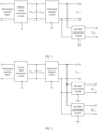
- FIG. 1 is a schematic diagram of an on-board charger.
- a power factor correction (Power Factor Correction, PFC) circuit 01 can convert an alternating current input into a direct current output, and output a direct current to an on-board charger (On Board Charger, OBC) circuit 02.
- the on-board charger circuit 02 is configured to charge a power battery pack of an electric vehicle. That is, a high-voltage side V HV is connected to the power battery pack in the figure. When the electric vehicle is in a driving mode, the alternating current input is disconnected.
- a DC-DC conversion circuit 03 is configured to convert a high voltage of the power battery pack into a low voltage, to supply electric energy to a low-voltage system of the electric vehicle.
- the low-voltage system of the electric vehicle may not operate normally, and safe operation of the electric vehicle is threatened.
- the electric vehicle is provided with a low-voltage battery as an alternative power supply when the DC-DC conversion circuit 03 is faulty.
- a capacity and a discharging capability of the low-voltage battery are limited, and the low-voltage system still cannot operate normally when the capacity is excessively low.
- two DC-DC conversion circuits are connected at a high-voltage side to implement dual redundant outputs. However, costs of implementing this solution are high.
- This application provides a charging circuit of an on-board charger, an on-board charger, and a charging control method, to provide dual redundant low-voltage direct current outputs.
- this application provides a charging circuit of an on-board charger.
- the charging circuit includes a first power conversion circuit and a second power conversion circuit.
- a second end of the first power conversion circuit is connected to a first end of the second power conversion circuit, a high-voltage output end of the second power conversion circuit charges a power battery pack of an electric vehicle, and a first low-voltage output end of the second power conversion circuit supplies power to a low-voltage system of the electric vehicle.
- the first power conversion circuit is configured to, when the electric vehicle is in a charging mode, convert an alternating current input from a first end of the first power conversion circuit into a direct current and transmit the direct current to the first end of the second power conversion circuit.
- the first power conversion circuit functions as a power factor correction circuit. That is, the first power conversion circuit has a function of the power factor correction circuit and implements alternating current-direct current conversion.
- the first power conversion circuit is further configured to, when the electric vehicle is in a driving mode, perform direct current conversion on the direct current obtained from the second power conversion circuit and supply a converted current to the low-voltage system. In this case, the first power conversion circuit functions as a DC-DC conversion circuit.
- the second power conversion circuit is configured to, when the electric vehicle is in the driving mode, convert a high voltage of the power battery pack into a low voltage, transmit the low voltage to the first low-voltage output end, and output a direct current to the first power conversion circuit.
- the first power conversion circuit of the charging circuit has different functions when the electric vehicle is in different modes. Specifically, the first power conversion circuit functions as the power factor correction circuit when the electric vehicle is in the charging mode, and functions as the DC-DC conversion circuit when the electric vehicle is in the driving mode. Therefore, dual redundant low-voltage direct current outputs can be provided, so that an additional DC-DC circuit is not needed. This reduces complexity of the solution and a space occupied by a circuit, and can further reduce costs and materials.
- the first power conversion circuit and the second power conversion circuit each include a controllable switching transistor.
- the charging circuit further includes a controller.
- the controller is configured to control operating states of the controllable switching transistors in the first power conversion circuit and the second power conversion circuit, so that the first power conversion circuit and the second power conversion circuit implement the foregoing functions when the electric vehicle is in the charging mode and the driving mode.
- the controller may adjust a pulse width modulation (Pulse Width Modulation, PWM) signal sent to each controllable switching transistor, to control an operating state of the switching transistor.
- PWM pulse width modulation
- the second power conversion circuit includes a primary-side switching circuit, a first transformer, a high-voltage secondary-side switching circuit, and a low-voltage secondary-side switching circuit.
- a first end of the primary-side switching circuit is the first end of the second power conversion circuit, and a second end of the primary-side switching circuit is connected to a primary-side winding of the first transformer.
- a high-voltage secondary-side winding of the first transformer is connected to a first end of the high-voltage secondary-side switching circuit, and a second end of the high-voltage secondary-side switching circuit is the high-voltage output end of the second power conversion circuit.
- a low-voltage secondary-side winding of the first transformer is connected to a first end of the low-voltage secondary-side switching circuit, and a second end of the low-voltage secondary-side switching circuit is the first low-voltage output end of the second power conversion circuit.
- the controller is configured to, when the electric vehicle is in the driving mode, control a switching transistor in the high-voltage secondary-side switching circuit, to convert a direct current input by the power battery pack into an alternating current and then transmit the alternating current to the high-voltage secondary-side winding.
- the controller is further configured to, when the electric vehicle is in the driving mode, control a switching transistor in the primary-side switching circuit, to convert an alternating current input by the primary-side winding into a direct current and transmit the direct current to the first power conversion circuit.
- the controller is further configured to, when the electric vehicle is in the driving mode, control a switching transistor in the low-voltage secondary-side switching circuit, to convert an alternating current transmitted by the low-voltage secondary-side winding into a direct current and transmit the direct current to the first low-voltage output end.
- the second power conversion circuit is configured to convert the high voltage of the power battery pack into a low voltage needed by the low-voltage system and output the low voltage, to form a first low-voltage direct current output.
- the first power conversion circuit specifically includes a full-bridge switching circuit, a second transformer, a first switching transistor, a second switching transistor, a first capacitor, and a first inductor
- the full-bridge switching circuit includes two bridge arms. An upper half bridge arm and a lower half bridge arm of each of the two bridge arms each include a switching transistor. An output end of the full-bridge switching circuit is the second end of the first power conversion circuit.
- a middle point of a first bridge arm is connected in series to a primary-side winding of the second transformer and then is connected to one port of the first end of the first power conversion circuit.
- a middle point of a second bridge arm is connected to the other port of the first end of the first power conversion circuit.
- a first end of a secondary-side winding of the second transformer is connected in series to the first switching transistor and then is connected to a first end point.
- a second end of the secondary-side winding of the second transformer is connected in series to the second switching transistor and then is connected to the first end point.
- a central tap of the secondary-side winding of the second transformer is sequentially connected in series to the first capacitor and the first inductor and then is connected to the first end point.
- the first end point is connected to one port of a second low-voltage output end, and the other port of the second low-voltage output end is connected between the first inductor and the first capacitor.
- the first power conversion circuit can implement a function of the power factor correction circuit and a function of the DC-DC conversion circuit. Therefore, function multiplexing is implemented, and an additional complete DC-DC circuit is not needed.
- the controller controls a switching transistor in the full-bridge switching circuit, the first switching transistor, and the second switching transistor, so that the first power conversion circuit performs direct current conversion on a direct current obtained from the primary-side switching circuit and transmits a converted current to the second low-voltage output end, to form a second low-voltage direct current output.
- the first power conversion circuit further includes a third switching transistor.
- the other port of the second low-voltage output end is connected between the first inductor and the first capacitor specifically includes: A first end of the third switching transistor is connected between the first inductor and the first capacitor, and a second end of the third switching transistor is connected to the other port of the second low-voltage output end.
- the controller controls the third switching transistor to be turned off, to prevent an induced voltage generated on the second transformer from being transmitted to the second low-voltage output end.
- the controller controls the third switching transistor to be turned on, so that the first power conversion circuit is connected to the second low-voltage output end. Therefore, the first power conversion circuit can supply power to the low-voltage system through the second low-voltage output end.
- the charging circuit further includes a first switch and a second switch.
- a first end of the first switch is connected to a first alternating current port, and a second end of the first switch is connected to a first end of the second switch.
- the middle point of the first bridge arm is connected in series to the primary-side winding of the second transformer and then is connected to a second end of the second switch.
- the second end of the second switch is connected to a second alternating current port, and the first end of the second switch is further connected to the middle point of the second bridge arm.
- the controller controls the first switch to be turned on and the second switch to be turned off, so that the first power conversion circuit is connected to an alternating current port.
- the controller controls the first switch to be turned off and the second switch to be turned on, so that the first power conversion circuit and the alternating current port are disconnected, and the middle point of the first bridge arm of the full-bridge switching circuit is sequentially connected to the primary-side winding of the second transformer and the middle point of the second bridge arm, to form a closed circuit.
- the first power conversion circuit can implement a DC-DC conversion function.
- the first power conversion circuit specifically includes a full-bridge switching circuit, a first inductor, a first switch, a second switch, and a first capacitor.
- the full-bridge switching circuit includes two bridge arms. An upper half bridge arm and a lower half bridge arm of each of the two bridge arms each include a switching transistor. A middle point of a first bridge arm is connected to a first end of the first switch, the middle point of the first bridge arm is further connected to one port of the first end of the first power conversion circuit, and a second end of the first switch is connected to one port of a second low-voltage output end.
- a middle point of a second bridge arm is connected in series to the first inductor and then is connected to a first end of the second switch and the other port of the first end of the first power conversion circuit.
- a second end of the second switch is connected to the other port of the second low-voltage output end.
- the first capacitor is connected in parallel between the second end of the first switch and the second end of the second switch.
- An output end of the full-bridge switching circuit is the second end of the first power conversion circuit.
- the first power conversion circuit can implement a function of the power factor correction circuit and a function of the DC-DC conversion circuit that is specifically a Buck (Buck) circuit. Therefore, function multiplexing is implemented, and an additional complete DC-DC circuit is not needed.
- the controller controls the first switch and the second switch to be turned on, and controls an operating state of a switching transistor in the full-bridge switching circuit, so that the first power conversion circuit performs direct current conversion on a direct current obtained from the primary-side switching circuit and transmits a converted current to the second low-voltage output end, to form a second low-voltage direct current output.
- the charging circuit further includes a third switch and a fourth switch.
- a first end of the third switch is connected to a first alternating current port, and a second end of the third switch is connected to a port of the first end of the first power conversion circuit.
- a first end of the fourth switch is connected to a second alternating current port, and a second end of the fourth switch is connected to the other port of the first end of the first power conversion circuit.
- the controller controls the third switch and the fourth switch to be turned on, so that the first power conversion circuit is connected to an alternating current port.
- the controller controls the third switch and the fourth switch to be turned off, so that the first power conversion circuit and the alternating current port are disconnected.
- a positive output end of the second low-voltage output end is connected to a positive output end of the first low-voltage output end, and a negative output end of the second low-voltage output end is connected to a negative output end of the first low-voltage output end.
- the charging circuit presents a low-voltage output end for an externally connected low-voltage system of the electric vehicle.
- the controller controls the switching transistor in the full-bridge switching circuit to convert an alternating current input from an input end of the full-bridge switching circuit into a direct current and supply the direct current to the primary-side switching circuit.
- the controller is further configured to, when the electric vehicle is in the charging mode, control a switching transistor in the primary-side switching circuit, so that the primary-side switching circuit converts the direct current into an alternating current, transmits the alternating current to a high-voltage output end through the first transformer to charge the power battery pack, and transmits the alternating current to a first low-voltage output end to supply power to the low-voltage system.
- the controller controls the switching transistor of the upper half bridge arm of the first bridge arm and the switching transistor of the lower half bridge arm of the second bridge arm to be simultaneously turned on or turned off, controls the switching transistor of the lower half bridge arm of the first bridge arm and the switching transistor of the upper half bridge arm of the second bridge arm to be simultaneously turned on or turned off, and controls the switching transistor of the upper half bridge arm of the first bridge arm and the switching transistor of the lower half bridge arm of the first bridge arm not to be simultaneously turned on, to convert the direct current obtained from the primary-side switching circuit into an alternating current and then transmit the alternating current to the primary -side winding of the second transformer. In this way, the secondary-side winding of the second transformer generates a corresponding induced voltage.
- an output voltage of the full-bridge switching circuit can also be controlled by adjusting a duty cycle of a control signal of each switching transistor.
- the controller controls the switching transistor of the upper half bridge arm of the first bridge arm to maintain a turn-on state, controls the switching transistor of the lower half bridge arm of the first bridge arm to maintain a turn-off state, and controls the switching transistor of the upper half bridge arm of the second bridge arm and the switching transistor of the lower half bridge arm of the second bridge arm to be alternately turned on.
- the first power conversion circuit is equivalent to a Buck circuit, reduces a voltage of the direct current obtained from the primary-side switching circuit, and then transmits a voltage-reduced current to the second low-voltage output end.
- the controller may adjust an output voltage by adjusting a duty cycle of a control signal of the switching transistor of the upper half bridge arm of the second bridge arm and a duty cycle of a control signal of the switching transistor of the lower half bridge arm of the second bridge arm.
- the controller is further configured to adjust a control signal of a switching transistor in the full-bridge switching circuit based on an output voltage of the second low-voltage output end and a preset voltage.
- a load of the low-voltage system may change. Therefore, to enable the low-voltage system to operate normally, a voltage output by the second low-voltage output end needs to be adjusted in real time to match the preset voltage, where the preset voltage represents a voltage required by the current low-voltage system.
- the controller when the output voltage of the second low-voltage output end is less than the preset voltage, the controller increases a duty cycle of the control signal of the switching transistor in the full-bridge switching circuit, so that the output voltage of the second low-voltage output end is increased to the preset voltage; and when the output voltage of the second low-voltage output end is greater than the preset voltage, the controller reduces the duty cycle of the control signal of the switching transistor in the full-bridge switching circuit, so that the output voltage of the second low-voltage output end is reduced to the preset voltage. Further, the output voltage of the second low-voltage output end can be adjusted according to a real-time requirement, thereby improving availability of the charging circuit.
- the controller is further configured to adjust a duty cycle of a control signal of a controllable switching transistor in the primary-side switching circuit and/or the high-voltage secondary-side switching circuit, so that a direct current voltage output by the primary-side switching circuit to the first power conversion circuit remains stable.
- the duty cycle of the control signal of the controllable switching transistor in the primary-side switching circuit and/or the high-voltage secondary-side switching circuit may be adjusted, for example, the duty cycle may be increased.
- control over a switching transistor in the second power conversion circuit is decoupled from control over a switching transistor in the full-bridge switching circuit, so that the switching transistor in the second power conversion circuit and the switching transistor in the full-bridge switching circuit can be separately controlled without affecting each other.
- control logic is simplified.
- the charging circuit further includes a secondary-side high-voltage capacitor and a secondary-side low-voltage capacitor.
- the secondary-side high-voltage capacitor is connected in parallel to a positive output end and a negative output end of the high-voltage output end.
- the secondary-side low-voltage capacitor is connected in parallel to a positive output end and a negative output end of the low-voltage output end.
- the charging circuit further includes a bus capacitor.
- the bus capacitor is connected in parallel between two ports at the second end of the first power conversion circuit.
- the bus capacitor is configured to reduce fluctuation of a direct current voltage.
- the controllable switching transistors in the first power conversion circuit and the second power conversion circuit are controlled by a same controller or a plurality of controllers.
- the switching transistors of the first power conversion circuit are controlled by one controller, and the switching transistors of the second power conversion circuit are controlled by another controller.
- switching transistors connected to a high-voltage output end are controlled by one controller, to be specific, the switching transistors in the full-bridge switching circuit, the primary-side switching circuit, and the high-voltage secondary-side switching circuit are controlled by one controller; and switching transistors connected to a low-voltage output end are controlled by another controller.
- this application further provides an on-board charger.
- the on-board charger includes the charging circuit of an on-board charger provided in any one of the foregoing possible implementations, and further includes an electromagnetic interference EMI filter circuit.
- An input end of the electromagnetic interference filter circuit is connected to an alternating current input of the on-board charger, and an output end is connected to the first end of the first power conversion circuit.
- the electromagnetic interference filter circuit is configured to filter out electromagnetic interference.
- this application further provides a charging control method.
- the method is applied to a charging circuit of an on-board charger and includes:
- the first power conversion circuit may have different functions when the electric vehicle is in different modes. Specifically, the first power conversion circuit functions as a power factor correction circuit when the electric vehicle is in the charging mode, and functions as a DC-DC conversion circuit when the electric vehicle is in the driving mode. Therefore, dual redundant low-voltage direct current outputs are provided, so that an additional DC-DC circuit is not needed, and costs are reduced.
- the second power conversion circuit includes a primary-side switching circuit, a first transformer, a high-voltage secondary-side switching circuit, and a low-voltage secondary-side switching circuit.
- a first end of the primary-side switching circuit is the first end of the second power conversion circuit, and a second end of the primary-side switching circuit is connected to a primary-side winding of the first transformer.
- a high-voltage secondary-side winding of the first transformer is connected to a first end of the high-voltage secondary-side switching circuit, and a second end of the high-voltage secondary-side switching circuit is a high-voltage output end of the second power conversion circuit.
- a low-voltage secondary-side winding of the first transformer is connected to a first end of the low-voltage secondary-side switching circuit, and a second end of the low-voltage secondary-side switching circuit is the first low-voltage output end of the second power conversion circuit.
- the controlling, when the electric vehicle is in a driving mode, the second power conversion circuit to convert a high voltage of a power battery pack into a low voltage, transmit the low voltage to a first low-voltage output end, and output a direct current to the first power conversion circuit specifically includes:
- the first power conversion circuit specifically includes a full-bridge switching circuit, a second transformer, a first switching transistor, a second switching transistor, a first capacitor, and a first inductor
- the full-bridge switching circuit includes two bridge arms. An upper half bridge arm and a lower half bridge arm of each of the two bridge arms each include a switching transistor.
- An output end of the full-bridge switching circuit is a second end of the first power conversion circuit, and another output end of the full-bridge switching circuit is a first end of the first power conversion circuit.
- a middle point of a first bridge arm is connected in series to a primary-side winding of the second transformer and then is connected to one port of the first end of the first power conversion circuit.
- a middle point of a second bridge arm is connected to the other port of the first end of the first power conversion circuit.
- a first end of a secondary-side winding of the second transformer is connected in series to the first switching transistor and then is connected to a first end point.
- a second end of the secondary-side winding of the second transformer is connected in series to the second switching transistor and then is connected to the first end point.
- a central tap of the secondary-side winding of the second transformer is sequentially connected in series to the first capacitor and the first inductor and then is connected to the first end point.
- the first end point is connected to a negative output end of a second low-voltage output end, and a positive output end of the second low-voltage output end is connected between the first inductor and the first capacitor.
- the first power conversion circuit further includes a third switching transistor. That the positive output end of the second low-voltage output end is connected between the first inductor and the first capacitor specifically includes: A first end of the third switching transistor is connected between the first inductor and the first capacitor, and a second end of the third switching transistor is connected to the positive output end of the second low-voltage output end.
- the method further includes: controlling, when the electric vehicle is in the charging mode, the third switching transistor to be turned off; and controlling, when the electric vehicle is in the driving mode, the third switching transistor to be turned on.
- the charging circuit further includes a first switch and a second switch.
- a first end of the first switch is connected to a first alternating current port, and a second end of the first switch is connected to a first end of the second switch.
- the middle point of the first bridge arm is connected in series to the primary-side winding of the second transformer and then is connected to a second end of the second switch.
- the second end of the second switch is connected to a second alternating current port, and the first end of the second switch is further connected to the middle point of the second bridge arm.
- the method further includes: controlling, when the electric vehicle is in the charging mode, the first switch to be turned on and the second switch to be turned off; and controlling, when the electric vehicle is in the driving mode, the first switch to be turned off and the second switch to be turned on.
- the first power conversion circuit specifically includes a full-bridge switching circuit, a first inductor, a first switch, a second switch, and a first capacitor.
- the full-bridge switching circuit includes two bridge arms. An upper half bridge arm and a lower half bridge arm of each of the two bridge arms each include a switching transistor. A middle point of a first bridge arm is connected to a first end of the first switch, the middle point of the first bridge arm is further connected to one port of the first end of the first power conversion circuit, and a second end of the first switch is connected to a positive output end of the second low-voltage output end.
- a middle point of a second bridge arm is connected in series to the first inductor and then is connected to a first end of the second switch and the other port of the first end of the first power conversion circuit.
- a second end of the second switch is connected to a negative output end of the second low-voltage output end.
- the first capacitor is connected in parallel between the second end of the first switch and the second end of the second switch.
- An output end of the full-bridge switching circuit is the second end of the first power conversion circuit.
- the method further includes: when the electric vehicle is in the driving mode, controlling the first switch and the second switch to be turned on, and controlling an operating state of a switching transistor in the full-bridge switching circuit, so that the first power conversion circuit performs direct current conversion on a direct current obtained from the primary-side switching circuit and then transmits a converted current to the second low-voltage output end.
- the charging circuit further include a third switch and a fourth switch.
- a first end of the third switch is connected to a first alternating current port, and a second end of the third switch is connected to a port of the first end of the first power conversion circuit.
- a first end of the fourth switch is connected to a second alternating current port, and a second end of the fourth switch is connected to the other port of the first end of the first power conversion circuit.
- the method further includes:
- the positive output end of the second low-voltage output end is connected to a positive output end of the first low-voltage output end
- the negative output end of the second low-voltage output end is connected to a negative output end of the first low-voltage output end
- the controlling an operating state of a switching transistor in the full-bridge switching circuit specifically includes: controlling the switching transistor of the upper half bridge arm of the first bridge arm and the switching transistor of the lower half bridge arm of the second bridge arm to be simultaneously turned on or turned off, controlling the switching transistor of the lower half bridge arm of the first bridge arm and the switching transistor of the upper half bridge arm of the second bridge arm to be simultaneously turned on or turned off, and controlling the switching transistor of the upper half bridge arm of the first bridge arm and the switching transistor of the lower half bridge arm of the first bridge arm not to be simultaneously turned on.
- the controlling an operating state of a switching transistor in the full-bridge switching circuit specifically includes: controlling the switching transistor of the upper half bridge arm of the first bridge arm to maintain a turn-on state, controlling the switching transistor of the lower half bridge arm of the first bridge arm to maintain a turn-off state, and controlling the switching transistor of the upper half bridge arm of the second bridge arm and the switching transistor of the lower half bridge arm of the second bridge arm to be alternately turned on.
- the first power conversion circuit is equivalent to a Buck circuit, and performs voltage reduction on a direct current obtained from the primary-side switching circuit, and then transmits a voltage-reduced current to the second low-voltage output end.
- An output voltage is adjusted by adjusting a duty cycle of a control signal of the switching transistor of the upper half bridge arm of the second bridge arm and a duty cycle of a control signal of the switching transistor of the lower half bridge arm of the second bridge arm.
- the method further includes: adjusting a control signal of a switching transistor in the full-bridge switching circuit based on an output voltage of the second low-voltage output end and a preset voltage.
- a load of the low-voltage system may change. Therefore, to enable the low-voltage system to operate normally, a voltage output by the second low-voltage output end needs to be adjusted in real time to match the preset voltage, where the preset voltage represents a voltage required by the current low-voltage system.
- the adjusting a control signal of a switching transistor in the full-bridge switching circuit based on an output voltage of the second low-voltage output end and a preset voltage specifically includes: increasing a duty cycle of the control signal of the switching transistor in the full-bridge switching circuit when the output voltage of the second low-voltage output end is less than the preset voltage, so that the output voltage of the second low-voltage output end is increased to the preset voltage; and reducing the duty cycle of the control signal of the switching transistor in the full-bridge switching circuit when the output voltage of the second low-voltage output end is greater than the preset voltage, so that the output voltage of the second low-voltage output end is reduced to the preset voltage.
- the output voltage of the second low-voltage output end can be adjusted according to a real-time requirement, thereby improving availability of the charging circuit.
- the method further includes: adjusting a duty cycle of a control signal of a controllable switching transistor in the primary-side switching circuit and/or the high-voltage secondary-side switching circuit, so that a direct current voltage output by the primary-side switching circuit to the first power conversion circuit remains stable.
- control over a switching transistor in the second power conversion circuit is decoupled from control over a switching transistor in the full-bridge switching circuit, so that the switching transistor in the second power conversion circuit and the switching transistor in the full-bridge switching circuit can be separately controlled without affecting each other.
- control logic is simplified.
- the charging circuit includes the first power conversion circuit and the second power conversion circuit.
- the first power conversion circuit can convert an alternating current input from an input end into a direct current and supply the direct current to the second power conversion circuit.
- the first power conversion circuit functions as a power factor correction circuit. That is, the first power conversion circuit has a function of the power factor correction circuit and implements alternating current-direct current conversion.
- the high-voltage output end of the second power conversion circuit charges the power battery pack of the electric vehicle, and the first low-voltage output end of the second power conversion circuit supplies power to the low-voltage system of the electric vehicle.
- a high-voltage direct current provided by the power battery pack can be converted into a low-voltage direct current through the second power conversion circuit, and then the low-voltage direct current is supplied to the low-voltage system through the first low-voltage output end, to form a first low-voltage direct current output.
- the second power conversion circuit can also convert a high voltage obtained from the power battery pack into a direct current through current conversion and transmit the direct current to the first power conversion circuit, and the first power conversion circuit performs direct current conversion on the obtained direct current and then supplies the direct current to the low-voltage system, to form a second low-voltage direct current output.
- the first power conversion circuit functions as a DC-DC conversion circuit.
- the charging circuit can provide dual redundant low-voltage direct current outputs when the electric vehicle is in the driving mode, so that reliability of supplying power to the low-voltage system by the electric vehicle is improved.
- the first power conversion circuit has different functions when the electric vehicle is in different modes. Specifically, the first power conversion circuit functions as a power factor correction circuit when the electric vehicle is in the charging mode, and functions as a DC-DC conversion circuit when the electric vehicle is in the driving mode, so that an additional DC-DC circuit is not needed. Therefore, costs are reduced.
- a low-voltage battery is used as a substitute power supply when a DC-DC conversion circuit fails.
- a capacity and a discharge capability of the low-voltage battery are limited, when a battery level of the low-voltage battery is excessively low, the low-voltage system still cannot operate normally.
- two groups of DC-DC conversion circuits may be connected at a high-voltage side, to implement dual redundant low-voltage direct current outputs. This is described below with reference to an accompanying drawing.
- FIG. 2 is a schematic diagram of another on-board charger according to an embodiment of this application.
- a high-voltage side V HV of the on-board charger is connected to two DC-DC conversion circuits, namely, a DC-DC conversion circuit 03a and a DC-DC conversion circuit 03b, to implement dual redundant low-voltage direct current outputs.
- a DC-DC converter circuit is additionally added, implementation costs of this solution are high.
- embodiments of this application provide a charging circuit of an on-board charger, an on-board charger, and a charging control method.
- energy of a power battery pack is transmitted to a direct current busbar side by a second power conversion circuit.
- One part of the energy is converted into a low voltage by the second power conversion circuit, and the other part is converted into a low voltage by a first power conversion circuit operating in a DC-DC conversion mode, to provide two redundant low-voltage direct current outputs.
- the first power conversion circuit functions as a power factor correction circuit when the charging circuit charges the power battery pack, that is, when an electric vehicle is in a charging mode, and functions as a DC-DC conversion circuit when the electric vehicle is in the driving mode, so that an additional DC-DC conversion circuit is not needed. Therefore, costs are reduced.
- first”, “second”, and the like are merely intended for a purpose of description, and shall not be understood as an indication or implication of relative importance or implicit indication of a quantity of indicated technical features. Therefore, a feature limited by “first”, “second”, or the like may explicitly or implicitly include one or more features.
- orientation terms such as “left” and “right” may include but are not limited to being defined relative to orientations of components shown in the accompanying drawings. It should be understood that these orientation terms may be relative concepts, are used for description and clarification of the components, and may be correspondingly changed based on changes of the orientations of components shown in the accompanying drawings.
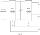
- FIG. 3 is a schematic diagram of a charging circuit of an on-board charger according to an embodiment of this application.
- the charging circuit of an on-board charger includes a first power conversion circuit 101 and a second power conversion circuit 102.
- the charging circuit of an on-board charger provided in this embodiment of this application can operate in the following two operating modes: a charging mode and a driving mode.
- an electric vehicle is connected to an alternating current power supply, and a power battery pack is charged by using an on-board charger.
- a first end of the first power conversion circuit 101 is connected to the alternating current power supply.
- the electric vehicle does not use an alternating current power supply to charge the power battery pack.
- the driving mode in this embodiment of this application does not only mean that the electric vehicle is in a driving state, but means that the electric vehicle is in a state in which the power battery pack is not currently charged, that is, the driving mode is a non-charging mode. In the driving mode, no alternating current is input to the first end of the first power conversion circuit 101.
- a second end of the first power conversion circuit 101 is connected to a first end of the second power conversion circuit 102, and output ends of the second power conversion circuit 102 include a high-voltage output end (represented by HV in the figure) and a first low-voltage output end (represented by LV1 in the figure).
- the high-voltage output end HV charges the power battery pack of the electric vehicle, and the first low-voltage output end LV1 supplies power to a low-voltage system of the electric vehicle.
- the first power conversion circuit 101 converts the alternating current input from the first end into a direct current and supplies the direct current to the second power conversion circuit. That is, the first power conversion circuit has a function of a power factor correction circuit and implements alternating current-direct current conversion.
- the second power conversion circuit 102 converts the direct current transmitted by the first power conversion circuit 101 into a high-voltage direct current to charge the power battery pack of the electric vehicle through the high-voltage output end HV, and converts the direct current transmitted by the first power conversion circuit 101 into a low-voltage direct current to supply power to the low-voltage system of the electric vehicle.
- the low-voltage system of the electric vehicle is powered by the power battery pack.
- the high-voltage direct current provided by the power battery pack can be converted into a low-voltage direct current by the second power conversion circuit 102, and then the low-voltage direct current is supplied to the low-voltage system through the first low-voltage output end LV1, to form a first low-voltage direct current output.
- the second power conversion circuit 102 can also convert a high voltage obtained from the power battery pack into a direct current through current conversion and transmit the direct current to the first power conversion circuit 101, and the first power conversion circuit 101 performs direct current conversion on the obtained direct current and then supplies the direct current to the low-voltage system, to form a second low-voltage direct current output.
- the first power conversion circuit 101 functions as a DC-DC conversion circuit.
- the first power conversion circuit of the charging circuit functions as a power factor correction circuit when the electric vehicle is in the charging mode, and functions as a DC-DC conversion circuit when the electric vehicle is in the driving mode. Therefore, the first power conversion circuit has different functions when the electric vehicle is in different modes.
- an output when the first power conversion circuit is used as a DC-DC conversion circuit is used as the second low-voltage direct current output, so that an additional DC-DC circuit is not needed. Therefore, dual redundant low-voltage direct current outputs are provided, and costs are reduced.
- the first power conversion circuit and the second power conversion circuit each include a switching transistor
- the charging circuit of an on-board charger further includes a controller (not shown in the figure).
- the controller implements the dual redundant low-voltage direct current outputs for the low-voltage system by controlling operating states of the switching transistors in the first power conversion circuit and the second power conversion circuit.
- the controller may be an application-specific integrated circuit (Application-specific Integrated Circuit, ASIC), a programmable logic device (Programmable Logic Device, PLD), a digital signal processor (Digital Signal Processor, DSP), or a combination thereof.
- the PLD may be a complex programmable logic device (Complex Programmable Logic Device, CPLD), a field-programmable gate array (Field-programmable Gate Array, FPGA), general array logic (Generic Array Logic, GAL), or any combination thereof. This is not specifically limited in this embodiment of this application.
- the controller is a controller of an on-board charger, and there may be one or more controllers. This is not specifically limited in this embodiment of this application. In other words, controllable switching transistors in the first power conversion circuit and the second power conversion circuit are controlled by a same controller or by a plurality of controllers.
- the switching transistor may be any of the following: a relay, an insulated gate bipolar transistor (Insulated Gate Bipolar Transistor, IGBT), a metal-oxide semiconductor field-effect transistor (Metal Oxide Semiconductor Field Effect Transistor, MOSFET, hereinafter referred to as a MOS transistor), a silicon carbide metal oxide semiconductor field-effect transistor (Silicon Carbide Metal Oxide Semiconductor, SiC MOSFET), or the like.
- the switching transistor is a MOS transistor
- the switching transistor may be specifically a PMOS transistor or an NMOS transistor. This is not specifically limited in this embodiment of this application. In the following descriptions, that the switching transistor is an NMOS transistor is used as an example.
- the switching transistor When the switching transistor is a device of another type, an operating principle is similar. Details are not described again in this embodiment of this application.
- the switching transistor is an NMOS transistor
- the NMOS transistor has a body diode. A cathode of the body diode is connected to a drain of the NMOS transistor, and an anode of the body diode is connected to a source of the NMOS transistor.
- the controller controls an operating state of the switching transistor by sending a pulse width modulation (Pulse Width Modulation, PWM) signal to the switching transistor.
- PWM Pulse Width Modulation
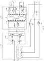
- FIG. 4 is a schematic diagram of another charging circuit of an on-board charger provided in this embodiment of this application.
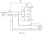
- a first power conversion circuit 101 of the charging circuit includes a full-bridge switching circuit 101a, a second transformer T2, a first switching transistor Q5, a second switching transistor Q6, a first capacitor C1, and a first inductor L1.
- a second power conversion circuit 102 of the charging circuit includes a primary-side switching circuit 102a, a first transformer T1, a high-voltage secondary-side switching circuit 102b, and a low-voltage secondary-side switching circuit 102c.
- the full-bridge switching circuit 101a includes two bridge arms, namely, a first bridge arm and a second bridge arm.
- An upper half bridge arm and a lower half bridge arm of each of the two bridge arms each include a switching transistor.
- the switching transistors of the full-bridge switching circuit are represented by Q1-Q4 in the figure.
- An output end of the full-bridge switching circuit 101a is a first end of the first power conversion circuit 101.
- a middle point of the first bridge arm is connected in series to a primary-side winding of the second transformer T2 and then is connected to one port of the first end of the first power conversion circuit 101. In the figure, this port is represented by B.
- a middle point of the second bridge arm is connected to the other port of the first end of the first power conversion circuit 101. In the figure, this port is represented by C.
- a first end of a secondary-side winding of the second transformer T2 is connected in series to the first switching transistor Q5 and then is connected to a first end point A.
- a second end of the secondary-side winding of the second transformer T2 is connected in series to the second switching transistor Q6 and then is connected to the first end point A.
- a central tap of the secondary-side winding of the second transformer T2 is sequentially connected in series to the first capacitor L1 and the first inductor C1 and then is connected to the first end point A.
- the first end point A is connected to one port of a second low-voltage output end, for example, to a negative output end in the figure.
- the other port of the second low-voltage output end for example, a positive output end in the figure, is connected between the first inductor L1 and the first capacitor C1.
- a first end of the primary-side switching circuit 102a is a first end of the second power conversion circuit 102, and a second end of the primary-side switching circuit 102a is connected to a primary-side winding L T1 of the first transformer T1.
- a high-voltage secondary-side winding L T2 of the first transformer T1 is connected to a first end of the high-voltage secondary-side switching circuit 102b, and a second end of the high-voltage secondary-side switching circuit 102b is a high-voltage output end of the second power conversion circuit 102.
- a low-voltage secondary-side winding L T3 of the first transformer T1 is connected to a first end of the low-voltage secondary-side switching circuit 102c, and a second end of the low-voltage secondary-side switching circuit 102c is a first low-voltage output end of the second power conversion circuit 102.
- two ports B and C of the first end of the first power conversion circuit 101 are connected to an alternating current input, and the alternating current input is provided by an external device.
- the external device may be a charging pile.
- a controller controls the first switch Q5 and the second switch Q6 to remain in a turn-off state.
- the alternating current passes through a primary-side winding L T4 of the second transformer T2 and the full-bridge switching circuit 101a, the alternating current is converted into a direct current, and the direct current is transmitted to the first end of the primary-side switching circuit 102a.
- the direct current passes through the primary-side switching circuit 102a, the primary-side winding L T1 , the high-voltage secondary-side winding L T2 , and the high-voltage secondary-side switching circuit 102b, energy is transmitted to the high-voltage output end to charge a power battery pack of the electric vehicle.
- the primary-side switching circuit 102a, the high-voltage secondary-side switching circuit 102b, and the low-voltage secondary-side switching circuit 102c each include a switching transistor.
- the controller can convert a direct current input from the first end of the primary-side switching circuit 102a into an alternating current by controlling an operating state of the switching transistor, and then use the transformer T 1 to enable a high-voltage alternating current to be input from the first end of the high-voltage secondary-side switching circuit 102b.
- the controller controls an operating state of the switching transistor in the high-voltage secondary-side switching circuit 102b, so that the high-voltage secondary-side switching circuit 102b rectifies the high-voltage alternating current into a high-voltage direct current and outputs the high-voltage direct current to the high-voltage output end.
- the controller further controls an operating state of the switching transistor in the low-voltage secondary-side switching circuit 102c, so that the low-voltage secondary-side switching circuit 102c rectifies a low-voltage alternating current into a low-voltage direct current and outputs the low-voltage direct current to the first low-voltage output end.
- the first power conversion circuit 101 functions as a PFC circuit and can implement alternating current-direct current conversion.
- the port B and the port C of the first end of the first power conversion circuit 101 are connected to form a circuit.
- the controller controls the switching transistor in the high-voltage secondary-side switching circuit 102b, to convert a high-voltage direct current output by the power battery pack into a high-voltage alternating current and then transmit the high-voltage alternating current to the first transformer T1.
- a low-voltage alternating current is input from the first end of the low-voltage secondary-side switching circuit 102c, and the controller controls the switching transistor in the low-voltage secondary-side switching circuit 102c, so that the low-voltage secondary-side switching circuit 102c rectifies the low-voltage alternating current into a low-voltage direct current and then outputs the low-voltage direct current, to form a first low-voltage direct current output.
- the second end of the primary -side switching circuit 102a obtains an alternating current from the first transformer T1.
- the controller rectifies the alternating current into a direct current by controlling the switching transistor of the primary-side switching circuit 102a and then transmits the direct current to a second end of the first power conversion circuit 101.
- the first power conversion circuit 101 performs DC-DC conversion on the direct current and outputs a converted current to the second low-voltage output end, to form a second low-voltage direct current output.
- transformer shown in FIG. 5 is first used as an example for descriptions.
- FIG. 7 is a schematic diagram 1 of an operating principle of the first power conversion circuit when the second transformer shown in FIG. 5 is used.
- the controller controls the switching transistors Q1 and Q4 in the full-bridge switching circuit 101a to be turned on, and the switching transistors Q2 and Q3 in the full-bridge switching circuit 101a to be turned off.
- a direction of a current of the primary-side winding L T4 of the second transformer T2 is from left to right shown in the figure, and a direction of an induced current of the secondary-side windings L T5 and L T6 of the second transformer T2 is from left to right shown in the figure.
- the controller controls the first switching transistor Q5 to be turned off and the second switching transistor Q6 to be turned on, so that a current output by the secondary-side winding L T5 passes through a filter circuit formed by the first inductor L1 and the first capacitor C1 and then is transmitted to the second low-voltage output end, to form the second low-voltage direct current output.
- FIG. 8 is a schematic diagram 2 of the operating principle of the first power conversion circuit when the second transformer shown in FIG. 5 is used.
- the controller controls the switching transistors Q2 and Q3 in the full-bridge switching circuit 101a to be turned on, and the switching transistors Q1 and Q4 in the full-bridge switching circuit 101a to be turned off.
- a direction of a current of the primary-side winding L T4 of the second transformer T2 is from right to left shown in the figure, and a direction of an induced current of the secondary-side windings L T5 and L T6 of the second transformer T2 is from right to left shown in the figure.
- the controller controls the first switching transistor Q5 to be turned on and the second switching transistor Q6 to be turned off, so that a current output by the secondary-side winding L T6 passes through the filter circuit formed by the first inductor L 1 and the first capacitor C1 and then is transmitted to the second low-voltage output end, to form the second low-voltage direct current output.
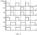
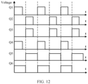
- FIG. 9 is a sequence diagram 1 of control signals of the controller provided in this embodiment of this application.
- the controller controls the switching transistor Q1 of the upper half bridge arm of the first bridge arm and the switching transistor Q4 of the lower half bridge arm of the second bridge arm to be simultaneously turned on or turned off, controls the switching transistor Q2 of the lower half bridge arm of the first bridge arm and the switching transistor Q3 of the upper half bridge arm of the second bridge arm to be simultaneously turned on or turned off, and controls the switching transistor Q1 of the upper half bridge arm of the first bridge arm and the switching transistor Q2 of the lower half bridge arm of the first bridge arm not to be simultaneously turned on.
- a duty cycle of a control signal of each of Q1 to Q4 is not specifically limited in this embodiment of this application.
- the controller can control complementary conduction between the first switching transistor Q5 and the second switching transistor Q6.
- the controller can adjust an output voltage of the second low-voltage output end by adjusting a duty cycle of a control signal (PWM signal) of a switching transistor in the full-bridge switching circuit 101a.
- the controller can adjust a control signal of a switching transistor in the full-bridge switching circuit based on the output voltage of the second low-voltage output end and a preset voltage.
- the preset voltage may be determined by the low-voltage system of the electric vehicle. This is not specifically limited in this embodiment of this application.
- the controller increases a duty cycle of a control signal of each of switching transistors in the full-bridge switching circuit, namely, a duty cycle of a control signal of each of the switching transistors Q 1 and Q2, so that the output voltage of the second low-voltage output end is increased to the preset voltage; and when the output voltage of the second low-voltage output end is greater than the preset voltage, the controller reduces the duty cycle of the control signal of each switching transistor in the full-bridge switching circuit, namely, the duty cycle of the control signal of each of the switching transistors Q1 and Q2, so that the output voltage of the second low-voltage output end is reduced to the preset voltage.
- the controller may adjust a duty cycle of a control signal of a controllable switching transistor in the primary-side switching circuit 102a and/or the high-voltage secondary-side switching circuit 102b, so that a direct current voltage output by the primary-side switching circuit 102a to the first power conversion circuit 101 remains stable.
- the direct current voltage obtained by the full-bridge switching circuit 101a from the first power conversion circuit 101 is relatively stable, and the output voltage of the second low-voltage output end can be adjusted only by adjusting a duty cycle of a drive signal of the controllable switching transistor in the first power conversion circuit 101.
- the output voltage of the second low-voltage output end may be detected in real time by a voltage sensor and a detection result is transmitted to the controller.
- the second transformer shown in FIG. 5 is used as an example for description.
- the second transformer shown in FIG. 6 is used as an example for description.
- FIG. 10 is a schematic diagram 1 of an operating principle of the first power conversion circuit when the second transformer shown in FIG. 6 is used.
- the controller controls the switching transistors Q1 and Q4 in the full-bridge switching circuit 101a to be turned on, and the switching transistors Q2 and Q3 in the full-bridge switching circuit 101a to be turned off.
- a direction of a current of the primary-side winding L T4 of the second transformer T2 is from left to right shown in the figure, and a direction of an induced current of the secondary-side windings L T5 and L T6 of the second transformer T2 is from right to left shown in the figure.
- the controller controls the first switching transistor Q5 to be turned on and the second switching transistor Q6 to be turned off, so that a current output by the secondary-side winding L T6 passes through the filter circuit formed by the first inductor L1 and the first capacitor C1 and then is transmitted to the second low-voltage output end, to form the second low-voltage direct current output.
- FIG. 11 is a schematic diagram 2 of the operating principle of the first power conversion circuit when the second transformer shown in FIG. 6 is used.
- the controller controls the switching transistors Q2 and Q3 in the full-bridge switching circuit 101a to be turned on, and the switching transistors Q1 and Q4 in the full-bridge switching circuit 101a to be turned off.
- a direction of a current of the primary-side winding L T4 of the second transformer T2 is from right to left shown in the figure, and a direction of an induced current of the secondary-side windings L T5 and L T6 of the second transformer T2 is from right to left shown in the figure.
- the controller controls the first switching transistor Q5 to be turned off and the second switching transistor Q6 to be turned on, so that a current output by the secondary-side winding L T5 passes through the filter circuit formed by the first inductor L1 and the first capacitor C1 and then is transmitted to the second low-voltage output end, to form the second low-voltage direct current output.
- FIG. 12 is a sequence diagram 2 of control signals of the controller provided in this embodiment of this application.
- a difference between FIG. 12 and FIG. 9 lies in that waveforms of control signals of the first switching transistor Q5 and the second switching transistor Q6 sent by the controller are opposite.
- the charging circuit further includes a secondary-side high-voltage capacitor C HV1 and a secondary-side low-voltage capacitor C LV1 .
- the secondary-side high-voltage capacitor C HV1 is connected in parallel between a positive output end and a negative output end of the high-voltage output end, to reduce voltage fluctuation of the high-voltage output end.
- the secondary-side low-voltage capacitor C LV1 is connected in parallel between a positive output end and a negative output end of the low-voltage output end, to reduce voltage fluctuation of the low-voltage output end.
- the charging circuit further includes a bus capacitor C Bus .
- the bus capacitor C Bus is connected in parallel between two ports of the second end of the first power conversion circuit 101, and is configured to reduce fluctuation of a direct current voltage transmitted between the first power conversion circuit 101 and the second power conversion circuit 102.
- FIG. 13 is a schematic diagram of still another charging circuit of an on-board charger provided in this embodiment of this application.
- a first end of the third switching transistor Q7 is connected between the first inductor L1 and the first capacitor C1, and a second end of the third switching transistor Q7 is connected to a positive output end of the second low-voltage output end.
- the controller controls the third switching transistor Q3 to be turned off, so that the second low-voltage output end has no output; and when the electric vehicle is in the driving mode, the controller controls the third switching transistor Q3 to be turned on.
- the third switching transistor Q3 may not be disposed. In this case, when the electric vehicle is in the charging mode, the controller controls the first switching transistor Q5 and the second switching transistor Q6 to be turned off, so that the second low-voltage output end has no output.
- a first end of the first switch S1 is connected to a first alternating current port, and a second end of the first switch S1 is connected to a first end of the second switch S2.
- the second end of the first switch S1 is represented by C.
- the middle point of the first bridge arm of the full-bridge switching circuit 101a is connected in series to the primary-side winding L T4 of the second transformer and then is connected to a second end of the second switch S2.
- the second end of the second switch S2 is represented by B.
- the second end of the second switch S2 is connected to a second alternating current port.
- the first end of the second switch S2 is also connected to the middle point of the second bridge arm of the full-bridge switching circuit 101a
- the controller controls the first switch S1 to be turned on and the second switch S2 to be turned off, so that the two ports of the first end of the first power conversion circuit 101 are respectively connected to the two alternating current ports. In this way, an alternating current is input to the first power conversion circuit 101.
- the controller controls the first switch S1 to be turned off and the second switch S2 to be turned on.
- the first end of the first power conversion circuit 101 is disconnected from an alternating current port, and the middle point of the first bridge arm of the full-bridge switching circuit 101a is connected in series to the primary-side winding L T4 of the second transformer and then is connected to the middle point of the second bridge arm, to form a circuit.
- the first switch S1 and the second switch S2 may be relays, or other controllable switches that can be used in an alternating current circuit. This is not specifically limited in this embodiment of this application.
- each low-voltage direct current output corresponds to one low-voltage output end is used as an example for description.
- the charging circuit includes the following two low-voltage output ends: a first low-voltage output end and a second low-voltage output end.
- the first low-voltage output end and the second low-voltage output end may be connected in parallel.
- the charging circuit presents a low-voltage output end for an externally connected low-voltage system of the electric vehicle. This is described in detail below with reference to an accompanying drawing.
- FIG. 14 is a schematic diagram of yet another charging circuit of an on-board charger provided in this embodiment of this application.
- the positive output end of the second low-voltage output end is connected to a positive output end of the first low-voltage output end, and a negative output end of the second low-voltage output end is connected to a negative output end of the first low-voltage output end.
- the two low-voltage direct current outputs are connected in parallel, to jointly supply power to the low-voltage system of the electric vehicle.
- controllers there may be one or more controllers in this embodiment of this application.
- the switching transistors of the first power conversion circuit are controlled by one controller, and the switching transistors of the second power conversion circuit are controlled by another controller.
- switching transistors connected to a high voltage are controlled by one controller, that is, the switching transistors in the full-bridge switching circuit 101a, the primary-side switching circuit 102a, and the high-voltage secondary-side switching circuit 102b are controlled by one controller; and switching transistors connected to a low voltage is controlled by another controller, that is, the low-voltage secondary-side switching circuit, the first switching transistor Q5, and the second switching transistor Q6 are controlled by another controller.
- the first power conversion circuit of the charging circuit provided in this embodiment of this application functions as a power factor correction circuit when the electric vehicle is in the charging mode, and functions as a DC-DC conversion circuit when the electric vehicle is in the driving mode. Therefore, the first power conversion circuit has different functions when the electric vehicle is in different modes. An output when the first power conversion circuit is used as a DC-DC conversion circuit is used as the second low-voltage direct current output, so that an additional DC-DC circuit is not needed. Therefore, the charging circuit provided in this embodiment of this application provides dual redundant low-voltage direct current outputs, and costs are reduced.
- FIG. 15 is a schematic diagram of another charging circuit of an on-board charger provided in this embodiment of this application.
- a first power conversion circuit 101 of the charging circuit includes a full-bridge switching circuit 101a, a first inductor L1, a first switch S1, a second switch S2, and a first capacitor C1.
- a second power conversion circuit 102 of the charging circuit includes a primary-side switching circuit 102a, a first transformer T1, a high-voltage secondary-side switching circuit 102b, and a low-voltage secondary-side switching circuit 102c.
- the second power conversion circuit 102 has the same structure and operating principle as the second power conversion circuit in the charging circuit embodiment 2. Details are not described herein again in this embodiment of this application.
- An output end of the full-bridge switching circuit 101a is a second end of the first power conversion circuit 101.
- the full-bridge switching circuit 101a includes two bridge arms. An upper half bridge arm and a lower half bridge arm of each of the two bridge arms each include a switching transistor. A middle point of a first bridge arm is connected to a first end of the first switch S1, and the middle point of the first bridge arm is also connected to a port of a first end of the first power conversion circuit 101, where the port is represented by a port C in the figure. A middle point of the second bridge arm is connected in series to the first inductor L1 and then connected to the other port of the first end of the first power conversion circuit 101, where the other port is represented by a port B in the figure.
- the middle point of the second bridge arm is connected in series to the first inductor L1 and then is connected to a first end of the second switch S2, and a second end of the second switch S2 is connected to a port of a second low-voltage output end, for example, to a negative output end as shown in the figure.
- a second end of the first switch S1 is connected to the other port of the second low-voltage output end, for example, to a positive output end as shown in the figure.
- the first capacitor C1 is connected in parallel between the second end of the first switch S1 and the second end of the second switch S2.
- the first capacitor C1 is configured to reduce fluctuation of an output voltage of the second low-voltage output end, to obtain a stable direct current voltage.
- the charging circuit further includes a third switch S3 and a fourth switch S4.
- a first end of the third switch S3 is connected to a first alternating current port, and a second end of the third switch S3 is connected to the port C of the first end of the first power conversion circuit.
- a first end of the fourth switch S4 is connected to a second alternating current port, and a second end of the fourth switch S4 is connected to the port B of the first end of the first power conversion circuit.
- the third switch S3 and the fourth switch S4 may be relays, or other controllable switches that can be used in an alternating current circuit. This is not specifically limited in this embodiment of this application.
- a controller controls the first switch S1 and the second switch S2 to be turned off, the third switch S3 and the fourth switch S4 to be turned on, and the two ports B and C of the first end of the first power conversion circuit 101 are connected to an alternating current input, where the alternating current input is provided by an external charging device.
- the alternating current passes through the first inductor L1 and the full-bridge switching circuit 101a, the alternating current is converted into a direct current, and the direct current is transmitted to a first end of the primary-side switching circuit 102a.
- the direct current passes through the primary-side switching circuit 102a, a primary-side winding L T1 , a high-voltage secondary-side winding L T2 , and the high-voltage secondary-side switching circuit 102b, energy is transmitted to a high-voltage output end to charge a power battery pack of the electric vehicle.
- the first power conversion circuit 101 functions as a PFC circuit and can implement alternating current-direct current conversion.
- the controller controls the first switch S1 and the second switch S2 to be turned on, and controls the third switch S3 and the fourth switch S4 to be turned off.
- the controller controls a switching transistor in the high-voltage secondary-side switching circuit 102b, to convert a high-voltage direct current output by the power battery pack into a high-voltage alternating current and then transmit the high-voltage alternating current to the first transformer T1.
- a low-voltage alternating current is input from a first end of the low-voltage secondary-side switching circuit 102c, and the controller controls a switching transistor in the low-voltage secondary-side switching circuit 102c, so that the low-voltage secondary-side switching circuit 102c rectifies the low-voltage alternating current into a low-voltage direct current and then outputs the low-voltage direct current, to form a first low-voltage direct current output.
- a second end of the primary-side switching circuit 102a obtains an alternating current from the first transformer T1.
- the controller rectifies the alternating current into a direct current by controlling a switching transistor of the primary-side switching circuit 102a and then transmits the direct current to the second end of the first power conversion circuit 101.
- the first power conversion circuit 101 performs DC-DC conversion on the direct current and outputs a converted current to the second low-voltage output end, to form a second low-voltage direct current output.
- FIG. 16 is a schematic diagram 3 of an operating principle of the first power conversion circuit provided in this embodiment of this application.
- FIG. 17 is a schematic diagram 4 of an operating principle of the first power conversion circuit provided in this embodiment of this application.
- the controller controls switching transistors Q1 and Q4 in the full-bridge switching circuit 101a to be turned on, and switching transistors Q2 and Q3 in the full-bridge switching circuit 101a to be turned off. This corresponds to an operating state shown in FIG. 16 .
- the first power conversion circuit 101 is equivalent to a Buck (step-down) circuit, and can implement the DC-DC conversion.
- a current passes through the switching transistor Q1 and the first switch S1, the first inductor L1 stores energy, and the first capacitor C1 is charged and supplies power to the low-voltage system through the second low-voltage output end.
- the controller keeps the switching transistor Q1 to be turned on and the switching transistor Q2 to be turned off, and controls the switching transistor Q3 to be turned on and the switching transistor Q4 to be turned off.
- the first inductor L1 discharges, and a current of the first inductor L1 passes through the switching transistor Q3, the switching transistor Q1, and the first switch S1, and flows to a positive output end of the second low-voltage output end.
- the first capacitor C1 also discharges.
- the output voltage of the second low-voltage output end is jointly maintained by the first inductor L1 and the first capacitor C1 together.
- the controller controls the switching transistors Q3 and Q4 to be alternately turned on, so that the second low-voltage output end generates a low-voltage output.
- the capacitor C1 can be further configured to reduce fluctuation of the output voltage of the second low-voltage output end.
- FIG. 18 is a sequence diagram 3 of control signals of the controller provided in this embodiment of this application.
- the controller controls the switching transistor Q1 of the upper half bridge arm of the first bridge arm to maintain a turn-on state, controls the switching transistor Q2 of the lower half bridge arm of the first bridge arm to maintain a turn-off state, and controls the switching transistor Q3 of the upper half bridge arm of the second bridge arm and the switching transistor Q4 of the lower half bridge arm of the second bridge arm to be alternately turned on.
- a duty cycle of a control signal of each of the switching transistor Q3 and the switching transistor Q4 is not specifically limited in this embodiment of this application.
- the controller can adjust the output voltage of the second low-voltage output end by adjusting the duty cycle of the control signal (PWM signal) of each of the switching transistors Q3 and Q4 in the full-bridge switching circuit 101a.
- the controller can adjust the control signals of the switching transistors Q3 and Q4 in the full-bridge switching circuit based on the output voltage of the second low-voltage output end and a preset voltage.
- the preset voltage may be determined by the low-voltage system of the electric vehicle. This is not specifically limited in this embodiment of this application.
- the controller increases a duty cycle of a control signal of each of switching transistors in the full-bridge switching circuit, namely, a duty cycle of a control signal of each of the switching transistors Q3 and Q4, so that the output voltage of the second low-voltage output end is increased to the preset voltage; and when the output voltage of the second low-voltage output end is greater than the preset voltage, the controller reduces the duty cycle of the control signal of each switching transistor in the full-bridge switching circuit, namely, the duty cycle of the control signal of each of the switching transistors Q3 and Q4, so that the output voltage of the second low-voltage output end is reduced to the preset voltage.
- the controller can adjust a duty cycle of a control signal of a controllable switching transistor in the primary-side switching circuit 102a and/or the high-voltage secondary-side switching circuit 102b, so that a direct current voltage output by the primary-side switching circuit 102a to the first power conversion circuit 101 remains stable.
- the direct current voltage obtained by the full-bridge switching circuit 101a from the first power conversion circuit 101 is relatively stable. Therefore, the output voltage of the second low-voltage output end can be adjusted only by adjusting duty cycles of the drive signals of the controllable switching transistor Q3 and Q4 in the first power conversion circuit 101.
- the output voltage of the second low-voltage output end can be detected in real time by a voltage sensor and a detection result is transmitted to the controller.
- the charging circuit further includes a secondary-side high-voltage capacitor C HV1 and a secondary-side low-voltage capacitor C LV1 .
- the secondary-side high-voltage capacitor C HV1 is connected in parallel between a positive output end and a negative output end of the high-voltage output end, to reduce voltage fluctuation of the high-voltage output end.
- the secondary-side low-voltage capacitor C LV1 is connected in parallel between a positive output end and a negative output end of the low-voltage output end, to reduce voltage fluctuation of the low-voltage output end.
- the charging circuit further includes a bus capacitor C Bus .
- the bus capacitor C Bus is connected in parallel between two ports of the second end of the first power conversion circuit 101, and is configured to reduce fluctuation of a direct current voltage transmitted between the first power conversion circuit 101 and the second power conversion circuit 102.
- each low-voltage direct current output corresponds to one low-voltage output end
- the charging circuit includes the following two low-voltage output ends: the first low-voltage output end and the second low-voltage output end.
- the first low-voltage output end and the second low-voltage output end may be connected in parallel.
- the charging circuit presents a low-voltage output end for an externally connected low-voltage system of the electric vehicle. This is described in detail below with reference to an accompanying drawing.
- FIG. 19 is a schematic diagram of still another charging circuit of an on-board charger provided in this embodiment of this application.
- the positive output end of the second low-voltage output end is connected to a positive output end of the first low-voltage output end, and a negative output end of the second low-voltage output end is connected to a negative output end of the first low-voltage output end.
- the two low-voltage direct current outputs are connected in parallel to jointly supply power to the low-voltage system of the electric vehicle.
- controllers there may be one or more controllers in this embodiment of this application.
- the switching transistors of the first power conversion circuit are controlled by one controller, and the switching transistors of the second power conversion circuit are controlled by another controller.
- switching transistors connected to a high voltage are controlled by one controller, that is, the switching transistors in the full-bridge switching circuit 101a, the primary-side switching circuit 102a, and the high-voltage secondary-side switching circuit 102b are controlled by one controller; and switching transistors connected to a low voltage is controlled by another controller, that is, the low-voltage secondary-side switching circuit, the first switching transistor S1, and the second switching transistor S2 are controlled by another controller.
- the first power conversion circuit of the charging circuit provided in this embodiment of this application functions as a power factor correction circuit when the electric vehicle is in the charging mode, and functions as a DC-DC conversion circuit when the electric vehicle is in the driving mode. Therefore, the first power conversion circuit has different functions when the electric vehicle is in different modes. An output when the first power conversion circuit is used as a DC-DC conversion circuit is used as the second low-voltage direct current output, so that an additional DC-DC circuit is not needed. Therefore, the charging circuit provided in this embodiment of this application provides dual redundant low-voltage direct current outputs, and costs are reduced.
- this embodiment of this application further provides an on-board charger.
- the following describes the on-board charger in detail with reference to an accompanying drawing.
- FIG. 20 is a schematic diagram of the on-board charger provided in this embodiment of this application.
- the on-board charger 200 includes the charging circuit of an on-board charger provided in the foregoing embodiments, and an electromagnetic interference (Electromagnetic Interference, EMI) filter circuit 103.
- EMI Electromagnetic Interference
- the charging circuit of the on-board charger specifically includes a first power conversion circuit 101 and a second power conversion circuit 102.
- An input end of the electromagnetic interference filter circuit 103 is connected to an alternating current input of the on-board charger, and an output end is connected to a first end of the first power conversion circuit 101.
- the electromagnetic interference filter circuit is configured to filter out electromagnetic interference when an electric vehicle is in a charging mode.
- the first power conversion circuit 101 converts the alternating current input from the first end into a direct current and supplies the direct current to the second power conversion circuit. That is, the first power conversion circuit has a function of a power factor correction circuit and implements alternating current-direct current conversion.
- the second power conversion circuit 102 converts the direct current transmitted by the first power conversion circuit 101 into a high-voltage direct current to charge a power battery pack of the electric vehicle through a high-voltage output end, and converts the direct current transmitted by the first power conversion circuit 101 into a low-voltage direct current to supply power to a low-voltage system of the electric vehicle.
- the low-voltage system of the electric vehicle is powered by the power battery pack.
- the high-voltage direct current provided by the power battery pack can be converted into a low-voltage direct current by the second power conversion circuit 102, and then the low-voltage direct current is supplied to the low-voltage system through a first low-voltage output end LV1, to form a first low-voltage direct current output.
- the second power conversion circuit 102 can also convert a high voltage obtained from the power battery pack into a direct current through current conversion and transmit the direct current to the first power conversion circuit 101, and the first power conversion circuit 101 performs direct current conversion on the obtained direct current and then supplies the direct current to a second low-voltage output end LV2, to form a second low-voltage direct current output.
- the first power conversion circuit 101 functions as a DC-DC conversion circuit.
- the on-board charger includes the following two low-voltage output ends: the first low-voltage output end LV1 and the second low-voltage output end LV2.
- the first low-voltage output end LV1 and the second low-voltage output end LV2 can also be connected in parallel.
- the charging circuit presents a low-voltage output end for an externally connected low-voltage system of the electric vehicle. This is described in detail below with reference to an accompanying drawing.
- FIG. 21 is a schematic diagram of another on-board charger provided in this embodiment of this application.
- a positive output end of the second low-voltage output end is connected to a positive output end of the first low-voltage output end, and a negative output end of the second low-voltage output end is connected to a negative output end of the first low-voltage output end.
- the two low-voltage direct current outputs are connected in parallel and jointly supply power to the low-voltage system of the electric vehicle.
- the on-board charger has a low-voltage output end represented by LV1.
- the first power conversion circuit of the on-board charger functions as a power factor correction circuit when the electric vehicle is in the charging mode, and functions as a DC-DC conversion circuit when the electric vehicle is in the driving mode.
- the electromagnetic interference filter circuit is configured to filter out electromagnetic interference when the electric vehicle is in the charging mode.
- the first power conversion circuit has different functions when the electric vehicle is in different modes. An output when the first power conversion circuit is used as a DC-DC conversion circuit is used as the second low-voltage direct current output, so that an additional DC-DC circuit is not needed. Therefore, the on-board charger provided in this embodiment of this application can provide dual redundant low-voltage direct current outputs, and costs are reduced.
- this embodiment of this application further provides a charging control method that can be applied to the charging circuit.
- FIG. 22 is a schematic diagram of a charging control method provided in this embodiment of this application.
- the charging control method may be applied to controlling the charging circuit when the electric vehicle is in the charging mode, and specifically includes the following steps:
- FIG. 23 is a schematic diagram of another charging control method provided in this embodiment of this application.
- the charging control method may be applied to controlling the charging circuit when the electric vehicle is in a driving mode, and specifically includes the following steps:
- the second power conversion circuit specifically includes a primary-side switching circuit, a first transformer, a high-voltage secondary-side switching circuit, and a low-voltage secondary-side switching circuit.
- the first power conversion circuit specifically includes a full-bridge switching circuit, a second transformer, a first switching transistor, a second switching transistor, a first capacitor, and a first inductor.
- S2201 specifically includes: controlling a switching transistor in the full-bridge switching circuit to convert an alternating current input from an input end of the full-bridge switching circuit into a direct current and then supply the direct current to the primary-side switching circuit of the second power conversion circuit.
- S2202 specifically includes: controlling a switching transistor in the primary-side switching circuit, so that the primary-side switching circuit converts the direct current into an alternating current, transmits the alternating current to the high-voltage output end through the first transformer to charge the power battery pack, and transmits the alternating current into the first low-voltage output end to supply power to the low-voltage system.
- S2301 specifically includes:
- S2301 further includes: adjusting a duty cycle of a control signal of a controllable switching transistor in the primary-side switching circuit and/or the high-voltage secondary-side switching circuit, so that a direct current voltage output by the primary-side switching circuit to the first power conversion circuit remains stable.
- S2302 specifically includes: controlling a switching transistor in the full-bridge switching circuit, the first switching transistor, and the second switching transistor, so that the first power conversion circuit performs direct current conversion on a direct current obtained from the primary-side switching circuit and then transmits a converted current to the second low-voltage output end.
- Controlling an operating state of a switching transistor in the full-bridge switching circuit specifically includes: controlling a switching transistor of an upper half bridge arm of a first bridge arm and a switching transistor of a lower half bridge arm of a second bridge arm to be simultaneously turned on or turned off, controlling a switching transistor of a lower half bridge arm of the first bridge arm and a switching transistor of an upper half bridge arm of the second bridge arm to be simultaneously turned on or turned off, and controlling the switching transistor of the upper half bridge arm of the first bridge arm and the switching transistor of the lower half bridge arm of the first bridge arm not to be simultaneously turned on.
- S2303 specifically includes: adjusting a control signal of a switching transistor in the full-bridge switching circuit based on an output voltage of the second low-voltage output end and a preset voltage.
- a duty cycle of the control signal of the switching transistor in the full-bridge switching circuit is increased, so that the output voltage of the second low-voltage output end is increased to the preset voltage; and when the output voltage of the second low-voltage output end is greater than the preset voltage, the duty cycle of the control signal of the switching transistor in the full-bridge switching circuit is reduced, so that the output voltage of the second low-voltage output end is reduced to the preset voltage.
- the first power conversion circuit further includes a third switching transistor (namely, Q7 in FIG. 13 ), and the charging circuit further includes a first switch (S1 in FIG. 13 ) and a second switch (S2 in FIG. 13 ).
- a third switching transistor namely, Q7 in FIG. 13
- the charging circuit further includes a first switch (S1 in FIG. 13 ) and a second switch (S2 in FIG. 13 ).
- S2201 further includes: controlling the third switching transistor to be turned off, controlling the first switch to be turned on, and controlling the second switch to be turned off.
- S2302 further includes: controlling the third switching transistor to be turned on, controlling the first switch to be turned off, and controlling the second switch to be turned on.
- the first power conversion circuit specifically includes the full-bridge switching circuit, the first inductor, the first switch, the second switch, and the first capacitor.
- S2201 specifically includes: controlling a switching transistor in the full-bridge switching circuit to convert an alternating current input from the input end of the full-bridge switching circuit into a direct current and then supply the direct current to the primary-side switching circuit of the second power conversion circuit.
- S2202 specifically includes: controlling the switching transistor in the primary-side switching circuit, so that the primary-side switching circuit converts the direct current into an alternating current, transmits the alternating current to the high-voltage output end through the first transformer to charge the power battery pack, and transmits the alternating current into the first low-voltage output end to supply power to the low-voltage system.
- S2302 specifically includes: controlling the first switch and the second switch to be turned on, and controlling an operating state of a switching transistor in the full-bridge switching circuit, so that the first power conversion circuit performs direct current conversion on a direct current obtained from the primary-side switching circuit and then transmits a converted current to the second low-voltage output end.
- controlling an operating state of a switching transistor in the full-bridge switching circuit includes: controlling the switching transistor of the upper half bridge arm of the first bridge arm to maintain a turn-on state, controlling the switching transistor of the lower half bridge arm of the first bridge arm to maintain a turn-off state, and controlling the switching transistor of the upper half bridge arm of the second bridge arm and the switching transistor of the lower half bridge arm of the second bridge arm to be alternately turned on.
- S2303 specifically includes: adjusting a control signal of a switching transistor in the full-bridge switching circuit based on the output voltage of the second low-voltage output end and the preset voltage.
- a duty cycle of a control signal of the switching transistor in the full-bridge switching circuit is increased, so that the output voltage of the second low-voltage output end is increased to the preset voltage; and when the output voltage of the second low-voltage output end is greater than the preset voltage, the duty cycle of the control signal of the switching transistor in the full-bridge switching circuit is reduced, so that the output voltage of the second low-voltage output end is reduced to the preset voltage.
- this can be implemented by adjusting a duty cycle of a control signal of the switching transistor of the upper half bridge arm of the second bridge arm and a duty cycle of a control signal of the switching transistor of the lower half bridge arm of the second bridge arm.
- the charging circuit further includes a third switch (S3 in FIG. 15 ) and a fourth switch (S4 in FIG. 15 ).
- S3 in FIG. 15 the charging circuit further includes a third switch (S3 in FIG. 15 ) and a fourth switch (S4 in FIG. 15 ).
- S2201 further includes: controlling the third switch and the fourth switch to be turned on.
- S2302 further includes: controlling the third switch and the fourth switch to be turned off.
- the charging circuit has one low-voltage output end.
- a memory of the on-board charger stores one or more computer programs.
- the one or more computer programs include instructions, and when the instructions are executed by the controller, the steps in the foregoing method are implemented.
- the first power conversion circuit when the electric vehicle is in the charging mode, the first power conversion circuit is controlled to function as a power factor correction circuit; and when the electric vehicle is in the driving mode, the first power conversion circuit is controlled to function as a DC-DC conversion circuit. Therefore, the first power conversion circuit has different functions when the electric vehicle is in different modes.
- the output when the first power conversion circuit is used as a DC-DC conversion circuit is used as a second low-voltage direct current output, so that an additional DC-DC circuit is not needed. Therefore, dual redundant low-voltage direct current outputs can be provided, and costs can be reduced.
- At least one means one or more
- a plurality of' means two or more.
- the term “and/or” is used to describe an association relationship between associated objects, and indicates that three relationships may exist.
- a and/or B may indicate the following three cases: Only A exists, only B exists, and both A and B exist, where A and B may be singular or plural.
- the character “/” usually indicates an "or” relationship between the associated objects.
- At least one of the following items (pieces) or a similar expression thereof indicates any combination of these items, including a single item (piece) or any combination of a plurality of items (pieces).
- At least one (piece) of a, b, or c may represent: a, b, c, "a and b", “a and c", “b and c", or "a, b, and c", where a, b, and c may be singular or plural.
Landscapes
- Engineering & Computer Science (AREA)
- Power Engineering (AREA)
- Transportation (AREA)
- Mechanical Engineering (AREA)
- Dc-Dc Converters (AREA)
- Electric Propulsion And Braking For Vehicles (AREA)
Applications Claiming Priority (2)
| Application Number | Priority Date | Filing Date | Title |
|---|---|---|---|
| CN202010413876.4A CN111641247B (zh) | 2020-05-15 | 2020-05-15 | 一种车载充电机的充电电路、车载充电机及充电控制方法 |
| PCT/CN2020/141899 WO2021227537A1 (fr) | 2020-05-15 | 2020-12-31 | Circuit de charge pour chargeur embarqué, chargeur embarqué et procédé de commande de charge |
Publications (2)
| Publication Number | Publication Date |
|---|---|
| EP4138263A1 true EP4138263A1 (fr) | 2023-02-22 |
| EP4138263A4 EP4138263A4 (fr) | 2023-10-11 |
Family
ID=72330903
Family Applications (1)
| Application Number | Title | Priority Date | Filing Date |
|---|---|---|---|
| EP20935912.4A Pending EP4138263A4 (fr) | 2020-05-15 | 2020-12-31 | Circuit de charge pour chargeur embarqué, chargeur embarqué et procédé de commande de charge |
Country Status (4)
| Country | Link |
|---|---|
| US (1) | US20230070930A1 (fr) |
| EP (1) | EP4138263A4 (fr) |
| CN (1) | CN111641247B (fr) |
| WO (1) | WO2021227537A1 (fr) |
Families Citing this family (8)
| Publication number | Priority date | Publication date | Assignee | Title |
|---|---|---|---|---|
| CN111641247B (zh) * | 2020-05-15 | 2022-03-08 | 华为数字能源技术有限公司 | 一种车载充电机的充电电路、车载充电机及充电控制方法 |
| CN112821530B (zh) * | 2021-01-08 | 2023-06-23 | 苏州汇川联合动力系统有限公司 | 车载充电电路、方法及车载电源 |
| CN112937337A (zh) * | 2021-01-21 | 2021-06-11 | 华为技术有限公司 | 一种充电系统及电动汽车 |
| CN112865263B (zh) * | 2021-03-15 | 2024-08-13 | 阳光电源股份有限公司 | 一种充放电控制方法及应用装置 |
| CN113659824B (zh) * | 2021-07-27 | 2023-09-12 | 深圳威迈斯新能源股份有限公司 | 一种三端口能量传输电路的控制方法及能量传输设备 |
| CN113922447B (zh) * | 2021-10-09 | 2024-03-08 | 浙江吉利控股集团有限公司 | 车辆供电电路、设备及汽车 |
| CN114221535B (zh) * | 2021-12-21 | 2023-12-19 | 阳光电源股份有限公司 | 一种车载充电器、dcdc变换器及控制方法 |
| US20230093166A1 (en) * | 2022-07-01 | 2023-03-23 | Navitas Semiconductor Limited | Integrated voltage regulator |
Family Cites Families (14)
| Publication number | Priority date | Publication date | Assignee | Title |
|---|---|---|---|---|
| JP4263736B2 (ja) * | 2006-10-31 | 2009-05-13 | Tdk株式会社 | スイッチング電源装置 |
| JP5577986B2 (ja) * | 2010-09-22 | 2014-08-27 | 株式会社豊田自動織機 | 電源装置および車載用電源装置 |
| KR101229441B1 (ko) * | 2011-03-18 | 2013-02-06 | 주식회사 만도 | 배터리 충전 장치 |
| CN107444123B (zh) * | 2016-05-31 | 2020-06-19 | 比亚迪股份有限公司 | 供电装置、供电方法和电动车 |
| CN107662498A (zh) * | 2016-07-28 | 2018-02-06 | 比亚迪股份有限公司 | 电动汽车、电动汽车的多功能车载充电器及其控制方法 |
| CN115241945A (zh) * | 2017-09-30 | 2022-10-25 | 深圳威迈斯新能源股份有限公司 | 一种带逆变功能的三端口充电机 |
| US10946756B2 (en) * | 2017-11-14 | 2021-03-16 | Ford Global Technologies, Llc | Bidirectional integrated charger for a vehicle battery |
| CN109177757B (zh) * | 2018-09-10 | 2021-06-08 | 联合汽车电子有限公司 | 电动汽车无线充电系统及方法 |
| CN109167423A (zh) * | 2018-09-12 | 2019-01-08 | 联合汽车电子有限公司 | 车载充电机与车载dcdc的电气集成装置 |
| CN208947111U (zh) * | 2018-10-18 | 2019-06-07 | 北京睿来电控科技有限公司 | 用于电动汽车的分布式双向驱动充电电能变换系统 |
| CN109756122A (zh) * | 2019-03-19 | 2019-05-14 | 江苏华骋科技有限公司 | 适用于电动汽车的多功能电源转换器 |
| CN110040028A (zh) * | 2019-04-15 | 2019-07-23 | 创驱(上海)新能源科技有限公司 | 一种车载充电机和dcdc转换装置的集成控制电路 |
| KR102064876B1 (ko) * | 2019-07-26 | 2020-02-12 | (주)비엠일렉텍 | 온도 제어를 통해 배터리 수명을 연장시킬 수 있는 다중 충전기 |
| CN111641247B (zh) * | 2020-05-15 | 2022-03-08 | 华为数字能源技术有限公司 | 一种车载充电机的充电电路、车载充电机及充电控制方法 |
-
2020
- 2020-05-15 CN CN202010413876.4A patent/CN111641247B/zh active Active
- 2020-12-31 WO PCT/CN2020/141899 patent/WO2021227537A1/fr unknown
- 2020-12-31 EP EP20935912.4A patent/EP4138263A4/fr active Pending
-
2022
- 2022-11-15 US US17/987,290 patent/US20230070930A1/en active Pending
Also Published As
| Publication number | Publication date |
|---|---|
| CN111641247A (zh) | 2020-09-08 |
| US20230070930A1 (en) | 2023-03-09 |
| WO2021227537A1 (fr) | 2021-11-18 |
| EP4138263A4 (fr) | 2023-10-11 |
| CN111641247B (zh) | 2022-03-08 |
Similar Documents
| Publication | Publication Date | Title |
|---|---|---|
| EP4138263A1 (fr) | Circuit de charge pour chargeur embarqué, chargeur embarqué et procédé de commande de charge | |
| CN107284273B (zh) | 一种集成dc/dc转换器的车载充电机主电路及其控制 | |
| RU2473159C1 (ru) | Преобразователь электрической мощности | |
| US7705489B2 (en) | Method and apparatus for providing uninterruptible power | |
| CN102412604B (zh) | 电源设备 | |
| US8384236B2 (en) | Vehicle mounted converter | |
| EP2619891B1 (fr) | Convertisseur continu-continu avec des alimentations de tension continue etant couplèes en série ou en parallèle | |
| EP2751919B1 (fr) | Convertisseur à double stimulation muni d'un chargeur intégré pour ups | |
| US7830036B2 (en) | Power electronic module pre-charge system and method | |
| US11777331B2 (en) | Motor control unit, electric drive system, powertrain, and electric vehicle | |
| US9487098B2 (en) | Power conversion apparatus | |
| KR20150073291A (ko) | 전력 변환 장치 | |
| US9093929B2 (en) | Circuit arrangements and methods for operating an electrical machine | |
| US10243455B2 (en) | Bidirectional DC-DC converter | |
| EP2664053A2 (fr) | Procédé et appareil pour fournir une puissance sans coupure | |
| JP2013074779A (ja) | 絶縁型双方向Cukコンバータとその駆動方法 | |
| US7084525B2 (en) | Power system to transfer power between a plurality of power sources | |
| US11411505B2 (en) | DC-DC converter with pre-charging of a first electrical network from a second electrical network | |
| JP2022138710A (ja) | Dc-dcコンバータおよび車両 | |
| EP4290753A1 (fr) | Circuit de charge et dispositif de charge | |
| US20230253879A1 (en) | Charger, a multiplexing current conversion circuit and an uninterruptible power supply including the same | |
| CN221487406U (zh) | 充电系统及车辆 | |
| CN220904717U (zh) | 充电控制系统及车辆 | |
| CN118801696A (en) | High-voltage isolation power supply system based on auxiliary power supply of transformer | |
| KR20150006737A (ko) | 게이트 구동 장치 및 이를 포함하는 충전기-인버터 통합 장치 |
Legal Events
| Date | Code | Title | Description |
|---|---|---|---|
| STAA | Information on the status of an ep patent application or granted ep patent |
Free format text: STATUS: THE INTERNATIONAL PUBLICATION HAS BEEN MADE |
|
| PUAI | Public reference made under article 153(3) epc to a published international application that has entered the european phase |
Free format text: ORIGINAL CODE: 0009012 |
|
| STAA | Information on the status of an ep patent application or granted ep patent |
Free format text: STATUS: REQUEST FOR EXAMINATION WAS MADE |
|
| 17P | Request for examination filed |
Effective date: 20221118 |
|
| AK | Designated contracting states |
Kind code of ref document: A1 Designated state(s): AL AT BE BG CH CY CZ DE DK EE ES FI FR GB GR HR HU IE IS IT LI LT LU LV MC MK MT NL NO PL PT RO RS SE SI SK SM TR |
|
| DAV | Request for validation of the european patent (deleted) | ||
| DAX | Request for extension of the european patent (deleted) | ||
| A4 | Supplementary search report drawn up and despatched |
Effective date: 20230913 |
|
| RIC1 | Information provided on ipc code assigned before grant |
Ipc: H02M 1/00 20060101ALI20230907BHEP Ipc: B60L 1/00 20060101ALI20230907BHEP Ipc: B60L 53/22 20190101ALI20230907BHEP Ipc: H02M 3/335 20060101ALI20230907BHEP Ipc: H02M 1/42 20070101ALI20230907BHEP Ipc: H02M 7/219 20060101ALI20230907BHEP Ipc: H02J 7/06 20060101AFI20230907BHEP |