EP4138125A1 - Graphic film, semiconductor intermediate product, and method for etching hole - Google Patents
Graphic film, semiconductor intermediate product, and method for etching hole Download PDFInfo
- Publication number
- EP4138125A1 EP4138125A1 EP21789169.6A EP21789169A EP4138125A1 EP 4138125 A1 EP4138125 A1 EP 4138125A1 EP 21789169 A EP21789169 A EP 21789169A EP 4138125 A1 EP4138125 A1 EP 4138125A1
- Authority
- EP
- European Patent Office
- Prior art keywords
- layer
- mask layer
- mask
- substrate
- thickness
- Prior art date
- Legal status (The legal status is an assumption and is not a legal conclusion. Google has not performed a legal analysis and makes no representation as to the accuracy of the status listed.)
- Granted
Links
Images




Classifications
-
- H—ELECTRICITY
- H10—SEMICONDUCTOR DEVICES; ELECTRIC SOLID-STATE DEVICES NOT OTHERWISE PROVIDED FOR
- H10P—GENERIC PROCESSES OR APPARATUS FOR THE MANUFACTURE OR TREATMENT OF DEVICES COVERED BY CLASS H10
- H10P50/00—Etching of wafers, substrates or parts of devices
- H10P50/73—Etching of wafers, substrates or parts of devices using masks for insulating materials
-
- H—ELECTRICITY
- H10—SEMICONDUCTOR DEVICES; ELECTRIC SOLID-STATE DEVICES NOT OTHERWISE PROVIDED FOR
- H10P—GENERIC PROCESSES OR APPARATUS FOR THE MANUFACTURE OR TREATMENT OF DEVICES COVERED BY CLASS H10
- H10P50/00—Etching of wafers, substrates or parts of devices
- H10P50/69—Etching of wafers, substrates or parts of devices using masks for semiconductor materials
- H10P50/691—Etching of wafers, substrates or parts of devices using masks for semiconductor materials for Group V materials or Group III-V materials
- H10P50/692—Etching of wafers, substrates or parts of devices using masks for semiconductor materials for Group V materials or Group III-V materials characterised by their composition, e.g. multilayer masks or materials
-
- H—ELECTRICITY
- H10—SEMICONDUCTOR DEVICES; ELECTRIC SOLID-STATE DEVICES NOT OTHERWISE PROVIDED FOR
- H10P—GENERIC PROCESSES OR APPARATUS FOR THE MANUFACTURE OR TREATMENT OF DEVICES COVERED BY CLASS H10
- H10P50/00—Etching of wafers, substrates or parts of devices
- H10P50/69—Etching of wafers, substrates or parts of devices using masks for semiconductor materials
- H10P50/691—Etching of wafers, substrates or parts of devices using masks for semiconductor materials for Group V materials or Group III-V materials
- H10P50/693—Etching of wafers, substrates or parts of devices using masks for semiconductor materials for Group V materials or Group III-V materials characterised by their size, orientation, disposition, behaviour or shape, in horizontal or vertical plane
- H10P50/694—Etching of wafers, substrates or parts of devices using masks for semiconductor materials for Group V materials or Group III-V materials characterised by their size, orientation, disposition, behaviour or shape, in horizontal or vertical plane characterised by their behaviour during the process, e.g. soluble masks or redeposited masks
-
- H—ELECTRICITY
- H10—SEMICONDUCTOR DEVICES; ELECTRIC SOLID-STATE DEVICES NOT OTHERWISE PROVIDED FOR
- H10P—GENERIC PROCESSES OR APPARATUS FOR THE MANUFACTURE OR TREATMENT OF DEVICES COVERED BY CLASS H10
- H10P50/00—Etching of wafers, substrates or parts of devices
- H10P50/69—Etching of wafers, substrates or parts of devices using masks for semiconductor materials
- H10P50/691—Etching of wafers, substrates or parts of devices using masks for semiconductor materials for Group V materials or Group III-V materials
- H10P50/693—Etching of wafers, substrates or parts of devices using masks for semiconductor materials for Group V materials or Group III-V materials characterised by their size, orientation, disposition, behaviour or shape, in horizontal or vertical plane
- H10P50/695—Etching of wafers, substrates or parts of devices using masks for semiconductor materials for Group V materials or Group III-V materials characterised by their size, orientation, disposition, behaviour or shape, in horizontal or vertical plane characterised by the process involved to create the mask, e.g. lift-off masks or sidewalls or to modify the mask
-
- H—ELECTRICITY
- H10—SEMICONDUCTOR DEVICES; ELECTRIC SOLID-STATE DEVICES NOT OTHERWISE PROVIDED FOR
- H10W—GENERIC PACKAGES, INTERCONNECTIONS, CONNECTORS OR OTHER CONSTRUCTIONAL DETAILS OF DEVICES COVERED BY CLASS H10
- H10W20/00—Interconnections in chips, wafers or substrates
- H10W20/01—Manufacture or treatment
- H10W20/021—Manufacture or treatment of interconnections within wafers or substrates
- H10W20/023—Manufacture or treatment of interconnections within wafers or substrates the interconnections being through-semiconductor vias
-
- H—ELECTRICITY
- H10—SEMICONDUCTOR DEVICES; ELECTRIC SOLID-STATE DEVICES NOT OTHERWISE PROVIDED FOR
- H10W—GENERIC PACKAGES, INTERCONNECTIONS, CONNECTORS OR OTHER CONSTRUCTIONAL DETAILS OF DEVICES COVERED BY CLASS H10
- H10W20/00—Interconnections in chips, wafers or substrates
- H10W20/01—Manufacture or treatment
- H10W20/021—Manufacture or treatment of interconnections within wafers or substrates
- H10W20/023—Manufacture or treatment of interconnections within wafers or substrates the interconnections being through-semiconductor vias
- H10W20/0245—Manufacture or treatment of interconnections within wafers or substrates the interconnections being through-semiconductor vias comprising use of blind vias during the manufacture
-
- H—ELECTRICITY
- H10—SEMICONDUCTOR DEVICES; ELECTRIC SOLID-STATE DEVICES NOT OTHERWISE PROVIDED FOR
- H10W—GENERIC PACKAGES, INTERCONNECTIONS, CONNECTORS OR OTHER CONSTRUCTIONAL DETAILS OF DEVICES COVERED BY CLASS H10
- H10W20/00—Interconnections in chips, wafers or substrates
- H10W20/20—Interconnections within wafers or substrates, e.g. through-silicon vias [TSV]
-
- H—ELECTRICITY
- H10—SEMICONDUCTOR DEVICES; ELECTRIC SOLID-STATE DEVICES NOT OTHERWISE PROVIDED FOR
- H10W—GENERIC PACKAGES, INTERCONNECTIONS, CONNECTORS OR OTHER CONSTRUCTIONAL DETAILS OF DEVICES COVERED BY CLASS H10
- H10W70/00—Package substrates; Interposers; Redistribution layers [RDL]
- H10W70/60—Insulating or insulated package substrates; Interposers; Redistribution layers
- H10W70/611—Insulating or insulated package substrates; Interposers; Redistribution layers for connecting multiple chips together
-
- H—ELECTRICITY
- H10—SEMICONDUCTOR DEVICES; ELECTRIC SOLID-STATE DEVICES NOT OTHERWISE PROVIDED FOR
- H10W—GENERIC PACKAGES, INTERCONNECTIONS, CONNECTORS OR OTHER CONSTRUCTIONAL DETAILS OF DEVICES COVERED BY CLASS H10
- H10W70/00—Package substrates; Interposers; Redistribution layers [RDL]
- H10W70/60—Insulating or insulated package substrates; Interposers; Redistribution layers
- H10W70/62—Insulating or insulated package substrates; Interposers; Redistribution layers characterised by their interconnections
- H10W70/63—Vias, e.g. via plugs
- H10W70/635—Through-vias
-
- H—ELECTRICITY
- H10—SEMICONDUCTOR DEVICES; ELECTRIC SOLID-STATE DEVICES NOT OTHERWISE PROVIDED FOR
- H10W—GENERIC PACKAGES, INTERCONNECTIONS, CONNECTORS OR OTHER CONSTRUCTIONAL DETAILS OF DEVICES COVERED BY CLASS H10
- H10W70/00—Package substrates; Interposers; Redistribution layers [RDL]
- H10W70/60—Insulating or insulated package substrates; Interposers; Redistribution layers
- H10W70/62—Insulating or insulated package substrates; Interposers; Redistribution layers characterised by their interconnections
- H10W70/65—Shapes or dispositions of interconnections
-
- H—ELECTRICITY
- H10—SEMICONDUCTOR DEVICES; ELECTRIC SOLID-STATE DEVICES NOT OTHERWISE PROVIDED FOR
- H10W—GENERIC PACKAGES, INTERCONNECTIONS, CONNECTORS OR OTHER CONSTRUCTIONAL DETAILS OF DEVICES COVERED BY CLASS H10
- H10W72/00—Interconnections or connectors in packages
- H10W72/01—Manufacture or treatment
- H10W72/0198—Manufacture or treatment batch processes
Definitions
- the present disclosure generally relates to the field of semiconductor equipment, and more particularly, to a pattern sheet, semiconductor intermediate product, and hole etching method.
- CMOS complementary metal-oxide-semiconductor
- a mask used in the etching process is generally a photoresist mask. Since the photoresist mask is usually formed on a side of the CMOS dielectric layer away from the substrate, the photoresist mask has to play a mask function for the CMOS dielectric layer and the substrate.
- a thickness of the photoresist mask needs to be smaller than a size of a mask opening, which causes an upper limitation for a thickness of the photoresist mask and cannot satisfy thickness requirements of the photoresist mask for a hole with a relatively small diameter (such as 2 ⁇ 5 ⁇ m) and a relatively large depth.
- the present disclosure provides a pattern sheet and a hole etching method, with which a hole with a larger depth can be formed in a substrate to meet application requirements.
- the present disclosure adopts the following technical solutions.
- Embodiments of the present disclosure provide a pattern sheet, including a substrate, and a dielectric layer and a mask structure sequentially arranged on the substrate along a direction away from the substrate.
- the mask structure includes a multi-layer mask layer sequentially arranged in stacks from a side of the dielectric layer away from the substrate and along a direction away from the substrate.
- An uppermost layer of the mask layer is a photoresist layer.
- a thickness of each layer of the mask layer and etching selectivity ratios between layers below the mask layer satisfy that, during a process of etching the substrate and the dielectric layer to form holes correspondingly by using the mask structure, in each two neighboring layers of the mask layer, while a lower layer of the mask layer is etched to form a through-hole penetrating a thickness of the lower layer, a remaining thickness of an upper layer of the mask layer is greater than or equal to zero, while the dielectric layer is etched to form a through-hole penetrating a thickness of the dielectric layer, a remaining thickness of all the mask layer above the dielectric layer is greater than zero, and while a hole with a set depth is formed in the substrate, the remaining thickness of all the mask layer above the dielectric layer is greater than or equal to zero.
- a number of layers of the mask layer is two, which are a second mask layer and a first mask layer sequentially stacked along the direction away from the substrate.
- the first mask layer is the photoresist layer.
- the second mask layer includes a material containing silicon.
- the second mask layer is a silicon dioxide layer.
- a number of layers of the mask layer is three, which are a third mask layer, a second mask layer, and a first mask layer sequentially stacked along the direction away from the substrate.
- the first mask layer is the photoresist layer.
- Respective thicknesses of the first mask layer, the second mask layer, and the third mask layer and etching selectivity ratios between the layers below the mask layer satisfy the following conditions: d 1 ′ ⁇ S 5 ′ > d 2 ′ , and d 2 ′ ⁇ S 6 ′ ⁇ d 3 ′ , and d 3 ′ ⁇ d 1 ′ ⁇ d 4 ′ / S 3 ′ ⁇ S 2 ′ /S 1 ′ + d 4 ′ /S 4 ′ ; or d 1 ⁇ S 5 ′ ⁇ d 2 ′ , and d 2 ′ ⁇ S 6 ′ > d 3 ′ , and d 3 ′ ⁇ d 1 ′ ⁇ d 4 ′ /
- the second mask layer is a silicon dioxide layer.
- the third mask layer is an APF ⁇ -C layer.
- the thickness of the first mask layer ranges from 1 ⁇ m to 2 ⁇ m
- the thickness of the second mask layer ranges from 400 nm to 700 nm
- the thickness of the third mask layer ranges from 6 ⁇ m to 7 ⁇ m.
- embodiments of the present disclosure provide a semiconductor intermediate product, which is formed from the pattern sheet of embodiments of the present disclosure by an etching process.
- the semiconductor intermediate product includes a substrate and a dielectric layer arranged on the substrate or a substrate and a dielectric layer and a remaining mask layer with at least one layer after etching arranged sequentially on the substrate along the direction away from the substrate. Through-holes penetrating thicknesses of the mask layer with the at least one layer and the dielectric layer are formed in the mask layer with the at least one layer and the dielectric layer, and a hole with a set depth is formed in the substrate.
- embodiments of the present disclosure provide a hole etching method.
- the substrate and the dielectric layer arranged on the substrate are etched to form the corresponding holes by using the pattern sheet of embodiments of the present disclosure.
- the hole etching method includes:
- the hole etching method is applied to a through silicon via (TSV) etching process.
- TSV through silicon via
- the present disclosure provides the technical solutions for the pattern sheet, a semiconductor intermediate product, and a hole etching method.
- the mask structure of the composite film layer that is, the multi-layer mask layer stacked sequentially from the side of the dielectric layer away from the substrate and along the direction away from the substrate
- the thickness of each layer of the mask layer and the etching selectivity ratios between the layers below the mask layer satisfy that, during the process of etching the substrate and the dielectric layer to form the holes correspondingly using the mask structure, in each of the two neighboring layers of the mask layer, while the lower layer of the mask layer is etched to form the through-hole penetrating the thickness of the lower layer of the mask layer, the remaining thickness of the upper layer of the mask layer is greater than or equal to zero.
- the remaining thickness of all the mask layer above the dielectric layer is greater than zero. While the hole with the set depth is formed in the substrate, the remaining thickness of all the mask layer above the dielectric layer is greater than or equal to zero.
- the hole with the greater depth is formed in the substrate to satisfy the application requirements.
- the present disclosure provides a pattern sheet, which includes a substrate, and a dielectric layer and a mask structure sequentially arranged on the substrate along a direction of the substrate.
- a pattern consisting of holes may be formed on the dielectric layer and the substrate by performing an etching process using the mask structure.
- the etching process may include, for example, a through silicon via (TSV) process.
- the substrate may be a silicon substrate.
- the dielectric layer may be, for example, a CMOS dielectric layer.
- a CMOS circuit may be arranged on the dielectric layer.
- the above-mentioned mask structure includes a multi-layer mask layer, which is arranged from a side of the dielectric layer away from the substrate and is sequentially stacked along a direction away from the substrate.
- An uppermost mask layer may be a photoresist layer.
- the photoresist layer may include a mask pattern consisting of holes.
- the mask pattern can be formed by exposure.
- the holes in the mask pattern can be circular holes. Radii of the holes can be determined according to actual needs. Of course, the holes can also be set to holes with any other shapes.
- a through-hole penetrating the thickness of the mask layer can be formed in the uppermost mask layer whose thickness satisfies the requirements.
- At least one layer of the mask layer can be etched located below the mask layer using the uppermost mask layer as the mask. It should be noted that, before the above-mentioned etching process is performed, no pattern corresponding to the above-mentioned mask pattern may be formed on other film layers except the photoresist layer.
- a thickness of each layer of the mask layer and an etching selectivity ratio between the layers below the mask layer may satisfy that, in an etching process of forming the hole in the substrate and the dielectric layer using the above mask structure correspondingly, in each of two neighboring layers of the mask layer, while a lower portion of the mask layer is etched to form a through-hole penetrating a thickness of the lower portion, the remaining thickness of an upper portion of the mask layer may be greater than or equal to zero. While the dielectric layer is etched to form a through-hole penetrating the thickness of the dielectric layer, the remaining thicknesses of all mask layers above the dielectric layer may be greater than zero.
- each layer of the mask layer can be used as a mask for etching a lower layer neighboring to the layer of the mask layer to form the through-hole.
- a sum of the remaining thickness of all mask layers above the dielectric layer is large enough to cause the hole formed in the substrate to reach the set depth.
- the pattern sheet of the present embodiment includes a substrate 50, and a dielectric layer 40 and a mask structure sequentially arranged on the substrate 50 along a direction away from the substrate 50.
- the mask layer includes two layers, which are a second mask layer 20 and a first mask layer 10 which are stacked in sequence along the direction away from the substrate 50.
- the first mask layer 10 may be a photoresist layer, and the photoresist layer has a mask pattern composed of a hole 11.
- the first mask layer 10 may be used as a mask for etching a through-hole in the second mask layer 20.
- a through-hole 21 formed in the second mask layer 20 is shown in FIG. 2A .
- the remaining thickness of the first mask layer 10 may be greater than zero. That is, when the through-hole 21 is formed, a certain thickness of the first mask layer 10 may not be consumed. The thickness of the second mask layer 20 may be unchanged. In this situation, when the dielectric layer 40 is etched, the remaining first mask layer 10 and the second mask layer 20 may both be used as masks for etching a through-hole in the dielectric layer 40.
- the first mask layer 10 may be completely consumed while the second mask layer 20 is etched to form the through-hole 21 penetrating the thickness of the second mask layer 20, and the second mask layer 20 may still remain unchanged.
- the dielectric layer 40 is etched, only the second mask layer 20 may be used as a mask for etching the through-hole in the dielectric layer 40.
- the first mask layer 10 is completely consumed. While the dielectric layer 40 is etched to form the through-hole 41 penetrating the thickness of the dielectric layer 40, the remaining thickness of the second mask layer 20 may be greater than zero. That is, when the through-hole 41 is formed, a certain thickness of the second mask layer 20 may still not be consumed. In this situation, when the substrate 50 is etched, the remaining second mask layer 20 may be used as a mask for etching a hole in the substrate 50.
- the remaining thickness of the first mask layer 10 may also be greater than zero.
- the remaining first mask layer 10 and the second mask layer 20 may both be used as the masks for etching the hole in the substrate 50.
- the remaining thickness of the second mask layer 20 is greater than zero.
- a certain thickness of the second mask layer 20 may still remain to prevent the dielectric layer 40 from being etched to ensure that the dielectric layer is not damaged and has complete performance.
- the remaining thickness of the second mask layer 20 may also be equal to zero. That is, the second mask layer 20 may be completely consumed.
- the hole 51 with the set depth formed by etching in the substrate 50 may be a blind hole with a depth smaller than the thickness of the substrate 50 or may be a through-hole penetrating the thickness of the substrate 50.
- the second mask layer 20 includes a material containing silicon.
- the silicon has good semiconductor properties, is easy to obtain, and has a low cost. Thus, the processing difficulty and processing cost may be reduced.
- many materials may be used to etch the second mask layer 20 and the substrate, which is beneficial to form a hole with a relatively large depth in the substrate.
- etching may be performed on the dielectric layer 40 and the substrate 50 in sequence by fluorine-containing plasma.
- the second mask layer 20 may be used as the mask for etching the dielectric layer 40 and the substrate 50, which facilitates the formation of the holes penetrating the respective thicknesses of the substrate 50 and the dielectric layer 40.
- the second mask layer 20 may be a silicon dioxide layer, which can further reduce the material cost and processing difficulty of the second mask layer 20 and improve product competitiveness.
- etching selectivity ratio may be used to indicate a relative etching rate of one material relative to another material under the same etching condition.
- etching selectivity ratio S1 between the substrate 50 and the first mask layer 10 may indicate a ratio of an etching rate of the substrate 50 to an etching rate of the first mask layer 10 under the same etching condition, when the first mask layer 10 is used as a mask, and the substrate 50 is used as the material to be etched.
- a portion of the first mask layer 10 and the second mask layer 20 can be used as a mask for etching the dielectric layer 40 (or etching the dielectric layer 40 and the substrate 50).
- a hole with larger depth may be formed on the substrate to satisfy application needs.
- the meaning represented by d1 ⁇ S5 is that while the first mask layer 10 with a thickness of d1 is completely consumed, the thickness of the second mask layer 20 is consumed by dx.
- dx is equal to d2
- the second mask layer with the thickness of d2 may be also completely consumed.
- the pattern including the through-hole 21 formed on the second mask layer 20 is consistent with the mask pattern including the hole 11 on the first mask layer 10.
- the position of the through-hole 21 may correspond to the position of the hole 11.
- d1 ⁇ S5 is greater than d2
- the remaining portions of the second mask layer 20 and the first mask layer 10 may be used as the mask.
- d4/S4 may indicate that in the process of etching the dielectric layer 40 by using the second mask layer 20 as the mask, the thickness of the second mask layer 20 may need to be consumed when the through-hole 41 penetrating the thickness of the dielectric layer 40 is formed in the dielectric layer 40 with the thickness of d4. Further, d2-d4/S4 may indicate the remaining thickness of the second mask layer 20 when the through-hole 41 penetrating the thickness of the dielectric layer 40 is just formed in the dielectric layer 40 with the thickness of d4.
- (d2-d4/S4)/S2 may indicate the depth of the hole formed in the substrate 50 in the process of etching the substrate 50 using the second mask layer 20 as the mask when the second mask layer 20 with the thickness of d2-d4/S4 is just completely consumed.
- d1-d4/S3 may indicate a remaining thickness of the first mask layer 10 in the process of etching the dielectric layer 40 by using the first mask layer 10 as the mask, when the through-hole 41 penetrating the thickness of the dielectric layer 40 is just formed in the dielectric layer 40 with the thickness of d4.
- (d1-d4/S3)/S 1 may indicate a depth of the hole formed in the substrate 50 in the process of etching the substrate 50 by using the first mask layer 10 as the mask when the first mask layer 10 with the thickness of d1-d4/S3 is just completely consumed.
- (d2-d4/S4)/S2 is equal to (d1-d4/S3)/S1
- the dielectric layer 40 and the substrate 50 may be etched only by using the second mask layer 20 as the mask compared to etching the dielectric layer 40 and the substrate 50 only by using the first mask layer 10 as the mask, the depths of the holes formed in the substrate 50 by the two may be equal.
- the depth of the hole eventually formed in the substrate 50 by only using the second mask layer 20 as the mask may be greater than the depth of the hole eventually formed in the substrate 50 by only using the first mask layer 10 as the mask.
- the dielectric layer 40 may be etched using the remaining portions of the second mask layer 20 and the first mask 10 as the mask. Compared to etching the dielectric layer 40 and the substrate 50 only using the first mask layer 10 as the mask, the hole with a greater depth may be formed in the substrate 50 to satisfy the application needs.
- the depth of the hole eventually formed in the substrate 50 by only using the second mask layer 20 as the mask may be greater than the depth of the hole eventually formed in the substrate 50 by only using the first mask layer 10 as the mask to satisfy the application requirements.
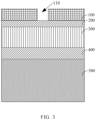
- the pattern sheet of the present embodiment includes a substrate 500, and a dielectric layer 400 and a mask structure sequentially arranged on the substrate 500 along a direction of the substrate 500.
- the mask layers may include three layers, which are a third mask layer 300, a second mask layer 200, and a first mask layer 100 sequentially stacked along a direction away from the substrate 500.
- the first mask layer 100 may be a photoresist layer.
- the photoresist layer may have a mask pattern composed of holes 110.
- the first mask layer 100 may be used as a mask for etching a through-hole in the second mask layer 200.
- the through-hole 210 formed in the second mask layer 200 are shown in FIG. 4A .
- the remaining thickness of the first mask layer 100 may be greater than zero. That is, when the through-hole 210 is formed, a certain thickness of the first mask layer 100 may still not be consumed, and the thickness of the second mask layer 120 may not be changed. In this situation, when the third mask layer 300 is etched, the remaining first mask layer 100 and the second mask layer 200 both may be used as masks for etching a through-hole in the third mask layer 300.
- the first mask layer 100 may be completely consumed while the second mask layer 200 is etched to form the through-hole 210 penetrating the thickness of the second mask layer 200, and the thickness of the second mask layer 200 may still be unchanged.
- the third mask layer 300 when the third mask layer 300 is etched, only the second mask layer 200 may be used as a mask for etching through-hole in the third mask layer 300.
- the first mask layer 100 is completely consumed. While the third mask layer 300 is etched to form the through-hole 310 penetrating the thickness of the third mask layer 300, the remaining thickness of the second mask layer 200 may be greater than zero. That is, when the through-hole 310 is formed, a certain thickness of the second mask layer 200 may still not be consumed. In this situation, when the dielectric layer 400 is etched, the remaining second mask layer 200 and the third mask layer 300 together may be used as masks for etching the through-hole in the dielectric layer 400.
- the remaining thickness of the second mask layer 200 may also be equal to zero.
- the dielectric layer 400 is etched, only the third mask layer 300 may be used as a mask for etching the through-hole in the dielectric layer 400.
- the second mask layer 200 may be completely consumed before the dielectric layer 400 is etched to form the through-hole 410 penetrating the thickness of the dielectric layer 400. While the dielectric layer 400 is etched to form the through-hole 410 penetrating the thickness of the dielectric layer 400, the remaining thickness of the third mask layer 300 may be greater than zero. That is, when the through-hole 410 is formed, a certain thickness of the third mask layer 300 may still not be consumed. In this situation, when the substrate 500 is etched, the remaining third mask layer 300 may be used as a mask for etching the hole in the substrate 500.
- the remaining thickness of the second mask layer 200 may also be greater than zero.
- the remaining second mask layer 200 and the third mask layer 300 may together be used as a mask for etching the hole in the substrate 500.
- the remaining thickness of the third mask layer 300 may be greater than zero.
- a certain thickness of the third mask layer 300 may remain to prevent the dielectric layer 400 from being etched to ensure that the dielectric layer is not damaged and has complete performance.
- the remaining thickness of the third mask layer 300 may also be equal to zero. That is, the third mask layer 300 may be completely consumed.
- the hole 510 of the set depth formed by etching the substrate 500 may be a blind hole with a depth smaller than the thickness of the substrate 500 or a through-hole penetrating the thickness of the substrate 500.
- the second mask layer 200 may include a material containing silicon, which has a good semiconductor property, is easy to obtain, and has low cost. Thus, processing difficulty and processing cost may be reduced. Moreover, when the substrate is etched using the second mask layer 200 as a mask, many materials can be used to etch the substrate and the second mask layer 200 simultaneously, which facilitates forming a hole with a greater depth in the substrate. In addition, in the situation that the second mask layer 200 includes the material containing silicon, the dielectric layer 400 and the substrate 500 may be etched sequentially by a fluorine-containing plasma. The dielectric layer 400 and the substrate 500 may be etched using the second mask layer 200 as a mask, which facilitates forming the through-holes penetrating the thicknesses of the dielectric layer 400 and the substrate 500 in the substrate 500 and dielectric layer 400.
- the second mask layer 200 may be a silicon dioxide layer, which can further reduce the material cost and processing difficulty of the second mask layer 200 and improve product competitiveness.
- the third mask layer 300 may be an APF ⁇ -C layer.
- the dielectric layer 400 and the substrate 500 can be etched sequentially by an oxygen-containing plasma.
- the dielectric layer 400 and the substrate 500 may be etched using the third mask layer 300 as the mask, which facilitates forming the through-holes penetrating the respective thicknesses of the substrate 500 and the dielectric layer 400 in the substrate 500 and the dielectric layer 400.
- the thickness of the first mask layer 100 may range from 1 ⁇ m to 2 ⁇ m.
- the thickness of the second mask layer 200 may range from 400 nm to 700 nm.
- the thickness of the third mask layer 300 may range from 6 ⁇ m to 7 ⁇ m. Within these thickness ranges, the hole with greater depth can be formed on the substrate to meet the application requirements.
- the respective thicknesses of the first mask layer 100, the second mask layer 200, and the third mask layer 300, and the etching selectivity ratios between the layers below each satisfy the following conditions: d 1 ′ ⁇ S 5 ′ > d 2 ′ , and d 2 ′ ⁇ S 6 ′ ⁇ d 3 ′ , and d3 ′ ⁇ d 1 ′ ⁇ d 4 ′ /S 3 ′ ⁇ S 2 ′ /S 1 ′ + d 4 ′ / S 4 ′ ; or, d 1 ′ ⁇ S 5 ′ ⁇ d 2 ′ , and d 2 ′ ⁇ S 6 ′ > d 3 ′ , and d 3 ′ ⁇ d 1 ′ ⁇ d 4 ′ / S 3 ′ ⁇ S 2 ′ / S 1 ′ + d 4 ′ / S 4 ′ ; or, d 1 ′ ⁇ S 5 ′ > d 2 ′ , and d
- the third mask layer 300 (or a portion of the first mask layer 100, the second mask layer 200, and the third mask layer 300, or a portion of the second mask layer 200 and the third mask layer 300) can be ensured to be used as the mask for etching the dielectric layer 400 and the substrate 500.
- the pattern sheet of the composite film layer can be used to form the hole with the greater depth on the substrate compared to using the photoresist alone as the pattern sheet of the dielectric layer and the substrate to meet the application requirements.
- the meaning represented by d1' ⁇ S5' may indicate that while the first mask layer 100 with the thickness of d1' is completely consumed, the thickness of the second mask layer 200 is dx.
- dx is equal to d2', it can be considered that while the first mask layer 100 with the thickness of d1' is completely consumed, the second mask layer 200 with the thickness of d2' may be also just completely consumed.
- d1' ⁇ S5' to be equal to d2', during the process of etching the second mask layer 200 using the first mask layer 100 as the mask, when the first mask layer 100 with the thickness of d1' is completely consumed, the through-hole 210 penetrating the thickness of the second mask layer 200 may be just formed.
- the pattern including the through-hole 210 that is formed on the second mask layer 200 may be eventually caused to be consistent with the mask pattern including the hole 110 on the first mask layer 100.
- the position of the through 210 may correspond to the position of the hole 110.
- d1' ⁇ S5' is greater than d2', it can be considered that during the process of etching the second mask layer 200 using the first mask layer 100 as the mask, while the through-hole 210 penetrating the thickness of the second mask layer 200 is formed on the second mask layer 200, the first mask layer 100 with the thickness of d1' may still remain.
- the second mask layer 200 and the remaining portion of the first mask layer 100 may be used as the mask together.
- the meaning represented by d2' ⁇ S6' may include that while the second mask layer 200 with the thickness of d2' is completely consumed, the thickness of the third mask layer 300 may have the thickness of dy.
- the second mask layer 200 with the thickness of d2' while the third mask layer 300 with the thickness of d3' may also be just completely consumed.
- the through-hole 310 penetrating the thickness of the third mask layer 300 may just be formed on the third mask layer 300.
- the position of the through-hole 310, the position of the through-hole 210, and the position of the hole 110 may correspond to each other by eventually causing the pattern including the through-hole 310 formed on the third mask layer 300 to be consistent with the mask pattern including the hole 110 on the first mask layer 100.
- d2' ⁇ S6'>d3' it can be considered that in the process of etching the third mask layer 300 by using the second mask layer 200 as the mask, when the through-hole 310 penetrating the thickness of the third mask layer 300 is just formed on the third mask layer 300, the second mask layer 200 with a thickness of d2' may still remain.
- the third mask layer 300 and a portion of the remaining second mask layer 200 may be used as the mask.
- d4'/S4' may represent that during the process of etching the dielectric layer 400 using the third mask layer 300 as the mask, when the through-hole 410 penetrating the thickness of the dielectric layer 400 is just formed in the dielectric layer 400 with the thickness of d4', the thickness of the third mask layer 300 may need to be consumed. Further, d3' -d4'/S4' may represent the remaining thickness of the third mask layer 300 when the through-hole 410 penetrating the thickness of the dielectric layer 400 is just formed in the dielectric layer 400 with the thickness of d4'.
- (d3'-d4'/ S4')/S2' may represent a depth of the thole formed in the substrate 500 when the third mask layer 300 with the thickness of d3'-d4'/ S4' is just completely consumed during the process of etching the substrate 500 by using the third mask layer 300 as the mask.
- d1'-d4'/S3' may represent the remaining thickness of the first mask layer 100 when the through-hole 410 penetrating the thickness of the dielectric layer 400 is just formed in the dielectric layer with the thickness of d4' during the process of etching the dielectric layer using the first mask layer 100 as the mask.
- (d1'-d4'/S3')/S1' may represent the depth of the hole formed in the substrate 500 when the first mask layer 100 with the thickness of d1'-d4'/S3' is just completely consumed during the process of etching the substrate 500 by using the first mask layer 100 as the mask.
- the depth of the hole eventually formed in the substrate 500 by only using the third mask layer 300 as the mask may be greater than the depth of the hole formed in the substrate 500 by using only the first mask layer 100 as the mask.
- the hole with a greater depth may have to be formed in the substrate 500 to satisfy the application requirements by comparing to etching the dielectric layer 400 and the substrate 500 only using the first mask layer 100 as the mask.
- the present embodiment provides a semiconductor intermediate product, which is formed by using an etching process on the pattern sheet of the above-mentioned embodiments of the present disclosure.
- the semiconductor intermediate product may include a substrate and a dielectric layer arranged on the substrate.
- the through-hole penetrating the thickness of the dielectric layer may be formed in the dielectric layer.
- the hole with the set depth corresponding to the through-hole may be formed in the substrate. While the substrate is etched to form the hole with the set depth, the remaining thickness of the mask layer located above the dielectric layer may be equal to zero, that is, may be completely consumed.
- the hole with the set depth formed in the substrate may be a blind-hole with the depth smaller than the thickness of the substrate or the through-hole penetrating the thickness of the substrate.
- the semiconductor intermediate product may further include a substrate, and a dielectric layer and a remaining mask layer of at least one layer after etching arranged on the substrate in sequence along a direction away from the substrate.
- Through-holes penetrating the thicknesses of the at least one layer of the mask layer and the dielectric layer may be formed correspondingly in the at least one layer of the mask layer and the dielectric layer.
- a hole with a set depth corresponding to the through-holes may be formed in the substrate.
- the remaining thickness of the mask layer above the dielectric layer may be greater than zero.
- FIG. 2D and FIG. 4D shows two semiconductor intermediate products, respectively, which retain the mask layer with the certain thickness while the hole with the set depth is formed in the substrate.
- This embodiment provides a hole etching method, which uses the pattern sheets provided by the above-mentioned embodiments of the present disclosure to etch the substrate and the dielectric layer arranged on the substrate to form corresponding holes.
- the hole etching method includes:
- the hole etching method provided by the embodiment may be applied to a through silicon vias (TSV) etching process to further reduce the processing difficulty and improve the processing efficiency.
- TSV through silicon vias
- the thicknesses of the layers of the mask layer and the etching selectivity ratios between the layers below the mask layer satisfy that, during the process of etching the substrate and the dielectric layer to form holes correspondingly by using the mask structure, in each two neighboring layers of the mask layer, while the lower layer of the mask layer is etched to form a through-hole penetrating the thickness of the lower layer of the mask layer, the remaining thickness of the upper layer of the mask layer may be greater than or equal to zero, and while the dielectric layer is etched to form the through-hole penetrating the thickness of the dielectric layer, a sum of the remaining thicknesses of all the layers of the mask layer above the dielectric layer may
Landscapes
- Drying Of Semiconductors (AREA)
- Internal Circuitry In Semiconductor Integrated Circuit Devices (AREA)
Abstract
Description
- The present disclosure generally relates to the field of semiconductor equipment, and more particularly, to a pattern sheet, semiconductor intermediate product, and hole etching method.
- Affected by user requirements, integrated circuit (IC) manufacturing has shifted from two-dimensional (2D) planar integrated manufacturing technology to three-dimensional (3D) stereoscopic integrated manufacturing technology. In the 3D stereoscopic three-dimensional integrated manufacturing technology, etching technology can be used to form a through-hole between a substrate and a substrate to make the substrates vertically conductive. The substrates can be silicon substrates (wafers). Specifically, the surface of the substrates is generally provided with a complementary metal-oxide-semiconductor (hereinafter referred to as CMOS) dielectric layer. During a process of forming the through-hole, the CMOS dielectric layer needs to be etched first to form the through-hole penetrating the CMOS dielectric layer. Then, the substrate is etched to form a through-hole penetrating the substrate.
- Currently, a mask used in the etching process is generally a photoresist mask. Since the photoresist mask is usually formed on a side of the CMOS dielectric layer away from the substrate, the photoresist mask has to play a mask function for the CMOS dielectric layer and the substrate. However, due to the limitation of the exposure energy and accuracy of the photolithography technology, a thickness of the photoresist mask needs to be smaller than a size of a mask opening, which causes an upper limitation for a thickness of the photoresist mask and cannot satisfy thickness requirements of the photoresist mask for a hole with a relatively small diameter (such as 2~5 µm) and a relatively large depth.
- The present disclosure provides a pattern sheet and a hole etching method, with which a hole with a larger depth can be formed in a substrate to meet application requirements.
- In order to solve the above problems, the present disclosure adopts the following technical solutions.
- Embodiments of the present disclosure provide a pattern sheet, including a substrate, and a dielectric layer and a mask structure sequentially arranged on the substrate along a direction away from the substrate. The mask structure includes a multi-layer mask layer sequentially arranged in stacks from a side of the dielectric layer away from the substrate and along a direction away from the substrate. An uppermost layer of the mask layer is a photoresist layer. A thickness of each layer of the mask layer and etching selectivity ratios between layers below the mask layer satisfy that, during a process of etching the substrate and the dielectric layer to form holes correspondingly by using the mask structure, in each two neighboring layers of the mask layer, while a lower layer of the mask layer is etched to form a through-hole penetrating a thickness of the lower layer, a remaining thickness of an upper layer of the mask layer is greater than or equal to zero, while the dielectric layer is etched to form a through-hole penetrating a thickness of the dielectric layer, a remaining thickness of all the mask layer above the dielectric layer is greater than zero, and while a hole with a set depth is formed in the substrate, the remaining thickness of all the mask layer above the dielectric layer is greater than or equal to zero.
- In some embodiments, a number of layers of the mask layer is two, which are a second mask layer and a first mask layer sequentially stacked along the direction away from the substrate. The first mask layer is the photoresist layer. Respective thicknesses of the first mask layer and the second mask layer and etching selectivity ratios between layers below the mask layer satisfy the following conditions:


- In some embodiments, the second mask layer includes a material containing silicon.
- In some embodiments, the second mask layer is a silicon dioxide layer.
- In some embodiments, a number of layers of the mask layer is three, which are a third mask layer, a second mask layer, and a first mask layer sequentially stacked along the direction away from the substrate. The first mask layer is the photoresist layer. Respective thicknesses of the first mask layer, the second mask layer, and the third mask layer and etching selectivity ratios between the layers below the mask layer satisfy the following conditions:


- In some embodiments, the second mask layer is a silicon dioxide layer.
- In some embodiments, the third mask layer is an APFα-C layer.
- In some embodiments, the thickness of the first mask layer ranges from 1 µm to 2 µm, the thickness of the second mask layer ranges from 400 nm to 700 nm, and the thickness of the third mask layer ranges from 6 µm to 7 µm.
- As another technical solution, embodiments of the present disclosure provide a semiconductor intermediate product, which is formed from the pattern sheet of embodiments of the present disclosure by an etching process. The semiconductor intermediate product includes a substrate and a dielectric layer arranged on the substrate or a substrate and a dielectric layer and a remaining mask layer with at least one layer after etching arranged sequentially on the substrate along the direction away from the substrate. Through-holes penetrating thicknesses of the mask layer with the at least one layer and the dielectric layer are formed in the mask layer with the at least one layer and the dielectric layer, and a hole with a set depth is formed in the substrate.
- As another technical solution, embodiments of the present disclosure provide a hole etching method. The substrate and the dielectric layer arranged on the substrate are etched to form the corresponding holes by using the pattern sheet of embodiments of the present disclosure. The hole etching method includes:
- etching a lower layer of a mask layer to form a through-hole penetrating a thickness of the lower layer of the mask layer by using an upper layer of any two neighboring layers of the mask layer as a mask; and
- etching a dielectric layer to form a through-hole penetrating a thickness of the dielectric layer and forming a hole with a set depth in the substrate by using the remaining mask layer with at least one layer above the dielectric layer.
- In some embodiments, the hole etching method is applied to a through silicon via (TSV) etching process.
- The technical solutions adopted in the present disclosure can achieve the following beneficial effects.
- The present disclosure provides the technical solutions for the pattern sheet, a semiconductor intermediate product, and a hole etching method. By using the mask structure of the composite film layer, that is, the multi-layer mask layer stacked sequentially from the side of the dielectric layer away from the substrate and along the direction away from the substrate, the thickness of each layer of the mask layer and the etching selectivity ratios between the layers below the mask layer satisfy that, during the process of etching the substrate and the dielectric layer to form the holes correspondingly using the mask structure, in each of the two neighboring layers of the mask layer, while the lower layer of the mask layer is etched to form the through-hole penetrating the thickness of the lower layer of the mask layer, the remaining thickness of the upper layer of the mask layer is greater than or equal to zero. While the dielectric layer is etched to form the through-hole penetrating the thickness of the dielectric layer, the remaining thickness of all the mask layer above the dielectric layer is greater than zero. While the hole with the set depth is formed in the substrate, the remaining thickness of all the mask layer above the dielectric layer is greater than or equal to zero. Thus, compared to using the photoresist mask alone in the existing technology, by using the pattern sheet of the mask structure having the composite film layer, the hole with the greater depth is formed in the substrate to satisfy the application requirements.
- The accompanying drawings described herein are used to provide further understanding of the present disclosure and constitute a part of the present disclosure. Exemplary embodiments of the present disclosure and their descriptions are used to explain the present disclosure and do not constitute an improper limitation of the present disclosure. In the accompanying drawings:
-
FIG. 1 is a schematic cross-section diagram of a pattern sheet according to a first embodiment of the present disclosure; -
FIG. 2A is a schematic cross-section diagram showing a pattern sheet after a second mask layer is etched to form a through-hole according to a first embodiment of the present disclosure; -
FIG. 2B is a schematic cross-section diagram showing a pattern sheet after a dielectric layer is etched to form a through-hole according to a first embodiment of the present disclosure; -
FIG. 2C is a schematic cross-section diagram of a semiconductor intermediate product according to a first embodiment of the present disclosure; -
FIG. 3 is a schematic cross-section diagram of a pattern sheet according to a second embodiment of the present disclosure; -
FIG. 4A is a schematic cross-section diagram of a pattern sheet after a second mask layer is etched to form a through-hole according to a second embodiment of the present disclosure; -
FIG. 4B is a schematic cross-section diagram of a pattern sheet after a third mask layer is etched to form a through-hole according to a second embodiment of the present disclosure; -
FIG. 4C is a schematic cross-section diagram of a pattern sheet after a dielectric layer is etched to form a through-hole according to a second embodiment of the present disclosure; and -
FIG. 4D is a schematic cross-section diagram of a semiconductor intermediate product according to a second embodiment of the present disclosure. - In order to make the objectives, technical solutions, and advantages of the present disclosure clearer, the technical solutions of the present disclosure will be clearly and completely described below with reference to specific embodiments of the present disclosure and the corresponding accompanying drawings. Obviously, the described embodiments are only some, but not all, embodiments of the present disclosure. Based on embodiments of the present disclosure, all other embodiments obtained by those of ordinary skill in the art without creative efforts shall fall within the protection scope of the present disclosure.
- The technical solutions disclosed by embodiments of the present disclosure will be described in detail below with reference to the accompanying drawings.
- The present disclosure provides a pattern sheet, which includes a substrate, and a dielectric layer and a mask structure sequentially arranged on the substrate along a direction of the substrate. A pattern consisting of holes may be formed on the dielectric layer and the substrate by performing an etching process using the mask structure. The etching process may include, for example, a through silicon via (TSV) process. The substrate may be a silicon substrate. The dielectric layer may be, for example, a CMOS dielectric layer. A CMOS circuit may be arranged on the dielectric layer.
- The above-mentioned mask structure includes a multi-layer mask layer, which is arranged from a side of the dielectric layer away from the substrate and is sequentially stacked along a direction away from the substrate. An uppermost mask layer may be a photoresist layer. The photoresist layer may include a mask pattern consisting of holes. The mask pattern can be formed by exposure. The holes in the mask pattern can be circular holes. Radii of the holes can be determined according to actual needs. Of course, the holes can also be set to holes with any other shapes. In addition, by changing exposure energy, a through-hole penetrating the thickness of the mask layer can be formed in the uppermost mask layer whose thickness satisfies the requirements. In a process of performing the etching process using the mask structure, at least one layer of the mask layer can be etched located below the mask layer using the uppermost mask layer as the mask. It should be noted that, before the above-mentioned etching process is performed, no pattern corresponding to the above-mentioned mask pattern may be formed on other film layers except the photoresist layer.
- Moreover, a thickness of each layer of the mask layer and an etching selectivity ratio between the layers below the mask layer may satisfy that, in an etching process of forming the hole in the substrate and the dielectric layer using the above mask structure correspondingly, in each of two neighboring layers of the mask layer, while a lower portion of the mask layer is etched to form a through-hole penetrating a thickness of the lower portion, the remaining thickness of an upper portion of the mask layer may be greater than or equal to zero. While the dielectric layer is etched to form a through-hole penetrating the thickness of the dielectric layer, the remaining thicknesses of all mask layers above the dielectric layer may be greater than zero. While a hole with a set depth is formed in the substrate, the remaining thicknesses of all mask layers above the dielectric layer are greater than or equal to zero. That is, each layer of the mask layer can be used as a mask for etching a lower layer neighboring to the layer of the mask layer to form the through-hole. When the substrate is etched, a sum of the remaining thickness of all mask layers above the dielectric layer is large enough to cause the hole formed in the substrate to reach the set depth.
- As can be seen from the above, compared with using the photoresist mask alone in the existing technology, using the pattern sheet with the above-mentioned mask structure with the multi-film layers, a hole with a larger depth can be formed on the substrate to meet the usage requirements.
- A specific implementation of the above-mentioned pattern sheet will be described in detail below.
- Referring to
FIG. 1 , the pattern sheet of the present embodiment includes asubstrate 50, and adielectric layer 40 and a mask structure sequentially arranged on thesubstrate 50 along a direction away from thesubstrate 50. In the mask structure, the mask layer includes two layers, which are asecond mask layer 20 and afirst mask layer 10 which are stacked in sequence along the direction away from thesubstrate 50. Thefirst mask layer 10 may be a photoresist layer, and the photoresist layer has a mask pattern composed of ahole 11. In addition, thefirst mask layer 10 may be used as a mask for etching a through-hole in thesecond mask layer 20. A through-hole 21 formed in thesecond mask layer 20 is shown inFIG. 2A . In the present embodiment, while thesecond mask layer 20 is etched to form the through-hole 21 penetrating the thickness of thesecond mask layer 20, the remaining thickness of thefirst mask layer 10 may be greater than zero. That is, when the through-hole 21 is formed, a certain thickness of thefirst mask layer 10 may not be consumed. The thickness of thesecond mask layer 20 may be unchanged. In this situation, when thedielectric layer 40 is etched, the remainingfirst mask layer 10 and thesecond mask layer 20 may both be used as masks for etching a through-hole in thedielectric layer 40. - Of course, in other embodiments of the present disclosure, the
first mask layer 10 may be completely consumed while thesecond mask layer 20 is etched to form the through-hole 21 penetrating the thickness of thesecond mask layer 20, and thesecond mask layer 20 may still remain unchanged. In this case, when thedielectric layer 40 is etched, only thesecond mask layer 20 may be used as a mask for etching the through-hole in thedielectric layer 40. - As shown in
FIG. 2B , before thedielectric layer 40 is etched to form the through-hole 41 penetrating the thickness of thedielectric layer 40, thefirst mask layer 10 is completely consumed. While thedielectric layer 40 is etched to form the through-hole 41 penetrating the thickness of thedielectric layer 40, the remaining thickness of thesecond mask layer 20 may be greater than zero. That is, when the through-hole 41 is formed, a certain thickness of thesecond mask layer 20 may still not be consumed. In this situation, when thesubstrate 50 is etched, the remainingsecond mask layer 20 may be used as a mask for etching a hole in thesubstrate 50. - Of course, in other embodiments of the present disclosure, while the
dielectric layer 40 is etched to form the through-hole 41 penetrating the thickness of thedielectric layer 40, the remaining thickness of thefirst mask layer 10 may also be greater than zero. In this situation, when thesubstrate 50 is etched, the remainingfirst mask layer 10 and thesecond mask layer 20 may both be used as the masks for etching the hole in thesubstrate 50. - As shown in
FIG. 2C , while thehole 51 with the set depth is formed by etching in thesubstrate 50, the remaining thickness of thesecond mask layer 20 is greater than zero. Thus, while the hole with the set depth is formed in thesubstrate 50, a certain thickness of thesecond mask layer 20 may still remain to prevent thedielectric layer 40 from being etched to ensure that the dielectric layer is not damaged and has complete performance. Of course, in other embodiments of the present disclosure, while thehole 51 with the set depth is formed by etching in thesubstrate 50, the remaining thickness of thesecond mask layer 20 may also be equal to zero. That is, thesecond mask layer 20 may be completely consumed. In addition, thehole 51 with the set depth formed by etching in thesubstrate 50 may be a blind hole with a depth smaller than the thickness of thesubstrate 50 or may be a through-hole penetrating the thickness of thesubstrate 50. - Based on the above embodiment, in some embodiments, the
second mask layer 20 includes a material containing silicon. The silicon has good semiconductor properties, is easy to obtain, and has a low cost. Thus, the processing difficulty and processing cost may be reduced. In addition, in the process of performing the etching on the substrate using thesecond mask layer 20 as a mask, many materials may be used to etch thesecond mask layer 20 and the substrate, which is beneficial to form a hole with a relatively large depth in the substrate. In addition, in the situation that thesecond mask layer 20 includes a material containing silicon, etching may be performed on thedielectric layer 40 and thesubstrate 50 in sequence by fluorine-containing plasma. Thesecond mask layer 20 may be used as the mask for etching thedielectric layer 40 and thesubstrate 50, which facilitates the formation of the holes penetrating the respective thicknesses of thesubstrate 50 and thedielectric layer 40. - Further, in some embodiments, the
second mask layer 20 may be a silicon dioxide layer, which can further reduce the material cost and processing difficulty of thesecond mask layer 20 and improve product competitiveness. - In addition, the respective thicknesses of the
first mask layer 10 and thesecond mask layer 20 and the etching selectivity ratio between the layers below each satisfy the following conditions:

first mask layer 10, d2 denotes a thickness of thesecond mask layer 20, d4 denotes a thickness of thedielectric layer 40, S1 denotes an etching selectivity ratio between thesubstrate 50 and thefirst mask layer 10, S2 denotes an etching selectivity ratio between thesubstrate 50 and thesecond mask layer 20, S3 denotes an etching selectivity ratio between thedielectric layer 40 and thefirst mask layer 10, S4 denotes an etching selectivity ratio between thedielectric layer 40 and thesecond mask layer 20, and S5 denotes an etching selectivity ratio between thesecond mask layer 20 and thefirst mask layer 10. - It should be noted that the etching selectivity ratio may be used to indicate a relative etching rate of one material relative to another material under the same etching condition. For example, etching selectivity ratio S1 between the
substrate 50 and thefirst mask layer 10 may indicate a ratio of an etching rate of thesubstrate 50 to an etching rate of thefirst mask layer 10 under the same etching condition, when thefirst mask layer 10 is used as a mask, and thesubstrate 50 is used as the material to be etched. - By making the respective thicknesses of the
first mask layer 10 and thesecond mask layer 20 and the etching selectivity ratio between the layers below each satisfy the above conditions, a portion of thefirst mask layer 10 and thesecond mask layer 20 can be used as a mask for etching the dielectric layer 40 (or etching thedielectric layer 40 and the substrate 50). With the mask structure of the composite film layer compared to using the photoresist alone as the mask structure of the dielectric layer and the substrate, a hole with larger depth may be formed on the substrate to satisfy application needs. - In detail, the meaning represented by d1×S5 is that while the
first mask layer 10 with a thickness of d1 is completely consumed, the thickness of thesecond mask layer 20 is consumed by dx. When dx is equal to d2, it can be considered that while thefirst mask layer 10 with the thickness of d1 is completely consumed, the second mask layer with the thickness of d2 may be also completely consumed. Based on this, by causing d1×S5 to be equal to d2, during a process of etching thesecond mask layer 20 using thefirst mask layer 10, when the first mask layer with the thickness d1 is completely consumed, a through-hole 21 penetrating the thickness of thesecond mask layer 20 may be just formed. It is easy to understand that the pattern including the through-hole 21 formed on thesecond mask layer 20 is consistent with the mask pattern including thehole 11 on thefirst mask layer 10. The position of the through-hole 21 may correspond to the position of thehole 11. Obviously, when d1×S5 is greater than d2, it can be considered that in the process of etching thesecond mask layer 20 by using thefirst mask layer 10 as a mask, while the through-hole 21 penetrating the thickness of thesecond mask layer 20 is formed on thesecond mask layer 20, thefirst mask layer 10 with the thickness of d1 still remains. Thus, during the process of etching the dielectric layer 40 (or thedielectric layer 40 and the substrate 50), the remaining portions of thesecond mask layer 20 and thefirst mask layer 10 may be used as the mask.
d2=(d1-d4/S3)×S2/S1+d4/S4, that is, it can be deduced as d2-d4/S4=(d1-d4/S3)×S2/S1, or it can be further deduced as (d2-d4/S4) /S2=(d1-d4/S3)/S1. - In the above equation (d2-d4/S4)/S2=(d1-d4/S3)/S1, d4/S4 may indicate that in the process of etching the
dielectric layer 40 by using thesecond mask layer 20 as the mask, the thickness of thesecond mask layer 20 may need to be consumed when the through-hole 41 penetrating the thickness of thedielectric layer 40 is formed in thedielectric layer 40 with the thickness of d4. Further, d2-d4/S4 may indicate the remaining thickness of thesecond mask layer 20 when the through-hole 41 penetrating the thickness of thedielectric layer 40 is just formed in thedielectric layer 40 with the thickness of d4. Furthermore, (d2-d4/S4)/S2 may indicate the depth of the hole formed in thesubstrate 50 in the process of etching thesubstrate 50 using thesecond mask layer 20 as the mask when thesecond mask layer 20 with the thickness of d2-d4/S4 is just completely consumed. - Similarly, d1-d4/S3 may indicate a remaining thickness of the
first mask layer 10 in the process of etching thedielectric layer 40 by using thefirst mask layer 10 as the mask, when the through-hole 41 penetrating the thickness of thedielectric layer 40 is just formed in thedielectric layer 40 with the thickness of d4. Further, (d1-d4/S3)/S 1 may indicate a depth of the hole formed in thesubstrate 50 in the process of etching thesubstrate 50 by using thefirst mask layer 10 as the mask when thefirst mask layer 10 with the thickness of d1-d4/S3 is just completely consumed. - Obviously, when (d2-d4/S4)/S2 is equal to (d1-d4/S3)/S1, it can be considered that the
dielectric layer 40 and thesubstrate 50 may be etched only by using thesecond mask layer 20 as the mask compared to etching thedielectric layer 40 and thesubstrate 50 only by using thefirst mask layer 10 as the mask, the depths of the holes formed in thesubstrate 50 by the two may be equal. When (d2-d4/S4)/S2 is greater than (d1-d4/S3)/S1, that is, d2 is greater than (d1-d4/S3)×S2/S1+d4/S4, the depth of the hole eventually formed in thesubstrate 50 by only using thesecond mask layer 20 as the mask may be greater than the depth of the hole eventually formed in thesubstrate 50 by only using thefirst mask layer 10 as the mask. - Therefore, when the respective thicknesses of the
first mask layer 10 and thesecond mask layer 20 and the etching selectivity ratios between the layers below each satisfy the conditions of d1×S5>d2 and d2≥(d1- d4/S3)×S2/S1+d4/S4, in the process of etching the dielectric layer 40 (or thedielectric layer 40 and the substrate 50), thedielectric layer 40 may be etched using the remaining portions of thesecond mask layer 20 and thefirst mask 10 as the mask. Compared to etching thedielectric layer 40 and thesubstrate 50 only using thefirst mask layer 10 as the mask, the hole with a greater depth may be formed in thesubstrate 50 to satisfy the application needs. When the respective thicknesses of thefirst mask layer 10 and thesecond mask layer 20 and the etching selectivity ratios of the layers below each satisfy the conditions of d1×S5=d2 and d2>(d1-d4/S3)×S2/S1+d4/S4, as mentioned above, the depth of the hole eventually formed in thesubstrate 50 by only using thesecond mask layer 20 as the mask may be greater than the depth of the hole eventually formed in thesubstrate 50 by only using thefirst mask layer 10 as the mask to satisfy the application requirements. - Referring to
FIG. 3 , the pattern sheet of the present embodiment includes asubstrate 500, and adielectric layer 400 and a mask structure sequentially arranged on thesubstrate 500 along a direction of thesubstrate 500. In the mask structure, the mask layers may include three layers, which are athird mask layer 300, asecond mask layer 200, and afirst mask layer 100 sequentially stacked along a direction away from thesubstrate 500. Thefirst mask layer 100 may be a photoresist layer. The photoresist layer may have a mask pattern composed ofholes 110. In addition, thefirst mask layer 100 may be used as a mask for etching a through-hole in thesecond mask layer 200. The through-hole 210 formed in thesecond mask layer 200 are shown inFIG. 4A . In the present embodiment, while thesecond mask layer 200 is etched to form the through-hole 210 penetrating the thickness of thesecond mask layer 200, the remaining thickness of thefirst mask layer 100 may be greater than zero. That is, when the through-hole 210 is formed, a certain thickness of thefirst mask layer 100 may still not be consumed, and the thickness of the second mask layer 120 may not be changed. In this situation, when thethird mask layer 300 is etched, the remainingfirst mask layer 100 and thesecond mask layer 200 both may be used as masks for etching a through-hole in thethird mask layer 300. - Of course, in other embodiments of the present disclosure, the
first mask layer 100 may be completely consumed while thesecond mask layer 200 is etched to form the through-hole 210 penetrating the thickness of thesecond mask layer 200, and the thickness of thesecond mask layer 200 may still be unchanged. In this situation, when thethird mask layer 300 is etched, only thesecond mask layer 200 may be used as a mask for etching through-hole in thethird mask layer 300. - As shown in
FIG. 4B , before thethird mask layer 300 is etched to form the through-hole 310 penetrating the thickness of thethird mask layer 300, thefirst mask layer 100 is completely consumed. While thethird mask layer 300 is etched to form the through-hole 310 penetrating the thickness of thethird mask layer 300, the remaining thickness of thesecond mask layer 200 may be greater than zero. That is, when the through-hole 310 is formed, a certain thickness of thesecond mask layer 200 may still not be consumed. In this situation, when thedielectric layer 400 is etched, the remainingsecond mask layer 200 and thethird mask layer 300 together may be used as masks for etching the through-hole in thedielectric layer 400. - Of course, in other embodiments of the present disclosure, while the
third mask layer 300 is etched to form the through-hole 310 penetrating the thickness of thethird mask layer 300, the remaining thickness of thesecond mask layer 200 may also be equal to zero. In this situation, when thedielectric layer 400 is etched, only thethird mask layer 300 may be used as a mask for etching the through-hole in thedielectric layer 400. - As shown in
FIG. 4C , before thedielectric layer 400 is etched to form the through-hole 410 penetrating the thickness of thedielectric layer 400, thesecond mask layer 200 may be completely consumed. While thedielectric layer 400 is etched to form the through-hole 410 penetrating the thickness of thedielectric layer 400, the remaining thickness of thethird mask layer 300 may be greater than zero. That is, when the through-hole 410 is formed, a certain thickness of thethird mask layer 300 may still not be consumed. In this situation, when thesubstrate 500 is etched, the remainingthird mask layer 300 may be used as a mask for etching the hole in thesubstrate 500. - Of course, in other embodiments of the present disclosure, while the
dielectric layer 400 is etched to form the through-hole 410 penetrating the thickness of thedielectric layer 400, the remaining thickness of thesecond mask layer 200 may also be greater than zero. In this situation, when thesubstrate 500 is etched, the remainingsecond mask layer 200 and thethird mask layer 300 may together be used as a mask for etching the hole in thesubstrate 500. - As shown in
FIG. 4D , while thesubstrate 500 is etched to form thehole 510 of the set depth, the remaining thickness of thethird mask layer 300 may be greater than zero. Thus, while the hole of the set depth is formed in thesubstrate 500, a certain thickness of thethird mask layer 300 may remain to prevent thedielectric layer 400 from being etched to ensure that the dielectric layer is not damaged and has complete performance. Of course, in other embodiments of the present disclosure, while thesubstrate 500 is etched to form thehole 510 with the set depth, the remaining thickness of thethird mask layer 300 may also be equal to zero. That is, thethird mask layer 300 may be completely consumed. In addition, thehole 510 of the set depth formed by etching thesubstrate 500 may be a blind hole with a depth smaller than the thickness of thesubstrate 500 or a through-hole penetrating the thickness of thesubstrate 500. - The
second mask layer 200 may include a material containing silicon, which has a good semiconductor property, is easy to obtain, and has low cost. Thus, processing difficulty and processing cost may be reduced. Moreover, when the substrate is etched using thesecond mask layer 200 as a mask, many materials can be used to etch the substrate and thesecond mask layer 200 simultaneously, which facilitates forming a hole with a greater depth in the substrate. In addition, in the situation that thesecond mask layer 200 includes the material containing silicon, thedielectric layer 400 and thesubstrate 500 may be etched sequentially by a fluorine-containing plasma. Thedielectric layer 400 and thesubstrate 500 may be etched using thesecond mask layer 200 as a mask, which facilitates forming the through-holes penetrating the thicknesses of thedielectric layer 400 and thesubstrate 500 in thesubstrate 500 anddielectric layer 400. - Further, in some embodiments, the
second mask layer 200 may be a silicon dioxide layer, which can further reduce the material cost and processing difficulty of thesecond mask layer 200 and improve product competitiveness. - In some embodiments, the
third mask layer 300 may be an APFα-C layer. In the situation that thethird mask layer 300 is the APFα-C layer, thedielectric layer 400 and thesubstrate 500 can be etched sequentially by an oxygen-containing plasma. Thedielectric layer 400 and thesubstrate 500 may be etched using thethird mask layer 300 as the mask, which facilitates forming the through-holes penetrating the respective thicknesses of thesubstrate 500 and thedielectric layer 400 in thesubstrate 500 and thedielectric layer 400. - In some embodiments, the thickness of the
first mask layer 100 may range from 1 µm to 2 µm. The thickness of thesecond mask layer 200 may range from 400 nm to 700 nm. The thickness of thethird mask layer 300 may range from 6 µm to 7 µm. Within these thickness ranges, the hole with greater depth can be formed on the substrate to meet the application requirements. - In addition, the respective thicknesses of the first mask layer 100, the second mask layer 200, and the third mask layer 300, and the etching selectivity ratios between the layers below each satisfy the following conditions:


- By making the respective thicknesses of the
first mask layer 100, thesecond mask layer 200, and thethird mask layer 300, and the etching selectivity ratios between the layers below thefirst mask layer 100, thesecond mask layer 200, and thethird mask layer 300 satisfy the above conditions, the third mask layer 300 (or a portion of thefirst mask layer 100, thesecond mask layer 200, and thethird mask layer 300, or a portion of thesecond mask layer 200 and the third mask layer 300) can be ensured to be used as the mask for etching thedielectric layer 400 and thesubstrate 500. The pattern sheet of the composite film layer can be used to form the hole with the greater depth on the substrate compared to using the photoresist alone as the pattern sheet of the dielectric layer and the substrate to meet the application requirements. - In detail, the meaning represented by d1'×S5' may indicate that while the
first mask layer 100 with the thickness of d1' is completely consumed, the thickness of thesecond mask layer 200 is dx. When dx is equal to d2', it can be considered that while thefirst mask layer 100 with the thickness of d1' is completely consumed, thesecond mask layer 200 with the thickness of d2' may be also just completely consumed. Based on this, by cause d1'×S5' to be equal to d2', during the process of etching thesecond mask layer 200 using thefirst mask layer 100 as the mask, when thefirst mask layer 100 with the thickness of d1' is completely consumed, the through-hole 210 penetrating the thickness of thesecond mask layer 200 may be just formed. It is easy to understand that the pattern including the through-hole 210 that is formed on thesecond mask layer 200 may be eventually caused to be consistent with the mask pattern including thehole 110 on thefirst mask layer 100. The position of the through 210 may correspond to the position of thehole 110. Obviously, when d1'×S5' is greater than d2', it can be considered that during the process of etching thesecond mask layer 200 using thefirst mask layer 100 as the mask, while the through-hole 210 penetrating the thickness of thesecond mask layer 200 is formed on thesecond mask layer 200, thefirst mask layer 100 with the thickness of d1' may still remain. Thus, during the process of etching thedielectric layer 400 and thesubstrate 500, thesecond mask layer 200 and the remaining portion of thefirst mask layer 100 may be used as the mask together. - The meaning represented by d2'×S6' may include that while the
second mask layer 200 with the thickness of d2' is completely consumed, the thickness of thethird mask layer 300 may have the thickness of dy. When dy is equal to d3', thesecond mask layer 200 with the thickness of d2' while thethird mask layer 300 with the thickness of d3' may also be just completely consumed. Based on this, by causing d2'×S6' to be equal to d3', during the process of etching thethird mask layer 300 using thesecond mask layer 200 as the mask, when thesecond mask layer 200 with the thickness of d2' is also just completely consumed, the through-hole 310 penetrating the thickness of thethird mask layer 300 may just be formed on thethird mask layer 300. It can be easily understood that the position of the through-hole 310, the position of the through-hole 210, and the position of thehole 110 may correspond to each other by eventually causing the pattern including the through-hole 310 formed on thethird mask layer 300 to be consistent with the mask pattern including thehole 110 on thefirst mask layer 100. Obviously, when d2'×S6'>d3', it can be considered that in the process of etching thethird mask layer 300 by using thesecond mask layer 200 as the mask, when the through-hole 310 penetrating the thickness of thethird mask layer 300 is just formed on thethird mask layer 300, thesecond mask layer 200 with a thickness of d2' may still remain. Thus, during the process of etching thedielectric layer 400 and thesubstrate 500, thethird mask layer 300 and a portion of the remainingsecond mask layer 200 may be used as the mask.
d3'=(d1'-d4'/S3')×S2'/S1'+d4'/S4', which can be derived as d3'-d4'/S4'=(d1'-d4'/S3')×S2 '/S1', and can also be further derived as (d3'-d4'/S4')/S2'=(d1'-d4'/S3')/S1'. - In the above equation (d3'-d4'/S4')/S2'=(d1'-d4'/S3')/S1', d4'/S4' may represent that during the process of etching the
dielectric layer 400 using thethird mask layer 300 as the mask, when the through-hole 410 penetrating the thickness of thedielectric layer 400 is just formed in thedielectric layer 400 with the thickness of d4', the thickness of thethird mask layer 300 may need to be consumed. Further, d3' -d4'/S4' may represent the remaining thickness of thethird mask layer 300 when the through-hole 410 penetrating the thickness of thedielectric layer 400 is just formed in thedielectric layer 400 with the thickness of d4'. Further more, (d3'-d4'/ S4')/S2' may represent a depth of the thole formed in thesubstrate 500 when thethird mask layer 300 with the thickness of d3'-d4'/ S4' is just completely consumed during the process of etching thesubstrate 500 by using thethird mask layer 300 as the mask. - Similarly, d1'-d4'/S3' may represent the remaining thickness of the
first mask layer 100 when the through-hole 410 penetrating the thickness of thedielectric layer 400 is just formed in the dielectric layer with the thickness of d4' during the process of etching the dielectric layer using thefirst mask layer 100 as the mask. Further, (d1'-d4'/S3')/S1' may represent the depth of the hole formed in thesubstrate 500 when thefirst mask layer 100 with the thickness of d1'-d4'/S3' is just completely consumed during the process of etching thesubstrate 500 by using thefirst mask layer 100 as the mask. - Obviously, when (d3'-d4'/S4')/S2'=(d1'-d4'/S3')/S1', it can be considered that, by comparing etching the
dielectric layer 400 and thesubstrate 500 only using thethird mask layer 300 as the mask to etching thedielectric layer 400 and thesubstrate 500 only using thefirst mask layer 100, the depths of the holes formed in thesubstrate 500 may be equal to each other. When (d3'-d4'/S4')/S2'>(d1'-d4'/S3')/S1', that is, d3'>(d1'-d4'/S3')×S2'/S1'+ d4'/S4', the depth of the hole eventually formed in thesubstrate 500 by only using thethird mask layer 300 as the mask may be greater than the depth of the hole formed in thesubstrate 500 by using only thefirst mask layer 100 as the mask. - It can be seen from the above that, similar to the above-mentioned first embodiment, when the respective thicknesses of the
first mask layer 100, thesecond mask layer 200, and thethird mask layer 300, and the etching selectivity ratios between the layers below them satisfy the above conditions, the hole with a greater depth may have to be formed in thesubstrate 500 to satisfy the application requirements by comparing to etching thedielectric layer 400 and thesubstrate 500 only using thefirst mask layer 100 as the mask. - The present embodiment provides a semiconductor intermediate product, which is formed by using an etching process on the pattern sheet of the above-mentioned embodiments of the present disclosure. Specifically, the semiconductor intermediate product may include a substrate and a dielectric layer arranged on the substrate. The through-hole penetrating the thickness of the dielectric layer may be formed in the dielectric layer. The hole with the set depth corresponding to the through-hole may be formed in the substrate. While the substrate is etched to form the hole with the set depth, the remaining thickness of the mask layer located above the dielectric layer may be equal to zero, that is, may be completely consumed. In addition, the hole with the set depth formed in the substrate may be a blind-hole with the depth smaller than the thickness of the substrate or the through-hole penetrating the thickness of the substrate.
- Alternatively, the semiconductor intermediate product may further include a substrate, and a dielectric layer and a remaining mask layer of at least one layer after etching arranged on the substrate in sequence along a direction away from the substrate. Through-holes penetrating the thicknesses of the at least one layer of the mask layer and the dielectric layer may be formed correspondingly in the at least one layer of the mask layer and the dielectric layer. A hole with a set depth corresponding to the through-holes may be formed in the substrate. In the process of performing the etching process using the above-mentioned pattern sheet of embodiments of the present disclosure, while the substrate is etched to form the hole with the set depth, the remaining thickness of the mask layer above the dielectric layer may be greater than zero. Thus, while the hole with the set depth is formed in the substrate, the mask layer with a certain thickness may still remain, which can prevent the dielectric layer from being etched to ensure that the dielectric layer is not damaged and has complete performance. For example, FIG. 2D and
FIG. 4D shows two semiconductor intermediate products, respectively, which retain the mask layer with the certain thickness while the hole with the set depth is formed in the substrate. - This embodiment provides a hole etching method, which uses the pattern sheets provided by the above-mentioned embodiments of the present disclosure to etch the substrate and the dielectric layer arranged on the substrate to form corresponding holes. The hole etching method includes:
- etching a lower layer of the mask layer to form a through-hole penetrating a thickness of the lower layer of the mask layer by using an upper layer of the mask layer of any two neighboring layers of the mask layer as a mask; and
- etching the dielectric layer to form a through-hole penetrating the thickness of the dielectric layer and forming a hole with a set depth in the substrate by using the remaining mask layer of at least one layer above the dielectric layer.
- In some embodiments, the hole etching method provided by the embodiment may be applied to a through silicon vias (TSV) etching process to further reduce the processing difficulty and improve the processing efficiency.
- In summary, in the technical solutions of the above-mentioned pattern sheet, semiconductor intermediate product, and hole etching method of embodiments of the present disclosure, by using the mask structure with the composite film layers, that is, a multi-layer mask layer arranged in stacks sequentially from the side of the dielectric layer away from the substrate and along the direction away from the substrate, the thicknesses of the layers of the mask layer and the etching selectivity ratios between the layers below the mask layer satisfy that, during the process of etching the substrate and the dielectric layer to form holes correspondingly by using the mask structure, in each two neighboring layers of the mask layer, while the lower layer of the mask layer is etched to form a through-hole penetrating the thickness of the lower layer of the mask layer, the remaining thickness of the upper layer of the mask layer may be greater than or equal to zero, and while the dielectric layer is etched to form the through-hole penetrating the thickness of the dielectric layer, a sum of the remaining thicknesses of all the layers of the mask layer above the dielectric layer may be greater than or equal to the set depth of the hole formed in the substrate. Thus, compared to using the photoresist mask alone in the existing technology, by using the pattern sheet of the above mask structure of the composite film layer, the hole with a greater depth may be formed in the substrate, which satisfies the application requirements.
- The above embodiments of the present disclosure mainly describe the differences between the embodiments. As long as the different optimization features of the embodiments are not contradictory, the optimization features can be combined to form better embodiments, which is not repeated here for brevity of the text.
- The above descriptions are merely embodiments of the present disclosure and are not intended to limit the present disclosure. Various modifications and variations of the present disclosure may be made for those skilled in the art. Any modifications, equivalent replacements, improvements, etc., made within the spirit and principle of the present disclosure shall be included within the scope of the claims of the present application.
Claims (11)
- A pattern sheet, comprising a substrate, and a dielectric layer and a mask structure sequentially arranged on the substrate along a direction away from the substrate, wherein the mask structure includes a multi-layer mask layer sequentially arranged in stacks from a side of the dielectric layer away from the substrate and along a direction away from the substrate, an uppermost layer of the mask layer is a photoresist layer, a thickness of each layer of the mask layer and etching selectivity ratios between layers below the mask layer satisfy that, during a process of etching the substrate and the dielectric layer to form holes correspondingly by using the mask structure, in each two neighboring layers of the mask layer, while a lower layer of the mask layer is etched to form a through-hole penetrating a thickness of the lower layer, a remaining thickness of an upper layer of the mask layer is greater than or equal to zero, while the dielectric layer is etched to form a through-hole penetrating a thickness of the dielectric layer, a remaining thickness of all the mask layer above the dielectric layer is greater than zero, and while a hole with a set depth is formed in the substrate, the remaining thickness of all the mask layer above the dielectric layer is greater than or equal to zero.
- The pattern sheet according to claim 1, wherein a number of layers of the mask layer is two, which are a second mask layer and a first mask layer sequentially stacked along the direction away from the substrate, wherein the first mask layer is the photoresist layer, and respective thicknesses of the first mask layer and the second mask layer and etching selectivity ratios between layers below the mask layer satisfy the following conditions:


- The pattern sheet according to claim 2, wherein the second mask layer includes a material containing silicon.
- The pattern sheet according to claim 3, wherein the second mask layer is a silicon dioxide layer.
- The pattern sheet according to claim 1, wherein a number of layers of the mask layer is three, which are a third mask layer, a second mask layer, and a first mask layer sequentially stacked along the direction away from the substrate, wherein the first mask layer is the photoresist layer, and respective thicknesses of the first mask layer, the second mask layer, and the third mask layer and etching selectivity ratios between the layers below the mask layer satisfy the following conditions:


- The pattern sheet according to claim 5, wherein the second mask layer is a silicon dioxide layer.
- The pattern sheet according to claim 5 or 6, wherein the third mask layer is an APFα-C layer.
- The pattern sheet according to any one of claims 5 to 7, wherein the thickness of the first mask layer ranges from 1 µm to 2 µm, the thickness of the second mask layer ranges from 400 nm to 700 nm, and the thickness of the third mask layer ranges from 6 µm to 7 µm.
- A semiconductor intermediate product, which is formed from the pattern sheet according to any one of claims 1 to 8 by an etching process, wherein the semiconductor intermediate product includes a substrate and a dielectric layer arranged on the substrate or a substrate and a dielectric layer and a remaining mask layer with at least one layer after etching arranged sequentially on the substrate along the direction away from the substrate, and through-holes penetrating thicknesses of the mask layer with the at least one layer and the dielectric layer are formed in the mask layer with the at least one layer and the dielectric layer, and a hole with a set depth is formed in the substrate.
- A hole etching method, wherein the substrate and the dielectric layer arranged on the substrate are etched to form the corresponding holes by using the pattern sheet according to any one of claims 1 to 8, the hole etching method comprising:etching a lower layer of a mask layer to form a through-hole penetrating a thickness of the lower layer of the mask layer by using an upper layer of any two neighboring layers of the mask layer as a mask; andetching a dielectric layer to form a through-hole penetrating a thickness of the dielectric layer and forming a hole with a set depth in the substrate by using the remaining mask layer with at least one layer above the dielectric layer.
- The hole etching method according to claim 10, wherein the hole etching method is applied to a through silicon via (TSV) etching process.
Priority Applications (1)
| Application Number | Priority Date | Filing Date | Title |
|---|---|---|---|
| EP25198685.7A EP4636818A3 (en) | 2020-04-17 | 2021-04-02 | Graphic film, semiconductor intermediate product, and method for etching hole |
Applications Claiming Priority (2)
| Application Number | Priority Date | Filing Date | Title |
|---|---|---|---|
| CN202010306855.2A CN111508929B (en) | 2020-04-17 | 2020-04-17 | Pattern sheet and semiconductor intermediate product |
| PCT/CN2021/085171 WO2021208757A1 (en) | 2020-04-17 | 2021-04-02 | Graphic film, semiconductor intermediate product, and method for etching hole |
Related Child Applications (2)
| Application Number | Title | Priority Date | Filing Date |
|---|---|---|---|
| EP25198685.7A Division-Into EP4636818A3 (en) | 2020-04-17 | 2021-04-02 | Graphic film, semiconductor intermediate product, and method for etching hole |
| EP25198685.7A Division EP4636818A3 (en) | 2020-04-17 | 2021-04-02 | Graphic film, semiconductor intermediate product, and method for etching hole |
Publications (3)
| Publication Number | Publication Date |
|---|---|
| EP4138125A1 true EP4138125A1 (en) | 2023-02-22 |
| EP4138125A4 EP4138125A4 (en) | 2023-10-25 |
| EP4138125B1 EP4138125B1 (en) | 2025-11-19 |
Family
ID=71876244
Family Applications (2)
| Application Number | Title | Priority Date | Filing Date |
|---|---|---|---|
| EP21789169.6A Active EP4138125B1 (en) | 2020-04-17 | 2021-04-02 | Graphic film, semiconductor intermediate product, and method for etching hole |
| EP25198685.7A Pending EP4636818A3 (en) | 2020-04-17 | 2021-04-02 | Graphic film, semiconductor intermediate product, and method for etching hole |
Family Applications After (1)
| Application Number | Title | Priority Date | Filing Date |
|---|---|---|---|
| EP25198685.7A Pending EP4636818A3 (en) | 2020-04-17 | 2021-04-02 | Graphic film, semiconductor intermediate product, and method for etching hole |
Country Status (7)
| Country | Link |
|---|---|
| US (1) | US12106970B2 (en) |
| EP (2) | EP4138125B1 (en) |
| JP (1) | JP7372482B2 (en) |
| KR (1) | KR102586690B1 (en) |
| CN (1) | CN111508929B (en) |
| TW (1) | TWI755313B (en) |
| WO (1) | WO2021208757A1 (en) |
Families Citing this family (1)
| Publication number | Priority date | Publication date | Assignee | Title |
|---|---|---|---|---|
| CN111508929B (en) * | 2020-04-17 | 2022-02-22 | 北京北方华创微电子装备有限公司 | Pattern sheet and semiconductor intermediate product |
Family Cites Families (30)
| Publication number | Priority date | Publication date | Assignee | Title |
|---|---|---|---|---|
| KR100472035B1 (en) * | 2002-12-18 | 2005-03-10 | 동부아남반도체 주식회사 | Fabrication method of semiconductor device |
| US6806204B1 (en) * | 2003-06-30 | 2004-10-19 | Intel Corporation | Semiconductor etch speed modification |
| JP4278497B2 (en) | 2003-11-26 | 2009-06-17 | 富士通マイクロエレクトロニクス株式会社 | Manufacturing method of semiconductor device |
| TWI280612B (en) | 2003-12-30 | 2007-05-01 | Macronix Int Co Ltd | Planarization method of semiconductor deposition layer |
| US7273526B2 (en) | 2004-04-15 | 2007-09-25 | Asm Japan K.K. | Thin-film deposition apparatus |
| JP2009094279A (en) | 2007-10-09 | 2009-04-30 | Elpida Memory Inc | Method for forming hole pattern and method for manufacturing semiconductor device |
| US20100330805A1 (en) | 2007-11-02 | 2010-12-30 | Kenny Linh Doan | Methods for forming high aspect ratio features on a substrate |
| CN102087959B (en) | 2009-12-04 | 2013-07-17 | 中芯国际集成电路制造(上海)有限公司 | Dynamic random access memory and manufacturing method for capacitor thereof |
| JP2013534039A (en) * | 2010-03-29 | 2013-08-29 | シレクス オサケユキチュア | Alumina based etch resistant coating |
| KR101732975B1 (en) * | 2010-12-03 | 2017-05-08 | 삼성전자주식회사 | Method of manufacturing a semiconductor device |
| US8476168B2 (en) | 2011-01-26 | 2013-07-02 | International Business Machines Corporation | Non-conformal hardmask deposition for through silicon etch |
| CN102737984B (en) * | 2012-07-06 | 2015-08-05 | 中微半导体设备(上海)有限公司 | The formation method of semiconductor structure |
| US9219032B2 (en) * | 2012-07-09 | 2015-12-22 | Qualcomm Incorporated | Integrating through substrate vias from wafer backside layers of integrated circuits |
| CN102856210A (en) * | 2012-08-23 | 2013-01-02 | 上海宏力半导体制造有限公司 | Method for forming semiconductor structure and method for forming VDMOS (Vertical Double-diffusion Metal Oxide Semiconductor) transistor |
| CN103794488B (en) * | 2012-11-02 | 2018-01-09 | 北京北方华创微电子装备有限公司 | A kind of lithographic method of substrate |
| CN104347371B (en) * | 2013-07-24 | 2017-06-13 | 中芯国际集成电路制造(上海)有限公司 | The forming method of semiconductor structure |
| KR102114340B1 (en) * | 2013-07-25 | 2020-05-22 | 삼성전자주식회사 | Integrated circuit device having through-silicon via structure and decoupling capacitor and method of manufacturing the same |
| KR20150031672A (en) | 2013-09-16 | 2015-03-25 | 삼성전자주식회사 | Method for fabricating semiconductor device |
| KR102079283B1 (en) * | 2013-10-15 | 2020-02-19 | 삼성전자 주식회사 | Integrated circuit device having through-silicon via structure and method of manufacturing the same |
| CN105118901B (en) | 2015-07-29 | 2017-08-25 | 湘能华磊光电股份有限公司 | A kind of deep trouth engraving method |
| CN205275699U (en) | 2015-12-09 | 2016-06-01 | 北京七星华创电子股份有限公司 | Gas distributor |
| US10358722B2 (en) | 2015-12-14 | 2019-07-23 | Lam Research Corporation | Showerhead assembly |
| EP3411899A1 (en) * | 2016-02-01 | 2018-12-12 | King Abdullah University Of Science And Technology | Hybrid mask for deep etching |
| CN106098549A (en) | 2016-08-27 | 2016-11-09 | 力特半导体(无锡)有限公司 | Use the method that surface mask structure carries out silicon etching |
| KR102462439B1 (en) * | 2016-10-18 | 2022-11-01 | 삼성전자주식회사 | Manufacturing method of semiconductor device |
| US10699943B2 (en) | 2018-04-30 | 2020-06-30 | Taiwan Semiconductor Manufacturing Company, Ltd. | Method of forming contacts in a semiconductor device |
| CN108847387A (en) * | 2018-06-22 | 2018-11-20 | 长江存储科技有限责任公司 | A kind of hole forming method |
| KR102607594B1 (en) * | 2019-05-29 | 2023-11-29 | 삼성전자주식회사 | Semiconductor device including tsv |
| KR102695369B1 (en) * | 2019-09-04 | 2024-08-16 | 삼성전자주식회사 | Semiconductor device |
| CN111508929B (en) | 2020-04-17 | 2022-02-22 | 北京北方华创微电子装备有限公司 | Pattern sheet and semiconductor intermediate product |
-
2020
- 2020-04-17 CN CN202010306855.2A patent/CN111508929B/en active Active
-
2021
- 2021-04-02 EP EP21789169.6A patent/EP4138125B1/en active Active
- 2021-04-02 KR KR1020227035582A patent/KR102586690B1/en active Active
- 2021-04-02 EP EP25198685.7A patent/EP4636818A3/en active Pending
- 2021-04-02 JP JP2022563055A patent/JP7372482B2/en active Active
- 2021-04-02 WO PCT/CN2021/085171 patent/WO2021208757A1/en not_active Ceased
- 2021-04-02 US US17/919,520 patent/US12106970B2/en active Active
- 2021-04-07 TW TW110112502A patent/TWI755313B/en active
Also Published As
| Publication number | Publication date |
|---|---|
| CN111508929B (en) | 2022-02-22 |
| TWI755313B (en) | 2022-02-11 |
| WO2021208757A1 (en) | 2021-10-21 |
| JP2023517775A (en) | 2023-04-26 |
| US12106970B2 (en) | 2024-10-01 |
| EP4138125B1 (en) | 2025-11-19 |
| CN111508929A (en) | 2020-08-07 |
| TW202141624A (en) | 2021-11-01 |
| EP4636818A2 (en) | 2025-10-22 |
| US20240266182A1 (en) | 2024-08-08 |
| EP4138125A4 (en) | 2023-10-25 |
| JP7372482B2 (en) | 2023-10-31 |
| KR102586690B1 (en) | 2023-10-10 |
| EP4636818A3 (en) | 2026-01-21 |
| KR20220154193A (en) | 2022-11-21 |
Similar Documents
| Publication | Publication Date | Title |
|---|---|---|
| CN106597818B (en) | Alignment mark, the method and semiconductor devices for forming alignment mark | |
| EP4138125B1 (en) | Graphic film, semiconductor intermediate product, and method for etching hole | |
| JP2024529122A (en) | Metal foil, circuit board, and method for manufacturing circuit board | |
| SG175634A1 (en) | Method of forming shallow trench isolation structures for integrated circuits | |
| CN113707540B (en) | Wafer alignment exposure method and semiconductor device | |
| CN103839769B (en) | pattern forming method | |
| JP2018077266A (en) | Photomask, method for manufacturing photomask for proximity exposure, and method for manufacturing display device | |
| US7982283B2 (en) | Semiconductor device and method for manufacturing the same | |
| US7993815B2 (en) | Line ends forming | |
| JP2024134697A (en) | Wiring member and manufacturing method thereof | |
| US7723201B2 (en) | Structure and method for making on-chip capacitors with various capacitances | |
| CN222261053U (en) | Laminated structure and semiconductor structure | |
| TWI478212B (en) | Method for forming patterns | |
| JP5310978B2 (en) | Stencil mask manufacturing method | |
| JP5816133B2 (en) | Pattern forming method, original plate, and data processing method | |
| CN111640654B (en) | Graphical Method and Graphical Structure | |
| CN120603484A (en) | Metal-insulator-metal capacitor structure and manufacturing method thereof | |
| KR20100023536A (en) | Manufacturing method of semiconductor device | |
| CN105223769B (en) | Manufacturing method, the manufacturing method of transfer method and flat-panel monitor of photomask | |
| KR100268425B1 (en) | Mask pattern layout structure | |
| KR20090025438A (en) | Laminated film for pattern formation and formation method thereof | |
| KR20010081504A (en) | Semiconductor device having multi-layered overlay key structure | |
| CN101005026A (en) | Manufacturing method of contact window opening | |
| KR20030008289A (en) | Methode for forming trench of semiconductor device | |
| KR20130013299A (en) | Semiconductor device having pad pattern |
Legal Events
| Date | Code | Title | Description |
|---|---|---|---|
| STAA | Information on the status of an ep patent application or granted ep patent |
Free format text: STATUS: THE INTERNATIONAL PUBLICATION HAS BEEN MADE |
|
| PUAI | Public reference made under article 153(3) epc to a published international application that has entered the european phase |
Free format text: ORIGINAL CODE: 0009012 |
|
| STAA | Information on the status of an ep patent application or granted ep patent |
Free format text: STATUS: REQUEST FOR EXAMINATION WAS MADE |
|
| 17P | Request for examination filed |
Effective date: 20221017 |
|
| AK | Designated contracting states |
Kind code of ref document: A1 Designated state(s): AL AT BE BG CH CY CZ DE DK EE ES FI FR GB GR HR HU IE IS IT LI LT LU LV MC MK MT NL NO PL PT RO RS SE SI SK SM TR |
|
| DAV | Request for validation of the european patent (deleted) | ||
| DAX | Request for extension of the european patent (deleted) | ||
| A4 | Supplementary search report drawn up and despatched |
Effective date: 20230927 |
|
| RIC1 | Information provided on ipc code assigned before grant |
Ipc: H01L 21/768 20060101ALI20230921BHEP Ipc: H01L 21/311 20060101ALI20230921BHEP Ipc: H01L 21/308 20060101ALI20230921BHEP Ipc: H01L 23/538 20060101AFI20230921BHEP |
|
| STAA | Information on the status of an ep patent application or granted ep patent |
Free format text: STATUS: EXAMINATION IS IN PROGRESS |
|
| 17Q | First examination report despatched |
Effective date: 20240719 |
|
| GRAP | Despatch of communication of intention to grant a patent |
Free format text: ORIGINAL CODE: EPIDOSNIGR1 |
|
| STAA | Information on the status of an ep patent application or granted ep patent |
Free format text: STATUS: GRANT OF PATENT IS INTENDED |
|
| INTG | Intention to grant announced |
Effective date: 20250429 |
|
| GRAJ | Information related to disapproval of communication of intention to grant by the applicant or resumption of examination proceedings by the epo deleted |
Free format text: ORIGINAL CODE: EPIDOSDIGR1 |
|
| STAA | Information on the status of an ep patent application or granted ep patent |
Free format text: STATUS: EXAMINATION IS IN PROGRESS |
|
| GRAP | Despatch of communication of intention to grant a patent |
Free format text: ORIGINAL CODE: EPIDOSNIGR1 |
|
| STAA | Information on the status of an ep patent application or granted ep patent |
Free format text: STATUS: GRANT OF PATENT IS INTENDED |
|
| INTC | Intention to grant announced (deleted) | ||
| GRAS | Grant fee paid |
Free format text: ORIGINAL CODE: EPIDOSNIGR3 |
|
| GRAA | (expected) grant |
Free format text: ORIGINAL CODE: 0009210 |
|
| STAA | Information on the status of an ep patent application or granted ep patent |
Free format text: STATUS: THE PATENT HAS BEEN GRANTED |
|
| INTG | Intention to grant announced |
Effective date: 20250924 |
|
| AK | Designated contracting states |
Kind code of ref document: B1 Designated state(s): AL AT BE BG CH CY CZ DE DK EE ES FI FR GB GR HR HU IE IS IT LI LT LU LV MC MK MT NL NO PL PT RO RS SE SI SK SM TR |
|
| REG | Reference to a national code |
Ref country code: CH Ref legal event code: F10 Free format text: ST27 STATUS EVENT CODE: U-0-0-F10-F00 (AS PROVIDED BY THE NATIONAL OFFICE) Effective date: 20251119 Ref country code: GB Ref legal event code: FG4D |
|
| REG | Reference to a national code |
Ref country code: DE Ref legal event code: R079 Ref document number: 602021042712 Country of ref document: DE Free format text: PREVIOUS MAIN CLASS: H01L0023538000 Ipc: H10W0070600000 |
|
| REG | Reference to a national code |
Ref country code: DE Ref legal event code: R096 Ref document number: 602021042712 Country of ref document: DE |
|
| P01 | Opt-out of the competence of the unified patent court (upc) registered |
Free format text: CASE NUMBER: UPC_APP_0011684_4138125/2025 Effective date: 20251030 |
|
| REG | Reference to a national code |
Ref country code: IE Ref legal event code: FG4D |
|
| P02 | Opt-out of the competence of the unified patent court (upc) changed |
Free format text: CASE NUMBER: UPC_APP_0016172_4138125/2025 Effective date: 20251208 |
|
| REG | Reference to a national code |
Ref country code: NL Ref legal event code: MP Effective date: 20251119 |
|
| PG25 | Lapsed in a contracting state [announced via postgrant information from national office to epo] |
Ref country code: ES Free format text: LAPSE BECAUSE OF FAILURE TO SUBMIT A TRANSLATION OF THE DESCRIPTION OR TO PAY THE FEE WITHIN THE PRESCRIBED TIME-LIMIT Effective date: 20251119 |
|
| REG | Reference to a national code |
Ref country code: LT Ref legal event code: MG9D |
|
| PG25 | Lapsed in a contracting state [announced via postgrant information from national office to epo] |
Ref country code: NO Free format text: LAPSE BECAUSE OF FAILURE TO SUBMIT A TRANSLATION OF THE DESCRIPTION OR TO PAY THE FEE WITHIN THE PRESCRIBED TIME-LIMIT Effective date: 20260219 |
|
| PG25 | Lapsed in a contracting state [announced via postgrant information from national office to epo] |
Ref country code: FI Free format text: LAPSE BECAUSE OF FAILURE TO SUBMIT A TRANSLATION OF THE DESCRIPTION OR TO PAY THE FEE WITHIN THE PRESCRIBED TIME-LIMIT Effective date: 20251119 Ref country code: HR Free format text: LAPSE BECAUSE OF FAILURE TO SUBMIT A TRANSLATION OF THE DESCRIPTION OR TO PAY THE FEE WITHIN THE PRESCRIBED TIME-LIMIT Effective date: 20251119 Ref country code: AT Free format text: LAPSE BECAUSE OF FAILURE TO SUBMIT A TRANSLATION OF THE DESCRIPTION OR TO PAY THE FEE WITHIN THE PRESCRIBED TIME-LIMIT Effective date: 20251119 |
|
| REG | Reference to a national code |
Ref country code: AT Ref legal event code: MK05 Ref document number: 1859635 Country of ref document: AT Kind code of ref document: T Effective date: 20251119 |
|
| PG25 | Lapsed in a contracting state [announced via postgrant information from national office to epo] |
Ref country code: NL Free format text: LAPSE BECAUSE OF FAILURE TO SUBMIT A TRANSLATION OF THE DESCRIPTION OR TO PAY THE FEE WITHIN THE PRESCRIBED TIME-LIMIT Effective date: 20251119 |
|
| PG25 | Lapsed in a contracting state [announced via postgrant information from national office to epo] |
Ref country code: RS Free format text: LAPSE BECAUSE OF FAILURE TO SUBMIT A TRANSLATION OF THE DESCRIPTION OR TO PAY THE FEE WITHIN THE PRESCRIBED TIME-LIMIT Effective date: 20260219 |
|
| PG25 | Lapsed in a contracting state [announced via postgrant information from national office to epo] |
Ref country code: IS Free format text: LAPSE BECAUSE OF FAILURE TO SUBMIT A TRANSLATION OF THE DESCRIPTION OR TO PAY THE FEE WITHIN THE PRESCRIBED TIME-LIMIT Effective date: 20260319 |
|
| PG25 | Lapsed in a contracting state [announced via postgrant information from national office to epo] |
Ref country code: PT Free format text: LAPSE BECAUSE OF FAILURE TO SUBMIT A TRANSLATION OF THE DESCRIPTION OR TO PAY THE FEE WITHIN THE PRESCRIBED TIME-LIMIT Effective date: 20260319 |
|
| PG25 | Lapsed in a contracting state [announced via postgrant information from national office to epo] |
Ref country code: PL Free format text: LAPSE BECAUSE OF FAILURE TO SUBMIT A TRANSLATION OF THE DESCRIPTION OR TO PAY THE FEE WITHIN THE PRESCRIBED TIME-LIMIT Effective date: 20251119 |
|
| PG25 | Lapsed in a contracting state [announced via postgrant information from national office to epo] |
Ref country code: LV Free format text: LAPSE BECAUSE OF FAILURE TO SUBMIT A TRANSLATION OF THE DESCRIPTION OR TO PAY THE FEE WITHIN THE PRESCRIBED TIME-LIMIT Effective date: 20251119 |