EP4135204A1 - Checksum addition method, checksum addition device, and sensor system - Google Patents
Checksum addition method, checksum addition device, and sensor system Download PDFInfo
- Publication number
- EP4135204A1 EP4135204A1 EP21784582.5A EP21784582A EP4135204A1 EP 4135204 A1 EP4135204 A1 EP 4135204A1 EP 21784582 A EP21784582 A EP 21784582A EP 4135204 A1 EP4135204 A1 EP 4135204A1
- Authority
- EP
- European Patent Office
- Prior art keywords
- data
- checksum
- command
- address
- read
- Prior art date
- Legal status (The legal status is an assumption and is not a legal conclusion. Google has not performed a legal analysis and makes no representation as to the accuracy of the status listed.)
- Granted
Links
Images




Classifications
-
- H—ELECTRICITY
- H04—ELECTRIC COMMUNICATION TECHNIQUE
- H04L—TRANSMISSION OF DIGITAL INFORMATION, e.g. TELEGRAPHIC COMMUNICATION
- H04L1/00—Arrangements for detecting or preventing errors in the information received
- H04L1/004—Arrangements for detecting or preventing errors in the information received by using forward error control
- H04L1/0056—Systems characterized by the type of code used
- H04L1/0061—Error detection codes
-
- H—ELECTRICITY
- H03—ELECTRONIC CIRCUITRY
- H03M—CODING; DECODING; CODE CONVERSION IN GENERAL
- H03M13/00—Coding, decoding or code conversion, for error detection or error correction; Coding theory basic assumptions; Coding bounds; Error probability evaluation methods; Channel models; Simulation or testing of codes
- H03M13/03—Error detection or forward error correction by redundancy in data representation, i.e. code words containing more digits than the source words
- H03M13/05—Error detection or forward error correction by redundancy in data representation, i.e. code words containing more digits than the source words using block codes, i.e. a predetermined number of check bits joined to a predetermined number of information bits
- H03M13/09—Error detection only, e.g. using cyclic redundancy check [CRC] codes or single parity bit
- H03M13/095—Error detection codes other than CRC and single parity bit codes
- H03M13/096—Checksums
-
- G—PHYSICS
- G06—COMPUTING OR CALCULATING; COUNTING
- G06F—ELECTRIC DIGITAL DATA PROCESSING
- G06F11/00—Error detection; Error correction; Monitoring
- G06F11/07—Responding to the occurrence of a fault, e.g. fault tolerance
- G06F11/08—Error detection or correction by redundancy in data representation, e.g. by using checking codes
- G06F11/10—Adding special bits or symbols to the coded information, e.g. parity check, casting out 9's or 11's
-
- G—PHYSICS
- G06—COMPUTING OR CALCULATING; COUNTING
- G06F—ELECTRIC DIGITAL DATA PROCESSING
- G06F11/00—Error detection; Error correction; Monitoring
- G06F11/07—Responding to the occurrence of a fault, e.g. fault tolerance
- G06F11/08—Error detection or correction by redundancy in data representation, e.g. by using checking codes
- G06F11/10—Adding special bits or symbols to the coded information, e.g. parity check, casting out 9's or 11's
- G06F11/1004—Adding special bits or symbols to the coded information, e.g. parity check, casting out 9's or 11's to protect a block of data words, e.g. CRC or checksum
-
- G—PHYSICS
- G06—COMPUTING OR CALCULATING; COUNTING
- G06F—ELECTRIC DIGITAL DATA PROCESSING
- G06F13/00—Interconnection of, or transfer of information or other signals between, memories, input/output devices or central processing units
- G06F13/38—Information transfer, e.g. on bus
- G06F13/382—Information transfer, e.g. on bus using universal interface adapter
- G06F13/385—Information transfer, e.g. on bus using universal interface adapter for adaptation of a particular data processing system to different peripheral devices
-
- H—ELECTRICITY
- H03—ELECTRONIC CIRCUITRY
- H03M—CODING; DECODING; CODE CONVERSION IN GENERAL
- H03M13/00—Coding, decoding or code conversion, for error detection or error correction; Coding theory basic assumptions; Coding bounds; Error probability evaluation methods; Channel models; Simulation or testing of codes
- H03M13/03—Error detection or forward error correction by redundancy in data representation, i.e. code words containing more digits than the source words
- H03M13/05—Error detection or forward error correction by redundancy in data representation, i.e. code words containing more digits than the source words using block codes, i.e. a predetermined number of check bits joined to a predetermined number of information bits
- H03M13/09—Error detection only, e.g. using cyclic redundancy check [CRC] codes or single parity bit
-
- H—ELECTRICITY
- H03—ELECTRONIC CIRCUITRY
- H03M—CODING; DECODING; CODE CONVERSION IN GENERAL
- H03M13/00—Coding, decoding or code conversion, for error detection or error correction; Coding theory basic assumptions; Coding bounds; Error probability evaluation methods; Channel models; Simulation or testing of codes
- H03M13/35—Unequal or adaptive error protection, e.g. by providing a different level of protection according to significance of source information or by adapting the coding according to the change of transmission channel characteristics
- H03M13/356—Unequal error protection [UEP]
-
- H—ELECTRICITY
- H04—ELECTRIC COMMUNICATION TECHNIQUE
- H04L—TRANSMISSION OF DIGITAL INFORMATION, e.g. TELEGRAPHIC COMMUNICATION
- H04L1/00—Arrangements for detecting or preventing errors in the information received
- H04L1/004—Arrangements for detecting or preventing errors in the information received by using forward error control
- H04L1/0041—Arrangements at the transmitter end
Definitions
- the present invention relates to a checksum addition method, a checksum addition device, and a sensor system.
- Non-Patent Document 1 a technique related to an IC equipped with a temperature sensor and a humidity sensor is disclosed, that reads sensor data stored in a register in response to an external command, calculates a checksum, and transmits the sensor data and the checksum to the outside.
- Non-Patent Document 1 Silicon Laboratories Inc., "I2C HUMIDITY AND TEMPERATURE SENSOR", [online], [retrieved on Mar. 30, 2020], Internet https://www.silabs.com/documents/public/data-sheets/Si7006-A20.pdf
- a checksum addition method includes a command obtaining step of obtaining a command and an address transmitted from a request source; a data reading step of reading data from the address according to the command; a checksum calculating step of calculating a checksum to be added to the data; and a data transmitting step of transmitting the checksum and the data to the request source, wherein the checksum calculating step calculates the checksum in a data unit according to a type of the command.
- checksum addition method when transmitting data read in response to a command transmitted from a request source to the request source, a checksum can be added to the data by a method that is more appropriate for the type of command.
- FIG. 1 is a diagram illustrating a configuration of a detection system 10 according to the one embodiment (an example of a "sensor system").
- the detection system 10 illustrated in FIG. 1 includes a sensor 12, a sensor 14, an integrated circuit (IC) 20, and a microcontroller unit (MCU) 40.
- IC integrated circuit
- MCU microcontroller unit
- the sensors 12 and 14 detect various targets to be detected (e.g., temperature, strain, and the like).
- a differential sensor or a singleended sensor can be used as the sensors 12 and 14. Note that the number of sensors may be three or more, and may be provided inside the IC 20.
- the IC 20 is an integrated circuit that executes predetermined processing on sensor signals output from the sensors 12 and 14. For example, the IC 20 can amplify a sensor signal output from the sensor 12 or 14, and then, convert the signal from an analog signal into a digital signal, and store the digital signal in the register 32.
- the MCU 40 is an example of a "request source” and an “external device", and by transmitting a READ command or a WRITE command to a communication unit 34 of the IC 20 via I2C communication, can read and write information on the register 32 of the IC 20.
- the MCU 40 can read sensor data from the register 32 of the IC 20 by transmitting a READ command to the communication unit 34, and execute predetermined digital processing using the sensor data.
- the IC 20 includes a multiplexer 22, a programmable gain amplifier (PGA) 24, an A-D converter 26, and a digital processing circuit 30.
- PGA programmable gain amplifier
- the multiplexer 22 is connected to the sensors 12 and 14.
- the multiplexer 22 selects either one of the sensor signals output from the sensors 12 and 14, and outputs the selected sensor signal to the PGA 24.
- the PGA 24 is connected to the output terminal of the multiplexer 22.
- the PGA 24 is an amplifier whose gain can be changed.
- the PGA 24 amplifies the sensor signal output from the multiplexer 22, and outputs the amplified sensor signal to the A-D converter 26.
- the A-D converter 26 is connected to the output terminal of the PGA 24.
- the A-D converter 26 converts the sensor signal output from the PGA 24 from an analog signal to a digital signal, and outputs the digital signal to the digital processing circuit 30.
- the digital processing circuit 30 is connected to the output terminal of the A-D converter 26.
- the digital processing circuit 30 includes a register 32 and the communication unit 34.
- the digital processing circuit 30 executes predetermined digital signal processing on the sensor signal (digital signal) output from the A-D converter 26.
- the digital processing circuit 30 stores the sensor signal (i.e., sensor data) output from the A-D converter 26 in the register 32.
- the communication unit 34 of the digital processing circuit 30 reads and writes data on the register 32 in response to a command from the MCU 40.
- the communication unit 34 reads various items of information stored in the register 32, and transmits the information to the MCU 40 via I2C communication.
- the communication unit 34 is an example of a "checksum addition device", and has a function of adding a checksum.
- the communication unit 34 adds a checksum (CRC (Cyclic Redundancy Check) for I2C communication) to data read from the register 32, and transmits the data and the checksum to the MCU 40.
- CRC Cyclic Redundancy Check
- the communication unit 34 according to the present embodiment can add a checksum to data by using an addition method that varies depending on the type of command.
- FIG. 2 is a diagram illustrating a functional configuration of the communication unit 34 according to the one embodiment.
- the communication unit 34 includes a command obtainer 201, a data reader 202, a checksum calculator 203, and a data transmitter 204.
- the command obtainer 201 obtains a command and an address transmitted from the MCU 40 via I2C communication with the MCU 40.
- the data reader 202 reads data from the address of the register 32 obtained by the command obtainer 201 according to the command obtained by the command obtainer 201.
- the checksum calculator 203 calculates a checksum to be added to the data read by the data reader 202.
- the data transmitter 204 transmits the data read by the data reader 202 and the checksum calculated by the checksum calculator 203 to the MCU 40 via I2C communication with the MCU 40.
- FIG. 3 is a flow chart illustrating steps of a checksum addition method executed by the communication unit 34 according to the one embodiment.
- the command obtainer 201 obtains a command and an address transmitted from the MCU 40 (Step S301: command obtaining step).
- Step S302 data reading step
- Step S303 checksum calculating step
- Step S304 data transmitting step.
- the communication unit 34 ends the series of steps illustrated in FIG. 3 .
- the checksum calculator 203 calculates a checksum in a data unit according to the type of command obtained at Step S301.
- the data reader 202 reads one item of data in a predetermined data unit (eight bits) from the address of the register 32 obtained at Step S301. Then, the checksum calculator 203 calculates the checksum for the one item of data read from the register 32.
- the data reader 202 reads multiple items of data each in a predetermined data unit (eight bits) from the address of the register 32 obtained at Step S301. Then, the checksum calculator 203 calculates the checksum for each of the multiple items of data read from the register 32.
- the data reader 202 reads one group of data including multiple items of data each in a predetermined data unit (eight bits) from the address of the register 32 obtained at Step S301. Then, the checksum calculator 203 calculates the checksum for the one group of data read from the register 32.
- the checksum calculator 203 calculates the checksum for calculation targets including the command obtained at Step S301, the address obtained at Step S301, and the data read at Step S302.
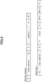
- FIG. 4 is a diagram illustrating a first example of communication data transmitted and received by the communication unit 34 according to the one embodiment. This first example illustrates communication data and communication order transmitted and received between the communication unit 34 and the MCU 40 in the case where a READ command is transmitted from the MCU 40.
- colored data represents data transmitted from the MCU 40 to the communication unit 34
- uncolored data represents data transmitted from the communication unit 34 to the MCU 40.
- the MCU 40 transmits a register address (address) of the register 32 in which data to be read is stored, to the communication unit 34, following a slave address.
- the slave address is an address specific to the IC 20.
- the MCU 40 transmits a READ command (R) to the communication unit 34 following the slave address.
- the communication unit 34 reads one item of data (Data 1) in the predetermined data unit (eight bits) from the specified address of the register 32. Then, the communication unit 34 calculates a checksum (CRC 1) by using the data (Data 1) read from the register 32, the slave address, the register address (address), and the command (R) as the calculation targets. Further, the communication unit 34 transmits the one item of data (Data 1) to the MCU 40, and then, transmits the checksum (CRC 1) to the MCU 40.
- Data 1 data in the predetermined data unit (eight bits) from the specified address of the register 32. Then, the communication unit 34 calculates a checksum (CRC 1) by using the data (Data 1) read from the register 32, the slave address, the register address (address), and the command (R) as the calculation targets. Further, the communication unit 34 transmits the one item of data (Data 1) to the MCU 40, and then, transmits the checksum (CRC 1) to the MCU 40.
- CRC 1 checksum
- FIG. 5 is a diagram illustrating a second example of communication data transmitted and received by the communication unit 34 according to the one embodiment. This second example illustrates communication data and communication order transmitted and received between the communication unit 34 and the MCU 40 in the case where a BURST READ command is transmitted from the MCU 40.
- the MCU 40 transmits a register address (address) of the register 32 in which data to be read is stored, to the communication unit 34, following a slave address.
- the MCU 40 transmits a BURST READ command (R) to the communication unit 34 following the slave address.
- the communication unit 34 reads multiple items of data (Data 1 and Data 2) each in the predetermined data unit (eight bits) from the specified address of the register 32. Then, the communication unit 34 calculates the respective checksums (CRC 1 and CRC 2) for the multiple items of data (Data 1 and Data 2) read from the register 32. At this time, for the checksum (CRC 1) of the first data (Data 1), the communication unit 34 calculates a checksum (CRC 1) by using the first data (Data 1), the slave address, the register address (address), and the command (R) as the calculation targets. Further, the communication unit 34 sequentially transmits the first data (Data 1), the checksum (CRC 1) of the first data, the second data (Data 2), and the checksum (CRC 2) of the second data to the MCU 40.
- FIG. 6 is a diagram illustrating a third example of communication data transmitted and received by the communication unit 34 according to the one embodiment. This third example illustrates communication data and communication order transmitted and received between the communication unit 34 and the MCU 40 in the case where a RESULT READ command is transmitted from the MCU 40.
- the MCU 40 transmits a register address (address) of the register 32 in which data to be read is stored, to the communication unit 34, following a slave address.
- the MCU 40 transmits a RESULT READ command (R) to the communication unit 34 following the slave address.
- the communication unit 34 reads one group of data (24 bits) including multiple items of data (Data 1, Data 2, and Data 3) each in the predetermined data unit (eight bits) from the specified address of the register 32. Then, the communication unit 34 calculates a checksum (CRC 1) by using the one group of data read from the register 32, the slave address, the register address (address), and the command (R) as the calculation targets. Further, the communication unit 34 sequentially transmits the first data (Data 1), the second data (Data 2), the third data (Data 3), and the check sum (CRC 1) of the one group of data to the MCU 40. Note that in some cases, the communication unit 34 reads a group of data (16 bits) including multiple items of data (Data 1 and Data 2) in the predetermined data unit (eight bits) from a specified address of the register 32.
- the communication unit 34 sets the initial value to "OxFF", and divides the data to be calculated (eight bits) by a generator polynomial for CRC-8 ⁇ X 8 +X 5 +X 4 +1 ⁇ , to calculate the remainder as the checksum.
- the communication unit 34 handles three types of READ commands (READ command, BURST READ command, and RESULT READ command) as targets of adding checksums.
- FIG. 7 is a diagram illustrating an example of calculation of a checksum executed by the communication unit 34 according to the one embodiment.
- FIG. 7 illustrates an example in which the communication unit 34 calculates checksums (CRC 1 and CRC 2) of first data (Data 1) and second data (Data 2) read from the register 32, in response to receiving a BURST READ command (R).
- CRC 1 and CRC 2 checksums
- the communication unit 34 calculates the checksum (CRC 1) of the first data (Data 1) in the order of the initial value, the slave address + the command (R), the register address (address), and the first data (Data 1). Note that the initial value is "OxFF", and the first data (Data 1) is "0x00". In this case, the communication unit 34 calculates "0xA2" as the checksum (CRC 1) of the first data (Data 1).
- the communication unit 34 calculates the checksum (CRC 2) of the second data (Data 2) using the initial value and the second data (Data 2). Note that the initial value is "OxFF", and the first data (Data 2) is "0x00". In this case, the communication unit 34 calculates "0xAC" as the checksum (CRC 2) of the first data (Data 2).
- the communication unit 34 includes the command obtainer 201 that obtains a command and an address transmitted from the MCU 40; the data reader 202 that reads data from the address according to the command; the checksum calculator 203 that calculates a checksum to be added to the data; and the data transmitter 204 that transmits the checksum and the data to the MCU 40, wherein the checksum calculator 203 calculates the checksum in a data unit according to the type of command.
- the communication unit 34 when transmitting to the MCU 40 data read according to a command transmitted from the MCU 40, the communication unit 34 according to the one embodiment is able to add a checksum to the data, by using a method that is more appropriate for the type of command.
- the data reader 202 reads one item of data in the predetermined data unit (eight bits) from an address, and the checksum calculator 203 calculates a checksum for the one item of data.
- the communication unit 34 when transmitting to the MCU 40 data read according to a READ command transmitted from the MCU 40, the communication unit 34 according to the one embodiment is able to add a checksum to the data, by using a method that is more appropriate for the READ command.
- the data reader 202 reads multiple items of data each in the predetermined data unit (eight bits) from an address, and the checksum calculator 203 calculates a checksum for each of the multiple items of data.
- the communication unit 34 when transmitting to the MCU 40 data read according to a BURST READ command transmitted from the MCU 40, the communication unit 34 according to the one embodiment is able to add a checksum to the data, by using a method that is more appropriate for the BURST READ command.
- the data reader 202 reads one group of data including multiple items of data each in the predetermined data unit (eight bits) from an address, and the checksum calculator 203 calculates a checksum for the one group of data.
- the communication unit 34 when transmitting to the MCU 40 data read according to a RESULT READ command transmitted from the MCU 40, the communication unit 34 according to the one embodiment is able to add a checksum to the data, by using a method that is more appropriate for the RESULT READ command.
- the checksum calculator 203 calculates a checksum for calculation targets including a command, an address, and data.
- the communication unit 34 is able to check a code error including the command, the address, and the data.
- the IC 20 described in the embodiment described above can be used as a what-is-called analog front end (AFE) for connecting a strain gauge that outputs an analog signal with a microcomputer that executes digital processing, in a load detection device that detects a load applied to an object.
- AFE analog front end
- the IC 20 may be connected to a sensor other than a strain gauge, and may be used in a system configuration other than the detection system 10 described in the above embodiment.
Landscapes
- Engineering & Computer Science (AREA)
- Theoretical Computer Science (AREA)
- Physics & Mathematics (AREA)
- General Engineering & Computer Science (AREA)
- Probability & Statistics with Applications (AREA)
- General Physics & Mathematics (AREA)
- Quality & Reliability (AREA)
- Computer Networks & Wireless Communication (AREA)
- Signal Processing (AREA)
- Computer Security & Cryptography (AREA)
- Detection And Prevention Of Errors In Transmission (AREA)
- Detection And Correction Of Errors (AREA)
- Information Transfer Systems (AREA)
- Techniques For Improving Reliability Of Storages (AREA)
- Arrangements For Transmission Of Measured Signals (AREA)
Abstract
Description
- The present invention relates to a checksum addition method, a checksum addition device, and a sensor system.
- In Non-Patent
Document 1 cited below, a technique related to an IC equipped with a temperature sensor and a humidity sensor is disclosed, that reads sensor data stored in a register in response to an external command, calculates a checksum, and transmits the sensor data and the checksum to the outside. - Non-Patent Document 1: Silicon Laboratories Inc., "I2C HUMIDITY AND TEMPERATURE SENSOR", [online], [retrieved on Mar. 30, 2020], Internet https://www.silabs.com/documents/public/data-sheets/Si7006-A20.pdf
- However, in the conventional technique, when transmitting data read in response to a command transmitted from a request source to the request source, a checksum cannot be added to the data by a method that would be more appropriate for the type of command.
- A checksum addition method according to one embodiment includes a command obtaining step of obtaining a command and an address transmitted from a request source; a data reading step of reading data from the address according to the command; a checksum calculating step of calculating a checksum to be added to the data; and a data transmitting step of transmitting the checksum and the data to the request source, wherein the checksum calculating step calculates the checksum in a data unit according to a type of the command.
- By the checksum addition method according to the one embodiment, when transmitting data read in response to a command transmitted from a request source to the request source, a checksum can be added to the data by a method that is more appropriate for the type of command.
-
-
FIG. 1 is a diagram illustrating a configuration of a detection system according to the one embodiment; -
FIG. 2 is a diagram illustrating a functional configuration of a communication unit according to the one embodiment; -
FIG. 3 is a flow chart illustrating steps of a checksum addition method executed by the communication unit according to the one embodiment; -
FIG. 4 is a diagram illustrating a first example of communication data transmitted and received by the communication unit according to the one embodiment; -
FIG. 5 is a diagram illustrating a second example of communication data transmitted and received by the communication unit according to the one embodiment; -
FIG. 6 is a diagram illustrating a third example of communication data transmitted and received by the communication unit according to the one embodiment; and -
FIG. 7 is a diagram illustrating an example of calculation of a checksum by the communication unit according to the one embodiment. - In the following, with reference to the drawings, one embodiment will be described.
-
FIG. 1 is a diagram illustrating a configuration of adetection system 10 according to the one embodiment (an example of a "sensor system"). Thedetection system 10 illustrated inFIG. 1 includes asensor 12, asensor 14, an integrated circuit (IC) 20, and a microcontroller unit (MCU) 40. - The
sensors sensors IC 20. - The
IC 20 is an integrated circuit that executes predetermined processing on sensor signals output from thesensors IC 20 can amplify a sensor signal output from thesensor register 32. - The MCU 40 is an example of a "request source" and an "external device", and by transmitting a READ command or a WRITE command to a
communication unit 34 of theIC 20 via I2C communication, can read and write information on theregister 32 of theIC 20. For example, theMCU 40 can read sensor data from theregister 32 of theIC 20 by transmitting a READ command to thecommunication unit 34, and execute predetermined digital processing using the sensor data. - As illustrated in
FIG. 1 , theIC 20 includes amultiplexer 22, a programmable gain amplifier (PGA) 24, anA-D converter 26, and adigital processing circuit 30. - The
multiplexer 22 is connected to thesensors multiplexer 22 selects either one of the sensor signals output from thesensors PGA 24. - The PGA 24 is connected to the output terminal of the
multiplexer 22. The PGA 24 is an amplifier whose gain can be changed. The PGA 24 amplifies the sensor signal output from themultiplexer 22, and outputs the amplified sensor signal to theA-D converter 26. - The
A-D converter 26 is connected to the output terminal of the PGA 24. TheA-D converter 26 converts the sensor signal output from thePGA 24 from an analog signal to a digital signal, and outputs the digital signal to thedigital processing circuit 30. - The
digital processing circuit 30 is connected to the output terminal of theA-D converter 26. Thedigital processing circuit 30 includes aregister 32 and thecommunication unit 34. Thedigital processing circuit 30 executes predetermined digital signal processing on the sensor signal (digital signal) output from theA-D converter 26. For example, thedigital processing circuit 30 stores the sensor signal (i.e., sensor data) output from theA-D converter 26 in theregister 32. Thecommunication unit 34 of thedigital processing circuit 30 reads and writes data on theregister 32 in response to a command from theMCU 40. For example, in response to a READ command transmitted from theMCU 40 via I2C communication, thecommunication unit 34 reads various items of information stored in theregister 32, and transmits the information to theMCU 40 via I2C communication. - Note that the
communication unit 34 is an example of a "checksum addition device", and has a function of adding a checksum. Thecommunication unit 34 adds a checksum (CRC (Cyclic Redundancy Check) for I2C communication) to data read from theregister 32, and transmits the data and the checksum to theMCU 40. In particular, thecommunication unit 34 according to the present embodiment can add a checksum to data by using an addition method that varies depending on the type of command. -
FIG. 2 is a diagram illustrating a functional configuration of thecommunication unit 34 according to the one embodiment. As illustrated inFIG. 2 , thecommunication unit 34 includes a command obtainer 201, adata reader 202, achecksum calculator 203, and adata transmitter 204. - The command obtainer 201 obtains a command and an address transmitted from the
MCU 40 via I2C communication with theMCU 40. - The
data reader 202 reads data from the address of theregister 32 obtained by the command obtainer 201 according to the command obtained by thecommand obtainer 201. - The
checksum calculator 203 calculates a checksum to be added to the data read by thedata reader 202. - The
data transmitter 204 transmits the data read by thedata reader 202 and the checksum calculated by thechecksum calculator 203 to theMCU 40 via I2C communication with theMCU 40. -
FIG. 3 is a flow chart illustrating steps of a checksum addition method executed by thecommunication unit 34 according to the one embodiment. - First, the command obtainer 201 obtains a command and an address transmitted from the MCU 40 (Step S301: command obtaining step).
- Next, according to the command obtained at Step S301, the
data reader 202 reads data from the address of theregister 32 obtained at Step S301 (Step S302: data reading step). - Next, the
checksum calculator 203 calculates a checksum to be added to the data read at Step S302 (Step S303: checksum calculating step). - Next, the
data transmitter 204 transmits the checksum and the date to the MCU 40 (Step S304: data transmitting step). Then, thecommunication unit 34 ends the series of steps illustrated inFIG. 3 . - Here, in the present embodiment, at the checksum calculating step of Step S303, the
checksum calculator 203 calculates a checksum in a data unit according to the type of command obtained at Step S301. - For example, in the case where the command obtained at Step S301 is a READ command (an example of a "first read command"), the
data reader 202 reads one item of data in a predetermined data unit (eight bits) from the address of theregister 32 obtained at Step S301. Then, thechecksum calculator 203 calculates the checksum for the one item of data read from theregister 32. - Also, for example, in the case where the command obtained at Step S301 is a BURST READ command (an example of a "second read command"), the
data reader 202 reads multiple items of data each in a predetermined data unit (eight bits) from the address of theregister 32 obtained at Step S301. Then, thechecksum calculator 203 calculates the checksum for each of the multiple items of data read from theregister 32. - Also, for example, in the case where the command obtained at Step S301 is a RESULT READ command (an example of a "third read command"), the
data reader 202 reads one group of data including multiple items of data each in a predetermined data unit (eight bits) from the address of theregister 32 obtained at Step S301. Then, thechecksum calculator 203 calculates the checksum for the one group of data read from theregister 32. - Further, in the present embodiment, at the checksum calculating step of Step S303, the
checksum calculator 203 calculates the checksum for calculation targets including the command obtained at Step S301, the address obtained at Step S301, and the data read at Step S302. -
FIG. 4 is a diagram illustrating a first example of communication data transmitted and received by thecommunication unit 34 according to the one embodiment. This first example illustrates communication data and communication order transmitted and received between thecommunication unit 34 and theMCU 40 in the case where a READ command is transmitted from theMCU 40. - Note that in
FIGs. 4 to 6 , colored data represents data transmitted from theMCU 40 to thecommunication unit 34, and uncolored data represents data transmitted from thecommunication unit 34 to theMCU 40. - In the first example illustrated in
FIG. 4 , first, theMCU 40 transmits a register address (address) of theregister 32 in which data to be read is stored, to thecommunication unit 34, following a slave address. Note that the slave address is an address specific to theIC 20. Next, theMCU 40 transmits a READ command (R) to thecommunication unit 34 following the slave address. - Next, in response to receiving the READ command (R), the
communication unit 34 reads one item of data (Data 1) in the predetermined data unit (eight bits) from the specified address of theregister 32. Then, thecommunication unit 34 calculates a checksum (CRC 1) by using the data (Data 1) read from theregister 32, the slave address, the register address (address), and the command (R) as the calculation targets. Further, thecommunication unit 34 transmits the one item of data (Data 1) to theMCU 40, and then, transmits the checksum (CRC 1) to theMCU 40. -
FIG. 5 is a diagram illustrating a second example of communication data transmitted and received by thecommunication unit 34 according to the one embodiment. This second example illustrates communication data and communication order transmitted and received between thecommunication unit 34 and theMCU 40 in the case where a BURST READ command is transmitted from theMCU 40. - In the second example illustrated in
FIG. 5 , first, theMCU 40 transmits a register address (address) of theregister 32 in which data to be read is stored, to thecommunication unit 34, following a slave address. Next, theMCU 40 transmits a BURST READ command (R) to thecommunication unit 34 following the slave address. - Next, in response to receiving the BURST READ command (R), the
communication unit 34 reads multiple items of data (Data 1 and Data 2) each in the predetermined data unit (eight bits) from the specified address of theregister 32. Then, thecommunication unit 34 calculates the respective checksums (CRC 1 and CRC 2) for the multiple items of data (Data 1 and Data 2) read from theregister 32. At this time, for the checksum (CRC 1) of the first data (Data 1), thecommunication unit 34 calculates a checksum (CRC 1) by using the first data (Data 1), the slave address, the register address (address), and the command (R) as the calculation targets. Further, thecommunication unit 34 sequentially transmits the first data (Data 1), the checksum (CRC 1) of the first data, the second data (Data 2), and the checksum (CRC 2) of the second data to theMCU 40. -
FIG. 6 is a diagram illustrating a third example of communication data transmitted and received by thecommunication unit 34 according to the one embodiment. This third example illustrates communication data and communication order transmitted and received between thecommunication unit 34 and theMCU 40 in the case where a RESULT READ command is transmitted from theMCU 40. - In the third example illustrated in
FIG. 6 , first, theMCU 40 transmits a register address (address) of theregister 32 in which data to be read is stored, to thecommunication unit 34, following a slave address. Next, theMCU 40 transmits a RESULT READ command (R) to thecommunication unit 34 following the slave address. - Next, in response to receiving the RESULT READ command (R), the
communication unit 34 reads one group of data (24 bits) including multiple items of data (Data 1,Data 2, and Data 3) each in the predetermined data unit (eight bits) from the specified address of theregister 32. Then, thecommunication unit 34 calculates a checksum (CRC 1) by using the one group of data read from theregister 32, the slave address, the register address (address), and the command (R) as the calculation targets. Further, thecommunication unit 34 sequentially transmits the first data (Data 1), the second data (Data 2), the third data (Data 3), and the check sum (CRC 1) of the one group of data to theMCU 40. Note that in some cases, thecommunication unit 34 reads a group of data (16 bits) including multiple items of data (Data 1 and Data 2) in the predetermined data unit (eight bits) from a specified address of theregister 32. - In the present embodiment, the
communication unit 34 sets the initial value to "OxFF", and divides the data to be calculated (eight bits) by a generator polynomial for CRC-8 {X8+X5+X4+1}, to calculate the remainder as the checksum. - Also, in the present embodiment, the
communication unit 34 handles three types of READ commands (READ command, BURST READ command, and RESULT READ command) as targets of adding checksums. -
FIG. 7 is a diagram illustrating an example of calculation of a checksum executed by thecommunication unit 34 according to the one embodiment. As one example,FIG. 7 illustrates an example in which thecommunication unit 34 calculates checksums (CRC 1 and CRC 2) of first data (Data 1) and second data (Data 2) read from theregister 32, in response to receiving a BURST READ command (R). - In the example illustrated in
FIG. 7 , thecommunication unit 34 calculates the checksum (CRC 1) of the first data (Data 1) in the order of the initial value, the slave address + the command (R), the register address (address), and the first data (Data 1). Note that the initial value is "OxFF", and the first data (Data 1) is "0x00". In this case, thecommunication unit 34 calculates "0xA2" as the checksum (CRC 1) of the first data (Data 1). - Also, in the example illustrated in
FIG. 7 , thecommunication unit 34 calculates the checksum (CRC 2) of the second data (Data 2) using the initial value and the second data (Data 2). Note that the initial value is "OxFF", and the first data (Data 2) is "0x00". In this case, thecommunication unit 34 calculates "0xAC" as the checksum (CRC 2) of the first data (Data 2). - As above, as described above, the
communication unit 34 according to the one embodiment includes thecommand obtainer 201 that obtains a command and an address transmitted from theMCU 40; thedata reader 202 that reads data from the address according to the command; thechecksum calculator 203 that calculates a checksum to be added to the data; and thedata transmitter 204 that transmits the checksum and the data to theMCU 40, wherein thechecksum calculator 203 calculates the checksum in a data unit according to the type of command. - Accordingly, when transmitting to the
MCU 40 data read according to a command transmitted from theMCU 40, thecommunication unit 34 according to the one embodiment is able to add a checksum to the data, by using a method that is more appropriate for the type of command. - Also, in the
communication unit 34 according to the one embodiment, in the case where the command obtained by thecommand obtainer 201 is a READ command, thedata reader 202 reads one item of data in the predetermined data unit (eight bits) from an address, and thechecksum calculator 203 calculates a checksum for the one item of data. - Accordingly, when transmitting to the
MCU 40 data read according to a READ command transmitted from theMCU 40, thecommunication unit 34 according to the one embodiment is able to add a checksum to the data, by using a method that is more appropriate for the READ command. - Also, in the
communication unit 34 according to the one embodiment, in the case where the command obtained by thecommand obtainer 201 is a BURST READ command, thedata reader 202 reads multiple items of data each in the predetermined data unit (eight bits) from an address, and thechecksum calculator 203 calculates a checksum for each of the multiple items of data. - Accordingly, when transmitting to the
MCU 40 data read according to a BURST READ command transmitted from theMCU 40, thecommunication unit 34 according to the one embodiment is able to add a checksum to the data, by using a method that is more appropriate for the BURST READ command. - Also, in the
communication unit 34 according to the one embodiment, in the case where the command obtained by thecommand obtainer 201 is a RESULT READ command, thedata reader 202 reads one group of data including multiple items of data each in the predetermined data unit (eight bits) from an address, and thechecksum calculator 203 calculates a checksum for the one group of data. - Accordingly, when transmitting to the
MCU 40 data read according to a RESULT READ command transmitted from theMCU 40, thecommunication unit 34 according to the one embodiment is able to add a checksum to the data, by using a method that is more appropriate for the RESULT READ command. - Also, in the
communication unit 34 according to the one embodiment, thechecksum calculator 203 calculates a checksum for calculation targets including a command, an address, and data. - Accordingly, the
communication unit 34 according to the one embodiment is able to check a code error including the command, the address, and the data. - As above, embodiments of the present invention have been described; note that the present invention is not limited to these embodiments, and various variations or modifications can be made within the scope of the gist of the present invention as set forth in the claims.
- Note that for example, the
IC 20 described in the embodiment described above can be used as a what-is-called analog front end (AFE) for connecting a strain gauge that outputs an analog signal with a microcomputer that executes digital processing, in a load detection device that detects a load applied to an object. However, it is not limited as such, and theIC 20 may be connected to a sensor other than a strain gauge, and may be used in a system configuration other than thedetection system 10 described in the above embodiment. - The present international application claims priority to
Japanese Patent Application No. 2020-070471 filed on April 9, 2020 -
- 10 detection system (sensor system)
- 12, 14 sensor
- 20 IC
- 22 multiplexer
- 24 PGA
- 26 A-D converter
- 30 digital processing circuit
- 32 register
- 34 communication unit
- 40 MCU (request source, external device)
Claims (7)
- A checksum addition method, comprising:a command obtaining step of obtaining a command and an address transmitted from a request source;a data reading step of reading data from the address according to the command;a checksum calculating step of calculating a checksum to be added to the data; anda data transmitting step of transmitting the checksum and the data to the request source,wherein the checksum calculating step calculates the checksum in a data unit according to a type of the command.
- The checksum addition method as claimed in claim 1, wherein in a case where the command obtained by the command obtaining step is a first read command, the data reading step reads one item of data in a predetermined data unit from the address, and
wherein the checksum calculating step calculates the checksum for the one item of data. - The checksum addition method as claimed in claim 1 or 2, wherein
in a case where the command obtained by the command obtaining step is a second read command, the data reading step reads multiple items of data each in a predetermined data unit from the address, and
wherein the checksum calculating step calculates the checksum for each of the multiple items of data. - The checksum addition method as claimed in any one of claims 1 to 3, wherein in a case where the command obtained by the command obtaining step is a third read command, the data reading step reads one group of data including multiple items of data each in a predetermined data unit from the address, and
wherein the checksum calculating step calculates the checksum for the one group of data. - The checksum addition method as claimed in any one of claims 1 to 4, wherein the checksum calculating step calculates the checksum for calculation targets including the command, the address, and the data.
- A checksum addition device, comprising:a command obtainer configured to obtain a command and an address transmitted from a request source;a data reader configured to read data from the address according to the command;a checksum calculator configured to calculate a checksum to be added to the data; anda data transmitter configured to transmit the checksum and the data to the request source,wherein the checksum calculator calculates the checksum in a data unit according to a type of the command.
- A sensor system comprising:a sensor;an integrated circuit configured to execute predetermined processing on an output signal of the sensor; andan external device configured to obtain necessary data from the integrated circuit,wherein the external device transmits a command from among multiple types of commands for obtaining necessary data, and an address in which the necessary data is stored, to the integrated circuit,wherein the integrated circuit includesa command obtainer configured to obtain a command and an address transmitted from a request source;a data reader configured to read data from the address according to the command;a checksum calculator configured to calculate a checksum to be added to the data; anda data transmitter configured to transmit the checksum and the data to the request source, andwherein the checksum calculator calculates the checksum in a data unit according to a type of the command.
Applications Claiming Priority (2)
| Application Number | Priority Date | Filing Date | Title |
|---|---|---|---|
| JP2020070471A JP7553041B2 (en) | 2020-04-09 | 2020-04-09 | Method and device for adding checksum |
| PCT/JP2021/013001 WO2021205910A1 (en) | 2020-04-09 | 2021-03-26 | Checksum addition method, checksum addition device, and sensor system |
Publications (3)
| Publication Number | Publication Date |
|---|---|
| EP4135204A1 true EP4135204A1 (en) | 2023-02-15 |
| EP4135204A4 EP4135204A4 (en) | 2023-06-07 |
| EP4135204B1 EP4135204B1 (en) | 2026-02-11 |
Family
ID=78023252
Family Applications (1)
| Application Number | Title | Priority Date | Filing Date |
|---|---|---|---|
| EP21784582.5A Active EP4135204B1 (en) | 2020-04-09 | 2021-03-26 | Checksum addition method, checksum addition device, and sensor system |
Country Status (5)
| Country | Link |
|---|---|
| US (1) | US12047092B2 (en) |
| EP (1) | EP4135204B1 (en) |
| JP (1) | JP7553041B2 (en) |
| CN (1) | CN115335818A (en) |
| WO (1) | WO2021205910A1 (en) |
Family Cites Families (14)
| Publication number | Priority date | Publication date | Assignee | Title |
|---|---|---|---|---|
| US4703473A (en) * | 1984-06-29 | 1987-10-27 | Hewlett-Packard Company | Serial network architecture for user oriented devices |
| US5182752A (en) * | 1990-06-29 | 1993-01-26 | Digital Equipment Corporation | Method and apparatus for transferring data between a data bus and a data storage device |
| US6467060B1 (en) * | 1998-06-26 | 2002-10-15 | Seagate Technology Llc | Mass storage error correction and detection system, method and article of manufacture |
| US6728908B1 (en) | 1999-11-18 | 2004-04-27 | California Institute Of Technology | I2C bus protocol controller with fault tolerance |
| US7647544B1 (en) * | 2005-11-22 | 2010-01-12 | Western Digital Technologies, Inc. | Disk drive implementing data path protection without writing the error detection code data to the disk |
| CN101377749B (en) * | 2007-08-31 | 2010-06-02 | 华为技术有限公司 | Memory data verification method, device, programmable logic device and system |
| US9577788B2 (en) | 2011-06-15 | 2017-02-21 | Denso Corporation | Coding apparatus, coding method, data communication apparatus, and data communication method |
| JP2013058845A (en) | 2011-09-07 | 2013-03-28 | Denso Corp | Data communication method and data communication system |
| JP6071296B2 (en) * | 2012-07-20 | 2017-02-01 | キヤノン株式会社 | Communication control device and communication control method |
| US9009566B2 (en) * | 2012-09-12 | 2015-04-14 | Macronix International Co., Ltd. | Outputting information of ECC corrected bits |
| US9569303B2 (en) * | 2014-08-08 | 2017-02-14 | Kabushiki Kaisha Toshiba | Information processing apparatus |
| US9842021B2 (en) * | 2015-08-28 | 2017-12-12 | Intel Corporation | Memory device check bit read mode |
| US11336756B2 (en) * | 2017-11-06 | 2022-05-17 | Intel Corporation | Technologies for programming flexible accelerated network pipeline using eBPF |
| JP7219051B2 (en) | 2018-10-31 | 2023-02-07 | 三菱重工業株式会社 | Acidic treatment liquid treatment apparatus and acidic treatment liquid treatment method |
-
2020
- 2020-04-09 JP JP2020070471A patent/JP7553041B2/en active Active
-
2021
- 2021-03-26 CN CN202180024523.8A patent/CN115335818A/en active Pending
- 2021-03-26 WO PCT/JP2021/013001 patent/WO2021205910A1/en not_active Ceased
- 2021-03-26 EP EP21784582.5A patent/EP4135204B1/en active Active
- 2021-03-26 US US17/906,511 patent/US12047092B2/en active Active
Also Published As
| Publication number | Publication date |
|---|---|
| WO2021205910A1 (en) | 2021-10-14 |
| JP7553041B2 (en) | 2024-09-18 |
| US20230179227A1 (en) | 2023-06-08 |
| US12047092B2 (en) | 2024-07-23 |
| JP2021168431A (en) | 2021-10-21 |
| EP4135204A4 (en) | 2023-06-07 |
| CN115335818A (en) | 2022-11-11 |
| EP4135204B1 (en) | 2026-02-11 |
Similar Documents
| Publication | Publication Date | Title |
|---|---|---|
| JPH10261185A (en) | Mixed input / output signal converter | |
| US7924202B2 (en) | Integrated circuit device and electronic instrument | |
| JP4093392B2 (en) | Self-supporting network measurement system | |
| US12047092B2 (en) | Checksum addition method, checksum addition device, and sensor system | |
| US12366588B2 (en) | Inertial measurement device and inertial measurement system | |
| CN102954814B (en) | Two-wire process control loop current diagnostic | |
| US10735830B2 (en) | Transmitter | |
| CN115950570B (en) | Pressure measurement circuit, chip and electronic equipment | |
| CN118519013A (en) | Electrical parameter testing method for four-way high-gain operational amplifier | |
| CN219244853U (en) | Pressure measurement circuit, pressure detection circuit, chip and electronic equipment | |
| EP2876970A1 (en) | Communication apparatus | |
| US20210215736A1 (en) | Method for calibrating a sensor of a device and sensor system | |
| US20190354271A1 (en) | Transducer programmer | |
| JP2541438B2 (en) | Signal input circuit | |
| CN111141314A (en) | Sensor interface circuit | |
| AU2019203833B2 (en) | Weighing instrument using a general-purpose computer as the primary display and data entry | |
| RU2546576C2 (en) | 4-20mA TRANSCEIVER | |
| KR102597358B1 (en) | Apparatus and method for testing analog signal of industrial inverter | |
| CN113330686A (en) | Transmission of values by means of pulse-width-modulated signals | |
| CN118129957A (en) | Pressure detection circuit, pressure detection method, computer device, and storage medium | |
| JPS6395597A (en) | Measurement data transmission method | |
| TWM591271U (en) | Integrate multiple sensor systems with a single MCU | |
| JP2007333453A (en) | Encoder temperature measurement method and encoder | |
| JPS61123230A (en) | Terminal device for transmission system | |
| JP2004198309A (en) | Temperature output method of encoder with temperature sensor |
Legal Events
| Date | Code | Title | Description |
|---|---|---|---|
| STAA | Information on the status of an ep patent application or granted ep patent |
Free format text: STATUS: THE INTERNATIONAL PUBLICATION HAS BEEN MADE |
|
| PUAI | Public reference made under article 153(3) epc to a published international application that has entered the european phase |
Free format text: ORIGINAL CODE: 0009012 |
|
| STAA | Information on the status of an ep patent application or granted ep patent |
Free format text: STATUS: REQUEST FOR EXAMINATION WAS MADE |
|
| 17P | Request for examination filed |
Effective date: 20220923 |
|
| AK | Designated contracting states |
Kind code of ref document: A1 Designated state(s): AL AT BE BG CH CY CZ DE DK EE ES FI FR GB GR HR HU IE IS IT LI LT LU LV MC MK MT NL NO PL PT RO RS SE SI SK SM TR |
|
| A4 | Supplementary search report drawn up and despatched |
Effective date: 20230511 |
|
| RIC1 | Information provided on ipc code assigned before grant |
Ipc: G06F 13/42 20060101ALI20230504BHEP Ipc: G06F 13/38 20060101ALI20230504BHEP Ipc: G06F 11/10 20060101ALI20230504BHEP Ipc: H04L 1/00 20060101ALI20230504BHEP Ipc: H03M 13/35 20060101ALI20230504BHEP Ipc: H03M 13/09 20060101AFI20230504BHEP |
|
| DAV | Request for validation of the european patent (deleted) | ||
| DAX | Request for extension of the european patent (deleted) | ||
| STAA | Information on the status of an ep patent application or granted ep patent |
Free format text: STATUS: EXAMINATION IS IN PROGRESS |
|
| 17Q | First examination report despatched |
Effective date: 20250429 |
|
| GRAP | Despatch of communication of intention to grant a patent |
Free format text: ORIGINAL CODE: EPIDOSNIGR1 |
|
| STAA | Information on the status of an ep patent application or granted ep patent |
Free format text: STATUS: GRANT OF PATENT IS INTENDED |
|
| INTG | Intention to grant announced |
Effective date: 20251015 |
|
| GRAS | Grant fee paid |
Free format text: ORIGINAL CODE: EPIDOSNIGR3 |
|
| GRAA | (expected) grant |
Free format text: ORIGINAL CODE: 0009210 |
|
| STAA | Information on the status of an ep patent application or granted ep patent |
Free format text: STATUS: THE PATENT HAS BEEN GRANTED |
|
| AK | Designated contracting states |
Kind code of ref document: B1 Designated state(s): AL AT BE BG CH CY CZ DE DK EE ES FI FR GB GR HR HU IE IS IT LI LT LU LV MC MK MT NL NO PL PT RO RS SE SI SK SM TR |
|
| REG | Reference to a national code |
Ref country code: CH Ref legal event code: F10 Free format text: ST27 STATUS EVENT CODE: U-0-0-F10-F00 (AS PROVIDED BY THE NATIONAL OFFICE) Effective date: 20260211 Ref country code: GB Ref legal event code: FG4D |
|
| REG | Reference to a national code |
Ref country code: DE Ref legal event code: R096 Ref document number: 602021047780 Country of ref document: DE |
|
| REG | Reference to a national code |
Ref country code: IE Ref legal event code: FG4D |
|
| PGFP | Annual fee paid to national office [announced via postgrant information from national office to epo] |
Ref country code: DE Payment date: 20260319 Year of fee payment: 6 |
|
| P01 | Opt-out of the competence of the unified patent court (upc) registered |
Free format text: CASE NUMBER: UPC_APP_0010254_4135204/2026 Effective date: 20260318 |