EP4135135B1 - Photonic crystal surface-emitting laser - Google Patents
Photonic crystal surface-emitting laser Download PDFInfo
- Publication number
- EP4135135B1 EP4135135B1 EP21198917.3A EP21198917A EP4135135B1 EP 4135135 B1 EP4135135 B1 EP 4135135B1 EP 21198917 A EP21198917 A EP 21198917A EP 4135135 B1 EP4135135 B1 EP 4135135B1
- Authority
- EP
- European Patent Office
- Prior art keywords
- photonic crystal
- layer
- active layer
- emitting laser
- type cladding
- Prior art date
- Legal status (The legal status is an assumption and is not a legal conclusion. Google has not performed a legal analysis and makes no representation as to the accuracy of the status listed.)
- Active
Links
Images





Classifications
-
- H—ELECTRICITY
- H01—ELECTRIC ELEMENTS
- H01S—DEVICES USING THE PROCESS OF LIGHT AMPLIFICATION BY STIMULATED EMISSION OF RADIATION [LASER] TO AMPLIFY OR GENERATE LIGHT; DEVICES USING STIMULATED EMISSION OF ELECTROMAGNETIC RADIATION IN WAVE RANGES OTHER THAN OPTICAL
- H01S5/00—Semiconductor lasers
- H01S5/10—Construction or shape of the optical resonator, e.g. extended or external cavity, coupled cavities, bent-guide, varying width, thickness or composition of the active region
- H01S5/18—Surface-emitting [SE] lasers, e.g. having both horizontal and vertical cavities
- H01S5/183—Surface-emitting [SE] lasers, e.g. having both horizontal and vertical cavities having only vertical cavities, e.g. vertical cavity surface-emitting lasers [VCSEL]
- H01S5/18308—Surface-emitting [SE] lasers, e.g. having both horizontal and vertical cavities having only vertical cavities, e.g. vertical cavity surface-emitting lasers [VCSEL] having a special structure for lateral current or light confinement
- H01S5/18322—Position of the structure
-
- H—ELECTRICITY
- H01—ELECTRIC ELEMENTS
- H01S—DEVICES USING THE PROCESS OF LIGHT AMPLIFICATION BY STIMULATED EMISSION OF RADIATION [LASER] TO AMPLIFY OR GENERATE LIGHT; DEVICES USING STIMULATED EMISSION OF ELECTROMAGNETIC RADIATION IN WAVE RANGES OTHER THAN OPTICAL
- H01S5/00—Semiconductor lasers
- H01S5/10—Construction or shape of the optical resonator, e.g. extended or external cavity, coupled cavities, bent-guide, varying width, thickness or composition of the active region
- H01S5/11—Comprising a photonic bandgap structure
-
- H—ELECTRICITY
- H01—ELECTRIC ELEMENTS
- H01S—DEVICES USING THE PROCESS OF LIGHT AMPLIFICATION BY STIMULATED EMISSION OF RADIATION [LASER] TO AMPLIFY OR GENERATE LIGHT; DEVICES USING STIMULATED EMISSION OF ELECTROMAGNETIC RADIATION IN WAVE RANGES OTHER THAN OPTICAL
- H01S5/00—Semiconductor lasers
- H01S5/04—Processes or apparatus for excitation, e.g. pumping, e.g. by electron beams
- H01S5/042—Electrical excitation ; Circuits therefor
- H01S5/0425—Electrodes, e.g. characterised by the structure
- H01S5/04256—Electrodes, e.g. characterised by the structure characterised by the configuration
-
- H—ELECTRICITY
- H01—ELECTRIC ELEMENTS
- H01S—DEVICES USING THE PROCESS OF LIGHT AMPLIFICATION BY STIMULATED EMISSION OF RADIATION [LASER] TO AMPLIFY OR GENERATE LIGHT; DEVICES USING STIMULATED EMISSION OF ELECTROMAGNETIC RADIATION IN WAVE RANGES OTHER THAN OPTICAL
- H01S5/00—Semiconductor lasers
- H01S5/10—Construction or shape of the optical resonator, e.g. extended or external cavity, coupled cavities, bent-guide, varying width, thickness or composition of the active region
- H01S5/18—Surface-emitting [SE] lasers, e.g. having both horizontal and vertical cavities
- H01S5/183—Surface-emitting [SE] lasers, e.g. having both horizontal and vertical cavities having only vertical cavities, e.g. vertical cavity surface-emitting lasers [VCSEL]
- H01S5/18361—Structure of the reflectors, e.g. hybrid mirrors
- H01S5/18377—Structure of the reflectors, e.g. hybrid mirrors comprising layers of different kind of materials, e.g. combinations of semiconducting with dielectric or metallic layers
-
- H—ELECTRICITY
- H01—ELECTRIC ELEMENTS
- H01S—DEVICES USING THE PROCESS OF LIGHT AMPLIFICATION BY STIMULATED EMISSION OF RADIATION [LASER] TO AMPLIFY OR GENERATE LIGHT; DEVICES USING STIMULATED EMISSION OF ELECTROMAGNETIC RADIATION IN WAVE RANGES OTHER THAN OPTICAL
- H01S5/00—Semiconductor lasers
- H01S5/10—Construction or shape of the optical resonator, e.g. extended or external cavity, coupled cavities, bent-guide, varying width, thickness or composition of the active region
- H01S5/18—Surface-emitting [SE] lasers, e.g. having both horizontal and vertical cavities
- H01S5/185—Surface-emitting [SE] lasers, e.g. having both horizontal and vertical cavities having only horizontal cavities, e.g. horizontal cavity surface-emitting lasers [HCSEL]
-
- H—ELECTRICITY
- H01—ELECTRIC ELEMENTS
- H01S—DEVICES USING THE PROCESS OF LIGHT AMPLIFICATION BY STIMULATED EMISSION OF RADIATION [LASER] TO AMPLIFY OR GENERATE LIGHT; DEVICES USING STIMULATED EMISSION OF ELECTROMAGNETIC RADIATION IN WAVE RANGES OTHER THAN OPTICAL
- H01S5/00—Semiconductor lasers
- H01S5/20—Structure or shape of the semiconductor body to guide the optical wave ; Confining structures perpendicular to the optical axis, e.g. index or gain guiding, stripe geometry, broad area lasers, gain tailoring, transverse or lateral reflectors, special cladding structures, MQW barrier reflection layers
- H01S5/22—Structure or shape of the semiconductor body to guide the optical wave ; Confining structures perpendicular to the optical axis, e.g. index or gain guiding, stripe geometry, broad area lasers, gain tailoring, transverse or lateral reflectors, special cladding structures, MQW barrier reflection layers having a ridge or stripe structure
- H01S5/227—Buried mesa structure ; Striped active layer
-
- H—ELECTRICITY
- H01—ELECTRIC ELEMENTS
- H01S—DEVICES USING THE PROCESS OF LIGHT AMPLIFICATION BY STIMULATED EMISSION OF RADIATION [LASER] TO AMPLIFY OR GENERATE LIGHT; DEVICES USING STIMULATED EMISSION OF ELECTROMAGNETIC RADIATION IN WAVE RANGES OTHER THAN OPTICAL
- H01S5/00—Semiconductor lasers
- H01S5/30—Structure or shape of the active region; Materials used for the active region
- H01S5/34—Structure or shape of the active region; Materials used for the active region comprising quantum well or superlattice structures, e.g. single quantum well [SQW] lasers, multiple quantum well [MQW] lasers or graded index separate confinement heterostructure [GRINSCH] lasers
- H01S5/343—Structure or shape of the active region; Materials used for the active region comprising quantum well or superlattice structures, e.g. single quantum well [SQW] lasers, multiple quantum well [MQW] lasers or graded index separate confinement heterostructure [GRINSCH] lasers in AIIIBV compounds, e.g. AlGaAs-laser, InP-based laser
-
- H—ELECTRICITY
- H01—ELECTRIC ELEMENTS
- H01S—DEVICES USING THE PROCESS OF LIGHT AMPLIFICATION BY STIMULATED EMISSION OF RADIATION [LASER] TO AMPLIFY OR GENERATE LIGHT; DEVICES USING STIMULATED EMISSION OF ELECTROMAGNETIC RADIATION IN WAVE RANGES OTHER THAN OPTICAL
- H01S2301/00—Functional characteristics
- H01S2301/18—Semiconductor lasers with special structural design for influencing the near- or far-field
-
- H—ELECTRICITY
- H01—ELECTRIC ELEMENTS
- H01S—DEVICES USING THE PROCESS OF LIGHT AMPLIFICATION BY STIMULATED EMISSION OF RADIATION [LASER] TO AMPLIFY OR GENERATE LIGHT; DEVICES USING STIMULATED EMISSION OF ELECTROMAGNETIC RADIATION IN WAVE RANGES OTHER THAN OPTICAL
- H01S5/00—Semiconductor lasers
- H01S5/04—Processes or apparatus for excitation, e.g. pumping, e.g. by electron beams
- H01S5/042—Electrical excitation ; Circuits therefor
- H01S5/0425—Electrodes, e.g. characterised by the structure
- H01S5/04252—Electrodes, e.g. characterised by the structure characterised by the material
- H01S5/04253—Electrodes, e.g. characterised by the structure characterised by the material having specific optical properties, e.g. transparent electrodes
-
- H—ELECTRICITY
- H01—ELECTRIC ELEMENTS
- H01S—DEVICES USING THE PROCESS OF LIGHT AMPLIFICATION BY STIMULATED EMISSION OF RADIATION [LASER] TO AMPLIFY OR GENERATE LIGHT; DEVICES USING STIMULATED EMISSION OF ELECTROMAGNETIC RADIATION IN WAVE RANGES OTHER THAN OPTICAL
- H01S5/00—Semiconductor lasers
- H01S5/04—Processes or apparatus for excitation, e.g. pumping, e.g. by electron beams
- H01S5/042—Electrical excitation ; Circuits therefor
- H01S5/0425—Electrodes, e.g. characterised by the structure
- H01S5/04254—Electrodes, e.g. characterised by the structure characterised by the shape
-
- H—ELECTRICITY
- H01—ELECTRIC ELEMENTS
- H01S—DEVICES USING THE PROCESS OF LIGHT AMPLIFICATION BY STIMULATED EMISSION OF RADIATION [LASER] TO AMPLIFY OR GENERATE LIGHT; DEVICES USING STIMULATED EMISSION OF ELECTROMAGNETIC RADIATION IN WAVE RANGES OTHER THAN OPTICAL
- H01S5/00—Semiconductor lasers
- H01S5/20—Structure or shape of the semiconductor body to guide the optical wave ; Confining structures perpendicular to the optical axis, e.g. index or gain guiding, stripe geometry, broad area lasers, gain tailoring, transverse or lateral reflectors, special cladding structures, MQW barrier reflection layers
- H01S5/2004—Confining in the direction perpendicular to the layer structure
- H01S5/2009—Confining in the direction perpendicular to the layer structure by using electron barrier layers
-
- H—ELECTRICITY
- H01—ELECTRIC ELEMENTS
- H01S—DEVICES USING THE PROCESS OF LIGHT AMPLIFICATION BY STIMULATED EMISSION OF RADIATION [LASER] TO AMPLIFY OR GENERATE LIGHT; DEVICES USING STIMULATED EMISSION OF ELECTROMAGNETIC RADIATION IN WAVE RANGES OTHER THAN OPTICAL
- H01S5/00—Semiconductor lasers
- H01S5/20—Structure or shape of the semiconductor body to guide the optical wave ; Confining structures perpendicular to the optical axis, e.g. index or gain guiding, stripe geometry, broad area lasers, gain tailoring, transverse or lateral reflectors, special cladding structures, MQW barrier reflection layers
- H01S5/2054—Methods of obtaining the confinement
- H01S5/2059—Methods of obtaining the confinement by means of particular conductivity zones, e.g. obtained by particle bombardment or diffusion
- H01S5/2072—Methods of obtaining the confinement by means of particular conductivity zones, e.g. obtained by particle bombardment or diffusion obtained by vacancy induced diffusion
-
- H—ELECTRICITY
- H01—ELECTRIC ELEMENTS
- H01S—DEVICES USING THE PROCESS OF LIGHT AMPLIFICATION BY STIMULATED EMISSION OF RADIATION [LASER] TO AMPLIFY OR GENERATE LIGHT; DEVICES USING STIMULATED EMISSION OF ELECTROMAGNETIC RADIATION IN WAVE RANGES OTHER THAN OPTICAL
- H01S5/00—Semiconductor lasers
- H01S5/20—Structure or shape of the semiconductor body to guide the optical wave ; Confining structures perpendicular to the optical axis, e.g. index or gain guiding, stripe geometry, broad area lasers, gain tailoring, transverse or lateral reflectors, special cladding structures, MQW barrier reflection layers
- H01S5/22—Structure or shape of the semiconductor body to guide the optical wave ; Confining structures perpendicular to the optical axis, e.g. index or gain guiding, stripe geometry, broad area lasers, gain tailoring, transverse or lateral reflectors, special cladding structures, MQW barrier reflection layers having a ridge or stripe structure
- H01S5/2205—Structure or shape of the semiconductor body to guide the optical wave ; Confining structures perpendicular to the optical axis, e.g. index or gain guiding, stripe geometry, broad area lasers, gain tailoring, transverse or lateral reflectors, special cladding structures, MQW barrier reflection layers having a ridge or stripe structure comprising special burying or current confinement layers
- H01S5/2218—Structure or shape of the semiconductor body to guide the optical wave ; Confining structures perpendicular to the optical axis, e.g. index or gain guiding, stripe geometry, broad area lasers, gain tailoring, transverse or lateral reflectors, special cladding structures, MQW barrier reflection layers having a ridge or stripe structure comprising special burying or current confinement layers having special optical properties
-
- H—ELECTRICITY
- H01—ELECTRIC ELEMENTS
- H01S—DEVICES USING THE PROCESS OF LIGHT AMPLIFICATION BY STIMULATED EMISSION OF RADIATION [LASER] TO AMPLIFY OR GENERATE LIGHT; DEVICES USING STIMULATED EMISSION OF ELECTROMAGNETIC RADIATION IN WAVE RANGES OTHER THAN OPTICAL
- H01S5/00—Semiconductor lasers
- H01S5/20—Structure or shape of the semiconductor body to guide the optical wave ; Confining structures perpendicular to the optical axis, e.g. index or gain guiding, stripe geometry, broad area lasers, gain tailoring, transverse or lateral reflectors, special cladding structures, MQW barrier reflection layers
- H01S5/22—Structure or shape of the semiconductor body to guide the optical wave ; Confining structures perpendicular to the optical axis, e.g. index or gain guiding, stripe geometry, broad area lasers, gain tailoring, transverse or lateral reflectors, special cladding structures, MQW barrier reflection layers having a ridge or stripe structure
- H01S5/2205—Structure or shape of the semiconductor body to guide the optical wave ; Confining structures perpendicular to the optical axis, e.g. index or gain guiding, stripe geometry, broad area lasers, gain tailoring, transverse or lateral reflectors, special cladding structures, MQW barrier reflection layers having a ridge or stripe structure comprising special burying or current confinement layers
- H01S5/2222—Structure or shape of the semiconductor body to guide the optical wave ; Confining structures perpendicular to the optical axis, e.g. index or gain guiding, stripe geometry, broad area lasers, gain tailoring, transverse or lateral reflectors, special cladding structures, MQW barrier reflection layers having a ridge or stripe structure comprising special burying or current confinement layers having special electric properties
- H01S5/2224—Structure or shape of the semiconductor body to guide the optical wave ; Confining structures perpendicular to the optical axis, e.g. index or gain guiding, stripe geometry, broad area lasers, gain tailoring, transverse or lateral reflectors, special cladding structures, MQW barrier reflection layers having a ridge or stripe structure comprising special burying or current confinement layers having special electric properties semi-insulating semiconductors
Definitions
- the present disclosure relates to a photonic crystal surface-emitting laser.
- Lasers are widely used in different fields such as medicine, optical communication and industrial processing.
- convention lasers have drawbacks such as large divergence angle and large threshold current. This problem remains to be solved.
- US 10,340,659 B1 and US 2019/013647 A1 disclose such conventional prior art lasers, especially photonic crystal surface-emitting lasers having a first substrate, a cladding layer disposed over the first substrate, an active layer disposed over the cladding layer, and a photonic crystal structure disposed over the active layer.
- US 2007/201526 A1 discloses a vertical cavity surface emitting laser, having a cavity formed by pair of two-dimensional photonic crystal reflectors, with an active layer interposed in the cavity, and wherein the active layer is surrounded laterally by a current-confining structure.
- one of the objects of the present disclosure is to provide a photonic crystal surface-emitting laser with small divergence angle and small threshold current.
- the invention provides for a photonic crystal surface-emitting laser according to claim 1.
- the laser according to the invention includes a first substrate, an n-type cladding layer, an active layer, an index matching layer and a photonic crystal structure.
- the n-type cladding layer is disposed over the first substrate.
- the active layer is disposed over the n-type cladding layer.
- the index matching layer is disposed over the n-type cladding layer and is arranged around the active layer.
- the index matching layer is electrically insulating, and an effective refractive index of the index matching layer is substantially identical to an effective refractive index of the active layer.
- the photonic crystal structure is disposed over the active layer and the index matching layer.
- the index matching layer is transparent to light emitted by the active layer.
- a lateral length of the active layer is smaller than a lateral length of the photonic crystal structure.
- the active layer is located in an orthogonal projection area of the photonic crystal structure onto the n-type cladding layer.
- the index matching layer is at least partially located in an orthogonal projection area of the photonic crystal structure onto the n-type cladding layer, and the index matching layer is in contact with a side surface of the active layer.
- a cross-sectional area of the active layer is smaller than a cross-sectional area of the photonic crystal structure.
- a lateral length of the active layer is within a range from 6 to 10 micrometers.
- the active layer further has a top surface and a bottom surface.
- the top surface faces the photonic crystal structure.
- the bottom surface faces the n-type cladding layer.
- the side surface is connected between the top surface and the bottom surface.
- the index matching layer is spaced apart from the top surface and the bottom surface of the active layer.
- the active layer is cylindrical.
- the photonic crystal surface-emitting laser further includes an electron blocking layer disposed over the active layer and the index matching layer.
- the photonic crystal surface-emitting laser further includes a p-type cladding layer and a second substrate.
- the p-type cladding layer is disposed over the photonic crystal structure.
- the second substrate is disposed over the p-type cladding layer.
- the photonic crystal surface-emitting laser further includes a metal electrode.
- the metal electrode is disposed on a side of the second substrate away from the p-type cladding layer, and the metal electrode is in contact with a surface of the second substrate away from the p-type cladding layer.
- the photonic crystal surface-emitting laser further includes a transparent conductive layer disposed over the photonic crystal structure.
- the photonic crystal surface-emitting laser further includes a metal electrode.
- the metal electrode is disposed on a side of the transparent conductive layer away from the photonic crystal structure, and the metal electrode is in contact with a surface of the transparent conductive layer away from the photonic crystal structure.
- the photonic crystal surface-emitting laser further includes a metal electrode.
- the metal electrode is disposed on a side of the first substrate away from the n-type cladding layer, and the metal electrode is in contact with a surface of the first substrate away from the n-type cladding layer.
- the photonic crystal structure includes a plurality of periodic holes.
- the first substrate, the n-type cladding layer and the active layer are arranged along a direction, and the periodic holes are arranged on a plane normal to the direction.
- the periodic holes have circular, quadrangular or hexagonal cross-sections.
- the active layer includes quantum well.
- the photonic crystal surface-emitting laser of the present disclosure includes an index matching layer arranged around the active layer.
- the index matching layer is electrically insulating, and an effective refractive index of the index matching layer is substantially identical to an effective refractive index of the active layer.
- the photonic crystal surface-emitting laser of the present disclosure can have smaller divergence angle and smaller threshold current.
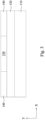
- Fig. 1A illustrates a top view of a photonic crystal surface-emitting laser 100 in accordance with an embodiment of the present disclosure.
- Fig. 1B illustrates an enlarged perspective view of the photonic crystal surface-emitting laser 100 shown in Fig. 1A in the area M.
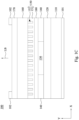
- Fig. 1C illustrates a sectional view of the photonic crystal surface-emitting laser 100 shown in Fig. 1A taken along line segment 1-1'.
- the photonic crystal surface-emitting laser 100 includes a first substrate 110, an n-type cladding layer 120, an active layer 130, an index matching layer 140, a photonic crystal structure 150, a p-type cladding layer 160, and a second substrate 170 in a stack arrangement along a first direction Y.
- the first substrate 110 is, for example, a semiconductor substrate, which may include GaAs or other suitable semiconductor material.
- the n-type cladding layer 120 is disposed over the first substrate 110.
- the active layer 130 and the index matching layer 140 are disposed over the n-type cladding layer 120.
- the active layer 130 includes quantum well and is configured to emit light when a voltage is applied to the photonic crystal surface-emitting laser 100.
- the n-type cladding layer 120 may include GaAs, InGaAs, InGaAsP, AlAs, AlGaInAs, AlGaInP, AlGaAs, InGaNAs, GaAsSb, GaSb, InP, InAs, GaP, AlP, GaN, AlGaN, InGaN, AlInGaN, other suitable semiconductor material, or any combination thereof.
- the photonic crystal structure 150 is disposed over the active layer 130 and the index matching layer 140.
- the light emitted by the active layer 130 can resonate in the photonic crystal structure 150 and thereby produce a laser beam LB.
- the laser beam LB is output from the top of the photonic crystal surface-emitting laser 100 along the first direction Y.
- the photonic crystal structure 150 includes a base portion 151 and a plurality of periodic holes 152.
- the base portion 151 may include GaAs or other suitable semiconductor material.
- the periodic holes 152 are formed on a side of the base portion 151 that is away from the active layer 130 and the index matching layer 140.
- the periodic holes 152 are arranged in a second direction X substantially normal to the first direction Y.
- the periodic holes 152 are arranged on a plane normal to the first direction Y.
- the periodic holes 152 have circular, quadrangular or hexagonal cross-sections.
- the p-type cladding layer 160 is disposed over the photonic crystal structure 150, and the second substrate 170 is disposed over the p-type cladding layer 160.
- the second substrate 170 may include p-type semiconductor material such as p-GaAs.
- the p-type cladding layer 160 may include GaAs, InGaAs, InGaAsP, AlAs, AlGaInAs, AlGaInP, AlGaAs, InGaNAs, GaAsSb, GaSb, InP, InAs, GaP, AlP, GaN, AlGaN, InGaN, AlInGaN, other suitable semiconductor material, or any combination thereof.
- the index matching layer 140 is arranged around the active layer 130.
- the active layer 130 is cylindrical.
- the active layer 130 takes the shape of a circular disk in top view.
- the index matching layer 140 is spaced apart from a bottom surface of the active layer 130 (i.e., the surface of the active layer 130 facing the n-type cladding layer 120) and a top surface of the active layer 130 (i.e., the surface of the active layer 130 facing the photonic crystal structure 150), and is in contact with a side surface of the active layer 130 (i.e., the surface of the active layer 130 connected between the top surface and the bottom surface).
- the index matching layer 140 is electrically insulating, such that electric current only passes through the active layer 130 when a voltage is applied to the photonic crystal surface-emitting laser 100.
- the index matching layer 140 does not emit light and does not absorb light.
- an effective refractive index of the index matching layer 140 is substantially identical to an effective refractive index of the active layer 130.
- the index matching layer 140 includes dielectric material. In some embodiments, the index matching layer 140 includes non-conductive or high-impedance semiconductor material (e.g., undoped semiconductor material, or doped semiconductor material such as GaN doped with Fe). The index matching layer 140 is transparent to the light emitted by the active layer 130.
- non-conductive or high-impedance semiconductor material e.g., undoped semiconductor material, or doped semiconductor material such as GaN doped with Fe.
- a cross-sectional area of the active layer 130 (specifically, the area of the cross-section of the active layer 130 that is normal to the first direction Y) is smaller than a cross-sectional area of the photonic crystal structure 150 (specifically, the area of the cross-section of the photonic crystal structure 150 that is normal to the first direction Y).
- a voltage is applied to the photonic crystal surface-emitting laser 100, the electric current passes through the active layer 130 of smaller size, but laser can be emitted from the photonic crystal structure 150 of greater size, resulting in an enlarged emission area.
- a ratio of the cross-sectional area of the index matching layer 140 to the cross-sectional area of the active layer 130 is within a range from 1.5 to 100.
- a lateral length W1 of the active layer 130 is smaller than a lateral length W2 of the photonic crystal structure 150, in which "lateral length” refers to the length in the second direction X.
- the lateral length W1 of the active layer 130 is within a range from 6 to 10 micrometers. In the embodiments where the active layer 130 is cylindrical, the lateral length W1 is equivalent to the diameter of the active layer 130.
- the active layer 130 is located in an orthogonal projection area of the photonic crystal structure 150 onto the n-type cladding layer 120, in which "orthogonal projection area” refers to the area of projection along the opposite direction of the first direction Y.
- the index matching layer 140 is at least partially located in the orthogonal projection area of the photonic crystal structure 150 onto the n-type cladding layer 120.
- the photonic crystal surface-emitting laser 100 further includes an electron blocking layer 180 covering the active layer 130 and the index matching layer 140.
- the electron blocking layer 180 is disposed between the photonic crystal structure 150 and the active layer 130/the index matching layer 140.
- the photonic crystal surface-emitting laser 100 further includes a first electrode 101 and a second electrode 102.
- the first electrode 101 is disposed on a side of the first substrate 110 away from the n-type cladding layer 120, and the first electrode 101 is in contact with a surface of the first substrate 110 away from the n-type cladding layer 120.
- the second electrode 102 is disposed on a side of the second substrate 170 away from the p-type cladding layer 160, and the second electrode 102 is in contact with a surface of the second substrate 170 away from the p-type cladding layer 160.
- the first and second electrodes 101 and 102 are metal electrodes.
- the second electrode 102 includes a ring structure. The ring structure has a central opening configured to allow the laser beam LB to pass through.
- the first and second electrodes 101 and 102 may include In, Sn, Al, Au, Pt, Zn, Ge, Ag, Pb, Pd, Cu, AuBe, BeGe, Ni, PbSn, Cr,
- a method for manufacturing the photonic crystal surface-emitting laser 100 will be described below with reference to Figs. 2 to 6 .
- Figs. 2 to 6 illustrate sectional views of the photonic crystal surface-emitting laser 100 of Fig. 1C at various stages of manufacturing.
- the method for manufacturing the photonic crystal surface-emitting laser 100 includes step S1 to S11.
- step S1 includes forming the first substrate 110, the n-type cladding layer 120 and the active layer 130.
- the first substrate 110, the n-type cladding layer 120 and the active layer 130 are in a stack arrangement along the first direction Y.
- the active layer 130 covers a top surface of the n-type cladding layer 120.
- step S1 includes forming the first substrate 110, the n-type cladding layer 120 and the active layer 130 by means of epitaxial growth.
- step S3 includes forming the index matching layer 140 around the active layer 130.
- step S3 includes etching the peripheral region of the active layer 130 formed in step S1 and then forming the index matching layer 140 around the active layer 130 by means of epitaxial growth.
- step S3 includes carrying out a quantum well intermixing process to the active layer 130 to form the index matching layer 140.
- step S5 includes forming the electron blocking layer 180 and a semiconductor layer 150A (e.g., p-GaAs) over the active layer 130 and the index matching layer 140.
- the electron blocking layer 180 and the semiconductor layer 150A are in a stack arrangement along the first direction Y.
- the semiconductor layer 150A covers a top surface of the electron blocking layer 180.
- step S5 includes forming the electron blocking layer 180 and the semiconductor layer 150A over the active layer 130 and the index matching layer 140 by means of epitaxial growth.
- step S7 includes forming the photonic crystal structure 150 in the semiconductor layer 150A.
- step S7 includes removing part of the semiconductor layer 150A to form the periodic holes 152 of the photonic crystal structure 150. The remaining part of the semiconductor layer 150A becomes the base portion 151 of the photonic crystal structure 150.
- step S7 includes removing part of the semiconductor layer 150A to form the periodic holes 152 of the photonic crystal structure 150 by means of etching or lithography.
- step S9 includes forming the p-type cladding layer 160 and the second substrate 170 (e.g., p-GaAs) over the photonic crystal structure 150.
- the p-type cladding layer 160 and the second substrate 170 are in a stack arrangement along the first direction Y.
- the second substrate 170 covers a top surface of the p-type cladding layer 160.
- step S9 includes forming the p-type cladding layer 160 and the second substrate 170 over the photonic crystal structure 150 by means of epitaxial growth.
- the method for manufacturing the photonic crystal surface-emitting laser 100 concludes at step S11, which includes forming the first and second electrodes 101 and 102.
- the first electrode 101 is disposed on the side of the first substrate 110 away from the n-type cladding layer 120, and the first electrode 101 is in contact with the surface of the first substrate 110 away from the n-type cladding layer 120.
- the second electrode 102 is disposed on the side of the second substrate 170 away from the p-type cladding layer 160, and the second electrode 102 is in contact with the surface of the second substrate 170 away from the p-type cladding layer 160.
- step S11 includes depositing the first electrode 101 on the surface of the first substrate 110 away from the n-type cladding layer 120, and depositing the second electrode 102 on the surface of the second substrate 170 away from the p-type cladding layer 160.
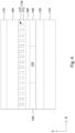
- the photonic crystal surface-emitting laser 200 of the present embodiment includes a transparent conductive layer 290 to replace the p-type cladding layer 160 and the second substrate 170.
- the transparent conductive layer 290 covers a side of the photonic crystal structure 150 away from the active layer 130.
- the second electrode 102 is disposed over the transparent conductive layer 290, and the second electrode 102 is in contact with a surface of the transparent conductive layer 290 away from the photonic crystal structure 150.
- a method for manufacturing the photonic crystal surface-emitting laser 200 includes: after forming the photonic crystal structure 150, coating the transparent conductive layer 290 on the side of the photonic crystal structure 150 away from the active layer 130.
- the transparent conductive layer 290 includes ITO, ZnO, AlGaInSnO, AZO, SnO 2 , In 2 O 3 , SnZnO, graphene, other suitable electrically conductive material, or any combination thereof. These materials have decent transmissivity in the visible spectrum and the infrared region, and can thus facilitate the output of the light beam LB.
- the photonic crystal surface-emitting laser of the present disclosure includes an index matching layer arranged around the active layer.
- the index matching layer is electrically insulating, and an effective refractive index of the index matching layer is substantially identical to an effective refractive index of the active layer.
- the photonic crystal surface-emitting laser of the present disclosure can have smaller divergence angle and smaller threshold current.
Landscapes
- Physics & Mathematics (AREA)
- Condensed Matter Physics & Semiconductors (AREA)
- General Physics & Mathematics (AREA)
- Electromagnetism (AREA)
- Optics & Photonics (AREA)
- Geometry (AREA)
- Semiconductor Lasers (AREA)
- Lasers (AREA)
Description
- The present disclosure relates to a photonic crystal surface-emitting laser.
- Lasers are widely used in different fields such as medicine, optical communication and industrial processing. However, convention lasers have drawbacks such as large divergence angle and large threshold current. This problem remains to be solved.
-
US 10,340,659 B1 US 2019/013647 A1 disclose such conventional prior art lasers, especially photonic crystal surface-emitting lasers having a first substrate, a cladding layer disposed over the first substrate, an active layer disposed over the cladding layer, and a photonic crystal structure disposed over the active layer. -
US 2007/201526 A1 discloses a vertical cavity surface emitting laser, having a cavity formed by pair of two-dimensional photonic crystal reflectors, with an active layer interposed in the cavity, and wherein the active layer is surrounded laterally by a current-confining structure. - In view of the foregoing, one of the objects of the present disclosure is to provide a photonic crystal surface-emitting laser with small divergence angle and small threshold current.
- To achieve the objective stated above, the invention provides for a photonic crystal surface-emitting laser according to
claim 1. The laser according to the invention includes a first substrate, an n-type cladding layer, an active layer, an index matching layer and a photonic crystal structure. The n-type cladding layer is disposed over the first substrate. The active layer is disposed over the n-type cladding layer. The index matching layer is disposed over the n-type cladding layer and is arranged around the active layer. The index matching layer is electrically insulating, and an effective refractive index of the index matching layer is substantially identical to an effective refractive index of the active layer. The photonic crystal structure is disposed over the active layer and the index matching layer. The index matching layer is transparent to light emitted by the active layer. A lateral length of the active layer is smaller than a lateral length of the photonic crystal structure. The active layer is located in an orthogonal projection area of the photonic crystal structure onto the n-type cladding layer. The index matching layer is at least partially located in an orthogonal projection area of the photonic crystal structure onto the n-type cladding layer, and the index matching layer is in contact with a side surface of the active layer. - In the present disclosure, a cross-sectional area of the active layer is smaller than a cross-sectional area of the photonic crystal structure.
- In one or more embodiments of the present disclosure, a lateral length of the active layer is within a range from 6 to 10 micrometers.
- In one or more embodiments of the present disclosure, the active layer further has a top surface and a bottom surface. The top surface faces the photonic crystal structure. The bottom surface faces the n-type cladding layer.
- The side surface is connected between the top surface and the bottom surface.
- The index matching layer is spaced apart from the top surface and the bottom surface of the active layer.
- In one or more embodiments of the present disclosure, the active layer is cylindrical.
- In one or more embodiments of the present disclosure, the photonic crystal surface-emitting laser further includes an electron blocking layer disposed over the active layer and the index matching layer.
- In one or more embodiments of the present disclosure, the photonic crystal surface-emitting laser further includes a p-type cladding layer and a second substrate. The p-type cladding layer is disposed over the photonic crystal structure. The second substrate is disposed over the p-type cladding layer.
- In one or more embodiments of the present disclosure, the photonic crystal surface-emitting laser further includes a metal electrode. The metal electrode is disposed on a side of the second substrate away from the p-type cladding layer, and the metal electrode is in contact with a surface of the second substrate away from the p-type cladding layer.
- In one or more embodiments of the present disclosure, the photonic crystal surface-emitting laser further includes a transparent conductive layer disposed over the photonic crystal structure.
- In one or more embodiments of the present disclosure, the photonic crystal surface-emitting laser further includes a metal electrode. The metal electrode is disposed on a side of the transparent conductive layer away from the photonic crystal structure, and the metal electrode is in contact with a surface of the transparent conductive layer away from the photonic crystal structure.
- In one or more embodiments of the present disclosure, the photonic crystal surface-emitting laser further includes a metal electrode. The metal electrode is disposed on a side of the first substrate away from the n-type cladding layer, and the metal electrode is in contact with a surface of the first substrate away from the n-type cladding layer.
- In one or more embodiments of the present disclosure, the photonic crystal structure includes a plurality of periodic holes.
- In one or more embodiments of the present disclosure, the first substrate, the n-type cladding layer and the active layer are arranged along a direction, and the periodic holes are arranged on a plane normal to the direction.
- In one or more embodiments of the present disclosure, the periodic holes have circular, quadrangular or hexagonal cross-sections.
- In one or more embodiments of the present disclosure, the active layer includes quantum well.
- In sum, the photonic crystal surface-emitting laser of the present disclosure includes an index matching layer arranged around the active layer. The index matching layer is electrically insulating, and an effective refractive index of the index matching layer is substantially identical to an effective refractive index of the active layer. By this arrangement, the photonic crystal surface-emitting laser of the present disclosure can have smaller divergence angle and smaller threshold current.
- To make the objectives, features, advantages, and embodiments of the present disclosure, including those mentioned above and others, more comprehensible, descriptions of the accompanying drawings are provided as follows.
-
Fig. 1A illustrates a top view of a photonic crystal surface-emitting laser in accordance with an embodiment of the present disclosure; -
Fig. 1B illustrates an enlarged perspective view of the photonic crystal surface-emitting laser shown inFig. 1A in the area M; -
Fig. 1C illustrates a sectional view of the photonic crystal surface-emitting laser shown inFig. 1A taken along line segment 1-1'; -
Figs. 2-6 illustrate sectional views of the photonic crystal surface-emitting laser ofFig. 1C at various stages of manufacturing; and -
Fig. 7 illustrates a sectional view of a photonic crystal surface-emitting laser in accordance with another embodiment of the present disclosure. - For the completeness of the description of the present disclosure, reference is made to the accompanying drawings and the various embodiments described below. Various features in the drawings are not drawn to scale and are provided for illustration purposes only. To provide full understanding of the present disclosure, various practical details will be explained in the following descriptions. However, a person with an ordinary skill in relevant art should realize that the present disclosure can be implemented without one or more of the practical details. Therefore, the present disclosure is not to be limited by these details.
- Reference is made to
Figs. 1A to 1C .Fig. 1A illustrates a top view of a photonic crystal surface-emittinglaser 100 in accordance with an embodiment of the present disclosure.Fig. 1B illustrates an enlarged perspective view of the photonic crystal surface-emittinglaser 100 shown inFig. 1A in the area M.Fig. 1C illustrates a sectional view of the photonic crystal surface-emittinglaser 100 shown inFig. 1A taken along line segment 1-1'. The photonic crystal surface-emittinglaser 100 includes afirst substrate 110, an n-type cladding layer 120, anactive layer 130, anindex matching layer 140, aphotonic crystal structure 150, a p-type cladding layer 160, and asecond substrate 170 in a stack arrangement along a first direction Y. Thefirst substrate 110 is, for example, a semiconductor substrate, which may include GaAs or other suitable semiconductor material. The n-type cladding layer 120 is disposed over thefirst substrate 110. Theactive layer 130 and theindex matching layer 140 are disposed over the n-type cladding layer 120. In some embodiments, theactive layer 130 includes quantum well and is configured to emit light when a voltage is applied to the photonic crystal surface-emittinglaser 100. - In some embodiments, the n-
type cladding layer 120 may include GaAs, InGaAs, InGaAsP, AlAs, AlGaInAs, AlGaInP, AlGaAs, InGaNAs, GaAsSb, GaSb, InP, InAs, GaP, AlP, GaN, AlGaN, InGaN, AlInGaN, other suitable semiconductor material, or any combination thereof. - As shown in
Figs. 1A to 1C , thephotonic crystal structure 150 is disposed over theactive layer 130 and theindex matching layer 140. The light emitted by theactive layer 130 can resonate in thephotonic crystal structure 150 and thereby produce a laser beam LB. The laser beam LB is output from the top of the photonic crystal surface-emittinglaser 100 along the first direction Y. - As shown in
Figs. 1A to 1C , in some embodiments, thephotonic crystal structure 150 includes abase portion 151 and a plurality ofperiodic holes 152. Thebase portion 151 may include GaAs or other suitable semiconductor material. Theperiodic holes 152 are formed on a side of thebase portion 151 that is away from theactive layer 130 and theindex matching layer 140. Theperiodic holes 152 are arranged in a second direction X substantially normal to the first direction Y. In some embodiments, theperiodic holes 152 are arranged on a plane normal to the first direction Y. In some embodiments, theperiodic holes 152 have circular, quadrangular or hexagonal cross-sections. - As shown in
Figs. 1A to 1C , the p-type cladding layer 160 is disposed over thephotonic crystal structure 150, and thesecond substrate 170 is disposed over the p-type cladding layer 160. Thesecond substrate 170 may include p-type semiconductor material such as p-GaAs. - In some embodiments, the p-
type cladding layer 160 may include GaAs, InGaAs, InGaAsP, AlAs, AlGaInAs, AlGaInP, AlGaAs, InGaNAs, GaAsSb, GaSb, InP, InAs, GaP, AlP, GaN, AlGaN, InGaN, AlInGaN, other suitable semiconductor material, or any combination thereof. - As shown in
Figs. 1A to 1C , theindex matching layer 140 is arranged around theactive layer 130. In some embodiments, theactive layer 130 is cylindrical. Theactive layer 130 takes the shape of a circular disk in top view. Theindex matching layer 140 is spaced apart from a bottom surface of the active layer 130 (i.e., the surface of theactive layer 130 facing the n-type cladding layer 120) and a top surface of the active layer 130 (i.e., the surface of theactive layer 130 facing the photonic crystal structure 150), and is in contact with a side surface of the active layer 130 (i.e., the surface of theactive layer 130 connected between the top surface and the bottom surface). Theindex matching layer 140 is electrically insulating, such that electric current only passes through theactive layer 130 when a voltage is applied to the photonic crystal surface-emittinglaser 100. Theindex matching layer 140 does not emit light and does not absorb light. In addition, an effective refractive index of theindex matching layer 140 is substantially identical to an effective refractive index of theactive layer 130. By this arrangement, the photonic crystal surface-emittinglaser 100 of the present disclosure can have smaller divergence angle and smaller threshold current. - In some embodiments, the
index matching layer 140 includes dielectric material. In some embodiments, theindex matching layer 140 includes non-conductive or high-impedance semiconductor material (e.g., undoped semiconductor material, or doped semiconductor material such as GaN doped with Fe). Theindex matching layer 140 is transparent to the light emitted by theactive layer 130. - As shown in
Figs. 1A to 1C , a cross-sectional area of the active layer 130 (specifically, the area of the cross-section of theactive layer 130 that is normal to the first direction Y) is smaller than a cross-sectional area of the photonic crystal structure 150 (specifically, the area of the cross-section of thephotonic crystal structure 150 that is normal to the first direction Y). When a voltage is applied to the photonic crystal surface-emittinglaser 100, the electric current passes through theactive layer 130 of smaller size, but laser can be emitted from thephotonic crystal structure 150 of greater size, resulting in an enlarged emission area. In some embodiments, a ratio of the cross-sectional area of theindex matching layer 140 to the cross-sectional area of theactive layer 130 is within a range from 1.5 to 100. - As shown in
Figs. 1A to 1C , a lateral length W1 of theactive layer 130 is smaller than a lateral length W2 of thephotonic crystal structure 150, in which "lateral length" refers to the length in the second direction X. In some embodiments, the lateral length W1 of theactive layer 130 is within a range from 6 to 10 micrometers. In the embodiments where theactive layer 130 is cylindrical, the lateral length W1 is equivalent to the diameter of theactive layer 130. - As shown in
Figs. 1A to 1C , theactive layer 130 is located in an orthogonal projection area of thephotonic crystal structure 150 onto the n-type cladding layer 120, in which "orthogonal projection area" refers to the area of projection along the opposite direction of the first direction Y. Theindex matching layer 140 is at least partially located in the orthogonal projection area of thephotonic crystal structure 150 onto the n-type cladding layer 120. - As shown in
Figs. 1A to 1C , in some embodiments, the photonic crystal surface-emittinglaser 100 further includes anelectron blocking layer 180 covering theactive layer 130 and theindex matching layer 140. Theelectron blocking layer 180 is disposed between thephotonic crystal structure 150 and theactive layer 130/theindex matching layer 140. - As shown in
Figs. 1A to 1C , in some embodiments, the photonic crystal surface-emittinglaser 100 further includes afirst electrode 101 and asecond electrode 102. Thefirst electrode 101 is disposed on a side of thefirst substrate 110 away from the n-type cladding layer 120, and thefirst electrode 101 is in contact with a surface of thefirst substrate 110 away from the n-type cladding layer 120. Thesecond electrode 102 is disposed on a side of thesecond substrate 170 away from the p-type cladding layer 160, and thesecond electrode 102 is in contact with a surface of thesecond substrate 170 away from the p-type cladding layer 160. In some embodiments, the first andsecond electrodes second electrode 102 includes a ring structure. The ring structure has a central opening configured to allow the laser beam LB to pass through. - In some embodiments, the first and
second electrodes - AuZn, Ti, W, TiW, other suitable electrically conductive material, or any combination thereof.
- A method for manufacturing the photonic crystal surface-emitting
laser 100 will be described below with reference toFigs. 2 to 6 . - Reference is made to
Figs. 2 to 6 , which illustrate sectional views of the photonic crystal surface-emittinglaser 100 ofFig. 1C at various stages of manufacturing. The method for manufacturing the photonic crystal surface-emittinglaser 100 includes step S1 to S11. - As shown in
Fig. 2 , the method for manufacturing the photonic crystal surface-emittinglaser 100 begins at step S1, which includes forming thefirst substrate 110, the n-type cladding layer 120 and theactive layer 130. Thefirst substrate 110, the n-type cladding layer 120 and theactive layer 130 are in a stack arrangement along the first direction Y. Theactive layer 130 covers a top surface of the n-type cladding layer 120. In some embodiments, step S1 includes forming thefirst substrate 110, the n-type cladding layer 120 and theactive layer 130 by means of epitaxial growth. - As shown in
Fig. 3 , the method for manufacturing the photonic crystal surface-emittinglaser 100 continues to step S3, which includes forming theindex matching layer 140 around theactive layer 130. In some embodiments, step S3 includes etching the peripheral region of theactive layer 130 formed in step S1 and then forming theindex matching layer 140 around theactive layer 130 by means of epitaxial growth. In some embodiments, step S3 includes carrying out a quantum well intermixing process to theactive layer 130 to form theindex matching layer 140. - As shown in
Fig. 4 , the method for manufacturing the photonic crystal surface-emittinglaser 100 continues to step S5, which includes forming theelectron blocking layer 180 and asemiconductor layer 150A (e.g., p-GaAs) over theactive layer 130 and theindex matching layer 140. Theelectron blocking layer 180 and thesemiconductor layer 150A are in a stack arrangement along the first direction Y. Thesemiconductor layer 150A covers a top surface of theelectron blocking layer 180. In some embodiments, step S5 includes forming theelectron blocking layer 180 and thesemiconductor layer 150A over theactive layer 130 and theindex matching layer 140 by means of epitaxial growth. - As shown in
Fig. 5 , the method for manufacturing the photonic crystal surface-emittinglaser 100 continues to step S7, which includes forming thephotonic crystal structure 150 in thesemiconductor layer 150A. In some embodiments, step S7 includes removing part of thesemiconductor layer 150A to form theperiodic holes 152 of thephotonic crystal structure 150. The remaining part of thesemiconductor layer 150A becomes thebase portion 151 of thephotonic crystal structure 150. In some embodiments, step S7 includes removing part of thesemiconductor layer 150A to form theperiodic holes 152 of thephotonic crystal structure 150 by means of etching or lithography. - As shown in
Fig. 6 , the method for manufacturing the photonic crystal surface-emittinglaser 100 continues to step S9, which includes forming the p-type cladding layer 160 and the second substrate 170 (e.g., p-GaAs) over thephotonic crystal structure 150. The p-type cladding layer 160 and thesecond substrate 170 are in a stack arrangement along the first direction Y. Thesecond substrate 170 covers a top surface of the p-type cladding layer 160. In some embodiments, step S9 includes forming the p-type cladding layer 160 and thesecond substrate 170 over thephotonic crystal structure 150 by means of epitaxial growth. - Returning to
Fig. 1C , the method for manufacturing the photonic crystal surface-emittinglaser 100 concludes at step S11, which includes forming the first andsecond electrodes first electrode 101 is disposed on the side of thefirst substrate 110 away from the n-type cladding layer 120, and thefirst electrode 101 is in contact with the surface of thefirst substrate 110 away from the n-type cladding layer 120. Thesecond electrode 102 is disposed on the side of thesecond substrate 170 away from the p-type cladding layer 160, and thesecond electrode 102 is in contact with the surface of thesecond substrate 170 away from the p-type cladding layer 160. In some embodiments, step S11 includes depositing thefirst electrode 101 on the surface of thefirst substrate 110 away from the n-type cladding layer 120, and depositing thesecond electrode 102 on the surface of thesecond substrate 170 away from the p-type cladding layer 160. - Reference is made to
Fig. 7 , which illustrates a sectional view of a photonic crystal surface-emittinglaser 200 in accordance with another embodiment of the present disclosure. Compared to the embodiment shown inFig. 1C , the photonic crystal surface-emittinglaser 200 of the present embodiment includes a transparentconductive layer 290 to replace the p-type cladding layer 160 and thesecond substrate 170. The transparentconductive layer 290 covers a side of thephotonic crystal structure 150 away from theactive layer 130. Thesecond electrode 102 is disposed over the transparentconductive layer 290, and thesecond electrode 102 is in contact with a surface of the transparentconductive layer 290 away from thephotonic crystal structure 150. - In some embodiments, a method for manufacturing the photonic crystal surface-emitting
laser 200 includes: after forming thephotonic crystal structure 150, coating the transparentconductive layer 290 on the side of thephotonic crystal structure 150 away from theactive layer 130. - In some embodiments, the transparent
conductive layer 290 includes ITO, ZnO, AlGaInSnO, AZO, SnO2, In2O3, SnZnO, graphene, other suitable electrically conductive material, or any combination thereof. These materials have decent transmissivity in the visible spectrum and the infrared region, and can thus facilitate the output of the light beam LB. - In sum, the photonic crystal surface-emitting laser of the present disclosure includes an index matching layer arranged around the active layer. The index matching layer is electrically insulating, and an effective refractive index of the index matching layer is substantially identical to an effective refractive index of the active layer. By this arrangement, the photonic crystal surface-emitting laser of the present disclosure can have smaller divergence angle and smaller threshold current.
Claims (9)
- A photonic crystal surface-emitting laser (100, 200), comprising:a first substrate (110);an n-type cladding layer (120) disposed over the first substrate;an active layer (130) disposed over the n-type cladding layer (120); anda photonic crystal structure (150) disposed over the active layer (130);wherein the photonic crystal structure surface emitting laser (100, 200) is configured such that the light emitted by the active layer (130) resonates in the photonic crystal structure (150) and thereby produces a laser beam (LB) output from top of the photonic crystal structure (150) along a direction normal to a plane of the photonic crystal structure (150);characterized in that:the photonic crystal surface-emitting laser (100, 200) further comprises an index matching layer (140) disposed over the n-type cladding layer (120), wherein the index matching layer (140) is arranged peripherally around the active layer (130) and is in contact with a side surface of the active layer (130), wherein the index matching layer (140) is electrically insulating, wherein the index matching layer (140) is transparent to light emitted by the active layer (130), and an effective refractive index of the index matching layer (140) is substantially identical to an effective refractive index of the active layer (130);wherein the photonic crystal structure (150) is also disposed over at least part of the index matching layer (140), wherein a lateral length (W1) of the active layer (130) is smaller than a lateral length (W2) of the photonic crystal structure (150), the active layer (130) is located in an orthogonal projection area of the photonic crystal structure (150) onto the n-type cladding layer (120), and the index matching layer (140) is at least partially also located in the orthogonal projection area of the photonic crystal structure (150) onto the n-type cladding layer (120).
- The photonic crystal surface-emitting laser of claim 1, wherein the lateral length (W1) of the active layer (130) is within a range from 6 to 10 micrometers.
- The photonic crystal surface-emitting laser of any preceding claim, wherein the active layer (130) further has a top surface and a bottom surface, the top surface faces the photonic crystal structure (150), the bottom surface faces the n-type cladding layer (120), the side surface is connected between the top surface and the bottom surface, and the index matching layer (140) is spaced apart from the top surface and the bottom surface of the active layer (130).
- The photonic crystal surface-emitting laser of any preceding claim, wherein the active layer (130) is cylindrical.
- The photonic crystal surface-emitting laser of any preceding claim, further comprising an electron blocking layer (180) disposed over the active layer (130) and the index matching layer (140).
- The photonic crystal surface-emitting laser of any preceding claim, further comprising a p-type cladding layer (160) and a second substrate (170), wherein the p-type cladding layer (160) is disposed over the photonic crystal structure (150), and the second substrate (170) is disposed over the p-type cladding layer (160).
- The photonic crystal surface-emitting laser of claim 6, further comprising a metal electrode (102), wherein the metal electrode is disposed on a side of the second substrate (170) away from the p-type cladding layer (160), and the metal electrode (102) is in contact with a surface of the second substrate (170) away from the p-type cladding layer (160).
- The photonic crystal surface-emitting laser of any of claims 1-5, further comprising a transparent conductive layer (290) disposed over the photonic crystal structure (150).
- The photonic crystal surface-emitting laser of claim 8, further comprising a metal electrode (102), wherein the metal electrode is disposed on a side of the transparent conductive layer (290) away from the photonic crystal structure (150), and the metal electrode (102) is in contact with a surface of the transparent conductive layer (290) away from the photonic crystal structure (150).
Applications Claiming Priority (1)
| Application Number | Priority Date | Filing Date | Title |
|---|---|---|---|
| CN202110909231.4A CN113644547A (en) | 2021-08-09 | 2021-08-09 | Photonic crystal surface emitting laser structure |
Publications (2)
| Publication Number | Publication Date |
|---|---|
| EP4135135A1 EP4135135A1 (en) | 2023-02-15 |
| EP4135135B1 true EP4135135B1 (en) | 2023-08-02 |
Family
ID=77951570
Family Applications (1)
| Application Number | Title | Priority Date | Filing Date |
|---|---|---|---|
| EP21198917.3A Active EP4135135B1 (en) | 2021-08-09 | 2021-09-24 | Photonic crystal surface-emitting laser |
Country Status (5)
| Country | Link |
|---|---|
| US (1) | US12088063B2 (en) |
| EP (1) | EP4135135B1 (en) |
| JP (1) | JP7216786B1 (en) |
| CN (1) | CN113644547A (en) |
| TW (1) | TWI804950B (en) |
Families Citing this family (2)
| Publication number | Priority date | Publication date | Assignee | Title |
|---|---|---|---|---|
| CN113075793B (en) * | 2021-04-06 | 2023-06-02 | 业成科技(成都)有限公司 | Display device and method of operating the same |
| CN118131478B (en) * | 2023-10-20 | 2024-11-15 | 江苏泽景汽车电子股份有限公司 | Head-up display device |
Family Cites Families (19)
| Publication number | Priority date | Publication date | Assignee | Title |
|---|---|---|---|---|
| JP2000106471A (en) | 1998-09-28 | 2000-04-11 | Nippon Telegr & Teleph Corp <Ntt> | Surface emitting laser |
| JP2002141603A (en) | 2000-11-01 | 2002-05-17 | Ricoh Co Ltd | Semiconductor laser device, semiconductor laser array, method of manufacturing semiconductor laser device, transmission module, local area network system, optical data link system, and optical interconnection system |
| JP2005286154A (en) * | 2004-03-30 | 2005-10-13 | Hiroshima Industrial Promotion Organization | Organic laser and manufacturing method thereof |
| JP4027392B2 (en) | 2005-04-28 | 2007-12-26 | キヤノン株式会社 | Vertical cavity surface emitting laser device |
| JP4906053B2 (en) * | 2006-01-27 | 2012-03-28 | 古河電気工業株式会社 | Photonic crystal optical semiconductor device |
| JP2007234824A (en) * | 2006-02-28 | 2007-09-13 | Canon Inc | Vertical cavity surface emitting laser |
| JP5037835B2 (en) * | 2006-02-28 | 2012-10-03 | キヤノン株式会社 | Vertical cavity surface emitting laser |
| JP2008118037A (en) | 2006-11-07 | 2008-05-22 | Sumitomo Electric Ind Ltd | Surface emitting laser element and method for manufacturing the same, and surface emitting laser array and method for manufacturing the same |
| JP5430217B2 (en) * | 2009-05-07 | 2014-02-26 | キヤノン株式会社 | Surface emitting laser array |
| TWI419427B (en) | 2009-08-21 | 2013-12-11 | Univ Nat Chiao Tung | Photonic crystal band-edge laser diode |
| JP6213915B2 (en) * | 2013-03-04 | 2017-10-18 | 国立大学法人京都大学 | Semiconductor laser element |
| WO2015015633A1 (en) | 2013-08-02 | 2015-02-05 | 富士通株式会社 | Optical semiconductor device and method for manufacturing same |
| JP6581022B2 (en) | 2015-03-20 | 2019-09-25 | 株式会社東芝 | Semiconductor light emitting device and optical semiconductor device |
| JP6951890B2 (en) * | 2017-07-10 | 2021-10-20 | 浜松ホトニクス株式会社 | Semiconductor laser element |
| US10554018B2 (en) | 2017-12-19 | 2020-02-04 | International Business Machines Corporation | Hybrid vertical current injection electro-optical device with refractive-index-matched current blocking layer |
| JP7219552B2 (en) * | 2018-05-15 | 2023-02-08 | 浜松ホトニクス株式会社 | light emitting device |
| US10340659B1 (en) * | 2018-06-14 | 2019-07-02 | Conary Enterprise Co., Ltd. | Electronically pumped surface-emitting photonic crystal laser |
| JP7308157B2 (en) | 2020-01-20 | 2023-07-13 | 浜松ホトニクス株式会社 | light source module |
| CN113140961B (en) * | 2021-04-20 | 2022-12-23 | 中国科学院半导体研究所 | Photonic Crystal Vertical Cavity Surface Emitting Laser |
-
2021
- 2021-08-09 CN CN202110909231.4A patent/CN113644547A/en active Pending
- 2021-08-12 TW TW110129779A patent/TWI804950B/en active
- 2021-09-06 US US17/446,971 patent/US12088063B2/en active Active
- 2021-09-24 EP EP21198917.3A patent/EP4135135B1/en active Active
- 2021-09-28 JP JP2021157954A patent/JP7216786B1/en active Active
Also Published As
| Publication number | Publication date |
|---|---|
| EP4135135A1 (en) | 2023-02-15 |
| JP7216786B1 (en) | 2023-02-01 |
| CN113644547A (en) | 2021-11-12 |
| JP2023024924A (en) | 2023-02-21 |
| US20230044996A1 (en) | 2023-02-09 |
| US12088063B2 (en) | 2024-09-10 |
| TW202308246A (en) | 2023-02-16 |
| TWI804950B (en) | 2023-06-11 |
Similar Documents
| Publication | Publication Date | Title |
|---|---|---|
| US10340659B1 (en) | Electronically pumped surface-emitting photonic crystal laser | |
| US12334710B2 (en) | Photonic crystal surface-emitting laser | |
| TWI698057B (en) | Two-dimensional photonic crystal laser with transparent oxide conducting cladding layers | |
| US20210083454A1 (en) | Surface-emitting semiconductor laser and sensing module | |
| JP6216785B2 (en) | VCSEL with contact in cavity | |
| EP1073171A2 (en) | Lateral injection vertical cavity surface-emitting laser | |
| US11563307B2 (en) | High speed high bandwidth vertical-cavity surface-emitting laser | |
| US20210391689A1 (en) | Light emitting device and light emitting apparatus | |
| US20220393433A1 (en) | Surface emission laser, surface emission laser array, electronic equipment, and surface emission laser manufacturing method | |
| US12088063B2 (en) | Photonic crystal surface-emitting laser | |
| US20250385486A1 (en) | Photonic-crystal surface-light-emitting laser element | |
| US20210344165A1 (en) | Laser device and method of manufacturing the same | |
| WO2020026573A1 (en) | Surface emitting semiconductor laser | |
| WO2019107273A1 (en) | Surface emission semiconductor laser | |
| US20200350742A1 (en) | Laser device | |
| CN113540967B (en) | VCSEL and PD integrated chip, manufacturing method and electronic device | |
| US9735545B1 (en) | Vertical cavity surface emitting laser with composite reflectors | |
| CN106856296A (en) | A kind of long-wavelength vertical cavity surface emitting laser | |
| CN116420236A (en) | Semiconductor light emitting device and manufacturing method thereof | |
| WO2022104595A1 (en) | Light-emitting device and preparation method therefor | |
| US20230361531A1 (en) | Laser device and method of manufacturing the same | |
| JP2020141110A (en) | Semiconductor laser and inspection device | |
| KR102171732B1 (en) | Vertical Cavity Surface Emitting Lasers | |
| US20060023764A1 (en) | Semiconductor laser and method of manufacturing the same | |
| JPH05267779A (en) | Method for manufacturing planar light emitting device |
Legal Events
| Date | Code | Title | Description |
|---|---|---|---|
| PUAI | Public reference made under article 153(3) epc to a published international application that has entered the european phase |
Free format text: ORIGINAL CODE: 0009012 |
|
| STAA | Information on the status of an ep patent application or granted ep patent |
Free format text: STATUS: REQUEST FOR EXAMINATION WAS MADE |
|
| 17P | Request for examination filed |
Effective date: 20211027 |
|
| AK | Designated contracting states |
Kind code of ref document: A1 Designated state(s): AL AT BE BG CH CY CZ DE DK EE ES FI FR GB GR HR HU IE IS IT LI LT LU LV MC MK MT NL NO PL PT RO RS SE SI SK SM TR |
|
| RIC1 | Information provided on ipc code assigned before grant |
Ipc: H01S 5/22 20060101ALN20230309BHEP Ipc: H01S 5/20 20060101ALN20230309BHEP Ipc: H01S 5/042 20060101ALN20230309BHEP Ipc: H01S 5/227 20060101ALI20230309BHEP Ipc: H01S 5/185 20210101ALI20230309BHEP Ipc: H01S 5/11 20210101AFI20230309BHEP |
|
| GRAP | Despatch of communication of intention to grant a patent |
Free format text: ORIGINAL CODE: EPIDOSNIGR1 |
|
| STAA | Information on the status of an ep patent application or granted ep patent |
Free format text: STATUS: GRANT OF PATENT IS INTENDED |
|
| RIC1 | Information provided on ipc code assigned before grant |
Ipc: H01S 5/22 20060101ALN20230329BHEP Ipc: H01S 5/20 20060101ALN20230329BHEP Ipc: H01S 5/042 20060101ALN20230329BHEP Ipc: H01S 5/227 20060101ALI20230329BHEP Ipc: H01S 5/185 20210101ALI20230329BHEP Ipc: H01S 5/11 20210101AFI20230329BHEP |
|
| INTG | Intention to grant announced |
Effective date: 20230420 |
|
| GRAS | Grant fee paid |
Free format text: ORIGINAL CODE: EPIDOSNIGR3 |
|
| GRAA | (expected) grant |
Free format text: ORIGINAL CODE: 0009210 |
|
| STAA | Information on the status of an ep patent application or granted ep patent |
Free format text: STATUS: THE PATENT HAS BEEN GRANTED |
|
| P01 | Opt-out of the competence of the unified patent court (upc) registered |
Effective date: 20230525 |
|
| AK | Designated contracting states |
Kind code of ref document: B1 Designated state(s): AL AT BE BG CH CY CZ DE DK EE ES FI FR GB GR HR HU IE IS IT LI LT LU LV MC MK MT NL NO PL PT RO RS SE SI SK SM TR |
|
| REG | Reference to a national code |
Ref country code: GB Ref legal event code: FG4D |
|
| REG | Reference to a national code |
Ref country code: CH Ref legal event code: EP |
|
| REG | Reference to a national code |
Ref country code: DE Ref legal event code: R096 Ref document number: 602021003947 Country of ref document: DE |
|
| REG | Reference to a national code |
Ref country code: IE Ref legal event code: FG4D |
|
| REG | Reference to a national code |
Ref country code: LT Ref legal event code: MG9D |
|
| PGFP | Annual fee paid to national office [announced via postgrant information from national office to epo] |
Ref country code: FR Payment date: 20230926 Year of fee payment: 3 Ref country code: DE Payment date: 20230928 Year of fee payment: 3 |
|
| REG | Reference to a national code |
Ref country code: NL Ref legal event code: MP Effective date: 20230802 |
|
| REG | Reference to a national code |
Ref country code: AT Ref legal event code: MK05 Ref document number: 1595899 Country of ref document: AT Kind code of ref document: T Effective date: 20230802 |
|
| PG25 | Lapsed in a contracting state [announced via postgrant information from national office to epo] |
Ref country code: GR Free format text: LAPSE BECAUSE OF FAILURE TO SUBMIT A TRANSLATION OF THE DESCRIPTION OR TO PAY THE FEE WITHIN THE PRESCRIBED TIME-LIMIT Effective date: 20231103 |
|
| PG25 | Lapsed in a contracting state [announced via postgrant information from national office to epo] |
Ref country code: IS Free format text: LAPSE BECAUSE OF FAILURE TO SUBMIT A TRANSLATION OF THE DESCRIPTION OR TO PAY THE FEE WITHIN THE PRESCRIBED TIME-LIMIT Effective date: 20231202 |
|
| PG25 | Lapsed in a contracting state [announced via postgrant information from national office to epo] |
Ref country code: SE Free format text: LAPSE BECAUSE OF FAILURE TO SUBMIT A TRANSLATION OF THE DESCRIPTION OR TO PAY THE FEE WITHIN THE PRESCRIBED TIME-LIMIT Effective date: 20230802 Ref country code: RS Free format text: LAPSE BECAUSE OF FAILURE TO SUBMIT A TRANSLATION OF THE DESCRIPTION OR TO PAY THE FEE WITHIN THE PRESCRIBED TIME-LIMIT Effective date: 20230802 Ref country code: PT Free format text: LAPSE BECAUSE OF FAILURE TO SUBMIT A TRANSLATION OF THE DESCRIPTION OR TO PAY THE FEE WITHIN THE PRESCRIBED TIME-LIMIT Effective date: 20231204 Ref country code: NO Free format text: LAPSE BECAUSE OF FAILURE TO SUBMIT A TRANSLATION OF THE DESCRIPTION OR TO PAY THE FEE WITHIN THE PRESCRIBED TIME-LIMIT Effective date: 20231102 Ref country code: NL Free format text: LAPSE BECAUSE OF FAILURE TO SUBMIT A TRANSLATION OF THE DESCRIPTION OR TO PAY THE FEE WITHIN THE PRESCRIBED TIME-LIMIT Effective date: 20230802 Ref country code: LV Free format text: LAPSE BECAUSE OF FAILURE TO SUBMIT A TRANSLATION OF THE DESCRIPTION OR TO PAY THE FEE WITHIN THE PRESCRIBED TIME-LIMIT Effective date: 20230802 Ref country code: LT Free format text: LAPSE BECAUSE OF FAILURE TO SUBMIT A TRANSLATION OF THE DESCRIPTION OR TO PAY THE FEE WITHIN THE PRESCRIBED TIME-LIMIT Effective date: 20230802 Ref country code: IS Free format text: LAPSE BECAUSE OF FAILURE TO SUBMIT A TRANSLATION OF THE DESCRIPTION OR TO PAY THE FEE WITHIN THE PRESCRIBED TIME-LIMIT Effective date: 20231202 Ref country code: HR Free format text: LAPSE BECAUSE OF FAILURE TO SUBMIT A TRANSLATION OF THE DESCRIPTION OR TO PAY THE FEE WITHIN THE PRESCRIBED TIME-LIMIT Effective date: 20230802 Ref country code: GR Free format text: LAPSE BECAUSE OF FAILURE TO SUBMIT A TRANSLATION OF THE DESCRIPTION OR TO PAY THE FEE WITHIN THE PRESCRIBED TIME-LIMIT Effective date: 20231103 Ref country code: FI Free format text: LAPSE BECAUSE OF FAILURE TO SUBMIT A TRANSLATION OF THE DESCRIPTION OR TO PAY THE FEE WITHIN THE PRESCRIBED TIME-LIMIT Effective date: 20230802 Ref country code: AT Free format text: LAPSE BECAUSE OF FAILURE TO SUBMIT A TRANSLATION OF THE DESCRIPTION OR TO PAY THE FEE WITHIN THE PRESCRIBED TIME-LIMIT Effective date: 20230802 |
|
| PG25 | Lapsed in a contracting state [announced via postgrant information from national office to epo] |
Ref country code: PL Free format text: LAPSE BECAUSE OF FAILURE TO SUBMIT A TRANSLATION OF THE DESCRIPTION OR TO PAY THE FEE WITHIN THE PRESCRIBED TIME-LIMIT Effective date: 20230802 |
|
| REG | Reference to a national code |
Ref country code: GB Ref legal event code: 732E Free format text: REGISTERED BETWEEN 20240229 AND 20240306 |
|
| REG | Reference to a national code |
Ref country code: DE Ref legal event code: R081 Ref document number: 602021003947 Country of ref document: DE Owner name: INTERFACE TECHNOLOGY (CHENGDU) CO., LTD., CHEN, CN Free format text: FORMER OWNERS: GENERAL INTERFACE SOLUTION LIMITED, MIAOLI, TW; INTERFACE OPTOELECTRONICS (SHENZHEN) CO., LTD., SHENZHEN, GUANGDONG, CN; INTERFACE OPTOELECTRONICS (WUXI) CO., LTD., WUXI, JIANGSU, CN; INTERFACE TECHNOLOGY (CHENGDU) CO., LTD., CHENGDU, SICHUAN, CN Ref country code: DE Ref legal event code: R081 Ref document number: 602021003947 Country of ref document: DE Owner name: INTERFACE OPTOELECTRONICS (SHENZHEN) CO., LTD., CN Free format text: FORMER OWNERS: GENERAL INTERFACE SOLUTION LIMITED, MIAOLI, TW; INTERFACE OPTOELECTRONICS (SHENZHEN) CO., LTD., SHENZHEN, GUANGDONG, CN; INTERFACE OPTOELECTRONICS (WUXI) CO., LTD., WUXI, JIANGSU, CN; INTERFACE TECHNOLOGY (CHENGDU) CO., LTD., CHENGDU, SICHUAN, CN Ref country code: DE Ref legal event code: R081 Ref document number: 602021003947 Country of ref document: DE Owner name: GENERAL INTERFACE SOLUTION LIMITED, TW Free format text: FORMER OWNERS: GENERAL INTERFACE SOLUTION LIMITED, MIAOLI, TW; INTERFACE OPTOELECTRONICS (SHENZHEN) CO., LTD., SHENZHEN, GUANGDONG, CN; INTERFACE OPTOELECTRONICS (WUXI) CO., LTD., WUXI, JIANGSU, CN; INTERFACE TECHNOLOGY (CHENGDU) CO., LTD., CHENGDU, SICHUAN, CN |
|
| PG25 | Lapsed in a contracting state [announced via postgrant information from national office to epo] |
Ref country code: ES Free format text: LAPSE BECAUSE OF FAILURE TO SUBMIT A TRANSLATION OF THE DESCRIPTION OR TO PAY THE FEE WITHIN THE PRESCRIBED TIME-LIMIT Effective date: 20230802 |
|
| PG25 | Lapsed in a contracting state [announced via postgrant information from national office to epo] |
Ref country code: SM Free format text: LAPSE BECAUSE OF FAILURE TO SUBMIT A TRANSLATION OF THE DESCRIPTION OR TO PAY THE FEE WITHIN THE PRESCRIBED TIME-LIMIT Effective date: 20230802 Ref country code: RO Free format text: LAPSE BECAUSE OF FAILURE TO SUBMIT A TRANSLATION OF THE DESCRIPTION OR TO PAY THE FEE WITHIN THE PRESCRIBED TIME-LIMIT Effective date: 20230802 Ref country code: ES Free format text: LAPSE BECAUSE OF FAILURE TO SUBMIT A TRANSLATION OF THE DESCRIPTION OR TO PAY THE FEE WITHIN THE PRESCRIBED TIME-LIMIT Effective date: 20230802 Ref country code: EE Free format text: LAPSE BECAUSE OF FAILURE TO SUBMIT A TRANSLATION OF THE DESCRIPTION OR TO PAY THE FEE WITHIN THE PRESCRIBED TIME-LIMIT Effective date: 20230802 Ref country code: DK Free format text: LAPSE BECAUSE OF FAILURE TO SUBMIT A TRANSLATION OF THE DESCRIPTION OR TO PAY THE FEE WITHIN THE PRESCRIBED TIME-LIMIT Effective date: 20230802 Ref country code: CZ Free format text: LAPSE BECAUSE OF FAILURE TO SUBMIT A TRANSLATION OF THE DESCRIPTION OR TO PAY THE FEE WITHIN THE PRESCRIBED TIME-LIMIT Effective date: 20230802 Ref country code: SK Free format text: LAPSE BECAUSE OF FAILURE TO SUBMIT A TRANSLATION OF THE DESCRIPTION OR TO PAY THE FEE WITHIN THE PRESCRIBED TIME-LIMIT Effective date: 20230802 |
|
| REG | Reference to a national code |
Ref country code: DE Ref legal event code: R097 Ref document number: 602021003947 Country of ref document: DE |
|
| PG25 | Lapsed in a contracting state [announced via postgrant information from national office to epo] |
Ref country code: LU Free format text: LAPSE BECAUSE OF NON-PAYMENT OF DUE FEES Effective date: 20230924 |
|
| REG | Reference to a national code |
Ref country code: BE Ref legal event code: MM Effective date: 20230930 |
|
| PG25 | Lapsed in a contracting state [announced via postgrant information from national office to epo] |
Ref country code: LU Free format text: LAPSE BECAUSE OF NON-PAYMENT OF DUE FEES Effective date: 20230924 Ref country code: IT Free format text: LAPSE BECAUSE OF FAILURE TO SUBMIT A TRANSLATION OF THE DESCRIPTION OR TO PAY THE FEE WITHIN THE PRESCRIBED TIME-LIMIT Effective date: 20230802 Ref country code: MC Free format text: LAPSE BECAUSE OF FAILURE TO SUBMIT A TRANSLATION OF THE DESCRIPTION OR TO PAY THE FEE WITHIN THE PRESCRIBED TIME-LIMIT Effective date: 20230802 |
|
| PLBE | No opposition filed within time limit |
Free format text: ORIGINAL CODE: 0009261 |
|
| STAA | Information on the status of an ep patent application or granted ep patent |
Free format text: STATUS: NO OPPOSITION FILED WITHIN TIME LIMIT |
|
| REG | Reference to a national code |
Ref country code: IE Ref legal event code: MM4A |
|
| PG25 | Lapsed in a contracting state [announced via postgrant information from national office to epo] |
Ref country code: IE Free format text: LAPSE BECAUSE OF NON-PAYMENT OF DUE FEES Effective date: 20230924 |
|
| 26N | No opposition filed |
Effective date: 20240503 |
|
| PG25 | Lapsed in a contracting state [announced via postgrant information from national office to epo] |
Ref country code: IE Free format text: LAPSE BECAUSE OF NON-PAYMENT OF DUE FEES Effective date: 20230924 Ref country code: SI Free format text: LAPSE BECAUSE OF FAILURE TO SUBMIT A TRANSLATION OF THE DESCRIPTION OR TO PAY THE FEE WITHIN THE PRESCRIBED TIME-LIMIT Effective date: 20230802 |
|
| PG25 | Lapsed in a contracting state [announced via postgrant information from national office to epo] |
Ref country code: BE Free format text: LAPSE BECAUSE OF NON-PAYMENT OF DUE FEES Effective date: 20230930 |
|
| PG25 | Lapsed in a contracting state [announced via postgrant information from national office to epo] |
Ref country code: BG Free format text: LAPSE BECAUSE OF FAILURE TO SUBMIT A TRANSLATION OF THE DESCRIPTION OR TO PAY THE FEE WITHIN THE PRESCRIBED TIME-LIMIT Effective date: 20230802 |
|
| PG25 | Lapsed in a contracting state [announced via postgrant information from national office to epo] |
Ref country code: BG Free format text: LAPSE BECAUSE OF FAILURE TO SUBMIT A TRANSLATION OF THE DESCRIPTION OR TO PAY THE FEE WITHIN THE PRESCRIBED TIME-LIMIT Effective date: 20230802 |
|
| REG | Reference to a national code |
Ref country code: DE Ref legal event code: R119 Ref document number: 602021003947 Country of ref document: DE |
|
| REG | Reference to a national code |
Ref country code: CH Ref legal event code: PL |
|
| PG25 | Lapsed in a contracting state [announced via postgrant information from national office to epo] |
Ref country code: DE Free format text: LAPSE BECAUSE OF NON-PAYMENT OF DUE FEES Effective date: 20250401 |
|
| PG25 | Lapsed in a contracting state [announced via postgrant information from national office to epo] |
Ref country code: FR Free format text: LAPSE BECAUSE OF NON-PAYMENT OF DUE FEES Effective date: 20240930 |
|
| PG25 | Lapsed in a contracting state [announced via postgrant information from national office to epo] |
Ref country code: CH Free format text: LAPSE BECAUSE OF NON-PAYMENT OF DUE FEES Effective date: 20240930 |
|
| PG25 | Lapsed in a contracting state [announced via postgrant information from national office to epo] |
Ref country code: CY Free format text: LAPSE BECAUSE OF FAILURE TO SUBMIT A TRANSLATION OF THE DESCRIPTION OR TO PAY THE FEE WITHIN THE PRESCRIBED TIME-LIMIT; INVALID AB INITIO Effective date: 20210924 |
|
| PG25 | Lapsed in a contracting state [announced via postgrant information from national office to epo] |
Ref country code: HU Free format text: LAPSE BECAUSE OF FAILURE TO SUBMIT A TRANSLATION OF THE DESCRIPTION OR TO PAY THE FEE WITHIN THE PRESCRIBED TIME-LIMIT; INVALID AB INITIO Effective date: 20210924 |
|
| PGFP | Annual fee paid to national office [announced via postgrant information from national office to epo] |
Ref country code: GB Payment date: 20250911 Year of fee payment: 5 |
|
| PG25 | Lapsed in a contracting state [announced via postgrant information from national office to epo] |
Ref country code: TR Free format text: LAPSE BECAUSE OF FAILURE TO SUBMIT A TRANSLATION OF THE DESCRIPTION OR TO PAY THE FEE WITHIN THE PRESCRIBED TIME-LIMIT Effective date: 20230802 |