EP4135009A1 - A memory device with a ferroelectric charge trapping layer - Google Patents
A memory device with a ferroelectric charge trapping layer Download PDFInfo
- Publication number
- EP4135009A1 EP4135009A1 EP21190723.3A EP21190723A EP4135009A1 EP 4135009 A1 EP4135009 A1 EP 4135009A1 EP 21190723 A EP21190723 A EP 21190723A EP 4135009 A1 EP4135009 A1 EP 4135009A1
- Authority
- EP
- European Patent Office
- Prior art keywords
- layer
- ferroelectric
- memory cell
- tunnel
- trapping
- Prior art date
- Legal status (The legal status is an assumption and is not a legal conclusion. Google has not performed a legal analysis and makes no representation as to the accuracy of the status listed.)
- Pending
Links
Images


Classifications
-
- H—ELECTRICITY
- H10—SEMICONDUCTOR DEVICES; ELECTRIC SOLID-STATE DEVICES NOT OTHERWISE PROVIDED FOR
- H10B—ELECTRONIC MEMORY DEVICES
- H10B51/00—Ferroelectric RAM [FeRAM] devices comprising ferroelectric memory transistors
- H10B51/30—Ferroelectric RAM [FeRAM] devices comprising ferroelectric memory transistors characterised by the memory core region
-
- H—ELECTRICITY
- H10—SEMICONDUCTOR DEVICES; ELECTRIC SOLID-STATE DEVICES NOT OTHERWISE PROVIDED FOR
- H10D—INORGANIC ELECTRIC SEMICONDUCTOR DEVICES
- H10D64/00—Electrodes of devices having potential barriers
- H10D64/01—Manufacture or treatment
- H10D64/031—Manufacture or treatment of data-storage electrodes
- H10D64/033—Manufacture or treatment of data-storage electrodes comprising ferroelectric layers
-
- G—PHYSICS
- G11—INFORMATION STORAGE
- G11C—STATIC STORES
- G11C11/00—Digital stores characterised by the use of particular electric or magnetic storage elements; Storage elements therefor
- G11C11/21—Digital stores characterised by the use of particular electric or magnetic storage elements; Storage elements therefor using electric elements
- G11C11/22—Digital stores characterised by the use of particular electric or magnetic storage elements; Storage elements therefor using electric elements using ferroelectric elements
- G11C11/223—Digital stores characterised by the use of particular electric or magnetic storage elements; Storage elements therefor using electric elements using ferroelectric elements using MOS with ferroelectric gate insulating film
-
- G—PHYSICS
- G11—INFORMATION STORAGE
- G11C—STATIC STORES
- G11C11/00—Digital stores characterised by the use of particular electric or magnetic storage elements; Storage elements therefor
- G11C11/21—Digital stores characterised by the use of particular electric or magnetic storage elements; Storage elements therefor using electric elements
- G11C11/22—Digital stores characterised by the use of particular electric or magnetic storage elements; Storage elements therefor using electric elements using ferroelectric elements
- G11C11/225—Auxiliary circuits
- G11C11/2275—Writing or programming circuits or methods
-
- H—ELECTRICITY
- H10—SEMICONDUCTOR DEVICES; ELECTRIC SOLID-STATE DEVICES NOT OTHERWISE PROVIDED FOR
- H10B—ELECTRONIC MEMORY DEVICES
- H10B51/00—Ferroelectric RAM [FeRAM] devices comprising ferroelectric memory transistors
- H10B51/20—Ferroelectric RAM [FeRAM] devices comprising ferroelectric memory transistors characterised by the three-dimensional [3D] arrangements, e.g. with cells on different height levels
-
- H—ELECTRICITY
- H10—SEMICONDUCTOR DEVICES; ELECTRIC SOLID-STATE DEVICES NOT OTHERWISE PROVIDED FOR
- H10D—INORGANIC ELECTRIC SEMICONDUCTOR DEVICES
- H10D64/00—Electrodes of devices having potential barriers
- H10D64/60—Electrodes characterised by their materials
- H10D64/66—Electrodes having a conductor capacitively coupled to a semiconductor by an insulator, e.g. MIS electrodes
- H10D64/68—Electrodes having a conductor capacitively coupled to a semiconductor by an insulator, e.g. MIS electrodes characterised by the insulator, e.g. by the gate insulator
- H10D64/689—Electrodes having a conductor capacitively coupled to a semiconductor by an insulator, e.g. MIS electrodes characterised by the insulator, e.g. by the gate insulator having ferroelectric layers
Definitions
- the present disclosure relates to memory devices, in particular, to Flash memory devices, storage class memory (SCM) devices, and dynamic random access memory (DRAM) devices.
- the disclosure provides a memory device with at least one memory cell that includes a ferroelectric charge trapping layer. Further, the memory cell does not include a blocking layer between the ferroelectric charge trapping layer and a gate layer.
- Flash memories in particular of the charge trapping type, rely on the tunneling of electrons for programming and erasing a memory cell, respectively (e.g., in a NAND type memory device).
- FIG. 1 shows a band-diagram of an exemplary memory cell 10 of such a conventional Flash memory.
- the memory cell 10 includes a semiconductor layer 11 (typically silicon), a tunnel layer 12 (typically silicon oxide), a charge trapping layer 13 (typically silicon nitride), a blocking layer 14 (typically silicon oxide), and a metal gate 15.
- semiconductor layer 11 typically silicon
- tunnel layer 12 typically silicon oxide
- charge trapping layer 13 typically silicon nitride
- a blocking layer 14 typically silicon oxide
- metal gate 15 typically silicon oxide
- FIG. i(a) shows that at a beginning of a voltage pulse for programming the memory cell 10, a high number of electrons are injected from the semiconductor layer 11 into the charge trapping layer 13 by tunneling through the tunnel layer 12.
- the charge trapping layer 13 comprises traps, which are suitable for capturing electrons.
- the electric field in the charge trapping layer 13 during programming pushes electrons away from the interface between the charge trapping layer 13 and the tunnel layer 12.
- FIG. i(b) shows further that at the end of the programming pulse, the electron injection is lower, and electrons are now trapped in the charge trapping layer 13.
- the trapped electrons cause a band bending in the charge trapping layer 13, which increases the force on the electrons away from the trapping sites towards the gate 15. Therefore, the blocking layer 14 is required for a sufficient retention time of the memory cell 10.
- the tunnel layer 12 is needed to prevent electrons from escaping towards the semiconductor layer 11, and to thus guarantee the retention time.
- Such a conventional Flash memory suffers from a very high programming/erasing voltage requirement.
- the reason is that the tunnel layer 12 has to be relatively thick for achieving a good retention time (typically, the retention time is desired to be in the order of years).
- the blocking layer 14 adds to the complexity of the memory cell 10, and particularly to increased costs of manufacturing the conventional Flash memory.
- the tunnel layer 12 even with programming voltages as high as 20 V, for example, the programming time of the memory cell 10 is still in the order of 100 ⁇ s, which is extremely slow compared to the speed of current electronics (e.g. of a current central processing unit (CPU)). Therefore, the conventional Flash memory cannot directly communicate with such a CPU, or with a microprocessor or microcontroller, and therefore intermediate memory levels are required. For instance, a memory hierarchy may be used for bridging this speed gap, wherein a DRAM connects to the CPU, and a SCM connects the DRAM and the Flash memory.
- a DRAM connects to the CPU
- SCM connects the DRAM and the Flash memory.
- Flash memory device with higher speeds could be obtained, preferably also at lower programming voltages, then the Flash memory could communicate directly with the DRAM, without the need for an intermediate SCM.
- a high-speed memory device could be used as SCM in the above-mentioned memory hierarchy. Both approaches would significantly reduce the cost of the whole memory system.
- the present disclosure and its embodiments are based further on the following considerations of the inventors.
- the inventors considered that including a ferroelectric layer in a Flash memory cell may be beneficial for reducing the required programming voltage.
- Exemplary approaches of including a ferroelectric layer into a Flash memory cell comprise: (a) using a ferroelectric blocking layer arranged on a conventional charge trapping layer; or (b) using an additional ferroelectric blocking layer arranged on a conventional blocking layer; or (c) using a ferroelectric trapping layer with a conventional blocking layer formed on top of it.
- this disclosure has the objective to provide an improved memory cell for a memory device - for instance, for a Flash memory device, a SCM device, or a DRAM device - wherein the memory cell can be programmed faster and with a lower programming voltage.
- another objective of this disclosure is to introduce a ferroelectric layer into the memory cell in such a way, that it does not add to the complexity and manufacturing cost of the memory cell.
- the embodiments of this disclosure are based on a memory cell that includes a ferroelectric layer as a charge trapping layer (i.e., a ferroelectric trapping layer), and that does not include any blocking layer between the charge trapping layer and the gate (layer).
- a ferroelectric layer as a charge trapping layer (i.e., a ferroelectric trapping layer)
- a blocking layer between the charge trapping layer and the gate (layer).
- a first aspect of this disclosure provides a memory cell for a memory device, wherein the memory cell comprises a layer stack including: a semiconductor layer; a tunnel layer provided directly on the semiconductor layer; a ferroelectric trapping layer provided directly on the tunnel layer; and a conductive gate layer provided directly on the ferroelectric trapping layer.
- the memory cell of the first aspect thus comprises a ferroelectric layer as a charge trapping layer.
- the ferroelectric trapping layer allows omitting a blocking layer between the charge trapping layer and the gate layer, i.e., the gate layer is provided directly on the ferroelectric trapping layer, without any in between layer.
- the ferroelectric trapping layer due to the ferroelectric trapping layer, a potential well can form at the interface between the ferroelectric trapping layer and the tunnel layer during the programming of the memory cell. Further, a force on trapped electrons in the ferroelectric trapping layer is directed towards the tunnel layer during the programming, and not towards the gate layer. Accordingly, the memory cell can have a sufficient retention time even without the use of a blocking layer between the ferroelectric trapping layer and the gate layer.
- the ferroelectric trapping layer is configured and arranged such that its positively polarized side is in contact with the tunnel layer and its negatively polarized side is in contact with the conductive gate layer, if a positive voltage above a determined threshold voltage is applied to the conductive gate layer.
- the ferroelectric trapping layer comprises at least one of a hafnium oxide layer and a hafnium zirconium oxide layer.
- the tunnel layer comprises at least one of a dielectric layer and an oxide layer.
- the semiconductor layer comprises at least one of a silicon layer, a silicon-based layer, an oxide semiconductor, and an indium gallium zinc oxide.
- the conductive gate layer comprises a metal layer or a titanium nitride layer.
- the semiconductor layer is a semiconductor channel; the tunnel layer surrounds the semiconductor channel; the ferroelectric trapping layer surrounds the tunnel layer and the semiconductor channel; and the conductive gate layer surrounds the ferroelectric trapping layer, the tunnel layer, and the semiconductor channel.
- a memory cell (or a string of multiple memory cells) having a gate all around structure may be realized.
- a second aspect provides a memory device comprising a plurality of memory cells, wherein each of the plurality of memory cells is implemented according to the first aspect or any of its implementations described above.
- a memory device which has a sufficient retention time, while it also requires a lower programming voltage for its memory cell(s) - and thus enables higher programming speeds than a conventional Flash memory.
- the plurality of memory cells are connected to each other and form a NAND string.
- a NAND type memory device maybe realized, which may have one or more such NAND strings.
- the memory device is a 3D memory device and, for each memory cell of the plurality of memory cells, the semiconductor layer is a semiconductor channel, the tunnel layer surrounds the semiconductor channel, the ferroelectric trapping layer surrounds the tunnel layer and the semiconductor channel, and the conductive gate layer surrounds the ferroelectric trapping layer, the tunnel layer, and the semiconductor channel.
- a 3D memory device for example, a 3D NAND type memory device may be realized.
- Each of one or more NAND strings of such a 3D memory device maybe implemented in a gate all around structure.
- the memory device is a DRAM device or a SCM device or a Flash memory device.
- the memory device of the second aspect may replace a conventional Flash memory device, or may act as a SCM device arranged between a conventional DRAM device and a conventional Flash memory device (e.g., in a memory hierarchy as described above).
- the memory device of the second aspect may even replace a conventional DRAM device.
- a third aspect of this disclosure provides a method for operating a memory cell of a memory device, where the memory cell is implemented according to the first aspect or any implementation thereof, wherein the method comprises: applying a positive voltage above a determined threshold voltage to the conductive gate layer, wherein the ferroelectric trapping layer switches its polarity such that its positively polarized side is formed in contact with the tunnel layer; and electrons are tunneled from the semiconductor layer through the tunnel layer into the ferroelectric trapping layer.
- the memory cell may be programmed, wherein a programming voltage can be much lower than in a conventional (Flash) memory device, due to the ferroelectric trapping layer.
- At least a part of the electrons, which are tunneled from the semiconductor layer through the tunnel layer into the ferroelectric trapping layer, are trapped in defects of the ferroelectric trapping layer and/or are captured in a potential well formed at an interface of the tunnel layer and the ferroelectric trapping layer.
- the retention time of the memory cell is sufficiently high, even though the memory cell does not have the blocking layer of the conventional memory cell shown in FIG. 1 .
- the method further comprises applying a voltage below the determined threshold voltage to the conductive gate layer, wherein the ferroelectric layer switches its polarity such that its negatively polarized side is formed in contact with the tunnel layer; and the trapped electrons in the ferroelectric trapping layer are tunneled from the ferroelectric trapping layer through the tunnel layer into the semiconductor layer.
- applying the voltage below the determined threshold voltage may comprise applying the voltage below another determined negative threshold voltage.
- the memory cell can be erased.
- the erasing voltage may be lower in absolute value than in a conventional (Flash) memory device.
- a fourth aspect of this disclosure provides a method for fabricating a memory cell for a memory device, wherein the method comprises: forming a semiconductor layer; forming tunnel layer directly on the semiconductor layer; forming a ferroelectric trapping layer directly on the tunnel layer; and forming a conductive gate layer directly on the ferroelectric trapping layer.
- the method of the fourth aspect may produce the memory cell of the first aspect and any implementation thereof, and further the memory device of the second aspect.
- the method of the fourth aspect achieves the same advantages as the memory cell and memory device of the first and second aspect, respectively, and may be extended by respective implementations as described above for the memory device of the first aspect.
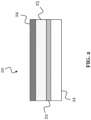
- FIG. 2 shows schematically a memory cell 20 according to an embodiment of this disclosure.
- the memory cell 20 may be a memory cell of a memory device according to another embodiment.
- This memory device may include a plurality of such memory cells 20.
- the memory device may, in particular, be a NAND type memory device, i.e., multiple of the memory cells 20 may be connected to each other in at least one NAND string.
- the memory device maybe a 3D memory device, wherein one or more NAND strings may be formed in a gate all around structure.
- the memory device may, for example, be a DRAM device, a SCM device, or a Flash memory device, i.e., the memory cell 20 is suitable for any such memory device.
- the memory cell 20 includes a semiconductor layer 21, which for instance, comprises a silicon layer, or a silicon-based layer, or a semiconductor-oxide layer. Further, the memory cell 20 includes a tunnel layer 22, which is arranged directly on the semiconductor layer 21. The tunnel layer 22 may comprise an oxide layer, like a silicon oxide layer. Further, the memory cell 20 includes a ferroelectric trapping layer 23, which is arranged directly on the tunnel layer 22. Finally, it includes a conductive gate layer 24 that is arranged directly on the ferroelectric trapping layer 23.
- the ferroelectric trapping layer 23 may comprise at least one of a hafnium oxide layer and a hafnium zirconium oxide layer.
- the gate layer 24 may comprise a metal layer, like a titanium nitride layer, and may be formed as a metal gate structure.
- the layers 21, 22, 23, 24 of the memory cell 20 form a layer stack of the memory cell 20.
- the conductive gate layer 24 may be formed first, and the semiconductor layer 21 may be formed last, as described below.
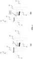
- FIG. 3 shows schematically a band-diagram of the memory cell 20 shown in FIG. 2 . Same layers of the memory cell 20 are labelled with the same reference signs in FIG. 2 and in FIG. 3 . In particular - similar as shown for the memory cell 10 in FIG. 1 - FIG. 3(a) shows a start of programming the memory cell 20, and FIG. 3(b) shows an end of programming the memory cell 20.
- the band diagram is similar to the band diagram of the memory cell 10 of the conventional Flash memory shown in FIG. 1 (of course, in FIG. 3 there is no blocking layer between the ferroelectric charge trapping layer 23 and the conductive gate layer 24).
- the ferroelectric trapping layer 23 switches polarity upon applying the programming pulse (e.g., applying a positive voltage above a determined threshold voltage to the conductive gate layer 24)
- the electric field in the trapping layer 23 may reverse.
- the ferroelectric trapping layer 23 may be arranged such that its positively polarized side is in contact with the tunnel layer 22, and its negatively polarized side is in contact with the conductive gate layer 24, if the programming voltage is applied to the conductive gate layer 24.
- the electron injection is lower, and the trapped electrons cause a band bending, however, only at the interface of the charge trapping layer 23 and the tunnel layer 22. This keeps the force on the electrons directed towards this interface (rather than being directed towards the conductive gate layer 24).
- no blocking layer is needed between the trapping layer 23 and the gate layer 24 (i.e., it is not necessarily required for achieving sufficient retention time).
- a blocking layer like an oxide layer, could still be added to the memory cell 20 between the ferroelectric charge trapping layer 23 and the conductive gate layer 24, in order to increase the retention of the memory cell 20 further, if so desired.
- the complexity of the memory cell 20 is lower, which is preferable.
- the ferroelectric trapping layer 23 can be used for the purpose of electron trapping, since the ferroelectric material contains defects that are suitable for electron trapping (e.g., doped hafnium oxide and hafnium zirconium oxide are particularly suitable ferroelectric materials for this purpose). Further, the ferroelectric trapping layer 23 has a permanent dipole, which changes the internal field inside the trapping layer 23. This field can be oriented against the applied voltage, i.e., against the programming voltage applied to the memory cell during programming, because of the substantial size of the dipole of the ferroelectric trapping layer 23. Since moreover the ferroelectric trapping layer 23 is in contact with the tunnel layer 22, the voltage drop over the tunnel layer 22 may change drastically when the ferroelectric trapping layer 23 switches its polarity upon applying the programming voltage.
- ferroelectric field of the ferroelectric trapping layer 23 being oriented against the tunnel layer field during the programming of the memory cell 20 is, that the electrons in the charge trapping layer 23 will be pushed back into an area near the tunnel layer-ferroelectric interface (see FIG. 3 ). This ensures a large window, since the trapped electrons are preferentially close to the semiconductor layer 21, and since they are not uniformly distributed inside the ferroelectric trapping layer 23. Further, this ensures a good retention of the memory cell 20, since no force drives the electrons out of the ferroelectric trapping layer 23 - in contrast to what is shown in FIG. 1 . The good retention allows skipping the blocking layer, which is typically needed in a conventional Flash memory (see the blocking layer 14 in FIG. 1 ).
- the equivalent oxide thickness (EOT) of the layer stack of the memory cell 20 is drastically smaller (also considering the intrinsically high dielectric constant of ferroelectrics), which may further help to scale even further a memory device that includes one or more such memory cell(s) 20 (e.g., in a 3D NAND where the stack thickness is in the pitch twice), and may also increase the read current, which helps for faster access times.
- the memory cell 20 shown in FIG. 2 and 3 allow for a memory device which is faster (in read as well as in write) without sacrificing density (on the contrary). Therefore, the memory device may replace a Flash memory and/or may also serve as a SCM between a conventional Flash memory and a DRAM. Also, the write pulse (i.e., the programming voltage pulse) may be much smaller in amplitude, which enables to provide more bandwidth but also at lower cost, since the high voltage circuitry may be designed substantially smaller. Notably, the memory cell 20 proposed by this disclosure is backwards compatible with the currently used 3D NAND flows.
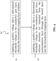
- FIG. 4 shows a method 40 according to an embodiment of this disclosure.
- the method 40 is for operating a memory cell of a memory device.
- the memory cell 20 may be implemented as shown in FIG. 2 and FIG.3 , i.e., based on the same layer stack including layers 21, 22, 23, 24.
- the method 40 comprises - for programming the memory cell - a step 41 of applying 41 a positive voltage above a determined threshold voltage to the conductive gate layer 24, wherein the ferroelectric trapping layer 23 switches its polarity such that its positively polarized side is formed in contact with the tunnel layer. Further, the method 40 comprises a step 42 of (still) applying a positive voltage above a determined threshold voltage to the conductive gate layer 24, wherein electrons are tunneled from the semiconductor layer 21 through the tunnel layer 22 into the ferroelectric trapping layer 23. These steps resemble the scenario shown in FIG. 3 .
- the method 40 may comprise - for erasing the memory cell - a step of applying a voltage below the determined threshold voltage to the conductive gate layer 24.
- the ferroelectric layer 23 switches again its polarity, such that its negatively polarized side is formed in contact with the tunnel layer 22. This leads to the trapped electrons 33 in the ferroelectric trapping layer 23 tunneling from the ferroelectric trapping layer 23 through the tunnel layer 22 into the semiconductor layer 21.
- FIG. 5 shows a method 50 according to an embodiment of this disclosure.
- the method 50 is for fabricating a memory cell 20 of a memory device.
- the memory cell 20 may be the one shown in FIG. 2 and FIG.3 , i.e., may be based on the layer stack.
- the method 50 comprises a step 51 of forming the conductive gate layer 24. Then, the method 50 comprises a step 52 of forming the ferroelectric trapping layer 23 directly on the conductive gate layer 24, a step 53 of forming the tunnel layer 22 directly on the ferroelectric trapping layer 23, and finally a step 54 of forming the semiconductor layer 21 directly on the tunnel layer 22.
- the memory cell 20 may accordingly be fabricated in a channel-last approach (semiconductor layer 21 acting as channel), in particular, if the memory cell 20 has a gate all around structure. For example, after the conductive gate layer 24 is formed, a hole or trench maybe formed in the conductive gate layer 24. Then, after the hole or trench is made in the conductive gate layer 24, the remaining layers 23, 22, 12 are formed in the hole or trench from the conductive gate layer 24 towards the semiconductor layer 21. Thus, the memory cell 20 maybe built up sideways in the hole or trench.
- the method 50 may alternatively comprise first a step of forming the semiconductor layer 21.
- the method 50 may further comprise a step of forming the tunnel layer 22 directly on the semiconductor layer 21, a step 53 of forming the ferroelectric trapping layer 23 directly on the tunnel layer 22, and finally a step of forming 54 the conductive gate layer 24 directly on the ferroelectric trapping layer 23.
- the individual layers 21, 22, 23, 24 may in each alternative of the method 50 be formed by chemical vapor deposition and/or by atomic layer deposition. However, also an epitaxial growth or another deposition techniques maybe used to form the individual layers 21, 22, 23, 24 of the memory cell 20.
- this disclosure exploits the trapping capability of a metal-ferroelectric-interface-semiconductor stack, to propose a much more efficient stack with lower operating voltages and better electrical characteristics (read/write speed).
Landscapes
- Engineering & Computer Science (AREA)
- Computer Hardware Design (AREA)
- Non-Volatile Memory (AREA)
Abstract
Description
- The present disclosure relates to memory devices, in particular, to Flash memory devices, storage class memory (SCM) devices, and dynamic random access memory (DRAM) devices. The disclosure provides a memory device with at least one memory cell that includes a ferroelectric charge trapping layer. Further, the memory cell does not include a blocking layer between the ferroelectric charge trapping layer and a gate layer.
- Conventional Flash memories, in particular of the charge trapping type, rely on the tunneling of electrons for programming and erasing a memory cell, respectively (e.g., in a NAND type memory device).
-
FIG. 1 shows a band-diagram of anexemplary memory cell 10 of such a conventional Flash memory. Thememory cell 10 includes a semiconductor layer 11 (typically silicon), a tunnel layer 12 (typically silicon oxide), a charge trapping layer 13 (typically silicon nitride), a blocking layer 14 (typically silicon oxide), and ametal gate 15. - FIG. i(a) shows that at a beginning of a voltage pulse for programming the
memory cell 10, a high number of electrons are injected from thesemiconductor layer 11 into thecharge trapping layer 13 by tunneling through thetunnel layer 12. Thecharge trapping layer 13 comprises traps, which are suitable for capturing electrons. The electric field in the charge trappinglayer 13 during programming pushes electrons away from the interface between thecharge trapping layer 13 and thetunnel layer 12. - FIG. i(b) shows further that at the end of the programming pulse, the electron injection is lower, and electrons are now trapped in the
charge trapping layer 13. The trapped electrons cause a band bending in the charge trappinglayer 13, which increases the force on the electrons away from the trapping sites towards thegate 15. Therefore, theblocking layer 14 is required for a sufficient retention time of thememory cell 10. However, also thetunnel layer 12 is needed to prevent electrons from escaping towards thesemiconductor layer 11, and to thus guarantee the retention time. - Such a conventional Flash memory suffers from a very high programming/erasing voltage requirement. The reason is that the
tunnel layer 12 has to be relatively thick for achieving a good retention time (typically, the retention time is desired to be in the order of years). Moreover, the blockinglayer 14 adds to the complexity of thememory cell 10, and particularly to increased costs of manufacturing the conventional Flash memory. - As a consequence of the
tunnel layer 12, even with programming voltages as high as 20 V, for example, the programming time of thememory cell 10 is still in the order of 100 µs, which is extremely slow compared to the speed of current electronics (e.g. of a current central processing unit (CPU)). Therefore, the conventional Flash memory cannot directly communicate with such a CPU, or with a microprocessor or microcontroller, and therefore intermediate memory levels are required. For instance, a memory hierarchy may be used for bridging this speed gap, wherein a DRAM connects to the CPU, and a SCM connects the DRAM and the Flash memory. - If a Flash memory device with higher speeds could be obtained, preferably also at lower programming voltages, then the Flash memory could communicate directly with the DRAM, without the need for an intermediate SCM. Alternatively, such a high-speed memory device could be used as SCM in the above-mentioned memory hierarchy. Both approaches would significantly reduce the cost of the whole memory system.
- The present disclosure and its embodiments are based further on the following considerations of the inventors. Generally, the inventors considered that including a ferroelectric layer in a Flash memory cell may be beneficial for reducing the required programming voltage.
- Moreover, because of the difficult voltage-retention trade-off, some 3D NAND type memories use a gate all around structure, which enhances the field in the tunnel layer by using the curvature of the memory hole. The density could even be doubled, if it would be possible to apply a trench architecture, as explained in
US patent 10,522,624 B2 - Exemplary approaches of including a ferroelectric layer into a Flash memory cell comprise: (a) using a ferroelectric blocking layer arranged on a conventional charge trapping layer; or (b) using an additional ferroelectric blocking layer arranged on a conventional blocking layer; or (c) using a ferroelectric trapping layer with a conventional blocking layer formed on top of it.
- However, these exemplary approaches either do not overcome the above-mentioned problems related to the programming voltage of the Flash memory device, or require a large number of layers that adds to the complexity and cost of (manufacturing) the memory device.
- In view of the above, this disclosure has the objective to provide an improved memory cell for a memory device - for instance, for a Flash memory device, a SCM device, or a DRAM device - wherein the memory cell can be programmed faster and with a lower programming voltage. Thereby, another objective of this disclosure is to introduce a ferroelectric layer into the memory cell in such a way, that it does not add to the complexity and manufacturing cost of the memory cell. These and other objectives are achieved by the embodiments of this disclosure provided in the enclosed independent claims. Advantageous implementations of the embodiments are defined in the dependent claims.
- In particular, the embodiments of this disclosure are based on a memory cell that includes a ferroelectric layer as a charge trapping layer (i.e., a ferroelectric trapping layer), and that does not include any blocking layer between the charge trapping layer and the gate (layer).
- A first aspect of this disclosure provides a memory cell for a memory device, wherein the memory cell comprises a layer stack including: a semiconductor layer; a tunnel layer provided directly on the semiconductor layer; a ferroelectric trapping layer provided directly on the tunnel layer; and a conductive gate layer provided directly on the ferroelectric trapping layer.
- The memory cell of the first aspect thus comprises a ferroelectric layer as a charge trapping layer. This reduces the programming voltage that is needed to program the memory cell, i.e., to effect tunneling of electrons from the semiconductor layer into the ferroelectric trapping layer, in which the electrons may be trapped. Further, the ferroelectric trapping layer allows omitting a blocking layer between the charge trapping layer and the gate layer, i.e., the gate layer is provided directly on the ferroelectric trapping layer, without any in between layer.
- In particular, due to the ferroelectric trapping layer, a potential well can form at the interface between the ferroelectric trapping layer and the tunnel layer during the programming of the memory cell. Further, a force on trapped electrons in the ferroelectric trapping layer is directed towards the tunnel layer during the programming, and not towards the gate layer. Accordingly, the memory cell can have a sufficient retention time even without the use of a blocking layer between the ferroelectric trapping layer and the gate layer.
- In an implementation of the memory cell, the ferroelectric trapping layer is configured and arranged such that its positively polarized side is in contact with the tunnel layer and its negatively polarized side is in contact with the conductive gate layer, if a positive voltage above a determined threshold voltage is applied to the conductive gate layer.
- This favors the formation of the above-described potential well in the ferroelectric trapping layer at the tunnel layer interface.
- In an implementation of the memory cell, the ferroelectric trapping layer comprises at least one of a hafnium oxide layer and a hafnium zirconium oxide layer.
- In an implementation of the memory cell, the tunnel layer comprises at least one of a dielectric layer and an oxide layer.
- In an implementation of the memory cell, the semiconductor layer comprises at least one of a silicon layer, a silicon-based layer, an oxide semiconductor, and an indium gallium zinc oxide.
- In an implementation of the memory cell, the conductive gate layer comprises a metal layer or a titanium nitride layer.
- In an implementation of the memory cell, the semiconductor layer is a semiconductor channel; the tunnel layer surrounds the semiconductor channel; the ferroelectric trapping layer surrounds the tunnel layer and the semiconductor channel; and the conductive gate layer surrounds the ferroelectric trapping layer, the tunnel layer, and the semiconductor channel.
- Accordingly, a memory cell (or a string of multiple memory cells) having a gate all around structure may be realized.
- A second aspect provides a memory device comprising a plurality of memory cells, wherein each of the plurality of memory cells is implemented according to the first aspect or any of its implementations described above.
- Thus, a memory device maybe realized, which has a sufficient retention time, while it also requires a lower programming voltage for its memory cell(s) - and thus enables higher programming speeds than a conventional Flash memory.
- In an implementation of the memory device, the plurality of memory cells are connected to each other and form a NAND string.
- That is, a NAND type memory device maybe realized, which may have one or more such NAND strings.
- In an implementation, the memory device is a 3D memory device and, for each memory cell of the plurality of memory cells, the semiconductor layer is a semiconductor channel, the tunnel layer surrounds the semiconductor channel, the ferroelectric trapping layer surrounds the tunnel layer and the semiconductor channel, and the conductive gate layer surrounds the ferroelectric trapping layer, the tunnel layer, and the semiconductor channel.
- Accordingly, a 3D memory device, for example, a 3D NAND type memory device may be realized. Each of one or more NAND strings of such a 3D memory device maybe implemented in a gate all around structure.
- In an implementation, the memory device is a DRAM device or a SCM device or a Flash memory device.
- The memory device of the second aspect may replace a conventional Flash memory device, or may act as a SCM device arranged between a conventional DRAM device and a conventional Flash memory device (e.g., in a memory hierarchy as described above). The memory device of the second aspect may even replace a conventional DRAM device.
- A third aspect of this disclosure provides a method for operating a memory cell of a memory device, where the memory cell is implemented according to the first aspect or any implementation thereof, wherein the method comprises: applying a positive voltage above a determined threshold voltage to the conductive gate layer, wherein the ferroelectric trapping layer switches its polarity such that its positively polarized side is formed in contact with the tunnel layer; and electrons are tunneled from the semiconductor layer through the tunnel layer into the ferroelectric trapping layer.
- In this way the memory cell may be programmed, wherein a programming voltage can be much lower than in a conventional (Flash) memory device, due to the ferroelectric trapping layer.
- In an implementation of the third aspect, at least a part of the electrons, which are tunneled from the semiconductor layer through the tunnel layer into the ferroelectric trapping layer, are trapped in defects of the ferroelectric trapping layer and/or are captured in a potential well formed at an interface of the tunnel layer and the ferroelectric trapping layer.
- Thus, the retention time of the memory cell is sufficiently high, even though the memory cell does not have the blocking layer of the conventional memory cell shown in
FIG. 1 . - In an implementation of the third aspect, the method further comprises applying a voltage below the determined threshold voltage to the conductive gate layer, wherein the ferroelectric layer switches its polarity such that its negatively polarized side is formed in contact with the tunnel layer; and the trapped electrons in the ferroelectric trapping layer are tunneled from the ferroelectric trapping layer through the tunnel layer into the semiconductor layer.
- In particular, applying the voltage below the determined threshold voltage may comprise applying the voltage below another determined negative threshold voltage. In this way the memory cell can be erased. Thereby, the erasing voltage may be lower in absolute value than in a conventional (Flash) memory device.
- A fourth aspect of this disclosure provides a method for fabricating a memory cell for a memory device, wherein the method comprises: forming a semiconductor layer; forming tunnel layer directly on the semiconductor layer; forming a ferroelectric trapping layer directly on the tunnel layer; and forming a conductive gate layer directly on the ferroelectric trapping layer.
- The method of the fourth aspect may produce the memory cell of the first aspect and any implementation thereof, and further the memory device of the second aspect. The method of the fourth aspect achieves the same advantages as the memory cell and memory device of the first and second aspect, respectively, and may be extended by respective implementations as described above for the memory device of the first aspect.
- The above described aspects and implementations are explained in the following description of embodiments with respect to the enclosed drawings:
- FIG. 1
- shows a band-diagram of a memory cell of a conventional Flash memory during the programming of the memory cell.
- FIG. 2
- shows a memory cell according to an embodiment of this disclosure including multiple layers.
- FIG. 3
- shows a band-diagram of a memory cell according to an embodiment of this disclosure, during the programming of the memory cell.
- FIG. 4
- shows a flow diagram of a method for operating a memory cell according to an embodiment of this disclosure.
- FIG. 5
- shows a flow diagram of a method for fabricating a memory cell according to an embodiment of this disclosure.
-
FIG. 2 shows schematically amemory cell 20 according to an embodiment of this disclosure. Thememory cell 20 may be a memory cell of a memory device according to another embodiment. This memory device may include a plurality ofsuch memory cells 20. The memory device may, in particular, be a NAND type memory device, i.e., multiple of thememory cells 20 may be connected to each other in at least one NAND string. The memory device maybe a 3D memory device, wherein one or more NAND strings may be formed in a gate all around structure. The memory device may, for example, be a DRAM device, a SCM device, or a Flash memory device, i.e., thememory cell 20 is suitable for any such memory device. - As shown in
FIG. 2 , thememory cell 20 includes asemiconductor layer 21, which for instance, comprises a silicon layer, or a silicon-based layer, or a semiconductor-oxide layer. Further, thememory cell 20 includes atunnel layer 22, which is arranged directly on thesemiconductor layer 21. Thetunnel layer 22 may comprise an oxide layer, like a silicon oxide layer. Further, thememory cell 20 includes aferroelectric trapping layer 23, which is arranged directly on thetunnel layer 22. Finally, it includes aconductive gate layer 24 that is arranged directly on theferroelectric trapping layer 23. Theferroelectric trapping layer 23 may comprise at least one of a hafnium oxide layer and a hafnium zirconium oxide layer. Thegate layer 24 may comprise a metal layer, like a titanium nitride layer, and may be formed as a metal gate structure. Thelayers memory cell 20 form a layer stack of thememory cell 20. Notably, of thelayers conductive gate layer 24 may be formed first, and thesemiconductor layer 21 may be formed last, as described below. -
FIG. 3 shows schematically a band-diagram of thememory cell 20 shown inFIG. 2 . Same layers of thememory cell 20 are labelled with the same reference signs inFIG. 2 and inFIG. 3 . In particular - similar as shown for thememory cell 10 inFIG. 1 - FIG. 3(a) shows a start of programming thememory cell 20, andFIG. 3(b) shows an end of programming thememory cell 20. - At the start of the programming of the
memory cell 20, the band diagram is similar to the band diagram of thememory cell 10 of the conventional Flash memory shown inFIG. 1 (of course, inFIG. 3 there is no blocking layer between the ferroelectriccharge trapping layer 23 and the conductive gate layer 24). When theferroelectric trapping layer 23 switches polarity upon applying the programming pulse (e.g., applying a positive voltage above a determined threshold voltage to the conductive gate layer 24), the electric field in thetrapping layer 23 may reverse. In particular, theferroelectric trapping layer 23 may be arranged such that its positively polarized side is in contact with thetunnel layer 22, and its negatively polarized side is in contact with theconductive gate layer 24, if the programming voltage is applied to theconductive gate layer 24. As a consequence, a large field drops over thetunnel layer 22, and further a much lower programming voltage is required compared to the conventional Flash memory shown inFIG. 1 . Because of the electric field reversal, the electrons that tunnel through thetunnel layer 22 into theferroelectric trapping layer 23 may moreover be trapped predominantly at the interface of saidlayer 23 to the tunnel layer 22 (which may lead to larger Vth shift for the same charge). - At the end of programming the
memory cell 20, the electron injection is lower, and the trapped electrons cause a band bending, however, only at the interface of thecharge trapping layer 23 and thetunnel layer 22. This keeps the force on the electrons directed towards this interface (rather than being directed towards the conductive gate layer 24). As a consequence, no blocking layer is needed between the trappinglayer 23 and the gate layer 24 (i.e., it is not necessarily required for achieving sufficient retention time). Of course, a blocking layer, like an oxide layer, could still be added to thememory cell 20 between the ferroelectriccharge trapping layer 23 and theconductive gate layer 24, in order to increase the retention of thememory cell 20 further, if so desired. However, without the blocking layer, the complexity of thememory cell 20 is lower, which is preferable. - In the following, some more details and explanations are given regarding the
memory cell 20 shown inFIG. 2 andFIG. 3 , respectively. Theferroelectric trapping layer 23 can be used for the purpose of electron trapping, since the ferroelectric material contains defects that are suitable for electron trapping (e.g., doped hafnium oxide and hafnium zirconium oxide are particularly suitable ferroelectric materials for this purpose). Further, theferroelectric trapping layer 23 has a permanent dipole, which changes the internal field inside thetrapping layer 23. This field can be oriented against the applied voltage, i.e., against the programming voltage applied to the memory cell during programming, because of the substantial size of the dipole of theferroelectric trapping layer 23. Since moreover theferroelectric trapping layer 23 is in contact with thetunnel layer 22, the voltage drop over thetunnel layer 22 may change drastically when theferroelectric trapping layer 23 switches its polarity upon applying the programming voltage. - Another advantage of the ferroelectric field of the
ferroelectric trapping layer 23 being oriented against the tunnel layer field during the programming of thememory cell 20 is, that the electrons in thecharge trapping layer 23 will be pushed back into an area near the tunnel layer-ferroelectric interface (seeFIG. 3 ). This ensures a large window, since the trapped electrons are preferentially close to thesemiconductor layer 21, and since they are not uniformly distributed inside theferroelectric trapping layer 23. Further, this ensures a good retention of thememory cell 20, since no force drives the electrons out of the ferroelectric trapping layer 23 - in contrast to what is shown inFIG. 1 . The good retention allows skipping the blocking layer, which is typically needed in a conventional Flash memory (see theblocking layer 14 inFIG. 1 ). - As a result, the equivalent oxide thickness (EOT) of the layer stack of the
memory cell 20 is drastically smaller (also considering the intrinsically high dielectric constant of ferroelectrics), which may further help to scale even further a memory device that includes one or more such memory cell(s) 20 (e.g., in a 3D NAND where the stack thickness is in the pitch twice), and may also increase the read current, which helps for faster access times. - All these benefits of the
memory cell 20 shown inFIG. 2 and3 , respectively, allow for a memory device which is faster (in read as well as in write) without sacrificing density (on the contrary). Therefore, the memory device may replace a Flash memory and/or may also serve as a SCM between a conventional Flash memory and a DRAM. Also, the write pulse (i.e., the programming voltage pulse) may be much smaller in amplitude, which enables to provide more bandwidth but also at lower cost, since the high voltage circuitry may be designed substantially smaller. Notably, thememory cell 20 proposed by this disclosure is backwards compatible with the currently used 3D NAND flows. -
FIG. 4 shows amethod 40 according to an embodiment of this disclosure. Themethod 40 is for operating a memory cell of a memory device. Thememory cell 20 may be implemented as shown inFIG. 2 andFIG.3 , i.e., based on the same layerstack including layers - The
method 40 comprises - for programming the memory cell - astep 41 of applying 41 a positive voltage above a determined threshold voltage to theconductive gate layer 24, wherein theferroelectric trapping layer 23 switches its polarity such that its positively polarized side is formed in contact with the tunnel layer. Further, themethod 40 comprises astep 42 of (still) applying a positive voltage above a determined threshold voltage to theconductive gate layer 24, wherein electrons are tunneled from thesemiconductor layer 21 through thetunnel layer 22 into theferroelectric trapping layer 23. These steps resemble the scenario shown inFIG. 3 . - Further, the
method 40 may comprise - for erasing the memory cell - a step of applying a voltage below the determined threshold voltage to theconductive gate layer 24. In this case, theferroelectric layer 23 switches again its polarity, such that its negatively polarized side is formed in contact with thetunnel layer 22. This leads to the trappedelectrons 33 in theferroelectric trapping layer 23 tunneling from theferroelectric trapping layer 23 through thetunnel layer 22 into thesemiconductor layer 21. - That is, for the erasing, a similar effect can be used to remove the electrons and eventually trap holes in the ferroelectric trapping layer 23 (the ferroelectric dipole flips back to enhance the tunnel oxide field in the other direction).
-
FIG. 5 shows amethod 50 according to an embodiment of this disclosure. Themethod 50 is for fabricating amemory cell 20 of a memory device. Thememory cell 20 may be the one shown inFIG. 2 andFIG.3 , i.e., may be based on the layer stack. - The
method 50 comprises astep 51 of forming theconductive gate layer 24. Then, themethod 50 comprises astep 52 of forming theferroelectric trapping layer 23 directly on theconductive gate layer 24, astep 53 of forming thetunnel layer 22 directly on theferroelectric trapping layer 23, and finally astep 54 of forming thesemiconductor layer 21 directly on thetunnel layer 22. Thememory cell 20 may accordingly be fabricated in a channel-last approach (semiconductor layer 21 acting as channel), in particular, if thememory cell 20 has a gate all around structure. For example, after theconductive gate layer 24 is formed, a hole or trench maybe formed in theconductive gate layer 24. Then, after the hole or trench is made in theconductive gate layer 24, the remaininglayers conductive gate layer 24 towards thesemiconductor layer 21. Thus, thememory cell 20 maybe built up sideways in the hole or trench. - The
method 50 may alternatively comprise first a step of forming thesemiconductor layer 21. In this case, themethod 50 may further comprise a step of forming thetunnel layer 22 directly on thesemiconductor layer 21, astep 53 of forming theferroelectric trapping layer 23 directly on thetunnel layer 22, and finally a step of forming 54 theconductive gate layer 24 directly on theferroelectric trapping layer 23. - The
individual layers method 50 be formed by chemical vapor deposition and/or by atomic layer deposition. However, also an epitaxial growth or another deposition techniques maybe used to form theindividual layers memory cell 20. - In summary, this disclosure exploits the trapping capability of a metal-ferroelectric-interface-semiconductor stack, to propose a much more efficient stack with lower operating voltages and better electrical characteristics (read/write speed).
Claims (15)
- A memory cell (20) for a memory device, wherein the memory cell (20) comprises a layer stack including:a semiconductor layer (21);a tunnel layer (22) provided directly on the semiconductor layer (21);a ferroelectric trapping layer (23) provided directly on the tunnel layer (22); anda conductive gate layer (24) provided directly on the ferroelectric trapping layer (23).
- The memory cell (20) according to claim 1, wherein the ferroelectric trapping layer (23) is configured and arranged such that its positively polarized side is in contact with the tunnel layer (22) and its negatively polarized side is in contact with the conductive gate layer (24), if a positive voltage above a determined threshold voltage is applied to the conductive gate layer (24).
- The memory cell (20) according to claim 1 or 2, wherein the ferroelectric trapping layer (23) comprises at least one of a hafnium oxide layer and a hafnium zirconium oxide layer.
- The memory cell (20) according to one of the claims 1 to 3, wherein the tunnel layer (22) comprises at least one of a dielectric layer and an oxide layer.
- The memory cell (20) according to one of the claims 1 to 4, wherein the semiconductor layer (21) comprises at least one of a silicon layer, a silicon-based layer, an oxide semiconductor, and an indium gallium zinc oxide.
- The memory cell (20) according to one of the claims 1 to 5, wherein the conductive gate layer (24) comprises a metal layer or a titanium nitride layer.
- The memory cell (20) according to one of the claims 1 to 6, wherein:the semiconductor layer (21) is a semiconductor channel;the tunnel layer (22) surrounds the semiconductor channel (21);the ferroelectric trapping layer (23) surrounds the tunnel layer (22) and the semiconductor channel (21); andthe conductive gate layer (24) surrounds the ferroelectric trapping layer (23), the tunnel layer (22), and the semiconductor channel (21).
- A memory device comprising a plurality of memory cells (20), wherein each of the plurality of memory cells (20) is implemented according to one of the claims 1 to 7.
- The memory device according to claim 8, wherein the plurality of memory cells (20) are connected to each other and form a NAND string.
- The memory device according to claim 8 or 9, wherein the memory device is a 3D memory device and each memory cell (20) of the plurality of memory cells (20) is implemented according to claim 7.
- The memory device according to one of the claims 8 to 10, wherein the memory device is a Dynamic Random Access Memory, DRAM, device, or a Storage Class Memory, SCM, device.
- A method (40) for operating a memory cell (20) of a memory device, wherein the memory cell (20) is implemented according to one of the claims 1 to 7, and wherein the method (40) comprises:
applying (41, 42) a positive voltage above a determined threshold voltage to the conductive gate layer (24), wherein- the ferroelectric trapping layer (23) switches (41) its polarity such that its positively polarized side is formed in contact with the tunnel layer (22); and- electrons are tunneled (42) from the semiconductor layer (21) through the tunnel layer (22) into the ferroelectric trapping layer (23). - The method (40) for according to claim 12, wherein at least a part of the electrons, which are tunneled (42) from the semiconductor layer (21) through the tunnel layer (22) into the ferroelectric trapping layer (23), are trapped in defects (32) of the ferroelectric trapping layer (23) and/or are captured in a potential well (31) formed at an interface of the tunnel layer (22) and the ferroelectric trapping layer (23).
- The method (40) according to claim 13, further comprising:
applying a voltage below the determined threshold voltage to the conductive gate layer (24), wherein- the ferroelectric layer (23) switches its polarity such that its negatively polarized side is formed in contact with the tunnel layer (22); and- the trapped electrons (33) in the ferroelectric trapping layer (23) are tunneled from the ferroelectric trapping layer (23) through the tunnel layer (22) into the semiconductor layer (21). - A method (50) for fabricating a memory cell (20) for a memory device, wherein the method comprises:forming (51) a conductive gate layer (24);forming (52) a ferroelectric trapping layer (23) directly on the conductive gate layer (24);forming (53) a tunnel layer (22) directly on the ferroelectric trapping layer (23); andforming (54) a semiconductor layer (21) directly on the tunnel layer (22).
Priority Applications (2)
| Application Number | Priority Date | Filing Date | Title |
|---|---|---|---|
| EP21190723.3A EP4135009A1 (en) | 2021-08-11 | 2021-08-11 | A memory device with a ferroelectric charge trapping layer |
| US17/817,550 US12041782B2 (en) | 2021-08-11 | 2022-08-04 | Memory device with ferroelectric charge trapping layer |
Applications Claiming Priority (1)
| Application Number | Priority Date | Filing Date | Title |
|---|---|---|---|
| EP21190723.3A EP4135009A1 (en) | 2021-08-11 | 2021-08-11 | A memory device with a ferroelectric charge trapping layer |
Publications (1)
| Publication Number | Publication Date |
|---|---|
| EP4135009A1 true EP4135009A1 (en) | 2023-02-15 |
Family
ID=77411552
Family Applications (1)
| Application Number | Title | Priority Date | Filing Date |
|---|---|---|---|
| EP21190723.3A Pending EP4135009A1 (en) | 2021-08-11 | 2021-08-11 | A memory device with a ferroelectric charge trapping layer |
Country Status (2)
| Country | Link |
|---|---|
| US (1) | US12041782B2 (en) |
| EP (1) | EP4135009A1 (en) |
Citations (4)
| Publication number | Priority date | Publication date | Assignee | Title |
|---|---|---|---|---|
| US20040041186A1 (en) * | 2002-08-28 | 2004-03-04 | Klaus Dimmler | Ferroelectric transistor with enhanced data retention |
| US20180308537A1 (en) * | 2014-04-24 | 2018-10-25 | Micron Technology, Inc. | Field Effect Transistor Constructions With Gate Insulator Having Local Regions Radially There-Through That Have Different Capacitance At Different Circumferential Locations Relative To A Channel Core Periphery |
| US20190057860A1 (en) * | 2017-08-18 | 2019-02-21 | Lam Research Corporation | Methods for improving performance in hafnium oxide-based ferroelectric material using plasma and/or thermal treatment |
| US20210028180A1 (en) * | 2019-07-25 | 2021-01-28 | Renesas Electronics Corporation | Semiconductor device and method of manufacturing the same |
Family Cites Families (10)
| Publication number | Priority date | Publication date | Assignee | Title |
|---|---|---|---|---|
| KR20000018524A (en) * | 1998-09-02 | 2000-04-06 | 김영환 | Non volatile memory device and a manufacturing method thereof |
| US7378286B2 (en) * | 2004-08-20 | 2008-05-27 | Sharp Laboratories Of America, Inc. | Semiconductive metal oxide thin film ferroelectric memory transistor |
| US20070190721A1 (en) * | 2006-02-16 | 2007-08-16 | Samsung Electronics Co., Ltd. | Semiconductor memory device having an alloy metal gate electrode and method of manufacturing the same |
| US20100117141A1 (en) * | 2008-11-13 | 2010-05-13 | Samsung Electronics Co., Ltd. | Memory cell transistors having limited charge spreading, non-volatile memory devices including such transistors, and methods of formation thereof |
| US9508439B2 (en) * | 2014-07-11 | 2016-11-29 | Qualcomm Incorporated | Non-volatile multiple time programmable memory device |
| TW201637172A (en) * | 2015-04-14 | 2016-10-16 | 國立交通大學 | Memory structure |
| US10522624B2 (en) | 2016-12-27 | 2019-12-31 | Imec Vzw | V-grooved vertical channel-type 3D semiconductor memory device and method for manufacturing the same |
| US11515330B2 (en) * | 2019-05-10 | 2022-11-29 | Yung-Tin Chen | Three-dimensional ferroelectric random-access memory (FeRAM) |
| WO2022164659A1 (en) * | 2021-01-27 | 2022-08-04 | Sunrise Memory Corporation | Quasi-volatile memory with reference bit line structure |
| JP2023001408A (en) * | 2021-06-17 | 2023-01-06 | キオクシア株式会社 | Semiconductor memory device |
-
2021
- 2021-08-11 EP EP21190723.3A patent/EP4135009A1/en active Pending
-
2022
- 2022-08-04 US US17/817,550 patent/US12041782B2/en active Active
Patent Citations (4)
| Publication number | Priority date | Publication date | Assignee | Title |
|---|---|---|---|---|
| US20040041186A1 (en) * | 2002-08-28 | 2004-03-04 | Klaus Dimmler | Ferroelectric transistor with enhanced data retention |
| US20180308537A1 (en) * | 2014-04-24 | 2018-10-25 | Micron Technology, Inc. | Field Effect Transistor Constructions With Gate Insulator Having Local Regions Radially There-Through That Have Different Capacitance At Different Circumferential Locations Relative To A Channel Core Periphery |
| US20190057860A1 (en) * | 2017-08-18 | 2019-02-21 | Lam Research Corporation | Methods for improving performance in hafnium oxide-based ferroelectric material using plasma and/or thermal treatment |
| US20210028180A1 (en) * | 2019-07-25 | 2021-01-28 | Renesas Electronics Corporation | Semiconductor device and method of manufacturing the same |
Non-Patent Citations (1)
| Title |
|---|
| MULAOSMANOVIC HALID ET AL: "Switching and Charge Trapping in HfO2-based Ferroelectric FETs: An Overview and Potential Applications", 2020 4TH IEEE ELECTRON DEVICES TECHNOLOGY & MANUFACTURING CONFERENCE (EDTM), IEEE, 6 April 2020 (2020-04-06), pages 1 - 4, XP033780735, [retrieved on 20200615], DOI: 10.1109/EDTM47692.2020.9118005 * |
Also Published As
| Publication number | Publication date |
|---|---|
| US12041782B2 (en) | 2024-07-16 |
| US20230262990A1 (en) | 2023-08-17 |
Similar Documents
| Publication | Publication Date | Title |
|---|---|---|
| US6847556B2 (en) | Method for operating NOR type flash memory device including SONOS cells | |
| US6255166B1 (en) | Nonvolatile memory cell, method of programming the same and nonvolatile memory array | |
| TWI388052B (en) | Memory element with separate gate and barrier layers | |
| JP3710082B2 (en) | How to make a memory transistor | |
| EP0495492B1 (en) | Non-volatile memory cell structure and process for forming same | |
| US20030042534A1 (en) | Scalable flash/NV structures and devices with extended endurance | |
| US6504755B1 (en) | Semiconductor memory device | |
| JPH10256400A (en) | Nonvolatile semiconductor memory device | |
| KR20060120078A (en) | Flash Memory Programming Using Gate-Induced Junction Leakage Current | |
| US7483309B2 (en) | Programming and erasing method for charge-trapping memory devices | |
| EP0062460A2 (en) | Electrically-erasable non-volatile semiconductor memory elements | |
| US20050167734A1 (en) | Flash memory devices using large electron affinity material for charge trapping | |
| CN101093839A (en) | memory element | |
| US8693255B2 (en) | Method for driving a nonvolatile semiconductor memory device | |
| US6724661B2 (en) | Erasing method in non-volatile memory device | |
| CN1841785A (en) | Split gate memory unit and method for manufacturing split gate memory unit array | |
| US20160111292A1 (en) | Charge trapping split gate embedded flash memory and associated methods | |
| TWI473253B (en) | Non-volatile memory array with continuous charge storage dielectric stack | |
| US7400538B2 (en) | NROM memory device with enhanced endurance | |
| US12041782B2 (en) | Memory device with ferroelectric charge trapping layer | |
| US20160218227A1 (en) | Gate Formation Memory by Planarization | |
| JP2000223598A (en) | Non-volatile memory device | |
| US11444208B2 (en) | Non-volatile memory device having low-k dielectric layer on sidewall of control gate electrode | |
| US7200040B2 (en) | Method of operating p-channel memory | |
| KR100868031B1 (en) | Nonvolatile memory device and method of manufacturing same |
Legal Events
| Date | Code | Title | Description |
|---|---|---|---|
| PUAI | Public reference made under article 153(3) epc to a published international application that has entered the european phase |
Free format text: ORIGINAL CODE: 0009012 |
|
| STAA | Information on the status of an ep patent application or granted ep patent |
Free format text: STATUS: THE APPLICATION HAS BEEN PUBLISHED |
|
| AK | Designated contracting states |
Kind code of ref document: A1 Designated state(s): AL AT BE BG CH CY CZ DE DK EE ES FI FR GB GR HR HU IE IS IT LI LT LU LV MC MK MT NL NO PL PT RO RS SE SI SK SM TR |
|
| STAA | Information on the status of an ep patent application or granted ep patent |
Free format text: STATUS: REQUEST FOR EXAMINATION WAS MADE |
|
| 17P | Request for examination filed |
Effective date: 20230802 |
|
| RBV | Designated contracting states (corrected) |
Designated state(s): AL AT BE BG CH CY CZ DE DK EE ES FI FR GB GR HR HU IE IS IT LI LT LU LV MC MK MT NL NO PL PT RO RS SE SI SK SM TR |
|
| STAA | Information on the status of an ep patent application or granted ep patent |
Free format text: STATUS: EXAMINATION IS IN PROGRESS |
|
| 17Q | First examination report despatched |
Effective date: 20260227 |