EP4134802A1 - Verfahren und vorrichtung für datenzugriff auf nand-flash-dateien und speichermedium - Google Patents
Verfahren und vorrichtung für datenzugriff auf nand-flash-dateien und speichermedium Download PDFInfo
- Publication number
- EP4134802A1 EP4134802A1 EP21785191.4A EP21785191A EP4134802A1 EP 4134802 A1 EP4134802 A1 EP 4134802A1 EP 21785191 A EP21785191 A EP 21785191A EP 4134802 A1 EP4134802 A1 EP 4134802A1
- Authority
- EP
- European Patent Office
- Prior art keywords
- storage space
- nand flash
- specified
- file
- data
- Prior art date
- Legal status (The legal status is an assumption and is not a legal conclusion. Google has not performed a legal analysis and makes no representation as to the accuracy of the status listed.)
- Granted
Links
Images


Classifications
-
- G—PHYSICS
- G06—COMPUTING OR CALCULATING; COUNTING
- G06F—ELECTRIC DIGITAL DATA PROCESSING
- G06F3/00—Input arrangements for transferring data to be processed into a form capable of being handled by the computer; Output arrangements for transferring data from processing unit to output unit, e.g. interface arrangements
- G06F3/06—Digital input from, or digital output to, record carriers, e.g. RAID, emulated record carriers or networked record carriers
- G06F3/0601—Interfaces specially adapted for storage systems
- G06F3/0628—Interfaces specially adapted for storage systems making use of a particular technique
- G06F3/0638—Organizing or formatting or addressing of data
- G06F3/0644—Management of space entities, e.g. partitions, extents, pools
-
- G—PHYSICS
- G06—COMPUTING OR CALCULATING; COUNTING
- G06F—ELECTRIC DIGITAL DATA PROCESSING
- G06F12/00—Accessing, addressing or allocating within memory systems or architectures
- G06F12/02—Addressing or allocation; Relocation
- G06F12/0223—User address space allocation, e.g. contiguous or non contiguous base addressing
- G06F12/023—Free address space management
- G06F12/0238—Memory management in non-volatile memory, e.g. resistive RAM or ferroelectric memory
- G06F12/0246—Memory management in non-volatile memory, e.g. resistive RAM or ferroelectric memory in block erasable memory, e.g. flash memory
-
- G—PHYSICS
- G06—COMPUTING OR CALCULATING; COUNTING
- G06F—ELECTRIC DIGITAL DATA PROCESSING
- G06F3/00—Input arrangements for transferring data to be processed into a form capable of being handled by the computer; Output arrangements for transferring data from processing unit to output unit, e.g. interface arrangements
- G06F3/06—Digital input from, or digital output to, record carriers, e.g. RAID, emulated record carriers or networked record carriers
- G06F3/0601—Interfaces specially adapted for storage systems
- G06F3/0602—Interfaces specially adapted for storage systems specifically adapted to achieve a particular effect
- G06F3/0604—Improving or facilitating administration, e.g. storage management
-
- G—PHYSICS
- G06—COMPUTING OR CALCULATING; COUNTING
- G06F—ELECTRIC DIGITAL DATA PROCESSING
- G06F3/00—Input arrangements for transferring data to be processed into a form capable of being handled by the computer; Output arrangements for transferring data from processing unit to output unit, e.g. interface arrangements
- G06F3/06—Digital input from, or digital output to, record carriers, e.g. RAID, emulated record carriers or networked record carriers
- G06F3/0601—Interfaces specially adapted for storage systems
- G06F3/0602—Interfaces specially adapted for storage systems specifically adapted to achieve a particular effect
- G06F3/061—Improving I/O performance
- G06F3/0611—Improving I/O performance in relation to response time
-
- G—PHYSICS
- G06—COMPUTING OR CALCULATING; COUNTING
- G06F—ELECTRIC DIGITAL DATA PROCESSING
- G06F3/00—Input arrangements for transferring data to be processed into a form capable of being handled by the computer; Output arrangements for transferring data from processing unit to output unit, e.g. interface arrangements
- G06F3/06—Digital input from, or digital output to, record carriers, e.g. RAID, emulated record carriers or networked record carriers
- G06F3/0601—Interfaces specially adapted for storage systems
- G06F3/0628—Interfaces specially adapted for storage systems making use of a particular technique
- G06F3/0629—Configuration or reconfiguration of storage systems
- G06F3/0631—Configuration or reconfiguration of storage systems by allocating resources to storage systems
-
- G—PHYSICS
- G06—COMPUTING OR CALCULATING; COUNTING
- G06F—ELECTRIC DIGITAL DATA PROCESSING
- G06F3/00—Input arrangements for transferring data to be processed into a form capable of being handled by the computer; Output arrangements for transferring data from processing unit to output unit, e.g. interface arrangements
- G06F3/06—Digital input from, or digital output to, record carriers, e.g. RAID, emulated record carriers or networked record carriers
- G06F3/0601—Interfaces specially adapted for storage systems
- G06F3/0628—Interfaces specially adapted for storage systems making use of a particular technique
- G06F3/0638—Organizing or formatting or addressing of data
- G06F3/0643—Management of files
-
- G—PHYSICS
- G06—COMPUTING OR CALCULATING; COUNTING
- G06F—ELECTRIC DIGITAL DATA PROCESSING
- G06F3/00—Input arrangements for transferring data to be processed into a form capable of being handled by the computer; Output arrangements for transferring data from processing unit to output unit, e.g. interface arrangements
- G06F3/06—Digital input from, or digital output to, record carriers, e.g. RAID, emulated record carriers or networked record carriers
- G06F3/0601—Interfaces specially adapted for storage systems
- G06F3/0628—Interfaces specially adapted for storage systems making use of a particular technique
- G06F3/0662—Virtualisation aspects
- G06F3/0665—Virtualisation aspects at area level, e.g. provisioning of virtual or logical volumes
-
- G—PHYSICS
- G06—COMPUTING OR CALCULATING; COUNTING
- G06F—ELECTRIC DIGITAL DATA PROCESSING
- G06F3/00—Input arrangements for transferring data to be processed into a form capable of being handled by the computer; Output arrangements for transferring data from processing unit to output unit, e.g. interface arrangements
- G06F3/06—Digital input from, or digital output to, record carriers, e.g. RAID, emulated record carriers or networked record carriers
- G06F3/0601—Interfaces specially adapted for storage systems
- G06F3/0668—Interfaces specially adapted for storage systems adopting a particular infrastructure
- G06F3/0671—In-line storage system
- G06F3/0673—Single storage device
- G06F3/0679—Non-volatile semiconductor memory device, e.g. flash memory, one time programmable memory [OTP]
-
- Y—GENERAL TAGGING OF NEW TECHNOLOGICAL DEVELOPMENTS; GENERAL TAGGING OF CROSS-SECTIONAL TECHNOLOGIES SPANNING OVER SEVERAL SECTIONS OF THE IPC; TECHNICAL SUBJECTS COVERED BY FORMER USPC CROSS-REFERENCE ART COLLECTIONS [XRACs] AND DIGESTS
- Y02—TECHNOLOGIES OR APPLICATIONS FOR MITIGATION OR ADAPTATION AGAINST CLIMATE CHANGE
- Y02D—CLIMATE CHANGE MITIGATION TECHNOLOGIES IN INFORMATION AND COMMUNICATION TECHNOLOGIES [ICT], I.E. INFORMATION AND COMMUNICATION TECHNOLOGIES AIMING AT THE REDUCTION OF THEIR OWN ENERGY USE
- Y02D10/00—Energy efficient computing, e.g. low power processors, power management or thermal management
Definitions
- the present application relates to the field of storage technology, in particular to a method for accessing data of a NAND FLASH file, device and storage medium.
- NAND FLASH is a memory with power-down saving function, in which BLOCKs are used as erasing and writing units.
- BLOCKs are used as erasing and writing units.
- Each BLOCK contains 64 PAGEs, and the page numbers are from 0 to 63.
- the length of the storage space of each page is 2KB, which is the smallest reading and writing unit.
- Intelligent home devices usually use NAND FLASH to store device parameter information, such as image parameter files under different lighting conditions, encoding and decoding firmware files of the devices, etc., and read corresponding parameter files according to the current environment information (such as the lighting value of the current environment) when booting.
- device parameter information such as image parameter files under different lighting conditions, encoding and decoding firmware files of the devices, etc.
- current environment information such as the lighting value of the current environment
- the intelligent home devices read NAND FLASH data files by mounting Flash file system.
- the file data is divided into management data and valid data
- the management data of the file is divided into one or more copies according to the number of BLOCKs occupied by the valid data of the file, and stored in PAGE0 (i.e. PAGE number 0) of each BLOCK that stores the valid data of the file.
- PAGE0 i.e. PAGE number 0
- the management data of the file occupies a large space.
- PAGE0s of multiple BLOCKs it is necessary to read PAGE0s of multiple BLOCKs to search the management data of the file, and read the valid data of the file according to the management data of the file.
- the reading process is complex, time-consuming and inefficient, which can't meet the user's demand for fast booting of intelligent home equipment.
- the purpose of the present application is to provide a method for accessing data of a NAND FLASH file, a device and a storage medium, which can simplify the reading process of specified NAND FLASH file data, reduce the reading time and improve the reading efficiency.
- a method for accessing data of a NAND FLASH file includes:
- a device for accessing data of a NAND FLASH file comprises: a processor and a non-transitory computer readable storage medium connected with the processor via a bus; the non-transitory computer readable storage medium storing one or more computer programs executable by the processor; when executing the one or more computer programs, the processor performs the following steps:
- a non-transitory computer readable storage medium that stores instructions, which, when executed by a processor, cause the processor to perform the steps in the method for accessing data of a NAND FLASH file as described above.
- the specified storage space assigned for the specified NAND FLASH files is divided into a first storage space and a second storage space
- the management data and valid data of the specified NAND FLASH files are stored in the first storage space and the second storage space respectively
- the valid data of the specified NAND FLASH files is read from the second storage space according to the management data of respective specified NAND FLASH files in the first storage space.
- Step 101 dividing a specified storage space assigned for specified NAND FLASH files into a first storage space and a second storage space.
- the first storage space is a continuous storage space
- the second storage space may be a continuous storage space or a non-continuous storage space.
- the continuous storage space herein means that the storage addresses in the storage space are continuous in a certain order, wherein the storage addresses may refer to physical storage addresses or logical storage addresses, and the certain order may be different according to different application scenarios, exemplarily, may be continuous on value, exemplarily, storage address 1 is continuous with storage address 2, storage address 2 is continuous with storage address 3, and so on.
- the specified NAND FLASH may refer to all NAND FLASH files or some NAND FLASH files that satisfy the specified conditions.
- the specified conditions may be set according to the actual needs, exemplarily, some NAND FLASH files that need to be read quickly may be called specified NAND FLASH files, and a specified storage space may be assigned for these specified NAND FLASH files in advance to store the management data and valid data of these specified NAND FLASH files.
- Step 102 storing management data of the specified NAND FLASH files in the first storage space, and storing the valid data of the specified NAND FLASH files in the second storage space.
- the management data of the specified NAND FLASH files includes information used to indicate the storage location of the specified NAND FLASH files.
- Step 103 reading the valid data of the specified NAND FLASH files stored in the second storage space according to the management data of the specified NAND FLASH files stored in the first storage space.
- the management data and valid data of the specified NAND FLASH files are stored in the first storage space and the second storage space respectively. Since the first storage space is a continuous storage space, when reading the specified NAND FLASH files, the management data of the files only needs to be read once in the first storage space, and then the valid data of the files may be read from the second storage space according to the management data of the files.
- the reading process in the present embodiment is simple, so the reading time may be effectively reduced and the reading efficiency may be improved.
- Step 2011 determining a total length of the storage space occupied by the management data of the specified NAND FLASH files.
- the length of the management data of respective specified NAND FLASH files is known.
- Said total length of the storage space occupied by the management data of the specified NAND FLASH files is the sum of the lengths of the management data of all the specified NAND FLASH files. For example, assuming that the management data of each specified NAND FLASH file has the same length of 20byte, if there are 100 specified NAND FLASH files, the total length of the storage space occupied by the management data of the specified NAND FLASH files is 2000byte.
- Step 2012 determining the number of pages M occupied by the management data of the specified NAND FLASH files according to the total length of the storage space.
- M is a positive integer.
- Step 2013 selecting a continuous storage space of at least M pages from the specified storage space assigned for the specified NAND FLASH file, where M pages of continuous storage space refers to the storage space composed of M pages with continuous storage addresses, and taking the continuous storage space as the first storage space and the remaining storage space of the specified storage space as the second storage space, where the storage address may refer to a physical storage address or a logical storage address, and continuous can be continuous in value, or it can mean continuous in a pre-established order.
- the remaining storage space is other storage space in the specified storage space except the continuous storage space.
- the specific method of selecting a continuous storage space of at least M pages from the specified storage space assigned for the specified NAND FLASH files may be as follows: selecting a continuous storage space of at least M pages at the beginning of the specified storage space; or, selecting a continuous storage space of at least M pages in a reverse direction at the end of the specified storage space.
- the reverse direction refers to the direction from the end to the start, and selecting in a reverse direction refers to preferentially selecting the storage space closer to the end.
- the last two PAGEs, PAGE62 and PAGE63, in BLOCK99 can also be selected as the first storage space, and correspondingly, BLOCKX to BLOCKX+98 and PAGE0 to PAGE61 in BLOCKX+99 may be selected as the second storage space.
- a continuous storage space of at least M pages in the middle of the specified storage space may be selected, and the continuous storage space may be used as the first storage space and the remaining storage space of the specified storage space may be used as the second storage space.
- steps 2011 to 2013 may be a possible implementation of the step 101 shown in Fig. 1 , and in other possible embodiments, the step 101 shown in Fig. 1 may also be implemented in other ways.
- the number of pages M required to be occupied by the management data of the NAND FLASH files is determined by calculating the total length of the storage space occupied by the management data of the specified NAND FLASH files, and then, no less than M pages of continuous storage space in the specified storage space is selected as the first storage space to ensure that the first storage space can store the management data of all the specified NAND FLASH files.
- Step 401 dividing a specified storage space assigned for the specified NAND FLASH files into a first storage space and a second storage space.
- Step 4021 assigning a valid data storage space in the second storage space for each specified NAND FLASH file, and generating the management data of this specified NAND FLASH file based on the valid data storage space.
- the management data may include information such as a file name, a start position and a file length.
- said assigning the valid data storage space in the second storage space for each specified NAND FLASH file, and generating the management data of this specified NAND FLASH file based on the valid data storage space may include the following steps:
- N ⁇ L 2 / L ⁇
- L2 the valid data length of this specified NAND FLASH file
- L the length of the storage space of one PAGE (in the prior art, the length of the storage space of one page may be 2048 bytes).
- the unassigned continuous storage space of N pages may be selected from the second storage space and the continuous storage space may be determined as the valid data storage space of this specified NAND FLASH file, wherein the unassigned continuous storage space of N pages refer to N pages of continuous storage space that have not been specified as the valid data storage space of any NAND FLASH file.
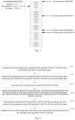
- the specified storage spaces are BLOCKX to BLOCKX+99, and the first two PAGEs, PAGE0 and PAGE1 in BLOCKX have been selected as the first storage spaces, and PAGE2 to PAGE63 in BLOCKX and BLOCKX+1 to BLOCKX+99 have been selected as the second storage spaces, if no valid data storage space has been assigned to any files in the second storage space, the continuous storage space of PAGE2 to PAGE4 in BLOCKX can be assigned to this specified NAND FLASH file as the valid data storage space thereof, specifically refer to File1 shown in Fig. 5 .
- Step 4022 storing the management data of each specified NAND FLASH file in the first storage space, and storing valid data of this specified NAND FLASH file in the valid data storage space assigned for this specified NAND FLASH file.
- the storage location of the management data of each specified NAND FLASH file in the first storage space may be random, or it may be stored in the first storage space in a predetermined order, such as alphabetical order of file names, which is not limited in the present application.
- steps 4021 to 4022 are one possible implementation manner of the step 102 shown in Fig. 1 , and in other possible embodiments, the step 102 shown in Fig. 1 may also be implemented in different implementation manners, which is not limited in the present application.
- Step 403 reading the valid data of the specified NAND FLASH files stored in the second storage space according to the management data of the specified NAND FLASH files stored in the first storage space.
- steps 401 and 403 are the same as steps 101 and 103 shown in Fig. 1 in the implementation principles, respectively, and will not be repeated here.
- the present embodiment assigns the valid data storage space for the specified NAND FLASH file in the first, so that the start position of the management data of the specified NAND FLASH file and the storage position of the valid data of the specified NAND FLASH file are determined accordingly, and the subsequent orderly storage of the management data and valid data of the specified NAND FLASH file may be realized.
- FIG. 6 is a flowchart of the NAND FLASH file data access method in embodiment 4 of the present application. As shown in Fig. 6 , the method includes the following steps:
- steps 601 to 602 are the same as the steps 101 to 102 shown in Fig. 1 in the implementation principle, and will not be described again.
- Step 6031 receiving a file read request for any specified NAND FLASH file.
- the file read request carries the file name of the file to be read.
- Step 6032 reading the management data in the first storage space, searching management data with the same file name as a file name carried by the file read request from the read management data, and determining the found management data as management data of this specified NAND FLASH file.
- all the management data in the first storage space may be read out, and then the file name of the file to be read is searched in the read management data, and the found corresponding management data is the management data of the file to be read.
- Step 6033 determining an end position of this specified NAND FLASH file according to the start position in the management data of this specified NAND FLASH file and the file length.
- the start position in the management data comprises a start block position and a start page position.
- the end position comprises an end block position and an end page position. Since the start block position is used to indicate the block to which the start position belongs, and the start page position is used to indicate the page to which the start position belongs.
- the start block position is referred to as the start block and the start page position is referred to as the start page.
- the end block position is used to indicate the block to which the end position belongs and the end page position is used to indicate the page to which the end position belongs.
- the end block position is referred to as the end block and the end page position is referred to as the end page.
- the end position of the specified NAND FLASH file is determined according to the start position in the management data of this specified NAND FLASH file and file length, and the specific method is as follows: S21, determining the number of PAGEs occupied by the valid data of this specified NAND FLASH file according to the file length of the management data of this specified NAND FLASH file (i.e. the valid data length of this specified NAND FLASH file).
- the number of pages occupied by the valid data of this specified NAND FLASH file may be determined to be 2.
- the start position of this specified NAND FLASH file is PAGE63 of BLOCKX (the start BLOCK, the start PAGE)
- the end position of this specified NAND FLASH file may be determined as BLOCKX+1 (end BLOCK) and PAGE1 (end PAGE) according to the number of pages occupied by the valid data of this specified NAND FLASH file is 2 and the start position of this specified NAND FLASH file.
- Step 6034 reading from the second storage space, data between the start position and the end position of the valid data of this specified NAND FLASH file.
- the start position of the valid data of this specified NAND FLASH file is the start position included in the management data of this specified NAND FLASH file.
- the data read during reading includes the data at the start position and at the end position.
- reading from the second storage space data between the start position and the end position of the valid data of this specified NAND FLASH file specifically includes:
- the start block of the start position is the same as the end block of the end position, which indicates that the start page and the end page of this specified NAND FLASH file are on the same block, and the data from the start page to the end page can be directly read once (continuous multi-page reading).
- the start block of the start position is different from the end block of the end position, indicating that the start page and the end page of the specified NAND FLASH file are not on the same BLOCK, and the valid data of the specified NAND FLASH file is stored across BLOCKs.
- the data needs to be read multiple times. Firstly, performing reading on the valid data on the first BLOCK (i.e., the start BLOCK). Secondly, performing reading on the valid data across several BLOCKs (i.e., respective BLOCKs between the start BLOCK and the end BLOCK, and excluding the start BLOCK and the end BLOCK), and finally performing reading on the valid data on the last block (i.e., the end block).
- the storage of the valid data of this specified NAND FLASH file is as follows: PAGE63 in BLOCKX, PAGE0-PAGE63 in BLOCKX+1 and PAGE0 in BLOCKX+2, that is, the start BLOCK is BLOCKX, the start PAGE is PAGE63, the end BLOCK is BLOCKX+2, and the end PAGE is PAGE0.
- the reading on the valid data of this specified NAND FLASH file may be performed in three times: the first time) reading PAGE63 in BLOCKX, the second time) reading BLOCKX+1 in whole block, and the third time) reading PAGE0 in BLOCKX+2.
- steps 6031 to 6034 are a possible implementation of the step 103 shown in Fig. 1 , and in other possible embodiments, the step 103 shown in Fig. 1 may also be implemented in other ways, which is not limited by the present embodiment.
- the present embodiment determines the end position of this specified NAND FLASH file according to the start position in the management data of this specified NAND FLASH file and file length, so as to quickly locate the storage position of the valid data of this specified NAND FLASH file and performing reading on the valid data block by block, which may further improve the reading speed and reading efficiency of the NAND FLASH file.
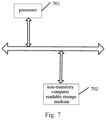
- Fig. 7 is a schematic structural diagram of a device for accessing data of a NAND FLASH file according to an embodiment of the present application.
- the device comprises a processor 701 and a non-transitory computer readable storage medium 702 connected to the processor 701 via a bus.
- the non-transitory computer readable storage medium 702 stores one or more computer programs that may be executed by the processor 701; when executing the one or more computer programs, the processor 701 performs the following steps:
- the processor 701 divides the specified storage space assigned for the specified NAND FLASH files into the first storage space and the second storage space, includes:
- the processor 701 when selecting a continuous storage space of at least M pages from the specified storage space, is configured for: selecting a continuous storage space of at least M pages at the beginning of the specified storage space; or, selecting a continuous storage space of at least M pages in a reverse direction at the end of the specified storage space.
- the processor 701 stores the management data of the specified NAND FLASH files in the first storage space and stores the valid data of the specified NAND FLASH files in the second storage space, includes:
- the management data includes a file name, a start position and a file length
- the processor 701 assigns a valid data storage space in the second storage space for each specified NAND FLASH file, and generates the management data of this specified NAND FLASH file based on the valid data storage space, includes:
- the processor 701 reads the valid data of the specified NAND FLASH file stored in the second storage space according to the management data of the specified NAND FLASH file stored in the first storage space, includes:
- the start position includes a start block and a start page
- An embodiment of the present application also provides a non-transitory computer readable storage medium storing instructions that, when executed by a processor, cause the processor to perform the steps in the method for accessing data of a NAND FLASH file, as shown in the above-mentioned Fig. 1, Fig. 2 , Fig. 4 or Fig. 6 .
- a computer program product containing instructions, which, when run on a computer, causes the computer to perform the steps in the method for accessing data of a NAND FLASH file, as shown in the above-mentioned Fig. 1, Fig. 2 , Fig.4 or Fig.6 .
Landscapes
- Engineering & Computer Science (AREA)
- Theoretical Computer Science (AREA)
- Physics & Mathematics (AREA)
- General Engineering & Computer Science (AREA)
- General Physics & Mathematics (AREA)
- Human Computer Interaction (AREA)
- Information Retrieval, Db Structures And Fs Structures Therefor (AREA)
Applications Claiming Priority (2)
| Application Number | Priority Date | Filing Date | Title |
|---|---|---|---|
| CN202010263561.6A CN113495681B (zh) | 2020-04-07 | 2020-04-07 | 一种nand flash文件数据存取方法、装置及存储介质 |
| PCT/CN2021/082457 WO2021203964A1 (zh) | 2020-04-07 | 2021-03-23 | 一种nand flash文件数据存取方法、装置及存储介质 |
Publications (3)
| Publication Number | Publication Date |
|---|---|
| EP4134802A1 true EP4134802A1 (de) | 2023-02-15 |
| EP4134802A4 EP4134802A4 (de) | 2023-08-30 |
| EP4134802B1 EP4134802B1 (de) | 2025-06-25 |
Family
ID=77995200
Family Applications (1)
| Application Number | Title | Priority Date | Filing Date |
|---|---|---|---|
| EP21785191.4A Active EP4134802B1 (de) | 2020-04-07 | 2021-03-23 | Verfahren und vorrichtung für datenzugriff auf nand-flash-dateien und speichermedium |
Country Status (4)
| Country | Link |
|---|---|
| US (1) | US12182434B2 (de) |
| EP (1) | EP4134802B1 (de) |
| CN (1) | CN113495681B (de) |
| WO (1) | WO2021203964A1 (de) |
Families Citing this family (1)
| Publication number | Priority date | Publication date | Assignee | Title |
|---|---|---|---|---|
| CN114296637B (zh) * | 2021-12-09 | 2024-05-17 | 广西东信数建信息科技有限公司 | 一种本地存储卷动态创建方法及设备 |
Family Cites Families (30)
| Publication number | Priority date | Publication date | Assignee | Title |
|---|---|---|---|---|
| AU2003286967B2 (en) | 2002-12-24 | 2009-01-15 | Lg Electronics, Inc. | Dual journaling store method and storage medium thereof |
| US20060184718A1 (en) * | 2005-02-16 | 2006-08-17 | Sinclair Alan W | Direct file data programming and deletion in flash memories |
| US20070016721A1 (en) * | 2005-07-18 | 2007-01-18 | Wyse Technology Inc. | Flash file system power-up by using sequential sector allocation |
| US7409489B2 (en) * | 2005-08-03 | 2008-08-05 | Sandisk Corporation | Scheduling of reclaim operations in non-volatile memory |
| US20070143566A1 (en) * | 2005-12-21 | 2007-06-21 | Gorobets Sergey A | Non-volatile memories with data alignment in a directly mapped file storage system |
| US20070143560A1 (en) * | 2005-12-21 | 2007-06-21 | Gorobets Sergey A | Non-volatile memories with memory allocation for a directly mapped file storage system |
| US20070156998A1 (en) * | 2005-12-21 | 2007-07-05 | Gorobets Sergey A | Methods for memory allocation in non-volatile memories with a directly mapped file storage system |
| US20070143378A1 (en) * | 2005-12-21 | 2007-06-21 | Gorobets Sergey A | Non-volatile memories with adaptive file handling in a directly mapped file storage system |
| US20070143561A1 (en) * | 2005-12-21 | 2007-06-21 | Gorobets Sergey A | Methods for adaptive file data handling in non-volatile memories with a directly mapped file storage system |
| US20070143567A1 (en) * | 2005-12-21 | 2007-06-21 | Gorobets Sergey A | Methods for data alignment in non-volatile memories with a directly mapped file storage system |
| KR20090102789A (ko) * | 2006-12-06 | 2009-09-30 | 퓨전 멀티시스템즈, 인크.(디비에이 퓨전-아이오) | 프로그레시브 raid를 이용한 데이터 저장 장치, 시스템 및 방법 |
| US8959280B2 (en) * | 2008-06-18 | 2015-02-17 | Super Talent Technology, Corp. | Super-endurance solid-state drive with endurance translation layer (ETL) and diversion of temp files for reduced flash wear |
| KR101515525B1 (ko) | 2008-10-02 | 2015-04-28 | 삼성전자주식회사 | 메모리 장치 및 메모리 장치의 동작 방법 |
| CN101382876A (zh) * | 2008-10-07 | 2009-03-11 | 北京创毅视讯科技有限公司 | 一种数据存储方法 |
| WO2010103760A1 (ja) | 2009-03-13 | 2010-09-16 | パナソニック株式会社 | アクセスモジュール、情報記録モジュール、コントローラ、及び情報記録システム |
| US8930647B1 (en) * | 2011-04-06 | 2015-01-06 | P4tents1, LLC | Multiple class memory systems |
| CN102279805A (zh) * | 2011-09-06 | 2011-12-14 | 四川九洲电器集团有限责任公司 | 一种存储器数据存放及读取方法 |
| US20130080481A1 (en) * | 2011-09-27 | 2013-03-28 | Sybase, Inc. | Extreme large space allocation |
| JP2014179066A (ja) | 2013-02-14 | 2014-09-25 | Panasonic Corp | ストレージ制御装置、ストレージシステム、およびストレージ制御方法 |
| US9009565B1 (en) * | 2013-03-15 | 2015-04-14 | Pmc-Sierra, Inc. | Systems and methods for mapping for solid-state memory |
| CN105335095B (zh) * | 2014-08-11 | 2019-04-05 | 北京兆易创新科技股份有限公司 | 闪存文件系统的处理方法及装置 |
| CN105468642A (zh) * | 2014-09-09 | 2016-04-06 | 杭州海康威视数字技术股份有限公司 | 数据的存储方法及装置 |
| KR101758331B1 (ko) * | 2015-12-22 | 2017-07-31 | 성균관대학교산학협력단 | 비휘발성 메모리 기반의 파일 기록 장치 및 그 방법 |
| JP6523193B2 (ja) * | 2016-03-08 | 2019-05-29 | 東芝メモリ株式会社 | ストレージシステム、情報処理システムおよび制御方法 |
| CN106293532A (zh) * | 2016-08-10 | 2017-01-04 | 广东佳禾声学科技有限公司 | 一种Flash数据储存方法 |
| TWI679534B (zh) * | 2017-09-18 | 2019-12-11 | 慧榮科技股份有限公司 | 資料儲存裝置以及資料儲存方法 |
| CN108089821A (zh) * | 2017-12-20 | 2018-05-29 | 福建星海通信科技有限公司 | 一种微控制器数据存储管理的方法 |
| CN109189772B (zh) * | 2018-08-21 | 2021-09-28 | 华清瑞达(天津)科技有限公司 | 用于无文件系统存储介质的文件管理方法及系统 |
| CN109918234B (zh) * | 2019-03-06 | 2020-07-07 | 苏州浪潮智能科技有限公司 | 一种基于ssd的元数据恢复方法、装置、设备及介质 |
| CN110147203B (zh) * | 2019-05-16 | 2022-11-04 | 北京金山云网络技术有限公司 | 一种文件管理方法、装置、电子设备及存储介质 |
-
2020
- 2020-04-07 CN CN202010263561.6A patent/CN113495681B/zh active Active
-
2021
- 2021-03-23 WO PCT/CN2021/082457 patent/WO2021203964A1/zh not_active Ceased
- 2021-03-23 EP EP21785191.4A patent/EP4134802B1/de active Active
- 2021-03-23 US US17/995,459 patent/US12182434B2/en active Active
Also Published As
| Publication number | Publication date |
|---|---|
| US12182434B2 (en) | 2024-12-31 |
| EP4134802B1 (de) | 2025-06-25 |
| US20230168830A1 (en) | 2023-06-01 |
| WO2021203964A1 (zh) | 2021-10-14 |
| CN113495681B (zh) | 2024-09-24 |
| CN113495681A (zh) | 2021-10-12 |
| EP4134802A4 (de) | 2023-08-30 |
Similar Documents
| Publication | Publication Date | Title |
|---|---|---|
| US11003625B2 (en) | Method and apparatus for operating on file | |
| US11947489B2 (en) | Creating snapshots of a storage volume in a distributed storage system | |
| US8447896B2 (en) | Memory system having high data transfer efficiency and host controller | |
| CN103268201B (zh) | 一种数据存储方法、存储装置及读取方法 | |
| US11314689B2 (en) | Method, apparatus, and computer program product for indexing a file | |
| EP2863310A1 (de) | Datenverarbeitungsverfahren und -vorrichtung sowie vorrichtung für gemeinsame speichernutzung | |
| US9734620B2 (en) | Apparatus and method for graphics state management | |
| CN113568582A (zh) | 数据管理方法、装置和存储设备 | |
| US10083181B2 (en) | Method and system for storing metadata of log-structured file system | |
| CN111190895A (zh) | 列式存储数据的组织方法、装置及存储介质 | |
| CN115964002B (zh) | 一种电能表终端档案管理方法、装置、设备及介质 | |
| CN106201778B (zh) | 信息处理方法及存储设备 | |
| EP4134802B1 (de) | Verfahren und vorrichtung für datenzugriff auf nand-flash-dateien und speichermedium | |
| CN116880780A (zh) | 树的数据写入方法、装置、机器可读介质及存储器 | |
| CN108804571B (zh) | 一种数据存储方法、装置以及设备 | |
| CN118689786B (zh) | 存储芯片的映射表管理方法、电子设备及存储介质 | |
| CN117687704B (zh) | 显卡初始化方法、装置、设备及存储介质 | |
| CN113254271A (zh) | 一种数据序列恢复方法、装置、设备及存储介质 | |
| CN115657950B (zh) | 一种基于多信道的数据读写处理方法、装置及相关设备 | |
| US12353742B2 (en) | Method, device, and computer program product for data deduplication | |
| CN115952177A (zh) | 一种数据库一致性校验方法及装置 | |
| CN114911410A (zh) | 一种数据存储方法、装置、设备及存储介质 | |
| CN119576228B (zh) | 嵌入式设备的文件管理方法及相关装置 | |
| CN115328922B (zh) | 用于单向链表的数据管理方法、装置及系统 | |
| CN118821245B (zh) | 写保护映射方法、装置、计算机可读存储介质及电子设备 |
Legal Events
| Date | Code | Title | Description |
|---|---|---|---|
| STAA | Information on the status of an ep patent application or granted ep patent |
Free format text: STATUS: THE INTERNATIONAL PUBLICATION HAS BEEN MADE |
|
| PUAI | Public reference made under article 153(3) epc to a published international application that has entered the european phase |
Free format text: ORIGINAL CODE: 0009012 |
|
| STAA | Information on the status of an ep patent application or granted ep patent |
Free format text: STATUS: REQUEST FOR EXAMINATION WAS MADE |
|
| 17P | Request for examination filed |
Effective date: 20221010 |
|
| AK | Designated contracting states |
Kind code of ref document: A1 Designated state(s): AL AT BE BG CH CY CZ DE DK EE ES FI FR GB GR HR HU IE IS IT LI LT LU LV MC MK MT NL NO PL PT RO RS SE SI SK SM TR |
|
| DAV | Request for validation of the european patent (deleted) | ||
| DAX | Request for extension of the european patent (deleted) | ||
| A4 | Supplementary search report drawn up and despatched |
Effective date: 20230727 |
|
| RIC1 | Information provided on ipc code assigned before grant |
Ipc: G06F 12/02 20060101ALI20230721BHEP Ipc: G06F 3/06 20060101AFI20230721BHEP |
|
| STAA | Information on the status of an ep patent application or granted ep patent |
Free format text: STATUS: EXAMINATION IS IN PROGRESS |
|
| 17Q | First examination report despatched |
Effective date: 20241119 |
|
| GRAP | Despatch of communication of intention to grant a patent |
Free format text: ORIGINAL CODE: EPIDOSNIGR1 |
|
| STAA | Information on the status of an ep patent application or granted ep patent |
Free format text: STATUS: GRANT OF PATENT IS INTENDED |
|
| INTG | Intention to grant announced |
Effective date: 20250228 |
|
| GRAS | Grant fee paid |
Free format text: ORIGINAL CODE: EPIDOSNIGR3 |
|
| GRAA | (expected) grant |
Free format text: ORIGINAL CODE: 0009210 |
|
| STAA | Information on the status of an ep patent application or granted ep patent |
Free format text: STATUS: THE PATENT HAS BEEN GRANTED |
|
| AK | Designated contracting states |
Kind code of ref document: B1 Designated state(s): AL AT BE BG CH CY CZ DE DK EE ES FI FR GB GR HR HU IE IS IT LI LT LU LV MC MK MT NL NO PL PT RO RS SE SI SK SM TR |
|
| REG | Reference to a national code |
Ref country code: GB Ref legal event code: FG4D |
|
| REG | Reference to a national code |
Ref country code: CH Ref legal event code: EP |
|
| REG | Reference to a national code |
Ref country code: DE Ref legal event code: R096 Ref document number: 602021032953 Country of ref document: DE |
|
| REG | Reference to a national code |
Ref country code: CH Ref legal event code: EP |
|
| REG | Reference to a national code |
Ref country code: IE Ref legal event code: FG4D |
|
| PG25 | Lapsed in a contracting state [announced via postgrant information from national office to epo] |
Ref country code: FI Free format text: LAPSE BECAUSE OF FAILURE TO SUBMIT A TRANSLATION OF THE DESCRIPTION OR TO PAY THE FEE WITHIN THE PRESCRIBED TIME-LIMIT Effective date: 20250625 |
|
| REG | Reference to a national code |
Ref country code: LT Ref legal event code: MG9D |
|
| PG25 | Lapsed in a contracting state [announced via postgrant information from national office to epo] |
Ref country code: NO Free format text: LAPSE BECAUSE OF FAILURE TO SUBMIT A TRANSLATION OF THE DESCRIPTION OR TO PAY THE FEE WITHIN THE PRESCRIBED TIME-LIMIT Effective date: 20250925 Ref country code: GR Free format text: LAPSE BECAUSE OF FAILURE TO SUBMIT A TRANSLATION OF THE DESCRIPTION OR TO PAY THE FEE WITHIN THE PRESCRIBED TIME-LIMIT Effective date: 20250926 |
|
| PG25 | Lapsed in a contracting state [announced via postgrant information from national office to epo] |
Ref country code: BG Free format text: LAPSE BECAUSE OF FAILURE TO SUBMIT A TRANSLATION OF THE DESCRIPTION OR TO PAY THE FEE WITHIN THE PRESCRIBED TIME-LIMIT Effective date: 20250625 |
|
| PG25 | Lapsed in a contracting state [announced via postgrant information from national office to epo] |
Ref country code: HR Free format text: LAPSE BECAUSE OF FAILURE TO SUBMIT A TRANSLATION OF THE DESCRIPTION OR TO PAY THE FEE WITHIN THE PRESCRIBED TIME-LIMIT Effective date: 20250625 |
|
| PG25 | Lapsed in a contracting state [announced via postgrant information from national office to epo] |
Ref country code: RS Free format text: LAPSE BECAUSE OF FAILURE TO SUBMIT A TRANSLATION OF THE DESCRIPTION OR TO PAY THE FEE WITHIN THE PRESCRIBED TIME-LIMIT Effective date: 20250925 |
|
| PG25 | Lapsed in a contracting state [announced via postgrant information from national office to epo] |
Ref country code: LV Free format text: LAPSE BECAUSE OF FAILURE TO SUBMIT A TRANSLATION OF THE DESCRIPTION OR TO PAY THE FEE WITHIN THE PRESCRIBED TIME-LIMIT Effective date: 20250625 |
|
| REG | Reference to a national code |
Ref country code: NL Ref legal event code: MP Effective date: 20250625 |
|
| P01 | Opt-out of the competence of the unified patent court (upc) registered |
Free format text: CASE NUMBER: UPC_APP_8204_4134802/2025 Effective date: 20250929 |
|
| PG25 | Lapsed in a contracting state [announced via postgrant information from national office to epo] |
Ref country code: NL Free format text: LAPSE BECAUSE OF FAILURE TO SUBMIT A TRANSLATION OF THE DESCRIPTION OR TO PAY THE FEE WITHIN THE PRESCRIBED TIME-LIMIT Effective date: 20250625 |
|
| PG25 | Lapsed in a contracting state [announced via postgrant information from national office to epo] |
Ref country code: PT Free format text: LAPSE BECAUSE OF FAILURE TO SUBMIT A TRANSLATION OF THE DESCRIPTION OR TO PAY THE FEE WITHIN THE PRESCRIBED TIME-LIMIT Effective date: 20251027 |
|
| REG | Reference to a national code |
Ref country code: AT Ref legal event code: MK05 Ref document number: 1807162 Country of ref document: AT Kind code of ref document: T Effective date: 20250625 |
|
| PG25 | Lapsed in a contracting state [announced via postgrant information from national office to epo] |
Ref country code: IS Free format text: LAPSE BECAUSE OF FAILURE TO SUBMIT A TRANSLATION OF THE DESCRIPTION OR TO PAY THE FEE WITHIN THE PRESCRIBED TIME-LIMIT Effective date: 20251025 |
|
| PG25 | Lapsed in a contracting state [announced via postgrant information from national office to epo] |
Ref country code: AT Free format text: LAPSE BECAUSE OF FAILURE TO SUBMIT A TRANSLATION OF THE DESCRIPTION OR TO PAY THE FEE WITHIN THE PRESCRIBED TIME-LIMIT Effective date: 20250625 Ref country code: SM Free format text: LAPSE BECAUSE OF FAILURE TO SUBMIT A TRANSLATION OF THE DESCRIPTION OR TO PAY THE FEE WITHIN THE PRESCRIBED TIME-LIMIT Effective date: 20250625 |
|
| PG25 | Lapsed in a contracting state [announced via postgrant information from national office to epo] |
Ref country code: CZ Free format text: LAPSE BECAUSE OF FAILURE TO SUBMIT A TRANSLATION OF THE DESCRIPTION OR TO PAY THE FEE WITHIN THE PRESCRIBED TIME-LIMIT Effective date: 20250625 |
|
| PG25 | Lapsed in a contracting state [announced via postgrant information from national office to epo] |
Ref country code: PL Free format text: LAPSE BECAUSE OF FAILURE TO SUBMIT A TRANSLATION OF THE DESCRIPTION OR TO PAY THE FEE WITHIN THE PRESCRIBED TIME-LIMIT Effective date: 20250625 |
|
| PG25 | Lapsed in a contracting state [announced via postgrant information from national office to epo] |
Ref country code: EE Free format text: LAPSE BECAUSE OF FAILURE TO SUBMIT A TRANSLATION OF THE DESCRIPTION OR TO PAY THE FEE WITHIN THE PRESCRIBED TIME-LIMIT Effective date: 20250625 |
|
| PG25 | Lapsed in a contracting state [announced via postgrant information from national office to epo] |
Ref country code: SK Free format text: LAPSE BECAUSE OF FAILURE TO SUBMIT A TRANSLATION OF THE DESCRIPTION OR TO PAY THE FEE WITHIN THE PRESCRIBED TIME-LIMIT Effective date: 20250625 |
|
| PG25 | Lapsed in a contracting state [announced via postgrant information from national office to epo] |
Ref country code: ES Free format text: LAPSE BECAUSE OF FAILURE TO SUBMIT A TRANSLATION OF THE DESCRIPTION OR TO PAY THE FEE WITHIN THE PRESCRIBED TIME-LIMIT Effective date: 20250625 |
|
| PGFP | Annual fee paid to national office [announced via postgrant information from national office to epo] |
Ref country code: GB Payment date: 20260323 Year of fee payment: 6 |
|
| PG25 | Lapsed in a contracting state [announced via postgrant information from national office to epo] |
Ref country code: DK Free format text: LAPSE BECAUSE OF FAILURE TO SUBMIT A TRANSLATION OF THE DESCRIPTION OR TO PAY THE FEE WITHIN THE PRESCRIBED TIME-LIMIT Effective date: 20250625 |
|
| PGFP | Annual fee paid to national office [announced via postgrant information from national office to epo] |
Ref country code: DE Payment date: 20260313 Year of fee payment: 6 |
|
| PG25 | Lapsed in a contracting state [announced via postgrant information from national office to epo] |
Ref country code: IT Free format text: LAPSE BECAUSE OF FAILURE TO SUBMIT A TRANSLATION OF THE DESCRIPTION OR TO PAY THE FEE WITHIN THE PRESCRIBED TIME-LIMIT Effective date: 20250625 |
|
| PGFP | Annual fee paid to national office [announced via postgrant information from national office to epo] |
Ref country code: FR Payment date: 20260330 Year of fee payment: 6 |
|
| PLBE | No opposition filed within time limit |
Free format text: ORIGINAL CODE: 0009261 |
|
| STAA | Information on the status of an ep patent application or granted ep patent |
Free format text: STATUS: NO OPPOSITION FILED WITHIN TIME LIMIT |
|
| REG | Reference to a national code |
Ref country code: CH Ref legal event code: L10 Free format text: ST27 STATUS EVENT CODE: U-0-0-L10-L00 (AS PROVIDED BY THE NATIONAL OFFICE) Effective date: 20260507 |