EP4134684A1 - Fault detection circuit and detection system - Google Patents
Fault detection circuit and detection system Download PDFInfo
- Publication number
- EP4134684A1 EP4134684A1 EP21785640.0A EP21785640A EP4134684A1 EP 4134684 A1 EP4134684 A1 EP 4134684A1 EP 21785640 A EP21785640 A EP 21785640A EP 4134684 A1 EP4134684 A1 EP 4134684A1
- Authority
- EP
- European Patent Office
- Prior art keywords
- sensor
- fault
- fault detection
- detection circuit
- signal line
- Prior art date
- Legal status (The legal status is an assumption and is not a legal conclusion. Google has not performed a legal analysis and makes no representation as to the accuracy of the status listed.)
- Pending
Links
Images


Classifications
-
- G—PHYSICS
- G01—MEASURING; TESTING
- G01R—MEASURING ELECTRIC VARIABLES; MEASURING MAGNETIC VARIABLES
- G01R31/00—Arrangements for testing electric properties; Arrangements for locating electric faults; Arrangements for electrical testing characterised by what is being tested not provided for elsewhere
- G01R31/50—Testing of electric apparatus, lines, cables or components for short-circuits, continuity, leakage current or incorrect line connections
- G01R31/54—Testing for continuity
-
- G—PHYSICS
- G01—MEASURING; TESTING
- G01D—MEASURING NOT SPECIALLY ADAPTED FOR A SPECIFIC VARIABLE; ARRANGEMENTS FOR MEASURING TWO OR MORE VARIABLES NOT COVERED IN A SINGLE OTHER SUBCLASS; TARIFF METERING APPARATUS; MEASURING OR TESTING NOT OTHERWISE PROVIDED FOR
- G01D3/00—Indicating or recording apparatus with provision for the special purposes referred to in the subgroups
- G01D3/08—Indicating or recording apparatus with provision for the special purposes referred to in the subgroups with provision for safeguarding the apparatus, e.g. against abnormal operation, against breakdown
-
- G—PHYSICS
- G01—MEASURING; TESTING
- G01R—MEASURING ELECTRIC VARIABLES; MEASURING MAGNETIC VARIABLES
- G01R19/00—Arrangements for measuring currents or voltages or for indicating presence or sign thereof
- G01R19/165—Indicating that current or voltage is either above or below a predetermined value or within or outside a predetermined range of values
- G01R19/16566—Circuits and arrangements for comparing voltage or current with one or several thresholds and for indicating the result not covered by subgroups G01R19/16504, G01R19/16528, G01R19/16533
- G01R19/1659—Circuits and arrangements for comparing voltage or current with one or several thresholds and for indicating the result not covered by subgroups G01R19/16504, G01R19/16528, G01R19/16533 to indicate that the value is within or outside a predetermined range of values (window)
-
- G—PHYSICS
- G01—MEASURING; TESTING
- G01R—MEASURING ELECTRIC VARIABLES; MEASURING MAGNETIC VARIABLES
- G01R31/00—Arrangements for testing electric properties; Arrangements for locating electric faults; Arrangements for electrical testing characterised by what is being tested not provided for elsewhere
- G01R31/28—Testing of electronic circuits, e.g. by signal tracer
- G01R31/282—Testing of electronic circuits specially adapted for particular applications not provided for elsewhere
- G01R31/2829—Testing of circuits in sensor or actuator systems
Definitions
- the present invention relates to a fault detection circuit and a detection system.
- Patent Document 1 discloses a disconnection detection circuit that detects a disconnection occurring at an output terminal of a bridge circuit whose intermediate voltage changes in accordance with a physical quantity that is a detection target.
- Patent Document 1 Japanese Patent Application Publication No. 2012-008014
- Patent Document 1 is configured such that when a disconnection occurs at the output terminal, the potential of the output terminal becomes the ground potential (that is, equal to or lower than a reference potential) through a resistor. Therefore, it is difficult to distinguish a disconnection fault from a case where a short circuit to the ground occurs. Therefore, it is difficult for the art of Patent Document 1 to implement various fault detections concerning connections of sensors.
- a fault detection circuit includes a sensor signal line connected to a sensor; a pull-up resistor connected between a power supply voltage and the sensor signal line; and a first comparator having a non-inverting input terminal to which the sensor signal line is connected and an inverting input terminal to which a predetermined upper-limit threshold voltage is input.
- the fault detection circuit is configured to output a first fault detection result signal indicating whether or not a fault concerning a connection of the sensor occurs.
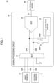
- FIG. 1 is a diagram illustrating a configuration of a detection system 10 according to an embodiment.
- the detection system 10 depicted in FIG. 1 is capable of detecting two different types of detection targets using a first sensor 12 and a second sensor 14. As depicted in FIG. 1 , there are provided the first sensor 12, the second sensor 14, and a signal processing circuit 20.
- the first sensor 12 is a differential-type sensor that outputs differential signals indicating a detection result as a first detection signal.
- the first sensor 12 is connected to the signal processing circuit 20 through two output signal lines 12A and 12B.
- the first sensor 12 outputs the first detection signal (differential signals) indicating a detection result to the signal processing circuit 20 through the two output signal lines 12A and 12B.
- the second sensor 14 is a single-end-type sensor that outputs a single-end-type signal indicating a detection result as a second detection signal.
- the second sensor 14 is connected to the signal processing circuit 20 through a single output signal line 14A.
- the second sensor 14 outputs the second detection signal (single-end-type signal) indicating a detection result to the signal processing circuit 20 through the single output signal line 14A.
- the signal processing circuit 20 is a circuit (so-called AFE (Analog Front End)) that connects the first sensor 12 and the second sensor 14, outputting analog signals, to an external device 60, performing digital signal processing.
- AFE Analog Front End
- the signal processing circuit 20 includes a multiplexer (MUX) 22, an analog-to-digital converter (ADC) 24, and a fault detection circuit 30.
- MUX multiplexer
- ADC analog-to-digital converter
- the input terminals of the multiplexer 22 are connected to the two output signal lines 12A and 12B, connected to the first sensor 12, and the single output signal line 14A, connected to the second sensor 14.
- the multiplexer 22 is connected to two signal lines 23A and 23B which are connected to the analog-to-digital converter 24.
- the multiplexer 22 selectively switches between the first detection signal (the differential signals) output from the first sensor 12 and the second detection signal (single-end-type signal) output from the second sensor 14, and outputs either the first detection signal or the second detection signal to the analog-to-digital converter 24.
- the input terminals of the analog-to-digital converter 24 are connected to two signal lines 23A and 23B connected to the multiplexer 22.
- the output terminal of the analog-to-digital converter 24 is connected to an output signal line 25 that is connected to the external device 60.
- the analog-to-digital converter 24 converts either the first detection signal (the differential signals) or the second detection signal (single-end-type signal) output from the multiplexer 22, from an analog signal to a digital signal; and outputs the digital signal to the external device 60.
- a microcomputer is used as the external device 60, for example.
- the external device 60 is not limited thereto, and any of various processing devices (for example, an IC, a personal computer, a smartphone, a tablet terminal, a server, and the like) that perform digital signal processing may be used as the external device depending on a purpose of use of the detection system 10.
- processing devices for example, an IC, a personal computer, a smartphone, a tablet terminal, a server, and the like
- digital signal processing may be used as the external device depending on a purpose of use of the detection system 10.
- the fault detection circuit 30 detects faults concerning the connections of the first sensor 12 and the second sensor 14.
- the fault detection circuit 30 is connected to the two signal lines 23A and 23B connected to the analog-to-digital converter 24 via two switches 26A and 26B (an example of "switching means").
- the fault detection circuit 30 When the fault detection circuit 30 is to perform fault detection, the fault detection circuit 30 is connected to the two signal lines 23A and 23B as a result of both of the two switches 26A and 26B being turned on.
- the fault detection circuit 30 is not to perform fault detection (that is, when the signal processing circuit 20 is used for routine duties), the fault detection circuit 30 is disconnected from the two signal lines 23A and 23B as a result of both of the two switches 26A and 26B being turned off.
- FIG. 2 is a diagram depicting circuit configurations of the signal processing circuit 20 and the fault detection circuit 30 according to the embodiment.
- the signal processing circuit 20 includes a power supply voltage terminal VDD, four input terminals INP1, INM1, INP2, and INM2, an input terminal EN_MASK, a first multiplexer 31, the fault detection circuit 30, and two output terminals OUT_H and OUT_L.
- the fault detection circuit 30 includes a second multiplexer 32, a sensor signal line 33, a pull-up resistor R1, a first comparator 34, a second comparator 35, and an AND circuit 37.
- the first sensor 12 includes four resistors R2, R3, R4, and R5 forming a bridge circuit.
- the resistors R2 and R4 are connected in series with each other between the power supply voltage terminal VDD and the ground.
- the output signal line 12A is connected to a point where the resistor R2 is connected with the resistor R4.
- the resistors R3 and R5 are connected in series with each other between the power supply voltage VDD and the ground.
- the output signal line 12B is connected to a point where the resistor R3 is connected with the resistor R5.
- the second sensor 14 includes two resistors R6 and R7 connected in series with each other.
- the output signal line 14A is connected to a point where the resistor R6 is connected with the resistor R7.
- One end of the resistor R6 is connected to the power supply voltage VDD, and the other end of the resistor R6 is connected to the resistor R7.
- One end of the resistor R7 is connected to the resistor R6, and the other end of the resistor R7 is connected to the ground.
- input terminals of the first multiplexer 31 are connected to the two output signal lines 12A and 12B that are connected to the first sensor 12.
- an input terminal of the first multiplexer 31 is connected to the single output signal line 14A that is connected to the second sensor 14.
- An input terminal of the first multiplexer 31 is connected to a spare input terminal INM2.
- the first multiplexer 31 selectively switches between the first detection signal (the differential signals) provided from the two signal lines 12A and 12B connected to the first sensor 12 and the second detection signal (the single-end-type signal) provided from the single signal line 14A connected to the second sensor 14, and thus, outputs either the first detection signal or the second detection signal as a signal that is regarded to detect a fault.
- the first multiplexer 31 of the signal processing circuit 20 depicted in FIG. 2 corresponds to the multiplexer 22 depicted in FIG. 1 .
- the two signal lines 31A and 31B of the signal processing circuit 20 depicted in FIG. 2 correspond to the two signal lines 23A and 23B depicted in FIG. 1 .
- another differential-type sensor may be used instead of the second sensor 14.
- two signal lines connected to the other differential-type sensor may be connected to the input terminals INP2 and INM2, and a detection signal (differential signals) may be input from the other differential-type sensor to the fault detection circuit 30 through the two signal lines.
- the input terminals of the second multiplexer 32 are connected to the two output signal lines 31A and 31B that are connected to the output-terminals of the first multiplexer 31.
- the output terminal of the second multiplexer 32 is connected to the sensor signal line 33.
- the second multiplexer 32 selectively switches between the signal provided through the output signal line 31A and the signal provided through the output signal line 31B, and thus, outputs either one of these signals as a signal that is regarded to detect a fault.
- the fault detection circuit 30 can selectively switch between the four signals input from the input terminals INP1, INM1, INP2, and INM2, and thus, provide any one of the four signals to the sensor signal line 33 as a signal that is regarded to detect a fault. That is, the first multiplexer 31 and the second multiplexer 32 are an example of "a selecting means configured to connect any one of a plurality of input terminals, connected to the sensors, to the sensor signal line".
- the first multiplexer 31 outputs the first detection signal (differential signals) as a result of switching and the second multiplexer 32 outputs the signal provided through the signal line 31A as a result of switching, one differential signal of the first detection signal (the differential signals) is provided to the sensor signal line 33.
- the first multiplexer 31 outputs the first detection signal as a result of switching and the second multiplexer 32 outputs the signal provided through the signal line 31A as a result of switching
- the other differential signal of the first detection signal (the differential signals) is provided to the sensor signal line 33.
- the second detection signal (the single-end-type signal) as a result of switching and the second multiplexer 32 outputs the signal provided through the signal line 31A as a result of switching
- the second detection signal (the single-end-type signal) is provided to the sensor signal line 33.
- the spare signal input from the spare input terminal INM2 is provided to the sensor signal line 33.
- one of the four signals input from the four input terminals INP1, INM1, INP2, and INM2 is provided to the sensor signal line 33 as a signal that is regarded to detect a fault.
- the output end of the sensor signal line 33 is connected to the non-inverting terminal (+) of the first comparator 34 and the inverting terminal (-) of the second comparator 35.
- the pull-up resistor R1 is connected between the power supply voltage terminal VDD and the sensor signal line 33.
- the pull-up resistor R1 pulls up the potential of the sensor signal line 33 to a higher potential (a potential higher than a predetermined upper-limit threshold voltage) when a disconnection fault occurs.
- the pull-up resistor R1 has a resistance value (for example, 10 times or more of any one of the resistance values of the resistors R2-R7) sufficiently higher than any one of those of the resistors R2 to R7, so that the potential of the sensor signal line 33 can be increased to be higher than the upper-limit threshold voltage VREFH when any one of faults concerning the connections of the first multiplexer 31 and the second multiplexer 32 occurs, whereas the potential of the sensor signal line 33 is not appreciably affected when any one of faults concerning the connections of the first multiplexer 31 and the second multiplexer 32 does not occur.
- a resistance value for example, 10 times or more of any one of the resistance values of the resistors R2-R7
- the non-inverting terminal (+) of the first comparator 34 is connected to the sensor signal line 33.
- the predetermined upper-limit threshold voltage VREFH is input to the inverting terminal (-) of the first comparator 34.
- the output terminal of the first comparator 34 is connected to the output terminal OUT_H.
- the upper-limit threshold voltage VREFH has a voltage value higher than a predetermined normal voltage range.
- the first comparator 34 When the voltage value of the signal that is regarded to detect a fault, input from the non-inverting terminal (+), is higher than the upper-limit threshold voltage VREFH input from the inverting terminal (-), the first comparator 34 outputs a high-level first fault detection result signal indicating that a fault concerning the connection of the first sensor 12 or the second sensor 14 occurs.
- the first comparator 34 when the voltage value of the signal that is regarded to detect a fault, input from the non-inverting terminal (+), is lower than the upper-limit threshold voltage VREFH input from the inverting terminal (-), the first comparator 34 outputs a low-level first fault detection result signal indicating that a fault concerning the connection of the first sensor 12 or the second sensor 14 does not occur.
- the inverting terminal (-) of the second comparator 35 is connected to the sensor signal line 33.
- a predetermined lower-limit threshold voltage VREFL is input to the non-inverting terminal (+) of the second comparator 35.
- the output terminal of the second comparator 35 is connected to the output terminal OUT_L via the AND circuit 37.
- the lower-limit threshold voltage VREFL has a voltage value lower than the predetermined normal voltage range.
- the second comparator 35 When the voltage value of the signal that is regarded to detect a fault, input from the inverting terminal (-), is lower than the lower-limit threshold voltage VREFL input from the non-inverting terminal (+), the second comparator 35 outputs a high-level second fault detection result signal indicating that a fault concerning the connection of the first sensor 12 or the second sensor 14 occurs.
- the second comparator 35 outputs a low-level second fault detection result signal indicating that a fault concerning the connection of the first sensor 12 or the second sensor 14 does not occur.
- the fault detection circuit 30 when the signal that is regarded to detect a fault is outside the predetermined normal voltage range, the fault detection circuit 30 outputs (for example, to the external device 60 depicted in FIG. 1 ) information indicating that a fault concerning the connection of the sensor (the first sensor 12 or the second sensor 14) that is the output source of the signal that is regarded to detect a fault, by outputting a high-level signal (the high-level first fault detection result signal or the high-level second fault detection result signal) from the first comparator 34 or the second comparator 35.
- a high-level signal the high-level first fault detection result signal or the high-level second fault detection result signal
- the "faults concerning the connections of the sensors" detectable by the fault detection circuit 30 are a disconnection fault (that is, an open-circuit fault) and a short-circuit fault.
- FIG. 3 is a diagram depicting disconnection fault points where faults are detectable by the fault detection circuit 30 according to the embodiment.
- fault points F1 to F10 indicated by bold symbols " ⁇ " are points where the fault detection circuit 30 can detect disconnection faults; and at a time of occurrence of a disconnection fault at any of these points, the voltage value of the sensor signal line 33 is pulled up to a high potential higher than the upper-limit threshold voltage VREFH by the pull-up resistor R1 so that the high-level first fault detection result signal is output from the output terminal OUT_H.
- the potential of the sensor signal line 33 is pulled up to a high potential higher than the upper-limit threshold voltage VREFH by the pull-up resistor R1 when the output signal line 12A is connected to the sensor signal line 33.
- a voltage higher than the upper-limit threshold voltage VREFH is input to the non-inverting terminal (+) of the first comparator 34.
- the first comparator 34 outputs a high-level first fault detection result signal indicating that a disconnection fault occurs on the signal line 12A.
- fault points F11 and F12 indicated by outline symbols " ⁇ " are points where the fault detection circuit 30 can detect disconnection faults; and, at a time of occurrence of a disconnection fault at either one of these points, the voltage value of the sensor signal line 33 becomes "0 V" which is lower than the lower-limit threshold voltage VREFL so that a high-level second detection result signal is output from the output terminal OUT_L.
- V_F 11 VDD ⁇ R 5 / R 1 + R 5
- the pull-up resistor R1 As described above, in the present embodiment, a resistor having a resistance value higher by a factor of ten times or more the resistance value of the resistor R5 is used, for example. Therefore, according to the above formula, when the resistance value of the pull-up resistor R1 is set to a sufficiently high resistance value, the voltage V_F11 of the sensor signal line 33 is substantially 0 V. Thus, the voltage "0 V" lower than the lower-limit threshold voltage VREFL is input to the inverting input terminal (-) of the second comparator 35. As a result, the second comparator 35 outputs a high-level second fault detection result signal indicating that there is a disconnection fault between the resistor R2 and the power supply voltage VDD.
- the fault detection circuit 30 it is possible to freely set a voltage range in which a fault can be detected, by freely adjusting the upper-limit threshold voltage VREFH and the lower-limit threshold voltage VREFL by, for example, setting the resistance values. As a result, in the fault detection circuit 30, it is possible to finely detect a point at which a fault occurs.
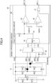
- FIG. 4 is a diagram depicting short-circuit fault points where the fault detection circuit 30 can detect short-circuit faults according to the embodiment.
- fault points F21 and F22 indicated by outline symbols " ⁇ " are points where short-circuit faults can be detected by the fault detection circuit 30. That is, at a time of occurrence of a short-circuit fault with respect to the power supply voltage VDD at any of these points, a high-level first fault detection result signal is output from the output terminal OUT_H. At a time of occurrence of a short-circuit fault with respect to the ground at any of these points, a high-level second fault detection result signal is output from the output terminal OUT_L.
- a fault point F23 indicated by an outline symbol " ⁇ " is a point where the fault detection circuit 30 can detect a short-circuit fault with respect to the power supply voltage VDD; and, at a time of occurrence of a short-circuit fault with respect to the power supply voltage VDD at the point, a high-level fault detection result signal is output from the output terminal OUT_H.
- Fault point F23 the output signal line 14A of the second sensor 14
- the input terminal INM2 when a single-end-type sensor is connected to INP2 and INM2, the input terminal INM2 is in a non-connected state.
- the input of the first multiplexer 31 can be shortcircuited to the ground by switching the switch 36 provided between the input of the first multiplexer 31 and the ground to a turned-on state.
- the input voltage of the first multiplexer 31 is "0 V"
- the input terminal INM2 is regarded to detect a fault
- a high-level second fault detection result signal is output from the second comparator 35. In other words, it would be erroneously determined that a "fault" occurs.
- the second fault detection result signal is input from the second comparator 35 to one input terminal of the AND circuit 37; and an inverted signal of a high-level masking signal, input from the input terminal EN_MASK, is input to the other input terminal of the AND circuit 37, so that masking can be implemented, and thus, a low-level second fault detection result signal can be output from the AND circuit 37 to the output terminal OUT_L.
- the fault detection circuit 30 includes the sensor signal line 33 connected to the sensor; the pull-up resistor R1 connected between the power supply voltage VDD and the sensor signal line 33; and the first comparator 34 having the non-inverting input terminal connected to the sensor signal line 33 and the inverting input terminal to which the predetermined upper-limit threshold voltage VREFH is input. Then, the fault detection circuit 30 according to the embodiment outputs, from the output terminal of the first comparator 34, the first fault detection result signal indicating whether or not a fault concerning the connection of the sensor occurs.
- the fault detection circuit 30 when a fault concerning the connection of the sensor occurs, can pull up the potential of the sensor signal line 33 by the pull-up resistor R1, and can output, from the output terminal of the first comparator 34, the first fault detection result signal indicating that a fault concerning the connection of the sensor occurs.
- the fault detection circuit 30 further includes the second comparator 35 having the inverting input terminal to which the sensor signal line 33 is connected and the non-inverting input terminal to which the predetermined lower-limit threshold voltage VREFL is input.
- the fault detection circuit 30 then outputs the second fault detection result signal, indicating whether or not a fault concerning the connection of the sensor occurs, from the output terminal of the second comparator 35.
- the fault detection circuit 30 can output the second fault detection result signal, indicating that a fault concerning the connection of the sensor occurs, from the output terminal of the second comparator 35.
- the fault detection circuit 30 further includes the first multiplexer 31 and the second multiplexer 32 that connect any one of the plurality of input terminals connected to the sensors to the sensor signal line 33.
- the fault detection circuit 30 can determine whether or not a fault concerning the connection of the sensor occurs, with respect to each of the plurality of signal lines connected to the plurality of input terminals.
- the fault detection circuit 30 has two input terminals per one sensor.
- the two output signal lines of the differential-type sensor can be connected to two input terminals, and also, the single output signal line of the single-end-type sensor can be connected to either one of two input terminals.
- the fault detection circuit 30 can determine whether or not a fault concerning the connection of the sensor occurs, with respect to each of the differential-type sensor and the single-end-type sensor.
- the fault detection circuit 30 is configured to detect faults concerning the connections of the two sensors 12 and 14; but the present invention is not limited thereto, and the configuration of the embodiment may be modified to detect faults concerning the connections of three or more sensors.
- both of fault detection using the comparator 34 and fault detection using the comparator 35 can be performed.
- the present invention is not limited thereto, and for example, the configuration of the embodiment may be modified such that only fault detection using the comparator 34 can be performed without the provision of the comparator 35.
Landscapes
- Physics & Mathematics (AREA)
- General Physics & Mathematics (AREA)
- Testing Of Short-Circuits, Discontinuities, Leakage, Or Incorrect Line Connections (AREA)
Abstract
Description
- The present invention relates to a fault detection circuit and a detection system.
-
Patent Document 1 below discloses a disconnection detection circuit that detects a disconnection occurring at an output terminal of a bridge circuit whose intermediate voltage changes in accordance with a physical quantity that is a detection target. - [Patent Document 1]
Japanese Patent Application Publication No. 2012-008014 - However, the art of
Patent Document 1 is configured such that when a disconnection occurs at the output terminal, the potential of the output terminal becomes the ground potential (that is, equal to or lower than a reference potential) through a resistor. Therefore, it is difficult to distinguish a disconnection fault from a case where a short circuit to the ground occurs. Therefore, it is difficult for the art ofPatent Document 1 to implement various fault detections concerning connections of sensors. - A fault detection circuit according to an embodiment includes a sensor signal line connected to a sensor; a pull-up resistor connected between a power supply voltage and the sensor signal line; and a first comparator having a non-inverting input terminal to which the sensor signal line is connected and an inverting input terminal to which a predetermined upper-limit threshold voltage is input. The fault detection circuit is configured to output a first fault detection result signal indicating whether or not a fault concerning a connection of the sensor occurs.
- In the fault detection circuit of the embodiment, it is easy to implement various fault detections concerning connections of sensors.
-
-
FIG. 1 is a diagram depicting a configuration of a detection system according to an embodiment. -
FIG. 2 is a diagram depicting circuit configurations of a signal processing circuit and a fault detection circuit according to the embodiment. -
FIG. 3 is a diagram depicting points for where disconnection faults can be detected by the fault detection circuit according to the embodiment. -
FIG. 4 is a diagram depicting points for where short-circuit faults can be detected by the fault detection circuit according to the embodiment. - Hereinafter, an embodiment will be described with reference to the drawings.
-
FIG. 1 is a diagram illustrating a configuration of adetection system 10 according to an embodiment. Thedetection system 10 depicted inFIG. 1 is capable of detecting two different types of detection targets using afirst sensor 12 and asecond sensor 14. As depicted inFIG. 1 , there are provided thefirst sensor 12, thesecond sensor 14, and asignal processing circuit 20. - The
first sensor 12 is a differential-type sensor that outputs differential signals indicating a detection result as a first detection signal. Thefirst sensor 12 is connected to thesignal processing circuit 20 through twooutput signal lines first sensor 12 outputs the first detection signal (differential signals) indicating a detection result to thesignal processing circuit 20 through the twooutput signal lines - The
second sensor 14 is a single-end-type sensor that outputs a single-end-type signal indicating a detection result as a second detection signal. Thesecond sensor 14 is connected to thesignal processing circuit 20 through a singleoutput signal line 14A. Thesecond sensor 14 outputs the second detection signal (single-end-type signal) indicating a detection result to thesignal processing circuit 20 through the singleoutput signal line 14A. - The
signal processing circuit 20 is a circuit (so-called AFE (Analog Front End)) that connects thefirst sensor 12 and thesecond sensor 14, outputting analog signals, to anexternal device 60, performing digital signal processing. As depicted inFIG. 1 , thesignal processing circuit 20 includes a multiplexer (MUX) 22, an analog-to-digital converter (ADC) 24, and afault detection circuit 30. - The input terminals of the
multiplexer 22 are connected to the twooutput signal lines first sensor 12, and the singleoutput signal line 14A, connected to thesecond sensor 14. Themultiplexer 22 is connected to twosignal lines digital converter 24. Themultiplexer 22 selectively switches between the first detection signal (the differential signals) output from thefirst sensor 12 and the second detection signal (single-end-type signal) output from thesecond sensor 14, and outputs either the first detection signal or the second detection signal to the analog-to-digital converter 24. - The input terminals of the analog-to-
digital converter 24 are connected to twosignal lines multiplexer 22. The output terminal of the analog-to-digital converter 24 is connected to anoutput signal line 25 that is connected to theexternal device 60. The analog-to-digital converter 24 converts either the first detection signal (the differential signals) or the second detection signal (single-end-type signal) output from themultiplexer 22, from an analog signal to a digital signal; and outputs the digital signal to theexternal device 60. A microcomputer is used as theexternal device 60, for example. However, theexternal device 60 is not limited thereto, and any of various processing devices (for example, an IC, a personal computer, a smartphone, a tablet terminal, a server, and the like) that perform digital signal processing may be used as the external device depending on a purpose of use of thedetection system 10. - The
fault detection circuit 30 detects faults concerning the connections of thefirst sensor 12 and thesecond sensor 14. Thefault detection circuit 30 is connected to the twosignal lines digital converter 24 via twoswitches - When the
fault detection circuit 30 is to perform fault detection, thefault detection circuit 30 is connected to the twosignal lines switches - On the other hand, when the
fault detection circuit 30 is not to perform fault detection (that is, when thesignal processing circuit 20 is used for routine duties), thefault detection circuit 30 is disconnected from the twosignal lines switches - (Circuit Configurations of
Signal Processing Circuit 20 and Fault Detection Circuit 30) -
FIG. 2 is a diagram depicting circuit configurations of thesignal processing circuit 20 and thefault detection circuit 30 according to the embodiment. As depicted inFIG. 2 , thesignal processing circuit 20 includes a power supply voltage terminal VDD, four input terminals INP1, INM1, INP2, and INM2, an input terminal EN_MASK, afirst multiplexer 31, thefault detection circuit 30, and two output terminals OUT_H and OUT_L. - The
fault detection circuit 30 includes asecond multiplexer 32, asensor signal line 33, a pull-up resistor R1, afirst comparator 34, asecond comparator 35, and anAND circuit 37. - As depicted in
FIG. 2 , thefirst sensor 12 includes four resistors R2, R3, R4, and R5 forming a bridge circuit. In thefirst sensor 12, the resistors R2 and R4 are connected in series with each other between the power supply voltage terminal VDD and the ground. In thefirst sensor 12, theoutput signal line 12A is connected to a point where the resistor R2 is connected with the resistor R4. In thefirst sensor 12, the resistors R3 and R5 are connected in series with each other between the power supply voltage VDD and the ground. In thefirst sensor 12, theoutput signal line 12B is connected to a point where the resistor R3 is connected with the resistor R5. - As depicted in
FIG. 2 , thesecond sensor 14 includes two resistors R6 and R7 connected in series with each other. In thesecond sensor 14, theoutput signal line 14A is connected to a point where the resistor R6 is connected with the resistor R7. One end of the resistor R6 is connected to the power supply voltage VDD, and the other end of the resistor R6 is connected to the resistor R7. One end of the resistor R7 is connected to the resistor R6, and the other end of the resistor R7 is connected to the ground. - Through the input terminals INP1 and INM1, input terminals of the
first multiplexer 31 are connected to the twooutput signal lines first sensor 12. Through the input terminal INP2, an input terminal of thefirst multiplexer 31 is connected to the singleoutput signal line 14A that is connected to thesecond sensor 14. An input terminal of thefirst multiplexer 31 is connected to a spare input terminal INM2. Thefirst multiplexer 31 selectively switches between the first detection signal (the differential signals) provided from the twosignal lines first sensor 12 and the second detection signal (the single-end-type signal) provided from thesingle signal line 14A connected to thesecond sensor 14, and thus, outputs either the first detection signal or the second detection signal as a signal that is regarded to detect a fault. Thefirst multiplexer 31 of thesignal processing circuit 20 depicted inFIG. 2 corresponds to themultiplexer 22 depicted inFIG. 1 . The twosignal lines signal processing circuit 20 depicted inFIG. 2 correspond to the twosignal lines FIG. 1 . - In the
detection system 10 of the present embodiment, another differential-type sensor may be used instead of thesecond sensor 14. In this case, in thedetection system 10 according to the present embodiment, two signal lines connected to the other differential-type sensor may be connected to the input terminals INP2 and INM2, and a detection signal (differential signals) may be input from the other differential-type sensor to thefault detection circuit 30 through the two signal lines. - The input terminals of the
second multiplexer 32 are connected to the twooutput signal lines first multiplexer 31. The output terminal of thesecond multiplexer 32 is connected to thesensor signal line 33. Thesecond multiplexer 32 selectively switches between the signal provided through theoutput signal line 31A and the signal provided through theoutput signal line 31B, and thus, outputs either one of these signals as a signal that is regarded to detect a fault. - By thus controlling the
first multiplexer 31 and thesecond multiplexer 32, thefault detection circuit 30 can selectively switch between the four signals input from the input terminals INP1, INM1, INP2, and INM2, and thus, provide any one of the four signals to thesensor signal line 33 as a signal that is regarded to detect a fault. That is, thefirst multiplexer 31 and thesecond multiplexer 32 are an example of "a selecting means configured to connect any one of a plurality of input terminals, connected to the sensors, to the sensor signal line". - For example, when the
first multiplexer 31 outputs the first detection signal (differential signals) as a result of switching and thesecond multiplexer 32 outputs the signal provided through thesignal line 31A as a result of switching, one differential signal of the first detection signal (the differential signals) is provided to thesensor signal line 33. - For example, when the
first multiplexer 31 outputs the first detection signal as a result of switching and thesecond multiplexer 32 outputs the signal provided through thesignal line 31A as a result of switching, the other differential signal of the first detection signal (the differential signals) is provided to thesensor signal line 33. - For example, when the
first multiplexer 31 outputs the second detection signal (the single-end-type signal) as a result of switching and thesecond multiplexer 32 outputs the signal provided through thesignal line 31A as a result of switching, the second detection signal (the single-end-type signal) is provided to thesensor signal line 33. - For example, when the
first multiplexer 31 outputs the second detection signal (the single-end-type signal) as a result of switching and thesecond multiplexer 32 outputs the signal provided through theoutput signal lines 31B as a result of switching, the spare signal input from the spare input terminal INM2 is provided to thesensor signal line 33. - Thus, one of the four signals input from the four input terminals INP1, INM1, INP2, and INM2 is provided to the
sensor signal line 33 as a signal that is regarded to detect a fault. The output end of thesensor signal line 33 is connected to the non-inverting terminal (+) of thefirst comparator 34 and the inverting terminal (-) of thesecond comparator 35. - The pull-up resistor R1 is connected between the power supply voltage terminal VDD and the
sensor signal line 33. The pull-up resistor R1 pulls up the potential of thesensor signal line 33 to a higher potential (a potential higher than a predetermined upper-limit threshold voltage) when a disconnection fault occurs. The pull-up resistor R1 has a resistance value (for example, 10 times or more of any one of the resistance values of the resistors R2-R7) sufficiently higher than any one of those of the resistors R2 to R7, so that the potential of thesensor signal line 33 can be increased to be higher than the upper-limit threshold voltage VREFH when any one of faults concerning the connections of thefirst multiplexer 31 and thesecond multiplexer 32 occurs, whereas the potential of thesensor signal line 33 is not appreciably affected when any one of faults concerning the connections of thefirst multiplexer 31 and thesecond multiplexer 32 does not occur. - The non-inverting terminal (+) of the
first comparator 34 is connected to thesensor signal line 33. The predetermined upper-limit threshold voltage VREFH is input to the inverting terminal (-) of thefirst comparator 34. The output terminal of thefirst comparator 34 is connected to the output terminal OUT_H. The upper-limit threshold voltage VREFH has a voltage value higher than a predetermined normal voltage range. - When the voltage value of the signal that is regarded to detect a fault, input from the non-inverting terminal (+), is higher than the upper-limit threshold voltage VREFH input from the inverting terminal (-), the
first comparator 34 outputs a high-level first fault detection result signal indicating that a fault concerning the connection of thefirst sensor 12 or thesecond sensor 14 occurs. - On the other hand, when the voltage value of the signal that is regarded to detect a fault, input from the non-inverting terminal (+), is lower than the upper-limit threshold voltage VREFH input from the inverting terminal (-), the
first comparator 34 outputs a low-level first fault detection result signal indicating that a fault concerning the connection of thefirst sensor 12 or thesecond sensor 14 does not occur. - The inverting terminal (-) of the
second comparator 35 is connected to thesensor signal line 33. A predetermined lower-limit threshold voltage VREFL is input to the non-inverting terminal (+) of thesecond comparator 35. The output terminal of thesecond comparator 35 is connected to the output terminal OUT_L via the ANDcircuit 37. The lower-limit threshold voltage VREFL has a voltage value lower than the predetermined normal voltage range. - When the voltage value of the signal that is regarded to detect a fault, input from the inverting terminal (-), is lower than the lower-limit threshold voltage VREFL input from the non-inverting terminal (+), the
second comparator 35 outputs a high-level second fault detection result signal indicating that a fault concerning the connection of thefirst sensor 12 or thesecond sensor 14 occurs. - On the other hand, when the voltage value of the signal that is regarded to detect a fault, input from the inverting terminal (-), is higher than the lower-limit threshold voltage VREFL input from the non-inverting terminal (+), the
second comparator 35 outputs a low-level second fault detection result signal indicating that a fault concerning the connection of thefirst sensor 12 or thesecond sensor 14 does not occur. - Thus, when the signal that is regarded to detect a fault is outside the predetermined normal voltage range, the
fault detection circuit 30 outputs (for example, to theexternal device 60 depicted inFIG. 1 ) information indicating that a fault concerning the connection of the sensor (thefirst sensor 12 or the second sensor 14) that is the output source of the signal that is regarded to detect a fault, by outputting a high-level signal (the high-level first fault detection result signal or the high-level second fault detection result signal) from thefirst comparator 34 or thesecond comparator 35. - The "faults concerning the connections of the sensors" detectable by the
fault detection circuit 30 are a disconnection fault (that is, an open-circuit fault) and a short-circuit fault. -
FIG. 3 is a diagram depicting disconnection fault points where faults are detectable by thefault detection circuit 30 according to the embodiment. - In
FIG. 3 , fault points F1 to F10 indicated by bold symbols "×" are points where thefault detection circuit 30 can detect disconnection faults; and at a time of occurrence of a disconnection fault at any of these points, the voltage value of thesensor signal line 33 is pulled up to a high potential higher than the upper-limit threshold voltage VREFH by the pull-up resistor R1 so that the high-level first fault detection result signal is output from the output terminal OUT_H. - Fault point F1: the
output signal line 12A of thefirst sensor 12 - Fault point F2: the
output signal line 12B of thefirst sensor 12 - Fault point F3: the
output signal line 14A of thesecond sensor 14 - Fault point F4: between the resistor R4 and the ground in the
first sensor 12 - Fault point F5: between the resistor R5 and the ground in the
first sensor 12 - Fault point F6: between the resistor R7 and the ground in the
second sensor 14 - Fault point F7: between the
switch 36 and thefirst multiplexer 31 - Fault point F8: the
output signal line 31A of thefirst multiplexer 31 - Fault point F9: the
output signal line 31B of thefirst multiplexer 31 - Fault point F10: the sensor signal line 33 (a portion before the connection point with respect to the pull-up resistor R1)
- For example, in response to an occurrence of a disconnection fault at the fault point F1 on the
output signal line 12A, the potential of thesensor signal line 33 is pulled up to a high potential higher than the upper-limit threshold voltage VREFH by the pull-up resistor R1 when theoutput signal line 12A is connected to thesensor signal line 33. As a result, a voltage higher than the upper-limit threshold voltage VREFH is input to the non-inverting terminal (+) of thefirst comparator 34. Thus, thefirst comparator 34 outputs a high-level first fault detection result signal indicating that a disconnection fault occurs on thesignal line 12A. - In
FIG. 3 , fault points F11 and F12 indicated by outline symbols "×" are points where thefault detection circuit 30 can detect disconnection faults; and, at a time of occurrence of a disconnection fault at either one of these points, the voltage value of thesensor signal line 33 becomes "0 V" which is lower than the lower-limit threshold voltage VREFL so that a high-level second detection result signal is output from the output terminal OUT_L. - Fault point F11: between the resistor R2 and the power supply voltage VDD in the
first sensor 12 - Fault point F12: between the resistor R3 and the power supply voltage VDD in the
first sensor 12 - For example, in response to an occurrence of a disconnection fault at the fault point F11 between the resistor R2 and the power supply voltage VDD, the power supply voltage VDD comes not to be applied to the
first sensor 12, but the power supply voltage VDD continues being applied to thefault detection circuit 30. Therefore, the voltage V_F11 of thesensor signal line 33 at the time of the disconnection fault at the fault point F11 can be expressed by the following formula.

- As described above, in the present embodiment, as the pull-up resistor R1, a resistor having a resistance value higher by a factor of ten times or more the resistance value of the resistor R5 is used, for example. Therefore, according to the above formula, when the resistance value of the pull-up resistor R1 is set to a sufficiently high resistance value, the voltage V_F11 of the
sensor signal line 33 is substantially 0 V. Thus, the voltage "0 V" lower than the lower-limit threshold voltage VREFL is input to the inverting input terminal (-) of thesecond comparator 35. As a result, thesecond comparator 35 outputs a high-level second fault detection result signal indicating that there is a disconnection fault between the resistor R2 and the power supply voltage VDD. - In the
fault detection circuit 30, it is possible to freely set a voltage range in which a fault can be detected, by freely adjusting the upper-limit threshold voltage VREFH and the lower-limit threshold voltage VREFL by, for example, setting the resistance values. As a result, in thefault detection circuit 30, it is possible to finely detect a point at which a fault occurs. -
FIG. 4 is a diagram depicting short-circuit fault points where thefault detection circuit 30 can detect short-circuit faults according to the embodiment. - In
FIG. 4 , fault points F21 and F22 indicated by outline symbols "×" are points where short-circuit faults can be detected by thefault detection circuit 30. That is, at a time of occurrence of a short-circuit fault with respect to the power supply voltage VDD at any of these points, a high-level first fault detection result signal is output from the output terminal OUT_H. At a time of occurrence of a short-circuit fault with respect to the ground at any of these points, a high-level second fault detection result signal is output from the output terminal OUT_L. - Fault point F21: the
output signal line 12A of thefirst sensor 12 - Fault point F22: the
output signal line 12B of thefirst sensor 12 - In
FIG. 4 , a fault point F23 indicated by an outline symbol "×" is a point where thefault detection circuit 30 can detect a short-circuit fault with respect to the power supply voltage VDD; and, at a time of occurrence of a short-circuit fault with respect to the power supply voltage VDD at the point, a high-level fault detection result signal is output from the output terminal OUT_H. - Fault point F23: the
output signal line 14A of thesecond sensor 14 - As depicted in
FIGs. 2 to 4 , when a single-end-type sensor is connected to INP2 and INM2, the input terminal INM2 is in a non-connected state. In this case, the input of thefirst multiplexer 31 can be shortcircuited to the ground by switching theswitch 36 provided between the input of thefirst multiplexer 31 and the ground to a turned-on state. However, in this case, the input voltage of thefirst multiplexer 31 is "0 V", and, therefore, if the input terminal INM2 is regarded to detect a fault, a high-level second fault detection result signal is output from thesecond comparator 35. In other words, it would be erroneously determined that a "fault" occurs. Therefore, in this case, in thefault detection circuit 30, the second fault detection result signal is input from thesecond comparator 35 to one input terminal of the ANDcircuit 37; and an inverted signal of a high-level masking signal, input from the input terminal EN_MASK, is input to the other input terminal of the ANDcircuit 37, so that masking can be implemented, and thus, a low-level second fault detection result signal can be output from the ANDcircuit 37 to the output terminal OUT_L. - Thus, the
fault detection circuit 30 according to the embodiment includes thesensor signal line 33 connected to the sensor; the pull-up resistor R1 connected between the power supply voltage VDD and thesensor signal line 33; and thefirst comparator 34 having the non-inverting input terminal connected to thesensor signal line 33 and the inverting input terminal to which the predetermined upper-limit threshold voltage VREFH is input. Then, thefault detection circuit 30 according to the embodiment outputs, from the output terminal of thefirst comparator 34, the first fault detection result signal indicating whether or not a fault concerning the connection of the sensor occurs. - Accordingly, when a fault concerning the connection of the sensor occurs, the
fault detection circuit 30 according to the embodiment can pull up the potential of thesensor signal line 33 by the pull-up resistor R1, and can output, from the output terminal of thefirst comparator 34, the first fault detection result signal indicating that a fault concerning the connection of the sensor occurs. - The
fault detection circuit 30 according to the embodiment further includes thesecond comparator 35 having the inverting input terminal to which thesensor signal line 33 is connected and the non-inverting input terminal to which the predetermined lower-limit threshold voltage VREFL is input. Thefault detection circuit 30 then outputs the second fault detection result signal, indicating whether or not a fault concerning the connection of the sensor occurs, from the output terminal of thesecond comparator 35. - As a result, when the potential of the
sensor signal line 33 falls below the normal voltage range due to an occurrence of a fault concerning the connection of the sensor, thefault detection circuit 30 according to the embodiment can output the second fault detection result signal, indicating that a fault concerning the connection of the sensor occurs, from the output terminal of thesecond comparator 35. - The
fault detection circuit 30 according to the embodiment further includes thefirst multiplexer 31 and thesecond multiplexer 32 that connect any one of the plurality of input terminals connected to the sensors to thesensor signal line 33. - As a result, the
fault detection circuit 30 according to the embodiment can determine whether or not a fault concerning the connection of the sensor occurs, with respect to each of the plurality of signal lines connected to the plurality of input terminals. - The
fault detection circuit 30 according to the embodiment has two input terminals per one sensor. In thefault detection circuit 30, the two output signal lines of the differential-type sensor can be connected to two input terminals, and also, the single output signal line of the single-end-type sensor can be connected to either one of two input terminals. - As a result, the
fault detection circuit 30 according to the embodiment can determine whether or not a fault concerning the connection of the sensor occurs, with respect to each of the differential-type sensor and the single-end-type sensor. - Although the embodiments of the present invention have been described in detail above, the present invention is not limited to these embodiments, and various modifications or variations can be made within the scope of the present invention claimed in the claims.
- For example, in the embodiment, the
fault detection circuit 30 is configured to detect faults concerning the connections of the twosensors - For example, in the embodiment, both of fault detection using the
comparator 34 and fault detection using thecomparator 35 can be performed. However, the present invention is not limited thereto, and for example, the configuration of the embodiment may be modified such that only fault detection using thecomparator 34 can be performed without the provision of thecomparator 35. - The present International Application claims priority to
Japanese Patent Application No. 2020-070474 filed on April 9, 2020 -
- 10 Detection system
- 12 First sensor
- 12A, 12B Output signal lines
- 14 Second sensor
- 14A Output signal line
- 20 Signal processing circuit
- 22 Multiplexer
- 23A, 23B Signal line
- 24 Analog-to-digital converter
- 26A, 26B Switches (switching means)
- 30 Fault detection circuit
- 31 First multiplexer (selecting means)
- 32 Second multiplexer (selecting means)
- 33 Sensor signal line
- 34 First comparator
- 35 Second comparator
- 36 Switch
- 37 AND circuit (masking means)
- 60 External device
- R1 Pull-up resistor
- INP1, INM1, INP2, INM2, EN_MASK Input terminals
- OUT_H, OUT_L Output terminals
- VDD Power supply voltage terminal
Claims (10)
- A fault detection circuit comprising:a sensor signal line connected to a sensor;a pull-up resistor connected between a power supply voltage and the sensor signal line; anda first comparator having a non-inverting input terminal to which the sensor signal line is connected and an inverting input terminal to which a predetermined upper-limit threshold voltage is input,whereina first fault detection result signal, indicating whether or not a fault concerning connection of the sensor occurs, is output from an output terminal of the first comparator.
- The fault detection circuit as claimed in claim 1,
wherein
the pull-up resistor is configured to increase a potential of the sensor signal line to be higher than the predetermined upper-limit threshold voltage when the fault concerning connection of the sensor occurs. - The fault detection circuit as claimed in claim 2, further comprisinga second comparator having an inverting input terminal to which the sensor signal line is connected and a non-inverting input terminal to which a predetermined lower-limit threshold voltage is input,whereina second fault detection result signal indicating whether or not a fault concerning connection of the sensor occurs is output from an output terminal of the second comparator.
- The fault detection circuit as claimed in claim 3,
wherein
the fault detection circuit is configured to output the first fault detection result signal indicating that the fault concerning connection of the sensor occurs in response to an occurrence of a disconnection fault with respect to the sensor. - The fault detection circuit as claimed in claim 4,
wherein
the fault detection circuit is configured to output the second fault detection result signal indicating that the fault concerning connection of the sensor occurs in response to an occurrence of a short-circuit fault with respect to the sensor. - The fault detection circuit as claimed in claim 5, further comprising
a selecting means configured to connect any one of a plurality of input terminals, connected to the sensor, to the sensor signal line. - The fault detection circuit as claimed in claim 6,
whereintwo input terminals are provided per one sensor, anda connection of two output signal lines of the sensor that is a differential-type sensor to the two input terminals and a connection of a single output signal line of the sensor that is a single-end-type sensor to one of the two input terminals are enabled. - The fault detection circuit as claimed in claim 7, further comprising
a masking means configured to, in response to the other one of the two input terminals being connected to a ground potential by the selecting means inside, mask the second fault detection result signal indicating that the fault occurs with the second fault detection result signal indicating that the fault does not occur. - A detection system, comprising:a sensor;a signal processing circuit configured to perform a predetermined process on an output signal of the sensor; andthe fault detection circuit claimed in any one of claims 1 to 8.
- The detection system as claimed in claim 9, further comprising
a switching means configured to break a connection between the fault detection circuit and the sensor signal line when the signal processing circuit performs the predetermined process, and connect the fault detection circuit to the sensor signal line when the signal processing circuit does not perform the predetermined process.
Applications Claiming Priority (2)
| Application Number | Priority Date | Filing Date | Title |
|---|---|---|---|
| JP2020070474A JP7542982B2 (en) | 2020-04-09 | 2020-04-09 | Fault detection circuit and detection system |
| PCT/JP2021/013490 WO2021205940A1 (en) | 2020-04-09 | 2021-03-30 | Fault detection circuit and detection system |
Publications (2)
| Publication Number | Publication Date |
|---|---|
| EP4134684A1 true EP4134684A1 (en) | 2023-02-15 |
| EP4134684A4 EP4134684A4 (en) | 2023-08-30 |
Family
ID=78023731
Family Applications (1)
| Application Number | Title | Priority Date | Filing Date |
|---|---|---|---|
| EP21785640.0A Pending EP4134684A4 (en) | 2020-04-09 | 2021-03-30 | FAULT DETECTION CIRCUIT AND DETECTION SYSTEM |
Country Status (4)
| Country | Link |
|---|---|
| EP (1) | EP4134684A4 (en) |
| JP (2) | JP7542982B2 (en) |
| CN (1) | CN115362383B (en) |
| WO (1) | WO2021205940A1 (en) |
Families Citing this family (2)
| Publication number | Priority date | Publication date | Assignee | Title |
|---|---|---|---|---|
| CN114200288B (en) * | 2021-12-20 | 2024-03-19 | 上海辰竹仪表有限公司 | Safety input circuit, circuit fault detection system and circuit fault detection method |
| CN114264974B (en) * | 2021-12-24 | 2024-11-08 | 东风汽车有限公司东风日产乘用车公司 | Rapid detection device for sensors and cables |
Family Cites Families (28)
| Publication number | Priority date | Publication date | Assignee | Title |
|---|---|---|---|---|
| EP0051722B1 (en) * | 1980-11-08 | 1984-12-19 | Robert Bosch Gmbh | Battery charging system, especially for motor vehicles |
| JP2932717B2 (en) * | 1991-02-15 | 1999-08-09 | 松下電器産業株式会社 | Temperature detector |
| US5512890A (en) * | 1992-02-19 | 1996-04-30 | Namco Controls Corporation | Sensor connection system |
| JP3373603B2 (en) * | 1992-12-30 | 2003-02-04 | 北陸電気工業株式会社 | Bridge circuit for sensor |
| JPH1019957A (en) * | 1996-07-09 | 1998-01-23 | Bunka Shutter Co Ltd | Disconnection detection device |
| JPH1114691A (en) * | 1997-06-27 | 1999-01-22 | Denso Corp | Sensor disconnection detection device |
| JP2001062637A (en) * | 1999-08-25 | 2001-03-13 | Okuma Corp | Liquid level detection circuit |
| JP4617545B2 (en) * | 1999-10-13 | 2011-01-26 | 株式会社デンソー | Sensor abnormality detection circuit and physical quantity detection device |
| JP2003288963A (en) * | 2002-03-28 | 2003-10-10 | Nissan Motor Co Ltd | Shield connector |
| JP2004286523A (en) | 2003-03-20 | 2004-10-14 | Yazaki Corp | Leakage determination device, leakage determination program, and insulation resistance measurement device |
| JP2005249516A (en) | 2004-03-03 | 2005-09-15 | Toyota Motor Corp | Signal processing circuit and wheel speed signal processing circuit |
| US7196294B2 (en) * | 2005-02-28 | 2007-03-27 | Ridgetop Group, Inc. | Method and resistive bridge circuit for the detection of solder-joint failures in a digital electronic package |
| JP5517777B2 (en) | 2010-06-25 | 2014-06-11 | 日立オートモティブシステムズ株式会社 | System having disconnection detection circuit and disconnection detection means for bridge circuit |
| CN102185295B (en) * | 2011-04-27 | 2014-08-20 | 江苏大学 | Selective short-circuited protection device and method for mine low-voltage power supply system |
| CN203170019U (en) * | 2012-02-10 | 2013-09-04 | 欧格运动有限责任公司 | Flying disc with detachable elastic cushion |
| KR101937839B1 (en) * | 2012-08-29 | 2019-04-10 | 삼성전자 주식회사 | Ear-phone Connecting Interface and Portable Device including the same, and Operating Method thereof |
| JP2015021790A (en) * | 2013-07-17 | 2015-02-02 | Tdk株式会社 | Method and device for detecting fault in bridge circuit |
| US10078104B2 (en) * | 2014-02-06 | 2018-09-18 | Hitachi Automotive Systems, Ltd. | Load drive circuit |
| US9429126B2 (en) * | 2014-06-05 | 2016-08-30 | Caterpillar Inc. | System and method for detecting short-to-ground fault |
| JP6428360B2 (en) * | 2015-02-23 | 2018-11-28 | ミツミ電機株式会社 | Power supply control semiconductor device |
| CN104880143B (en) * | 2015-05-28 | 2017-12-26 | 西北工业大学 | A kind of multi-modal failure detector of bridge-type resistance strain sensor |
| JP6627503B2 (en) * | 2015-12-29 | 2020-01-08 | ティアック株式会社 | Sensor abnormality detection device |
| JP6636860B2 (en) * | 2016-06-02 | 2020-01-29 | 三菱電機エンジニアリング株式会社 | Resistance measurement circuit |
| JP6683152B2 (en) * | 2017-02-23 | 2020-04-15 | 株式会社デンソー | Abnormality diagnosis device |
| JP6622249B2 (en) * | 2017-05-19 | 2019-12-18 | ミネベアミツミ株式会社 | Motor drive control device and motor drive control method |
| US10329150B2 (en) | 2017-06-29 | 2019-06-25 | GM Global Technology Operations LLC | Fuel cell system and method for determining purity level of hydrogen gas provided to an anode side of the fuel cell |
| TWI640777B (en) * | 2017-08-04 | 2018-11-11 | 錞鐿科技股份有限公司 | Electric meter apparatus with light-blinking function |
| JP7135737B2 (en) | 2018-10-31 | 2022-09-13 | 日本製鉄株式会社 | Austenitic hot-rolled steel sheet, manufacturing method thereof, and wear-resistant parts |
-
2020
- 2020-04-09 JP JP2020070474A patent/JP7542982B2/en active Active
-
2021
- 2021-03-30 CN CN202180027511.0A patent/CN115362383B/en active Active
- 2021-03-30 EP EP21785640.0A patent/EP4134684A4/en active Pending
- 2021-03-30 WO PCT/JP2021/013490 patent/WO2021205940A1/en not_active Ceased
-
2024
- 2024-08-20 JP JP2024138476A patent/JP7676644B2/en active Active
Also Published As
| Publication number | Publication date |
|---|---|
| JP7676644B2 (en) | 2025-05-14 |
| WO2021205940A1 (en) | 2021-10-14 |
| JP2024152873A (en) | 2024-10-25 |
| CN115362383B (en) | 2025-10-17 |
| EP4134684A4 (en) | 2023-08-30 |
| JP2021167740A (en) | 2021-10-21 |
| JP7542982B2 (en) | 2024-09-02 |
| CN115362383A (en) | 2022-11-18 |
Similar Documents
| Publication | Publication Date | Title |
|---|---|---|
| CN112398088B (en) | Intelligent electronic switch | |
| JP7676644B2 (en) | Fault Detection Circuit | |
| EP2527854B1 (en) | Systems and methods for determining electrical faults | |
| EP3657187B1 (en) | Fault detection in a low voltage differential signaling (lvds) system | |
| EP2706518B1 (en) | Alarm system loop monitoring | |
| CN106571803B (en) | Over-voltage and under-voltage detection circuit | |
| US7023352B2 (en) | Voltage-detecting method and related circuits | |
| CN110118899B (en) | Method and apparatus for detecting fault conditions and channel imbalances in a differential signal chain | |
| US8756023B2 (en) | Systems and methods for determining electrical ground faults | |
| CN107389994B (en) | Configurable pin multiplexing method and system applied to current sensor chip | |
| CN110907863B (en) | Analog input channel wiring state detection method and system | |
| CN110676804B (en) | Detection circuit and switch module using same | |
| CN115575452A (en) | Liquid inlet detection circuit and electronic equipment | |
| JP2018054361A (en) | Measurement module | |
| JP2001035335A (en) | Relay failure detecting device | |
| US9093961B2 (en) | Operational amplifier | |
| JP6371111B2 (en) | Receiver | |
| CN107678999A (en) | An I2C isolation circuit | |
| TWI832652B (en) | Source measure device | |
| JP2000209090A (en) | A / D converter | |
| CN119471489A (en) | Signal detection circuit and charging pile | |
| CN118884296A (en) | A detection system, system control method and electronic equipment | |
| CN118897221A (en) | Disconnection detection circuit | |
| JPH0287722A (en) | Input circuit for programmable automatic device | |
| CN115903717A (en) | Digital quantity output circuit with disconnection monitoring function, circuit board and monitoring method |
Legal Events
| Date | Code | Title | Description |
|---|---|---|---|
| STAA | Information on the status of an ep patent application or granted ep patent |
Free format text: STATUS: THE INTERNATIONAL PUBLICATION HAS BEEN MADE |
|
| PUAI | Public reference made under article 153(3) epc to a published international application that has entered the european phase |
Free format text: ORIGINAL CODE: 0009012 |
|
| STAA | Information on the status of an ep patent application or granted ep patent |
Free format text: STATUS: REQUEST FOR EXAMINATION WAS MADE |
|
| 17P | Request for examination filed |
Effective date: 20221006 |
|
| AK | Designated contracting states |
Kind code of ref document: A1 Designated state(s): AL AT BE BG CH CY CZ DE DK EE ES FI FR GB GR HR HU IE IS IT LI LT LU LV MC MK MT NL NO PL PT RO RS SE SI SK SM TR |
|
| DAV | Request for validation of the european patent (deleted) | ||
| DAX | Request for extension of the european patent (deleted) | ||
| REG | Reference to a national code |
Ref country code: DE Ref legal event code: R079 Free format text: PREVIOUS MAIN CLASS: G01R0031000000 Ipc: G01R0031540000 Ref country code: DE Ref legal event code: R079 Ref document number: 602021054938 Country of ref document: DE Free format text: PREVIOUS MAIN CLASS: G01R0031000000 Ipc: G01R0031540000 |
|
| A4 | Supplementary search report drawn up and despatched |
Effective date: 20230727 |
|
| RIC1 | Information provided on ipc code assigned before grant |
Ipc: G01R 31/28 20060101ALN20230721BHEP Ipc: G01R 19/165 20060101ALN20230721BHEP Ipc: G01D 3/08 20060101ALI20230721BHEP Ipc: G01R 31/66 20200101ALI20230721BHEP Ipc: G01R 31/58 20200101ALI20230721BHEP Ipc: G01R 31/54 20200101AFI20230721BHEP |
|
| STAA | Information on the status of an ep patent application or granted ep patent |
Free format text: STATUS: EXAMINATION IS IN PROGRESS |
|
| 17Q | First examination report despatched |
Effective date: 20250314 |
|
| GRAP | Despatch of communication of intention to grant a patent |
Free format text: ORIGINAL CODE: EPIDOSNIGR1 |
|
| STAA | Information on the status of an ep patent application or granted ep patent |
Free format text: STATUS: GRANT OF PATENT IS INTENDED |
|
| RIC1 | Information provided on ipc code assigned before grant |
Ipc: G01R 31/54 20200101AFI20260128BHEP Ipc: G01R 31/58 20200101ALI20260128BHEP Ipc: G01R 31/66 20200101ALI20260128BHEP Ipc: G01D 3/08 20060101ALI20260128BHEP Ipc: G01R 19/165 20060101ALN20260128BHEP Ipc: G01R 31/28 20060101ALN20260128BHEP |
|
| INTG | Intention to grant announced |
Effective date: 20260211 |
|
| GRAS | Grant fee paid |
Free format text: ORIGINAL CODE: EPIDOSNIGR3 |
|
| GRAA | (expected) grant |
Free format text: ORIGINAL CODE: 0009210 |
|
| STAA | Information on the status of an ep patent application or granted ep patent |
Free format text: STATUS: THE PATENT HAS BEEN GRANTED |