EP4132701B1 - Saphirmikroreaktoren - Google Patents
Saphirmikroreaktoren Download PDFInfo
- Publication number
- EP4132701B1 EP4132701B1 EP21722965.7A EP21722965A EP4132701B1 EP 4132701 B1 EP4132701 B1 EP 4132701B1 EP 21722965 A EP21722965 A EP 21722965A EP 4132701 B1 EP4132701 B1 EP 4132701B1
- Authority
- EP
- European Patent Office
- Prior art keywords
- wafer
- microreactor
- sapphire
- micro
- equal
- Prior art date
- Legal status (The legal status is an assumption and is not a legal conclusion. Google has not performed a legal analysis and makes no representation as to the accuracy of the status listed.)
- Active
Links
Images



Classifications
-
- B—PERFORMING OPERATIONS; TRANSPORTING
- B01—PHYSICAL OR CHEMICAL PROCESSES OR APPARATUS IN GENERAL
- B01J—CHEMICAL OR PHYSICAL PROCESSES, e.g. CATALYSIS OR COLLOID CHEMISTRY; THEIR RELEVANT APPARATUS
- B01J19/00—Chemical, physical or physico-chemical processes in general; Their relevant apparatus
- B01J19/0093—Microreactors, e.g. miniaturised or microfabricated reactors
-
- B—PERFORMING OPERATIONS; TRANSPORTING
- B01—PHYSICAL OR CHEMICAL PROCESSES OR APPARATUS IN GENERAL
- B01J—CHEMICAL OR PHYSICAL PROCESSES, e.g. CATALYSIS OR COLLOID CHEMISTRY; THEIR RELEVANT APPARATUS
- B01J2219/00—Chemical, physical or physico-chemical processes in general; Their relevant apparatus
- B01J2219/00781—Aspects relating to microreactors
- B01J2219/00783—Laminate assemblies, i.e. the reactor comprising a stack of plates
-
- B—PERFORMING OPERATIONS; TRANSPORTING
- B01—PHYSICAL OR CHEMICAL PROCESSES OR APPARATUS IN GENERAL
- B01J—CHEMICAL OR PHYSICAL PROCESSES, e.g. CATALYSIS OR COLLOID CHEMISTRY; THEIR RELEVANT APPARATUS
- B01J2219/00—Chemical, physical or physico-chemical processes in general; Their relevant apparatus
- B01J2219/00781—Aspects relating to microreactors
- B01J2219/00788—Three-dimensional assemblies, i.e. the reactor comprising a form other than a stack of plates
-
- B—PERFORMING OPERATIONS; TRANSPORTING
- B01—PHYSICAL OR CHEMICAL PROCESSES OR APPARATUS IN GENERAL
- B01J—CHEMICAL OR PHYSICAL PROCESSES, e.g. CATALYSIS OR COLLOID CHEMISTRY; THEIR RELEVANT APPARATUS
- B01J2219/00—Chemical, physical or physico-chemical processes in general; Their relevant apparatus
- B01J2219/00781—Aspects relating to microreactors
- B01J2219/00801—Means to assemble
- B01J2219/00804—Plurality of plates
- B01J2219/00808—Sealing means
-
- B—PERFORMING OPERATIONS; TRANSPORTING
- B01—PHYSICAL OR CHEMICAL PROCESSES OR APPARATUS IN GENERAL
- B01J—CHEMICAL OR PHYSICAL PROCESSES, e.g. CATALYSIS OR COLLOID CHEMISTRY; THEIR RELEVANT APPARATUS
- B01J2219/00—Chemical, physical or physico-chemical processes in general; Their relevant apparatus
- B01J2219/00781—Aspects relating to microreactors
- B01J2219/00819—Materials of construction
-
- B—PERFORMING OPERATIONS; TRANSPORTING
- B01—PHYSICAL OR CHEMICAL PROCESSES OR APPARATUS IN GENERAL
- B01J—CHEMICAL OR PHYSICAL PROCESSES, e.g. CATALYSIS OR COLLOID CHEMISTRY; THEIR RELEVANT APPARATUS
- B01J2219/00—Chemical, physical or physico-chemical processes in general; Their relevant apparatus
- B01J2219/00781—Aspects relating to microreactors
- B01J2219/00819—Materials of construction
- B01J2219/00824—Ceramic
-
- B—PERFORMING OPERATIONS; TRANSPORTING
- B01—PHYSICAL OR CHEMICAL PROCESSES OR APPARATUS IN GENERAL
- B01J—CHEMICAL OR PHYSICAL PROCESSES, e.g. CATALYSIS OR COLLOID CHEMISTRY; THEIR RELEVANT APPARATUS
- B01J2219/00—Chemical, physical or physico-chemical processes in general; Their relevant apparatus
- B01J2219/00781—Aspects relating to microreactors
- B01J2219/00851—Additional features
- B01J2219/00858—Aspects relating to the size of the reactor
- B01J2219/0086—Dimensions of the flow channels
-
- B—PERFORMING OPERATIONS; TRANSPORTING
- B01—PHYSICAL OR CHEMICAL PROCESSES OR APPARATUS IN GENERAL
- B01J—CHEMICAL OR PHYSICAL PROCESSES, e.g. CATALYSIS OR COLLOID CHEMISTRY; THEIR RELEVANT APPARATUS
- B01J2219/00—Chemical, physical or physico-chemical processes in general; Their relevant apparatus
- B01J2219/00781—Aspects relating to microreactors
- B01J2219/00851—Additional features
- B01J2219/00858—Aspects relating to the size of the reactor
- B01J2219/00862—Dimensions of the reaction cavity itself
-
- B—PERFORMING OPERATIONS; TRANSPORTING
- B01—PHYSICAL OR CHEMICAL PROCESSES OR APPARATUS IN GENERAL
- B01J—CHEMICAL OR PHYSICAL PROCESSES, e.g. CATALYSIS OR COLLOID CHEMISTRY; THEIR RELEVANT APPARATUS
- B01J2219/00—Chemical, physical or physico-chemical processes in general; Their relevant apparatus
- B01J2219/00781—Aspects relating to microreactors
- B01J2219/0099—Cleaning
Definitions
- the present invention belongs to the field of microreaction devices and microprocess engineering. These are in particular devices having microchannels (internal chambers of micrometric to submicrometric dimensions) for conducting mixtures and/or chemical or biochemical reactions. More particularly, such devices are optimized to achieve high temperature and pressure constraints (ie 500°C and 500 bar). For observation and analysis purposes, microreaction devices have a wide transparency range in terms of wavelengths.
- the object of the present invention relates to a microfluidic device or microreactor made of sapphire, transparent, preferably in the wavelength range from 150 to 6500 nm, to its manufacturing process and to its use.
- the document US2007278100 in particular discloses an apparatus for controlling the flow rate of a fluid passing through a microflow path, comprising an electrode layer, an electrolyte layer and a conductive polymer membrane in that order, the conductive polymer membrane being exposed to the flow path. microflow, and the flow rate being controlled by supplying an electric current from the electrode layer to the conductive polymer membrane via the electrolyte layer.
- Table 1 below gives examples of limits generally observed in terms of pressure and temperature for known transparent or semi-transparent microreactors: - Microreactor Settings Polymers Glass-glass Silicon-borosilicate Pressure ⁇ 20 bar ⁇ 400 bar ⁇ 400 bar Temperature ⁇ 100°C ⁇ 150°C ⁇ 400°C
- the present invention relates to a microreactor whose operating characteristics in terms of pressure, temperature and chemical compatibility surpass all other types of known microreactor. In terms of temperature, they exceed polymer, silicon-borosilicate and glass-glass microreactors. In addition, its range of in situ analysis covers the ultraviolet to infrared range.
- An object of the invention is thus a transparent sapphire microreactor, preferably in the wavelength range ranging from 150 to 6500 nm.
- An advantage of the microreactor according to the invention is that it consists essentially of sapphire.
- the microreactor according to the invention is made of transparent sapphire, preferably in the wavelength range from 150 to 6500 nm, in which the sapphire is monocrystalline or polycrystalline, preferably monocrystalline such that the plane c is perpendicular to the surface of the microreactor.
- microreactor or "microfluidic device” means a confined on-chip device whose channel dimensions generally range from 1 to 1,000 ⁇ m within which reactive or non-reactive fluids can flow. .
- the numerous microfabrication techniques available today allow varied and complex geometries. Microreactors are used for studies in the field of microprocess engineering, particularly in flow. Microreactors offer numerous advantages compared to conventional reactors, such as the improvement of transfer phenomena (heat, matter, etc.) on small scales depending on the materials used.
- sapphire we mean the crystalline form of alumina (Al 2 O 3 ), which can be monocrystalline or polycrystalline.
- Synthetic sapphire has compatible properties with extreme conditions of high temperatures, high pressures and particularly corrosive chemical environments. Sapphire is surpassed in hardness and scratch resistance only by diamond. Sapphire has a melting point of 2050°C and has excellent thermal conductivity. Its mechanical and corrosion resistance, its dimensional stability, its resistance to extreme pressures and its very high heat resistance make sapphire a material that stands out from advanced materials such as ceramics and glasses.
- the optical properties of sapphire are exceptional: it is transparent to light waves of length between 150 nm (ultraviolet) and 6500 nm (infrared).
- a single crystal or monocrystalline material is a solid material consisting of a single crystal, formed from a single seed.
- a polycrystal or polycrystalline material is made up of a multitude of small crystals of varying size, shape and orientation separated by grain boundaries.
- the sapphire can be monocrystalline or polycrystalline.
- the sapphire is single crystal and the plane c is perpendicular to the surface of the microreactor.
- transparent we mean a property of a material or device which allows light to pass through it in whole or in part. This property depends on the wavelength of the light, the nature of the material and the thickness to be passed through: thus, the glass is transparent in the visible, and it blocks certain ultraviolet rays.
- FIG 1 represents the transmission diagram of a sapphire microreactor according to the invention whose total thickness (i.e. an assembly of two wafers) is 1 mm.
- wafer or “wafer”, we mean a very thin slice or plate of material used as a substrate for microfabrication.
- the wafers are essentially made of sapphire.
- the microreactor according to the invention may comprise a first wafer, a second wafer, at least one of said wafers comprising at least one microchannel.
- the microreactor can be an assembly of several wafers (ie two or more).
- the Figure 5 presents a microreactor comprising a first wafer (1), a second wafer (2), at least one of said wafers comprising at least one microchannel (3).
- the microreactor according to the invention does not include an intermediate layer (for example made of elastomers - Nitrile, Buna-N, Viton or Kalrez), between the wafers, allowing or promoting the assembly of the wafers.
- an intermediate layer for example made of elastomers - Nitrile, Buna-N, Viton or Kalrez
- the microreactor according to the invention consists only of sapphire.
- a sapphire wafer can have a thickness ranging from 200 to 2000 ⁇ m.
- the typical lateral dimensions of a microreactor are generally between 5 mm and several hundred millimeters.
- the microreactor according to the invention can have a total thickness ranging from 400 ⁇ m to 4000 ⁇ m, preferably from 400 ⁇ m to 1000 ⁇ m.
- the dimensions of the microreactor may vary depending on the intended application. For example, for materials synthesis, a microchannel width of 200 ⁇ m is typically used.
- the microreactor according to the invention does not include an intermediate layer (of a material other than sapphire) between the two superimposed wafers.
- the first and the second wafer can have the same or different thickness.
- the first and the second wafer have an identical thickness.
- microchannel means an etched channel, two of whose dimensions are micrometric to submicrometric.
- a microchannel may comprise at least one input and/or at least one output (also called input or output port), etched or drilled in at least one wafer.
- a microchannel can have variable length and shape.
- a microchannel may include one or more patterns.
- a microchannel may for example comprise one or more rectilinear sections and/or comprise one or more boustrophedon, funnel or zigzag patterns or may comprise micro-dots and porous media.
- a microchannel can be branched or unbranched.
- a microchannel can include one or more branches, for example when it includes several inputs and/or several outputs.
- a microchannel is continuous. THE figures 6 , 7 And 8 show examples of microchannel patterns.
- the first and/or the second wafer may comprise at least one microchannel.
- a microchannel can be etched in at least one wafer.
- a microchannel can be etched in one wafer or in a plurality of wafers, preferably etched in one or two wafers.
- the microchannel is formed by etching in a first wafer, then by covering it with the second wafer during assembly of the microreactor.
- the microchannel is formed by etching in each of the first and second wafers, then the two upper and lower parts of the microchannel are joined opposite each other during assembly of the microreactor.
- FIG 2 presents a sectional view of different types of microchannels: microchannels (A) and (C) are etched in two wafers; microchannels (B) and (D) are etched in a single wafer.
- the at least one microchannel can have an average depth ranging from 0.1 to 500 ⁇ m, preferably from 10 to 100 ⁇ m.
- the depth of a microchannel can be variable or constant over the entire length of the microchannel.
- the depth of a microchannel is constant over the entire length of the microchannel.
- a microchannel depth H is defined.
- the depth H can be identical or different in the two wafers.
- the figure 2 shows a microchannel (A) etched with a greater depth in the wafer (1) than in the wafer (2).
- the at least one microchannel can have a width ranging from 0.1 to 2000 ⁇ m, preferably from 100 to 400 ⁇ m.
- the width of the microchannel can be variable or constant over the entire length of the microchannel.
- the width of a microchannel is constant over the entire length of the microchannel.
- a microchannel can have a greater width Wp and a lower width Ws between the upper and lower part of the engraving.
- the widths Wp and Ws can be identical as on the Figure 4 (for example in the context of plasma engraving) or different as on the Figure 3 (for example in the context of chemical etching).
- the thickness of the wafer/depth of the microchannel ratio can be greater than or equal to 2, preferably greater than or equal to 4.
- the microreactor according to the invention is configured so that the total surface area developed by all of the microchannel(s) is generally less than or equal to half of the total surface area of the wafer.
- the minimum distance between two microchannels, or between two parts of the same microchannel can be greater than or equal to the width of said microchannel.
- the minimum distance between a microchannel and the end of a wafer can be greater than or equal to the width of said microchannel.
- the microreactor according to the invention can comprise a wafer (1) of thickness t p and a wafer (2) of thickness t s , said wafer (2) comprising at least one microchannel (3).
- the microchannel (3) can be characterized by a depth H and a width W.
- the minimum distance Z 1 between two microchannels (3) can be greater than W, preferably greater than 2*W.
- the distance Z 1 is greater than the greater of the two: if W p > W s then Z 1 > W p , preferably Z 1 > 2*W p ; if W s > W p then Z 1 > W s , preferably Z 1 > 2*W s .
- the minimum distance Z 2 between a microchannel (3) and the end of a wafer can be greater than W, preferably greater than 2*W.
- the distance Z 2 is greater than the greater of the two: if W p > W s then Z 2 > W p , preferably Z 2 > 2*W p ; if W s > W p then Z 2 > W s , preferably Z 2 > 2*W s .
- the microreactor according to the invention can have a volume of less than 500 ⁇ l, preferably ranging from 0.5 to 500 ⁇ l.
- the volume of the microreactor means the total volume constituted by all the microchannels included in the microreactor.
- the volume of the microreactor may vary depending on the intended application.
- the microreactor can have a volume ranging from 10 to 500 ⁇ l when it is intended to be used in chemical or materials synthesis.
- the microreactor can have a volume ranging from 0.5 to 10 ⁇ l when it is intended to be used in thermo-hydrogeology.
- the microreactor can have a volume ranging from 0.5 to 500 ⁇ l when it is intended to be used in microbiology in extreme conditions.
- the invention also relates to the use of sapphire for the manufacture of a microreactor.
- step 1) of etching the microchannel can be implemented by any technique known to those skilled in the art.
- step 1) of the method according to the invention can be carried out by a method of photolithography followed by etching (chemical or plasma).
- step 1) of the method according to the invention can be carried out by a direct writing method, laser or machining.
- layer of sacrificial material is meant a thin layer deposited on the surface of the sapphire wafer, which serves as protection and masking during the processing step. engraving.
- this consists of a layer of silicon oxide with a thickness ranging from 300 to 500 nm.
- step b) of chemical etching of the process according to the invention may comprise etching using a solution allowing the elimination of the sacrificial layer present on the wafer.
- step c) of removing the residual resin layer can be done using a solvent (e.g. acetone).
- a solvent e.g. acetone
- step d) of chemical etching of the process according to the invention may comprise etching the wafer with a solution of sulfuric and phosphoric acid (ratio ranging from 3/1 to 4/1 by volume).
- the method according to the invention may further comprise a step of eliminating the residual sacrificial layer, by chemical etching (e.g. use of a hydrofluoric acid solution).
- the method according to the invention may further comprise a step of drilling the input and/or output ports of the wafer(s).
- the assembly of step 2) of the method according to the invention may include a pre-gluing step.
- the pre-gluing step may comprise at least one step of cleaning the wafers followed by pre-gluing in an aqueous solution then by heat treatment in a press system (and preferably under primary vacuum, i.e. 10 to 100 mbar). Cleaning can be carried out for example with a solution of sulfuric acid (H 2 SO 4 ) and hydrogen peroxide (H 2 O 2 ), (4:1, v/v), followed by rinsing (for example in ultra-pure water at a temperature greater than or equal to 60° C. and treatment in a phosphoric acid crystallizer at a temperature greater than or equal to 150° C.
- the pre-gluing of the wafers can then be carried out in a crystallizer.
- the pre-gluing of the wafers can consist of placing the wafers in contact with each other, the engraved face(s) on the interior side, the assembly thus constituted then undergoing a heat treatment at a temperature ranging from 200 to 300° C and for a period of 2 to 4 hours in a press system (screw tightening), preferably under primary vacuum (i.e. 10 to 100 mbar).
- the pre-gluing of the wafers is carried out in a clean room.
- the wafers are brought into contact in an enclosure, compressed via a press (between 2 and 20 bar pressure), brought to temperature (from 200 to 300 °C) then, preferably placed under primary vacuum (10-100 mbar ) for the duration of pre-gluing, using a vacuum pump.
- step 2) of assembly of the method according to the invention can be carried out by any known methods. It can in particular be carried out by Spark Plasma Sintering (SPS), also called Field Activated Sintering Technique (FAST).
- SPS Spark Plasma Sintering
- FAST Field Activated Sintering Technique
- the invention also relates to the use of a microreactor according to the invention for the implementation of fluids at high pressure and/or high temperatures, chemically aggressive fluids (acids, super acids, bases or any fluid corrosive) and supercritical fluids in the fields of synthetic chemistry, thermo-hydrogeology, geochemistry, microbiology in extreme conditions (T ⁇ 1000°C, p ⁇ 2000 bar), preferably at temperatures less than or equal to 500°C and/or pressures less than or equal to 500 bar.
- FIG. 1 represents the transmission diagram of a sapphire microreactor according to the invention whose total thickness is 1 mm (transmission in% as a function of the wavelength ⁇ in ⁇ m).
- FIG. 2 shows a cross-sectional view of microchannels etched in two wafers (A and C) and microchannels etched in a single wafer (B and D).
- FIG. 3 represents a cross-sectional view of a wafer comprising a chemically etched microchannel.
- FIG. 4 represents a sectional view of a wafer comprising a plasma-etched microchannel.
- FIG. 5 represents a sectional view of a microreactor according to the invention comprising a first wafer (1), a second wafer (2) and a microchannel (3).
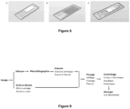
- Pattern (A) represents a “porous medium” type microreactor composed of micro-dots with different diameters. Pattern (A) has an inlet E1 and an outlet S 1 as well as two ports P1 and P2 allowing the pressure upstream and downstream of the micro-plots to be measured. Pattern (B) represents a “segmented flow” type microreactor composed of two inputs E' 1 and E'2 and an output S' 1. The two microchannels connected to the inputs E' 1 and E'2 join together to form only one which continues in order to have a certain channel length until the output S' 1.
- FIG. 7 represents (A) the microreactor C obtained in Example 1 with pattern A of the Figure 4 of porous medium type and (B) a microreactor with pattern B of the figure 4 segmented flow type (alternations of fluids).
- FIG 8 represents in 3D modeling, two patterns (A and C) of microreactor of porous medium type with (A) a uniform porous medium (identical diameter of the micro-dots) and (C) a porous medium composed of micro-dots having three different diameters .
- There figure 8 represents in 3D modeling a segmented flow pattern (B).
- FIG. 9 schematically represents the main stages of manufacturing a microreactor according to the invention.
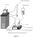
- FIG. 10 represents the device set up for chemical etching.
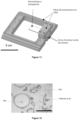
- FIG. 11 represents an injection system, also called a compression part, which allows the inputs and outputs of the microreactor to be connected to reagents. This injection system keeps the microreactor under pressure.
- FIG. 12 represents a photograph taken by optical microscopy (x40 objective) of the interior of an all-sapphire microreactor under pressure during a reaction between water, iron particles and a gas.
- FIG. 13 represents in (A) the image obtained by optical microscopy (x15 objective) during an in situ analysis by infrared spectroscopy of a microreactor filled with a water/pentane/air mixture; in (B) the absorption spectrum of the all-sapphire microreactor used as a background for the in situ analyses; in (C) and (D) respectively the absorption spectra of pentane and water obtained by infrared spectroscopy on the microreactor.
- FIG. 14 represents a mask produced on AUTOCAD software (registered trademark) containing the image of interest or design to be burned into the wafer.
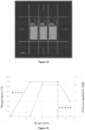
- FIG. 15 represents the parameters used during the assembly step by “Spark Plasma Sintering”, specifically the temperature and pressure ramps applied as a function of time.
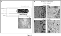
- FIG. 16 represents: (A) a sapphire microreactor pattern which has an inlet and an outlet as well as two ports P1 and P2 allowing the pressure to be measured in upstream and downstream of the micro-studs, said pattern simulating a heterogeneous porous medium with studs of different sizes (25 to 300 ⁇ m) as well as preferential passage zones simulating cracks. (B) visible light images at different growth times (0 and 8 hours) of microorganisms of the Thermococcus Barophilus strain which were cultivated at pressure (100 bar)/temperature (85°C) in a microreactor having the design of the Figure 16-A . It is possible to follow the evolution of microbial development in real time.
- Example 1 Manufacturing of a sapphire microreactor according to the invention
- the pattern of a microchannel (previously drawn on a mask using AUTOCAD software (registered trademark), see Figure 14 ) is printed on the sapphire wafer by the photolithography process.
- This step preferably takes place in a clean room (clean room according to ISO 14644-1).
- the lithography process begins with the uniform application of a few ⁇ m thick film of photosensitive resin (advantageously: 4 ⁇ m), onto the substrate via the use of a spin coating device.
- a cooking step on a hot plate follows the resin deposition (the temperature and duration must be adapted depending on the resin, in this example the cooking was 5 minutes at 115°C).
- the resin is exposed for 45 seconds to ultraviolet rays in an exposing aligner (for example UV-KUB KLOE type).
- an exposing aligner for example UV-KUB KLOE type.
- the wafer is then immersed in a bath of chemical developer including a diluted solution of tetramethylammonium hydroxide which eliminates the exposed areas. These areas are no longer protected by the resin and will therefore be sensitive to etching. To stop the development of the resin, the wafer is then rinsed with water and dried before being heated for a few minutes on a hot plate (around 6 minutes at 115°C).
- the oxide layer, exposed after irradiation of the resin, is removed by acid attack.
- the wafer is placed, side to be etched upwards, in a Teflon crystallizer and the area to be etched is covered with a solution of hydrofluoric acid (HF) buffered at 1% in water, for 7 minutes.
- HF hydrofluoric acid
- the sapphire is engraved.
- the engraving is done with sulfuric (H 2 SO 4 ) and phosphoric (H 3 PO 4 ) acid in the proportions 4 to 1 (v/v), following the assembly presented in Figure 10 .
- the temperature of the mixture stabilizes between 250 and 300°C.
- the entry and exit ports of the wafer are drilled for example using a laser or by using diamond bits.
- a final HF bath (7 min) is carried out to remove the residual oxide layer.
- the wafer pre-gluing step is carried out in clean conditions (clean room) in order to prevent any dust or impurities from getting between the two wafers and compromising the assembly.
- the two wafers, wafer A and a wafer B (preferably of identical lateral dimensions to wafer A) are cleaned with a solution of Piranha (sulfuric acid (H 2 SO 4 ) and hydrogen peroxide (H 2 O 2 , 4 :1 v/v) for 15 min.
- the two wafers are placed for 5 min in ultra-pure water heated to 60°C then transferred to a phosphoric acid crystallizer heated to 150°C.
- the two wafers are placed in a dilute solution of sulfuric acid having a pH of 1 for 5 minutes.
- the wafers are then placed in a crystallizer containing ultra-pure water for 5 minutes.
- the two wafers are then assembled against each other, with the face(s) etched on the inside.
- the assembly thus constituted then undergoes a heat treatment at 200°C for 2 hours in a press system (screw tightening).
- the assembly of the wafers is carried out using the Spark Plasma Sintering (SPS) technique, also called Field Activated Sintering Technique (FAST).
- SPS Spark Plasma Sintering
- FAST Field Activated Sintering Technique
- microreactor is cut by a diamond saw to obtain microreactor C, depending on the dimensions of the pattern and the intended application for the thickness.
- Example 2 Example of use of microreactor C of Example 1 in severe conditions, pressure and temperature test and in situ analysis
- the microreactor of Example 1 is used for microbiology in extreme conditions.
- Microreactor C of Example 1 is connected to a fluid injection system adapted for high pressure and high temperature conditions.
- FIG 11 represents the three-dimensional drawing of the PEEK (polyetheretherketone) compression part developed for these microreactors.
- Microreactor C has a pressure resistance of 400 bar under the conditions relating to the example.
- microreactor C To test microreactor C in temperature, it undergoes a local temperature gradient: 400°C at one end and 11.3°C at the other. After several hours subjected to this temperature gradient, the microreactor remained intact (no cracks, breakages or other changes).
- microreactor according to the invention can withstand the severe conditions according to the example of the temperature and pressure tests described above.
- the microreactor C is transparent over a very wide wavelength range: from infrared to ultraviolet.
- Figure 1 represents a transmission spectrum of a sapphire microreactor as a function of wavelength. This characteristic makes it possible to carry out observations or analyzes ( Figure 13 ) with for example an optical microscope or an infrared spectrometer.
- the Figure 12 shows an image obtained by optical microscopy of the interior of a microreactor (pattern with micro-dots) housing a reaction between water, CO 2(g) and iron particles.
- a reaction between water, CO 2(g) and iron particles can be identified by infrared spectroscopy.
- Example 3 Example of use of a sapphire microreactor for monitoring the growth of extremophilic microbial strains in situ and in real time
- the microreactor was used for the study and cultivation of living microorganisms in extreme conditions, in particular microorganisms from deep ocean environments ( ie Thermococcus barophilus ) .
- the microreactor is filled with a culture medium inoculated with the strain to be studied. The latter is then pressurized and placed in the temperature conditions allowing the development of microorganisms using a heating element in direct contact with the microreactor.
- the microreactor is placed under a confocal microscope to perform in situ and real-time imaging to monitor the growth of microorganisms.
Landscapes
- Chemical & Material Sciences (AREA)
- Organic Chemistry (AREA)
- Chemical Kinetics & Catalysis (AREA)
- Physical Or Chemical Processes And Apparatus (AREA)
- Micromachines (AREA)
- Organic Low-Molecular-Weight Compounds And Preparation Thereof (AREA)
Claims (16)
- Mikroreaktor, der im Wesentlichen aus Saphir, aus transparentem Saphir, bevorzugt im Wellenlängenbereich von 150 bis 6500 nm, besteht, wobei der Saphir monokristallin oder polykristallin, bevorzugt monokristallin ist, derart, dass die Ebene c zur Oberfläche des Mikroreaktors senkrecht ist.
- Mikroreaktor nach Anspruch 1, der einen ersten Wafer (1), einen zweiten Wafer (2) umfasst, wobei mindestens einer der Wafer mindestens einen Mikrokanal (3) umfasst.
- Mikroreaktor nach Anspruch 1 oder 2, wobei der Mikrokanal (3) eine durchschnittliche Tiefe H von 0,1 bis 500 µm aufweist.
- Mikroreaktor nach Anspruch 3, wobei der Mikrokanal (3) eine durchschnittliche Breite W von 0,1 bis 1000 µm aufweist.
- Mikroreaktor nach einem der Ansprüche 2 bis 4, wobei das Verhältnis Dicke des Wafers (2) / Tiefe des Mikrokanals (3) größer oder gleich 2, bevorzugt größer oder gleich 4, ist.
- Mikroreaktor nach Anspruch 4 oder 5, wobei die Gesamtfläche des mindestens einen Mikrokanals kleiner oder gleich der Hälfte der Gesamtfläche des Wafers ist, und bevorzugt der minimale Abstand Z zwischen zwei Mikrokanälen oder zwischen zwei Teilen desselben Mikrokanals größer oder gleich W ist und bevorzugt größer als 2*W ist.
- Mikroreaktor nach einem der vorstehenden Ansprüche, der ein Volumen von kleiner als 500 µl, bevorzugt von 0,5 bis 500 µl, aufweist.
- Verwendung von Saphir zur Herstellung eines Mikroreaktors nach einem der vorstehenden Ansprüche, wobei der Saphir monokristallin oder polykristallin ist.
- Verfahren zur Herstellung eines Mikroreaktors aus Saphir nach einem der Ansprüche 1 bis 7, das die folgenden Schritte umfasst:1) Ätzen mindestens eines Mikrokanals auf mindestens einem Wafer, bevorzugt durch Fotolithographieverfahren, gefolgt von chemischem oder Plasma-Ätzen, oder durch direktes Laser-Schreibverfahren oder Bearbeitung,2) Anbringen des in Schritt 1) erhaltenen geätzten Wafers auf einem geätzten oder ungeätzten zweiten Wafer.
- Verfahren nach dem vorstehenden Anspruch, wobei der Schritt des Ätzens 1) die folgenden Teilschritte umfasst:a) Drucken eines Bildes von Interesse mittels eines Harzes auf mindestens einen Wafer, wobei der Wafer mit einer Opfermaterialschicht bedeckt ist,b) chemisches Ätzen der auf dem Wafer vorhandenen Opfermaterialschicht,c) Entfernen der restlichen Harzschicht,d) chemisches Ätzen der Mikrokanäle gemäß der gewünschten Endtiefe.
- Verfahren nach einem der Ansprüche 9 bis 10, das weiter einen Schritt des Bohrens der Eingangs- und/oder Ausgangsanschlüsse des Wafers oder der Wafer umfasst.
- Verfahren nach einem der Ansprüche 9 bis 11, wobei das Anbringen aus Schritt 2) einen Schritt des Vorverklebens umfasst, wobei der Schritt des Vorverklebens bevorzugt mindestens einen Schritt des Reinigens der Wafer, gefolgt von einem Vorverkleben in wässriger Lösung und anschließend einer Wärmebehandlung in einem System unter Presse und bevorzugt unter Primärvakuum umfasst.
- Verfahren nach dem vorstehenden Anspruch, wobei das Reinigen mittels einer Lösung aus Schwefelsäure (H2SO4) und Wasserstoffperoxid (H2O2), (4:1, v/v), bevorzugt gefolgt von einem Spülen mit Reinstwasser bei einer Temperatur von größer oder gleich 60 °C und einer Behandlung in einem Phosphorsäurekristallisator bei einer Temperatur von größer oder gleich 150 °C ausgeführt wird.
- Verfahren nach Anspruch 12 oder 13, wobei das Vorverkleben im Inkontaktbringen der Wafer miteinander, die geätzte(n) Seite(n) nach innen gewandt, besteht, wobei die so gebildete Anordnung anschließend eine Wärmebehandlung bei einer Temperatur von 200 bis 300 °C und während einer Dauer von 2 bis 4 Stunden in einem System unter Presse und bevorzugt unter Primärvakuum durchläuft.
- Verfahren nach einem der Ansprüche 9 bis 14, wobei das Anbringen aus Schritt 2) nach dem Spark Plasma Sintering- (SPS-) oder Field Activated Sintering Technique- (FAST-) Verfahren ausgeführt wird.
- Verwendung eines Mikroreaktors nach einem der Ansprüche 1 bis 7 für den Einsatz von Hochdruck- und/oder Hochtemperaturfluiden, chemisch aggressiven Fluiden, überkritischen Fluiden im Bereich der Synthesechemie, Thermo-Hydrogeologie, Geochemie, Mikrobiologie unter Extrembedingungen, bevorzugt bei Temperaturen von kleiner oder gleich 500 °C und/oder Drücken von kleiner oder gleich 500 Bar.
Applications Claiming Priority (2)
| Application Number | Priority Date | Filing Date | Title |
|---|---|---|---|
| FR2003453A FR3108860B1 (fr) | 2020-04-07 | 2020-04-07 | Microreacteurs en saphir |
| PCT/FR2021/050604 WO2021205115A1 (fr) | 2020-04-07 | 2021-04-07 | Microréacteurs en saphir |
Publications (2)
| Publication Number | Publication Date |
|---|---|
| EP4132701A1 EP4132701A1 (de) | 2023-02-15 |
| EP4132701B1 true EP4132701B1 (de) | 2024-04-03 |
Family
ID=71784198
Family Applications (1)
| Application Number | Title | Priority Date | Filing Date |
|---|---|---|---|
| EP21722965.7A Active EP4132701B1 (de) | 2020-04-07 | 2021-04-07 | Saphirmikroreaktoren |
Country Status (4)
| Country | Link |
|---|---|
| US (1) | US20230133449A1 (de) |
| EP (1) | EP4132701B1 (de) |
| FR (1) | FR3108860B1 (de) |
| WO (1) | WO2021205115A1 (de) |
Family Cites Families (4)
| Publication number | Priority date | Publication date | Assignee | Title |
|---|---|---|---|---|
| US20040043506A1 (en) * | 2002-08-30 | 2004-03-04 | Horst Haussecker | Cascaded hydrodynamic focusing in microfluidic channels |
| GB0426766D0 (en) * | 2004-12-06 | 2005-01-12 | Q Chip Ltd | Device for fluid transport |
| US20070278100A1 (en) * | 2006-05-30 | 2007-12-06 | Honda Motor Co., Ltd. | Apparatus for controlling flow rate in micro-flow path, microchip apparatus comprising flow-rate-controlling apparatus, and flow-rate-controlling method |
| US8216526B2 (en) * | 2008-06-17 | 2012-07-10 | The United States of America, as represented by the Secretary of Commerce, The National Institute of Standards and Technology | Method and device for generating diffusive gradients in a microfluidic chamber |
-
2020
- 2020-04-07 FR FR2003453A patent/FR3108860B1/fr not_active Expired - Fee Related
-
2021
- 2021-04-07 EP EP21722965.7A patent/EP4132701B1/de active Active
- 2021-04-07 US US17/995,688 patent/US20230133449A1/en active Pending
- 2021-04-07 WO PCT/FR2021/050604 patent/WO2021205115A1/fr not_active Ceased
Also Published As
| Publication number | Publication date |
|---|---|
| EP4132701A1 (de) | 2023-02-15 |
| FR3108860A1 (fr) | 2021-10-08 |
| US20230133449A1 (en) | 2023-05-04 |
| WO2021205115A1 (fr) | 2021-10-14 |
| FR3108860B1 (fr) | 2023-04-21 |
Similar Documents
| Publication | Publication Date | Title |
|---|---|---|
| US7803451B2 (en) | Optical composites between similar and between dissimilar materials | |
| Grogan et al. | The nanoaquarium: a platform for in situ transmission electron microscopy in liquid media | |
| US11069822B2 (en) | Transition metal chalcogenide van der waals films, methods of making same, and apparatuses and devices comprising same | |
| Yin et al. | A novel hybrid patterning technique for micro and nanochannel fabrication by integrating hot embossing and inverse UV photolithography | |
| TWI764926B (zh) | 產生壓印無殘餘基板表面之方法和流量槽 | |
| WO2008119900A2 (fr) | Procede de fabrication d'un dispositif de type echangeur de chaleur en ceramique et dispositifs obtenus par le procede | |
| EP2760799A1 (de) | Verfahren zur herstellung eines gegenstandes aus einer sol-gel-lösung | |
| Tan et al. | Anti-reflectance investigation of a micro-nano hybrid structure fabricated by dry/wet etching methods | |
| Haq et al. | Fabrication of all glass microfluidic device with superior chemical and mechanical resistances by glass molding with vitreous carbon mold | |
| Cho et al. | Fabrication methods for microscale 3D structures on silicon carbide | |
| Proust et al. | Chemical alkaline etching of silicon Mie particles | |
| US7625426B2 (en) | Method for making nano-scale filter | |
| RU2388109C1 (ru) | Способ получения кремниевой микроканальной мембраны в монолитном обрамлении | |
| CN103441063B (zh) | 一种碳化硅微结构的制备方法 | |
| Deng et al. | Dynamic and reversible tuning of pixelated plasmonic cluster arrays | |
| EP4132701A1 (de) | Saphirmikroreaktoren | |
| Chen et al. | Fabrication of microfluidics structures on different glasses by simplified imprinting technique | |
| Kim et al. | Nanoimprinting of soda–lime glass using vitreous carbon nanomold for high-temperature stable nanophotonic crystal filter | |
| CN114538509B (zh) | 一种厚度可控的二维黑砷纳米片及其制备方法 | |
| Komori et al. | Micro/nanoimprinting of glass under high temperature using a CVD diamond mold | |
| US12227446B2 (en) | Method of fabricating a through glass via on a suspended nanocrystalline diamond | |
| WO2023215638A1 (en) | Sinter-free low-temperature 3d-printing of nanoscale optical grade fused silica glass | |
| Susarrey-Arce et al. | Temperature dependence of the 1727 cm–1 interstitial oxygen absorption band studied by attenuated total internal reflection infrared spectroscopy in a newly developed microreactor | |
| TWI793783B (zh) | 利用超臨界流體處理多孔矽結構及其方法 | |
| CN110108678B (zh) | 一种荧光纳米标准板及其制备和应用 |
Legal Events
| Date | Code | Title | Description |
|---|---|---|---|
| STAA | Information on the status of an ep patent application or granted ep patent |
Free format text: STATUS: UNKNOWN |
|
| STAA | Information on the status of an ep patent application or granted ep patent |
Free format text: STATUS: THE INTERNATIONAL PUBLICATION HAS BEEN MADE |
|
| PUAI | Public reference made under article 153(3) epc to a published international application that has entered the european phase |
Free format text: ORIGINAL CODE: 0009012 |
|
| STAA | Information on the status of an ep patent application or granted ep patent |
Free format text: STATUS: REQUEST FOR EXAMINATION WAS MADE |
|
| 17P | Request for examination filed |
Effective date: 20221006 |
|
| AK | Designated contracting states |
Kind code of ref document: A1 Designated state(s): AL AT BE BG CH CY CZ DE DK EE ES FI FR GB GR HR HU IE IS IT LI LT LU LV MC MK MT NL NO PL PT RO RS SE SI SK SM TR |
|
| DAV | Request for validation of the european patent (deleted) | ||
| DAX | Request for extension of the european patent (deleted) | ||
| GRAP | Despatch of communication of intention to grant a patent |
Free format text: ORIGINAL CODE: EPIDOSNIGR1 |
|
| STAA | Information on the status of an ep patent application or granted ep patent |
Free format text: STATUS: GRANT OF PATENT IS INTENDED |
|
| INTG | Intention to grant announced |
Effective date: 20231026 |
|
| GRAS | Grant fee paid |
Free format text: ORIGINAL CODE: EPIDOSNIGR3 |
|
| GRAA | (expected) grant |
Free format text: ORIGINAL CODE: 0009210 |
|
| STAA | Information on the status of an ep patent application or granted ep patent |
Free format text: STATUS: THE PATENT HAS BEEN GRANTED |
|
| AK | Designated contracting states |
Kind code of ref document: B1 Designated state(s): AL AT BE BG CH CY CZ DE DK EE ES FI FR GB GR HR HU IE IS IT LI LT LU LV MC MK MT NL NO PL PT RO RS SE SI SK SM TR |
|
| REG | Reference to a national code |
Ref country code: CH Ref legal event code: EP |
|
| REG | Reference to a national code |
Ref country code: DE Ref legal event code: R096 Ref document number: 602021011343 Country of ref document: DE |
|
| REG | Reference to a national code |
Ref country code: IE Ref legal event code: FG4D Free format text: LANGUAGE OF EP DOCUMENT: FRENCH |
|
| REG | Reference to a national code |
Ref country code: SE Ref legal event code: TRGR |
|
| PGFP | Annual fee paid to national office [announced via postgrant information from national office to epo] |
Ref country code: CH Payment date: 20240529 Year of fee payment: 4 |
|
| REG | Reference to a national code |
Ref country code: LT Ref legal event code: MG9D |
|
| REG | Reference to a national code |
Ref country code: NL Ref legal event code: MP Effective date: 20240403 |
|
| REG | Reference to a national code |
Ref country code: AT Ref legal event code: MK05 Ref document number: 1671655 Country of ref document: AT Kind code of ref document: T Effective date: 20240403 |
|
| PG25 | Lapsed in a contracting state [announced via postgrant information from national office to epo] |
Ref country code: NL Free format text: LAPSE BECAUSE OF FAILURE TO SUBMIT A TRANSLATION OF THE DESCRIPTION OR TO PAY THE FEE WITHIN THE PRESCRIBED TIME-LIMIT Effective date: 20240403 |
|
| PG25 | Lapsed in a contracting state [announced via postgrant information from national office to epo] |
Ref country code: NL Free format text: LAPSE BECAUSE OF FAILURE TO SUBMIT A TRANSLATION OF THE DESCRIPTION OR TO PAY THE FEE WITHIN THE PRESCRIBED TIME-LIMIT Effective date: 20240403 |
|
| PG25 | Lapsed in a contracting state [announced via postgrant information from national office to epo] |
Ref country code: IS Free format text: LAPSE BECAUSE OF FAILURE TO SUBMIT A TRANSLATION OF THE DESCRIPTION OR TO PAY THE FEE WITHIN THE PRESCRIBED TIME-LIMIT Effective date: 20240803 |
|
| PG25 | Lapsed in a contracting state [announced via postgrant information from national office to epo] |
Ref country code: BG Free format text: LAPSE BECAUSE OF FAILURE TO SUBMIT A TRANSLATION OF THE DESCRIPTION OR TO PAY THE FEE WITHIN THE PRESCRIBED TIME-LIMIT Effective date: 20240403 |
|
| PG25 | Lapsed in a contracting state [announced via postgrant information from national office to epo] |
Ref country code: HR Free format text: LAPSE BECAUSE OF FAILURE TO SUBMIT A TRANSLATION OF THE DESCRIPTION OR TO PAY THE FEE WITHIN THE PRESCRIBED TIME-LIMIT Effective date: 20240403 Ref country code: FI Free format text: LAPSE BECAUSE OF FAILURE TO SUBMIT A TRANSLATION OF THE DESCRIPTION OR TO PAY THE FEE WITHIN THE PRESCRIBED TIME-LIMIT Effective date: 20240403 |
|
| PG25 | Lapsed in a contracting state [announced via postgrant information from national office to epo] |
Ref country code: GR Free format text: LAPSE BECAUSE OF FAILURE TO SUBMIT A TRANSLATION OF THE DESCRIPTION OR TO PAY THE FEE WITHIN THE PRESCRIBED TIME-LIMIT Effective date: 20240704 |
|
| PG25 | Lapsed in a contracting state [announced via postgrant information from national office to epo] |
Ref country code: PT Free format text: LAPSE BECAUSE OF FAILURE TO SUBMIT A TRANSLATION OF THE DESCRIPTION OR TO PAY THE FEE WITHIN THE PRESCRIBED TIME-LIMIT Effective date: 20240805 |
|
| PG25 | Lapsed in a contracting state [announced via postgrant information from national office to epo] |
Ref country code: ES Free format text: LAPSE BECAUSE OF FAILURE TO SUBMIT A TRANSLATION OF THE DESCRIPTION OR TO PAY THE FEE WITHIN THE PRESCRIBED TIME-LIMIT Effective date: 20240403 |
|
| PG25 | Lapsed in a contracting state [announced via postgrant information from national office to epo] |
Ref country code: CZ Free format text: LAPSE BECAUSE OF FAILURE TO SUBMIT A TRANSLATION OF THE DESCRIPTION OR TO PAY THE FEE WITHIN THE PRESCRIBED TIME-LIMIT Effective date: 20240403 |
|
| PG25 | Lapsed in a contracting state [announced via postgrant information from national office to epo] |
Ref country code: AT Free format text: LAPSE BECAUSE OF FAILURE TO SUBMIT A TRANSLATION OF THE DESCRIPTION OR TO PAY THE FEE WITHIN THE PRESCRIBED TIME-LIMIT Effective date: 20240403 |
|
| PG25 | Lapsed in a contracting state [announced via postgrant information from national office to epo] |
Ref country code: PL Free format text: LAPSE BECAUSE OF FAILURE TO SUBMIT A TRANSLATION OF THE DESCRIPTION OR TO PAY THE FEE WITHIN THE PRESCRIBED TIME-LIMIT Effective date: 20240403 |
|
| PG25 | Lapsed in a contracting state [announced via postgrant information from national office to epo] |
Ref country code: LV Free format text: LAPSE BECAUSE OF FAILURE TO SUBMIT A TRANSLATION OF THE DESCRIPTION OR TO PAY THE FEE WITHIN THE PRESCRIBED TIME-LIMIT Effective date: 20240403 |
|
| PG25 | Lapsed in a contracting state [announced via postgrant information from national office to epo] |
Ref country code: PT Free format text: LAPSE BECAUSE OF FAILURE TO SUBMIT A TRANSLATION OF THE DESCRIPTION OR TO PAY THE FEE WITHIN THE PRESCRIBED TIME-LIMIT Effective date: 20240805 Ref country code: PL Free format text: LAPSE BECAUSE OF FAILURE TO SUBMIT A TRANSLATION OF THE DESCRIPTION OR TO PAY THE FEE WITHIN THE PRESCRIBED TIME-LIMIT Effective date: 20240403 Ref country code: LV Free format text: LAPSE BECAUSE OF FAILURE TO SUBMIT A TRANSLATION OF THE DESCRIPTION OR TO PAY THE FEE WITHIN THE PRESCRIBED TIME-LIMIT Effective date: 20240403 Ref country code: IS Free format text: LAPSE BECAUSE OF FAILURE TO SUBMIT A TRANSLATION OF THE DESCRIPTION OR TO PAY THE FEE WITHIN THE PRESCRIBED TIME-LIMIT Effective date: 20240803 Ref country code: HR Free format text: LAPSE BECAUSE OF FAILURE TO SUBMIT A TRANSLATION OF THE DESCRIPTION OR TO PAY THE FEE WITHIN THE PRESCRIBED TIME-LIMIT Effective date: 20240403 Ref country code: GR Free format text: LAPSE BECAUSE OF FAILURE TO SUBMIT A TRANSLATION OF THE DESCRIPTION OR TO PAY THE FEE WITHIN THE PRESCRIBED TIME-LIMIT Effective date: 20240704 Ref country code: FI Free format text: LAPSE BECAUSE OF FAILURE TO SUBMIT A TRANSLATION OF THE DESCRIPTION OR TO PAY THE FEE WITHIN THE PRESCRIBED TIME-LIMIT Effective date: 20240403 Ref country code: ES Free format text: LAPSE BECAUSE OF FAILURE TO SUBMIT A TRANSLATION OF THE DESCRIPTION OR TO PAY THE FEE WITHIN THE PRESCRIBED TIME-LIMIT Effective date: 20240403 Ref country code: CZ Free format text: LAPSE BECAUSE OF FAILURE TO SUBMIT A TRANSLATION OF THE DESCRIPTION OR TO PAY THE FEE WITHIN THE PRESCRIBED TIME-LIMIT Effective date: 20240403 Ref country code: BG Free format text: LAPSE BECAUSE OF FAILURE TO SUBMIT A TRANSLATION OF THE DESCRIPTION OR TO PAY THE FEE WITHIN THE PRESCRIBED TIME-LIMIT Effective date: 20240403 Ref country code: AT Free format text: LAPSE BECAUSE OF FAILURE TO SUBMIT A TRANSLATION OF THE DESCRIPTION OR TO PAY THE FEE WITHIN THE PRESCRIBED TIME-LIMIT Effective date: 20240403 Ref country code: RS Free format text: LAPSE BECAUSE OF FAILURE TO SUBMIT A TRANSLATION OF THE DESCRIPTION OR TO PAY THE FEE WITHIN THE PRESCRIBED TIME-LIMIT Effective date: 20240703 |
|
| PG25 | Lapsed in a contracting state [announced via postgrant information from national office to epo] |
Ref country code: LU Free format text: LAPSE BECAUSE OF NON-PAYMENT OF DUE FEES Effective date: 20240407 |
|
| REG | Reference to a national code |
Ref country code: BE Ref legal event code: MM Effective date: 20240430 |
|
| PG25 | Lapsed in a contracting state [announced via postgrant information from national office to epo] |
Ref country code: LU Free format text: LAPSE BECAUSE OF NON-PAYMENT OF DUE FEES Effective date: 20240407 |
|
| REG | Reference to a national code |
Ref country code: DE Ref legal event code: R097 Ref document number: 602021011343 Country of ref document: DE |
|
| PG25 | Lapsed in a contracting state [announced via postgrant information from national office to epo] |
Ref country code: DK Free format text: LAPSE BECAUSE OF FAILURE TO SUBMIT A TRANSLATION OF THE DESCRIPTION OR TO PAY THE FEE WITHIN THE PRESCRIBED TIME-LIMIT Effective date: 20240403 |
|
| PG25 | Lapsed in a contracting state [announced via postgrant information from national office to epo] |
Ref country code: BE Free format text: LAPSE BECAUSE OF NON-PAYMENT OF DUE FEES Effective date: 20240430 |
|
| PG25 | Lapsed in a contracting state [announced via postgrant information from national office to epo] |
Ref country code: EE Free format text: LAPSE BECAUSE OF FAILURE TO SUBMIT A TRANSLATION OF THE DESCRIPTION OR TO PAY THE FEE WITHIN THE PRESCRIBED TIME-LIMIT Effective date: 20240403 |
|
| PG25 | Lapsed in a contracting state [announced via postgrant information from national office to epo] |
Ref country code: RO Free format text: LAPSE BECAUSE OF FAILURE TO SUBMIT A TRANSLATION OF THE DESCRIPTION OR TO PAY THE FEE WITHIN THE PRESCRIBED TIME-LIMIT Effective date: 20240403 Ref country code: SK Free format text: LAPSE BECAUSE OF FAILURE TO SUBMIT A TRANSLATION OF THE DESCRIPTION OR TO PAY THE FEE WITHIN THE PRESCRIBED TIME-LIMIT Effective date: 20240403 |
|
| PG25 | Lapsed in a contracting state [announced via postgrant information from national office to epo] |
Ref country code: SM Free format text: LAPSE BECAUSE OF FAILURE TO SUBMIT A TRANSLATION OF THE DESCRIPTION OR TO PAY THE FEE WITHIN THE PRESCRIBED TIME-LIMIT Effective date: 20240403 |
|
| PG25 | Lapsed in a contracting state [announced via postgrant information from national office to epo] |
Ref country code: SM Free format text: LAPSE BECAUSE OF FAILURE TO SUBMIT A TRANSLATION OF THE DESCRIPTION OR TO PAY THE FEE WITHIN THE PRESCRIBED TIME-LIMIT Effective date: 20240403 Ref country code: SK Free format text: LAPSE BECAUSE OF FAILURE TO SUBMIT A TRANSLATION OF THE DESCRIPTION OR TO PAY THE FEE WITHIN THE PRESCRIBED TIME-LIMIT Effective date: 20240403 Ref country code: RO Free format text: LAPSE BECAUSE OF FAILURE TO SUBMIT A TRANSLATION OF THE DESCRIPTION OR TO PAY THE FEE WITHIN THE PRESCRIBED TIME-LIMIT Effective date: 20240403 Ref country code: EE Free format text: LAPSE BECAUSE OF FAILURE TO SUBMIT A TRANSLATION OF THE DESCRIPTION OR TO PAY THE FEE WITHIN THE PRESCRIBED TIME-LIMIT Effective date: 20240403 Ref country code: DK Free format text: LAPSE BECAUSE OF FAILURE TO SUBMIT A TRANSLATION OF THE DESCRIPTION OR TO PAY THE FEE WITHIN THE PRESCRIBED TIME-LIMIT Effective date: 20240403 Ref country code: BE Free format text: LAPSE BECAUSE OF NON-PAYMENT OF DUE FEES Effective date: 20240430 Ref country code: MC Free format text: LAPSE BECAUSE OF FAILURE TO SUBMIT A TRANSLATION OF THE DESCRIPTION OR TO PAY THE FEE WITHIN THE PRESCRIBED TIME-LIMIT Effective date: 20240403 |
|
| PLBE | No opposition filed within time limit |
Free format text: ORIGINAL CODE: 0009261 |
|
| STAA | Information on the status of an ep patent application or granted ep patent |
Free format text: STATUS: NO OPPOSITION FILED WITHIN TIME LIMIT |
|
| 26N | No opposition filed |
Effective date: 20250106 |
|
| PGFP | Annual fee paid to national office [announced via postgrant information from national office to epo] |
Ref country code: SE Payment date: 20250313 Year of fee payment: 5 |
|
| PG25 | Lapsed in a contracting state [announced via postgrant information from national office to epo] |
Ref country code: IE Free format text: LAPSE BECAUSE OF NON-PAYMENT OF DUE FEES Effective date: 20240407 |
|
| PG25 | Lapsed in a contracting state [announced via postgrant information from national office to epo] |
Ref country code: SI Free format text: LAPSE BECAUSE OF FAILURE TO SUBMIT A TRANSLATION OF THE DESCRIPTION OR TO PAY THE FEE WITHIN THE PRESCRIBED TIME-LIMIT Effective date: 20240403 |
|
| PGFP | Annual fee paid to national office [announced via postgrant information from national office to epo] |
Ref country code: DE Payment date: 20250528 Year of fee payment: 5 |
|
| PGFP | Annual fee paid to national office [announced via postgrant information from national office to epo] |
Ref country code: GB Payment date: 20250429 Year of fee payment: 5 |
|
| PGFP | Annual fee paid to national office [announced via postgrant information from national office to epo] |
Ref country code: NO Payment date: 20250425 Year of fee payment: 5 |
|
| PGFP | Annual fee paid to national office [announced via postgrant information from national office to epo] |
Ref country code: FR Payment date: 20250429 Year of fee payment: 5 |
|
| PG25 | Lapsed in a contracting state [announced via postgrant information from national office to epo] |
Ref country code: CY Free format text: LAPSE BECAUSE OF FAILURE TO SUBMIT A TRANSLATION OF THE DESCRIPTION OR TO PAY THE FEE WITHIN THE PRESCRIBED TIME-LIMIT; INVALID AB INITIO Effective date: 20210407 |
|
| PG25 | Lapsed in a contracting state [announced via postgrant information from national office to epo] |
Ref country code: HU Free format text: LAPSE BECAUSE OF FAILURE TO SUBMIT A TRANSLATION OF THE DESCRIPTION OR TO PAY THE FEE WITHIN THE PRESCRIBED TIME-LIMIT; INVALID AB INITIO Effective date: 20210407 |
|
| REG | Reference to a national code |
Ref country code: CH Ref legal event code: H13 Free format text: ST27 STATUS EVENT CODE: U-0-0-H10-H13 (AS PROVIDED BY THE NATIONAL OFFICE) Effective date: 20251125 |
|
| PG25 | Lapsed in a contracting state [announced via postgrant information from national office to epo] |
Ref country code: CH Free format text: LAPSE BECAUSE OF NON-PAYMENT OF DUE FEES Effective date: 20250430 |
|
| PG25 | Lapsed in a contracting state [announced via postgrant information from national office to epo] |
Ref country code: IT Free format text: LAPSE BECAUSE OF FAILURE TO SUBMIT A TRANSLATION OF THE DESCRIPTION OR TO PAY THE FEE WITHIN THE PRESCRIBED TIME-LIMIT Effective date: 20240403 |