EP4131802A1 - Communication device and communication system - Google Patents
Communication device and communication system Download PDFInfo
- Publication number
- EP4131802A1 EP4131802A1 EP21795718.2A EP21795718A EP4131802A1 EP 4131802 A1 EP4131802 A1 EP 4131802A1 EP 21795718 A EP21795718 A EP 21795718A EP 4131802 A1 EP4131802 A1 EP 4131802A1
- Authority
- EP
- European Patent Office
- Prior art keywords
- optical
- signal
- digital
- radio frequency
- processing apparatus
- Prior art date
- Legal status (The legal status is an assumption and is not a legal conclusion. Google has not performed a legal analysis and makes no representation as to the accuracy of the status listed.)
- Pending
Links
Images


Classifications
-
- H—ELECTRICITY
- H04—ELECTRIC COMMUNICATION TECHNIQUE
- H04B—TRANSMISSION
- H04B10/00—Transmission systems employing electromagnetic waves other than radio-waves, e.g. infrared, visible or ultraviolet light, or employing corpuscular radiation, e.g. quantum communication
- H04B10/25—Arrangements specific to fibre transmission
- H04B10/2575—Radio-over-fibre, e.g. radio frequency signal modulated onto an optical carrier
- H04B10/25752—Optical arrangements for wireless networks
- H04B10/25758—Optical arrangements for wireless networks between a central unit and a single remote unit by means of an optical fibre
-
- H—ELECTRICITY
- H04—ELECTRIC COMMUNICATION TECHNIQUE
- H04B—TRANSMISSION
- H04B10/00—Transmission systems employing electromagnetic waves other than radio-waves, e.g. infrared, visible or ultraviolet light, or employing corpuscular radiation, e.g. quantum communication
- H04B10/25—Arrangements specific to fibre transmission
- H04B10/2575—Radio-over-fibre, e.g. radio frequency signal modulated onto an optical carrier
- H04B10/25752—Optical arrangements for wireless networks
-
- H—ELECTRICITY
- H04—ELECTRIC COMMUNICATION TECHNIQUE
- H04Q—SELECTING
- H04Q11/00—Selecting arrangements for multiplex systems
- H04Q11/0001—Selecting arrangements for multiplex systems using optical switching
- H04Q11/0062—Network aspects
-
- H—ELECTRICITY
- H04—ELECTRIC COMMUNICATION TECHNIQUE
- H04J—MULTIPLEX COMMUNICATION
- H04J14/00—Optical multiplex systems
- H04J14/02—Wavelength-division multiplex systems
- H04J14/0201—Add-and-drop multiplexing
- H04J14/0202—Arrangements therefor
Definitions
- Embodiments of this application relate to communication technologies, and in particular, to a communication device and system.
- a radio over fiber (radio over fiber, RoF) technology is a communication technology that combines optical fiber communication and wireless communication.
- a RoF system includes a central-side communication device and a remote-side communication device.
- An electro-optical signal conversion apparatus is integrated into the central-side communication device, and an optical-electro signal conversion apparatus is integrated into the remote-side communication device.
- the central-side communication device converts a generated baseband signal into a radio frequency signal, converts the radio frequency signal into an optical signal by using the electro-optical signal conversion apparatus, and then transmits the optical signal to the remote-side communication device through an optical fiber.
- the remote-side communication device converts the received optical signal into a radio frequency signal by using the optical-electro signal conversion apparatus, and further transmits the radio frequency signal through an antenna, for access and use by a user terminal.
- the electro-optical signal conversion apparatus is prone to generating nonlinear distortion in a signal conversion process. This results in low quality of the optical signal transmitted to the remote-side communication device.
- an electro-optical signal conversion apparatus may be further integrated into the remote-side communication device. A part of the radio frequency signal is transmitted through the antenna, a part of the radio frequency signal is converted into an optical signal by using the electro-optical signal conversion apparatus, and then the optical signal is fed back to the central-side communication device.
- the central-side communication device After converting the fed-back optical signal into a baseband signal, the central-side communication device compares the baseband signal with the baseband signal output by the central-side communication device and performs analysis to determine distortion of the baseband signal, and further adjusts a parameter of the baseband signal to compensate for nonlinear distortion in the signal conversion process.
- the remote-side communication device needs to feed back the optical signal.
- the optical signal and uplink data share a same link.
- additional control logic needs to be configured on the central-side communication device and the remote-side communication device, to implement switching between the uplink data and the fed-back optical signal by the central-side communication device. This results in high complexity.
- Embodiments of this application provide a communication device and system, to compensate for nonlinear distortion in a RoF network system, and also avoid a complex disposing manner caused when a feedback link is established in a remote-side communication device.
- an embodiment of this application provides a communication device, including: a digital processing apparatus, a first processing apparatus, an optical splitter, a second processing apparatus, and a local oscillator.
- the first processing apparatus is separately connected to the digital processing apparatus, the local oscillator, and the optical splitter.
- the optical splitter is further connected to the second processing apparatus.
- the second processing apparatus is further connected to the local oscillator and the digital processing apparatus.
- the digital processing apparatus is configured to generate a first baseband signal, and output the first baseband signal to the first processing apparatus.
- the first processing apparatus is configured to convert the first baseband signal into a first radio frequency signal, convert the first radio frequency signal into an optical signal, and output the optical signal to the optical splitter.
- the optical splitter is configured to split the optical signal into a first optical signal and a second optical signal, output the first optical signal to at least one remote-side communication device, and output the second optical signal to the second processing apparatus.
- the second processing apparatus is configured to convert the second optical signal into a second radio frequency signal, convert the second radio frequency signal into a second baseband signal, and output the second baseband signal to the digital processing apparatus.
- the digital processing apparatus is further configured to perform nonlinear compensation on the first baseband signal based on the first baseband signal and the second baseband signal.
- nonlinear distortion in a RoF network system mainly occurs in a central-side communication device.
- a feedback link is established in the central-side communication device in this embodiment of this application, so that nonlinear distortion in the RoF network system can be compensated for, an additional optical fiber does not need to be disposed, and complex control logic can be avoided when the feedback link needs to be established between the central-side communication device and the remote-side communication device. This simplifies a disposing manner on a remote side.
- the digital processing apparatus in this embodiment of this application includes a baseband resource pool and a nonlinear compensation apparatus.
- the baseband resource pool is connected to the nonlinear compensation apparatus.
- the nonlinear compensation apparatus is further separately connected to the first processing apparatus and the second processing apparatus.
- the baseband resource pool is configured to generate N first baseband subsignals, and output the N first baseband subsignals to the first processing apparatus by using the nonlinear compensation apparatus.
- the first processing apparatus is specifically configured to convert the first baseband subsignals into first radio frequency subsignals, and convert the N first radio frequency subsignals into the optical signal.
- the second processing apparatus is specifically configured to convert the second optical signal into N second radio frequency subsignals, and convert the second radio frequency subsignals into second baseband subsignals.
- the nonlinear compensation apparatus is configured to perform nonlinear compensation on the first baseband subsignals based on the first baseband subsignals and the second baseband subsignals corresponding to the first baseband subsignals.
- the first baseband signal includes the N first baseband subsignals
- the second baseband signal includes the N second baseband subsignals
- the first radio frequency signal includes the N first radio frequency subsignals
- the second radio frequency signal includes the N second radio frequency subsignals
- the first radio frequency subsignals one-to-one correspond to the second radio frequency subsignals based on frequencies
- N is an integer greater than or equal to 1.
- a wavelength of the optical signal may be 1310 nm. It should be noted that, in this embodiment of this application, for the optical signal with a 1310 nm wavelength, nonlinear distortion caused by dispersion of the optical signal in the RoF network system is low and may be ignored. Therefore, in this embodiment of this application, nonlinearity of a component in the central-side communication device may be locally compensated for to improve overall performance of the RoF network system.
- the technical solution in this embodiment of this application may also be applied to an optical fiber communication system corresponding to an optical signal with a 1550 nm wavelength and an optical fiber communication system corresponding to another different wavelength.
- a structure of the communication device provided in this embodiment of this application is applicable to compensation for nonlinear distortion of a single-wavelength and single-frequency signal.
- the first processing apparatus may include a digital-to-analog conversion apparatus, a first frequency mixer, a bandpass filter, and an electro-optical signal conversion apparatus.
- the second processing apparatus may include an optical-electro signal conversion apparatus, a second frequency mixer, a low-pass filter, and an analog-to-digital conversion apparatus.
- the digital-to-analog conversion apparatus is separately connected to the nonlinear compensation apparatus and the first frequency mixer.
- the bandpass filter is separately connected to the first frequency mixer and the electro-optical signal conversion apparatus.
- the first frequency mixer is further connected to the local oscillator.
- the electro-optical signal conversion apparatus is further connected to the optical splitter.
- the second frequency mixer is separately connected to the optical-electro signal conversion apparatus, the low-pass filter, and the local oscillator.
- the analog-to-digital conversion apparatus is separately connected to the low-pass filter and the nonlinear compensation apparatus.
- the first processing apparatus may further include a variable attenuator and a low noise amplifier.
- the variable attenuator is separately connected to the bandpass filter and the low noise amplifier.
- the low noise amplifier is further connected to the electro-optical signal conversion apparatus.
- the first processing apparatus may further include an optical domain amplifier.
- the optical domain amplifier is separately connected to the electro-optical signal conversion apparatus and the optical splitter.
- the optical domain amplifier is configured to amplify a power of the optical signal.
- the second processing apparatus may further include an electrical domain amplifier.
- the electrical domain amplifier is separately connected to the low-pass filter and the analog-to-digital conversion apparatus.
- the electrical domain amplifier is configured to amplify a power of the second radio frequency signal.
- the second processing apparatus may further include an electrical domain amplifier.
- the electrical domain amplifier is separately connected to the digital-to-analog conversion apparatus and the low-pass filter.
- a third processing apparatus in the remote-side communication device may include an optical-electro signal conversion apparatus.
- the optical-electro signal conversion apparatus is connected to the optical splitter through an optical fiber.
- the optical-electro signal conversion apparatus is configured to convert the first optical signal into a radio frequency signal and output the radio frequency signal to an antenna.
- the antenna may output the radio frequency signal.
- the electro-optical signal conversion apparatus may be an EML or a DML.
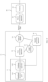
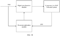
- the following describes a compensation manner of the nonlinear compensation apparatus when the electro-optical signal conversion apparatus is an EML or a DML. It should be understood that the nonlinear compensation apparatus in this embodiment includes a digital pre-distortion module and a parameter estimation module.
- the electro-optical signal conversion apparatus is an external modulator laser or a direct modulator laser.
- the digital pre-distortion module is configured to perform pre-distortion processing on the first baseband signal based on a distortion parameter.
- the parameter estimation module is configured to update the distortion parameter based on the first baseband signal and the second baseband signal to perform nonlinear compensation on the first baseband signal.
- the nonlinear compensation manner used in the first manner is a one-dimensional DPD nonlinear compensation manner.
- the one-dimensional DPD nonlinear compensation manner is performing nonlinear compensation by using a one-dimensional DPD model.
- the one-dimensional DPD model is not limited to a polynomial model and a neural network model.
- the electro-optical signal conversion apparatus is an external modulator laser.
- the digital pre-distortion module is configured to perform pre-distortion processing on the first baseband signal based on a distortion parameter.
- the parameter estimation module is configured to: obtain a difference between a preset bias voltage and a half-wave voltage of the external modulator laser based on the first baseband signal and the second baseband signal; and update the distortion parameter based on the difference to perform nonlinear compensation on the first baseband signal.
- the nonlinear compensation manner used in the first manner is a compensation manner based on the difference between the half-wave voltage of the external modulator laser EML and the preset bias voltage.
- N is greater than 1
- the structure of the communication device in the two possible implementations is applicable to compensation for nonlinear distortion of a single-wavelength and multi-frequency signal.
- the communication device further includes an electrical domain combiner and an electrical domain splitter.
- the electrical domain combiner is connected to the first processing apparatus.
- the electrical domain splitter is connected to the second processing apparatus.
- the first processing apparatus is specifically configured to convert the first baseband subsignals into the first radio frequency subsignals, and output the first radio frequency subsignals to the electrical domain combiner.
- the electrical domain combiner is configured to combine the N first radio frequency subsignals, and output a combined radio frequency signal to the first processing apparatus.
- the first processing apparatus is further specifically configured to convert the combined radio frequency signal into the optical signal.
- the second processing apparatus is specifically configured to convert the second optical signal into the second radio frequency signal, and output the second radio frequency signal to the electrical domain splitter.
- the electrical domain splitter is configured to split the second radio frequency signal into the N second radio frequency subsignals, and output the N second radio frequency subsignals to the second processing apparatus.
- the second processing apparatus is further specifically configured to convert the second radio frequency subsignals into the N second baseband subsignals.
- the first processing module includes an electro-optical signal conversion apparatus and N digital-to-analog conversion apparatuses.
- the second processing apparatus includes an optical-electro signal conversion apparatus and N analog-to-digital conversion apparatuses. There are N local oscillators. One local oscillator corresponds to one digital-to-analog conversion apparatus and one analog-to-digital conversion apparatus.
- the electrical domain combiner is separately connected to the N digital-to-analog conversion apparatuses and the electro-optical signal conversion apparatus.
- the N digital-to-analog conversion apparatuses are further connected to the nonlinear compensation apparatus.
- Each local oscillator is separately connected to a corresponding digital-to-analog conversion apparatus and a corresponding analog-to-digital conversion apparatus.
- the optical splitter is separately connected to the electro-optical signal conversion apparatus and the optical-electro signal conversion apparatus.
- the electrical domain splitter is separately connected to the optical-electro signal conversion apparatus and the N analog-to-digital conversion apparatuses.
- the N analog-to-digital conversion apparatuses are all connected to the nonlinear compensation apparatus.
- the first processing module further includes N first frequency mixers and N bandpass filters.
- One digital-to-analog conversion apparatus corresponds to one first frequency mixer, one bandpass filter, and one local oscillator.
- the second processing apparatus further includes N second frequency mixers and N low-pass filters.
- One analog-to-digital conversion apparatus corresponds to one second frequency mixer, one low-pass filter, and one local oscillator.
- the first processing apparatus further includes N variable attenuators and N low noise amplifiers.
- One bandpass filter corresponds to one variable attenuator and one low noise amplifier.
- the first processing apparatus further includes an optical domain amplifier.
- the second processing apparatus further includes an electrical domain amplifier.
- the communication device includes an electrical domain combiner and N electrical domain switches.
- the electrical domain splitter is connected to the second processing apparatus.
- the electrical domain switch is separately connected to the local oscillator and the second processing apparatus.
- One electrical domain switch corresponds to one first radio frequency subsignal.
- the second processing apparatus is specifically configured to convert the second optical signal into the second radio frequency signal.
- the electrical domain switch is configured to control connection and disconnection of a feedback link of a second radio frequency subsignal corresponding to a first radio frequency subsignal.
- the second processing apparatus is further specifically configured to convert a fed-back second radio frequency subsignal into a second baseband subsignal. In this manner, the electrical domain switch may be controlled to feed back a second baseband subsignal at a specific frequency and perform nonlinear compensation on the signal at such frequency.
- the first processing module includes an electro-optical signal conversion apparatus and N digital-to-analog conversion apparatuses.
- the second processing apparatus includes an optical-electro signal conversion apparatus and an analog-to-digital conversion apparatus.
- One local oscillator corresponds to one digital-to-analog conversion apparatus and one electrical domain switch.
- the electrical domain combiner is separately connected to the N digital-to-analog conversion apparatuses and the electro-optical signal conversion apparatus.
- the N digital-to-analog conversion apparatuses are further connected to the nonlinear compensation apparatus.
- Each local oscillator is connected to a corresponding digital-to-analog conversion apparatus and a corresponding electrical domain switch.
- the optical splitter is separately connected to the electro-optical signal conversion apparatus and the optical-electro signal conversion apparatus.
- the analog-to-digital conversion apparatus is separately connected to the optical-electro signal conversion apparatus, the N electrical domain switches, and the nonlinear compensation apparatus.
- the first processing module further includes N first frequency mixers and N bandpass filters.
- One digital-to-analog conversion apparatus corresponds to one first frequency mixer, one bandpass filter, and one local oscillator.
- the second processing apparatus further includes a second frequency mixer and a low-pass filter.
- the first processing apparatus further includes N variable attenuators and N low noise amplifiers.
- One bandpass filter corresponds to one variable attenuator and one low noise amplifier.
- the first processing apparatus further includes an optical domain amplifier.
- the second processing apparatus further includes an electrical domain amplifier. It should be understood that for a connection manner of the components in this manner, refer to the following Embodiment 5.
- the structure of the communication device in the foregoing two possible implementations is applicable to compensation for nonlinear distortion of the single-wavelength and multi-frequency signal.
- a structure of the communication device in the following two possible implementations is applicable to compensation for nonlinear distortion of a multi-wavelength and multi-frequency signal.
- the communication device further includes a wavelength division multiplexer and a wavelength division demultiplexer.
- the wavelength division multiplexer is separately connected to the first processing apparatus and the optical splitter.
- the wavelength division demultiplexer is separately connected to the optical splitter and the second processing apparatus.
- the first processing apparatus is specifically configured to convert the first baseband subsignals into the first radio frequency subsignals, and convert the first radio frequency subsignals into N first optical subsignals.
- the optical signal includes the N first optical subsignals.
- the wavelength division multiplexer is configured to combine the N first optical subsignals, and output a combined optical signal to the optical splitter.
- the wavelength division demultiplexer is configured to split the second optical signal into N second optical subsignals.
- the second processing apparatus is specifically configured to convert the second optical subsignals into the second radio frequency subsignals, and convert the second radio frequency subsignals into the N second baseband subsignals.
- the first processing module includes N digital-to-analog conversion apparatuses and N electro-optical signal conversion apparatuses.
- One digital-to-analog conversion apparatus corresponds to one electro-optical signal conversion apparatus.
- the second processing apparatus includes N optical-electro signal conversion apparatuses and N analog-to-digital conversion apparatuses.
- One optical-electro signal conversion apparatus corresponds to one analog-to-digital conversion apparatus.
- One local oscillator corresponds to one digital-to-analog conversion apparatus and one analog-to-digital conversion apparatus.
- the nonlinear compensation apparatus is connected to the N digital-to-analog conversion apparatuses.
- Each digital-to-analog conversion apparatus is connected to a corresponding electro-optical signal conversion apparatus and a corresponding local oscillator.
- the wavelength division multiplexer is separately connected to the N electro-optical signal conversion apparatuses and the optical splitter.
- the wavelength division demultiplexer is separately connected to the N optical-electro signal conversion apparatuses and the optical splitter.
- Each analog-to-digital conversion apparatus is further connected to a corresponding optical-electro signal conversion apparatus and a corresponding local oscillator.
- the N analog-to-digital conversion apparatuses are all connected to the nonlinear compensation apparatus.
- the first processing module further includes N first frequency mixers and N bandpass filters.
- the second processing apparatus further includes N second frequency mixers and N low-pass filters.
- the first processing apparatus further includes N variable attenuators and N low noise amplifiers.
- the first processing apparatus further includes an optical domain amplifier.
- the second processing apparatus further includes an electrical domain amplifier.
- the communication device further includes a wavelength division multiplexer and a wavelength division demultiplexer.
- the communication device in this manner further includes 2N electrical domain switches.
- the local oscillator is connected to N electrical domain switches.
- the N electrical domain switches are further connected to the second processing apparatus.
- One electrical domain switch corresponds to one first radio frequency subsignal.
- the second processing apparatus is further connected to remaining N electrical domain switches.
- One electrical domain switch corresponds to one second radio frequency subsignal.
- One first radio frequency subsignal corresponds to one second radio frequency subsignal.
- the electrical domain switch is configured to control connection and disconnection of a feedback link of a second radio frequency subsignal corresponding to a first radio frequency subsignal.
- the second processing apparatus is further specifically configured to convert a fed-back second radio frequency subsignal into a second baseband subsignal. In this manner, the electrical domain switch may be controlled to feed back a second baseband subsignal at a specific frequency and perform nonlinear compensation on the signal at such frequency.
- the first processing module includes N digital-to-analog conversion apparatuses and N electro-optical signal conversion apparatuses.
- One digital-to-analog conversion apparatus corresponds to one electro-optical signal conversion apparatus.
- the second processing apparatus includes N optical-electro signal conversion apparatuses and an analog-to-digital conversion apparatus.
- One optical-electro signal conversion apparatus corresponds to one electrical domain switch.
- One local oscillator corresponds to one digital-to-analog conversion apparatus, one electrical domain switch, and one analog-to-digital conversion apparatus.
- the nonlinear compensation apparatus is connected to the N digital-to-analog conversion apparatuses.
- Each digital-to-analog conversion apparatus is connected to a corresponding electro-optical signal conversion apparatus and a corresponding local oscillator. Each local oscillator is further connected to a corresponding electrical domain switch.
- the wavelength division multiplexer is separately connected to the N electro-optical signal conversion apparatuses and the optical splitter.
- the wavelength division demultiplexer is separately connected to the N optical-electro signal conversion apparatuses and the optical splitter.
- Each optical-electro signal conversion apparatus is connected to a corresponding electrical domain switch.
- the 2N electrical domain switches are all connected to the analog-to-digital conversion apparatus.
- the analog-to-digital conversion apparatus is further connected to the nonlinear compensation apparatus.
- the first processing module further includes N first frequency mixers and N bandpass filters.
- the second processing apparatus further includes a second frequency mixer and a low-pass filter.
- the first processing apparatus further includes N variable attenuators and N low noise amplifiers.
- the first processing apparatus further includes an optical domain amplifier.
- the second processing apparatus further includes an electrical domain amplifier.
- the nonlinear compensation apparatus in this embodiment includes a digital pre-distortion module and a parameter estimation module.
- the electro-optical signal conversion apparatus is an external modulator laser or a direct modulator laser.
- the digital pre-distortion module is configured to perform pre-distortion processing on the first baseband subsignals based on a distortion parameter.
- the parameter estimation module is configured to update the distortion parameter based on the first baseband subsignals and the second baseband subsignals to perform nonlinear compensation on the first baseband subsignals.
- the nonlinear compensation manner used in the first manner is a multi-dimensional DPD nonlinear compensation manner.
- a multi-dimensional DPD model is not limited to a polynomial model and a neural network model. The manner of performing compensation by using the multi-dimensional DPD model can compensate for nonlinear distortion of a single baseband signal in a transmission process, and can also compensate for nonlinear distortion caused by inter-modulation and crosstalk between a plurality of baseband signals.
- the electro-optical signal conversion apparatus is an external modulator laser.
- the digital pre-distortion module is configured to perform pre-distortion processing on the first baseband subsignals based on a distortion parameter.
- the parameter estimation module is configured to: obtain a difference between a preset bias voltage and a half-wave voltage of the external modulator laser based on the first baseband subsignals and the second baseband subsignals; and update the distortion parameter based on the difference to perform nonlinear compensation on the first baseband subsignals. It should be understood that, in this manner, for a manner of performing nonlinear compensation on the first baseband subsignals, refer to related descriptions of performing nonlinear compensation on the first baseband signal in the foregoing manner.
- an embodiment of this application provides a communication system, including the communication device according to the first aspect and a remote-side communication device.
- the communication device according to the first aspect is a central-side communication device in a remote communication system.
- the remote-side communication device is configured to convert a first optical signal from the central-side communication device into a radio frequency signal, and transmit the radio frequency signal through an antenna.
- Embodiments of this application provide a communication device and system.
- the communication device is a central-side communication device.
- a feedback link is established in the central-side communication device.
- the feedback link is used to feed back a baseband signal that has nonlinear distortion and that is processed by a component in the central-side communication device.
- the central-side communication device may compensate for nonlinear distortion of the baseband signal based on a generated baseband signal and the signal fed back through the feedback link. This improves signal transmission quality.
- Nonlinear distortion in a RoF network system mainly occurs in the central-side communication device.
- nonlinear distortion in the RoF network system can be compensated for, an additional optical fiber does not need to be disposed, and complex control logic can be avoided when the feedback link needs to be established between the central-side communication device and a remote-side communication device. This simplifies a disposing manner on a remote side.
- a remote network system includes a central-side communication device and at least one remote-side communication device.
- the central-side communication device generates a baseband signal
- the remote-side communication device transmits a radio frequency signal converted from the baseband signal, for access and use by a user terminal.
- FIG. 1 is a schematic diagram of a structure of a remote network system for transmitting a signal through a coaxial cable in a conventional technology.
- a central-side communication device 10 and a remote-side communication device are connected through the coaxial cable.
- the central-side communication device 10 includes a baseband signal processing unit (digital unit, DU) and a radio frequency signal processing unit (radio unit, RU).
- the remote-side communication device 20 includes a radio frequency signal transmitting unit.
- the radio frequency signal transmitting unit is, for example, a radio head (radio head, RH).
- the central-side communication device 10 generates a baseband signal, converts the baseband signal into a radio frequency signal through the DU and the RU, and further transmits the radio frequency signal to the remote-side communication device 20 through the coaxial cable.
- the remote-side communication device 20 may transmit the received radio frequency signal through the RH.
- a radio frequency signal is transmitted through a coaxial cable, resulting in a low transmission rate.
- FIG. 2 is a schematic diagram of a structure of a CPRI network system in the conventional technology.
- a central-side communication device 10 and a remote-side communication device 20 are connected through an optical fiber.
- the central-side communication device 10 includes a DU
- the remote-side communication device 20 includes an RU and an RH.
- the central-side communication device 10 transmits the baseband signal to the remote-side communication device 20 through the optical fiber.
- the remote-side communication device 20 may convert the baseband signal into a radio frequency signal through the RU, and transmit the radio frequency signal through the RH.
- the optical fiber for transmitting the baseband signal in the CPRI network system and the eCPRI network system has a transmission rate higher than that of the coaxial cable for signal transmission, the signal transmission rate is still lower than that of a radio over fiber network system in FIG. 3 .
- FIG. 3 is a schematic diagram of a structure of a radio over fiber network system in the conventional technology.
- a central-side communication device 10 includes a DU, an RU, and an electro-optical signal conversion apparatus
- a remote-side communication device 20 includes an optical-electro signal conversion apparatus and an RH.
- the central-side communication device converts a generated baseband signal into a radio frequency signal, converts the radio frequency signal into an optical signal by using the electro-optical signal conversion apparatus, and then transmits the optical signal to the remote-side communication device through an optical fiber.
- the remote-side communication device converts the received optical signal into a radio frequency signal by using the optical-electro signal conversion apparatus, and further transmits the radio frequency signal through the RH.
- the RoF network system simplifies a manner of disposing the remote-side communication device.
- a plurality of components such as the DU, the RU, and the electro-optical signal conversion apparatus are disposed in the central-side communication device, so that costs of the remote-side communication device can be effectively reduced, and it is convenient to quickly deploy the remote-side communication device, to improve network coverage.
- the radio frequency signal needs to be converted into the optical signal by using the electro-optical signal conversion apparatus.
- the electro-optical signal conversion apparatus is prone to generating nonlinear distortion in a signal conversion process, and dispersion also causes nonlinear distortion of the optical signal in a transmission process of the optical signal. Consequently, the optical signal transmitted in the RoF network system has nonlinear distortion. This results in low quality of the optical signal.
- FIG. 4 is a first schematic diagram of a structure of an electro-optical signal conversion apparatus in a RoF network system provided in the conventional technology.
- the electro-optical signal conversion apparatus in a structure of the RoF network system is an external modulator laser (external modulator laser, EML).
- the EML may include a bias voltage adjustment unit and a dispersion compensation unit.
- Nonlinear distortion generated by the electro-optical signal conversion apparatus in the signal conversion process may cause a change in a bias voltage of the electro-optical signal conversion apparatus. Therefore, in FIG. 4 , the bias voltage adjustment unit may be used to adjust the bias voltage of the electro-optical signal conversion apparatus, to eliminate nonlinear distortion generated by the electro-optical signal conversion apparatus in the signal conversion process.
- the dispersion compensation unit may further perform nonlinear compensation on nonlinear distortion caused by dispersion of the optical signal, to eliminate nonlinear distortion caused by transmission of the optical signal.
- the compensation method in FIG. 4 only considers nonlinear compensation performed when the electro-optical signal conversion apparatus is an EML.
- the compensation method is not applicable to a scenario in which the electro-optical signal conversion apparatus is a direct modulator laser (direct modulator laser, DML), and applicability is limited.
- compensation effect of the dispersion compensation unit in this compensation manner on nonlinear distortion is related to a wavelength of an optical signal and a length of an optical fiber, and robustness of the compensation effect is poor and costs are high.
- this compensation manner does not consider linear distortion caused by a memory characteristic of the EML.
- the memory characteristic is a characteristic that a signal transmitted at a previous moment in a signal transmission process affects a subsequently transmitted signal, and this characteristic is an inherent characteristic related to a component.
- Nonlinear distortion may include lower-order nonlinear distortion and higher-order nonlinear distortion. Higher-order nonlinear distortion has greater impact on quality of an optical signal. Therefore, based on FIG. 4 , to further improve compensation effect on negative nonlinear distortion, FIG. 5 provides a higher-order nonlinear distortion compensation method.
- FIG. 5 is a second schematic diagram of a structure of an electro-optical signal conversion apparatus in a RoF network system provided in the conventional technology. As shown in FIG. 5 , the electro-optical signal conversion apparatus in the RoF network system structure is an external modulator laser EML.
- the EML may include a higher-order nonlinear distortion compensation unit.
- the higher-order nonlinear distortion compensation unit includes a bias voltage adjustment unit and a dispersion compensation unit. Different from FIG.
- the dispersion compensation unit compensates for second-order nonlinear distortion
- the bias voltage adjustment unit compensates for third-order or higher-order nonlinear distortion. Therefore, compensation effect of the nonlinear compensation method in FIG. 5 is more obvious. However, the method in FIG. 5 still has the same problem as that in FIG. 4 .
- FIG. 6 provides a memory polynomial-based digital pre-distortion (digital pre-distortion, DPD) nonlinear compensation method.
- FIG. 6 is a third schematic diagram of a structure of an electro-optical signal conversion apparatus in a RoF network system provided in the conventional technology. As shown in FIG. 6 , the electro-optical signal conversion apparatus in a structure of the RoF network system may be an EML or a DML. The electro-optical signal conversion apparatus includes a DPD compensation unit.
- the DPD compensation unit performs, based on a signal input to the electro-optical signal conversion apparatus and a signal output by the electro-optical signal conversion apparatus, nonlinear compensation on nonlinear distortion generated by the electro-optical signal conversion apparatus in a signal conversion process.
- the DPD nonlinear compensation method may be applicable to the EML or the DML and further considers nonlinear distortion caused by a memory characteristic of the electro-optical signal conversion apparatus, nonlinear compensation effect can be improved.
- the nonlinear compensation method in FIG. 6 is applicable only to the electro-optical signal conversion apparatus and does not consider nonlinear distortion caused by another component, for example, a power amplifier (power amplifier, PA), generally included in the RoF network system. Therefore, the RoF network system further has nonlinear distortion.
- PA power amplifier
- FIG. 7 provides a memory polynomial-based digital pre-distortion (digital pre-distortion, DPD) nonlinear compensation method.
- FIG. 7 is a schematic diagram of a structure of a RoF network system provided in the conventional technology.
- the RoF network system also includes a central-side communication device 10 and a remote-side communication device 20.
- a central-side communication device 10 and a remote-side communication device 20 For a specific manner of disposing components in the central-side communication device 10 and the remote-side communication device 20, refer to FIG. 3 .
- the remote-side communication device 20 in FIG. 7 further includes a radio frequency signal division apparatus, and the RoF network system further includes a feedback link.
- the radio frequency signal division apparatus transmits a part of radio frequency signals that are from an optical-electro signal conversion apparatus, and outputs the other part of radio frequency signals to the feedback link.
- the remote-side communication device 20 includes an electro-optical signal conversion apparatus. The other part of radio frequency signals are converted into an optical signal by using the optical-electro signal conversion apparatus and then fed back to the central-side communication device.
- the central-side communication device 10 After converting the fed-back optical signal into a baseband signal, the central-side communication device 10 compares the baseband signal with a baseband signal output by the central-side communication device and performs analysis to determine nonlinear distortion of the baseband signal, and further adjusts a parameter of the baseband signal to compensate for nonlinear distortion in a signal conversion process.
- the method shown in FIG. 7 can compensate for nonlinear distortion caused by other components disposed in the RoF network system, because the remote-side communication device needs to feed back the optical signal in the method shown in FIG. 7 , an additional optical fiber needs to be disposed between the central-side communication device and the remote-side communication device to establish the feedback link.
- the optical signal and the uplink data may share a same link (for example, the optical fiber connecting the electro-optical signal conversion apparatus and the optical-electro signal conversion apparatus in FIG. 7 ).
- additional control logic needs to be configured on the central-side communication device and the remote-side communication device, to implement switching between the uplink data and the fed-back optical signal by the central-side communication device. This results in high complexity.
- the existing RoF network system simplifies a manner of disposing the remote-side communication device.
- a plurality of components such as a DU, an RU, and the electro-optical signal conversion apparatus are integrated into the central-side communication device. Therefore, nonlinear distortion in the RoF network system mainly occurs in the central-side communication device. Therefore, to resolve the foregoing technical problem, the feedback link is established in the central-side communication device in this embodiment of this application, so that nonlinear distortion in the RoF network system can be compensated for, the additional optical fiber does not need to be disposed, and complex control logic can be avoided when the feedback link needs to be established between the central-side communication device and the remote-side communication device. This simplifies a disposing manner on a remote side.
- FIG. 8 is a schematic diagram of an architecture of a RoF network system according to an embodiment of this application.
- the RoF network system includes a central-side communication device 10 and a plurality of remote-side communication devices 20.
- the central-side communication device 10 and the plurality of remote-side communication devices 20 are connected through an optical fiber.
- the in-between optical fiber may be 5 km to 50 km.
- the central-side communication device in FIG. 8 includes at least one analog baseband unit (baseband unit, BBU), and each remote-side communication device includes a remote radio unit (remote radio unit, RRU).
- BBU baseband unit
- RRU remote radio unit
- the RoF network system in this embodiment of this application is applicable to scenarios such as a macro cell (macro cell) and a small cell, for example, a millimeter-wave small cell (Millimeter-wave small cell, mmWave small cell) and a hot-spot area (hot-spot area).
- the remote-side communication device may be a base station.
- the base station may be a base transceiver station (Base Transceiver Station, BTS for short) in a GSM system or a CDMA system, or may be a base station (NodeB, NB for short) in a WCDMA system, or may be an evolved NodeB (evolved NodeB, eNB for short) or a next-generation base station (which may be collectively referred to as a next-generation radio access network node (NG-RAN node) in an LTE system.
- the next-generation base station includes a new radio base station (NR nodeB, gNB) and a next-generation evolved base station (NG-eNB). This is not limited herein.
- FIG. 9 is a schematic diagram of a structure of a RoF network system according to an embodiment of this application.
- the RoF network system in this embodiment of this application includes a central-side communication device 10 and at least one remote-side communication device. It should be understood that FIG. 9 describes an example of one remote-side communication device.
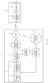
- the central-side communication device 10 includes a digital processing apparatus 11, a first processing apparatus 12, an optical splitter 13, a second processing apparatus 14, and a local oscillator 15.
- the first processing apparatus 12 is separately connected to the digital processing apparatus 11, the local oscillator 15, and the optical splitter 13.
- the optical splitter 13 is further connected to the second processing apparatus 14.
- the second processing apparatus 14 is further connected to the local oscillator 15 and the digital processing apparatus 11.
- the digital processing apparatus 11 is configured to generate a first baseband signal, and output the first baseband signal to the first processing apparatus 12.
- the digital processing apparatus 11 in this embodiment of this application may generate a baseband signal source, for example, a baseband resource pool.
- the first processing apparatus 12 is configured to convert the first baseband signal into a first radio frequency signal, convert the first radio frequency signal into an optical signal, and output the optical signal to the optical splitter 13.
- the local oscillator 15 in this embodiment of this application is configured to generate a radio frequency signal.
- the first baseband signal in this embodiment of this application may be a digital baseband signal.
- the first processing apparatus 12 may convert the first baseband signal into the first radio frequency signal through the local oscillator 15, and convert the first radio frequency signal into the optical signal.
- the first processing apparatus 12 may convert the first baseband signal into the first radio frequency signal at a specific frequency through the local oscillator 15.
- the optical splitter 13 After the optical splitter 13 receives the optical signal from the first processing apparatus 12, the optical splitter 13 is configured to split the optical signal into a first optical signal and a second optical signal, output the first optical signal to at least one remote-side communication device, and output the second optical signal to the second processing apparatus 14.
- the first optical signal and the second optical signal in this embodiment of this application have a same wavelength but different powers.
- the optical signal is split into the first optical signal and the second optical signal at a power ratio of 9:1, where a power percentage of the first optical signal is 90%, and a power percentage of the second optical signal is 10%.
- the central-side communication device 10 transmits the analog baseband signal to the remote-side communication device 20 through an optical fiber, where the analog baseband signal is transmitted through the optical fiber.
- the central-side communication device 10 in this embodiment of this application may convert a digital baseband signal into a radio frequency signal, convert the radio frequency signal into an optical signal, and transmit the optical signal to the remote-side communication device 20 through an optical fiber.
- the central-side communication device 10 may transmit a radio frequency signal.
- the central-side communication device 10 transmits the baseband signal.
- the baseband signal is a signal whose center frequency is 0 Hz, but the radio frequency signal may correspond to different frequencies. Therefore, the network system in this embodiment of this application may transmit a multi-frequency signal.
- the CPRI/eCPRI network system may only transmit a single-frequency signal.
- the communication standard may be a communication standard such as a long term evolution (long term evolution, LTE) communication standard, a universal mobile telecommunications system (universal mobile telecommunications system, UMTS) communication standard, a wireless-fidelity (wireless-fidelity, Wi-Fi) communication standard, or a millimeter-wave communication standard. Therefore, the network system in this embodiment of this application may be applied to the scenario of the plurality of communication standards. However, the CPRI/eCPRI network system may be only applicable to a scenario of one communication standard.
- the remote-side communication device 20 may include a third processing apparatus 21 and an antenna 22.
- the third processing apparatus 21 may convert the first optical signal into a radio frequency signal, and output the radio frequency signal to the antenna 22.
- the antenna 22 transmits the radio frequency signal, for access and use by a user.
- the second processing apparatus 14 is configured to convert the second optical signal into a second radio frequency signal, convert the second radio frequency signal into a second baseband signal, and output the second baseband signal to the digital processing apparatus 11.
- the second baseband signal is a digital baseband signal.
- the second processing apparatus 14 may convert an optical signal into an electrical domain signal, convert the electrical domain signal into a second radio frequency signal through the local oscillator 15, and convert the second radio frequency signal into a second baseband signal. It should be understood that, in this embodiment of this application, the second radio frequency signal and the first radio frequency signal have a same frequency.
- the digital processing apparatus 11 is further configured to perform nonlinear compensation on the first baseband signal based on the first baseband signal and the second baseband signal.
- the digital processing apparatus 11 may output the first baseband signal, and may further receive the second baseband signal processed by each component. Therefore, nonlinear compensation may be performed on the first baseband signal by comparing the first baseband signal with the second baseband signal and performing analysis, to eliminate nonlinear distortion of the first baseband signal. This improves quality of the first baseband signal, and correspondingly improves quality of a signal transmitted in the RoF network system.
- the digital processing apparatus 11 in this embodiment may include a baseband resource pool 111 and a nonlinear compensation apparatus 112.
- the baseband resource pool 111 is connected to the nonlinear compensation apparatus 112.
- the nonlinear compensation apparatus 112 is further separately connected to the first processing apparatus 12 and the second processing apparatus 14.
- an arrow in FIG. 9 may represent a signal transmission direction, or may represent a connection in the central-side communication device 10. Explanations of arrows in the following figures are the same as those in FIG. 9 .
- the first baseband signal includes N first baseband subsignals
- the second baseband signal includes N second baseband subsignals
- the first radio frequency signal includes N first radio frequency subsignals
- the second radio frequency signal includes N second radio frequency subsignals
- the first radio frequency subsignals one-to-one correspond to the second radio frequency subsignals based on frequencies
- N is an integer greater than or equal to 1.
- the baseband resource pool 111 is configured to generate the N first baseband subsignals, and output the N first baseband subsignals to the first processing apparatus 12 by using the nonlinear compensation apparatus 112.
- the first processing apparatus is specifically configured to convert the first baseband subsignals into the first radio frequency subsignals, convert the N first radio frequency subsignals into the optical signal.
- the second processing apparatus is specifically configured to convert the second optical signal into the N second radio frequency subsignals, convert the second radio frequency subsignals into the second baseband subsignals.
- the N second radio frequency subsignals are generated after the N first baseband subsignals are processed by the first processing apparatus 12, the optical splitter 13, and the second processing apparatus 14.
- the first radio frequency subsignals one-to-one correspond to the second radio frequency subsignals based on frequencies. It should be understood that the first baseband subsignals converted into the first radio frequency subsignals also one-to-one correspond to the second baseband subsignals converted from the second radio frequency subsignals at a same frequency as the first radio frequency subsignals.
- the nonlinear compensation apparatus 112 is configured to perform nonlinear compensation on the first baseband subsignals based on the first baseband subsignals and the second baseband subsignals corresponding to the first baseband subsignals. It should be understood that, for steps performed by the baseband resource pool 111 herein, refer to the foregoing step of generating the first baseband signal in the digital processing apparatus 11, and for steps performed by the nonlinear compensation apparatus 112, refer to the foregoing step of performing nonlinear compensation in the digital processing apparatus 11.
- the baseband resource pool 111 may include N baseband resources. Each baseband resource is used to generate one first baseband subsignal. It should be noted that, in this embodiment of this application, a wavelength of the optical signal may be 1310 nm.
- a dispersion characteristic of the optical signal causes nonlinear distortion, and this phenomenon is particularly serious in a transmission process of an optical signal with a 1550 nm wavelength.
- a dispersion phenomenon is not obvious in a transmission process of the optical signal with a 1310 nm wavelength.
- the optical signal with a 1550 nm wavelength is frequently used. Therefore, nonlinear distortion caused by dispersion needs to be compensated for during transmission of the optical signal on such frequency band.
- nonlinear distortion caused by dispersion of the optical signal in the RoF network system is low and may be ignored.
- nonlinearity of a component in the central-side communication device may be locally compensated for to improve overall performance of the RoF network system.
- the technical solution in this embodiment of this application may also be applied to an optical fiber communication system for a 1550 nm wavelength and another different wavelength.
- optical signal is transmitted through the optical fiber.
- a feedback link is established in the central-side communication device.
- the feedback link is used to feed back a baseband signal that has nonlinear distortion and that is processed by a component in the central-side communication device.
- the central-side communication device may compensate for nonlinear distortion of the baseband signal based on a generated baseband signal and the signal fed back through the feedback link. This improves signal transmission quality.
- Nonlinear distortion in the RoF network system mainly occurs in the central-side communication device.
- nonlinear distortion in the RoF network system can be compensated for, an additional optical fiber does not need to be disposed, and complex control logic can be avoided when the feedback link needs to be established between the central-side communication device and the remote-side communication device. This simplifies a disposing manner on a remote side.
- the baseband resource pool 111 may generate N first baseband subsignals at different frequencies.
- the following embodiments separately describes a structure of the RoF network system provided in this embodiment of this application when N is 1 and when N is greater than 1.
- the following Embodiment 2 and Embodiment 3 describe a structure of the RoF network system when N is 1
- Embodiment 4 to Embodiment 7 describe a structure of the RoF network system when N is greater than 1.
- a first baseband signal in the following Embodiment 2 to Embodiment 7 is a digital baseband signal.
- FIG. 10 is a schematic diagram of a structure of a RoF network system according to another embodiment of this application.
- a first processing apparatus 12 in a central-side communication device 10 in this embodiment of this application may include a DAC digital-to-analog conversion apparatus 121, a first frequency mixer 122, a bandpass filter 123, and an electro-optical (electro-optical, E/O) conversion apparatus 124.
- a second processing apparatus 14 may include an optical-electro (optical-electro, O/E) conversion apparatus 141, a second frequency mixer 142, a low-pass filter 143, and an ADC analog-to-digital conversion apparatus 144.
- the structure of the RoF network system provided in Embodiment 2 is applicable to a single-wavelength and single-frequency baseband signal.
- the electro-optical signal conversion apparatus 124 in this embodiment of this application may be an EML or a DML.
- the optical-electro (optical-electro, O/E) conversion apparatus may also be referred to as a photo detector (photo detector, PD).
- the digital-to-analog conversion apparatus 121 is separately connected to the nonlinear compensation apparatus 112 and the first frequency mixer 122.
- the bandpass filter 123 is separately connected to the first frequency mixer 122 and the electro-optical signal conversion apparatus 124.
- the first frequency mixer 122 is further connected to the local oscillator 15.
- the electro-optical signal conversion apparatus 124 is further connected to the optical splitter 13.
- the second frequency mixer 142 is separately connected to the optical-electro signal conversion apparatus 141, the low-pass filter 143, and the local oscillator 15.
- the analog-to-digital conversion apparatus 144 is separately connected to the low-pass filter 143 and the nonlinear compensation apparatus 112.
- the digital-to-analog conversion apparatus 121 is configured to convert a first baseband signal into a first digital baseband signal, and output the first digital baseband signal to the first frequency mixer 122.
- the first frequency mixer 122 is configured to perform an up-conversion operation on the first digital baseband signal, convert the first digital baseband signal into a first radio frequency signal at a corresponding frequency through the local oscillator 15, and output the first radio frequency signal to the bandpass filter 123.
- the bandpass filter 123 is configured to filter the first radio frequency signal to filter out an interference signal in the first radio frequency signal, and output the filtered first radio frequency signal to the electro-optical signal conversion apparatus 124.
- the electro-optical signal conversion apparatus 124 is configured to convert the received first radio frequency signal into an optical signal, and output the optical signal to the optical splitter 13.
- the optical-electro signal conversion apparatus 141 is configured to convert a second optical signal into a second electrical domain signal, and output the second electrical domain signal to the second frequency mixer 142.
- the second frequency mixer 142 is configured to perform a down-conversion operation on the second electrical domain signal, convert the second electrical domain signal into a second radio frequency signal at a same frequency as the first radio frequency signal through the local oscillator 15, and output the second radio frequency signal to the low-pass filter 143.
- the low-pass filter 143 is configured to filter the second radio frequency signal to filter out an interference signal in the second radio frequency signal, and output the filtered second radio frequency signal to the analog-to-digital conversion apparatus 144.
- the analog-to-digital conversion apparatus 144 is configured to convert the second radio frequency signal into a second baseband signal, and output the second baseband signal to the nonlinear compensation apparatus 112.
- the first processing apparatus 12 may further include a variable attenuator 125 and a low noise amplifier 126.
- the variable attenuator 125 is separately connected to the bandpass filter 123 and the low noise amplifier 126.
- the low noise amplifier 126 is further connected to the electro-optical signal conversion apparatus 124.
- the variable attenuator 125 is configured to adjust a power of the first radio frequency signal.
- the low noise amplifier 126 is configured to reduce noise in the first radio frequency signal.
- the first processing apparatus 12 may further include an optical domain amplifier 127 (erbium-doped fiber amplifier, EDFA).
- the optical domain amplifier 127 is separately connected to the electro-optical signal conversion apparatus 124 and the optical splitter 13.
- the optical domain amplifier 127 is configured to amplify a power of the optical signal.
- the second processing apparatus 14 may further include an electrical domain amplifier 145.
- the electrical domain amplifier 145 is separately connected to the low-pass filter 143 and the analog-to-digital conversion apparatus 144.
- the electrical domain amplifier 145 is configured to amplify a power of the second radio frequency signal.
- the second processing apparatus 14 may further include an electrical domain amplifier 145.
- the electrical domain amplifier 145 is separately connected to the digital-to-analog conversion apparatus 121 and the low-pass filter 143.
- a third processing apparatus 21 in the remote-side communication device 20 may include an optical-electro signal conversion apparatus 141.
- the optical-electro signal conversion apparatus 141 is connected to the optical splitter 13 through an optical fiber.
- the optical-electro signal conversion apparatus 141 is configured to convert a first optical signal into a radio frequency signal and output the radio frequency signal to an antenna 22.
- the antenna 22 may output the radio frequency signal.
- the nonlinear compensation apparatus 112 may include a digital pre-distortion module 1121 and a parameter estimation module 1122.
- the digital pre-distortion module 1121 is separately connected to the baseband resource pool 111, the first processing apparatus 12, and the second processing apparatus 14.
- the digital pre-distortion module 1121 is connected to the digital-to-analog conversion apparatus 121 in the first processing apparatus 12.
- the parameter estimation module 1122 is separately connected to the digital pre-distortion module 1121, and the analog-to-digital conversion apparatus 144 in the second processing apparatus 14.
- the digital pre-distortion module 1121 is configured to perform pre-distortion processing on the first baseband signal based on a distortion parameter.
- the distortion parameter may be predefined.
- the parameter estimation module 1122 is configured to update the distortion parameter based on the first baseband signal and the second baseband signal to perform nonlinear compensation on the first baseband signal. It should be understood that the method used in this embodiment of this application is a DPD nonlinear compensation method based on a model.
- the model is not limited to a polynomial model or a neural network model.
- nonlinear distortion in the system may be represented by using a polynomial model, for example, a Volterra polynomial, a memory polynomial (memory polynomial, MP), a generalized memory polynomial (generalized memory polynomial, GMP), and a Wiener-Hammerstein (W-H) polynomial.
- a polynomial model for example, a Volterra polynomial, a memory polynomial (memory polynomial, MP), a generalized memory polynomial (generalized memory polynomial, GMP), and a Wiener-Hammerstein (W-H) polynomial.
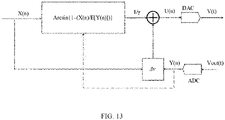
- FIG. 11 is a schematic diagram of one-dimensional DPD nonlinear compensation according to an embodiment of this application.
- an input signal for example, the first baseband signal
- an output signal for example, the first baseband signal
- y(n) for example, the first baseband signal
- a km indicates a parameter of a nonlinear term when nonlinear distortion in the RoF network system has an order k and a memory depth m
- k is the order of nonlinear distortion in the RoF network system
- m is the memory depth of nonlinear distortion in the RoF network system.
- W km indicates an updated distortion parameter
- the updated distortion parameter is obtained by solving W km , and pre-distortion processing is performed on the first baseband signal based on the updated distortion parameter, so that a linear optical signal is obtained after the first baseband signal is processed by the first processing apparatus 12, to improve quality of the optical signal.
- an algorithm for obtaining the updated distortion parameter in this embodiment of this application is not limited to a least square method, a least mean square method, a singular value decomposition method, or the like.
- the updated distortion parameter may be obtained in a direct learning manner or an indirect learning manner.
- direct learning and indirect learning are two common training methods in a digital pre-distortion technology.
- the direct learning method a sent signal is directly compared with a fed-back signal, and then the distortion parameter is updated.
- the indirect learning method post-compensation is performed on a fed-back signal, the fed-back signal is compared with a sent signal, and the distortion parameter is updated based on a difference between the fed-back signal and the sent signal.
- the structure of the remote-side communication device 20 is the same as the structure in the foregoing Embodiment 1. Details are not described herein again.
- nonlinear compensation can be performed on a single-wavelength and single-frequency baseband signal.
- the DPD nonlinear compensation method can compensate for nonlinear distortion caused by a memory characteristic of a component, and is applicable to a plurality of types of electro-optical signal conversion apparatuses.
- this embodiment of this application may further include another component into which nonlinear compensation is introduced, for example, an optical domain amplifier.
- the nonlinear compensation method in this embodiment of this application may further compensate for nonlinear distortion caused by the another component into which nonlinear compensation is introduced.
- FIG. 12 is a schematic diagram of a structure of a RoF network system according to another embodiment of this application.
- FIG. 12 for structures and connection relationships of a first processing apparatus 12 and a second processing apparatus 14 in a central-side communication device 10 in this embodiment of this application, refer to related descriptions in the foregoing Embodiment 2.
- a digital pre-distortion module 1121 is configured to perform pre-distortion processing on a first baseband signal based on a distortion parameter.
- an electro-optical signal conversion apparatus 124 in this embodiment of this application is an EML.
- a parameter estimation module 1122 is configured to obtain a difference between a preset bias voltage and a half-wave voltage of the external modulator laser based on the first baseband signal and a second baseband signal, and further update the distortion parameter based on the difference to perform nonlinear compensation on the first baseband signal.
- the following describes a method for performing nonlinear compensation on the first baseband signal by adjusting the difference between the preset bias voltage and the half-wave voltage of the external modulator laser in this embodiment of this application.
- ⁇ ⁇ indicates the half-wave voltage of the EML
- ⁇ DC indicates the preset bias voltage
- ⁇ v indicates the difference between the half-wave voltage of the EML and the preset bias voltage
- P out indicates a power of an optical signal output by the EML
- ⁇ ( t ) indicates a voltage of a radio frequency signal input to the EML.
- FIG. 13 is a schematic diagram of nonlinear compensation of an EML according to an embodiment of this application. As shown in FIG. 13 , it is assumed that when an amplitude of a first radio frequency signal input to the EML is v(t), a second radio frequency signal output by an O/E end is v out ( t ) .
- ⁇ out t RGE in 2 ⁇ 1 ⁇ sin ⁇ ⁇ t + ⁇ ⁇ ⁇
- R indicates an equivalent resistance of the O/E end
- G indicates a link loss between the EML and the O/E end
- E in indicates a power of a signal input to the EML
- ⁇ indicates a loss of the O/E end.
- E [] indicates expectation calculation (averaging).
- the parameter estimation module 1122 in this embodiment of this application stores a table of correspondences between ⁇ v and U ( n ). After obtaining the difference between the half-wave voltage of the EML and the preset bias voltage, the parameter estimation module 1122 may obtain the updated distortion parameter by looking up the table, and further update the distortion parameter.
- the structure of the remote-side communication device 20 is the same as the structure in the foregoing Embodiment 1. Details are not described herein again.
- a nonlinear compensation apparatus may further adjust the difference between the preset bias voltage and the half-wave voltage of the external modulator laser based on the first baseband signal and the second baseband signal to compensate for nonlinear distortion in the RoF network system.
- a structure of the RoF network system provided in Embodiment 4 and Embodiment 5 is applicable to a single-wavelength and multi-frequency baseband signal. Because N is greater than 1, namely, because a baseband resource pool 111 may generate N first baseband subsignals, a first processing apparatus 12 and a second processing apparatus 14 in this embodiment of this application are different from those in Embodiment 2 and Embodiment 3. Because Embodiment 4 and Embodiment 5 include a plurality of first baseband subsignals, electrical domain signals corresponding to the plurality of first baseband subsignals may be combined in Embodiment 4 and Embodiment 5. For a specific structure of the RoF network system, refer to the following Embodiment 4 and Embodiment 5. Same components are not identified in the accompanying drawings in the following embodiments. For details, refer to the identifiers in FIG. 10 .
- a carrier modulation technology a wavelength division multiplexing (WDM) technology, a polarization multiplexing technology, and the like
- WDM wavelength division multiplexing
- a polarization multiplexing technology and the like
- coexistence and co-transmission of signals a baseband digital signal, an LTE signal, a UMTS signal, a Wi-Fi signal, a millimeter-wave signal, and the like
- performance of the central-side communication device 10 such as compatibility, a quantity of access users, and a throughput can be further improved.
- nonlinear distortion such as four-wave mixing and adjacent-wave crosstalk generated in a transmission process of the optical signal is also introduced. Therefore, in a structure of the RoF network system provided in the following four embodiments, nonlinear compensation may also be performed on nonlinear distortion such as four-wave mixing and adjacent-wave crosstalk.
- nonlinear compensation may also be performed on nonlinear distortion such as four-wave mixing and adjacent-wave crosstalk.
- FIG. 14 is a schematic diagram of a structure of a RoF network system according to another embodiment of this application.
- a central-side communication device 10 in this embodiment of this application may further include an electrical domain combiner 16 and an electrical domain splitter 17.
- the electrical domain combiner 16 is connected to a first processing apparatus 12.
- the electrical domain splitter 17 is connected to a second processing apparatus 14.
- the first processing apparatus 12 in this embodiment of this application is specifically configured to convert first baseband subsignals into first radio frequency subsignals, and output the first radio frequency subsignals to the electrical domain combiner 16.
- the electrical domain combiner 16 is configured to combine the N first radio frequency subsignals, and output a combined radio frequency signal to the first processing apparatus 12.
- the electrical domain combiner 16 combines the N first radio frequency subsignals into one radio frequency signal.
- the first processing apparatus 12 is further specifically configured to convert the combined radio frequency signal into an optical signal.
- the second processing apparatus 14 in this embodiment of this application is specifically configured to convert a second optical signal into a second radio frequency signal, and output the second radio frequency signal to the electrical domain splitter 17.
- the electrical domain splitter 17 is configured to split the second radio frequency signal into N second radio frequency subsignals, and output the N second radio frequency subsignals to the second processing apparatus 14.
- the N second radio frequency subsignals one-to-one correspond to the N first radio frequency subsignals based on frequencies.
- the second processing apparatus 14 is further specifically configured to convert the second radio frequency subsignals into N second baseband subsignals.
- FIG. 15 is a schematic diagram of a structure of a RoF network system according to another embodiment of this application.
- the first processing module includes an electro-optical signal conversion apparatus 124 and N digital-to-analog conversion apparatuses 121.
- the second processing apparatus 14 includes an optical-electro signal conversion apparatus 141 and N analog-to-digital conversion apparatuses 144.
- One local oscillator 15 corresponds to one digital-to-analog conversion apparatus 121 and one analog-to-digital conversion apparatus 144.
- the electrical domain combiner 16 is separately connected to the N digital-to-analog conversion apparatuses 121 and the electro-optical signal conversion apparatus 124.
- the N digital-to-analog conversion apparatuses 121 are further connected to the nonlinear compensation apparatus 112.
- Each local oscillator 15 is separately connected to a corresponding digital-to-analog conversion apparatus 121 and a corresponding analog-to-digital conversion apparatus 144.
- the optical splitter 13 is separately connected to the electro-optical signal conversion apparatus 124 and the optical-electro signal conversion apparatus 141.
- the electrical domain splitter 17 is separately connected to the optical-electro signal conversion apparatus 141 and the N analog-to-digital conversion apparatuses 144.
- the N analog-to-digital conversion apparatuses 144 are all connected to the nonlinear compensation apparatus 112.
- the digital-to-analog conversion apparatus 121 in this embodiment of this application is configured to convert the first baseband subsignals into the first radio frequency subsignals, and output the first radio frequency subsignals to the electrical domain combiner 16.
- the electro-optical signal conversion apparatus 124 is configured to convert the combined radio frequency signal into the optical signal.
- the optical-electro signal conversion apparatus 141 is configured to convert the second optical signal into the second radio frequency signal, and output the second radio frequency signal to the electrical domain splitter 17.
- the analog-to-digital conversion apparatus 144 is configured to convert the second radio frequency subsignals into the second baseband subsignals.
- the first processing apparatus 12 may further include N first frequency mixers 122 and N bandpass filters 123.
- One digital-to-analog conversion apparatus 121 corresponds to one first frequency mixer 122, one bandpass filter 123, and one local oscillator 15.
- the second processing apparatus 14 further includes N second frequency mixers 142 and N low-pass filters 143.
- One analog-to-digital conversion apparatus 144 corresponds to one second frequency mixer 142, one low-pass filter 143, and one local oscillator 15.
- Each first frequency mixer 122 is connected to a corresponding digital-to-analog conversion apparatus 121, a corresponding bandpass filter 123, and a corresponding local oscillator 15.
- Each bandpass filter 123 is further connected to the electrical domain combiner 16.
- Each second frequency mixer 142 is connected to a corresponding low-pass filter 143, a corresponding local oscillator 15, and a corresponding electrical domain splitter 17.
- the first processing apparatus 12 further includes N variable attenuators 125 and N low noise amplifiers 126.
- One bandpass filter 123 corresponds to one variable attenuator 125 and one low noise amplifier 126.
- Each variable attenuator 125 is separately connected to a corresponding bandpass filter 123 and a corresponding low noise amplifier 126.
- the N low noise amplifiers 126 are further connected to the electrical domain combiner 16.
- the first processing apparatus 12 further includes an optical domain amplifier 127.
- the optical domain amplifier 127 is separately connected to the electro-optical signal conversion apparatus 124 and the optical splitter 13.
- the second processing apparatus 14 further includes N electrical domain amplifiers 145.
- One electrical domain amplifier 145 corresponds to one digital-to-analog conversion apparatus 121 and one low-pass filter 143.
- Each electrical domain amplifier 145 is connected to a corresponding digital-to-analog conversion apparatus 121 and a corresponding low-pass filter 143.
- the nonlinear compensation apparatus 112 in this embodiment of this application may perform nonlinear compensation on the first baseband subsignals based on the first baseband subsignals and the second baseband subsignals corresponding to the first baseband subsignals.
- FIG. 16 is a schematic diagram of multi-dimensional DPD nonlinear compensation according to an embodiment of this application. Similar to the foregoing Embodiment 2, as shown in FIG. 16 , it is assumed that an input signal of a system includes x1(n), x2(n), ..., and xn(n), where x1(n), x2(n), ..., and xn(n) are all first baseband subsignals, and an output signal of the system includes y1(n), y2(n), ..., and yn(n), where y1(n), y2(n), ..., and yn(n) are all second baseband subsignals.
- the DPD nonlinear compensation method may be further used in this embodiment of this application.
- the first baseband signal in this embodiment of this application includes a plurality of first baseband subsignals. Therefore, a multi-dimensional model may be used to perform DPD nonlinear compensation on nonlinear distortion such as four-wave mixing and adjacent-wave crosstalk generated in a transmission process of the optical signal.
- the multi-dimensional model may be established first, and stored in the nonlinear compensation apparatus 112.
- the multi-dimensional model may be but is not limited to a polynomial model or a neural network model.
- the multi-dimensional model is established based on a plurality of first baseband subsignals and a plurality of fed-back second baseband subsignals.
- the multi-dimensional model includes an inter-modulation term of a signal included in the one-dimensional model, and also includes an inter-modulation term between a plurality of signals.
- FIG. 17 is a schematic diagram of representation of inter-modulation and crosstalk between multi-frequency baseband signals according to an embodiment of this application. As shown in FIG.
- a horizontal coordinate indicates a three-frequency first baseband subsignal
- a vertical coordinate indicates a power of a signal.
- Center frequencies of the three-frequency first baseband subsignal are separately 200 MHz, 400 MHz, and 600 MHz.
- Inter-modulation and crosstalk are generated in a transmission process of the three-frequency first baseband subsignal, such as an interference signal represented by a solid line in FIG. 17 .
- the DPD nonlinear compensation method may compensate for nonlinear distortion of a single baseband signal in a transmission process, and can also compensate for nonlinear distortion caused by inter-modulation and crosstalk between a plurality of baseband signals.
- the one-dimensional model refers to the model used in Embodiment 2.
- the nonlinear compensation apparatus 112 in this embodiment of this application includes a digital pre-distortion module 1121 and a parameter estimation module 1122.
- the digital pre-distortion module 1121 is configured to perform pre-distortion processing on the first baseband subsignals based on a distortion parameter.
- the parameter estimation module 1122 is configured to update the distortion parameter based on the first baseband subsignals, the second baseband subsignals, and the multi-dimensional model to perform nonlinear compensation on the first baseband subsignals.
- the parameter estimation module 1122 may obtain an updated distortion parameter based on the N first baseband subsignals, the fed-back N second baseband subsignals, and the multi-dimensional model to perform nonlinear compensation on each first baseband subsignal, so that an optical signal obtained after the compensated first baseband subsignals are processed by the first processing apparatus 12 does not have nonlinear distortion. It should be understood that the foregoing manner of performing DPD nonlinear compensation by using the multi-dimensional model is applicable to a case in which the electro-optical signal conversion apparatus 124 is an EML or a DML.
- the compensation method in the foregoing Embodiment 3 may alternatively be used as the nonlinear compensation method performed by the nonlinear compensation apparatus 112 in this embodiment of this application.
- the parameter estimation module 1122 is configured to obtain a difference between a preset bias voltage and a half-wave voltage of the external modulator laser corresponding to the first baseband subsignals based on the first baseband subsignals and the second baseband subsignals, and further adjusts the difference to perform nonlinear compensation on the first baseband subsignals.
- the structure of the remote-side communication device 20 is the same as the structure in the foregoing Embodiment 1. Details are not described herein again.
- a feedback link is established in the central-side communication device, so that nonlinear compensation can be performed on a single-wavelength and multi-frequency baseband signal.
- This can compensate for nonlinear distortion of a single baseband signal in a transmission process, and can also compensate for nonlinear distortion caused by inter-modulation and crosstalk between a plurality of baseband signals.
- FIG. 18 is a schematic diagram of a structure of a RoF network system according to another embodiment of this application.
- a central-side communication device 10 in this embodiment of this application may further include an electrical domain combiner 16 and N electrical domain switches 18.
- the electrical domain combiner 16 is connected to a first processing apparatus 12.
- the electrical domain switches 18 are separately connected to a local oscillator 15 and a second processing apparatus 14.
- One electrical domain switch 18 corresponds to one first radio frequency subsignal.
- the first processing apparatus 12 in this embodiment of this application is specifically configured to convert first baseband subsignals into first radio frequency subsignals, and output the first radio frequency subsignals to the electrical domain combiner 16.
- the electrical domain combiner 16 is configured to combine the N first radio frequency subsignals, and output a combined radio frequency signal to the first processing apparatus 12.
- the electrical domain combiner 16 combines the N first radio frequency subsignals into one radio frequency signal.
- the first processing apparatus 12 is further specifically configured to convert the combined radio frequency signal into an optical signal.
- the second processing apparatus 14 in this embodiment of this application is specifically configured to convert a second optical signal into a second radio frequency signal.
- the electrical domain switch 18 is configured to control connection and disconnection of a feedback link of a second radio frequency subsignal corresponding to a first radio frequency subsignal.
- the electrical domain switches 18 corresponding to the N first radio frequency subsignals may be sequentially turned on and turned off at a preset interval according to a preset rule, to control the feedback link of the second radio frequency subsignal corresponding to the electrical domain switch 18 to be connected, and feed back the second radio frequency subsignal to the nonlinear compensation apparatus 112, and after the second radio frequency subsignal is fed back to the nonlinear compensation apparatus 112, the electrical domain switch 18 may be turned off, to control the feedback link of the second radio frequency subsignal corresponding to the electrical domain switch 18 to be disconnected.
- the preset rule may be that the electrical domain switches 18 corresponding to a first radio frequency subsignal 1, a first radio frequency subsignal 2, ..., and a first radio frequency subsignal N are sequentially turned on at an interval of 1 ms, so that feedback links of the second radio frequency subsignal 1, the second radio frequency subsignal 2, ..., and the second radio frequency subsignal N are sequentially connected, and then the second radio frequency subsignal 1, the second radio frequency subsignal 2, ..., and the second radio frequency subsignal N are sequentially fed back to the nonlinear compensation apparatus 112.
- the control instruction may be generated by the central-side communication device 10 based on a state of an uplink signal, or may be manually entered, to control connection and disconnection of the feedback link of the second radio frequency subsignal at a corresponding frequency.
- the central-side communication device 10 may control an electrical domain switch corresponding to the frequency to be turned on, to feed back a second baseband subsignal at the frequency and to perform nonlinear compensation on a signal at the frequency. This improves quality of the signal at the frequency.
- the electrical domain switch 18 controls connection and disconnection of the feedback link of the second radio frequency subsignal may be:
- the electrical domain switch 18 controls, based on an uplink signal, connection of the feedback link of the second radio frequency subsignal corresponding to the frequency.
- the central-side communication device 10 determines a frequency in a working state based on the uplink signal, and further controls the feedback link of the second radio frequency subsignal at the frequency to be connected.
- the central-side communication device 10 determines the frequency in the working state based on the uplink signal, and another frequency is in a non-working state (sleep state). Therefore, the central-side communication device 10 may control a feedback link of a second radio frequency subsignal corresponding to the working frequency to be connected, to perform nonlinear compensation on the signal at the frequency in the working state.
- the second processing apparatus 14 is further specifically configured to convert a fed-back second radio frequency subsignal into a second baseband subsignal.
- FIG. 19 is a schematic diagram of a structure of a RoF network system according to another embodiment of this application.
- the first processing module includes an electro-optical signal conversion apparatus 124 and N digital-to-analog conversion apparatuses 121.
- the second processing apparatus 14 includes an optical-electro signal conversion apparatus 141 and N analog-to-digital conversion apparatuses 144.
- One local oscillator 15 corresponds to one digital-to-analog conversion apparatus 121 and one electrical domain switch 18.
- the electrical domain combiner 16 is separately connected to the N digital-to-analog conversion apparatuses 121 and the electro-optical signal conversion apparatus 124.
- the N digital-to-analog conversion apparatuses 121 are further connected to the nonlinear compensation apparatus 112.
- Each local oscillator 15 is separately connected to a corresponding digital-to-analog conversion apparatus 121 and a corresponding electrical domain switch 18.
- the optical splitter 13 is separately connected to the electro-optical signal conversion apparatus 124 and the optical-electro signal conversion apparatus 141.
- the analog-to-digital conversion apparatus 144 is separately connected to the optical-electro signal conversion apparatus 141, the N electrical domain switches 18, and the nonlinear compensation apparatus 112.
- the digital-to-analog conversion apparatus 121 in this embodiment of this application is configured to convert the first baseband subsignals into the first radio frequency subsignals, and output the first radio frequency subsignals to the electrical domain combiner 16.
- the electro-optical signal conversion apparatus 124 is configured to convert the combined radio frequency signal into the optical signal.
- the optical-electro signal conversion apparatus 141 is configured to convert the second optical signal into the second radio frequency signal.
- the electrical domain switch 18 controls connection and disconnection of a feedback link of a second radio frequency subsignal in the second radio frequency signal.
- the analog-to-digital conversion apparatus 144 is configured to convert the fed-back second radio frequency subsignal into the second baseband subsignal.
- the first processing apparatus 12 may further include: the first processing module further includes: N first frequency mixers 122 and N bandpass filters 123.
- One digital-to-analog conversion apparatus 121 corresponds to one first frequency mixer 122, one bandpass filter 123, and one local oscillator 15.
- the second processing apparatus 14 further includes a second frequency mixer 142 and a low-pass filter 143.
- a digital-to-analog conversion apparatus 121, a bandpass filter 123, and a local oscillator 15 that correspond to each first frequency mixer 122 are connected.
- Each local oscillator 15 is connected to a second frequency mixer 142 through a corresponding electrical domain switch 18.
- the second frequency mixer 142 is connected to the low-pass filter 143.
- the low-pass filter 143 is further connected to the analog-to-digital conversion apparatus 144.
- the electrical domain switches 18 are all connected to the second frequency mixer 142.
- the first processing apparatus 12 further includes N variable attenuators 125 and N low noise amplifiers 126.
- N variable attenuators 125 and the low noise amplifier 126 refer to related descriptions in the foregoing Embodiment 4.
- the first processing apparatus 12 further includes an optical domain amplifier 127.
- optical domain amplifier 127 refer to related descriptions in the foregoing Embodiment 4.
- the second processing apparatus 14 further includes an electrical domain amplifier 145.
- the electrical domain amplifier 145 is separately connected to the digital-to-analog conversion apparatuses 121 and the low-pass filter 143.
- the structure of the remote-side communication device 20 is the same as the structure in the foregoing Embodiment 1. Details are not described herein again.
- a feedback link is established in the central-side communication device, so that nonlinear compensation can be performed on a single-wavelength and multi-frequency baseband signal, and the electrical domain switch is disposed in the central-side communication device.
- this embodiment can reduce repeated disposing of components and reduce costs.
- nonlinear compensation for a baseband signal at a specific frequency can be further implemented by controlling the electrical domain switch, and more components can be selected.
- Embodiment 6 and Embodiment 7 of a multi-wavelength baseband signal may dispose a wavelength division multiplexer 19 and a wavelength division demultiplexer 19' to combine and split a plurality of optical signals.
- FIG. 20 is a schematic diagram of a structure of a RoF network system according to another embodiment of this application.
- a central-side communication device 10 in this embodiment of this application may further include a wavelength division multiplexer 19 and a wavelength division demultiplexer 19'.
- the wavelength division multiplexer 19 is separately connected to a first processing apparatus 12 and an optical splitter 13.
- the wavelength division demultiplexer 19' is separately connected to the optical splitter 13 and a second processing apparatus 14.
- the first processing apparatus 12 in this embodiment of this application is specifically configured to convert first baseband subsignals into first radio frequency subsignals, and convert the first radio frequency subsignals into N first optical subsignals.
- An optical signal includes the N first optical subsignals.
- the wavelength division multiplexer 19 is configured to combine the N first optical subsignals, and output a combined optical signal to the optical splitter 13.
- the wavelength division multiplexer 19 combines the N first optical subsignals into one optical signal.
- the wavelength division demultiplexer 19' is configured to split a second optical signal into N second optical subsignals.
- the second processing apparatus 14 is specifically configured to convert the second optical subsignals into second radio frequency subsignals, and convert the second radio frequency subsignals into N second baseband subsignals.
- FIG. 21 is a schematic diagram of a structure of a RoF network system according to another embodiment of this application.
- the first processing module includes N digital-to-analog conversion apparatuses 121 and N electro-optical signal conversion apparatuses 124.
- One digital-to-analog conversion apparatus 121 corresponds to one electro-optical signal conversion apparatus 124.
- the second processing apparatus 14 includes N optical-electro signal conversion apparatuses 141 and N analog-to-digital conversion apparatuses 144.
- One optical-electro signal conversion apparatus 141 corresponds to one analog-to-digital conversion apparatus 144.
- One local oscillator 15 corresponds to one digital-to-analog conversion apparatus 121 and one analog-to-digital conversion apparatus 144.
- the nonlinear compensation apparatus 112 is connected to the N digital-to-analog conversion apparatuses 121.
- Each digital-to-analog conversion apparatus 121 is connected to a corresponding electro-optical signal conversion apparatus 124 and a corresponding local oscillator 15.
- a wavelength division multiplexer 19 is separately connected to the N electro-optical signal conversion apparatuses 124 and an optical splitter 13.
- the wavelength division demultiplexer 19' is separately connected to the N optical-electro signal conversion apparatuses 141 and the optical splitter 13.
- Each analog-to-digital conversion apparatus 144 is further connected to a corresponding optical-electro signal conversion apparatus 141 and a corresponding local oscillator 15.
- the N analog-to-digital conversion apparatuses 144 are all connected to the nonlinear compensation apparatus 112.
- the digital-to-analog conversion apparatus 121 is configured to convert the first baseband subsignals into the first radio frequency subsignals, and output the first radio frequency subsignals to the electro-optical signal conversion apparatus 124.
- the electro-optical signal conversion apparatus 124 is configured to convert the first radio frequency subsignal into the first optical subsignal, and output the first optical subsignal to the wavelength division multiplexer 19.
- the optical-electro signal conversion apparatus 141 is configured to convert the second optical subsignals into the second radio frequency subsignals, and output the second radio frequency subsignals to the analog-to-digital conversion apparatus 144.
- the analog-to-digital conversion apparatus 144 is configured to convert the second optical subsignals into the second radio frequency subsignals, convert the second radio frequency subsignals into the second baseband subsignals.
- the first processing apparatus 12 may further include: the first processing module further includes: N first frequency mixers 122 and N bandpass filters 123.
- One digital-to-analog conversion apparatus 121 corresponds to one first frequency mixer 122, one bandpass filter 123, and one local oscillator 15.
- the second processing apparatus 14 further includes N second frequency mixers 142 and N low-pass filters 143.
- One analog-to-digital conversion apparatus 144 corresponds to one second frequency mixer 142, one low-pass filter 143, and one local oscillator 15.
- Each first frequency mixer 122 is connected to a corresponding digital-to-analog conversion apparatus 121, a corresponding bandpass filter 123, and a corresponding local oscillator 15.
- Each bandpass filter 123 is further connected to a corresponding electro-optical signal conversion apparatus 124.
- Each second frequency mixer 142 is connected to a corresponding low-pass filter 143, a corresponding local oscillator 15, and a corresponding optical-electro signal conversion apparatus 141.
- the first processing apparatus 12 further includes N variable attenuators 125 and N low noise amplifiers 126.
- One bandpass filter 123 corresponds to one variable attenuator 125, one low noise amplifier 126, and one electro-optical signal conversion apparatus 124.
- Each variable attenuator 125 is separately connected to a corresponding bandpass filter 123 and a corresponding low noise amplifier 126.
- Each low noise amplifier 126 is further connected to a corresponding electro-optical signal conversion apparatus 124.
- the first processing apparatus 12 further includes an optical domain amplifier 127.
- the optical domain amplifier 127 is separately connected to the wavelength division multiplexer 19 and the optical splitter 13.
- the second processing apparatus 14 further includes N electrical domain amplifiers 145.
- N electrical domain amplifiers 145 For descriptions of the electrical domain amplifier 145, refer to related descriptions in the foregoing Embodiment 4.
- a third processing apparatus 21 includes a wavelength division demultiplexer 19' and N optical-electro signal conversion apparatuses 141. There are N antennas 22. One optical-electro signal conversion apparatus 141 corresponds to one antenna 22.
- the wavelength division demultiplexer 19' is separately connected to the optical splitter 13 and the N optical-electro signal conversion apparatuses 141. Each optical-electro signal conversion apparatus 141 is further connected to a corresponding antenna 22.
- the wavelength division demultiplexer 19' is configured to split a first optical signal into N optical subsignals, and output the N optical subsignals to the corresponding optical-electro signal conversion apparatuses 141.
- the optical-electro signal conversion apparatus 141 is configured to convert an optical subsignal into a radio frequency subsignal, and output the radio frequency subsignal to the antenna 22.
- the antenna 22 is configured to transmit the radio frequency subsignal.
- a feedback link is established in the central-side communication device, so that nonlinear compensation can be performed on a single-wavelength and multi-frequency baseband signal.
- This can compensate for nonlinear distortion of a single baseband signal in a transmission process, and can also compensate for nonlinear distortion caused by inter-modulation and crosstalk between a plurality of baseband signals.
- FIG. 22 is a schematic diagram of a structure of a RoF network system according to another embodiment of this application.
- a central-side communication device 10 in this embodiment of this application may further include 2N electrical domain switches 18.
- N electrical domain switches 18 are disposed in a feedback link.
- a local oscillator 15 is connected to the N electrical domain switches 18.
- the N electrical domain switches 18 are further connected to a second processing apparatus 14.
- One electrical domain switch 18 corresponds to one first radio frequency subsignal.
- the second processing apparatus 14 is further connected to remaining N electrical domain switches 18.
- One electrical domain switch 18 corresponds to one second radio frequency subsignal.
- One first radio frequency subsignal corresponds to one second radio frequency subsignal.
- the electrical domain switch 18 is configured to control connection and disconnection of a feedback link of a second radio frequency subsignal corresponding to a first radio frequency subsignal.
- the electrical domain switch 18 controls connection and disconnection of the feedback link of the second radio frequency subsignal.
- the second processing apparatus 14 is specifically configured to convert a fed-back second radio frequency subsignal into a second baseband subsignal.
- FIG. 23 is a schematic diagram of a structure of a RoF network system according to another embodiment of this application.
- the first processing module includes N digital-to-analog conversion apparatuses 121 and N electro-optical signal conversion apparatuses 124.
- One digital-to-analog conversion apparatus 121 corresponds to one electro-optical signal conversion apparatus 124.
- the second processing apparatus 14 includes N optical-electro signal conversion apparatuses 141 and an analog-to-digital conversion apparatus 144.
- One optical-electro signal conversion apparatus 141 corresponds to one electrical domain switch 18.
- One local oscillator 15 corresponds to one digital-to-analog conversion apparatus 121, one electrical domain switch 18, and one analog-to-digital conversion apparatus 144.
- a nonlinear compensation apparatus 112 is connected to the N digital-to-analog conversion apparatuses 121.
- Each digital-to-analog conversion apparatus 121 is connected to a corresponding electro-optical signal conversion apparatus 124 and a corresponding local oscillator 15.
- Each local oscillator 15 is further connected to a corresponding electrical domain switch 18.
- the wavelength division multiplexer 19 is separately connected to the N electro-optical signal conversion apparatuses 124 and the optical splitter 13.
- the wavelength division demultiplexer 19' is separately connected to the N optical-electro signal conversion apparatuses 141 and the optical splitter 13.
- Each optical-electro signal conversion apparatus 141 is connected to a corresponding electrical domain switch 18.
- the 2N electrical domain switches 18 are all connected to the analog-to-digital conversion apparatus 144.
- the analog-to-digital conversion apparatus 144 is further connected to the nonlinear compensation apparatus 112.
- the digital-to-analog conversion apparatus 121 is configured to convert a first baseband subsignal into a first radio frequency subsignal, and output the first radio frequency subsignal to the electro-optical signal conversion apparatus 124.
- the electro-optical signal conversion apparatus 124 is configured to convert the first radio frequency subsignal into a first optical subsignal, and output the first optical subsignal to the wavelength division multiplexer 19.
- the optical-electro signal conversion apparatus 141 is configured to convert a second optical subsignal into a second radio frequency subsignal.
- the electrical domain switch 18 is configured to control connection and disconnection of the second radio frequency subsignal.
- the analog-to-digital conversion apparatus 144 is configured to convert the fed-back second radio frequency subsignal into the second baseband subsignal.
- the first processing apparatus 12 may further include N first frequency mixers 122 and N bandpass filters 123.
- One digital-to-analog conversion apparatus 121 corresponds to one first frequency mixer 122, one bandpass filter 123, and one local oscillator 15.
- the second processing apparatus 14 further includes a second frequency mixer 142 and a low-pass filter 143.
- Each first frequency mixer 122 is connected to a corresponding digital-to-analog conversion apparatus 121, a corresponding bandpass filter 123, and a corresponding local oscillator 15.
- Each local oscillator 15 is connected to the second frequency mixer 142 through a corresponding electrical domain switch 18.
- Each bandpass filter 123 is further connected to a corresponding electro-optical signal conversion apparatus 124.
- the second frequency mixer 142 is further connected to a corresponding low-pass filter 143.
- the low-pass filter 143 is further connected to the analog-to-digital conversion apparatus 144.
- the remaining N electrical domain switches are all connected to the second frequency mixer 142.
- the first processing apparatus 12 further includes N variable attenuators 125 and N low noise amplifiers 126.
- One bandpass filter 123 corresponds to one variable attenuator 125, one low noise amplifier 126, and one electro-optical signal conversion apparatus 124.
- the variable attenuator 125 and the low noise amplifier 126 refer to related descriptions in the foregoing Embodiment 6.
- the first processing apparatus 12 further includes an optical domain amplifier 127.
- optical domain amplifier 127 For descriptions of the optical domain amplifier 127, refer to related descriptions in the foregoing Embodiment 6.
- the second processing apparatus 14 further includes N electrical domain amplifiers 145.
- N electrical domain amplifiers 145 For descriptions of the electrical domain amplifier 145, refer to related descriptions in the foregoing Embodiment 4.
- a feedback link is established in the central-side communication device, so that nonlinear compensation can be performed on a single-wavelength and multi-frequency baseband signal.
- This can compensate for nonlinear distortion of a single baseband signal in a transmission process, and can also compensate for nonlinear distortion caused by inter-modulation and crosstalk between a plurality of baseband signals.
- the electrical domain switches are disposed in the central-side communication device. Compared with the foregoing Embodiment 6, this embodiment can reduce repeated disposing of components and reduce costs.
- nonlinear compensation for a baseband signal at a specific frequency can be further implemented by controlling the electrical domain switch, and more components can be selected.
- An embodiment of this application further provides a communication system.
- the communication system includes a central-side communication device and at least one remote-side communication device.
- the remote-side communication device includes an antenna.
- the remote-side communication device is configured to convert a first optical signal from the central-side communication device into a radio frequency signal, and transmit the radio frequency signal through the antenna.
Landscapes
- Engineering & Computer Science (AREA)
- Computer Networks & Wireless Communication (AREA)
- Signal Processing (AREA)
- Physics & Mathematics (AREA)
- Electromagnetism (AREA)
- Optical Communication System (AREA)
Abstract
Description
- This application claims priority to
Chinese Patent Application No. 202010361731.4, filed with the China National Intellectual Property Administration on April 30, 2020 - Embodiments of this application relate to communication technologies, and in particular, to a communication device and system.
- A radio over fiber (radio over fiber, RoF) technology is a communication technology that combines optical fiber communication and wireless communication. A RoF system includes a central-side communication device and a remote-side communication device. An electro-optical signal conversion apparatus is integrated into the central-side communication device, and an optical-electro signal conversion apparatus is integrated into the remote-side communication device. The central-side communication device converts a generated baseband signal into a radio frequency signal, converts the radio frequency signal into an optical signal by using the electro-optical signal conversion apparatus, and then transmits the optical signal to the remote-side communication device through an optical fiber. The remote-side communication device converts the received optical signal into a radio frequency signal by using the optical-electro signal conversion apparatus, and further transmits the radio frequency signal through an antenna, for access and use by a user terminal.
- The electro-optical signal conversion apparatus is prone to generating nonlinear distortion in a signal conversion process. This results in low quality of the optical signal transmitted to the remote-side communication device. In a conventional technology, to eliminate nonlinear distortion, an electro-optical signal conversion apparatus may be further integrated into the remote-side communication device. A part of the radio frequency signal is transmitted through the antenna, a part of the radio frequency signal is converted into an optical signal by using the electro-optical signal conversion apparatus, and then the optical signal is fed back to the central-side communication device. After converting the fed-back optical signal into a baseband signal, the central-side communication device compares the baseband signal with the baseband signal output by the central-side communication device and performs analysis to determine distortion of the baseband signal, and further adjusts a parameter of the baseband signal to compensate for nonlinear distortion in the signal conversion process.
- However, in a nonlinear distortion compensation method in the conventional technology, the remote-side communication device needs to feed back the optical signal. To avoid disposing an additional optical fiber to transmit the optical signal, the optical signal and uplink data share a same link. In this manner, additional control logic needs to be configured on the central-side communication device and the remote-side communication device, to implement switching between the uplink data and the fed-back optical signal by the central-side communication device. This results in high complexity.
- Embodiments of this application provide a communication device and system, to compensate for nonlinear distortion in a RoF network system, and also avoid a complex disposing manner caused when a feedback link is established in a remote-side communication device.
- According to a first aspect, an embodiment of this application provides a communication device, including: a digital processing apparatus, a first processing apparatus, an optical splitter, a second processing apparatus, and a local oscillator. The first processing apparatus is separately connected to the digital processing apparatus, the local oscillator, and the optical splitter. The optical splitter is further connected to the second processing apparatus. The second processing apparatus is further connected to the local oscillator and the digital processing apparatus.
- In this embodiment of this application, the digital processing apparatus is configured to generate a first baseband signal, and output the first baseband signal to the first processing apparatus. The first processing apparatus is configured to convert the first baseband signal into a first radio frequency signal, convert the first radio frequency signal into an optical signal, and output the optical signal to the optical splitter. The optical splitter is configured to split the optical signal into a first optical signal and a second optical signal, output the first optical signal to at least one remote-side communication device, and output the second optical signal to the second processing apparatus. The second processing apparatus is configured to convert the second optical signal into a second radio frequency signal, convert the second radio frequency signal into a second baseband signal, and output the second baseband signal to the digital processing apparatus. The digital processing apparatus is further configured to perform nonlinear compensation on the first baseband signal based on the first baseband signal and the second baseband signal.
- In this embodiment of this application, nonlinear distortion in a RoF network system mainly occurs in a central-side communication device. A feedback link is established in the central-side communication device in this embodiment of this application, so that nonlinear distortion in the RoF network system can be compensated for, an additional optical fiber does not need to be disposed, and complex control logic can be avoided when the feedback link needs to be established between the central-side communication device and the remote-side communication device. This simplifies a disposing manner on a remote side.
- It should be understood that, in a possible implementation, the digital processing apparatus in this embodiment of this application includes a baseband resource pool and a nonlinear compensation apparatus. The baseband resource pool is connected to the nonlinear compensation apparatus. The nonlinear compensation apparatus is further separately connected to the first processing apparatus and the second processing apparatus.
- The baseband resource pool is configured to generate N first baseband subsignals, and output the N first baseband subsignals to the first processing apparatus by using the nonlinear compensation apparatus. The first processing apparatus is specifically configured to convert the first baseband subsignals into first radio frequency subsignals, and convert the N first radio frequency subsignals into the optical signal. The second processing apparatus is specifically configured to convert the second optical signal into N second radio frequency subsignals, and convert the second radio frequency subsignals into second baseband subsignals. The nonlinear compensation apparatus is configured to perform nonlinear compensation on the first baseband subsignals based on the first baseband subsignals and the second baseband subsignals corresponding to the first baseband subsignals.
- It should be noted that, in this embodiment of this application, the first baseband signal includes the N first baseband subsignals, the second baseband signal includes the N second baseband subsignals, the first radio frequency signal includes the N first radio frequency subsignals, the second radio frequency signal includes the N second radio frequency subsignals, the first radio frequency subsignals one-to-one correspond to the second radio frequency subsignals based on frequencies, and N is an integer greater than or equal to 1.
- In this embodiment of this application, a wavelength of the optical signal may be 1310 nm. It should be noted that, in this embodiment of this application, for the optical signal with a 1310 nm wavelength, nonlinear distortion caused by dispersion of the optical signal in the RoF network system is low and may be ignored. Therefore, in this embodiment of this application, nonlinearity of a component in the central-side communication device may be locally compensated for to improve overall performance of the RoF network system. However, it should be noted that the technical solution in this embodiment of this application may also be applied to an optical fiber communication system corresponding to an optical signal with a 1550 nm wavelength and an optical fiber communication system corresponding to another different wavelength.
- It should be noted that when N is equal to 1 and when N is greater than 1, the first processing apparatus and the second processing apparatus in the communication device in this embodiment of this application have different structures. Therefore, the following describes a structure of the communication device in two cases: when N is equal to 1 and when N is greater than 1.
- When N is equal to 1, a structure of the communication device provided in this embodiment of this application is applicable to compensation for nonlinear distortion of a single-wavelength and single-frequency signal.
- In a possible implementation, the first processing apparatus may include a digital-to-analog conversion apparatus, a first frequency mixer, a bandpass filter, and an electro-optical signal conversion apparatus. The second processing apparatus may include an optical-electro signal conversion apparatus, a second frequency mixer, a low-pass filter, and an analog-to-digital conversion apparatus. The digital-to-analog conversion apparatus is separately connected to the nonlinear compensation apparatus and the first frequency mixer. The bandpass filter is separately connected to the first frequency mixer and the electro-optical signal conversion apparatus. The first frequency mixer is further connected to the local oscillator. The electro-optical signal conversion apparatus is further connected to the optical splitter. The second frequency mixer is separately connected to the optical-electro signal conversion apparatus, the low-pass filter, and the local oscillator. The analog-to-digital conversion apparatus is separately connected to the low-pass filter and the nonlinear compensation apparatus. It should be understood that a function of each component in the communication device is not described in the summary part. For a specific function, refer to related descriptions in the following embodiments. A possible structure of the communication device is described in detail in the summary part.
- In this manner, the first processing apparatus may further include a variable attenuator and a low noise amplifier. The variable attenuator is separately connected to the bandpass filter and the low noise amplifier. The low noise amplifier is further connected to the electro-optical signal conversion apparatus. Optionally, the first processing apparatus may further include an optical domain amplifier. The optical domain amplifier is separately connected to the electro-optical signal conversion apparatus and the optical splitter. The optical domain amplifier is configured to amplify a power of the optical signal. Optionally, the second processing apparatus may further include an electrical domain amplifier. The electrical domain amplifier is separately connected to the low-pass filter and the analog-to-digital conversion apparatus.
- The electrical domain amplifier is configured to amplify a power of the second radio frequency signal. Optionally, the second processing apparatus may further include an electrical domain amplifier. The electrical domain amplifier is separately connected to the digital-to-analog conversion apparatus and the low-pass filter.
- In this manner, corresponding to a structure of the central-side network device, a third processing apparatus in the remote-side communication device may include an optical-electro signal conversion apparatus. The optical-electro signal conversion apparatus is connected to the optical splitter through an optical fiber. The optical-electro signal conversion apparatus is configured to convert the first optical signal into a radio frequency signal and output the radio frequency signal to an antenna. The antenna may output the radio frequency signal.
- In this embodiment of this application, the electro-optical signal conversion apparatus may be an EML or a DML. The following describes a compensation manner of the nonlinear compensation apparatus when the electro-optical signal conversion apparatus is an EML or a DML. It should be understood that the nonlinear compensation apparatus in this embodiment includes a digital pre-distortion module and a parameter estimation module.
- Manner 1: The electro-optical signal conversion apparatus is an external modulator laser or a direct modulator laser. The digital pre-distortion module is configured to perform pre-distortion processing on the first baseband signal based on a distortion parameter. The parameter estimation module is configured to update the distortion parameter based on the first baseband signal and the second baseband signal to perform nonlinear compensation on the first baseband signal. It should be understood that the nonlinear compensation manner used in the first manner is a one-dimensional DPD nonlinear compensation manner. The one-dimensional DPD nonlinear compensation manner is performing nonlinear compensation by using a one-dimensional DPD model. The one-dimensional DPD model is not limited to a polynomial model and a neural network model.
- Manner 2: The electro-optical signal conversion apparatus is an external modulator laser.
- The digital pre-distortion module is configured to perform pre-distortion processing on the first baseband signal based on a distortion parameter. The parameter estimation module is configured to: obtain a difference between a preset bias voltage and a half-wave voltage of the external modulator laser based on the first baseband signal and the second baseband signal; and update the distortion parameter based on the difference to perform nonlinear compensation on the first baseband signal. It should be understood that the nonlinear compensation manner used in the first manner is a compensation manner based on the difference between the half-wave voltage of the external modulator laser EML and the preset bias voltage.
- When N is greater than 1, the following first describes a structure of the communication device in two possible implementations. The structure of the communication device in the two possible implementations is applicable to compensation for nonlinear distortion of a single-wavelength and multi-frequency signal.
- In a possible implementation, the communication device further includes an electrical domain combiner and an electrical domain splitter. The electrical domain combiner is connected to the first processing apparatus. The electrical domain splitter is connected to the second processing apparatus. The first processing apparatus is specifically configured to convert the first baseband subsignals into the first radio frequency subsignals, and output the first radio frequency subsignals to the electrical domain combiner. The electrical domain combiner is configured to combine the N first radio frequency subsignals, and output a combined radio frequency signal to the first processing apparatus. The first processing apparatus is further specifically configured to convert the combined radio frequency signal into the optical signal. The second processing apparatus is specifically configured to convert the second optical signal into the second radio frequency signal, and output the second radio frequency signal to the electrical domain splitter. The electrical domain splitter is configured to split the second radio frequency signal into the N second radio frequency subsignals, and output the N second radio frequency subsignals to the second processing apparatus. The second processing apparatus is further specifically configured to convert the second radio frequency subsignals into the N second baseband subsignals.
- In this manner, the first processing module includes an electro-optical signal conversion apparatus and N digital-to-analog conversion apparatuses. The second processing apparatus includes an optical-electro signal conversion apparatus and N analog-to-digital conversion apparatuses. There are N local oscillators. One local oscillator corresponds to one digital-to-analog conversion apparatus and one analog-to-digital conversion apparatus.
- The electrical domain combiner is separately connected to the N digital-to-analog conversion apparatuses and the electro-optical signal conversion apparatus. The N digital-to-analog conversion apparatuses are further connected to the nonlinear compensation apparatus. Each local oscillator is separately connected to a corresponding digital-to-analog conversion apparatus and a corresponding analog-to-digital conversion apparatus. The optical splitter is separately connected to the electro-optical signal conversion apparatus and the optical-electro signal conversion apparatus. The electrical domain splitter is separately connected to the optical-electro signal conversion apparatus and the N analog-to-digital conversion apparatuses. The N analog-to-digital conversion apparatuses are all connected to the nonlinear compensation apparatus.
- Optionally, in this manner, correspondingly the first processing module further includes N first frequency mixers and N bandpass filters. One digital-to-analog conversion apparatus corresponds to one first frequency mixer, one bandpass filter, and one local oscillator. The second processing apparatus further includes N second frequency mixers and N low-pass filters. One analog-to-digital conversion apparatus corresponds to one second frequency mixer, one low-pass filter, and one local oscillator. Optionally, the first processing apparatus further includes N variable attenuators and N low noise amplifiers. One bandpass filter corresponds to one variable attenuator and one low noise amplifier. Optionally, the first processing apparatus further includes an optical domain amplifier. Optionally, the second processing apparatus further includes an electrical domain amplifier. It should be understood that for a connection manner of the components in this manner, refer to the following Embodiment 4.
- In a possible implementation, the communication device includes an electrical domain combiner and N electrical domain switches. The electrical domain splitter is connected to the second processing apparatus. The electrical domain switch is separately connected to the local oscillator and the second processing apparatus. One electrical domain switch corresponds to one first radio frequency subsignal.
- For a processing manner of the first processing apparatus, refer to related descriptions in the foregoing possible implementations. The second processing apparatus is specifically configured to convert the second optical signal into the second radio frequency signal. The electrical domain switch is configured to control connection and disconnection of a feedback link of a second radio frequency subsignal corresponding to a first radio frequency subsignal. The second processing apparatus is further specifically configured to convert a fed-back second radio frequency subsignal into a second baseband subsignal. In this manner, the electrical domain switch may be controlled to feed back a second baseband subsignal at a specific frequency and perform nonlinear compensation on the signal at such frequency.
- In this manner, the first processing module includes an electro-optical signal conversion apparatus and N digital-to-analog conversion apparatuses. The second processing apparatus includes an optical-electro signal conversion apparatus and an analog-to-digital conversion apparatus. There are N local oscillators. One local oscillator corresponds to one digital-to-analog conversion apparatus and one electrical domain switch. The electrical domain combiner is separately connected to the N digital-to-analog conversion apparatuses and the electro-optical signal conversion apparatus. The N digital-to-analog conversion apparatuses are further connected to the nonlinear compensation apparatus. Each local oscillator is connected to a corresponding digital-to-analog conversion apparatus and a corresponding electrical domain switch. The optical splitter is separately connected to the electro-optical signal conversion apparatus and the optical-electro signal conversion apparatus. The analog-to-digital conversion apparatus is separately connected to the optical-electro signal conversion apparatus, the N electrical domain switches, and the nonlinear compensation apparatus.
- Optionally, in this manner, correspondingly the first processing module further includes N first frequency mixers and N bandpass filters. One digital-to-analog conversion apparatus corresponds to one first frequency mixer, one bandpass filter, and one local oscillator. The second processing apparatus further includes a second frequency mixer and a low-pass filter. Optionally, the first processing apparatus further includes N variable attenuators and N low noise amplifiers. One bandpass filter corresponds to one variable attenuator and one low noise amplifier. Optionally, the first processing apparatus further includes an optical domain amplifier. Optionally, the second processing apparatus further includes an electrical domain amplifier. It should be understood that for a connection manner of the components in this manner, refer to the following Embodiment 5.
- When N is greater than 1, the structure of the communication device in the foregoing two possible implementations is applicable to compensation for nonlinear distortion of the single-wavelength and multi-frequency signal. A structure of the communication device in the following two possible implementations is applicable to compensation for nonlinear distortion of a multi-wavelength and multi-frequency signal.
- In a possible implementation, the communication device further includes a wavelength division multiplexer and a wavelength division demultiplexer. The wavelength division multiplexer is separately connected to the first processing apparatus and the optical splitter. The wavelength division demultiplexer is separately connected to the optical splitter and the second processing apparatus. The first processing apparatus is specifically configured to convert the first baseband subsignals into the first radio frequency subsignals, and convert the first radio frequency subsignals into N first optical subsignals. The optical signal includes the N first optical subsignals. The wavelength division multiplexer is configured to combine the N first optical subsignals, and output a combined optical signal to the optical splitter. The wavelength division demultiplexer is configured to split the second optical signal into N second optical subsignals. The second processing apparatus is specifically configured to convert the second optical subsignals into the second radio frequency subsignals, and convert the second radio frequency subsignals into the N second baseband subsignals. In this manner, the first processing module includes N digital-to-analog conversion apparatuses and N electro-optical signal conversion apparatuses. One digital-to-analog conversion apparatus corresponds to one electro-optical signal conversion apparatus. The second processing apparatus includes N optical-electro signal conversion apparatuses and N analog-to-digital conversion apparatuses. One optical-electro signal conversion apparatus corresponds to one analog-to-digital conversion apparatus. There are N local oscillators. One local oscillator corresponds to one digital-to-analog conversion apparatus and one analog-to-digital conversion apparatus. The nonlinear compensation apparatus is connected to the N digital-to-analog conversion apparatuses. Each digital-to-analog conversion apparatus is connected to a corresponding electro-optical signal conversion apparatus and a corresponding local oscillator. The wavelength division multiplexer is separately connected to the N electro-optical signal conversion apparatuses and the optical splitter. The wavelength division demultiplexer is separately connected to the N optical-electro signal conversion apparatuses and the optical splitter. Each analog-to-digital conversion apparatus is further connected to a corresponding optical-electro signal conversion apparatus and a corresponding local oscillator. The N analog-to-digital conversion apparatuses are all connected to the nonlinear compensation apparatus.
- Optionally, in this manner, correspondingly the first processing module further includes N first frequency mixers and N bandpass filters. The second processing apparatus further includes N second frequency mixers and N low-pass filters. Optionally, the first processing apparatus further includes N variable attenuators and N low noise amplifiers. Optionally, the first processing apparatus further includes an optical domain amplifier. Optionally, the second processing apparatus further includes an electrical domain amplifier. It should be understood that for a connection manner of the components in this manner, refer to the following Embodiment 6.
- In a possible implementation, the communication device further includes a wavelength division multiplexer and a wavelength division demultiplexer. For a connection manner and a function of the wavelength division multiplexer and the wavelength division demultiplexer, refer to the descriptions in the foregoing possible implementations. In view of this, the communication device in this manner further includes 2N electrical domain switches. The local oscillator is connected to N electrical domain switches. The N electrical domain switches are further connected to the second processing apparatus. One electrical domain switch corresponds to one first radio frequency subsignal. The second processing apparatus is further connected to remaining N electrical domain switches. One electrical domain switch corresponds to one second radio frequency subsignal. One first radio frequency subsignal corresponds to one second radio frequency subsignal. The electrical domain switch is configured to control connection and disconnection of a feedback link of a second radio frequency subsignal corresponding to a first radio frequency subsignal. The second processing apparatus is further specifically configured to convert a fed-back second radio frequency subsignal into a second baseband subsignal. In this manner, the electrical domain switch may be controlled to feed back a second baseband subsignal at a specific frequency and perform nonlinear compensation on the signal at such frequency.
- In this manner, the first processing module includes N digital-to-analog conversion apparatuses and N electro-optical signal conversion apparatuses. One digital-to-analog conversion apparatus corresponds to one electro-optical signal conversion apparatus. The second processing apparatus includes N optical-electro signal conversion apparatuses and an analog-to-digital conversion apparatus. One optical-electro signal conversion apparatus corresponds to one electrical domain switch. There are N local oscillators. One local oscillator corresponds to one digital-to-analog conversion apparatus, one electrical domain switch, and one analog-to-digital conversion apparatus. The nonlinear compensation apparatus is connected to the N digital-to-analog conversion apparatuses. Each digital-to-analog conversion apparatus is connected to a corresponding electro-optical signal conversion apparatus and a corresponding local oscillator. Each local oscillator is further connected to a corresponding electrical domain switch. The wavelength division multiplexer is separately connected to the N electro-optical signal conversion apparatuses and the optical splitter. The wavelength division demultiplexer is separately connected to the N optical-electro signal conversion apparatuses and the optical splitter. Each optical-electro signal conversion apparatus is connected to a corresponding electrical domain switch. The 2N electrical domain switches are all connected to the analog-to-digital conversion apparatus. The analog-to-digital conversion apparatus is further connected to the nonlinear compensation apparatus. Optionally, in this manner, correspondingly the first processing module further includes N first frequency mixers and N bandpass filters. The second processing apparatus further includes a second frequency mixer and a low-pass filter. Optionally, the first processing apparatus further includes N variable attenuators and N low noise amplifiers. Optionally, the first processing apparatus further includes an optical domain amplifier. Optionally, the second processing apparatus further includes an electrical domain amplifier. It should be understood that for a connection manner of the components in this manner, refer to the following Embodiment 7.
- It should be understood that, based on the structure of the communication device provided in this embodiment of this application when N is greater than 1, the following describes a compensation manner of the nonlinear compensation apparatus when the electro-optical signal conversion apparatus is an EML or a DML. It should be understood that the nonlinear compensation apparatus in this embodiment includes a digital pre-distortion module and a parameter estimation module.
- Manner 1: The electro-optical signal conversion apparatus is an external modulator laser or a direct modulator laser. The digital pre-distortion module is configured to perform pre-distortion processing on the first baseband subsignals based on a distortion parameter. The parameter estimation module is configured to update the distortion parameter based on the first baseband subsignals and the second baseband subsignals to perform nonlinear compensation on the first baseband subsignals. It should be understood that the nonlinear compensation manner used in the first manner is a multi-dimensional DPD nonlinear compensation manner. A multi-dimensional DPD model is not limited to a polynomial model and a neural network model. The manner of performing compensation by using the multi-dimensional DPD model can compensate for nonlinear distortion of a single baseband signal in a transmission process, and can also compensate for nonlinear distortion caused by inter-modulation and crosstalk between a plurality of baseband signals.
- Manner 2: The electro-optical signal conversion apparatus is an external modulator laser.
- The digital pre-distortion module is configured to perform pre-distortion processing on the first baseband subsignals based on a distortion parameter. The parameter estimation module is configured to: obtain a difference between a preset bias voltage and a half-wave voltage of the external modulator laser based on the first baseband subsignals and the second baseband subsignals; and update the distortion parameter based on the difference to perform nonlinear compensation on the first baseband subsignals. It should be understood that, in this manner, for a manner of performing nonlinear compensation on the first baseband subsignals, refer to related descriptions of performing nonlinear compensation on the first baseband signal in the foregoing manner.
- Other effects of the foregoing optional manners in the first aspect are described below with reference to specific embodiments.
- According to a second aspect, an embodiment of this application provides a communication system, including the communication device according to the first aspect and a remote-side communication device. The communication device according to the first aspect is a central-side communication device in a remote communication system. It should be understood that, in addition, the remote-side communication device is configured to convert a first optical signal from the central-side communication device into a radio frequency signal, and transmit the radio frequency signal through an antenna.
- Embodiments of this application provide a communication device and system. The communication device is a central-side communication device. In embodiments of this application, a feedback link is established in the central-side communication device. The feedback link is used to feed back a baseband signal that has nonlinear distortion and that is processed by a component in the central-side communication device. The central-side communication device may compensate for nonlinear distortion of the baseband signal based on a generated baseband signal and the signal fed back through the feedback link. This improves signal transmission quality. Nonlinear distortion in a RoF network system mainly occurs in the central-side communication device. Therefore, in a structure of the central-side communication device in embodiments of this application, nonlinear distortion in the RoF network system can be compensated for, an additional optical fiber does not need to be disposed, and complex control logic can be avoided when the feedback link needs to be established between the central-side communication device and a remote-side communication device. This simplifies a disposing manner on a remote side.
-
-
FIG. 1 is a schematic diagram of a structure of a remote network system for transmitting a signal through a coaxial cable in a conventional technology; -
FIG. 2 is a schematic diagram of a structure of a CPRI network system in the conventional technology; -
FIG. 3 is a schematic diagram of a structure of a radio over fiber network system in the conventional technology; -
FIG. 4 is a first schematic diagram of a structure of an electro-optical signal conversion apparatus in a RoF network system provided in the conventional technology; -
FIG. 5 is a second schematic diagram of a structure of an electro-optical signal conversion apparatus in a RoF network system provided in the conventional technology; -
FIG. 6 is a third schematic diagram of a structure of an electro-optical signal conversion apparatus in a RoF network system provided in the conventional technology; -
FIG. 7 is a schematic diagram of a structure of a RoF network system provided in the conventional technology; -
FIG. 8 is a schematic diagram of an architecture of a RoF network system according to an embodiment of this application; -
FIG. 9 is a schematic diagram of a structure of a RoF network system according to an embodiment of this application; -
FIG. 10 is a schematic diagram of a structure of a RoF network system according to another embodiment of this application; -
FIG. 11 is a schematic diagram of one-dimensional DPD nonlinear compensation according to an embodiment of this application; -
FIG. 12 is a schematic diagram of a structure of a RoF network system according to another embodiment of this application; -
FIG. 13 is a schematic diagram of nonlinear compensation of an EML according to an embodiment of this application; -
FIG. 14 is a schematic diagram of a structure of a RoF network system according to another embodiment of this application; -
FIG. 15 is a schematic diagram of a structure of a RoF network system according to another embodiment of this application; -
FIG. 16 is a schematic diagram of multi-dimensional DPD nonlinear compensation according to an embodiment of this application; -
FIG. 17 is a schematic diagram of representation of inter-modulation and crosstalk between multi-frequency baseband signals according to an embodiment of this application; -
FIG. 18 is a schematic diagram of a structure of a RoF network system according to another embodiment of this application; -
FIG. 19 is a schematic diagram of a structure of a RoF network system according to another embodiment of this application; -
FIG. 20 is a schematic diagram of a structure of a RoF network system according to another embodiment of this application; -
FIG. 21 is a schematic diagram of a structure of a RoF network system according to another embodiment of this application; -
FIG. 22 is a schematic diagram of a structure of a RoF network system according to another embodiment of this application; and -
FIG. 23 is a schematic diagram of a structure of a RoF network system according to another embodiment of this application. -
- 10: Central-side communication device;
- 20: Remote-side communication device;
- 11: Digital processing apparatus;
- 12: First processing apparatus;
- 13: Optical splitter;
- 14: Second processing apparatus;
- 15: Local oscillator;
- 16: Electrical domain combiner;
- 17: Electrical domain splitter;
- 18: Electrical domain switch;
- 19: Wavelength division multiplexer;
- 19': Wavelength division demultiplexer;
- 111: Baseband resource pool;
- 112: Nonlinear compensation apparatus;
- 1121: Digital pre-distortion module;
- 1122: Parameter estimation module;
- 121: Digital-to-analog conversion apparatus;
- 122: First frequency mixer;
- 123: Bandpass filter;
- 124: Electro-optical signal conversion apparatus;
- 125: Variable attenuator;
- 126: Low noise amplifier;
- 127: Optical domain amplifier;
- 141: Optical-electro signal conversion apparatus;
- 142: Second frequency mixer;
- 143: Low-pass filter;
- 144: Analog-to-digital conversion apparatus;
- 145: Electrical domain amplifier;
- 21: Third processing apparatus; and
- 22: Antenna.
- A remote network system includes a central-side communication device and at least one remote-side communication device. The central-side communication device generates a baseband signal, and the remote-side communication device transmits a radio frequency signal converted from the baseband signal, for access and use by a user terminal.
FIG. 1 is a schematic diagram of a structure of a remote network system for transmitting a signal through a coaxial cable in a conventional technology. As shown inFIG. 1 , in the remote network system, a central-side communication device 10 and a remote-side communication device are connected through the coaxial cable. The central-side communication device 10 includes a baseband signal processing unit (digital unit, DU) and a radio frequency signal processing unit (radio unit, RU). The remote-side communication device 20 includes a radio frequency signal transmitting unit. The radio frequency signal transmitting unit is, for example, a radio head (radio head, RH). - The central-
side communication device 10 generates a baseband signal, converts the baseband signal into a radio frequency signal through the DU and the RU, and further transmits the radio frequency signal to the remote-side communication device 20 through the coaxial cable. The remote-side communication device 20 may transmit the received radio frequency signal through the RH. In a digital CPRI remote network, a radio frequency signal is transmitted through a coaxial cable, resulting in a low transmission rate. -
FIG. 2 is a schematic diagram of a structure of a CPRI network system in the conventional technology. As shown inFIG. 2 , in a digital common public radio interface (common public radio interface, CPRI) remote network system and an enhanced-CPRI (enhanced-CPRI, eCPRI) remote network system, a central-side communication device 10 and a remote-side communication device 20 are connected through an optical fiber. The central-side communication device 10 includes a DU, and the remote-side communication device 20 includes an RU and an RH. After generating a baseband signal, the central-side communication device 10 transmits the baseband signal to the remote-side communication device 20 through the optical fiber. The remote-side communication device 20 may convert the baseband signal into a radio frequency signal through the RU, and transmit the radio frequency signal through the RH. Although the optical fiber for transmitting the baseband signal in the CPRI network system and the eCPRI network system has a transmission rate higher than that of the coaxial cable for signal transmission, the signal transmission rate is still lower than that of a radio over fiber network system inFIG. 3 . -
FIG. 3 is a schematic diagram of a structure of a radio over fiber network system in the conventional technology. As shown inFIG. 3 , in a radio over fiber (radio over fiber, RoF) remote network system, a central-side communication device 10 includes a DU, an RU, and an electro-optical signal conversion apparatus, and a remote-side communication device 20 includes an optical-electro signal conversion apparatus and an RH. The central-side communication device converts a generated baseband signal into a radio frequency signal, converts the radio frequency signal into an optical signal by using the electro-optical signal conversion apparatus, and then transmits the optical signal to the remote-side communication device through an optical fiber. The remote-side communication device converts the received optical signal into a radio frequency signal by using the optical-electro signal conversion apparatus, and further transmits the radio frequency signal through the RH. - The RoF network system simplifies a manner of disposing the remote-side communication device. A plurality of components such as the DU, the RU, and the electro-optical signal conversion apparatus are disposed in the central-side communication device, so that costs of the remote-side communication device can be effectively reduced, and it is convenient to quickly deploy the remote-side communication device, to improve network coverage. In the RoF network system, the radio frequency signal needs to be converted into the optical signal by using the electro-optical signal conversion apparatus. However, the electro-optical signal conversion apparatus is prone to generating nonlinear distortion in a signal conversion process, and dispersion also causes nonlinear distortion of the optical signal in a transmission process of the optical signal. Consequently, the optical signal transmitted in the RoF network system has nonlinear distortion. This results in low quality of the optical signal.
-
FIG. 4 is a first schematic diagram of a structure of an electro-optical signal conversion apparatus in a RoF network system provided in the conventional technology. As shown inFIG. 4 , the electro-optical signal conversion apparatus in a structure of the RoF network system is an external modulator laser (external modulator laser, EML). The EML may include a bias voltage adjustment unit and a dispersion compensation unit. Nonlinear distortion generated by the electro-optical signal conversion apparatus in the signal conversion process may cause a change in a bias voltage of the electro-optical signal conversion apparatus. Therefore, inFIG. 4 , the bias voltage adjustment unit may be used to adjust the bias voltage of the electro-optical signal conversion apparatus, to eliminate nonlinear distortion generated by the electro-optical signal conversion apparatus in the signal conversion process. In addition, the dispersion compensation unit may further perform nonlinear compensation on nonlinear distortion caused by dispersion of the optical signal, to eliminate nonlinear distortion caused by transmission of the optical signal. - However, the compensation method in
FIG. 4 only considers nonlinear compensation performed when the electro-optical signal conversion apparatus is an EML. The compensation method is not applicable to a scenario in which the electro-optical signal conversion apparatus is a direct modulator laser (direct modulator laser, DML), and applicability is limited. In addition, compensation effect of the dispersion compensation unit in this compensation manner on nonlinear distortion is related to a wavelength of an optical signal and a length of an optical fiber, and robustness of the compensation effect is poor and costs are high. In addition, this compensation manner does not consider linear distortion caused by a memory characteristic of the EML. It should be understood that the memory characteristic is a characteristic that a signal transmitted at a previous moment in a signal transmission process affects a subsequently transmitted signal, and this characteristic is an inherent characteristic related to a component. - Nonlinear distortion may include lower-order nonlinear distortion and higher-order nonlinear distortion. Higher-order nonlinear distortion has greater impact on quality of an optical signal. Therefore, based on
FIG. 4 , to further improve compensation effect on negative nonlinear distortion,FIG. 5 provides a higher-order nonlinear distortion compensation method.FIG. 5 is a second schematic diagram of a structure of an electro-optical signal conversion apparatus in a RoF network system provided in the conventional technology. As shown inFIG. 5 , the electro-optical signal conversion apparatus in the RoF network system structure is an external modulator laser EML. The EML may include a higher-order nonlinear distortion compensation unit. The higher-order nonlinear distortion compensation unit includes a bias voltage adjustment unit and a dispersion compensation unit. Different fromFIG. 4 , the dispersion compensation unit compensates for second-order nonlinear distortion, and the bias voltage adjustment unit compensates for third-order or higher-order nonlinear distortion. Therefore, compensation effect of the nonlinear compensation method inFIG. 5 is more obvious. However, the method inFIG. 5 still has the same problem as that inFIG. 4 . - To resolve the foregoing problem in the nonlinear compensation methods in
FIG. 4 and FIG. 5, FIG. 6 provides a memory polynomial-based digital pre-distortion (digital pre-distortion, DPD) nonlinear compensation method.FIG. 6 is a third schematic diagram of a structure of an electro-optical signal conversion apparatus in a RoF network system provided in the conventional technology. As shown inFIG. 6 , the electro-optical signal conversion apparatus in a structure of the RoF network system may be an EML or a DML. The electro-optical signal conversion apparatus includes a DPD compensation unit. The DPD compensation unit performs, based on a signal input to the electro-optical signal conversion apparatus and a signal output by the electro-optical signal conversion apparatus, nonlinear compensation on nonlinear distortion generated by the electro-optical signal conversion apparatus in a signal conversion process. - Because the DPD nonlinear compensation method may be applicable to the EML or the DML and further considers nonlinear distortion caused by a memory characteristic of the electro-optical signal conversion apparatus, nonlinear compensation effect can be improved. However, the nonlinear compensation method in
FIG. 6 is applicable only to the electro-optical signal conversion apparatus and does not consider nonlinear distortion caused by another component, for example, a power amplifier (power amplifier, PA), generally included in the RoF network system. Therefore, the RoF network system further has nonlinear distortion. It should be noted that for the DPD nonlinear compensation method, refer to related descriptions of a DPD nonlinear compensation method in the following embodiments of this application. - To further resolve the foregoing technical problem in
FIG. 6 ,FIG. 7 provides a memory polynomial-based digital pre-distortion (digital pre-distortion, DPD) nonlinear compensation method.FIG. 7 is a schematic diagram of a structure of a RoF network system provided in the conventional technology. As shown inFIG. 7 , the RoF network system also includes a central-side communication device 10 and a remote-side communication device 20. For a specific manner of disposing components in the central-side communication device 10 and the remote-side communication device 20, refer toFIG. 3 . - Different from
FIG. 3 , the remote-side communication device 20 inFIG. 7 further includes a radio frequency signal division apparatus, and the RoF network system further includes a feedback link. The radio frequency signal division apparatus transmits a part of radio frequency signals that are from an optical-electro signal conversion apparatus, and outputs the other part of radio frequency signals to the feedback link. On the feedback link, the remote-side communication device 20 includes an electro-optical signal conversion apparatus. The other part of radio frequency signals are converted into an optical signal by using the optical-electro signal conversion apparatus and then fed back to the central-side communication device. After converting the fed-back optical signal into a baseband signal, the central-side communication device 10 compares the baseband signal with a baseband signal output by the central-side communication device and performs analysis to determine nonlinear distortion of the baseband signal, and further adjusts a parameter of the baseband signal to compensate for nonlinear distortion in a signal conversion process. Although the method shown inFIG. 7 can compensate for nonlinear distortion caused by other components disposed in the RoF network system, because the remote-side communication device needs to feed back the optical signal in the method shown inFIG. 7 , an additional optical fiber needs to be disposed between the central-side communication device and the remote-side communication device to establish the feedback link. In the conventional technology, to avoid disposing the additional optical fiber to transmit the optical signal fed back by the remote-side communication device, the optical signal and the uplink data may share a same link (for example, the optical fiber connecting the electro-optical signal conversion apparatus and the optical-electro signal conversion apparatus inFIG. 7 ). However, in this manner, additional control logic needs to be configured on the central-side communication device and the remote-side communication device, to implement switching between the uplink data and the fed-back optical signal by the central-side communication device. This results in high complexity. - The existing RoF network system simplifies a manner of disposing the remote-side communication device. A plurality of components such as a DU, an RU, and the electro-optical signal conversion apparatus are integrated into the central-side communication device. Therefore, nonlinear distortion in the RoF network system mainly occurs in the central-side communication device. Therefore, to resolve the foregoing technical problem, the feedback link is established in the central-side communication device in this embodiment of this application, so that nonlinear distortion in the RoF network system can be compensated for, the additional optical fiber does not need to be disposed, and complex control logic can be avoided when the feedback link needs to be established between the central-side communication device and the remote-side communication device. This simplifies a disposing manner on a remote side.
-
FIG. 8 is a schematic diagram of an architecture of a RoF network system according to an embodiment of this application. As shown inFIG. 8 , the RoF network system includes a central-side communication device 10 and a plurality of remote-side communication devices 20. The central-side communication device 10 and the plurality of remote-side communication devices 20 are connected through an optical fiber. The in-between optical fiber may be 5 km to 50 km. - The central-side communication device in
FIG. 8 includes at least one analog baseband unit (baseband unit, BBU), and each remote-side communication device includes a remote radio unit (remote radio unit, RRU). The RoF network system in this embodiment of this application is applicable to scenarios such as a macro cell (macro cell) and a small cell, for example, a millimeter-wave small cell (Millimeter-wave small cell, mmWave small cell) and a hot-spot area (hot-spot area). The remote-side communication device may be a base station. The base station may be a base transceiver station (Base Transceiver Station, BTS for short) in a GSM system or a CDMA system, or may be a base station (NodeB, NB for short) in a WCDMA system, or may be an evolved NodeB (evolved NodeB, eNB for short) or a next-generation base station (which may be collectively referred to as a next-generation radio access network node (NG-RAN node) in an LTE system. The next-generation base station includes a new radio base station (NR nodeB, gNB) and a next-generation evolved base station (NG-eNB). This is not limited herein. - The following describes a structure of the central-side communication device in embodiments of this application with reference to specific embodiments. The following several embodiments may be combined with each other, and structures of the central-side communication device disclosed in the several embodiments may be mutually referenced. Solutions obtained by combining components in the following embodiments or adjusting component positions all fall within the protection scope of embodiments of this application. Same or similar concepts or processes may not be described again in some embodiments.
-
FIG. 9 is a schematic diagram of a structure of a RoF network system according to an embodiment of this application. As shown inFIG. 9 , the RoF network system in this embodiment of this application includes a central-side communication device 10 and at least one remote-side communication device. It should be understood thatFIG. 9 describes an example of one remote-side communication device. - In this embodiment of this application, the central-
side communication device 10 includes adigital processing apparatus 11, afirst processing apparatus 12, anoptical splitter 13, asecond processing apparatus 14, and alocal oscillator 15. Thefirst processing apparatus 12 is separately connected to thedigital processing apparatus 11, thelocal oscillator 15, and theoptical splitter 13. Theoptical splitter 13 is further connected to thesecond processing apparatus 14. Thesecond processing apparatus 14 is further connected to thelocal oscillator 15 and thedigital processing apparatus 11. - The
digital processing apparatus 11 is configured to generate a first baseband signal, and output the first baseband signal to thefirst processing apparatus 12. Optionally, thedigital processing apparatus 11 in this embodiment of this application may generate a baseband signal source, for example, a baseband resource pool. - The
first processing apparatus 12 is configured to convert the first baseband signal into a first radio frequency signal, convert the first radio frequency signal into an optical signal, and output the optical signal to theoptical splitter 13. It should be understood that thelocal oscillator 15 in this embodiment of this application is configured to generate a radio frequency signal. It should be understood that the first baseband signal in this embodiment of this application may be a digital baseband signal. Thefirst processing apparatus 12 may convert the first baseband signal into the first radio frequency signal through thelocal oscillator 15, and convert the first radio frequency signal into the optical signal. Thefirst processing apparatus 12 may convert the first baseband signal into the first radio frequency signal at a specific frequency through thelocal oscillator 15. - After the
optical splitter 13 receives the optical signal from thefirst processing apparatus 12, theoptical splitter 13 is configured to split the optical signal into a first optical signal and a second optical signal, output the first optical signal to at least one remote-side communication device, and output the second optical signal to thesecond processing apparatus 14. It should be noted that the first optical signal and the second optical signal in this embodiment of this application have a same wavelength but different powers. For example, in this embodiment, the optical signal is split into the first optical signal and the second optical signal at a power ratio of 9:1, where a power percentage of the first optical signal is 90%, and a power percentage of the second optical signal is 10%. - In a remote network system in a conventional technology, for example, a CPRI/eCPRI network system, after converting a digital baseband signal into an analog baseband signal, the central-
side communication device 10 transmits the analog baseband signal to the remote-side communication device 20 through an optical fiber, where the analog baseband signal is transmitted through the optical fiber. However, the central-side communication device 10 in this embodiment of this application may convert a digital baseband signal into a radio frequency signal, convert the radio frequency signal into an optical signal, and transmit the optical signal to the remote-side communication device 20 through an optical fiber. - In this embodiment of this application, the central-
side communication device 10 may transmit a radio frequency signal. However, in the conventional technology, the central-side communication device 10 transmits the baseband signal. The baseband signal is a signal whose center frequency is 0 Hz, but the radio frequency signal may correspond to different frequencies. Therefore, the network system in this embodiment of this application may transmit a multi-frequency signal. However, the CPRI/eCPRI network system may only transmit a single-frequency signal. - In a scenario of a plurality of communication standards, a signal has different frequencies under different communication standards. For example, the communication standard may be a communication standard such as a long term evolution (long term evolution, LTE) communication standard, a universal mobile telecommunications system (universal mobile telecommunications system, UMTS) communication standard, a wireless-fidelity (wireless-fidelity, Wi-Fi) communication standard, or a millimeter-wave communication standard. Therefore, the network system in this embodiment of this application may be applied to the scenario of the plurality of communication standards. However, the CPRI/eCPRI network system may be only applicable to a scenario of one communication standard.
- As shown in
FIG. 9 , the remote-side communication device 20 may include athird processing apparatus 21 and anantenna 22. Thethird processing apparatus 21 may convert the first optical signal into a radio frequency signal, and output the radio frequency signal to theantenna 22. Theantenna 22 transmits the radio frequency signal, for access and use by a user. - In this embodiment of this application, the
second processing apparatus 14 is configured to convert the second optical signal into a second radio frequency signal, convert the second radio frequency signal into a second baseband signal, and output the second baseband signal to thedigital processing apparatus 11. Corresponding to thefirst processing apparatus 12, the second baseband signal is a digital baseband signal. In this embodiment of this application, thesecond processing apparatus 14 may convert an optical signal into an electrical domain signal, convert the electrical domain signal into a second radio frequency signal through thelocal oscillator 15, and convert the second radio frequency signal into a second baseband signal. It should be understood that, in this embodiment of this application, the second radio frequency signal and the first radio frequency signal have a same frequency. - The
digital processing apparatus 11 is further configured to perform nonlinear compensation on the first baseband signal based on the first baseband signal and the second baseband signal. Thedigital processing apparatus 11 may output the first baseband signal, and may further receive the second baseband signal processed by each component. Therefore, nonlinear compensation may be performed on the first baseband signal by comparing the first baseband signal with the second baseband signal and performing analysis, to eliminate nonlinear distortion of the first baseband signal. This improves quality of the first baseband signal, and correspondingly improves quality of a signal transmitted in the RoF network system. - In a possible implementation, as shown in
FIG. 9 , thedigital processing apparatus 11 in this embodiment may include abaseband resource pool 111 and anonlinear compensation apparatus 112. Thebaseband resource pool 111 is connected to thenonlinear compensation apparatus 112. Thenonlinear compensation apparatus 112 is further separately connected to thefirst processing apparatus 12 and thesecond processing apparatus 14. It should be understood that an arrow inFIG. 9 may represent a signal transmission direction, or may represent a connection in the central-side communication device 10. Explanations of arrows in the following figures are the same as those inFIG. 9 . - Optionally, in this embodiment of this application, the first baseband signal includes N first baseband subsignals, the second baseband signal includes N second baseband subsignals, the first radio frequency signal includes N first radio frequency subsignals, the second radio frequency signal includes N second radio frequency subsignals, the first radio frequency subsignals one-to-one correspond to the second radio frequency subsignals based on frequencies, and N is an integer greater than or equal to 1.
- The
baseband resource pool 111 is configured to generate the N first baseband subsignals, and output the N first baseband subsignals to thefirst processing apparatus 12 by using thenonlinear compensation apparatus 112. Correspondingly, the first processing apparatus is specifically configured to convert the first baseband subsignals into the first radio frequency subsignals, convert the N first radio frequency subsignals into the optical signal. The second processing apparatus is specifically configured to convert the second optical signal into the N second radio frequency subsignals, convert the second radio frequency subsignals into the second baseband subsignals. - It should be understood that the N second radio frequency subsignals are generated after the N first baseband subsignals are processed by the
first processing apparatus 12, theoptical splitter 13, and thesecond processing apparatus 14. The first radio frequency subsignals one-to-one correspond to the second radio frequency subsignals based on frequencies. It should be understood that the first baseband subsignals converted into the first radio frequency subsignals also one-to-one correspond to the second baseband subsignals converted from the second radio frequency subsignals at a same frequency as the first radio frequency subsignals. - The
nonlinear compensation apparatus 112 is configured to perform nonlinear compensation on the first baseband subsignals based on the first baseband subsignals and the second baseband subsignals corresponding to the first baseband subsignals. It should be understood that, for steps performed by thebaseband resource pool 111 herein, refer to the foregoing step of generating the first baseband signal in thedigital processing apparatus 11, and for steps performed by thenonlinear compensation apparatus 112, refer to the foregoing step of performing nonlinear compensation in thedigital processing apparatus 11. - The
baseband resource pool 111 may include N baseband resources. Each baseband resource is used to generate one first baseband subsignal. It should be noted that, in this embodiment of this application, a wavelength of the optical signal may be 1310 nm. - It should be understood that, in a transmission process of an optical signal, a dispersion characteristic of the optical signal causes nonlinear distortion, and this phenomenon is particularly serious in a transmission process of an optical signal with a 1550 nm wavelength. However, a dispersion phenomenon is not obvious in a transmission process of the optical signal with a 1310 nm wavelength. In an existing optical fiber communication system, the optical signal with a 1550 nm wavelength is frequently used. Therefore, nonlinear distortion caused by dispersion needs to be compensated for during transmission of the optical signal on such frequency band. In this embodiment of this application, for the optical signal with a 1310 nm wavelength, nonlinear distortion caused by dispersion of the optical signal in the RoF network system is low and may be ignored. Therefore, in this embodiment of this application, nonlinearity of a component in the central-side communication device may be locally compensated for to improve overall performance of the RoF network system. However, it should be noted that the technical solution in this embodiment of this application may also be applied to an optical fiber communication system for a 1550 nm wavelength and another different wavelength.
- It should be noted that the foregoing optical signal is transmitted through the optical fiber.
- In the RoF network system in this embodiment of this application, a feedback link is established in the central-side communication device. The feedback link is used to feed back a baseband signal that has nonlinear distortion and that is processed by a component in the central-side communication device. The central-side communication device may compensate for nonlinear distortion of the baseband signal based on a generated baseband signal and the signal fed back through the feedback link. This improves signal transmission quality. Nonlinear distortion in the RoF network system mainly occurs in the central-side communication device. Therefore, in a structure of the central-side communication device in this embodiment of this application, nonlinear distortion in the RoF network system can be compensated for, an additional optical fiber does not need to be disposed, and complex control logic can be avoided when the feedback link needs to be established between the central-side communication device and the remote-side communication device. This simplifies a disposing manner on a remote side.
- Based on the foregoing embodiment, the
baseband resource pool 111 may generate N first baseband subsignals at different frequencies. The following embodiments separately describes a structure of the RoF network system provided in this embodiment of this application when N is 1 and when N is greater than 1. The following Embodiment 2 and Embodiment 3 describe a structure of the RoF network system when N is 1, and Embodiment 4 to Embodiment 7 describe a structure of the RoF network system when N is greater than 1. It should be understood that a first baseband signal in the following Embodiment 2 to Embodiment 7 is a digital baseband signal. - Based on the foregoing
Embodiment 1,FIG. 10 is a schematic diagram of a structure of a RoF network system according to another embodiment of this application. As shown inFIG. 10 , afirst processing apparatus 12 in a central-side communication device 10 in this embodiment of this application may include a DAC digital-to-analog conversion apparatus 121, afirst frequency mixer 122, abandpass filter 123, and an electro-optical (electro-optical, E/O)conversion apparatus 124. Asecond processing apparatus 14 may include an optical-electro (optical-electro, O/E)conversion apparatus 141, asecond frequency mixer 142, a low-pass filter 143, and an ADC analog-to-digital conversion apparatus 144. The structure of the RoF network system provided in Embodiment 2 is applicable to a single-wavelength and single-frequency baseband signal. The electro-opticalsignal conversion apparatus 124 in this embodiment of this application may be an EML or a DML. The optical-electro (optical-electro, O/E) conversion apparatus may also be referred to as a photo detector (photo detector, PD). - The digital-to-
analog conversion apparatus 121 is separately connected to thenonlinear compensation apparatus 112 and thefirst frequency mixer 122. Thebandpass filter 123 is separately connected to thefirst frequency mixer 122 and the electro-opticalsignal conversion apparatus 124. Thefirst frequency mixer 122 is further connected to thelocal oscillator 15. The electro-opticalsignal conversion apparatus 124 is further connected to theoptical splitter 13. Thesecond frequency mixer 142 is separately connected to the optical-electrosignal conversion apparatus 141, the low-pass filter 143, and thelocal oscillator 15. The analog-to-digital conversion apparatus 144 is separately connected to the low-pass filter 143 and thenonlinear compensation apparatus 112. - The digital-to-
analog conversion apparatus 121 is configured to convert a first baseband signal into a first digital baseband signal, and output the first digital baseband signal to thefirst frequency mixer 122. Thefirst frequency mixer 122 is configured to perform an up-conversion operation on the first digital baseband signal, convert the first digital baseband signal into a first radio frequency signal at a corresponding frequency through thelocal oscillator 15, and output the first radio frequency signal to thebandpass filter 123. Thebandpass filter 123 is configured to filter the first radio frequency signal to filter out an interference signal in the first radio frequency signal, and output the filtered first radio frequency signal to the electro-opticalsignal conversion apparatus 124. The electro-opticalsignal conversion apparatus 124 is configured to convert the received first radio frequency signal into an optical signal, and output the optical signal to theoptical splitter 13. - Correspondingly, the optical-electro
signal conversion apparatus 141 is configured to convert a second optical signal into a second electrical domain signal, and output the second electrical domain signal to thesecond frequency mixer 142. Thesecond frequency mixer 142 is configured to perform a down-conversion operation on the second electrical domain signal, convert the second electrical domain signal into a second radio frequency signal at a same frequency as the first radio frequency signal through thelocal oscillator 15, and output the second radio frequency signal to the low-pass filter 143. The low-pass filter 143 is configured to filter the second radio frequency signal to filter out an interference signal in the second radio frequency signal, and output the filtered second radio frequency signal to the analog-to-digital conversion apparatus 144. The analog-to-digital conversion apparatus 144 is configured to convert the second radio frequency signal into a second baseband signal, and output the second baseband signal to thenonlinear compensation apparatus 112. - In this embodiment of this application, when a power of a signal input to the
second frequency mixer 142 is not greater than -20 dBm (approximately equal to 0.008 mW), and during actual measurement, a power of the signal input to thesecond frequency mixer 142 is -21 dBm, nonlinear compensation effect of the RoF network system is most remarkable. Similarly, when a power of a signal input to the ADC analog-to-digital conversion apparatus 144 is excessively small, nonlinearity of the RoF network system is submerged in noise, and cannot be used for a subsequent nonlinear compensation operation. During actual measurement, when the power of the signal input to the analog-to-digital conversion apparatus 144 is -6.7 dBm (approximately equal to 0.214 mW), the signal does not cause nonlinearity of the analog-to-digital conversion apparatus 144 caused by power overflow. In addition, it can be further ensured that a fed-back signal (the second baseband signal) can reflect nonlinear distortion in the RoF network system, so that a subsequent nonlinear compensation operation can be performed. Similarly, during actual measurement, when a signal-to-noise ratio of the fed-back signal is approximately 30 dB, nonlinear compensation effect of the RoF network system is most remarkable. It should be understood that the foregoing parameters are values determined after actual measurement by hardware. However, for hardware devices and algorithms of different models, the foregoing parameters may be different. - Optionally, as shown in a dashed box in
FIG. 10 , thefirst processing apparatus 12 may further include avariable attenuator 125 and alow noise amplifier 126. Thevariable attenuator 125 is separately connected to thebandpass filter 123 and thelow noise amplifier 126. Thelow noise amplifier 126 is further connected to the electro-opticalsignal conversion apparatus 124. Thevariable attenuator 125 is configured to adjust a power of the first radio frequency signal. Thelow noise amplifier 126 is configured to reduce noise in the first radio frequency signal. Optionally, thefirst processing apparatus 12 may further include an optical domain amplifier 127 (erbium-doped fiber amplifier, EDFA). Theoptical domain amplifier 127 is separately connected to the electro-opticalsignal conversion apparatus 124 and theoptical splitter 13. Theoptical domain amplifier 127 is configured to amplify a power of the optical signal. Optionally, thesecond processing apparatus 14 may further include anelectrical domain amplifier 145. Theelectrical domain amplifier 145 is separately connected to the low-pass filter 143 and the analog-to-digital conversion apparatus 144. Theelectrical domain amplifier 145 is configured to amplify a power of the second radio frequency signal. - Optionally, the
second processing apparatus 14 may further include anelectrical domain amplifier 145. Theelectrical domain amplifier 145 is separately connected to the digital-to-analog conversion apparatus 121 and the low-pass filter 143. - Corresponding to a structure of the central-side network device in Embodiment 2, a
third processing apparatus 21 in the remote-side communication device 20 may include an optical-electrosignal conversion apparatus 141. The optical-electrosignal conversion apparatus 141 is connected to theoptical splitter 13 through an optical fiber. The optical-electrosignal conversion apparatus 141 is configured to convert a first optical signal into a radio frequency signal and output the radio frequency signal to anantenna 22. Theantenna 22 may output the radio frequency signal. - Based on the structure of the RoF network system shown in
FIG. 10 , the following describes a nonlinear distortion compensation method by thenonlinear compensation apparatus 112 inFIG. 10 . - As shown in
FIG. 10 , thenonlinear compensation apparatus 112 may include adigital pre-distortion module 1121 and aparameter estimation module 1122. Thedigital pre-distortion module 1121 is separately connected to thebaseband resource pool 111, thefirst processing apparatus 12, and thesecond processing apparatus 14. Thedigital pre-distortion module 1121 is connected to the digital-to-analog conversion apparatus 121 in thefirst processing apparatus 12. Theparameter estimation module 1122 is separately connected to thedigital pre-distortion module 1121, and the analog-to-digital conversion apparatus 144 in thesecond processing apparatus 14. - The
digital pre-distortion module 1121 is configured to perform pre-distortion processing on the first baseband signal based on a distortion parameter. The distortion parameter may be predefined. Theparameter estimation module 1122 is configured to update the distortion parameter based on the first baseband signal and the second baseband signal to perform nonlinear compensation on the first baseband signal. It should be understood that the method used in this embodiment of this application is a DPD nonlinear compensation method based on a model. The model is not limited to a polynomial model or a neural network model. - It should be understood that a DPD technology was first invented to compensate for nonlinear distortion caused by a power amplifier. Researchers then introduced this technology into a RoF network system to compensate for nonlinear distortion in the system. In the DPD technology, it is assumed that nonlinear distortion in the system may be represented by using a polynomial model, for example, a Volterra polynomial, a memory polynomial (memory polynomial, MP), a generalized memory polynomial (generalized memory polynomial, GMP), and a Wiener-Hammerstein (W-H) polynomial.
- In an example of the polynomial model,
FIG. 11 is a schematic diagram of one-dimensional DPD nonlinear compensation according to an embodiment of this application. As shown inFIG. 11 , it is assumed that an input signal (for example, the first baseband signal) of the system is x(n), and an output signal (for example, the first baseband signal) of the system is y(n). Therefore, nonlinear distortion in the RoF network system may be represented by the following Equation 1:
- Herein, akm indicates a parameter of a nonlinear term when nonlinear distortion in the RoF network system has an order k and a memory depth m, k is the order of nonlinear distortion in the RoF network system, and m is the memory depth of nonlinear distortion in the RoF network system.
- According to the
foregoing Equation 1, an inverse distortion model may be established based on the input signal and the output signal, as shown in the following Equation 2:
- Herein, Wkm indicates an updated distortion parameter.
- It should be understood that, in this embodiment of this application, the
digital pre-distortion module 1121 may perform pre-distortion processing on a first baseband signal A based on the distortion parameter Wkm in Equation 2, to obtain a pre-distorted baseband signal B, and theparameter estimation module 1122 obtains a fed-back second baseband signal C. If no nonlinear distortion exists in the RoF network system, the following Equation 3 exists:
- However, if nonlinear distortion actually exists in the RoF network system, Equation 3 is not satisfied. Therefore, Wkm needs to be updated, so that Equation 3 is satisfied. Therefore, in this embodiment of this application, the updated distortion parameter is obtained by solving W km , and pre-distortion processing is performed on the first baseband signal based on the updated distortion parameter, so that a linear optical signal is obtained after the first baseband signal is processed by the
first processing apparatus 12, to improve quality of the optical signal. - It should be understood that an algorithm for obtaining the updated distortion parameter in this embodiment of this application is not limited to a least square method, a least mean square method, a singular value decomposition method, or the like. In addition, in this embodiment of this application, the updated distortion parameter may be obtained in a direct learning manner or an indirect learning manner. It should be understood that direct learning and indirect learning are two common training methods in a digital pre-distortion technology. In the direct learning method, a sent signal is directly compared with a fed-back signal, and then the distortion parameter is updated. In the indirect learning method, post-compensation is performed on a fed-back signal, the fed-back signal is compared with a sent signal, and the distortion parameter is updated based on a difference between the fed-back signal and the sent signal.
- It should be noted that, as shown in
FIG. 10 , the structure of the remote-side communication device 20 is the same as the structure in the foregoingEmbodiment 1. Details are not described herein again. - According to the structure of the RoF network system provided in this embodiment of this application, nonlinear compensation can be performed on a single-wavelength and single-frequency baseband signal. For specific technical effects of establishing the feedback link in the central-side communication device, refer to related descriptions in
Embodiment 1. In addition, in this embodiment of this application, the DPD nonlinear compensation method can compensate for nonlinear distortion caused by a memory characteristic of a component, and is applicable to a plurality of types of electro-optical signal conversion apparatuses. Similarly, this embodiment of this application may further include another component into which nonlinear compensation is introduced, for example, an optical domain amplifier. Because the second baseband signal is a signal processed by the another component into which nonlinear compensation is introduced, when nonlinear compensation is performed based on the first baseband signal and the second baseband signal in this embodiment of this application, the nonlinear compensation method in this embodiment of this application may further compensate for nonlinear distortion caused by the another component into which nonlinear compensation is introduced. -
FIG. 12 is a schematic diagram of a structure of a RoF network system according to another embodiment of this application. As shown inFIG. 12 , for structures and connection relationships of afirst processing apparatus 12 and asecond processing apparatus 14 in a central-side communication device 10 in this embodiment of this application, refer to related descriptions in the foregoing Embodiment 2. For a structure of a remote-side communication device 20, refer to related descriptions in the foregoing Embodiment 2. Details are not described herein again. - Same as the foregoing Embodiment 2, the structure of the RoF network system provided in Embodiment 3 is applicable to a single-wavelength and single-frequency baseband signal. A
digital pre-distortion module 1121 is configured to perform pre-distortion processing on a first baseband signal based on a distortion parameter. Different from Embodiment 2, an electro-opticalsignal conversion apparatus 124 in this embodiment of this application is an EML. Correspondingly, aparameter estimation module 1122 is configured to obtain a difference between a preset bias voltage and a half-wave voltage of the external modulator laser based on the first baseband signal and a second baseband signal, and further update the distortion parameter based on the difference to perform nonlinear compensation on the first baseband signal. - The following describes a method for performing nonlinear compensation on the first baseband signal by adjusting the difference between the preset bias voltage and the half-wave voltage of the external modulator laser in this embodiment of this application.
- A theoretical model of an O/E working manner in this embodiment of this application is shown in the following Equation 4:

- In addition, v DC in the foregoing Equation 5 satisfies the following Equation 5:

- Herein, νπ indicates the half-wave voltage of the EML, νDC indicates the preset bias voltage, Δv indicates the difference between the half-wave voltage of the EML and the preset bias voltage, Pout indicates a power of an optical signal output by the EML, and ν(t) indicates a voltage of a radio frequency signal input to the EML.
-
FIG. 13 is a schematic diagram of nonlinear compensation of an EML according to an embodiment of this application. As shown inFIG. 13 , it is assumed that when an amplitude of a first radio frequency signal input to the EML is v(t), a second radio frequency signal output by an O/E end is vout (t) . The following Equation 6 exists:
- Herein, R indicates an equivalent resistance of the O/E end, G indicates a link loss between the EML and the O/E end, Ein indicates a power of a signal input to the EML, and α indicates a loss of the O/E end.
- When the first baseband signal is X(n), and after a second baseband signal Y(n) is obtained, the following Equation 7 is satisfied:

- Therefore, an expectation of Y(n) is calculated to obtain a direct current component


- A value of Δv may be obtained by solving the following Equation 9.

- After the value of Δv is obtained, an updated distortion parameter U(n) may be obtained according to the foregoing Equation 8, as shown in the following Equation 10:

- It should be understood that E[] indicates expectation calculation (averaging).
- Optionally, the
parameter estimation module 1122 in this embodiment of this application stores a table of correspondences between Δv and U(n). After obtaining the difference between the half-wave voltage of the EML and the preset bias voltage, theparameter estimation module 1122 may obtain the updated distortion parameter by looking up the table, and further update the distortion parameter. - It should be noted that, as shown in
FIG. 12 , the structure of the remote-side communication device 20 is the same as the structure in the foregoingEmbodiment 1. Details are not described herein again. - In this embodiment of this application, when the electro-optical signal conversion apparatus is the external modulator laser, a nonlinear compensation apparatus may further adjust the difference between the preset bias voltage and the half-wave voltage of the external modulator laser based on the first baseband signal and the second baseband signal to compensate for nonlinear distortion in the RoF network system.
- A structure of the RoF network system provided in Embodiment 4 and Embodiment 5 is applicable to a single-wavelength and multi-frequency baseband signal. Because N is greater than 1, namely, because a
baseband resource pool 111 may generate N first baseband subsignals, afirst processing apparatus 12 and asecond processing apparatus 14 in this embodiment of this application are different from those in Embodiment 2 and Embodiment 3. Because Embodiment 4 and Embodiment 5 include a plurality of first baseband subsignals, electrical domain signals corresponding to the plurality of first baseband subsignals may be combined in Embodiment 4 and Embodiment 5. For a specific structure of the RoF network system, refer to the following Embodiment 4 and Embodiment 5. Same components are not identified in the accompanying drawings in the following embodiments. For details, refer to the identifiers inFIG. 10 . - When a carrier modulation technology, a wavelength division multiplexing (WDM) technology, a polarization multiplexing technology, and the like are introduced into the RoF network system, coexistence and co-transmission of signals (a baseband digital signal, an LTE signal, a UMTS signal, a Wi-Fi signal, a millimeter-wave signal, and the like) at different frequencies under different communication standards can be implemented, and performance of the central-
side communication device 10 such as compatibility, a quantity of access users, and a throughput can be further improved. However, nonlinear distortion such as four-wave mixing and adjacent-wave crosstalk generated in a transmission process of the optical signal is also introduced. Therefore, in a structure of the RoF network system provided in the following four embodiments, nonlinear compensation may also be performed on nonlinear distortion such as four-wave mixing and adjacent-wave crosstalk. For details, refer to related descriptions in the following embodiments. -
FIG. 14 is a schematic diagram of a structure of a RoF network system according to another embodiment of this application. As shown inFIG. 14 , a central-side communication device 10 in this embodiment of this application may further include anelectrical domain combiner 16 and anelectrical domain splitter 17. Theelectrical domain combiner 16 is connected to afirst processing apparatus 12. Theelectrical domain splitter 17 is connected to asecond processing apparatus 14. - The
first processing apparatus 12 in this embodiment of this application is specifically configured to convert first baseband subsignals into first radio frequency subsignals, and output the first radio frequency subsignals to theelectrical domain combiner 16. Theelectrical domain combiner 16 is configured to combine the N first radio frequency subsignals, and output a combined radio frequency signal to thefirst processing apparatus 12. Theelectrical domain combiner 16 combines the N first radio frequency subsignals into one radio frequency signal. Correspondingly, thefirst processing apparatus 12 is further specifically configured to convert the combined radio frequency signal into an optical signal. - It should be understood that, for a manner in which the
first processing apparatus 12 converts the first baseband subsignals into the first radio frequency subsignals, refer to the manner in which thefirst processing apparatus 12 converts the first baseband signal into the first radio frequency signal inEmbodiment 1, and for a manner in which thefirst processing apparatus 12 converts the combined radio frequency signal into the optical signal, refer to the manner in which thefirst processing apparatus 12 converts the first radio frequency signal into the optical signal inEmbodiment 1. - The
second processing apparatus 14 in this embodiment of this application is specifically configured to convert a second optical signal into a second radio frequency signal, and output the second radio frequency signal to theelectrical domain splitter 17. Theelectrical domain splitter 17 is configured to split the second radio frequency signal into N second radio frequency subsignals, and output the N second radio frequency subsignals to thesecond processing apparatus 14. It should be understood that the N second radio frequency subsignals one-to-one correspond to the N first radio frequency subsignals based on frequencies. Correspondingly, thesecond processing apparatus 14 is further specifically configured to convert the second radio frequency subsignals into N second baseband subsignals. - It should be understood that, in this embodiment of this application, for a manner in which the
second processing apparatus 14 converts the second optical signal into the second radio frequency signal, refer to the manner in which thesecond processing apparatus 14 converts the optical signal into the second radio frequency signal inEmbodiment 1, and for a manner in which thesecond processing apparatus 14 converts the second radio frequency signal into the second baseband subsignals, refer to the manner in which thesecond processing apparatus 14 converts the second radio frequency signal into the second baseband signal inEmbodiment 1. -
FIG. 15 is a schematic diagram of a structure of a RoF network system according to another embodiment of this application. As shown inFIG. 15 , in a possible implementation, the first processing module includes an electro-opticalsignal conversion apparatus 124 and N digital-to-analog conversion apparatuses 121. Thesecond processing apparatus 14 includes an optical-electrosignal conversion apparatus 141 and N analog-to-digital conversion apparatuses 144. There are Nlocal oscillators 15. Onelocal oscillator 15 corresponds to one digital-to-analog conversion apparatus 121 and one analog-to-digital conversion apparatus 144. - The
electrical domain combiner 16 is separately connected to the N digital-to-analog conversion apparatuses 121 and the electro-opticalsignal conversion apparatus 124. The N digital-to-analog conversion apparatuses 121 are further connected to thenonlinear compensation apparatus 112. Eachlocal oscillator 15 is separately connected to a corresponding digital-to-analog conversion apparatus 121 and a corresponding analog-to-digital conversion apparatus 144. Theoptical splitter 13 is separately connected to the electro-opticalsignal conversion apparatus 124 and the optical-electrosignal conversion apparatus 141. Theelectrical domain splitter 17 is separately connected to the optical-electrosignal conversion apparatus 141 and the N analog-to-digital conversion apparatuses 144. The N analog-to-digital conversion apparatuses 144 are all connected to thenonlinear compensation apparatus 112. - It should be understood that the digital-to-
analog conversion apparatus 121 in this embodiment of this application is configured to convert the first baseband subsignals into the first radio frequency subsignals, and output the first radio frequency subsignals to theelectrical domain combiner 16. The electro-opticalsignal conversion apparatus 124 is configured to convert the combined radio frequency signal into the optical signal. The optical-electrosignal conversion apparatus 141 is configured to convert the second optical signal into the second radio frequency signal, and output the second radio frequency signal to theelectrical domain splitter 17. The analog-to-digital conversion apparatus 144 is configured to convert the second radio frequency subsignals into the second baseband subsignals. - Optionally, as shown in a dashed box in
FIG. 15 , thefirst processing apparatus 12 may further include Nfirst frequency mixers 122 and N bandpass filters 123. One digital-to-analog conversion apparatus 121 corresponds to onefirst frequency mixer 122, onebandpass filter 123, and onelocal oscillator 15. Thesecond processing apparatus 14 further includes Nsecond frequency mixers 142 and N low-pass filters 143. One analog-to-digital conversion apparatus 144 corresponds to onesecond frequency mixer 142, one low-pass filter 143, and onelocal oscillator 15. - Each
first frequency mixer 122 is connected to a corresponding digital-to-analog conversion apparatus 121, a correspondingbandpass filter 123, and a correspondinglocal oscillator 15. Eachbandpass filter 123 is further connected to theelectrical domain combiner 16. Eachsecond frequency mixer 142 is connected to a corresponding low-pass filter 143, a correspondinglocal oscillator 15, and a correspondingelectrical domain splitter 17. - Based on the foregoing structure of the central-
side communication device 10, optionally, thefirst processing apparatus 12 further includes Nvariable attenuators 125 and Nlow noise amplifiers 126. Onebandpass filter 123 corresponds to onevariable attenuator 125 and onelow noise amplifier 126. Eachvariable attenuator 125 is separately connected to acorresponding bandpass filter 123 and a correspondinglow noise amplifier 126. The Nlow noise amplifiers 126 are further connected to theelectrical domain combiner 16. - Based on the foregoing structure of the central-
side communication device 10, optionally, thefirst processing apparatus 12 further includes anoptical domain amplifier 127. Theoptical domain amplifier 127 is separately connected to the electro-opticalsignal conversion apparatus 124 and theoptical splitter 13. - Based on the foregoing structure of the central-
side communication device 10, optionally, thesecond processing apparatus 14 further includes Nelectrical domain amplifiers 145. Oneelectrical domain amplifier 145 corresponds to one digital-to-analog conversion apparatus 121 and one low-pass filter 143. Eachelectrical domain amplifier 145 is connected to a corresponding digital-to-analog conversion apparatus 121 and a corresponding low-pass filter 143. Based on the structure of the central-side communication device 10 provided in this embodiment of this application, thenonlinear compensation apparatus 112 in this embodiment of this application may perform nonlinear compensation on the first baseband subsignals based on the first baseband subsignals and the second baseband subsignals corresponding to the first baseband subsignals. -
FIG. 16 is a schematic diagram of multi-dimensional DPD nonlinear compensation according to an embodiment of this application. Similar to the foregoing Embodiment 2, as shown inFIG. 16 , it is assumed that an input signal of a system includes x1(n), x2(n), ..., and xn(n), where x1(n), x2(n), ..., and xn(n) are all first baseband subsignals, and an output signal of the system includes y1(n), y2(n), ..., and yn(n), where y1(n), y2(n), ..., and yn(n) are all second baseband subsignals. - Similar to the compensation method in the foregoing Embodiment 2, the DPD nonlinear compensation method may be further used in this embodiment of this application. However, different from the foregoing Embodiment 2, the first baseband signal in this embodiment of this application includes a plurality of first baseband subsignals. Therefore, a multi-dimensional model may be used to perform DPD nonlinear compensation on nonlinear distortion such as four-wave mixing and adjacent-wave crosstalk generated in a transmission process of the optical signal.
- In this embodiment, the multi-dimensional model may be established first, and stored in the
nonlinear compensation apparatus 112. The multi-dimensional model may be but is not limited to a polynomial model or a neural network model. The multi-dimensional model is established based on a plurality of first baseband subsignals and a plurality of fed-back second baseband subsignals. The multi-dimensional model includes an inter-modulation term of a signal included in the one-dimensional model, and also includes an inter-modulation term between a plurality of signals.FIG. 17 is a schematic diagram of representation of inter-modulation and crosstalk between multi-frequency baseband signals according to an embodiment of this application. As shown inFIG. 17 , a horizontal coordinate indicates a three-frequency first baseband subsignal, and a vertical coordinate indicates a power of a signal. Center frequencies of the three-frequency first baseband subsignal are separately 200 MHz, 400 MHz, and 600 MHz. Inter-modulation and crosstalk are generated in a transmission process of the three-frequency first baseband subsignal, such as an interference signal represented by a solid line inFIG. 17 . - In other words, in this scenario, the DPD nonlinear compensation method may compensate for nonlinear distortion of a single baseband signal in a transmission process, and can also compensate for nonlinear distortion caused by inter-modulation and crosstalk between a plurality of baseband signals. The one-dimensional model refers to the model used in Embodiment 2.
- The
nonlinear compensation apparatus 112 in this embodiment of this application includes adigital pre-distortion module 1121 and aparameter estimation module 1122. Thedigital pre-distortion module 1121 is configured to perform pre-distortion processing on the first baseband subsignals based on a distortion parameter. Theparameter estimation module 1122 is configured to update the distortion parameter based on the first baseband subsignals, the second baseband subsignals, and the multi-dimensional model to perform nonlinear compensation on the first baseband subsignals. It should be understood that, in this embodiment of this application, theparameter estimation module 1122 may obtain an updated distortion parameter based on the N first baseband subsignals, the fed-back N second baseband subsignals, and the multi-dimensional model to perform nonlinear compensation on each first baseband subsignal, so that an optical signal obtained after the compensated first baseband subsignals are processed by thefirst processing apparatus 12 does not have nonlinear distortion. It should be understood that the foregoing manner of performing DPD nonlinear compensation by using the multi-dimensional model is applicable to a case in which the electro-opticalsignal conversion apparatus 124 is an EML or a DML. - Optionally, when the electro-optical
signal conversion apparatus 124 is an EML, the compensation method in the foregoing Embodiment 3 may alternatively be used as the nonlinear compensation method performed by thenonlinear compensation apparatus 112 in this embodiment of this application. Correspondingly, theparameter estimation module 1122 is configured to obtain a difference between a preset bias voltage and a half-wave voltage of the external modulator laser corresponding to the first baseband subsignals based on the first baseband subsignals and the second baseband subsignals, and further adjusts the difference to perform nonlinear compensation on the first baseband subsignals. - It should be noted that, as shown in
FIG. 15 andFIG. 16 , the structure of the remote-side communication device 20 is the same as the structure in the foregoingEmbodiment 1. Details are not described herein again. - According to the structure of the RoF network system provided in this embodiment of this application, a feedback link is established in the central-side communication device, so that nonlinear compensation can be performed on a single-wavelength and multi-frequency baseband signal. This can compensate for nonlinear distortion of a single baseband signal in a transmission process, and can also compensate for nonlinear distortion caused by inter-modulation and crosstalk between a plurality of baseband signals. For other technical effects in this embodiment of this application, refer to related descriptions of the technical effects in the foregoing Embodiment 2 and Embodiment 3.
-
FIG. 18 is a schematic diagram of a structure of a RoF network system according to another embodiment of this application. As shown inFIG. 18 , a central-side communication device 10 in this embodiment of this application may further include anelectrical domain combiner 16 and N electrical domain switches 18. Theelectrical domain combiner 16 is connected to afirst processing apparatus 12. The electrical domain switches 18 are separately connected to alocal oscillator 15 and asecond processing apparatus 14. Oneelectrical domain switch 18 corresponds to one first radio frequency subsignal. - The
first processing apparatus 12 in this embodiment of this application is specifically configured to convert first baseband subsignals into first radio frequency subsignals, and output the first radio frequency subsignals to theelectrical domain combiner 16. Theelectrical domain combiner 16 is configured to combine the N first radio frequency subsignals, and output a combined radio frequency signal to thefirst processing apparatus 12. Theelectrical domain combiner 16 combines the N first radio frequency subsignals into one radio frequency signal. Correspondingly, thefirst processing apparatus 12 is further specifically configured to convert the combined radio frequency signal into an optical signal. It should be understood that for a manner in which thefirst processing apparatus 12 converts the first baseband subsignals into the first radio frequency subsignals and a manner in which thefirst processing apparatus 12 converts the combined radio frequency signal into the optical signal, refer to related descriptions in the foregoing Embodiment 2. - Correspondingly, the
second processing apparatus 14 in this embodiment of this application is specifically configured to convert a second optical signal into a second radio frequency signal. Theelectrical domain switch 18 is configured to control connection and disconnection of a feedback link of a second radio frequency subsignal corresponding to a first radio frequency subsignal. - It should be noted that a possible implementation in which the
electrical domain switch 18 controls connection and disconnection of the feedback link of the second radio frequency subsignal may be: The electrical domain switches 18 corresponding to the N first radio frequency subsignals may be sequentially turned on and turned off at a preset interval according to a preset rule, to control the feedback link of the second radio frequency subsignal corresponding to theelectrical domain switch 18 to be connected, and feed back the second radio frequency subsignal to thenonlinear compensation apparatus 112, and after the second radio frequency subsignal is fed back to thenonlinear compensation apparatus 112, theelectrical domain switch 18 may be turned off, to control the feedback link of the second radio frequency subsignal corresponding to theelectrical domain switch 18 to be disconnected. - For example, the preset rule may be that the electrical domain switches 18 corresponding to a first
radio frequency subsignal 1, a first radio frequency subsignal 2, ..., and a first radio frequency subsignal N are sequentially turned on at an interval of 1 ms, so that feedback links of the secondradio frequency subsignal 1, the second radio frequency subsignal 2, ..., and the second radio frequency subsignal N are sequentially connected, and then the secondradio frequency subsignal 1, the second radio frequency subsignal 2, ..., and the second radio frequency subsignal N are sequentially fed back to thenonlinear compensation apparatus 112. - Another possible implementation in which the
electrical domain switch 18 controls connection and disconnection of the feedback link of the second radio frequency subsignal may be: Theelectrical domain switch 18 controls, based on a control instruction, connection and disconnection of the feedback link of the second radio frequency subsignal corresponding to theelectrical domain switch 18. Optionally, the control instruction may be generated by the central-side communication device 10 based on a state of an uplink signal, or may be manually entered, to control connection and disconnection of the feedback link of the second radio frequency subsignal at a corresponding frequency. - For example, if the central-
side communication device 10 determines, based on the received uplink signal, that quality of an uplink signal at a frequency is poor, the central-side communication device 10 may control an electrical domain switch corresponding to the frequency to be turned on, to feed back a second baseband subsignal at the frequency and to perform nonlinear compensation on a signal at the frequency. This improves quality of the signal at the frequency. - Another possible implementation in which the
electrical domain switch 18 controls connection and disconnection of the feedback link of the second radio frequency subsignal may be: Theelectrical domain switch 18 controls, based on an uplink signal, connection of the feedback link of the second radio frequency subsignal corresponding to the frequency. Specifically, the central-side communication device 10 determines a frequency in a working state based on the uplink signal, and further controls the feedback link of the second radio frequency subsignal at the frequency to be connected. - For example, the central-
side communication device 10 determines the frequency in the working state based on the uplink signal, and another frequency is in a non-working state (sleep state). Therefore, the central-side communication device 10 may control a feedback link of a second radio frequency subsignal corresponding to the working frequency to be connected, to perform nonlinear compensation on the signal at the frequency in the working state. Correspondingly, thesecond processing apparatus 14 is further specifically configured to convert a fed-back second radio frequency subsignal into a second baseband subsignal. It should be understood that for a manner in which thesecond processing apparatus 14 converts the second optical signal into the second radio frequency signal and a manner in which thesecond processing apparatus 14 converts the fed-back second radio frequency subsignal into the second baseband subsignal, refer to related descriptions in the foregoing Embodiment 2. -
FIG. 19 is a schematic diagram of a structure of a RoF network system according to another embodiment of this application. As shown inFIG. 19 , in a possible implementation, the first processing module includes an electro-opticalsignal conversion apparatus 124 and N digital-to-analog conversion apparatuses 121. Thesecond processing apparatus 14 includes an optical-electrosignal conversion apparatus 141 and N analog-to-digital conversion apparatuses 144. There are Nlocal oscillators 15. Onelocal oscillator 15 corresponds to one digital-to-analog conversion apparatus 121 and oneelectrical domain switch 18. - The
electrical domain combiner 16 is separately connected to the N digital-to-analog conversion apparatuses 121 and the electro-opticalsignal conversion apparatus 124. The N digital-to-analog conversion apparatuses 121 are further connected to thenonlinear compensation apparatus 112. Eachlocal oscillator 15 is separately connected to a corresponding digital-to-analog conversion apparatus 121 and a correspondingelectrical domain switch 18. Theoptical splitter 13 is separately connected to the electro-opticalsignal conversion apparatus 124 and the optical-electrosignal conversion apparatus 141. The analog-to-digital conversion apparatus 144 is separately connected to the optical-electrosignal conversion apparatus 141, the N electrical domain switches 18, and thenonlinear compensation apparatus 112. - It should be understood that the digital-to-
analog conversion apparatus 121 in this embodiment of this application is configured to convert the first baseband subsignals into the first radio frequency subsignals, and output the first radio frequency subsignals to theelectrical domain combiner 16. The electro-opticalsignal conversion apparatus 124 is configured to convert the combined radio frequency signal into the optical signal. The optical-electrosignal conversion apparatus 141 is configured to convert the second optical signal into the second radio frequency signal. In addition, theelectrical domain switch 18 controls connection and disconnection of a feedback link of a second radio frequency subsignal in the second radio frequency signal. Correspondingly, the analog-to-digital conversion apparatus 144 is configured to convert the fed-back second radio frequency subsignal into the second baseband subsignal. Optionally, as shown in a dashed box inFIG. 19 , thefirst processing apparatus 12 may further include: the first processing module further includes: Nfirst frequency mixers 122 and N bandpass filters 123. One digital-to-analog conversion apparatus 121 corresponds to onefirst frequency mixer 122, onebandpass filter 123, and onelocal oscillator 15. Thesecond processing apparatus 14 further includes asecond frequency mixer 142 and a low-pass filter 143. - A digital-to-
analog conversion apparatus 121, abandpass filter 123, and alocal oscillator 15 that correspond to eachfirst frequency mixer 122 are connected. Eachlocal oscillator 15 is connected to asecond frequency mixer 142 through a correspondingelectrical domain switch 18. Thesecond frequency mixer 142 is connected to the low-pass filter 143. The low-pass filter 143 is further connected to the analog-to-digital conversion apparatus 144. As shown in the figure, the electrical domain switches 18 are all connected to thesecond frequency mixer 142. - Based on the foregoing structure of the central-
side communication device 10, optionally, thefirst processing apparatus 12 further includes Nvariable attenuators 125 and Nlow noise amplifiers 126. For descriptions of thevariable attenuator 125 and thelow noise amplifier 126, refer to related descriptions in the foregoing Embodiment 4. Based on the foregoing structure of the central-side communication device 10, optionally, thefirst processing apparatus 12 further includes anoptical domain amplifier 127. For descriptions of theoptical domain amplifier 127, refer to related descriptions in the foregoing Embodiment 4. - Based on the foregoing structure of the central-
side communication device 10, optionally, thesecond processing apparatus 14 further includes anelectrical domain amplifier 145. Theelectrical domain amplifier 145 is separately connected to the digital-to-analog conversion apparatuses 121 and the low-pass filter 143. - It should be noted that for a compensation method of the
nonlinear compensation apparatus 112 in this embodiment of this application, refer to related descriptions in the foregoing Embodiment 4. Details are not described herein again. - As shown in
FIG. 18 andFIG. 19 , the structure of the remote-side communication device 20 is the same as the structure in the foregoingEmbodiment 1. Details are not described herein again. - According to the structure of the RoF network system provided in this embodiment of this application, a feedback link is established in the central-side communication device, so that nonlinear compensation can be performed on a single-wavelength and multi-frequency baseband signal, and the electrical domain switch is disposed in the central-side communication device. Compared with the foregoing Embodiment 4, this embodiment can reduce repeated disposing of components and reduce costs. In addition, in this embodiment of this application, nonlinear compensation for a baseband signal at a specific frequency can be further implemented by controlling the electrical domain switch, and more components can be selected. For other technical effects in this embodiment of this application, refer to related descriptions of the technical effects in the foregoing Embodiment 2, Embodiment 3, and Embodiment 4. The structures of the RoF network system provided in the foregoing Embodiment 4 and Embodiment 5 are applicable to a single-wavelength and multi-frequency baseband signal, and structures of the RoF network system provided in the following Embodiment 6 and Embodiment 7 are applicable to a multi-wavelength and multi-frequency baseband signal. Compared with the foregoing embodiments, Embodiment 6 and Embodiment 7 of a multi-wavelength baseband signal may dispose a
wavelength division multiplexer 19 and a wavelength division demultiplexer 19' to combine and split a plurality of optical signals. For details about the structure, refer to the following Embodiment 6 and Embodiment 7. -
FIG. 20 is a schematic diagram of a structure of a RoF network system according to another embodiment of this application. As shown inFIG. 20 , a central-side communication device 10 in this embodiment of this application may further include awavelength division multiplexer 19 and a wavelength division demultiplexer 19'. Thewavelength division multiplexer 19 is separately connected to afirst processing apparatus 12 and anoptical splitter 13. The wavelength division demultiplexer 19' is separately connected to theoptical splitter 13 and asecond processing apparatus 14. - The
first processing apparatus 12 in this embodiment of this application is specifically configured to convert first baseband subsignals into first radio frequency subsignals, and convert the first radio frequency subsignals into N first optical subsignals. An optical signal includes the N first optical subsignals. Thewavelength division multiplexer 19 is configured to combine the N first optical subsignals, and output a combined optical signal to theoptical splitter 13. - It should be understood that the
wavelength division multiplexer 19 combines the N first optical subsignals into one optical signal. The wavelength division demultiplexer 19' is configured to split a second optical signal into N second optical subsignals. Correspondingly, thesecond processing apparatus 14 is specifically configured to convert the second optical subsignals into second radio frequency subsignals, and convert the second radio frequency subsignals into N second baseband subsignals. - It should be understood that, for a manner in which the
first processing apparatus 12 converts the first baseband subsignals into the first radio frequency subsignals and converts the first radio frequency subsignals into the first optical subsignals, and a manner in which thesecond processing apparatus 14 converts the second optical subsignals into the second radio frequency subsignals and converts the second radio frequency subsignals into the second baseband subsignals in this embodiment of this application, refer to related descriptions in the foregoingEmbodiment 1. -
FIG. 21 is a schematic diagram of a structure of a RoF network system according to another embodiment of this application. As shown inFIG. 21 , in a possible implementation, the first processing module includes N digital-to-analog conversion apparatuses 121 and N electro-optical signal conversion apparatuses 124. One digital-to-analog conversion apparatus 121 corresponds to one electro-opticalsignal conversion apparatus 124. Thesecond processing apparatus 14 includes N optical-electrosignal conversion apparatuses 141 and N analog-to-digital conversion apparatuses 144. One optical-electrosignal conversion apparatus 141 corresponds to one analog-to-digital conversion apparatus 144. There are Nlocal oscillators 15. Onelocal oscillator 15 corresponds to one digital-to-analog conversion apparatus 121 and one analog-to-digital conversion apparatus 144. - The
nonlinear compensation apparatus 112 is connected to the N digital-to-analog conversion apparatuses 121. Each digital-to-analog conversion apparatus 121 is connected to a corresponding electro-opticalsignal conversion apparatus 124 and a correspondinglocal oscillator 15. Awavelength division multiplexer 19 is separately connected to the N electro-opticalsignal conversion apparatuses 124 and anoptical splitter 13. The wavelength division demultiplexer 19' is separately connected to the N optical-electrosignal conversion apparatuses 141 and theoptical splitter 13. Each analog-to-digital conversion apparatus 144 is further connected to a corresponding optical-electrosignal conversion apparatus 141 and a correspondinglocal oscillator 15. The N analog-to-digital conversion apparatuses 144 are all connected to thenonlinear compensation apparatus 112. - The digital-to-
analog conversion apparatus 121 is configured to convert the first baseband subsignals into the first radio frequency subsignals, and output the first radio frequency subsignals to the electro-opticalsignal conversion apparatus 124. The electro-opticalsignal conversion apparatus 124 is configured to convert the first radio frequency subsignal into the first optical subsignal, and output the first optical subsignal to thewavelength division multiplexer 19. The optical-electrosignal conversion apparatus 141 is configured to convert the second optical subsignals into the second radio frequency subsignals, and output the second radio frequency subsignals to the analog-to-digital conversion apparatus 144. The analog-to-digital conversion apparatus 144 is configured to convert the second optical subsignals into the second radio frequency subsignals, convert the second radio frequency subsignals into the second baseband subsignals. - Optionally, as shown in a dashed box in
FIG. 19 , thefirst processing apparatus 12 may further include: the first processing module further includes: Nfirst frequency mixers 122 and N bandpass filters 123. One digital-to-analog conversion apparatus 121 corresponds to onefirst frequency mixer 122, onebandpass filter 123, and onelocal oscillator 15. Thesecond processing apparatus 14 further includes Nsecond frequency mixers 142 and N low-pass filters 143. One analog-to-digital conversion apparatus 144 corresponds to onesecond frequency mixer 142, one low-pass filter 143, and onelocal oscillator 15. - Each
first frequency mixer 122 is connected to a corresponding digital-to-analog conversion apparatus 121, a correspondingbandpass filter 123, and a correspondinglocal oscillator 15. Eachbandpass filter 123 is further connected to a corresponding electro-opticalsignal conversion apparatus 124. Eachsecond frequency mixer 142 is connected to a corresponding low-pass filter 143, a correspondinglocal oscillator 15, and a corresponding optical-electrosignal conversion apparatus 141. - Based on the foregoing structure of the central-
side communication device 10, optionally, thefirst processing apparatus 12 further includes Nvariable attenuators 125 and Nlow noise amplifiers 126. Onebandpass filter 123 corresponds to onevariable attenuator 125, onelow noise amplifier 126, and one electro-opticalsignal conversion apparatus 124. Eachvariable attenuator 125 is separately connected to acorresponding bandpass filter 123 and a correspondinglow noise amplifier 126. Eachlow noise amplifier 126 is further connected to a corresponding electro-opticalsignal conversion apparatus 124. - Based on the foregoing structure of the central-
side communication device 10, optionally, thefirst processing apparatus 12 further includes anoptical domain amplifier 127. Theoptical domain amplifier 127 is separately connected to thewavelength division multiplexer 19 and theoptical splitter 13. - Based on the foregoing structure of the central-
side communication device 10, optionally, thesecond processing apparatus 14 further includes Nelectrical domain amplifiers 145. For descriptions of theelectrical domain amplifier 145, refer to related descriptions in the foregoing Embodiment 4. - It should be noted that for a compensation method of the
nonlinear compensation apparatus 112 in this embodiment of this application, refer to related descriptions in the foregoing Embodiment 4. Details are not described herein again. As shown inFIG. 20 andFIG. 21 , in a remote-side communication device 20 in this embodiment of this application, athird processing apparatus 21 includes a wavelength division demultiplexer 19' and N optical-electro signal conversion apparatuses 141. There areN antennas 22. One optical-electrosignal conversion apparatus 141 corresponds to oneantenna 22. - The wavelength division demultiplexer 19' is separately connected to the
optical splitter 13 and the N optical-electro signal conversion apparatuses 141. Each optical-electrosignal conversion apparatus 141 is further connected to a correspondingantenna 22. The wavelength division demultiplexer 19' is configured to split a first optical signal into N optical subsignals, and output the N optical subsignals to the corresponding optical-electro signal conversion apparatuses 141. The optical-electrosignal conversion apparatus 141 is configured to convert an optical subsignal into a radio frequency subsignal, and output the radio frequency subsignal to theantenna 22. Theantenna 22 is configured to transmit the radio frequency subsignal. - According to the structure of the RoF network system provided in this embodiment of this application, a feedback link is established in the central-side communication device, so that nonlinear compensation can be performed on a single-wavelength and multi-frequency baseband signal. This can compensate for nonlinear distortion of a single baseband signal in a transmission process, and can also compensate for nonlinear distortion caused by inter-modulation and crosstalk between a plurality of baseband signals. For other technical effects in this embodiment of this application, refer to related descriptions of the technical effects in the foregoing Embodiment 2, Embodiment 3, Embodiment 4, and Embodiment 5.
-
FIG. 22 is a schematic diagram of a structure of a RoF network system according to another embodiment of this application. As shown inFIG. 22 , a central-side communication device 10 in this embodiment of this application may further include 2N electrical domain switches 18. N electrical domain switches 18 are disposed in a feedback link. - A
local oscillator 15 is connected to the N electrical domain switches 18. The N electrical domain switches 18 are further connected to asecond processing apparatus 14. Oneelectrical domain switch 18 corresponds to one first radio frequency subsignal. Thesecond processing apparatus 14 is further connected to remaining N electrical domain switches 18. Oneelectrical domain switch 18 corresponds to one second radio frequency subsignal. One first radio frequency subsignal corresponds to one second radio frequency subsignal. - In this embodiment of this application, the
electrical domain switch 18 is configured to control connection and disconnection of a feedback link of a second radio frequency subsignal corresponding to a first radio frequency subsignal. For a specific manner in which theelectrical domain switch 18 controls connection and disconnection of the feedback link of the second radio frequency subsignal, refer to related descriptions in the foregoing Embodiment 5. Correspondingly, thesecond processing apparatus 14 is specifically configured to convert a fed-back second radio frequency subsignal into a second baseband subsignal. -
FIG. 23 is a schematic diagram of a structure of a RoF network system according to another embodiment of this application. As shown inFIG. 23 , in a possible implementation, the first processing module includes N digital-to-analog conversion apparatuses 121 and N electro-optical signal conversion apparatuses 124. One digital-to-analog conversion apparatus 121 corresponds to one electro-opticalsignal conversion apparatus 124. Thesecond processing apparatus 14 includes N optical-electrosignal conversion apparatuses 141 and an analog-to-digital conversion apparatus 144. One optical-electrosignal conversion apparatus 141 corresponds to oneelectrical domain switch 18. There are Nlocal oscillators 15. Onelocal oscillator 15 corresponds to one digital-to-analog conversion apparatus 121, oneelectrical domain switch 18, and one analog-to-digital conversion apparatus 144. - A
nonlinear compensation apparatus 112 is connected to the N digital-to-analog conversion apparatuses 121. Each digital-to-analog conversion apparatus 121 is connected to a corresponding electro-opticalsignal conversion apparatus 124 and a correspondinglocal oscillator 15. Eachlocal oscillator 15 is further connected to a correspondingelectrical domain switch 18. Thewavelength division multiplexer 19 is separately connected to the N electro-opticalsignal conversion apparatuses 124 and theoptical splitter 13. The wavelength division demultiplexer 19' is separately connected to the N optical-electrosignal conversion apparatuses 141 and theoptical splitter 13. Each optical-electrosignal conversion apparatus 141 is connected to a correspondingelectrical domain switch 18. The 2N electrical domain switches 18 are all connected to the analog-to-digital conversion apparatus 144. The analog-to-digital conversion apparatus 144 is further connected to thenonlinear compensation apparatus 112. - The digital-to-
analog conversion apparatus 121 is configured to convert a first baseband subsignal into a first radio frequency subsignal, and output the first radio frequency subsignal to the electro-opticalsignal conversion apparatus 124. The electro-opticalsignal conversion apparatus 124 is configured to convert the first radio frequency subsignal into a first optical subsignal, and output the first optical subsignal to thewavelength division multiplexer 19. The optical-electrosignal conversion apparatus 141 is configured to convert a second optical subsignal into a second radio frequency subsignal. Theelectrical domain switch 18 is configured to control connection and disconnection of the second radio frequency subsignal. The analog-to-digital conversion apparatus 144 is configured to convert the fed-back second radio frequency subsignal into the second baseband subsignal. - Optionally, as shown in a dashed box in
FIG. 23 , thefirst processing apparatus 12 may further include Nfirst frequency mixers 122 and N bandpass filters 123. One digital-to-analog conversion apparatus 121 corresponds to onefirst frequency mixer 122, onebandpass filter 123, and onelocal oscillator 15. Thesecond processing apparatus 14 further includes asecond frequency mixer 142 and a low-pass filter 143. Eachfirst frequency mixer 122 is connected to a corresponding digital-to-analog conversion apparatus 121, a correspondingbandpass filter 123, and a correspondinglocal oscillator 15. Eachlocal oscillator 15 is connected to thesecond frequency mixer 142 through a correspondingelectrical domain switch 18. Eachbandpass filter 123 is further connected to a corresponding electro-opticalsignal conversion apparatus 124. - The
second frequency mixer 142 is further connected to a corresponding low-pass filter 143. The low-pass filter 143 is further connected to the analog-to-digital conversion apparatus 144. The remaining N electrical domain switches are all connected to thesecond frequency mixer 142. - Based on the foregoing structure of the central-
side communication device 10, optionally, thefirst processing apparatus 12 further includes Nvariable attenuators 125 and Nlow noise amplifiers 126. Onebandpass filter 123 corresponds to onevariable attenuator 125, onelow noise amplifier 126, and one electro-opticalsignal conversion apparatus 124. For descriptions of thevariable attenuator 125 and thelow noise amplifier 126, refer to related descriptions in the foregoing Embodiment 6. - Based on the foregoing structure of the central-
side communication device 10, optionally, thefirst processing apparatus 12 further includes anoptical domain amplifier 127. For descriptions of theoptical domain amplifier 127, refer to related descriptions in the foregoing Embodiment 6. - Based on the foregoing structure of the central-
side communication device 10, optionally, thesecond processing apparatus 14 further includes Nelectrical domain amplifiers 145. For descriptions of theelectrical domain amplifier 145, refer to related descriptions in the foregoing Embodiment 4. - It should be noted that for a compensation method of the
nonlinear compensation apparatus 112 in this embodiment of this application, refer to related descriptions in the foregoing Embodiment 4. Details are not described herein again. As shown inFIG. 22 andFIG. 23 , for a structure of a remote-side communication device 20 in this embodiment of this application, refer to related descriptions in the foregoing Embodiment 6. - According to the structure of the RoF network system provided in this embodiment of this application, a feedback link is established in the central-side communication device, so that nonlinear compensation can be performed on a single-wavelength and multi-frequency baseband signal. This can compensate for nonlinear distortion of a single baseband signal in a transmission process, and can also compensate for nonlinear distortion caused by inter-modulation and crosstalk between a plurality of baseband signals. In addition, the electrical domain switches are disposed in the central-side communication device. Compared with the foregoing Embodiment 6, this embodiment can reduce repeated disposing of components and reduce costs. In addition, in this embodiment of this application, nonlinear compensation for a baseband signal at a specific frequency can be further implemented by controlling the electrical domain switch, and more components can be selected. For other technical effects in this embodiment of this application, refer to related descriptions of the technical effects in the foregoing Embodiment 2, Embodiment 3, Embodiment 4, Embodiment 5, and Embodiment 6.
- An embodiment of this application further provides a communication system. As shown in
FIG. 9 ,FIG. 10 ,FIG. 12 ,FIG. 14 ,FIG. 15 , andFIG. 18 toFIG. 23 , the communication system includes a central-side communication device and at least one remote-side communication device. The remote-side communication device includes an antenna. The remote-side communication device is configured to convert a first optical signal from the central-side communication device into a radio frequency signal, and transmit the radio frequency signal through the antenna. It should be understood that for specific structures of the central-side communication device and the remote-side communication device in this embodiment of this application, refer to related descriptions in the foregoingEmbodiment 1 to Embodiment 7.
Claims (21)
- A communication device, comprising: a digital processing apparatus, a first processing apparatus, an optical splitter, a second processing apparatus, and a local oscillator, wherein the first processing apparatus is separately connected to the digital processing apparatus, the local oscillator, and the optical splitter, the optical splitter is further connected to the second processing apparatus, and the second processing apparatus is further connected to the local oscillator and the digital processing apparatus;the digital processing apparatus is configured to generate a first baseband signal, and output the first baseband signal to the first processing apparatus;the first processing apparatus is configured to convert the first baseband signal into a first radio frequency signal, convert the first radio frequency signal into an optical signal, and output the optical signal to the optical splitter;the optical splitter is configured to split the optical signal into a first optical signal and a second optical signal, output the first optical signal to at least one remote-side communication device, and output the second optical signal to the second processing apparatus;the second processing apparatus is configured to convert the second optical signal into a second radio frequency signal, convert the second radio frequency signal into a second baseband signal, and output the second baseband signal to the digital processing apparatus; andthe digital processing apparatus is further configured to perform nonlinear compensation on the first baseband signal based on the first baseband signal and the second baseband signal.
- The communication device according to claim 1, wherein the first baseband signal comprises N first baseband subsignals, the second baseband signal comprises N second baseband subsignals, the first radio frequency signal comprises N first radio frequency subsignals, the second radio frequency signal comprises N second radio frequency subsignals, the first radio frequency subsignals one-to-one correspond to the second radio frequency subsignals based on frequencies, and N is an integer greater than or equal to 1;the digital processing apparatus comprises a baseband resource pool and a nonlinear compensation apparatus, wherein the baseband resource pool is connected to the nonlinear compensation apparatus, and the nonlinear compensation apparatus is further separately connected to the first processing apparatus and the second processing apparatus;the baseband resource pool is configured to generate the N first baseband subsignals, and output the N first baseband subsignals to the first processing apparatus by using the nonlinear compensation apparatus;the first processing apparatus is specifically configured to convert the first baseband subsignals into the first radio frequency subsignals, convert the N first radio frequency subsignals into the optical signal;the second processing apparatus is specifically configured to convert the second optical signal into the N second radio frequency subsignals, convert the second radio frequency subsignals into the second baseband subsignals; andthe nonlinear compensation apparatus is configured to perform nonlinear compensation on the first baseband subsignals based on the first baseband subsignals and the second baseband subsignals corresponding to the first baseband subsignals.
- The communication device according to claim 2, wherein a wavelength of the optical signal is 1310 nm.
- The communication device according to claim 2 or 3, wherein when N is greater than 1, the communication device further comprises an electrical domain combiner, and the electrical domain combiner is connected to the first processing apparatus;the first processing apparatus is further specifically configured to output the first radio frequency subsignals to the electrical domain combiner;the electrical domain combiner is configured to combine the N first radio frequency subsignals, and output a combined radio frequency signal to the first processing apparatus; andthe first processing apparatus is further specifically configured to convert the combined radio frequency signal into the optical signal.
- The communication device according to claim 4, wherein the communication device further comprises an electrical domain splitter, and the electrical domain splitter is connected to the second processing apparatus;the second processing apparatus is further specifically configured to output the second radio frequency signal to the electrical domain splitter; andthe electrical domain splitter is configured to split the second radio frequency signal into the N second radio frequency subsignals, and output the N second radio frequency subsignals to the second processing apparatus.
- The communication device according to claim 5, wherein the first processing module comprises an electro-optical signal conversion apparatus and N digital-to-analog conversion apparatuses, the second processing apparatus comprises an optical-electro signal conversion apparatus and N analog-to-digital conversion apparatuses, there are N local oscillators, and one local oscillator corresponds to one digital-to-analog conversion apparatus and one analog-to-digital conversion apparatus; and
the electrical domain combiner is separately connected to the N digital-to-analog conversion apparatuses and the electro-optical signal conversion apparatus, the N digital-to-analog conversion apparatuses are further connected to the nonlinear compensation apparatus, each local oscillator is separately connected to a corresponding digital-to-analog conversion apparatus and a corresponding analog-to-digital conversion apparatus, the optical splitter is separately connected to the electro-optical signal conversion apparatus and the optical-electro signal conversion apparatus, the electrical domain splitter is separately connected to the optical-electro signal conversion apparatus and the N analog-to-digital conversion apparatuses, and the N analog-to-digital conversion apparatuses are all connected to the nonlinear compensation apparatus. - The communication device according to claim 4, wherein the communication device further comprises N electrical domain switches, the electrical domain switches are separately connected to the local oscillator and the second processing apparatus, and one electrical domain switch corresponds to one first radio frequency subsignal;the electrical domain switch is configured to control connection and disconnection of a feedback link of a second radio frequency subsignal corresponding to a first radio frequency subsignal; andthe second processing apparatus is further specifically configured to convert a fed-back second radio frequency subsignal into a second baseband subsignal.
- The communication device according to claim 7, wherein the first processing module comprises an electro-optical signal conversion apparatus and N digital-to-analog conversion apparatuses, the second processing apparatus comprises an optical-electro signal conversion apparatus and an analog-to-digital conversion apparatus, there are N local oscillators, and one local oscillator corresponds to one digital-to-analog conversion apparatus and one electrical domain switch; and
the electrical domain combiner is separately connected to the N digital-to-analog conversion apparatuses and the electro-optical signal conversion apparatus, the N digital-to-analog conversion apparatuses are further connected to the nonlinear compensation apparatus, each local oscillator is connected to a corresponding digital-to-analog conversion apparatus and a corresponding electrical domain switch, the optical splitter is separately connected to the electro-optical signal conversion apparatus and the optical-electro signal conversion apparatus, the analog-to-digital conversion apparatus is separately connected to the optical-electro signal conversion apparatus, the N electrical domain switches, and the nonlinear compensation apparatus. - The communication device according to claim 2 or 3, wherein when N is greater than 1, the communication device further comprises a wavelength division multiplexer and a wavelength division demultiplexer, the wavelength division multiplexer is separately connected to the first processing apparatus and the optical splitter, and the wavelength division demultiplexer is separately connected to the optical splitter and the second processing apparatus;the first processing apparatus is specifically configured to convert the first radio frequency subsignals into N first optical subsignals, wherein the optical signal comprises the N first optical subsignals;the wavelength division multiplexer is configured to combine the N first optical subsignals, and output a combined optical signal to the optical splitter;the wavelength division demultiplexer is configured to split the second optical signal into N second optical subsignals; andthe second processing apparatus is further specifically configured to convert the second optical subsignals into the second radio frequency subsignals, and convert the second radio frequency subsignals into the N second baseband subsignals.
- The communication device according to claim 9, wherein the first processing module comprises N digital-to-analog conversion apparatuses and N electro-optical signal conversion apparatuses, one digital-to-analog conversion apparatus corresponds to one electro-optical signal conversion apparatus, the second processing apparatus comprises N optical-electro signal conversion apparatuses and N analog-to-digital conversion apparatuses, one optical-electro signal conversion apparatus corresponds to one analog-to-digital conversion apparatus, there are N local oscillators, and one local oscillator corresponds to one digital-to-analog conversion apparatus and one analog-to-digital conversion apparatus; and
the nonlinear compensation apparatus is connected to the N digital-to-analog conversion apparatuses, each digital-to-analog conversion apparatus is connected to a corresponding electro-optical signal conversion apparatus and a corresponding local oscillator, the wavelength division multiplexer is separately connected to the N electro-optical signal conversion apparatuses and the optical splitter, the wavelength division demultiplexer is separately connected to the N optical-electro signal conversion apparatuses and the optical splitter, each analog-to-digital conversion apparatus is further connected to a corresponding optical-electro signal conversion apparatus and a corresponding local oscillator, and the N analog-to-digital conversion apparatuses are all connected to the nonlinear compensation apparatus. - The communication device according to claim 9, wherein the communication device further comprises 2N electrical domain switches, the local oscillator is connected to N electrical domain switches, the N electrical domain switches are further connected to the second processing apparatus, one electrical domain switch corresponds to one first radio frequency subsignal, the second processing apparatus is further connected to remaining N electrical domain switches, one electrical domain switch corresponds to one second radio frequency subsignal, and one first radio frequency subsignal corresponds to one second radio frequency subsignal;the electrical domain switch is configured to control connection and disconnection of a feedback link of a second radio frequency subsignal corresponding to a first radio frequency subsignal; andthe second processing apparatus is further specifically configured to convert a fed-back second radio frequency subsignal into a second baseband subsignal.
- The communication device according to claim 11, wherein the first processing module comprises N digital-to-analog conversion apparatuses and N electro-optical signal conversion apparatuses, one digital-to-analog conversion apparatus corresponds to one electro-optical signal conversion apparatus, the second processing apparatus comprises N optical-electro signal conversion apparatuses and an analog-to-digital conversion apparatus, one optical-electro signal conversion apparatus corresponds to one electrical domain switch, there are N local oscillators, and one local oscillator corresponds to one digital-to-analog conversion apparatus, one electrical domain switch, and one analog-to-digital conversion apparatus; and
the nonlinear compensation apparatus is connected to the N digital-to-analog conversion apparatuses, each digital-to-analog conversion apparatus is connected to a corresponding electro-optical signal conversion apparatus and a corresponding local oscillator, each local oscillator is further connected to a corresponding electrical domain switch, the wavelength division multiplexer is separately connected to the N electro-optical signal conversion apparatuses and the optical splitter, the wavelength division demultiplexer is separately connected to the N optical-electro signal conversion apparatuses and the optical splitter, each optical-electro signal conversion apparatus is connected to a corresponding electrical domain switch, the 2N electrical domain switches are all connected to the analog-to-digital conversion apparatus, and the analog-to-digital conversion apparatus is further connected to the nonlinear compensation apparatus. - The communication device according to claim 6, 8, 10, or 12, wherein the first processing module further comprises N first frequency mixers and N bandpass filters, one digital-to-analog conversion apparatus corresponds to one first frequency mixer, one bandpass filter, and one local oscillator, when the second processing apparatus comprises N analog-to-digital conversion apparatuses, the second processing apparatus further comprises N second frequency mixers and N low-pass filters, and one analog-to-digital conversion apparatus corresponds to one second frequency mixer, one low-pass filter, and one local oscillator;each first frequency mixer is connected to a corresponding digital-to-analog conversion apparatus, a corresponding bandpass filter, and a corresponding local oscillator, and each bandpass filter is further connected to the electrical domain combiner or a corresponding electro-optical signal conversion apparatus; andeach second frequency mixer is connected to a corresponding low-pass filter and a corresponding local oscillator, and each second frequency mixer is further connected to the electrical domain splitter or a corresponding optical-electro signal conversion apparatus.
- The communication device according to claim 6, 8, 10, or 12, wherein the first processing module further comprises N first frequency mixers and N bandpass filters, one digital-to-analog conversion apparatus corresponds to one first frequency mixer, one bandpass filter, and one local oscillator, when the second processing apparatus comprises one analog-to-digital conversion apparatus, the second processing apparatus further comprises a second frequency mixer and a low-pass filter;each first frequency mixer is connected to a corresponding digital-to-analog conversion apparatus, a corresponding bandpass filter, and a corresponding local oscillator, each local oscillator is connected to the second frequency mixer through a corresponding electrical domain switch, and each bandpass filter is further connected to the electrical domain combiner or a corresponding electro-optical signal conversion apparatus; andthe second frequency mixer is connected to the low-pass filter, the low-pass filter is further connected to the analog-to-digital conversion apparatus, and the electrical domain switches are all connected to the second frequency mixer.
- The communication device according to claim 13 or 14, wherein the first processing apparatus further comprises N variable attenuators and N low noise amplifiers, and one bandpass filter corresponds to one variable attenuator and one low noise amplifier; and
each variable attenuator is separately connected to a corresponding bandpass filter and a corresponding low noise amplifier, and the N low noise amplifiers are further connected to the electrical domain combiner. - The communication device according to claim 15, wherein the first processing apparatus further comprises an optical domain amplifier; and
the optical domain amplifier is separately connected to the electro-optical signal conversion apparatuses and the optical splitter. - The communication device according to claim 13 or 14, wherein the first processing apparatus further comprises N variable attenuators and N low noise amplifiers, and one bandpass filter corresponds to one variable attenuator, one low noise amplifier, and one electro-optical signal conversion apparatus; and
each variable attenuator is separately connected to a corresponding bandpass filter and a corresponding low noise amplifier, and each low noise amplifier is further connected to a corresponding electro-optical signal conversion apparatus. - The communication device according to claim 17, wherein the first processing apparatus further comprises an optical domain amplifier; and
the optical domain amplifier is separately connected to the wavelength division multiplexer and the optical splitter. - The communication device according to claim 6, 8, 10, or 12, wherein the electro-optical signal conversion apparatus is an external modulator laser or a direct modulator laser, and the nonlinear compensation apparatus comprises a digital pre-distortion module and a parameter estimation module;the digital pre-distortion module is configured to perform pre-distortion processing on the first baseband signal based on a distortion parameter; andthe parameter estimation module is configured to update the distortion parameter based on the first baseband signal and the second baseband signal to perform nonlinear compensation on the first baseband signal.
- The communication device according to claim 6, 8, 10, or 12, wherein the electro-optical signal conversion apparatus is an external modulator laser, and the nonlinear compensation apparatus comprises a digital pre-distortion module and a parameter estimation module;the digital pre-distortion module is configured to perform pre-distortion processing on the first baseband signal based on a distortion parameter; andthe parameter estimation module is configured to: obtain a difference between a preset bias voltage and a half-wave voltage of the external modulator laser based on the first baseband signal and the second baseband signal; andupdate the distortion parameter based on the difference to perform nonlinear compensation on the first baseband signal.
- A communication system, comprising: the communication device according to any one of claims 1 to 20, and at least one remote-side communication device, wherein the remote-side communication device comprises an antenna; and
the remote-side communication device is configured to convert a first optical signal from a central-side communication device into a radio frequency signal, and transmit the radio frequency signal through the antenna.
Applications Claiming Priority (2)
| Application Number | Priority Date | Filing Date | Title |
|---|---|---|---|
| CN202010361731.4A CN113595642B (en) | 2020-04-30 | 2020-04-30 | Communication apparatus and communication system |
| PCT/CN2021/091109 WO2021219094A1 (en) | 2020-04-30 | 2021-04-29 | Communication device and communication system |
Publications (2)
| Publication Number | Publication Date |
|---|---|
| EP4131802A1 true EP4131802A1 (en) | 2023-02-08 |
| EP4131802A4 EP4131802A4 (en) | 2023-09-20 |
Family
ID=78237113
Family Applications (1)
| Application Number | Title | Priority Date | Filing Date |
|---|---|---|---|
| EP21795718.2A Pending EP4131802A4 (en) | 2020-04-30 | 2021-04-29 | Communication device and communication system |
Country Status (3)
| Country | Link |
|---|---|
| EP (1) | EP4131802A4 (en) |
| CN (1) | CN113595642B (en) |
| WO (1) | WO2021219094A1 (en) |
Family Cites Families (12)
| Publication number | Priority date | Publication date | Assignee | Title |
|---|---|---|---|---|
| US6687466B1 (en) * | 2000-01-06 | 2004-02-03 | Adc Telecommunications, Inc. | Dynamic distortion control |
| US8260143B2 (en) * | 2008-03-12 | 2012-09-04 | Hypres, Inc. | Digital radio frequency tranceiver system and method |
| US20100021163A1 (en) * | 2008-07-24 | 2010-01-28 | The University Of Melbourne | Method and system for polarization supported optical transmission |
| CN102457458B (en) * | 2010-10-14 | 2015-08-12 | 大唐移动通信设备有限公司 | The implementation method of a kind of base station digital pre-distortion and device |
| JP2016082402A (en) * | 2014-10-16 | 2016-05-16 | 富士通株式会社 | Baseband processing device, radio device and radio communication system |
| US9658477B2 (en) * | 2015-06-30 | 2017-05-23 | Lockheed Martin Corporation | Systems, devices, and methods for photonic to radio frequency upconversion |
| JP6750199B2 (en) * | 2015-09-28 | 2020-09-02 | 富士通株式会社 | Communication device and communication system |
| CN106992813B (en) * | 2017-02-16 | 2019-09-10 | 广东顺德中山大学卡内基梅隆大学国际联合研究院 | A kind of adaptive wireless information of low cost and energy multiplex transmission system |
| CN109861754B (en) * | 2017-11-30 | 2021-01-29 | 华为技术有限公司 | Method for nonlinear compensation and radio over fiber communication system |
| US10505633B2 (en) * | 2018-04-30 | 2019-12-10 | Huawei Technologies Co., Ltd. | Method and system for frequency shifted feedback path |
| EP3782304A1 (en) * | 2018-05-28 | 2021-02-24 | Huawei Technologies Co., Ltd. | A remote radio unit and a central unit for a base transceiver station |
| CN110661573B (en) * | 2019-09-27 | 2020-12-08 | 京信通信系统(中国)有限公司 | ROF communication remote terminal and ROF system |
-
2020
- 2020-04-30 CN CN202010361731.4A patent/CN113595642B/en active Active
-
2021
- 2021-04-29 WO PCT/CN2021/091109 patent/WO2021219094A1/en unknown
- 2021-04-29 EP EP21795718.2A patent/EP4131802A4/en active Pending
Also Published As
| Publication number | Publication date |
|---|---|
| CN113595642B (en) | 2022-10-18 |
| CN113595642A (en) | 2021-11-02 |
| WO2021219094A1 (en) | 2021-11-04 |
| EP4131802A4 (en) | 2023-09-20 |
Similar Documents
| Publication | Publication Date | Title |
|---|---|---|
| CN102082752B (en) | Digital predistortion processing method and equipment | |
| Larsson et al. | Out-of-band radiation from antenna arrays clarified | |
| US20150049841A1 (en) | Linearization of intermodulation bands for concurrent dual-band power amplifiers | |
| US11563493B2 (en) | Remote radio unit and central unit for multiple-input multiple-output system | |
| US10116395B2 (en) | Photonic microwave mixing apparatus and method thereof | |
| KR100363403B1 (en) | Real Time Blind/Adaptive Interference Cancellation Aparatus and Method using Feedback and/or Feedforward | |
| Lima et al. | Multiband and photonically amplified fiber-wireless xhaul | |
| Hu et al. | Converged mobile fronthaul and passive optical network based on hybrid analog-digital transmission scheme | |
| US11909441B2 (en) | Base station and a method for operating the base station | |
| EP4131802A1 (en) | Communication device and communication system | |
| US9973221B2 (en) | Nonlinear system distortion correction device and method | |
| EP2146474A1 (en) | A method for calculating predistortion parameters, a transmitter, a base station, a mobile station, and a communication network therefor | |
| Dat et al. | Bidirectional transmission of LTE-A carrier aggregation signal over a seamless fiber-wireless system in W-band | |
| Bohata et al. | Transmitters for combined radio over a fiber and outdoor millimeter-wave system at 25 GHz | |
| Hadi et al. | 5G NR MIMO enabled multiband fiber wireless system using analog optical front haul | |
| Roblin et al. | RF front-end flexibility, self-calibration, and self-linearization: characterizing and mitigating nonlinearities in SDR MIMO systems for concurrent multiband operation | |
| KR102244582B1 (en) | Apparatus For Calibration of Active Array Antenna | |
| US20220303013A1 (en) | Central unit and remote unit | |
| Li et al. | Multi-service digital radio over fibre system with millimetre wave bridging | |
| Hadi et al. | 5G NR Fiber Wireless System using Analog Optical Front Haul for Long Reach Applications | |
| Jha et al. | Beam combining in massive mimo system under non-linear hardware impairments | |
| Pham et al. | High-speed and low-latency front-haul system for heterogeneous wireless networks using seamless fiber-millimeter-wave | |
| Kasmi et al. | Influence of frequency mapping on intermodulation distortion in an SOA-based optical fronthaul C-RAN architecture for 5G communications | |
| Hadi | Towards optimization of 5G NR transport over fiber links performance in 5G Multi-band Networks: An OMSA model approach | |
| Ismail et al. | Interchannel distortion suppression for broadband wireless over fibre transmission using feed-forward linearised DFB laser |
Legal Events
| Date | Code | Title | Description |
|---|---|---|---|
| STAA | Information on the status of an ep patent application or granted ep patent |
Free format text: STATUS: THE INTERNATIONAL PUBLICATION HAS BEEN MADE |
|
| PUAI | Public reference made under article 153(3) epc to a published international application that has entered the european phase |
Free format text: ORIGINAL CODE: 0009012 |
|
| STAA | Information on the status of an ep patent application or granted ep patent |
Free format text: STATUS: REQUEST FOR EXAMINATION WAS MADE |
|
| 17P | Request for examination filed |
Effective date: 20221025 |
|
| AK | Designated contracting states |
Kind code of ref document: A1 Designated state(s): AL AT BE BG CH CY CZ DE DK EE ES FI FR GB GR HR HU IE IS IT LI LT LU LV MC MK MT NL NO PL PT RO RS SE SI SK SM TR |
|
| DAV | Request for validation of the european patent (deleted) | ||
| DAX | Request for extension of the european patent (deleted) | ||
| A4 | Supplementary search report drawn up and despatched |
Effective date: 20230821 |
|
| RIC1 | Information provided on ipc code assigned before grant |
Ipc: H04Q 11/00 20060101ALI20230814BHEP Ipc: H04J 14/02 20060101ALI20230814BHEP Ipc: H04B 10/2575 20130101AFI20230814BHEP |