EP4131789B1 - Sicheres cdma-codierungsverfahren und -system sowie sicheres cdma-decodierungsverfahren und -system - Google Patents
Sicheres cdma-codierungsverfahren und -system sowie sicheres cdma-decodierungsverfahren und -system Download PDFInfo
- Publication number
- EP4131789B1 EP4131789B1 EP21751949.5A EP21751949A EP4131789B1 EP 4131789 B1 EP4131789 B1 EP 4131789B1 EP 21751949 A EP21751949 A EP 21751949A EP 4131789 B1 EP4131789 B1 EP 4131789B1
- Authority
- EP
- European Patent Office
- Prior art keywords
- signal
- unit
- encoded
- cdma
- baseband
- Prior art date
- Legal status (The legal status is an assumption and is not a legal conclusion. Google has not performed a legal analysis and makes no representation as to the accuracy of the status listed.)
- Active
Links
Images


Classifications
-
- H—ELECTRICITY
- H04—ELECTRIC COMMUNICATION TECHNIQUE
- H04B—TRANSMISSION
- H04B1/00—Details of transmission systems, not covered by a single one of groups H04B3/00 - H04B13/00; Details of transmission systems not characterised by the medium used for transmission
- H04B1/69—Spread spectrum techniques
- H04B1/707—Spread spectrum techniques using direct sequence modulation
-
- H—ELECTRICITY
- H04—ELECTRIC COMMUNICATION TECHNIQUE
- H04B—TRANSMISSION
- H04B1/00—Details of transmission systems, not covered by a single one of groups H04B3/00 - H04B13/00; Details of transmission systems not characterised by the medium used for transmission
- H04B1/38—Transceivers, i.e. devices in which transmitter and receiver form a structural unit and in which at least one part is used for functions of transmitting and receiving
- H04B1/3822—Transceivers, i.e. devices in which transmitter and receiver form a structural unit and in which at least one part is used for functions of transmitting and receiving specially adapted for use in vehicles
-
- H—ELECTRICITY
- H04—ELECTRIC COMMUNICATION TECHNIQUE
- H04B—TRANSMISSION
- H04B1/00—Details of transmission systems, not covered by a single one of groups H04B3/00 - H04B13/00; Details of transmission systems not characterised by the medium used for transmission
- H04B1/69—Spread spectrum techniques
- H04B1/707—Spread spectrum techniques using direct sequence modulation
- H04B1/7073—Synchronisation aspects
-
- H—ELECTRICITY
- H04—ELECTRIC COMMUNICATION TECHNIQUE
- H04B—TRANSMISSION
- H04B1/00—Details of transmission systems, not covered by a single one of groups H04B3/00 - H04B13/00; Details of transmission systems not characterised by the medium used for transmission
- H04B1/69—Spread spectrum techniques
- H04B1/707—Spread spectrum techniques using direct sequence modulation
- H04B1/7097—Interference-related aspects
-
- H—ELECTRICITY
- H04—ELECTRIC COMMUNICATION TECHNIQUE
- H04K—SECRET COMMUNICATION; JAMMING OF COMMUNICATION
- H04K1/00—Secret communication
- H04K1/02—Secret communication by adding a second signal to make the desired signal unintelligible
-
- H—ELECTRICITY
- H04—ELECTRIC COMMUNICATION TECHNIQUE
- H04B—TRANSMISSION
- H04B1/00—Details of transmission systems, not covered by a single one of groups H04B3/00 - H04B13/00; Details of transmission systems not characterised by the medium used for transmission
- H04B1/38—Transceivers, i.e. devices in which transmitter and receiver form a structural unit and in which at least one part is used for functions of transmitting and receiving
- H04B1/40—Circuits
Definitions
- the present disclosure belongs to the technical field of railway communication, and particularly relates to a CDMA security encoding and decoding method and system.
- China train control system which is divided into application levels 0-4 according to functional requirements and configuration.
- An existing European train operation control system has poor anti-interference performance, is only suitable for short distance transmission, has a high bit error rate and a high reception sensitivity threshold, is not capable of multipath reception, etc., due to use of signal systems such as Frequency Shift Keying (FSK), Phase Shift Keying (PSK) and the like.
- FSK Frequency Shift Keying
- PSK Phase Shift Keying
- US2003/161411 A1 discloses a bi-phase ultra wide band transmitter that communicates a bi-phase time-modulated UWB signal to a bi-phase time-modulated coherent receiver.
- the transmitter performs a source and channel encoding operation on the data in an encoder.
- the source encoding may be a differential encoding.
- Output of the encoder is provided to a digital encoder, which produces a length and digital code that encodes the data with a particular user code for an individual user or service.
- the length and code type may be typical codes such as those used in CDMA systems.
- the output of the digital encoder is provided to a bi-phase wavelet selector and analog encoder, which maps the respective outputs from the digital encoder into a particular analog encoded time-sequence of wavelets.
- the output of the selector and encoder is provided to preconditioning circuitry which can pass filters and cleans a signal prior to amplification and transmission.
- the present disclosure provides a CDMA security encoding and decoding method and system, which can meet the requirements for interconnection and intercommunication of the European railway operation control system, and solves the problem that the existing European train operation control system has poor anti-interference performance, is only suitable for short-distance transmission, has a high bit error rate and high reception sensitivity threshold, is not capable of multi-path reception, etc., due to use of signal systems such as Frequency Shift Keying (FSK), Phase Shift Keying (PSK) and the like.
- FSK Frequency Shift Keying
- PSK Phase Shift Keying
- the present disclosure provides a CDMA security encoding method. Firstly, a digital signal is received to generate a baseband signal, then the baseband signal is encoded to obtain an encoded baseband signal, and then CDMA encoding is performed on the encoded baseband signal to obtain a CDMA encoded signal.
- the CDMA security encoding method is a new CDMA security encoding and decoding method that conforms to a loop line transmission module of the European train operation control system, which contributes to the interconnection and intercommunication of the European railway operation control system.
- the present disclosure provides a CDMA security encoding and decoding method, so that train-to-ground communication air interface transmission of a railway signal device of the European train operation control system uses a CDMA signal system, and compared with conventional signal systems, such as FSK, PSK and the like, the CDMA signal system has advantages of high anti-interference performance, extremely low bit error rate, longer transmission distance, extremely low reception sensitivity threshold, multi-path reception and the like.
- a general CDMA technology is a mobile communication standard, which is mainly applied in a field of an industrial module for data transmission. It uses code sequence correlation to achieve multiple access communication, and a transmitted carrier is modulated by both a baseband digital signal and an address code. The division is implemented and identified according to different code pattern structures, and a pseudo-random code is generally selected as the address code.
- the general CDMA technology is a wireless spread-spectrum communication technology that appears in a digital mobile communication process, and it has characteristics of high spectrum utilization rate, high voice quality, high confidentiality, low call drop rate, low electromagnetic radiation, high capacity, wide coverage and the like.
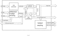
- An embodiment provides a CDMA security encoding system, the CDMA security coding system including a baseband signal generating device, a baseband encoding device, and a CDMA encoding device.
- the baseband signal generating device includes a D/A conversion unit, a differential bi-phase encoding unit, a conditioning and amplifying unit, a coupling unit, a re-collecting unit, a processing unit, a comparison unit, a control unit, a data monitoring unit, a display unit and an isolated sampling unit.
- an input terminal of the D/A conversion unit receives a first clock signal
- an output terminal of the D/A conversion unit communicates with an input terminal of the conditioning and amplifying unit
- an output terminal of the conditioning and amplifying unit communicates with an input terminal of the coupling unit.
- An input terminal of the differential bi-phase encoding unit receives a data signal and a second clock signal, and an output terminal of the differential bi-phase encoding unit communicates with the input terminal of the coupling unit.
- An output terminal of the coupling unit is configured to output a baseband signal.
- An input terminal of the data monitoring unit receives an output signal of the differential bi-phase encoding unit, and performs short-circuit protection on output signals of the differential bi-phase encoding unit and the D/A conversion unit, and an output terminal of the data monitoring unit sends monitoring information to the display unit.
- An input terminal of the re-collecting unit receives the output signal of differential bi-phase encoding unit, an output terminal of the re-collecting unit communicates with an input terminal of the processing unit, an output terminal of the processing unit communicates with an input terminal of the comparison unit, an output terminal of the comparison unit communicates with an input terminal of the control unit and the input terminal of the differential bi-phase encoding unit, and an output terminal of the control unit communicates with the input terminal of the differential bi-phase encoding unit.
- the isolated sampling unit communicates with the output terminal of the coupling unit, the isolated sampling unit includes a parallel step-down transformer and a series current transformer, the parallel step-down transformer performs voltage isolated sampling on a baseband signal output by the coupling unit, and the series current transformer performs current isolated sampling on the baseband signal output by the coupling unit.
- the baseband encoding device includes a disturbance unit, a data conversion unit, a scrambling unit, and a calculation unit; an input terminal of the disturbance unit receives the baseband signal, an output terminal of the disturbance unit communicates with an input terminal of the data conversion unit, an output terminal of the data conversion unit communicates with the input terminal of the scrambling unit, the output terminal of the scrambling unit communicates with an input terminal of the calculation unit, and an output terminal of the calculation unit is configured to output an encoded baseband signal.
- the CDMA encoding device includes a decoding unit, a differential modulation unit, a spread-spectrum modulation unit, a carrier modulation unit, a signal amplification and filtering unit, and a phase-locked loop unit.
- the decoding unit includes a differential bi-phase decoding unit and a Barker decoding unit;
- a first input terminal of the differential bi-phase decoding unit receives the encoded baseband signal
- an output terminal of the differential bi-phase decoding unit communicates with a first input terminal of the Barker decoding unit
- an output terminal of the Barker decoding unit communicates with a first input terminal of the differential modulation unit
- an output terminal of the differential modulation unit communicates with a first input terminal of the CDMA modulation module
- a first input terminal of the spread-spectrum code trigger module is configured to set a spread-spectrum code
- an output terminal of the spread-spectrum code trigger module communicates with a second input terminal of the CDMA modulation module.
- An output terminal of the CDMA modulation module communicates with a first input terminal of the BPSK modulation module, an output terminal of a carrier signal communicates with a second input terminal of the BPSK modulation module, and an output terminal of the BPSK modulation module is connected to an input terminal of a power amplifier, an output terminal of the power amplifier is connected with an input terminal of the filter, and an output terminal of the filter outputs the CDMA encoded signal.
- An input terminal of the phase-locked loop unit receives the encoded baseband signal, and the phase-locked loop unit has a plurality of output terminals; a first output terminal of the phase-locked loop unit communicates with a second input terminal of the differential bi-phase decoding unit, a second output terminal communicates with a second input terminal of the Barker decoding unit, a third output terminal of the phase-locked loop unit communicates with a second output terminal of the differential modulation unit and a second output terminal of the spread-spectrum code trigger module, and a fourth output terminal of the phase-locked loop unit communicates with a third input terminal of the spread-spectrum code trigger module.
- S1 the baseband signal generating device receives a digital signal to generate a baseband signal, as shown in FIG. 1
- the D/A conversion unit receives the first clock signal, the first clock signal exemplarily comes from a Field Programmable Gate Array (FPGA) module, the FPGA module is preferably placed in a functional module with double 2-out-of-2 comparison and security self-checking, and the D/A conversion unit converts the first clock signal to obtain the analog signal, and outputs the analog signal;
- the figured show that there are two first clock signals, the D/A conversion unit receives the two first clock signals, the D/A conversion module generates analog signals from the two received first clock signals by a digital counter, and specifically, the digital counter uses one of the first clock signals as a data signal, and the other first clock signal as a counting clock, and the digital counter performs mixed accumulation at an output terminal, and then generates the analog signals through operation-amplification processing; and the analog signals are transmitted to the coupling unit after undergoing a series of conditioning processing of the operation and amplification and push-pull of the conditioning and amplifying unit.
- FPGA Field Programmable Gate Array
- the differential bi-phase encoding unit receives the data signal and the second clock signal, the data signal exemplarily comes from a CPU unit, the CPU unit is preferably placed in the functional module with double 2-out-of-2 comparison and security self-checking, the second clock signal comes from the FPGA module as well, the differential bi-phase encoding is performed on the data signal to obtain the encoded digital signal, and the encoded digital signal is output;
- the drawings show that the differential bi-phase encoding unit receives four data signals for differential bi-phase encoding, and specifically, a JK flip-flop is configured to carry out differential bi-phase hardware encoding on the four data signals by twice the frequency of the data rate to obtain encoded digital signals and the encoded digital signals are transmitted to the coupling unit.
- the coupling unit receives an analog signal and an encoded digital signal, and performs coupling processing on the analog signal and the encoded digital signal to obtain a baseband signal, and specifically, two-in-one mixing and superposition are performed on the analog signal and the encoded digital signal by a synthetic transformer with a specific transformation ratio. Exemplarily, as shown in FIG.
- a first primary coil (input terminals 1 and 2) input analog signals
- a second primary coil (input terminals 3 and 5) input encoded digital signals
- a secondary coil outputs mixed and superimposed baseband signals
- the turns ratio of the first primary coil to the secondary coil is 35/92
- the turns ratio of the second primary coil to the secondary coil is 104/92 (that is, 26/23)
- the need of aliasing output of the signal amplitude of 14-18V and the signal amplitude of 20-23V is met, thereby generating a baseband signal complying with the European standard regulation, and exemplarily, bits of a baseband signal are 830 bits or 210 bits.
- an embodiment further uses the data monitoring unit to receive the encoded digital signal, and monitor the encoded digital signal, and the output of the analog signal and the encoded digital signal is cut off if a monitoring result shows that the encoded digital signal is a short-circuit signal, and specifically: the data monitoring unit monitors the encoded digital signal in manner of comparing the encoded digital signal with a preset threshold value, and if the encoded digital signal is greater than a preset threshold value, it indicates that the encoded digital signal is a short-circuit signal, at which time the data monitoring unit sends an alert message to the D/A conversion unit and the differential bi-phase encoding unit to facilitate the D/A conversion unit and the differential bi-phase encoding unit to cut off the output of the analog signal and the encoded digital signal, so as to implement the protection of the output signals of the differential bi-phase encoding unit and the D/A conversion unit, thereby guaranteeing security of an output signal of the coupling unit.
- the display unit receives the monitoring results of the data monitoring unit ( FIG. 2 shows that 8 monitoring results are received), and if a monitoring result shows that the encoded digital signal is a short-circuit signal, the display unit correspondingly displays a short-circuit state; and if a monitoring result shows that the encoded digital signal is an open-circuit signal, the display unit correspondingly displays an open-circuit state, and thus, it is convenient for an external staff to observe internal open and short-circuit states.
- an embodiment further uses the re-collecting unit to re-collect the encoded digital signal.
- the re-collecting unit re-collects 8 encoded digital signals
- the re-collecting unit transmits the 8 encoded digital signals to the processing unit
- the processing unit receives and decodes the re-collected encoded digital signals to obtain decoded digital signals
- the decoded digital signals are transmitted to the comparison unit
- the comparison unit compares the decoded digital signals with a data signal, if the decoded digital signals are consistent with the data signal, the encoded digital signals are output directly through the differential bi-phase encoding unit, and if the decoded digital signals are inconsistent with the data signal, the encoded digital signals are cut off under control of the control unit, and specifically, the control unit transmits four control signals to the differential bi-phase encoding unit, and the output of the encoded digital signals is cut off after the differential bi-phase encoding unit receives the control signals, further guaranteeing accuracy of the output signal of the
- an embodiment further uses the isolated sampling unit to perform isolated sampling of the baseband signal, and specifically, the isolated sampling unit is configured to perform voltage isolated sampling on the baseband signal of the coupling module through the parallel step-down transformer, and current isolated sampling through the series current transformer respectively, and abnormal output of baseband data is detected, thus guaranteeing effective output of data of the coupling unit.
- the disturbance unit receives the baseband signal (exemplary user data of 830bits or 210bits as shown in FIG. 4 ) and performs disturbance processing to obtain disturbed data and sends it to the data conversion unit; specifically, a 32-bit linear feedback shift register of a characteristic polynomial h (
- the data conversion unit receives the disturbed data and performs data conversion to obtain converted data, and sends it to the scrambling unit.
- the disturbed data is converted from 10bits to 11bits to obtain converted data of 913bits or 23 1bits; specifically, the disturbed data is grouped in the order of output by a codeword per 10bits, and then a pre-defined conversion table of 10bits to 11bits is used to perform data conversion on each codeword of 10bits from 10bits to 11bits.
- a conversion method is described as follows: a binary codeword of 10bits is represented by decimal x, then an x th 11bits data block is found out from the defined conversion table, and the 11bits data block is then a codeword of 11bits that is obtained after the conversion of the 10 bits codeword.
- the scrambling unit receives the converted data, and adds control bits and disturbance bits to the converted data to obtain scrambled data and sends it to the calculation unit.
- control bits are 3bits and the disturbance bits are 12bits.
- the calculation unit receives the scrambled data, selects additional trimming bits that meet the conditions, calculates check bits, and then adds the additional trimming bits and the check bits to the scrambled data to obtain an encoded baseband signal with specific bits, and exemplarily, the additional trimming bits are 10bits, the check bits are 85bits, and the bits of the encoded baseband signal are 1023bits or 341bits.
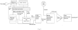
- S3 the CDMA encoding device performs CDMA encoding on the encoded baseband signal to obtain a CDMA encoded signal, as shown in FIG. 5 , which includes: S3-1: decoding the encoded baseband signal (that is, the user data in FIG. 5 ) to obtain the baseband decoded signal, specifically as follows:
- the first input terminal of the differential bi-phase decoding unit receives the encoded baseband signal, performs differential bi-phase decoding on the encoded baseband signal to obtain the initial decoded signal, and exemplarily, the differential bi-phase decoding unit performs Differential Bi-Phase Level (DBPL) decoding on the encoded baseband signal to obtain the initial decoded signal.
- DBPL Differential Bi-Phase Level
- the first input terminal of the Barker decoding unit receives the initial decoded signal, and performs Barker decoding on the initial decoded signal to obtain a baseband decoded signal (indicated as binary data in FIG. 5 ), and exemplarily, the Barker decoding unit converts the initial decoded signal into a Barker code 11100010010 of a 11-bit chip, then the Barker code 11100010010 of the 11-bit chip is demodulated to logic 1, and an inverse code of the Barker code of the 11-bit chip is demodulated to logic 0 to obtain a baseband decoded signal.
- modulation is performed on the baseband decoded signal, the modulation including differential modulation, spread-spectrum modulation and carrier modulation sequentially, and finally the carrier frequency signal is acquired, which is specifically described as follows:
- the first input terminal of the CDMA modulation module receives the differential modulated signal, and its second input terminal receives the address code, and direct sequence spread-spectrum modulation is performed on the differential modulation signal and the address code to obtain a spread-spectrum modulated signal (that is, a modulation chip in FIG. 5 ), and the spread-spectrum modulated signal is transmitted to the BPSK modulation module.
- a spread-spectrum modulated signal that is, a modulation chip in FIG. 5
- the carrier modulation unit performs carrier modulation on the spread-spectrum modulated signal to obtain a carrier frequency signal; specifically: The carrier signal source generates a carrier for carrier modulation, and the carrier is sent to the BPSK modulation module.
- the BPSK modulation module receives the carrier and the spread-spectrum modulated signal for carrier modulation, so that the spread-spectrum modulated signal is spread by N times to obtain a carrier frequency signal (that is, the CDMA signal in FIG. 5 ).
- the BPSK modulation module uses the carrier to spread the spread-spectrum modulated signal by 3 times to generate a carrier frequency signal of 13.545 MHz.
- the signal amplification and filtering unit performs amplification and filtering processing on the carrier frequency signal, specifically, The power amplifier performs amplification processing on the carrier frequency signal without power distortion, and then transmits an amplified signal to the filter, and the filter receives the amplified signal for filtering processing to guarantee the transmission quality of the carrier frequency signal, that is, the bit error rate is less than 10 -5 , undesired amplitude modulation is not greater than 7%, etc., and finally the CDMA encoded signal is obtained, that is, the CDMA encoded signal (that is, a loop line signal in FIG. 5 ) that conforms to the system of a signal that is received by the loop line transmission module of the European train operation control system.
- the CDMA encoded signal that is, a loop line signal in FIG. 5
- this embodiment further uses the phase-locked loop unit to guarantee the synchronization of encoded baseband signal processing, specifically, the input terminal of the phase-locked loop unit is configured to receive the encoded baseband signal.
- the first output terminal of the phase-locked loop unit outputs a signal to the second input terminal of the differential bi-phase decoding unit
- the second output terminal of the phase-locked loop unit outputs a signal to the second input terminal of the Barker decoding unit
- the third output terminal of the phase-locked loop unit outputs a signal to the second output terminal of the differential modulation unit and the second output terminal of the spread-spectrum code trigger module
- the fourth output terminal of the phase-locked loop unit outputs a signal to the third input terminal of the spread-spectrum code trigger module, thereby controlling the phase and frequency in the related signal processing processes of the differential bi-phase decoding unit, the Barker decoding unit, the differential modulation unit and the spread-spectrum code trigger module to kept synchronized with those of the input encoded baseband signal.
- this embodiment further provides a CDMA decoding system and decoding method.
- a decoded spread-spectrum code is transmitted to the loop line transmission module through an air interface in a signal system different from FSK through an European standard transponder of a signal device, and the loop line transmission module performs CDMA decoding with the decoded spread-spectrum code, and exemplarily, the European standard transponder used in this embodiment is a downsized European standard transponder that complies with ss-036.
- the CDMA decoding unit includes a Band-Pass Filter (BPF), an A/D module, a digital down-conversion module, a baseband signal interference processing module, and a demodulation module, the digital down-conversion module including a Low-Pass Filter (LPF) and a sampling module.
- BPF Band-Pass Filter
- A/D A/D
- digital down-conversion module a baseband signal interference processing module
- LPF Low-Pass Filter
- the CDMA decoding method specifically includes: Receiving the CDMA encoded signal (that is, r(t) in FIG. 6 ) by the band-pass filter, performing out-of-band noise and interference signal suppression on the CDMA encoded signal, and then transmitting the filtered signal to the A/D module.
- the A/D module realizes mid-band pass sampling, acquires the intermediate frequency digital signal and transmits it to the digital down-conversion module; wherein, the A/D module uses a 108.38 MHz crystal for sampling, with a bit width of 14bits, and the sampling rate is 8 times that of the CDMA carrier signal, which can adapt to signal scenarios with large DC offset and high dynamic range.
- the digital down-conversion module receives the intermediate frequency digital signal and down-converts the intermediate frequency signal to the baseband signal, that is, the carrier frequency of the intermediate frequency signal is removed to be restored into the CDMA encoded baseband signal.
- interference processing is performed on the intermediate frequency digital signal to reduce carrier synchronization and code capture errors.
- the interference processing of the intermediate frequency signal is realized in the digital down-conversion module, specifically the intermediate frequency digital signal is made to pass through the low-pass filter, and the low-pass filter has a flat passband characteristic and a group delay characteristic, so that a target signal can pass through the low-pass filter without distortion, and meanwhile, it has a very steep transition band, so that very good adjacent channel suppression capability can be provided.
- the typical adjacent channel suppression capability range of the low-pass filter is 30-90dB, and the intermediate frequency digital signal suppressed by the low-pass filter is sampled by the sampling module to be restored to the CDMA encoded baseband signal.
- this embodiment divides the intermediate frequency digital signal into two channels for interference processing, that is, the interference processing of the intermediate frequency signal is realized through a channel I and a channel Q respectively, so as to avoid that when one of the channels fails, the other channel can perform interference processing operation of the intermediate frequency signal normally.
- the baseband signal interference processing module eliminates possible adjacent channel interference and single-tone interference signals and the like of the European loop line from the CDMA encoded baseband signal to filter out a down-converted folding frequency component.
- the demodulation module restores the CDMA encoded baseband signal according to the known address spread-spectrum code number to obtain the CDMA decoded signal, and the drawings show use of a BPSK demodulation mode.
Landscapes
- Engineering & Computer Science (AREA)
- Computer Networks & Wireless Communication (AREA)
- Signal Processing (AREA)
- Digital Transmission Methods That Use Modulated Carrier Waves (AREA)
Claims (12)
- CDMA-Sicherheitscodierungsverfahren, umfassend die Schritte:Empfangen eines ersten Taktsignals und Umwandeln des ersten Taktsignals in ein analoges Signal;Empfangen eines Datensignals und eines zweiten Taktsignals, und Durchführen einer differenziellen Bi-Phasencodierung an dem Datensignal, um ein codiertes digitales Signal zu erhalten;nach dem Aufbereiten und Verstärken des analogen Signals, Koppeln des analogen Signals mit dem codierten digitalen Signal, um ein gewünschtes Basisbandsignal zu erhalten, wobei eine Zweiin-Eins-Mischung und Überlagerung des analogen Signals und des codierten digitalen Signals durch einen synthetischen Transformator mit einem spezifischen Transformationsverhältnis durchgeführt wird;Codieren des Basisbandsignals, um ein codiertes Basisbandsignal zu erhalten, wobei eine Störeinheit das Basisbandsignal empfängt und eine Störungsverarbeitung durchführt, um gestörte Daten zu erhalten, und sie an eine Datenumwandlungseinheit sendet, die Datenumwandlungseinheit die gestörten Daten empfängt und eine Datenumwandlung durchführt, um umgewandelte Daten zu erhalten, und sie an eine Verwürfelungseinheit sendet, die Verwürfelungseinheit die umgewandelten Daten empfängt und Steuerbits und Störungsbits zu den umgewandelten Daten addiert, um verwürfelte Daten zu erhalten, und die verwürfelten Daten an eine Berechnungseinheit sendet; die Berechnungseinheit die verwürfelten Daten empfängt, zusätzliche Trimm-Bits auswählt, die bestimmte Bedingungen erfüllen, Prüfbits berechnet und dann die zusätzlichen Trimm-Bits und die Prüfbits zu den verwürfelten Daten addiert, um ein codiertes Basisbandsignal mit bestimmten Bits zu erhalten;
undDurchführen einer CDMA-Codierung auf dem codierten Basisbandsignal, um ein codiertes CDMA-Signal zu erhalten. - CDMA-Sicherheitscodierungsverfahren nach Anspruch 1, ferner umfassend die folgenden Schritte:Wiedereinsammeln des codierten digitalen Signals;Decodieren des wiedergesammelten codierten digitalen Signals, um ein decodiertes digitales Signal zu erhalten;Vergleichen des decodierten digitalen Signals mit dem Datensignal und Unterbrechen der Ausgabe des codierten digitalen Signals, wenn das decodierte digitale Signal mit dem Datensignal nicht konsistent ist; undAusgabe des codierten Digitalsignals, wenn das decodierte Digitalsignal mit dem Datensignal konsistent ist.
- CDMA-Sicherheitscodierungsverfahren nach Anspruch 1, das vor dem Empfangen des analogen Signals und des codierten digitalen Signals und dem Durchführen der Kopplungsverarbeitung des analogen Signals und des codierten digitalen Signals die folgenden Schritte umfasst:
Empfangen des codierten digitalen Signals, Überwachen des codierten digitalen Signals und Abschalten des Ausgangs des analogen Signals und des codierten digitalen Signals, wenn ein Überwachungsergebnis zeigt, dass das codierte digitale Signal ein Kurzschlusssignal ist. - CDMA-Sicherheitscodierungsverfahren nach Anspruch 1, wobei das Durchführen der CDMA-Codierung des codierten Basisbandsignals zum Erhalt eines CDMA-codierten Signals insbesondere die folgenden Schritte umfasst:sequentielles Durchführen einer differentiellen Zweiphasen-Decodierung und einer Barker-Decodierung an dem codierten Basisbandsignal, um ein decodiertes Basisbandsignal zu erhalten;Durchführen einer Differenzmodulation auf dem Basisbanddecodierten Signal, um ein differenziell moduliertes Signal zu erhalten;Erzeugen eines Adresscodes für die Spreizspektrummodulation, und Durchführen einer Direktsequenz-Spreizspektrummodulation an dem differenziell modulierten Signal und dem Adresscode, um ein spreizspektrummoduliertes Signal zu erhalten;Erzeugen eines Trägers zur Trägermodulation und Durchführen einer Trägermodulation an dem spreizspektrummodulierten Signal und dem Träger, sodass das spreizspektrummodulierte Signal um das N-fache gespreizt wird, um ein Trägerfrequenzsignal zu erhalten; undDurchführen von Leistungsverstärkung und Filterung des Trägerfrequenzsignals, um ein CDMA-codiertes Signal zu erhalten.
- CDMA-Sicherheitscodierungsverfahren nach Anspruch 4, das ferner Folgendes umfasst:Empfangen des codierten Basisbandsignals durch eine phasenstarre Schleife; undSteuern der Frequenz und der Phase in den Prozessen der differentiellen Zweiphasen-Decodierung, der Barker-Decodierung, der differentiellen Modulation und der Adresscode-Erzeugung entsprechend dem codierten Basisbandsignal durch den Phasenregelkreis, um sie mit denen des codierten Basisbandsignals zu synchronisieren.
- CDMA-Sicherheitscodierungssystem, das eine Basisbandsignalerzeugungsvorrichtung, eine Basisbandcodierungsvorrichtung und eine CDMA-Codierungsvorrichtung umfasst; wobei die Basisbandsignalerzeugungsvorrichtung eine D/A-Wandlereinheit, eine differentielle Zweiphasen-Codierungseinheit, eine Aufbereitungs- und Verstärkungseinheit und eine Kopplungseinheit umfasst;wobei die D/A-Wandlereinheit so konfiguriert ist, dass sie das erste Taktsignal empfängt und das erste Taktsignal umwandelt, um ein analoges Signal zu erhalten;wobei die differentielle Zweiphasen-Codierungseinheit so konfiguriert ist, dass sie das Datensignal und das zweite Taktsignal empfängt und eine differentielle Zweiphasen-Codierung an dem Datensignal durchführt, um ein codiertes digitales Signal zu erhalten;wobei die Konditionierungs- und Verstärkungseinheit so konfiguriert ist, dass sie eine Konditionierung und Verstärkung des Analogsignals durchführt, um ein konditioniertes verstärktes Analogsignal zu erhalten;wobei die Kopplungseinheit so konfiguriert ist, dass sie eine Kopplungsverarbeitung des konditionierten und verstärkten analogen Signals und des codierten digitalen Signals durchführt, um ein gewünschtes Basisbandsignal zu erhalten, wobei eine Zweiin-Eins-Mischung und Überlagerung des analogen Signals und des codierten digitalen Signals durch einen synthetischen Transformator mit einem spezifischen Transformationsverhältnis durchgeführt wird;die Basisband-Codierungsvorrichtung so konfiguriert ist, dass sie das Basisbandsignal codiert, um ein codiertes Basisbandsignal zu erhalten, und eine Störeinheit, eine Datenumwandlungseinheit, eine Verschlüsselungseinheit und eine Berechnungseinheit enthält, wobei die Störeinheit so konfiguriert ist, dass sie das Basisbandsignal empfängt und eine Störungsverarbeitung durchführt, um gestörte Daten zu erhalten und sie an die Datenumwandlungseinheit zu senden, die Datenumwandlungseinheit so konfiguriert ist, dass sie die gestörten Daten empfängt und eine Datenumwandlung durchführt, um umgewandelte Daten zu erhalten, und diese an die Verwürfelungseinheit sendet, die Verwürfelungseinheit so konfiguriert ist, dass sie die umgewandelten Daten empfängt und Steuerbits und Störungsbits zu den umgewandelten Daten hinzufügt, um verwürfelte Daten zu erhalten, und die verwürfelten Daten an die Berechnungseinheit sendet; die Berechnungseinheit so konfiguriert ist, dass sie die verwürfelten Daten empfängt, zusätzliche Trimm-Bits auswählt, die spezifische Bedingungen erfüllen, Prüfbits berechnet und dann die zusätzlichen Trimm-Bits und die Prüfbits zu den verwürfelten Daten addiert, um ein codiertes Basisbandsignal mit spezifischen Bits zu erhalten; undwobei die CDMA-Codierungsvorrichtung so konfiguriert ist, dass sie eine CDMA-Codierung an dem codierten Basisbandsignal durchführt, um ein CDMA-codiertes Signal zu erhalten.
- CDMA-Sicherheitscodierungssystem nach Anspruch 6, wobei die Basisbandsignal-Erzeugungsvorrichtung ferner eine Rekollektionseinheit, eine Verarbeitungseinheit, eine Vergleichseinheit und eine Steuereinheit umfasst;wobei die Rekollektionseinheit dazu konfiguriert ist, ein codiertes digitales Signal erneut zu sammeln;wobei die Verarbeitungseinheit so konfiguriert ist, dass sie das neu gesammelte codierte digitale Signal decodiert, um ein decodiertes digitales Signal zu erhalten;wobei die Vergleichseinheit so konfiguriert ist, dass sie das decodierte digitale Signal mit dem Datensignal vergleicht, und die Ausgabe des codierten digitalen Signals unter Steuerung der Steuereinheit abgeschnitten wird, wenn das decodierte digitale Signal nicht mit dem Datensignal übereinstimmt; undwobei das codierte digitale Signal über die differentielle Zweiphasen-Codierungseinheit ausgegeben wird, wenn das decodierte digitale Signal mit dem Datensignal übereinstimmt.
- CDMA-Sicherheitscodierungssystem nach Anspruch 6, wobei die Basisbandsignal-Erzeugungsvorrichtung ferner eine Datenüberwachungseinheit umfasst; und bevor die Kopplungseinheit eine Kopplungsverarbeitung an dem konditionierten verstärkten Analogsignal und dem codierten Digitalsignal durchführt, um ein Basisbandsignal zu erhalten,
wobei die Datenüberwachungseinheit das codierte digitale Signal empfängt und das codierte digitale Signal überwacht und die Ausgabe des analogen Signals und des codierten digitalen Signals unterbrochen wird, wenn ein Überwachungsergebnis zeigt, dass das codierte digitale Signal ein Kurzschlusssignal ist. - CDMA-Sicherheitscodierungssystem nach Anspruch 6, wobei die CDMA-Codierungsvorrichtung eine differentielle Zweiphasen-Decodierungseinheit, eine Barker-Decodierungseinheit, eine differentielle Modulationseinheit, eine Spreizspektrummodulationseinheit, eine Trägermodulationseinheit und eine Signalverstärkungs- und -filterungseinheit umfasst;die Spreizspektrummodulationseinheit ein Spreizspektrumscode-Triggermodul und ein CDMA-Modulationsmodul umfasst;wobei die Trägermodulationseinheit eine Trägersignalquelle und ein BPSK-Modulationsmodul umfasst;wobei die differentielle Zweiphasen-Decodierungseinheit eine differentielle Zweiphasen-Decodierung des codierten Basisbandsignals durchführt, um ein erstes decodiertes Signal zu erhalten;wobei die Barker-Decodierungseinheit so konfiguriert ist, dass sie eine Barker-Decodierung an dem anfänglich decodierten Signal durchführt, um ein decodiertes Basisbandsignal zu erhalten;wobei die Differenzmodulationseinheit so konfiguriert ist, dass sie eine Differenzmodulation an dem decodierten Basisbandsignal durchführt, um ein differenzmoduliertes Signal zu erhalten;wobei das Spreizspektrumscode-Triggermodul so konfiguriert ist, dass es einen Adresscode für die Spreizspektrummodulation erzeugt;wobei das CDMA-Modulationsmodul so konfiguriert ist, dass es eine Direktsequenz-Spreizspektrummodulation an dem differenziell modulierten Signal und dem Adresscode durchführt, um ein spreizspektrummoduliertes Signal zu erhalten;wobei die Trägersignalquelle so konfiguriert ist, dass sie einen Träger für die Trägermodulation erzeugt;wobei das BPSK-Modulationsmodul so konfiguriert ist, dass es eine Trägermodulation an dem spreizspektrummodulierten Signal und dem Träger durchführt, sodass das spreizspektrummodulierte Signal um das N-fache gespreizt wird, um ein Trägerfrequenzsignal zu erhalten; undwobei die Signalverstärkungs- und -filterungseinheit so konfiguriert ist, dass sie das Trägerfrequenzsignal verstärkt und filtert, um ein CDMA-codiertes Signal zu erhalten.
- CDMA-Sicherheitscodierungssystem nach Anspruch 9, wobei die CDMA-Codierungseinheit ferner eine Phasenregelkreiseinheit umfasst;
wobei die Phasenregelkreiseinheit so konfiguriert ist, dass sie das codierte Basisbandsignal empfängt und die Frequenz und Phase in den Prozessen der differentiellen Zweiphasen-Decodierung, der Barker-Decodierung, der differentiellen Modulation und der Adresscode-Erzeugung entsprechend dem codierten Basisbandsignal so steuert, dass sie mit denen des codierten Basisbandsignals synchronisiert sind. - CDMA-Sicherheitscodierungs- und -decodierungsverfahren, das das CDMA-Sicherheitscodierungsverfahren nach Anspruch 1 umfasst, das die folgenden Schritte umfasst:Empfangen des CDMA-codierten Signals mittels eines Bandpassfilters und Durchführen einer Filterverarbeitung des CDMA-codierten Signals, um ein gefiltertes Signal zu erhalten;Empfangen des gefilterten Signals durch ein A/D-Modul und Durchführen einer Mittelbandpassabtastung des gefilterten Signals, um ein digitales Zwischenfrequenzsignal zu erhalten;Empfangen des digitalen Zwischenfrequenzsignals durch ein digitales Abwärtswandlungsmodul, Abwärtswandeln des Zwischenfrequenzsignals in ein Basisbandsignal und Durchführen einer Interferenzverarbeitung an dem Zwischenfrequenzsignal, um ein CDMA-codiertes Basisbandsignal zu erhalten;Empfangen des CDMA-codierten Basisbandsignals durch ein Basisbandsignal-Interferenzverarbeitungsmodul und Eliminieren eines Nachbarkanals und eines Ein-Ton-Interferenzsignals in dem CDMA-codierten Basisbandsignal, um ein verarbeitetes CDMA-codiertes Basisbandsignal zu erhalten; undEmpfangen des verarbeiteten CDMA-codierten Basisbandsignals durch ein Demodulationsmodul und Wiederherstellen des verarbeiteten CDMA-codierten Basisbandsignals gemäß einer bekannten Adressspreizspektrum-Codenummer, um ein CDMAdecodiertes Signal zu erhalten.
- CDMA-Sicherheitscodier- und -Decodierungssystem mit dem CDMA-Sicherheitscodierungssystem nach Anspruch 6, ferner umfassend einen Bandpassfilter, ein A/D-Modul, ein digitales Abwärtswandlungsmodul, ein Basisbandsignal-Interferenzverarbeitungsmodul und ein Demodulationsmodul, und ein digitales Abwärtswandlungsmodul; wobeider Bandpassfilter so konfiguriert ist, dass er das CDMA-codierte Signal empfängt und Außerbandrauschen und ein Störsignal in dem CDMA-codierten Signal unterdrückt, um ein gefiltertes Signal zu erhalten;das A/D-Modul so konfiguriert ist, dass es das gefilterte Signal empfängt und eine Mittelbandpassabtastung des gefilterten Signals durchführt, um ein digitales Zwischenfrequenzsignal zu erhalten;das digitale Abwärtswandlungsmodul so konfiguriert ist, dass es das digitale Zwischenfrequenzsignal empfängt, das Zwischenfrequenzsignal in ein Basisbandsignal abwärts wandelt und eine Interferenzverarbeitung an dem Zwischenfrequenzsignal durchführt, um ein CDMA-codiertes Basisbandsignal zu erhalten;das Basisbandsignal-Interferenzverarbeitungsmodul so konfiguriert ist, dass es das CDMA-codierte Basisbandsignal empfängt und einen Nachbarkanal und ein Einzelton-Interferenzsignal eliminiert, um ein verarbeitetes CDMA-codiertes Basisbandsignal zu erhalten; unddas Demodulationsmodul so konfiguriert ist, dass es das verarbeitete CDMA-codierte Basisbandsignal empfängt und das verarbeitete CDMA-codierte Basisbandsignal gemäß der bekannten Adressspreizspektrum-Codenummer wiederherstellt, um ein CDMAdecodiertes Signal zu erhalten.
Priority Applications (1)
| Application Number | Priority Date | Filing Date | Title |
|---|---|---|---|
| RS20241321A RS66224B1 (sr) | 2021-06-17 | 2021-07-08 | Postupak i sistem cdma bezbednosnog kodiranјa, i postupak i sistem cdma bezbednosnog dekodiranјa |
Applications Claiming Priority (2)
| Application Number | Priority Date | Filing Date | Title |
|---|---|---|---|
| CN202110668883.3A CN113131967B (zh) | 2021-06-17 | 2021-06-17 | Cdma安全编码、解码方法及系统 |
| PCT/CN2021/105123 WO2022262023A1 (zh) | 2021-06-17 | 2021-07-08 | Cdma安全编码、解码方法及系统 |
Publications (4)
| Publication Number | Publication Date |
|---|---|
| EP4131789A1 EP4131789A1 (de) | 2023-02-08 |
| EP4131789A4 EP4131789A4 (de) | 2023-09-20 |
| EP4131789B1 true EP4131789B1 (de) | 2024-10-30 |
| EP4131789C0 EP4131789C0 (de) | 2024-10-30 |
Family
ID=76782992
Family Applications (1)
| Application Number | Title | Priority Date | Filing Date |
|---|---|---|---|
| EP21751949.5A Active EP4131789B1 (de) | 2021-06-17 | 2021-07-08 | Sicheres cdma-codierungsverfahren und -system sowie sicheres cdma-decodierungsverfahren und -system |
Country Status (5)
| Country | Link |
|---|---|
| EP (1) | EP4131789B1 (de) |
| CN (1) | CN113131967B (de) |
| HU (1) | HUE069504T2 (de) |
| RS (1) | RS66224B1 (de) |
| WO (1) | WO2022262023A1 (de) |
Families Citing this family (5)
| Publication number | Priority date | Publication date | Assignee | Title |
|---|---|---|---|---|
| CN114531178B (zh) * | 2022-01-28 | 2023-03-21 | 珠海昇生微电子有限责任公司 | 一种充电及双向通讯系统与方法 |
| CN115454460B (zh) * | 2022-10-21 | 2025-12-02 | 无锡翼盟电子科技有限公司 | 一种打印机耗材芯片数据无线更新装置 |
| CN115469897B (zh) * | 2022-10-21 | 2025-12-02 | 无锡翼盟电子科技有限公司 | 一种基于霍尔传感器的打印机耗材芯片数据更新装置 |
| CN117439618A (zh) * | 2023-08-31 | 2024-01-23 | 广州市广源电子科技有限公司 | 基于gsmr网络的铁路fsk信号发送系统及其高可靠传输方法 |
| CN119030646A (zh) * | 2024-10-17 | 2024-11-26 | 芯百特微电子(无锡)有限公司 | 基于数据分析的cdma通信模组测试数据分析方法 |
Family Cites Families (12)
| Publication number | Priority date | Publication date | Assignee | Title |
|---|---|---|---|---|
| US5377226A (en) * | 1993-10-19 | 1994-12-27 | Hughes Aircraft Company | Fractionally-spaced equalizer for a DS-CDMA system |
| US6272121B1 (en) * | 1997-03-03 | 2001-08-07 | Omnipoint Corporation | Spread spectrum communication system using DECT protocol |
| US7280607B2 (en) * | 1997-12-12 | 2007-10-09 | Freescale Semiconductor, Inc. | Ultra wide bandwidth communications method and system |
| TWI234374B (en) * | 2003-03-04 | 2005-06-11 | Realtek Semiconductor Corp | Spread spectrum encoding method and spread spectrum encoding modulation method |
| US9217653B2 (en) * | 2007-09-13 | 2015-12-22 | Rosemount Inc. | High performance architecture for process transmitters |
| CN101505184B (zh) * | 2009-02-27 | 2012-07-25 | 中国电子科技集团公司第五十四研究所 | 隐蔽卫星通信终端 |
| CN101969421B (zh) * | 2010-09-19 | 2013-03-06 | 福建邮科通信技术有限公司 | 采用五类线传送cdma信号的装置 |
| US9425854B2 (en) * | 2012-06-18 | 2016-08-23 | Alstom Transport Technologies | Spread spectrum signals in vehicle network systems |
| CN106157588B (zh) * | 2016-08-15 | 2022-04-29 | 扬州恒隆软件有限公司 | 快速高精度光电直读式智能水表系统 |
| CN108418603A (zh) * | 2018-05-08 | 2018-08-17 | 北京凤凰汇通科技有限公司 | 用于铁路的地面无线扩频通信系统 |
| US10530618B1 (en) * | 2018-09-26 | 2020-01-07 | Qualcomm Incorporated | Single-ended to differential signal conversion of analog signals |
| CN110007325B (zh) * | 2019-04-15 | 2022-09-13 | 中国电子科技集团公司第二十研究所 | 一种用于星基增强l5信号的快速帧同步方法 |
-
2021
- 2021-06-17 CN CN202110668883.3A patent/CN113131967B/zh active Active
- 2021-07-08 RS RS20241321A patent/RS66224B1/sr unknown
- 2021-07-08 EP EP21751949.5A patent/EP4131789B1/de active Active
- 2021-07-08 HU HUE21751949A patent/HUE069504T2/hu unknown
- 2021-07-08 WO PCT/CN2021/105123 patent/WO2022262023A1/zh not_active Ceased
Also Published As
| Publication number | Publication date |
|---|---|
| HUE069504T2 (hu) | 2025-03-28 |
| RS66224B1 (sr) | 2024-12-31 |
| EP4131789A1 (de) | 2023-02-08 |
| WO2022262023A1 (zh) | 2022-12-22 |
| CN113131967A (zh) | 2021-07-16 |
| CN113131967B (zh) | 2021-08-31 |
| EP4131789A4 (de) | 2023-09-20 |
| EP4131789C0 (de) | 2024-10-30 |
Similar Documents
| Publication | Publication Date | Title |
|---|---|---|
| EP4131789B1 (de) | Sicheres cdma-codierungsverfahren und -system sowie sicheres cdma-decodierungsverfahren und -system | |
| US5432815A (en) | Data modulator-demodulator apparatus of a spread spectrum communication system | |
| EP2975814B1 (de) | Chirpsignalprozessor | |
| US10270488B2 (en) | Binary high-power modulator | |
| EA031912B1 (ru) | Комбинированная амплитудно-временная и фазовая модуляция | |
| CN108988906B (zh) | 一种数据速率可变的非相干扩频通信装置 | |
| KR100528891B1 (ko) | 코딩된 출력 신호를 생성하는 방법 및 디코딩된 데이터스트림을 생성하는 방법 | |
| CN110995334B (zh) | 一种多通道并行处理的天基跳频数据链系统 | |
| CN104661287A (zh) | 一种支持多模的并行多通道快速扫频方法及系统 | |
| US11387864B2 (en) | Pulse based wideband signaling | |
| US5388126A (en) | Baseband signal processor for a microwave radio receiver | |
| EP2524441B1 (de) | Vorrichtung und verfahren zur ultrabreitband-kommunikation | |
| US20050163235A1 (en) | Method and apparatus for improving error rates in multi-band ultra wideband communication systems | |
| EP1585229B1 (de) | FSK mit versetzten Frequenzen | |
| CN101505184A (zh) | 隐蔽卫星通信终端 | |
| JP6033427B2 (ja) | 複数のメッセージシンボルの無線伝送のための方法、システム、および、システムのための受信器 | |
| CN110071739B (zh) | 一种基于跳频、gmsk和ds的通信系统及方法 | |
| US7542526B2 (en) | Integer cycle event detection using wavelet pass filter system and method | |
| CN108206701B (zh) | 宽带射频发送装置、接收装置、发送方法与接收方法 | |
| CN116418365A (zh) | 一种基于带内跳频体制的调制解调装置 | |
| US20070140317A1 (en) | Differential phase modulated multi-band ultra-wideband communication system | |
| EP1532825A1 (de) | Kostengünstige hochleistungfähige digitale schnurlose telefon-architektur | |
| Souilmi et al. | Challenges in UWB signaling for adhoc networking | |
| CN115765887B (zh) | 一种跳频联合直接序列扩频的水声调制解调方法 | |
| Nikitin et al. | Utilizing pulse pileup effect in development of robust low-SNR covert communication links |
Legal Events
| Date | Code | Title | Description |
|---|---|---|---|
| STAA | Information on the status of an ep patent application or granted ep patent |
Free format text: STATUS: UNKNOWN |
|
| STAA | Information on the status of an ep patent application or granted ep patent |
Free format text: STATUS: THE INTERNATIONAL PUBLICATION HAS BEEN MADE |
|
| PUAI | Public reference made under article 153(3) epc to a published international application that has entered the european phase |
Free format text: ORIGINAL CODE: 0009012 |
|
| STAA | Information on the status of an ep patent application or granted ep patent |
Free format text: STATUS: REQUEST FOR EXAMINATION WAS MADE |
|
| 17P | Request for examination filed |
Effective date: 20210818 |
|
| AK | Designated contracting states |
Kind code of ref document: A1 Designated state(s): AL AT BE BG CH CY CZ DE DK EE ES FI FR GB GR HR HU IE IS IT LI LT LU LV MC MK MT NL NO PL PT RO RS SE SI SK SM TR |
|
| RIN1 | Information on inventor provided before grant (corrected) |
Inventor name: XU, YANWEN Inventor name: CHEN, GUANG Inventor name: DING, HUAN Inventor name: ZHANG, SHENGWEN Inventor name: LV, XIANLIANG Inventor name: SUN, ZHENYU Inventor name: LI, XUEJIAN Inventor name: ZHANG, FUSONG Inventor name: SUN, GUOYING Inventor name: YE, FENG Inventor name: YANG, GUANGLUN Inventor name: WANG, GUOYING |
|
| A4 | Supplementary search report drawn up and despatched |
Effective date: 20230821 |
|
| RIC1 | Information provided on ipc code assigned before grant |
Ipc: H04B 1/40 20150101ALN20230814BHEP Ipc: H04K 1/02 20060101ALI20230814BHEP Ipc: H04B 1/3822 20150101ALI20230814BHEP Ipc: H04B 1/7097 20110101ALI20230814BHEP Ipc: H04B 1/7073 20110101ALI20230814BHEP Ipc: H04B 1/707 20110101AFI20230814BHEP |
|
| RIC1 | Information provided on ipc code assigned before grant |
Ipc: H04B 1/40 20150101ALN20240430BHEP Ipc: H04K 1/02 20060101ALI20240430BHEP Ipc: H04B 1/3822 20150101ALI20240430BHEP Ipc: H04B 1/7097 20110101ALI20240430BHEP Ipc: H04B 1/7073 20110101ALI20240430BHEP Ipc: H04B 1/707 20110101AFI20240430BHEP |
|
| GRAP | Despatch of communication of intention to grant a patent |
Free format text: ORIGINAL CODE: EPIDOSNIGR1 |
|
| STAA | Information on the status of an ep patent application or granted ep patent |
Free format text: STATUS: GRANT OF PATENT IS INTENDED |
|
| DAV | Request for validation of the european patent (deleted) | ||
| DAX | Request for extension of the european patent (deleted) | ||
| INTG | Intention to grant announced |
Effective date: 20240607 |
|
| GRAS | Grant fee paid |
Free format text: ORIGINAL CODE: EPIDOSNIGR3 |
|
| GRAA | (expected) grant |
Free format text: ORIGINAL CODE: 0009210 |
|
| STAA | Information on the status of an ep patent application or granted ep patent |
Free format text: STATUS: THE PATENT HAS BEEN GRANTED |
|
| AK | Designated contracting states |
Kind code of ref document: B1 Designated state(s): AL AT BE BG CH CY CZ DE DK EE ES FI FR GB GR HR HU IE IS IT LI LT LU LV MC MK MT NL NO PL PT RO RS SE SI SK SM TR |
|
| REG | Reference to a national code |
Ref country code: GB Ref legal event code: FG4D |
|
| REG | Reference to a national code |
Ref country code: CH Ref legal event code: EP |
|
| REG | Reference to a national code |
Ref country code: DE Ref legal event code: R096 Ref document number: 602021021051 Country of ref document: DE |
|
| REG | Reference to a national code |
Ref country code: IE Ref legal event code: FG4D |
|
| U01 | Request for unitary effect filed |
Effective date: 20241104 |
|
| U07 | Unitary effect registered |
Designated state(s): AT BE BG DE DK EE FI FR IT LT LU LV MT NL PT RO SE SI Effective date: 20241114 |
|
| REG | Reference to a national code |
Ref country code: SK Ref legal event code: T3 Ref document number: E 45393 Country of ref document: SK |
|
| REG | Reference to a national code |
Ref country code: HU Ref legal event code: AG4A Ref document number: E069504 Country of ref document: HU |
|
| PG25 | Lapsed in a contracting state [announced via postgrant information from national office to epo] |
Ref country code: IS Free format text: LAPSE BECAUSE OF FAILURE TO SUBMIT A TRANSLATION OF THE DESCRIPTION OR TO PAY THE FEE WITHIN THE PRESCRIBED TIME-LIMIT Effective date: 20250228 Ref country code: HR Free format text: LAPSE BECAUSE OF FAILURE TO SUBMIT A TRANSLATION OF THE DESCRIPTION OR TO PAY THE FEE WITHIN THE PRESCRIBED TIME-LIMIT Effective date: 20241030 |
|
| PG25 | Lapsed in a contracting state [announced via postgrant information from national office to epo] |
Ref country code: ES Free format text: LAPSE BECAUSE OF FAILURE TO SUBMIT A TRANSLATION OF THE DESCRIPTION OR TO PAY THE FEE WITHIN THE PRESCRIBED TIME-LIMIT Effective date: 20241030 |
|
| PG25 | Lapsed in a contracting state [announced via postgrant information from national office to epo] |
Ref country code: NO Free format text: LAPSE BECAUSE OF FAILURE TO SUBMIT A TRANSLATION OF THE DESCRIPTION OR TO PAY THE FEE WITHIN THE PRESCRIBED TIME-LIMIT Effective date: 20250130 |
|
| PG25 | Lapsed in a contracting state [announced via postgrant information from national office to epo] |
Ref country code: GR Free format text: LAPSE BECAUSE OF FAILURE TO SUBMIT A TRANSLATION OF THE DESCRIPTION OR TO PAY THE FEE WITHIN THE PRESCRIBED TIME-LIMIT Effective date: 20250131 |
|
| PG25 | Lapsed in a contracting state [announced via postgrant information from national office to epo] |
Ref country code: PL Free format text: LAPSE BECAUSE OF FAILURE TO SUBMIT A TRANSLATION OF THE DESCRIPTION OR TO PAY THE FEE WITHIN THE PRESCRIBED TIME-LIMIT Effective date: 20241030 |
|
| PG25 | Lapsed in a contracting state [announced via postgrant information from national office to epo] |
Ref country code: SM Free format text: LAPSE BECAUSE OF FAILURE TO SUBMIT A TRANSLATION OF THE DESCRIPTION OR TO PAY THE FEE WITHIN THE PRESCRIBED TIME-LIMIT Effective date: 20241030 |
|
| PGFP | Annual fee paid to national office [announced via postgrant information from national office to epo] |
Ref country code: RS Payment date: 20250613 Year of fee payment: 5 |
|
| U20 | Renewal fee for the european patent with unitary effect paid |
Year of fee payment: 5 Effective date: 20250606 |
|
| PGFP | Annual fee paid to national office [announced via postgrant information from national office to epo] |
Ref country code: SK Payment date: 20250523 Year of fee payment: 5 |
|
| PG25 | Lapsed in a contracting state [announced via postgrant information from national office to epo] |
Ref country code: CZ Free format text: LAPSE BECAUSE OF FAILURE TO SUBMIT A TRANSLATION OF THE DESCRIPTION OR TO PAY THE FEE WITHIN THE PRESCRIBED TIME-LIMIT Effective date: 20241030 |
|
| PLBE | No opposition filed within time limit |
Free format text: ORIGINAL CODE: 0009261 |
|
| STAA | Information on the status of an ep patent application or granted ep patent |
Free format text: STATUS: NO OPPOSITION FILED WITHIN TIME LIMIT |
|
| PGFP | Annual fee paid to national office [announced via postgrant information from national office to epo] |
Ref country code: HU Payment date: 20250610 Year of fee payment: 5 |
|
| 26N | No opposition filed |
Effective date: 20250731 |
|
| PGFP | Annual fee paid to national office [announced via postgrant information from national office to epo] |
Ref country code: CH Payment date: 20250801 Year of fee payment: 5 |