EP4131789B1 - Cdma secure encoding method and system, and cdma secure decoding method and system - Google Patents
Cdma secure encoding method and system, and cdma secure decoding method and system Download PDFInfo
- Publication number
- EP4131789B1 EP4131789B1 EP21751949.5A EP21751949A EP4131789B1 EP 4131789 B1 EP4131789 B1 EP 4131789B1 EP 21751949 A EP21751949 A EP 21751949A EP 4131789 B1 EP4131789 B1 EP 4131789B1
- Authority
- EP
- European Patent Office
- Prior art keywords
- signal
- unit
- encoded
- cdma
- baseband
- Prior art date
- Legal status (The legal status is an assumption and is not a legal conclusion. Google has not performed a legal analysis and makes no representation as to the accuracy of the status listed.)
- Active
Links
Images


Classifications
-
- H—ELECTRICITY
- H04—ELECTRIC COMMUNICATION TECHNIQUE
- H04B—TRANSMISSION
- H04B1/00—Details of transmission systems, not covered by a single one of groups H04B3/00 - H04B13/00; Details of transmission systems not characterised by the medium used for transmission
- H04B1/69—Spread spectrum techniques
- H04B1/707—Spread spectrum techniques using direct sequence modulation
-
- H—ELECTRICITY
- H04—ELECTRIC COMMUNICATION TECHNIQUE
- H04B—TRANSMISSION
- H04B1/00—Details of transmission systems, not covered by a single one of groups H04B3/00 - H04B13/00; Details of transmission systems not characterised by the medium used for transmission
- H04B1/38—Transceivers, i.e. devices in which transmitter and receiver form a structural unit and in which at least one part is used for functions of transmitting and receiving
- H04B1/3822—Transceivers, i.e. devices in which transmitter and receiver form a structural unit and in which at least one part is used for functions of transmitting and receiving specially adapted for use in vehicles
-
- H—ELECTRICITY
- H04—ELECTRIC COMMUNICATION TECHNIQUE
- H04B—TRANSMISSION
- H04B1/00—Details of transmission systems, not covered by a single one of groups H04B3/00 - H04B13/00; Details of transmission systems not characterised by the medium used for transmission
- H04B1/69—Spread spectrum techniques
- H04B1/707—Spread spectrum techniques using direct sequence modulation
- H04B1/7073—Synchronisation aspects
-
- H—ELECTRICITY
- H04—ELECTRIC COMMUNICATION TECHNIQUE
- H04B—TRANSMISSION
- H04B1/00—Details of transmission systems, not covered by a single one of groups H04B3/00 - H04B13/00; Details of transmission systems not characterised by the medium used for transmission
- H04B1/69—Spread spectrum techniques
- H04B1/707—Spread spectrum techniques using direct sequence modulation
- H04B1/7097—Interference-related aspects
-
- H—ELECTRICITY
- H04—ELECTRIC COMMUNICATION TECHNIQUE
- H04K—SECRET COMMUNICATION; JAMMING OF COMMUNICATION
- H04K1/00—Secret communication
- H04K1/02—Secret communication by adding a second signal to make the desired signal unintelligible
-
- H—ELECTRICITY
- H04—ELECTRIC COMMUNICATION TECHNIQUE
- H04B—TRANSMISSION
- H04B1/00—Details of transmission systems, not covered by a single one of groups H04B3/00 - H04B13/00; Details of transmission systems not characterised by the medium used for transmission
- H04B1/38—Transceivers, i.e. devices in which transmitter and receiver form a structural unit and in which at least one part is used for functions of transmitting and receiving
- H04B1/40—Circuits
Definitions
- the present disclosure belongs to the technical field of railway communication, and particularly relates to a CDMA security encoding and decoding method and system.
- China train control system which is divided into application levels 0-4 according to functional requirements and configuration.
- An existing European train operation control system has poor anti-interference performance, is only suitable for short distance transmission, has a high bit error rate and a high reception sensitivity threshold, is not capable of multipath reception, etc., due to use of signal systems such as Frequency Shift Keying (FSK), Phase Shift Keying (PSK) and the like.
- FSK Frequency Shift Keying
- PSK Phase Shift Keying
- US2003/161411 A1 discloses a bi-phase ultra wide band transmitter that communicates a bi-phase time-modulated UWB signal to a bi-phase time-modulated coherent receiver.
- the transmitter performs a source and channel encoding operation on the data in an encoder.
- the source encoding may be a differential encoding.
- Output of the encoder is provided to a digital encoder, which produces a length and digital code that encodes the data with a particular user code for an individual user or service.
- the length and code type may be typical codes such as those used in CDMA systems.
- the output of the digital encoder is provided to a bi-phase wavelet selector and analog encoder, which maps the respective outputs from the digital encoder into a particular analog encoded time-sequence of wavelets.
- the output of the selector and encoder is provided to preconditioning circuitry which can pass filters and cleans a signal prior to amplification and transmission.
- the present disclosure provides a CDMA security encoding and decoding method and system, which can meet the requirements for interconnection and intercommunication of the European railway operation control system, and solves the problem that the existing European train operation control system has poor anti-interference performance, is only suitable for short-distance transmission, has a high bit error rate and high reception sensitivity threshold, is not capable of multi-path reception, etc., due to use of signal systems such as Frequency Shift Keying (FSK), Phase Shift Keying (PSK) and the like.
- FSK Frequency Shift Keying
- PSK Phase Shift Keying
- the present disclosure provides a CDMA security encoding method. Firstly, a digital signal is received to generate a baseband signal, then the baseband signal is encoded to obtain an encoded baseband signal, and then CDMA encoding is performed on the encoded baseband signal to obtain a CDMA encoded signal.
- the CDMA security encoding method is a new CDMA security encoding and decoding method that conforms to a loop line transmission module of the European train operation control system, which contributes to the interconnection and intercommunication of the European railway operation control system.
- the present disclosure provides a CDMA security encoding and decoding method, so that train-to-ground communication air interface transmission of a railway signal device of the European train operation control system uses a CDMA signal system, and compared with conventional signal systems, such as FSK, PSK and the like, the CDMA signal system has advantages of high anti-interference performance, extremely low bit error rate, longer transmission distance, extremely low reception sensitivity threshold, multi-path reception and the like.
- a general CDMA technology is a mobile communication standard, which is mainly applied in a field of an industrial module for data transmission. It uses code sequence correlation to achieve multiple access communication, and a transmitted carrier is modulated by both a baseband digital signal and an address code. The division is implemented and identified according to different code pattern structures, and a pseudo-random code is generally selected as the address code.
- the general CDMA technology is a wireless spread-spectrum communication technology that appears in a digital mobile communication process, and it has characteristics of high spectrum utilization rate, high voice quality, high confidentiality, low call drop rate, low electromagnetic radiation, high capacity, wide coverage and the like.
- An embodiment provides a CDMA security encoding system, the CDMA security coding system including a baseband signal generating device, a baseband encoding device, and a CDMA encoding device.
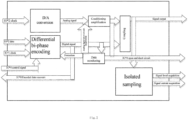
- the baseband signal generating device includes a D/A conversion unit, a differential bi-phase encoding unit, a conditioning and amplifying unit, a coupling unit, a re-collecting unit, a processing unit, a comparison unit, a control unit, a data monitoring unit, a display unit and an isolated sampling unit.
- an input terminal of the D/A conversion unit receives a first clock signal
- an output terminal of the D/A conversion unit communicates with an input terminal of the conditioning and amplifying unit
- an output terminal of the conditioning and amplifying unit communicates with an input terminal of the coupling unit.
- An input terminal of the differential bi-phase encoding unit receives a data signal and a second clock signal, and an output terminal of the differential bi-phase encoding unit communicates with the input terminal of the coupling unit.
- An output terminal of the coupling unit is configured to output a baseband signal.
- An input terminal of the data monitoring unit receives an output signal of the differential bi-phase encoding unit, and performs short-circuit protection on output signals of the differential bi-phase encoding unit and the D/A conversion unit, and an output terminal of the data monitoring unit sends monitoring information to the display unit.
- An input terminal of the re-collecting unit receives the output signal of differential bi-phase encoding unit, an output terminal of the re-collecting unit communicates with an input terminal of the processing unit, an output terminal of the processing unit communicates with an input terminal of the comparison unit, an output terminal of the comparison unit communicates with an input terminal of the control unit and the input terminal of the differential bi-phase encoding unit, and an output terminal of the control unit communicates with the input terminal of the differential bi-phase encoding unit.
- the isolated sampling unit communicates with the output terminal of the coupling unit, the isolated sampling unit includes a parallel step-down transformer and a series current transformer, the parallel step-down transformer performs voltage isolated sampling on a baseband signal output by the coupling unit, and the series current transformer performs current isolated sampling on the baseband signal output by the coupling unit.
- the baseband encoding device includes a disturbance unit, a data conversion unit, a scrambling unit, and a calculation unit; an input terminal of the disturbance unit receives the baseband signal, an output terminal of the disturbance unit communicates with an input terminal of the data conversion unit, an output terminal of the data conversion unit communicates with the input terminal of the scrambling unit, the output terminal of the scrambling unit communicates with an input terminal of the calculation unit, and an output terminal of the calculation unit is configured to output an encoded baseband signal.
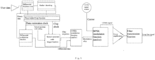
- the CDMA encoding device includes a decoding unit, a differential modulation unit, a spread-spectrum modulation unit, a carrier modulation unit, a signal amplification and filtering unit, and a phase-locked loop unit.
- the decoding unit includes a differential bi-phase decoding unit and a Barker decoding unit;
- a first input terminal of the differential bi-phase decoding unit receives the encoded baseband signal
- an output terminal of the differential bi-phase decoding unit communicates with a first input terminal of the Barker decoding unit
- an output terminal of the Barker decoding unit communicates with a first input terminal of the differential modulation unit
- an output terminal of the differential modulation unit communicates with a first input terminal of the CDMA modulation module
- a first input terminal of the spread-spectrum code trigger module is configured to set a spread-spectrum code
- an output terminal of the spread-spectrum code trigger module communicates with a second input terminal of the CDMA modulation module.
- An output terminal of the CDMA modulation module communicates with a first input terminal of the BPSK modulation module, an output terminal of a carrier signal communicates with a second input terminal of the BPSK modulation module, and an output terminal of the BPSK modulation module is connected to an input terminal of a power amplifier, an output terminal of the power amplifier is connected with an input terminal of the filter, and an output terminal of the filter outputs the CDMA encoded signal.
- An input terminal of the phase-locked loop unit receives the encoded baseband signal, and the phase-locked loop unit has a plurality of output terminals; a first output terminal of the phase-locked loop unit communicates with a second input terminal of the differential bi-phase decoding unit, a second output terminal communicates with a second input terminal of the Barker decoding unit, a third output terminal of the phase-locked loop unit communicates with a second output terminal of the differential modulation unit and a second output terminal of the spread-spectrum code trigger module, and a fourth output terminal of the phase-locked loop unit communicates with a third input terminal of the spread-spectrum code trigger module.
- S1 the baseband signal generating device receives a digital signal to generate a baseband signal, as shown in FIG. 1
- the D/A conversion unit receives the first clock signal, the first clock signal exemplarily comes from a Field Programmable Gate Array (FPGA) module, the FPGA module is preferably placed in a functional module with double 2-out-of-2 comparison and security self-checking, and the D/A conversion unit converts the first clock signal to obtain the analog signal, and outputs the analog signal;
- the figured show that there are two first clock signals, the D/A conversion unit receives the two first clock signals, the D/A conversion module generates analog signals from the two received first clock signals by a digital counter, and specifically, the digital counter uses one of the first clock signals as a data signal, and the other first clock signal as a counting clock, and the digital counter performs mixed accumulation at an output terminal, and then generates the analog signals through operation-amplification processing; and the analog signals are transmitted to the coupling unit after undergoing a series of conditioning processing of the operation and amplification and push-pull of the conditioning and amplifying unit.
- FPGA Field Programmable Gate Array
- the differential bi-phase encoding unit receives the data signal and the second clock signal, the data signal exemplarily comes from a CPU unit, the CPU unit is preferably placed in the functional module with double 2-out-of-2 comparison and security self-checking, the second clock signal comes from the FPGA module as well, the differential bi-phase encoding is performed on the data signal to obtain the encoded digital signal, and the encoded digital signal is output;
- the drawings show that the differential bi-phase encoding unit receives four data signals for differential bi-phase encoding, and specifically, a JK flip-flop is configured to carry out differential bi-phase hardware encoding on the four data signals by twice the frequency of the data rate to obtain encoded digital signals and the encoded digital signals are transmitted to the coupling unit.
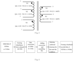
- the coupling unit receives an analog signal and an encoded digital signal, and performs coupling processing on the analog signal and the encoded digital signal to obtain a baseband signal, and specifically, two-in-one mixing and superposition are performed on the analog signal and the encoded digital signal by a synthetic transformer with a specific transformation ratio. Exemplarily, as shown in FIG.
- a first primary coil (input terminals 1 and 2) input analog signals
- a second primary coil (input terminals 3 and 5) input encoded digital signals
- a secondary coil outputs mixed and superimposed baseband signals
- the turns ratio of the first primary coil to the secondary coil is 35/92
- the turns ratio of the second primary coil to the secondary coil is 104/92 (that is, 26/23)
- the need of aliasing output of the signal amplitude of 14-18V and the signal amplitude of 20-23V is met, thereby generating a baseband signal complying with the European standard regulation, and exemplarily, bits of a baseband signal are 830 bits or 210 bits.
- an embodiment further uses the data monitoring unit to receive the encoded digital signal, and monitor the encoded digital signal, and the output of the analog signal and the encoded digital signal is cut off if a monitoring result shows that the encoded digital signal is a short-circuit signal, and specifically: the data monitoring unit monitors the encoded digital signal in manner of comparing the encoded digital signal with a preset threshold value, and if the encoded digital signal is greater than a preset threshold value, it indicates that the encoded digital signal is a short-circuit signal, at which time the data monitoring unit sends an alert message to the D/A conversion unit and the differential bi-phase encoding unit to facilitate the D/A conversion unit and the differential bi-phase encoding unit to cut off the output of the analog signal and the encoded digital signal, so as to implement the protection of the output signals of the differential bi-phase encoding unit and the D/A conversion unit, thereby guaranteeing security of an output signal of the coupling unit.
- the display unit receives the monitoring results of the data monitoring unit ( FIG. 2 shows that 8 monitoring results are received), and if a monitoring result shows that the encoded digital signal is a short-circuit signal, the display unit correspondingly displays a short-circuit state; and if a monitoring result shows that the encoded digital signal is an open-circuit signal, the display unit correspondingly displays an open-circuit state, and thus, it is convenient for an external staff to observe internal open and short-circuit states.
- an embodiment further uses the re-collecting unit to re-collect the encoded digital signal.
- the re-collecting unit re-collects 8 encoded digital signals
- the re-collecting unit transmits the 8 encoded digital signals to the processing unit
- the processing unit receives and decodes the re-collected encoded digital signals to obtain decoded digital signals
- the decoded digital signals are transmitted to the comparison unit
- the comparison unit compares the decoded digital signals with a data signal, if the decoded digital signals are consistent with the data signal, the encoded digital signals are output directly through the differential bi-phase encoding unit, and if the decoded digital signals are inconsistent with the data signal, the encoded digital signals are cut off under control of the control unit, and specifically, the control unit transmits four control signals to the differential bi-phase encoding unit, and the output of the encoded digital signals is cut off after the differential bi-phase encoding unit receives the control signals, further guaranteeing accuracy of the output signal of the
- an embodiment further uses the isolated sampling unit to perform isolated sampling of the baseband signal, and specifically, the isolated sampling unit is configured to perform voltage isolated sampling on the baseband signal of the coupling module through the parallel step-down transformer, and current isolated sampling through the series current transformer respectively, and abnormal output of baseband data is detected, thus guaranteeing effective output of data of the coupling unit.
- the disturbance unit receives the baseband signal (exemplary user data of 830bits or 210bits as shown in FIG. 4 ) and performs disturbance processing to obtain disturbed data and sends it to the data conversion unit; specifically, a 32-bit linear feedback shift register of a characteristic polynomial h (
- the data conversion unit receives the disturbed data and performs data conversion to obtain converted data, and sends it to the scrambling unit.
- the disturbed data is converted from 10bits to 11bits to obtain converted data of 913bits or 23 1bits; specifically, the disturbed data is grouped in the order of output by a codeword per 10bits, and then a pre-defined conversion table of 10bits to 11bits is used to perform data conversion on each codeword of 10bits from 10bits to 11bits.
- a conversion method is described as follows: a binary codeword of 10bits is represented by decimal x, then an x th 11bits data block is found out from the defined conversion table, and the 11bits data block is then a codeword of 11bits that is obtained after the conversion of the 10 bits codeword.
- the scrambling unit receives the converted data, and adds control bits and disturbance bits to the converted data to obtain scrambled data and sends it to the calculation unit.
- control bits are 3bits and the disturbance bits are 12bits.
- the calculation unit receives the scrambled data, selects additional trimming bits that meet the conditions, calculates check bits, and then adds the additional trimming bits and the check bits to the scrambled data to obtain an encoded baseband signal with specific bits, and exemplarily, the additional trimming bits are 10bits, the check bits are 85bits, and the bits of the encoded baseband signal are 1023bits or 341bits.
- S3 the CDMA encoding device performs CDMA encoding on the encoded baseband signal to obtain a CDMA encoded signal, as shown in FIG. 5 , which includes: S3-1: decoding the encoded baseband signal (that is, the user data in FIG. 5 ) to obtain the baseband decoded signal, specifically as follows:
- the first input terminal of the differential bi-phase decoding unit receives the encoded baseband signal, performs differential bi-phase decoding on the encoded baseband signal to obtain the initial decoded signal, and exemplarily, the differential bi-phase decoding unit performs Differential Bi-Phase Level (DBPL) decoding on the encoded baseband signal to obtain the initial decoded signal.
- DBPL Differential Bi-Phase Level
- the first input terminal of the Barker decoding unit receives the initial decoded signal, and performs Barker decoding on the initial decoded signal to obtain a baseband decoded signal (indicated as binary data in FIG. 5 ), and exemplarily, the Barker decoding unit converts the initial decoded signal into a Barker code 11100010010 of a 11-bit chip, then the Barker code 11100010010 of the 11-bit chip is demodulated to logic 1, and an inverse code of the Barker code of the 11-bit chip is demodulated to logic 0 to obtain a baseband decoded signal.
- modulation is performed on the baseband decoded signal, the modulation including differential modulation, spread-spectrum modulation and carrier modulation sequentially, and finally the carrier frequency signal is acquired, which is specifically described as follows:
- the first input terminal of the CDMA modulation module receives the differential modulated signal, and its second input terminal receives the address code, and direct sequence spread-spectrum modulation is performed on the differential modulation signal and the address code to obtain a spread-spectrum modulated signal (that is, a modulation chip in FIG. 5 ), and the spread-spectrum modulated signal is transmitted to the BPSK modulation module.
- a spread-spectrum modulated signal that is, a modulation chip in FIG. 5
- the carrier modulation unit performs carrier modulation on the spread-spectrum modulated signal to obtain a carrier frequency signal; specifically: The carrier signal source generates a carrier for carrier modulation, and the carrier is sent to the BPSK modulation module.
- the BPSK modulation module receives the carrier and the spread-spectrum modulated signal for carrier modulation, so that the spread-spectrum modulated signal is spread by N times to obtain a carrier frequency signal (that is, the CDMA signal in FIG. 5 ).
- the BPSK modulation module uses the carrier to spread the spread-spectrum modulated signal by 3 times to generate a carrier frequency signal of 13.545 MHz.
- the signal amplification and filtering unit performs amplification and filtering processing on the carrier frequency signal, specifically, The power amplifier performs amplification processing on the carrier frequency signal without power distortion, and then transmits an amplified signal to the filter, and the filter receives the amplified signal for filtering processing to guarantee the transmission quality of the carrier frequency signal, that is, the bit error rate is less than 10 -5 , undesired amplitude modulation is not greater than 7%, etc., and finally the CDMA encoded signal is obtained, that is, the CDMA encoded signal (that is, a loop line signal in FIG. 5 ) that conforms to the system of a signal that is received by the loop line transmission module of the European train operation control system.
- the CDMA encoded signal that is, a loop line signal in FIG. 5
- this embodiment further uses the phase-locked loop unit to guarantee the synchronization of encoded baseband signal processing, specifically, the input terminal of the phase-locked loop unit is configured to receive the encoded baseband signal.
- the first output terminal of the phase-locked loop unit outputs a signal to the second input terminal of the differential bi-phase decoding unit
- the second output terminal of the phase-locked loop unit outputs a signal to the second input terminal of the Barker decoding unit
- the third output terminal of the phase-locked loop unit outputs a signal to the second output terminal of the differential modulation unit and the second output terminal of the spread-spectrum code trigger module
- the fourth output terminal of the phase-locked loop unit outputs a signal to the third input terminal of the spread-spectrum code trigger module, thereby controlling the phase and frequency in the related signal processing processes of the differential bi-phase decoding unit, the Barker decoding unit, the differential modulation unit and the spread-spectrum code trigger module to kept synchronized with those of the input encoded baseband signal.
- this embodiment further provides a CDMA decoding system and decoding method.
- a decoded spread-spectrum code is transmitted to the loop line transmission module through an air interface in a signal system different from FSK through an European standard transponder of a signal device, and the loop line transmission module performs CDMA decoding with the decoded spread-spectrum code, and exemplarily, the European standard transponder used in this embodiment is a downsized European standard transponder that complies with ss-036.
- the CDMA decoding unit includes a Band-Pass Filter (BPF), an A/D module, a digital down-conversion module, a baseband signal interference processing module, and a demodulation module, the digital down-conversion module including a Low-Pass Filter (LPF) and a sampling module.
- BPF Band-Pass Filter
- A/D A/D
- digital down-conversion module a baseband signal interference processing module
- LPF Low-Pass Filter
- the CDMA decoding method specifically includes: Receiving the CDMA encoded signal (that is, r(t) in FIG. 6 ) by the band-pass filter, performing out-of-band noise and interference signal suppression on the CDMA encoded signal, and then transmitting the filtered signal to the A/D module.
- the A/D module realizes mid-band pass sampling, acquires the intermediate frequency digital signal and transmits it to the digital down-conversion module; wherein, the A/D module uses a 108.38 MHz crystal for sampling, with a bit width of 14bits, and the sampling rate is 8 times that of the CDMA carrier signal, which can adapt to signal scenarios with large DC offset and high dynamic range.
- the digital down-conversion module receives the intermediate frequency digital signal and down-converts the intermediate frequency signal to the baseband signal, that is, the carrier frequency of the intermediate frequency signal is removed to be restored into the CDMA encoded baseband signal.
- interference processing is performed on the intermediate frequency digital signal to reduce carrier synchronization and code capture errors.
- the interference processing of the intermediate frequency signal is realized in the digital down-conversion module, specifically the intermediate frequency digital signal is made to pass through the low-pass filter, and the low-pass filter has a flat passband characteristic and a group delay characteristic, so that a target signal can pass through the low-pass filter without distortion, and meanwhile, it has a very steep transition band, so that very good adjacent channel suppression capability can be provided.
- the typical adjacent channel suppression capability range of the low-pass filter is 30-90dB, and the intermediate frequency digital signal suppressed by the low-pass filter is sampled by the sampling module to be restored to the CDMA encoded baseband signal.
- this embodiment divides the intermediate frequency digital signal into two channels for interference processing, that is, the interference processing of the intermediate frequency signal is realized through a channel I and a channel Q respectively, so as to avoid that when one of the channels fails, the other channel can perform interference processing operation of the intermediate frequency signal normally.
- the baseband signal interference processing module eliminates possible adjacent channel interference and single-tone interference signals and the like of the European loop line from the CDMA encoded baseband signal to filter out a down-converted folding frequency component.
- the demodulation module restores the CDMA encoded baseband signal according to the known address spread-spectrum code number to obtain the CDMA decoded signal, and the drawings show use of a BPSK demodulation mode.
Landscapes
- Engineering & Computer Science (AREA)
- Computer Networks & Wireless Communication (AREA)
- Signal Processing (AREA)
- Digital Transmission Methods That Use Modulated Carrier Waves (AREA)
Description
- The present disclosure belongs to the technical field of railway communication, and particularly relates to a CDMA security encoding and decoding method and system.
- In order to adapt to rapid development of China's high-speed railways and passenger dedicated lines and to guarantee safety of railway transportation, China has successfully developed a China train control system, which is divided into application levels 0-4 according to functional requirements and configuration.
- With continuous development of Chinese railways in the European railway market, it is gradually noticed that train operation control systems of railways in Europe have a complex system, and various train control systems are not completely compatible, and therefore, it is necessary to develop a relevant signal transmission method and device that meet requirements for interconnection and intercommunication of a European railway operation control system.
- An existing European train operation control system has poor anti-interference performance, is only suitable for short distance transmission, has a high bit error rate and a high reception sensitivity threshold, is not capable of multipath reception, etc., due to use of signal systems such as Frequency Shift Keying (FSK), Phase Shift Keying (PSK) and the like.
-
US2003/161411 A1 discloses a bi-phase ultra wide band transmitter that communicates a bi-phase time-modulated UWB signal to a bi-phase time-modulated coherent receiver. The transmitter performs a source and channel encoding operation on the data in an encoder. The source encoding may be a differential encoding. Output of the encoder is provided to a digital encoder, which produces a length and digital code that encodes the data with a particular user code for an individual user or service. The length and code type may be typical codes such as those used in CDMA systems. The output of the digital encoder is provided to a bi-phase wavelet selector and analog encoder, which maps the respective outputs from the digital encoder into a particular analog encoded time-sequence of wavelets. The output of the selector and encoder is provided to preconditioning circuitry which can pass filters and cleans a signal prior to amplification and transmission. - In order to meet the needs of the prior art, the present disclosure provides a CDMA security encoding and decoding method and system, which can meet the requirements for interconnection and intercommunication of the European railway operation control system, and solves the problem that the existing European train operation control system has poor anti-interference performance, is only suitable for short-distance transmission, has a high bit error rate and high reception sensitivity threshold, is not capable of multi-path reception, etc., due to use of signal systems such as Frequency Shift Keying (FSK), Phase Shift Keying (PSK) and the like.
- The present disclosure is implemented through technical solutions defined in the appended claims.
- Compared with a closest prior art, the technical solution of the present disclosure has beneficial effects as follows:
- The present disclosure provides a CDMA security encoding method. Firstly, a digital signal is received to generate a baseband signal, then the baseband signal is encoded to obtain an encoded baseband signal, and then CDMA encoding is performed on the encoded baseband signal to obtain a CDMA encoded signal. The CDMA security encoding method is a new CDMA security encoding and decoding method that conforms to a loop line transmission module of the European train operation control system, which contributes to the interconnection and intercommunication of the European railway operation control system.
- The present disclosure provides a CDMA security encoding and decoding method, so that train-to-ground communication air interface transmission of a railway signal device of the European train operation control system uses a CDMA signal system, and compared with conventional signal systems, such as FSK, PSK and the like, the CDMA signal system has advantages of high anti-interference performance, extremely low bit error rate, longer transmission distance, extremely low reception sensitivity threshold, multi-path reception and the like.
- In order to explain the embodiments of the present disclosure or the technical solutions in the prior art more clearly, the drawings that need to be used in the description of the embodiments or the prior art will be briefly introduced below. Obviously, the drawings in the following description are only some embodiments of the present disclosure. For those of ordinary skill in the art, other drawings can be obtained based on these drawings without creative efforts.
-
FIG. 1 is an overall flow schematic diagram of a CDMA security encoding method of the present embodiments; -
FIG. 2 is a structural block diagram of generation of a baseband signal of the present embodiments; -
FIG. 3 is a structural block diagram of coupling processing of an analog signal and an encoded digital signal of the present embodiments; -
FIG. 4 shows a structure block diagram of baseband signal encoding; -
FIG. 5 is a structural block diagram of CDMA encoding of the present embodiments; and -
FIG. 6 is a structural block diagram of CDMA decoding of the present embodiments. - The technical solutions of the present disclosure will be clearly and completely described below in conjunction with the embodiments of the present disclosure. Obviously, the described embodiments are only a part of the embodiments of the present disclosure, rather than all the embodiments.
- A general CDMA technology is a mobile communication standard, which is mainly applied in a field of an industrial module for data transmission. It uses code sequence correlation to achieve multiple access communication, and a transmitted carrier is modulated by both a baseband digital signal and an address code. The division is implemented and identified according to different code pattern structures, and a pseudo-random code is generally selected as the address code. The general CDMA technology is a wireless spread-spectrum communication technology that appears in a digital mobile communication process, and it has characteristics of high spectrum utilization rate, high voice quality, high confidentiality, low call drop rate, low electromagnetic radiation, high capacity, wide coverage and the like.
- An embodiment provides a CDMA security encoding system, the CDMA security coding system including a baseband signal generating device, a baseband encoding device, and a CDMA encoding device.
- Wherein the baseband signal generating device includes a D/A conversion unit, a differential bi-phase encoding unit, a conditioning and amplifying unit, a coupling unit, a re-collecting unit, a processing unit, a comparison unit, a control unit, a data monitoring unit, a display unit and an isolated sampling unit.
- Wherein an input terminal of the D/A conversion unit receives a first clock signal, an output terminal of the D/A conversion unit communicates with an input terminal of the conditioning and amplifying unit, and an output terminal of the conditioning and amplifying unit communicates with an input terminal of the coupling unit.
- An input terminal of the differential bi-phase encoding unit receives a data signal and a second clock signal, and an output terminal of the differential bi-phase encoding unit communicates with the input terminal of the coupling unit.
- An output terminal of the coupling unit is configured to output a baseband signal.
- An input terminal of the data monitoring unit receives an output signal of the differential bi-phase encoding unit, and performs short-circuit protection on output signals of the differential bi-phase encoding unit and the D/A conversion unit, and an output terminal of the data monitoring unit sends monitoring information to the display unit.
- An input terminal of the re-collecting unit receives the output signal of differential bi-phase encoding unit, an output terminal of the re-collecting unit communicates with an input terminal of the processing unit, an output terminal of the processing unit communicates with an input terminal of the comparison unit, an output terminal of the comparison unit communicates with an input terminal of the control unit and the input terminal of the differential bi-phase encoding unit, and an output terminal of the control unit communicates with the input terminal of the differential bi-phase encoding unit.
- The isolated sampling unit communicates with the output terminal of the coupling unit, the isolated sampling unit includes a parallel step-down transformer and a series current transformer, the parallel step-down transformer performs voltage isolated sampling on a baseband signal output by the coupling unit, and the series current transformer performs current isolated sampling on the baseband signal output by the coupling unit.
- The baseband encoding device includes a disturbance unit, a data conversion unit, a scrambling unit, and a calculation unit; an input terminal of the disturbance unit receives the baseband signal, an output terminal of the disturbance unit communicates with an input terminal of the data conversion unit, an output terminal of the data conversion unit communicates with the input terminal of the scrambling unit, the output terminal of the scrambling unit communicates with an input terminal of the calculation unit, and an output terminal of the calculation unit is configured to output an encoded baseband signal.
- The CDMA encoding device includes a decoding unit, a differential modulation unit, a spread-spectrum modulation unit, a carrier modulation unit, a signal amplification and filtering unit, and a phase-locked loop unit.
- Wherein the decoding unit includes a differential bi-phase decoding unit and a Barker decoding unit;
- The spread-spectrum modulation unit includes a spread-spectrum code trigger module and a CDMA modulation module;
- The carrier modulation unit includes a carrier signal source and a BPSK modulation module; and
- The signal amplification and filtering unit includes a power amplifier and a filter.
- A first input terminal of the differential bi-phase decoding unit receives the encoded baseband signal, an output terminal of the differential bi-phase decoding unit communicates with a first input terminal of the Barker decoding unit, an output terminal of the Barker decoding unit communicates with a first input terminal of the differential modulation unit, an output terminal of the differential modulation unit communicates with a first input terminal of the CDMA modulation module, a first input terminal of the spread-spectrum code trigger module is configured to set a spread-spectrum code, and an output terminal of the spread-spectrum code trigger module communicates with a second input terminal of the CDMA modulation module.
- An output terminal of the CDMA modulation module communicates with a first input terminal of the BPSK modulation module, an output terminal of a carrier signal communicates with a second input terminal of the BPSK modulation module, and an output terminal of the BPSK modulation module is connected to an input terminal of a power amplifier, an output terminal of the power amplifier is connected with an input terminal of the filter, and an output terminal of the filter outputs the CDMA encoded signal.
- An input terminal of the phase-locked loop unit receives the encoded baseband signal, and the phase-locked loop unit has a plurality of output terminals; a first output terminal of the phase-locked loop unit communicates with a second input terminal of the differential bi-phase decoding unit, a second output terminal communicates with a second input terminal of the Barker decoding unit, a third output terminal of the phase-locked loop unit communicates with a second output terminal of the differential modulation unit and a second output terminal of the spread-spectrum code trigger module, and a fourth output terminal of the phase-locked loop unit communicates with a third input terminal of the spread-spectrum code trigger module.
- As shown in
FIG. 1 , there is provided a method for performing CDMA encoding using the CDMA security encoding system, which is specifically described as follows:
S1: the baseband signal generating device receives a digital signal to generate a baseband signal, as shown inFIG. 2 , specifically:
The D/A conversion unit receives the first clock signal, the first clock signal exemplarily comes from a Field Programmable Gate Array (FPGA) module, the FPGA module is preferably placed in a functional module with double 2-out-of-2 comparison and security self-checking, and the D/A conversion unit converts the first clock signal to obtain the analog signal, and outputs the analog signal; the figured show that there are two first clock signals, the D/A conversion unit receives the two first clock signals, the D/A conversion module generates analog signals from the two received first clock signals by a digital counter, and specifically, the digital counter uses one of the first clock signals as a data signal, and the other first clock signal as a counting clock, and the digital counter performs mixed accumulation at an output terminal, and then generates the analog signals through operation-amplification processing; and the analog signals are transmitted to the coupling unit after undergoing a series of conditioning processing of the operation and amplification and push-pull of the conditioning and amplifying unit. - The differential bi-phase encoding unit receives the data signal and the second clock signal, the data signal exemplarily comes from a CPU unit, the CPU unit is preferably placed in the functional module with double 2-out-of-2 comparison and security self-checking, the second clock signal comes from the FPGA module as well, the differential bi-phase encoding is performed on the data signal to obtain the encoded digital signal, and the encoded digital signal is output; the drawings show that the differential bi-phase encoding unit receives four data signals for differential bi-phase encoding, and specifically, a JK flip-flop is configured to carry out differential bi-phase hardware encoding on the four data signals by twice the frequency of the data rate to obtain encoded digital signals and the encoded digital signals are transmitted to the coupling unit.
- The coupling unit receives an analog signal and an encoded digital signal, and performs coupling processing on the analog signal and the encoded digital signal to obtain a baseband signal, and specifically, two-in-one mixing and superposition are performed on the analog signal and the encoded digital signal by a synthetic transformer with a specific transformation ratio. Exemplarily, as shown in
FIG. 3 , a first primary coil (input terminals 1 and 2) input analog signals, a second primary coil (input terminals 3 and 5) input encoded digital signals, and a secondary coil (output terminals 7 and 9) outputs mixed and superimposed baseband signals, wherein the turns ratio of the first primary coil to the secondary coil is 35/92, and the turns ratio of the second primary coil to the secondary coil is 104/92 (that is, 26/23), and then the need of aliasing output of the signal amplitude of 14-18V and the signal amplitude of 20-23V is met, thereby generating a baseband signal complying with the European standard regulation, and exemplarily, bits of a baseband signal are 830 bits or 210 bits. - As a preferred embodiment, an embodiment further uses the data monitoring unit to receive the encoded digital signal, and monitor the encoded digital signal, and the output of the analog signal and the encoded digital signal is cut off if a monitoring result shows that the encoded digital signal is a short-circuit signal, and specifically: the data monitoring unit monitors the encoded digital signal in manner of comparing the encoded digital signal with a preset threshold value, and if the encoded digital signal is greater than a preset threshold value, it indicates that the encoded digital signal is a short-circuit signal, at which time the data monitoring unit sends an alert message to the D/A conversion unit and the differential bi-phase encoding unit to facilitate the D/A conversion unit and the differential bi-phase encoding unit to cut off the output of the analog signal and the encoded digital signal, so as to implement the protection of the output signals of the differential bi-phase encoding unit and the D/A conversion unit, thereby guaranteeing security of an output signal of the coupling unit.
- Also, the display unit receives the monitoring results of the data monitoring unit (
FIG. 2 shows that 8 monitoring results are received), and if a monitoring result shows that the encoded digital signal is a short-circuit signal, the display unit correspondingly displays a short-circuit state; and if a monitoring result shows that the encoded digital signal is an open-circuit signal, the display unit correspondingly displays an open-circuit state, and thus, it is convenient for an external staff to observe internal open and short-circuit states. - Further, as a preferred embodiment, an embodiment further uses the re-collecting unit to re-collect the encoded digital signal. Specifically, the re-collecting unit re-collects 8 encoded digital signals, the re-collecting unit transmits the 8 encoded digital signals to the processing unit, the processing unit receives and decodes the re-collected encoded digital signals to obtain decoded digital signals, and the decoded digital signals are transmitted to the comparison unit, the comparison unit compares the decoded digital signals with a data signal, if the decoded digital signals are consistent with the data signal, the encoded digital signals are output directly through the differential bi-phase encoding unit, and if the decoded digital signals are inconsistent with the data signal, the encoded digital signals are cut off under control of the control unit, and specifically, the control unit transmits four control signals to the differential bi-phase encoding unit, and the output of the encoded digital signals is cut off after the differential bi-phase encoding unit receives the control signals, further guaranteeing accuracy of the output signal of the coupling unit.
- Further, as a preferred embodiment, an embodiment further uses the isolated sampling unit to perform isolated sampling of the baseband signal, and specifically, the isolated sampling unit is configured to perform voltage isolated sampling on the baseband signal of the coupling module through the parallel step-down transformer, and current isolated sampling through the series current transformer respectively, and abnormal output of baseband data is detected, thus guaranteeing effective output of data of the coupling unit.
- S2: the baseband encoding unit encodes the baseband signal to obtain an encoded baseband signal; specifically:
The disturbance unit receives the baseband signal (exemplary user data of 830bits or 210bits as shown inFIG. 4 ) and performs disturbance processing to obtain disturbed data and sends it to the data conversion unit; specifically, a 32-bit linear feedback shift register of a characteristic polynomial h (x) =x32+x31+x30+x29+x27+x25+...+1 is used to perform disturbance processing on the user data of 830bits or 210bits, where the initial value S of the characteristic polynomial is equal to (2801775573·B)mod232, and B is decimal representation of selected 12 disturbance bits. - The data conversion unit receives the disturbed data and performs data conversion to obtain converted data, and sends it to the scrambling unit. Exemplarily, the disturbed data is converted from 10bits to 11bits to obtain converted data of 913bits or 23 1bits; specifically, the disturbed data is grouped in the order of output by a codeword per 10bits, and then a pre-defined conversion table of 10bits to 11bits is used to perform data conversion on each codeword of 10bits from 10bits to 11bits. A conversion method is described as follows: a binary codeword of 10bits is represented by decimal x, then an xth 11bits data block is found out from the defined conversion table, and the 11bits data block is then a codeword of 11bits that is obtained after the conversion of the 10 bits codeword.
- The scrambling unit receives the converted data, and adds control bits and disturbance bits to the converted data to obtain scrambled data and sends it to the calculation unit. Exemplarily, the control bits are 3bits and the disturbance bits are 12bits.
- The calculation unit receives the scrambled data, selects additional trimming bits that meet the conditions, calculates check bits, and then adds the additional trimming bits and the check bits to the scrambled data to obtain an encoded baseband signal with specific bits, and exemplarily, the additional trimming bits are 10bits, the check bits are 85bits, and the bits of the encoded baseband signal are 1023bits or 341bits.
- S3: the CDMA encoding device performs CDMA encoding on the encoded baseband signal to obtain a CDMA encoded signal, as shown in
FIG. 5 , which includes:
S3-1: decoding the encoded baseband signal (that is, the user data inFIG. 5 ) to obtain the baseband decoded signal, specifically as follows:
The first input terminal of the differential bi-phase decoding unit receives the encoded baseband signal, performs differential bi-phase decoding on the encoded baseband signal to obtain the initial decoded signal, and exemplarily, the differential bi-phase decoding unit performs Differential Bi-Phase Level (DBPL) decoding on the encoded baseband signal to obtain the initial decoded signal. - The first input terminal of the Barker decoding unit receives the initial decoded signal, and performs Barker decoding on the initial decoded signal to obtain a baseband decoded signal (indicated as binary data in
FIG. 5 ), and exemplarily, the Barker decoding unit converts the initial decoded signal into a Barker code 11100010010 of a 11-bit chip, then the Barker code 11100010010 of the 11-bit chip is demodulated tologic 1, and an inverse code of the Barker code of the 11-bit chip is demodulated to logic 0 to obtain a baseband decoded signal. - S3-2: modulation is performed on the baseband decoded signal, the modulation including differential modulation, spread-spectrum modulation and carrier modulation sequentially, and finally the carrier frequency signal is acquired, which is specifically described as follows:
- S3-2-1: the first input terminal of the differential modulation unit receives the encoded baseband signal and performs differential modulation on the baseband decoded signal to obtain a differential modulated signal, and specifically, the differential modulation unit performs DBPL modulation on the baseband decoded signal to obtain the differential modulated signal (
FIG. 5 shows differential data) and sends it to the CDMA modulation module. - S3-2-2: the spread-spectrum modulation unit performs spread-spectrum modulation on the differential modulated signal to obtain a spread-spectrum modulated signal, specifically:
The spread-spectrum code trigger module is configured to generate an address code for CDMA spread-spectrum modulation, and then the address code (that is, a chip sequence inFIG. 5 ) is sent to the CDMA modulation module. Exemplarily, the bits of the address code are 472bits. - The first input terminal of the CDMA modulation module receives the differential modulated signal, and its second input terminal receives the address code, and direct sequence spread-spectrum modulation is performed on the differential modulation signal and the address code to obtain a spread-spectrum modulated signal (that is, a modulation chip in
FIG. 5 ), and the spread-spectrum modulated signal is transmitted to the BPSK modulation module. - S3-2-3: the carrier modulation unit performs carrier modulation on the spread-spectrum modulated signal to obtain a carrier frequency signal; specifically:
The carrier signal source generates a carrier for carrier modulation, and the carrier is sent to the BPSK modulation module. - The BPSK modulation module receives the carrier and the spread-spectrum modulated signal for carrier modulation, so that the spread-spectrum modulated signal is spread by N times to obtain a carrier frequency signal (that is, the CDMA signal in
FIG. 5 ). Preferably, the BPSK modulation module uses the carrier to spread the spread-spectrum modulated signal by 3 times to generate a carrier frequency signal of 13.545 MHz. - S3-3: the signal amplification and filtering unit performs amplification and filtering processing on the carrier frequency signal, specifically,
The power amplifier performs amplification processing on the carrier frequency signal without power distortion, and then transmits an amplified signal to the filter, and the filter receives the amplified signal for filtering processing to guarantee the transmission quality of the carrier frequency signal, that is, the bit error rate is less than 10-5, undesired amplitude modulation is not greater than 7%, etc., and finally the CDMA encoded signal is obtained, that is, the CDMA encoded signal (that is, a loop line signal inFIG. 5 ) that conforms to the system of a signal that is received by the loop line transmission module of the European train operation control system. - As a preferred embodiment, this embodiment further uses the phase-locked loop unit to guarantee the synchronization of encoded baseband signal processing, specifically, the input terminal of the phase-locked loop unit is configured to receive the encoded baseband signal.
- Then the first output terminal of the phase-locked loop unit outputs a signal to the second input terminal of the differential bi-phase decoding unit, the second output terminal of the phase-locked loop unit outputs a signal to the second input terminal of the Barker decoding unit, the third output terminal of the phase-locked loop unit outputs a signal to the second output terminal of the differential modulation unit and the second output terminal of the spread-spectrum code trigger module, and the fourth output terminal of the phase-locked loop unit outputs a signal to the third input terminal of the spread-spectrum code trigger module, thereby controlling the phase and frequency in the related signal processing processes of the differential bi-phase decoding unit, the Barker decoding unit, the differential modulation unit and the spread-spectrum code trigger module to kept synchronized with those of the input encoded baseband signal.
- Corresponding to the CDMA encoding method, this embodiment further provides a CDMA decoding system and decoding method. A decoded spread-spectrum code is transmitted to the loop line transmission module through an air interface in a signal system different from FSK through an European standard transponder of a signal device, and the loop line transmission module performs CDMA decoding with the decoded spread-spectrum code, and exemplarily, the European standard transponder used in this embodiment is a downsized European standard transponder that complies with ss-036.
- Specifically, as shown in
FIG. 6 , the CDMA decoding unit includes a Band-Pass Filter (BPF), an A/D module, a digital down-conversion module, a baseband signal interference processing module, and a demodulation module, the digital down-conversion module including a Low-Pass Filter (LPF) and a sampling module. - The CDMA decoding method specifically includes:
Receiving the CDMA encoded signal (that is, r(t) inFIG. 6 ) by the band-pass filter, performing out-of-band noise and interference signal suppression on the CDMA encoded signal, and then transmitting the filtered signal to the A/D module. - The A/D module realizes mid-band pass sampling, acquires the intermediate frequency digital signal and transmits it to the digital down-conversion module; wherein, the A/D module uses a 108.38 MHz crystal for sampling, with a bit width of 14bits, and the sampling rate is 8 times that of the CDMA carrier signal, which can adapt to signal scenarios with large DC offset and high dynamic range.
- The digital down-conversion module receives the intermediate frequency digital signal and down-converts the intermediate frequency signal to the baseband signal, that is, the carrier frequency of the intermediate frequency signal is removed to be restored into the CDMA encoded baseband signal. In order to better suppress a burst interference signal, interference processing is performed on the intermediate frequency digital signal to reduce carrier synchronization and code capture errors. The interference processing of the intermediate frequency signal is realized in the digital down-conversion module, specifically the intermediate frequency digital signal is made to pass through the low-pass filter, and the low-pass filter has a flat passband characteristic and a group delay characteristic, so that a target signal can pass through the low-pass filter without distortion, and meanwhile, it has a very steep transition band, so that very good adjacent channel suppression capability can be provided. The typical adjacent channel suppression capability range of the low-pass filter is 30-90dB, and the intermediate frequency digital signal suppressed by the low-pass filter is sampled by the sampling module to be restored to the CDMA encoded baseband signal.
- And as a backup shown in the drawings, this embodiment divides the intermediate frequency digital signal into two channels for interference processing, that is, the interference processing of the intermediate frequency signal is realized through a channel I and a channel Q respectively, so as to avoid that when one of the channels fails, the other channel can perform interference processing operation of the intermediate frequency signal normally. The baseband signal interference processing module eliminates possible adjacent channel interference and single-tone interference signals and the like of the European loop line from the CDMA encoded baseband signal to filter out a down-converted folding frequency component.
- The demodulation module restores the CDMA encoded baseband signal according to the known address spread-spectrum code number to obtain the CDMA decoded signal, and the drawings show use of a BPSK demodulation mode.
- The above embodiments are only used to illustrate rather than limit the technical solutions of the present disclosure. Although the present disclosure has been described in detail with reference to the above embodiments, its scope is defined only by the appended claims.
Claims (12)
- A CDMA security encoding method, comprising steps of:receiving a first clock signal, and converting the first clock signal into an analog signal;receiving a data signal and a second clock signal, and performing differential bi-phase encoding on the data signal to obtain an encoded digital signal;after conditioning and amplifying the analog signal, coupling the analog signal with the encoded digital signal, to obtain a desired baseband signal, wherein two-in-one mixing and superposition are is performed on the analog signal and the encoded digital signal by a synthetic transformer with a specific transformation ratio;encoding the baseband signal to obtain an encoded baseband signal, wherein a disturbance unit receives the baseband signal and performs disturbance processing to obtain disturbed data and sends it to a data conversion unit, the data conversion unit receives the disturbed data and performs data conversion to obtain converted data, and sends it to a scrambling unit, the scrambling unit receives the converted data, and adds control bits and disturbance bits to the converted data, so as to obtain scrambled data, and sends the scrambled data to a calculation unit; the calculation unit receives the scrambled data, selects additional trimming bits that meet specific conditions, calculates check bits, and then adds the additional trimming bits and the check bits to the scrambled data to obtain an encoded baseband signal with specific bits;
andperforming CDMA encoding on the encoded baseband signal to obtain an encoded CDMA signal. - The CDMA security encoding method according to claim 1, further comprising steps of:re-collecting the encoded digital signal;decoding the re-collected encoded digital signal to obtain a decoded digital signal;comparing the decoded digital signal with the data signal, and cutting off output of the encoded digital signal if the decoded digital signal is inconsistent with the data signal; andoutputting the encoded digital signal if the decoded digital signal is consistent with the data signal.
- The CDMA security encoding method according to claim 1, before receiving the analog signal and the encoded digital signal and performing coupling processing on the analog signal and the encoded digital signal, further comprising steps of:
receiving the encoded digital signal, monitoring the encoded digital signal, and cutting off the output of the analog signal and the encoded digital signal if a monitoring result shows that the encoded digital signal is a short-circuit signal. - The CDMA security encoding method according to claim 1, wherein the performing CDMA encoding on the encoded baseband signal to obtain a CDMA coded signal specifically comprises steps of:sequentially performing differential bi-phase decoding and Barker decoding on the encoded baseband signal to obtain a baseband decoded signal;performing differential modulation on the baseband decoded signal to obtain a differential modulated signal;generating an address code for spread-spectrum modulation, and performing direct sequence spread-spectrum modulation on the differential modulated signal and the address code to obtain a spread-spectrum modulated signal;generating a carrier for carrier modulation, and performing carrier modulation on the spread-spectrum modulated signal and the carrier, so that the spread-spectrum modulated signal is spread by N times, to obtain a carrier frequency signal; andperforming power amplification and filtering processing on the carrier frequency signal to obtain a CDMA encoded signal.
- The CDMA security encoding method according to claim 4, further comprising:receiving, by a phase-locked loop, the encoded baseband signal; andcontrolling, by the phase-locked loop, the frequency and phase in the processes of the differential bi-phase decoding, Barker decoding, differential modulation and address code generation according to the encoded baseband signal to be synchronized with those of the encoded baseband signal.
- A CDMA security encoding system, comprising a baseband signal generating device, a baseband encoding device and a CDMA encoding device; wherein the baseband signal generating device comprises a D/A conversion unit, a differential bi-phase encoding unit, a conditioning and amplifying unit and a coupling unit;the D/A conversion unit is configured to receive the first clock signal, and convert the first clock signal to obtain an analog signal;the differential bi-phase encoding unit is configured to receive the data signal and the second clock signal, and perform differential bi-phase encoding on the data signal to obtain an encoded digital signal;the conditioning and amplifying unit is configured to perform conditioning and amplifying on the analog signal to obtain a conditioned amplified analog signal;the coupling unit is configured to perform coupling processing on the conditioned and amplified analog signal and the encoded digital signal to obtain a desired baseband signal, wherein two-in-one mixing and superposition are performed on the analog signal and the encoded digital signal by a synthetic transformer with a specific transformation ratio;the baseband encoding device is configured to encode the baseband signal to obtain an encoded baseband signal, including a disturbance unit, a data conversion unit, a scrambling unit and a calculation unit, wherein the disturbance unit is configured to receive the baseband signal and performs disturbance processing to obtain disturbed data and send it to the data conversion unit, the data conversion unit is configured to receive the disturbed data and perform data conversion to obtain converted data, and send it to the scrambling unit, the scrambling unit is configured to receive the converted data, and add control bits and disturbance bits to the converted data, so as to obtain scrambled data, and send the scrambled data to the calculation unit; the calculation unit is configured to receive the scrambled data, select additional trimming bits that meet specific conditions, calculate check bits, and then add the additional trimming bits and the check bits to the scrambled data to obtain an encoded baseband signal with specific bits; andthe CDMA encoding device is configured to perform CDMA encoding on the baseband encoded signal to obtain a CDMA encoded signal.
- The CDMA security encoding system according to claim 6, wherein the baseband signal generating device further comprises a re-collecting unit, a processing unit, a comparison unit, and a control unit;the re-collecting unit is configured to re-collect an encoded digital signal;the processing unit is configured to decode the re-collected encoded digital signal to obtain a decoded digital signal;the comparison unit is configured to compare the decoded digital signal with the data signal, and the output of the encoded digital signal is cut off under control of the control unit if the decoded digital signal is inconsistent with the data signal; andthe encoded digital signal is output through the differential bi-phase encoding unit if the decoded digital signal is consistent with the data signal.
- The CDMA security encoding system according to claim 6, wherein the baseband signal generating device further comprises a data monitoring unit; and before the coupling unit performs coupling processing on the conditioned amplified analog signal and the encoded digital signal to obtain a baseband signal,
the data monitoring unit receives the encoded digital signal, and monitors the encoded digital signal, and output of the analog signal and the encoded digital signal is cut off if a monitoring result shows that the encoded digital signal is a short-circuit signal. - The CDMA security encoding system according to claim 6, wherein the CDMA encoding device comprises a differential bi-phase decoding unit, a Barker decoding unit, a differential modulation unit, a spread-spectrum modulation unit, a carrier modulation unit, and a signal amplification and filtering unit;the spread-spectrum modulation unit comprises a spread-spectrum code trigger module and a CDMA modulation module;the carrier modulation unit comprises a carrier signal source and a BPSK modulation module;the differential bi-phase decoding unit performs differential bi-phase decoding on the encoded baseband signal to obtain an initial decoded signal;the Barker decoding unit is configured to perform Barker decoding on the initial decoded signal to obtain a baseband decoded signal;the differential modulation unit is configured to perform differential modulation on the baseband decoded signal to obtain a differential modulated signal;the spread-spectrum code trigger module is configured to generate an address code for spread-spectrum modulation;the CDMA modulation module is configured to perform direct sequence spread-spectrum modulation on the differential modulated signal and the address code to obtain a spread-spectrum modulated signal;the carrier signal source is configured to generate a carrier for carrier modulation;the BPSK modulation module is configured to perform carrier modulation on the spread-spectrum modulated signal and the carrier, so that the spread-spectrum modulated signal is spread by N times, to obtain a carrier frequency signal; andthe signal amplification and filtering unit is configured to amplify and filter the carrier frequency signal to obtain a CDMA encoded signal.
- The CDMA security encoding system according to claim 9, wherein the CDMA encoding unit further comprises a phase-locked loop unit;
the phase-locked loop unit is configured to receive the encoded baseband signal, and control the frequency and phase in the processes of the differential bi-phase decoding, Barker decoding, differential modulation, and address code generation according to the encoded baseband signal to be synchronized with those of the encoded baseband signal. - CDMA security encoding and decoding method comprising the CDMA security encoding method of claim 1, comprising steps of:receiving, by a band-pass filter, the CDMA encoded signal, and performing filtering processing on the CDMA encoded signal to obtain a filtered signal;receiving, by an A/D module, the filtered signal, and performing mid-band pass sampling on the filtered signal to obtain an intermediate frequency digital signal;receiving, by a digital down-conversion module, the intermediate frequency digital signal, down-converting the intermediate frequency signal to a baseband signal, and performing interference processing on the intermediate frequency signal to obtain a CDMA encoded baseband signal;receiving, by a baseband signal interference processing module, the CDMA encoded baseband signal, and eliminating an adjacent channel and a single-tone interference signal in the CDMA encoded baseband signal to obtain a processed CDMA encoded baseband signal; andreceiving, by a demodulation module, the processed CDMA encoded baseband signal, and restoring the processed CDMA encoded baseband signal according to a known address spread-spectrum code number to obtain a CDMA decoded signal.
- CDMA security encoding and decoding system comprising the CDMA security encoding system of claim 6, further comprising a band-pass filter, an A/D module, a digital down-conversion module, a baseband signal interference processing module, and a demodulation module, and a digital down-conversion module; whereinthe band-pass filter is configured to receive the CDMA encoded signal, and suppress out-of-band noise and an interference signal in the CDMA encoded signal, to obtain a filtered signal;the A/D module is configured to receive the filtered signal, and perform mid-band pass sampling on the filtered signal to obtain an intermediate frequency digital signal;the digital down-conversion module is configured to receive the intermediate frequency digital signal, down-convert the intermediate frequency signal to a baseband signal, and perform interference processing on the intermediate frequency signal to obtain a CDMA encoded baseband signal;the baseband signal interference processing module is configured to receive the CDMA encoded baseband signal, and eliminate an adjacent channel and a single-tone interference signal to obtain a processed CDMA encoded baseband signal; andthe demodulation module is configured to receive the processed CDMA encoded baseband signal, and restore the processed CDMA encoded baseband signal according to the known address spread-spectrum code number to obtain a CDMA decoded signal.
Priority Applications (1)
| Application Number | Priority Date | Filing Date | Title |
|---|---|---|---|
| RS20241321A RS66224B1 (en) | 2021-06-17 | 2021-07-08 | Cdma secure encoding method and system, and cdma secure decoding method and system |
Applications Claiming Priority (2)
| Application Number | Priority Date | Filing Date | Title |
|---|---|---|---|
| CN202110668883.3A CN113131967B (en) | 2021-06-17 | 2021-06-17 | CDMA security coding and decoding method and system |
| PCT/CN2021/105123 WO2022262023A1 (en) | 2021-06-17 | 2021-07-08 | Cdma secure encoding method and system, and cdma secure decoding method and system |
Publications (4)
| Publication Number | Publication Date |
|---|---|
| EP4131789A1 EP4131789A1 (en) | 2023-02-08 |
| EP4131789A4 EP4131789A4 (en) | 2023-09-20 |
| EP4131789B1 true EP4131789B1 (en) | 2024-10-30 |
| EP4131789C0 EP4131789C0 (en) | 2024-10-30 |
Family
ID=76782992
Family Applications (1)
| Application Number | Title | Priority Date | Filing Date |
|---|---|---|---|
| EP21751949.5A Active EP4131789B1 (en) | 2021-06-17 | 2021-07-08 | Cdma secure encoding method and system, and cdma secure decoding method and system |
Country Status (5)
| Country | Link |
|---|---|
| EP (1) | EP4131789B1 (en) |
| CN (1) | CN113131967B (en) |
| HU (1) | HUE069504T2 (en) |
| RS (1) | RS66224B1 (en) |
| WO (1) | WO2022262023A1 (en) |
Families Citing this family (5)
| Publication number | Priority date | Publication date | Assignee | Title |
|---|---|---|---|---|
| CN114531178B (en) * | 2022-01-28 | 2023-03-21 | 珠海昇生微电子有限责任公司 | Charging and bidirectional communication system and method |
| CN115469897B (en) * | 2022-10-21 | 2025-12-02 | 无锡翼盟电子科技有限公司 | A printer consumable chip data update device based on Hall sensor |
| CN115454460B (en) * | 2022-10-21 | 2025-12-02 | 无锡翼盟电子科技有限公司 | A wireless update device for printer consumable chip data |
| CN117439618A (en) * | 2023-08-31 | 2024-01-23 | 广州市广源电子科技有限公司 | Railway FSK signal transmitting system based on GSMR network and high-reliability transmission method thereof |
| CN119030646A (en) * | 2024-10-17 | 2024-11-26 | 芯百特微电子(无锡)有限公司 | CDMA communication module test data analysis method based on data analysis |
Family Cites Families (12)
| Publication number | Priority date | Publication date | Assignee | Title |
|---|---|---|---|---|
| US5377226A (en) * | 1993-10-19 | 1994-12-27 | Hughes Aircraft Company | Fractionally-spaced equalizer for a DS-CDMA system |
| US6272121B1 (en) * | 1997-03-03 | 2001-08-07 | Omnipoint Corporation | Spread spectrum communication system using DECT protocol |
| US7280607B2 (en) * | 1997-12-12 | 2007-10-09 | Freescale Semiconductor, Inc. | Ultra wide bandwidth communications method and system |
| TWI234374B (en) * | 2003-03-04 | 2005-06-11 | Realtek Semiconductor Corp | Spread spectrum encoding method and spread spectrum encoding modulation method |
| US9217653B2 (en) * | 2007-09-13 | 2015-12-22 | Rosemount Inc. | High performance architecture for process transmitters |
| CN101505184B (en) * | 2009-02-27 | 2012-07-25 | 中国电子科技集团公司第五十四研究所 | Concealed satellite communication terminal |
| CN101969421B (en) * | 2010-09-19 | 2013-03-06 | 福建邮科通信技术有限公司 | Device for transmitting CDMA (Code Division Multiple Access) signal by adopting category V line |
| US9425854B2 (en) * | 2012-06-18 | 2016-08-23 | Alstom Transport Technologies | Spread spectrum signals in vehicle network systems |
| CN106157588B (en) * | 2016-08-15 | 2022-04-29 | 扬州恒隆软件有限公司 | Quick high-precision photoelectric direct-reading intelligent water meter system |
| CN108418603A (en) * | 2018-05-08 | 2018-08-17 | 北京凤凰汇通科技有限公司 | Terrestrial wireless spread spectrum communication system for railway |
| US10530618B1 (en) * | 2018-09-26 | 2020-01-07 | Qualcomm Incorporated | Single-ended to differential signal conversion of analog signals |
| CN110007325B (en) * | 2019-04-15 | 2022-09-13 | 中国电子科技集团公司第二十研究所 | Rapid frame synchronization method for satellite-based enhanced L5 signal |
-
2021
- 2021-06-17 CN CN202110668883.3A patent/CN113131967B/en active Active
- 2021-07-08 HU HUE21751949A patent/HUE069504T2/en unknown
- 2021-07-08 RS RS20241321A patent/RS66224B1/en unknown
- 2021-07-08 EP EP21751949.5A patent/EP4131789B1/en active Active
- 2021-07-08 WO PCT/CN2021/105123 patent/WO2022262023A1/en not_active Ceased
Also Published As
| Publication number | Publication date |
|---|---|
| RS66224B1 (en) | 2024-12-31 |
| WO2022262023A1 (en) | 2022-12-22 |
| EP4131789A1 (en) | 2023-02-08 |
| EP4131789A4 (en) | 2023-09-20 |
| CN113131967A (en) | 2021-07-16 |
| EP4131789C0 (en) | 2024-10-30 |
| HUE069504T2 (en) | 2025-03-28 |
| CN113131967B (en) | 2021-08-31 |
Similar Documents
| Publication | Publication Date | Title |
|---|---|---|
| EP4131789A1 (en) | Cdma secure encoding method and system, and cdma secure decoding method and system | |
| US5432815A (en) | Data modulator-demodulator apparatus of a spread spectrum communication system | |
| RU2266623C2 (en) | Method and device for transferring digital data at alternating speed | |
| EP2975814B1 (en) | Chirp Signal Processor | |
| US10270488B2 (en) | Binary high-power modulator | |
| EA031912B1 (en) | Combined amplitude-time modulation and phase modulation | |
| US20040146116A1 (en) | Apparatus for constant amplitude coded bi-orthogonal demodulation | |
| KR100528891B1 (en) | Method for producing a coded output signal and decoding method for producing a decoded datastream | |
| CN108988906B (en) | A non-coherent spread spectrum communication device with variable data rate | |
| CN110995334B (en) | Space-based frequency hopping data chain system with multi-channel parallel processing | |
| CN104661287A (en) | Multimode support parallel multichannel fast frequency sweeping method and multimode support parallel multichannel fast frequency sweeping system | |
| CN101946474A (en) | Pulse UWB Radio Communication System | |
| CN1883127B (en) | System and method for transmitting ultrawide bandwidth signals | |
| US11387864B2 (en) | Pulse based wideband signaling | |
| KR20090086104A (en) | Signaling scheme using transmitted reference pulses | |
| CN106130595A (en) | A marine ultra-short wave over-the-horizon communication device | |
| US9059790B2 (en) | Ultra-wide band communication apparatus and method | |
| US20050163235A1 (en) | Method and apparatus for improving error rates in multi-band ultra wideband communication systems | |
| EP1585229B1 (en) | Frequency staggered FSK | |
| CN101505184A (en) | Concealed satellite communication terminal | |
| CN110071739B (en) | Communication system and method based on frequency hopping, GMSK and DS | |
| CN111868545B (en) | A satellite communication navigation signal generating method and device, and receiving method and device | |
| AU2005251243A1 (en) | Integer cycle event detection using wavelet pass filter system and method | |
| CN108206701B (en) | Broadband radio frequency transmitting device, receiving device, transmitting method and receiving method | |
| CN116418365A (en) | A modulation and demodulation device based on in-band frequency hopping system |
Legal Events
| Date | Code | Title | Description |
|---|---|---|---|
| STAA | Information on the status of an ep patent application or granted ep patent |
Free format text: STATUS: UNKNOWN |
|
| STAA | Information on the status of an ep patent application or granted ep patent |
Free format text: STATUS: THE INTERNATIONAL PUBLICATION HAS BEEN MADE |
|
| PUAI | Public reference made under article 153(3) epc to a published international application that has entered the european phase |
Free format text: ORIGINAL CODE: 0009012 |
|
| STAA | Information on the status of an ep patent application or granted ep patent |
Free format text: STATUS: REQUEST FOR EXAMINATION WAS MADE |
|
| 17P | Request for examination filed |
Effective date: 20210818 |
|
| AK | Designated contracting states |
Kind code of ref document: A1 Designated state(s): AL AT BE BG CH CY CZ DE DK EE ES FI FR GB GR HR HU IE IS IT LI LT LU LV MC MK MT NL NO PL PT RO RS SE SI SK SM TR |
|
| RIN1 | Information on inventor provided before grant (corrected) |
Inventor name: XU, YANWEN Inventor name: CHEN, GUANG Inventor name: DING, HUAN Inventor name: ZHANG, SHENGWEN Inventor name: LV, XIANLIANG Inventor name: SUN, ZHENYU Inventor name: LI, XUEJIAN Inventor name: ZHANG, FUSONG Inventor name: SUN, GUOYING Inventor name: YE, FENG Inventor name: YANG, GUANGLUN Inventor name: WANG, GUOYING |
|
| A4 | Supplementary search report drawn up and despatched |
Effective date: 20230821 |
|
| RIC1 | Information provided on ipc code assigned before grant |
Ipc: H04B 1/40 20150101ALN20230814BHEP Ipc: H04K 1/02 20060101ALI20230814BHEP Ipc: H04B 1/3822 20150101ALI20230814BHEP Ipc: H04B 1/7097 20110101ALI20230814BHEP Ipc: H04B 1/7073 20110101ALI20230814BHEP Ipc: H04B 1/707 20110101AFI20230814BHEP |
|
| RIC1 | Information provided on ipc code assigned before grant |
Ipc: H04B 1/40 20150101ALN20240430BHEP Ipc: H04K 1/02 20060101ALI20240430BHEP Ipc: H04B 1/3822 20150101ALI20240430BHEP Ipc: H04B 1/7097 20110101ALI20240430BHEP Ipc: H04B 1/7073 20110101ALI20240430BHEP Ipc: H04B 1/707 20110101AFI20240430BHEP |
|
| GRAP | Despatch of communication of intention to grant a patent |
Free format text: ORIGINAL CODE: EPIDOSNIGR1 |
|
| STAA | Information on the status of an ep patent application or granted ep patent |
Free format text: STATUS: GRANT OF PATENT IS INTENDED |
|
| DAV | Request for validation of the european patent (deleted) | ||
| DAX | Request for extension of the european patent (deleted) | ||
| INTG | Intention to grant announced |
Effective date: 20240607 |
|
| GRAS | Grant fee paid |
Free format text: ORIGINAL CODE: EPIDOSNIGR3 |
|
| GRAA | (expected) grant |
Free format text: ORIGINAL CODE: 0009210 |
|
| STAA | Information on the status of an ep patent application or granted ep patent |
Free format text: STATUS: THE PATENT HAS BEEN GRANTED |
|
| AK | Designated contracting states |
Kind code of ref document: B1 Designated state(s): AL AT BE BG CH CY CZ DE DK EE ES FI FR GB GR HR HU IE IS IT LI LT LU LV MC MK MT NL NO PL PT RO RS SE SI SK SM TR |
|
| REG | Reference to a national code |
Ref country code: GB Ref legal event code: FG4D |
|
| REG | Reference to a national code |
Ref country code: CH Ref legal event code: EP |
|
| REG | Reference to a national code |
Ref country code: DE Ref legal event code: R096 Ref document number: 602021021051 Country of ref document: DE |
|
| REG | Reference to a national code |
Ref country code: IE Ref legal event code: FG4D |
|
| U01 | Request for unitary effect filed |
Effective date: 20241104 |
|
| U07 | Unitary effect registered |
Designated state(s): AT BE BG DE DK EE FI FR IT LT LU LV MT NL PT RO SE SI Effective date: 20241114 |
|
| REG | Reference to a national code |
Ref country code: SK Ref legal event code: T3 Ref document number: E 45393 Country of ref document: SK |
|
| REG | Reference to a national code |
Ref country code: HU Ref legal event code: AG4A Ref document number: E069504 Country of ref document: HU |
|
| PG25 | Lapsed in a contracting state [announced via postgrant information from national office to epo] |
Ref country code: IS Free format text: LAPSE BECAUSE OF FAILURE TO SUBMIT A TRANSLATION OF THE DESCRIPTION OR TO PAY THE FEE WITHIN THE PRESCRIBED TIME-LIMIT Effective date: 20250228 Ref country code: HR Free format text: LAPSE BECAUSE OF FAILURE TO SUBMIT A TRANSLATION OF THE DESCRIPTION OR TO PAY THE FEE WITHIN THE PRESCRIBED TIME-LIMIT Effective date: 20241030 |
|
| PG25 | Lapsed in a contracting state [announced via postgrant information from national office to epo] |
Ref country code: ES Free format text: LAPSE BECAUSE OF FAILURE TO SUBMIT A TRANSLATION OF THE DESCRIPTION OR TO PAY THE FEE WITHIN THE PRESCRIBED TIME-LIMIT Effective date: 20241030 |
|
| PG25 | Lapsed in a contracting state [announced via postgrant information from national office to epo] |
Ref country code: NO Free format text: LAPSE BECAUSE OF FAILURE TO SUBMIT A TRANSLATION OF THE DESCRIPTION OR TO PAY THE FEE WITHIN THE PRESCRIBED TIME-LIMIT Effective date: 20250130 |
|
| PG25 | Lapsed in a contracting state [announced via postgrant information from national office to epo] |
Ref country code: GR Free format text: LAPSE BECAUSE OF FAILURE TO SUBMIT A TRANSLATION OF THE DESCRIPTION OR TO PAY THE FEE WITHIN THE PRESCRIBED TIME-LIMIT Effective date: 20250131 |
|
| PG25 | Lapsed in a contracting state [announced via postgrant information from national office to epo] |
Ref country code: PL Free format text: LAPSE BECAUSE OF FAILURE TO SUBMIT A TRANSLATION OF THE DESCRIPTION OR TO PAY THE FEE WITHIN THE PRESCRIBED TIME-LIMIT Effective date: 20241030 |
|
| PG25 | Lapsed in a contracting state [announced via postgrant information from national office to epo] |
Ref country code: SM Free format text: LAPSE BECAUSE OF FAILURE TO SUBMIT A TRANSLATION OF THE DESCRIPTION OR TO PAY THE FEE WITHIN THE PRESCRIBED TIME-LIMIT Effective date: 20241030 |
|
| PGFP | Annual fee paid to national office [announced via postgrant information from national office to epo] |
Ref country code: RS Payment date: 20250613 Year of fee payment: 5 |
|
| U20 | Renewal fee for the european patent with unitary effect paid |
Year of fee payment: 5 Effective date: 20250606 |
|
| PGFP | Annual fee paid to national office [announced via postgrant information from national office to epo] |
Ref country code: SK Payment date: 20250523 Year of fee payment: 5 |
|
| PG25 | Lapsed in a contracting state [announced via postgrant information from national office to epo] |
Ref country code: CZ Free format text: LAPSE BECAUSE OF FAILURE TO SUBMIT A TRANSLATION OF THE DESCRIPTION OR TO PAY THE FEE WITHIN THE PRESCRIBED TIME-LIMIT Effective date: 20241030 |
|
| PLBE | No opposition filed within time limit |
Free format text: ORIGINAL CODE: 0009261 |
|
| STAA | Information on the status of an ep patent application or granted ep patent |
Free format text: STATUS: NO OPPOSITION FILED WITHIN TIME LIMIT |
|
| PGFP | Annual fee paid to national office [announced via postgrant information from national office to epo] |
Ref country code: HU Payment date: 20250610 Year of fee payment: 5 |
|
| 26N | No opposition filed |
Effective date: 20250731 |
|
| PGFP | Annual fee paid to national office [announced via postgrant information from national office to epo] |
Ref country code: CH Payment date: 20250801 Year of fee payment: 5 |
|
| GBPC | Gb: european patent ceased through non-payment of renewal fee |
Effective date: 20250708 |
|
| PG25 | Lapsed in a contracting state [announced via postgrant information from national office to epo] |
Ref country code: GB Free format text: LAPSE BECAUSE OF NON-PAYMENT OF DUE FEES Effective date: 20250708 |
|
| U1N | Appointed representative for the unitary patent procedure changed after the registration of the unitary effect |
Representative=s name: MARKS & CLERK LLP; GB |