EP4131364A2 - Integrated circuit chip including a passivation nitride layer in contact with a high voltage bonding pad and method of making - Google Patents
Integrated circuit chip including a passivation nitride layer in contact with a high voltage bonding pad and method of making Download PDFInfo
- Publication number
- EP4131364A2 EP4131364A2 EP22188099.0A EP22188099A EP4131364A2 EP 4131364 A2 EP4131364 A2 EP 4131364A2 EP 22188099 A EP22188099 A EP 22188099A EP 4131364 A2 EP4131364 A2 EP 4131364A2
- Authority
- EP
- European Patent Office
- Prior art keywords
- layer
- nitride layer
- passivation
- integrated circuit
- opening
- Prior art date
- Legal status (The legal status is an assumption and is not a legal conclusion. Google has not performed a legal analysis and makes no representation as to the accuracy of the status listed.)
- Withdrawn
Links
Images




Classifications
-
- H—ELECTRICITY
- H10—SEMICONDUCTOR DEVICES; ELECTRIC SOLID-STATE DEVICES NOT OTHERWISE PROVIDED FOR
- H10W—GENERIC PACKAGES, INTERCONNECTIONS, CONNECTORS OR OTHER CONSTRUCTIONAL DETAILS OF DEVICES COVERED BY CLASS H10
- H10W74/00—Encapsulations, e.g. protective coatings
- H10W74/01—Manufacture or treatment
-
- H—ELECTRICITY
- H10—SEMICONDUCTOR DEVICES; ELECTRIC SOLID-STATE DEVICES NOT OTHERWISE PROVIDED FOR
- H10W—GENERIC PACKAGES, INTERCONNECTIONS, CONNECTORS OR OTHER CONSTRUCTIONAL DETAILS OF DEVICES COVERED BY CLASS H10
- H10W74/00—Encapsulations, e.g. protective coatings
- H10W74/10—Encapsulations, e.g. protective coatings characterised by their shape or disposition
- H10W74/131—Encapsulations, e.g. protective coatings characterised by their shape or disposition the semiconductor body being only partially enclosed
- H10W74/147—Encapsulations, e.g. protective coatings characterised by their shape or disposition the semiconductor body being only partially enclosed the encapsulations being multilayered
-
- H—ELECTRICITY
- H10—SEMICONDUCTOR DEVICES; ELECTRIC SOLID-STATE DEVICES NOT OTHERWISE PROVIDED FOR
- H10W—GENERIC PACKAGES, INTERCONNECTIONS, CONNECTORS OR OTHER CONSTRUCTIONAL DETAILS OF DEVICES COVERED BY CLASS H10
- H10W20/00—Interconnections in chips, wafers or substrates
- H10W20/40—Interconnections external to wafers or substrates, e.g. back-end-of-line [BEOL] metallisations or vias connecting to gate electrodes
- H10W20/45—Interconnections external to wafers or substrates, e.g. back-end-of-line [BEOL] metallisations or vias connecting to gate electrodes characterised by their insulating parts
- H10W20/47—Interconnections external to wafers or substrates, e.g. back-end-of-line [BEOL] metallisations or vias connecting to gate electrodes characterised by their insulating parts comprising two or more dielectric layers having different properties, e.g. different dielectric constants
-
- H—ELECTRICITY
- H10—SEMICONDUCTOR DEVICES; ELECTRIC SOLID-STATE DEVICES NOT OTHERWISE PROVIDED FOR
- H10W—GENERIC PACKAGES, INTERCONNECTIONS, CONNECTORS OR OTHER CONSTRUCTIONAL DETAILS OF DEVICES COVERED BY CLASS H10
- H10W20/00—Interconnections in chips, wafers or substrates
- H10W20/40—Interconnections external to wafers or substrates, e.g. back-end-of-line [BEOL] metallisations or vias connecting to gate electrodes
- H10W20/495—Capacitive arrangements or effects of, or between wiring layers
- H10W20/496—Capacitor integral with wiring layers
-
- H—ELECTRICITY
- H10—SEMICONDUCTOR DEVICES; ELECTRIC SOLID-STATE DEVICES NOT OTHERWISE PROVIDED FOR
- H10W—GENERIC PACKAGES, INTERCONNECTIONS, CONNECTORS OR OTHER CONSTRUCTIONAL DETAILS OF DEVICES COVERED BY CLASS H10
- H10W20/00—Interconnections in chips, wafers or substrates
- H10W20/40—Interconnections external to wafers or substrates, e.g. back-end-of-line [BEOL] metallisations or vias connecting to gate electrodes
- H10W20/497—Inductive arrangements or effects of, or between, wiring layers
-
- H—ELECTRICITY
- H10—SEMICONDUCTOR DEVICES; ELECTRIC SOLID-STATE DEVICES NOT OTHERWISE PROVIDED FOR
- H10W—GENERIC PACKAGES, INTERCONNECTIONS, CONNECTORS OR OTHER CONSTRUCTIONAL DETAILS OF DEVICES COVERED BY CLASS H10
- H10W72/00—Interconnections or connectors in packages
- H10W72/01—Manufacture or treatment
- H10W72/019—Manufacture or treatment of bond pads
-
- H—ELECTRICITY
- H10—SEMICONDUCTOR DEVICES; ELECTRIC SOLID-STATE DEVICES NOT OTHERWISE PROVIDED FOR
- H10W—GENERIC PACKAGES, INTERCONNECTIONS, CONNECTORS OR OTHER CONSTRUCTIONAL DETAILS OF DEVICES COVERED BY CLASS H10
- H10W72/00—Interconnections or connectors in packages
- H10W72/01—Manufacture or treatment
- H10W72/019—Manufacture or treatment of bond pads
- H10W72/01908—Manufacture or treatment of bond pads using permanent auxiliary members, e.g. using alignment marks
-
- H—ELECTRICITY
- H10—SEMICONDUCTOR DEVICES; ELECTRIC SOLID-STATE DEVICES NOT OTHERWISE PROVIDED FOR
- H10W—GENERIC PACKAGES, INTERCONNECTIONS, CONNECTORS OR OTHER CONSTRUCTIONAL DETAILS OF DEVICES COVERED BY CLASS H10
- H10W72/00—Interconnections or connectors in packages
- H10W72/20—Bump connectors, e.g. solder bumps or copper pillars; Dummy bumps; Thermal bumps
-
- H—ELECTRICITY
- H10—SEMICONDUCTOR DEVICES; ELECTRIC SOLID-STATE DEVICES NOT OTHERWISE PROVIDED FOR
- H10W—GENERIC PACKAGES, INTERCONNECTIONS, CONNECTORS OR OTHER CONSTRUCTIONAL DETAILS OF DEVICES COVERED BY CLASS H10
- H10W72/00—Interconnections or connectors in packages
- H10W72/20—Bump connectors, e.g. solder bumps or copper pillars; Dummy bumps; Thermal bumps
- H10W72/29—Bond pads specially adapted therefor
-
- H—ELECTRICITY
- H10—SEMICONDUCTOR DEVICES; ELECTRIC SOLID-STATE DEVICES NOT OTHERWISE PROVIDED FOR
- H10W—GENERIC PACKAGES, INTERCONNECTIONS, CONNECTORS OR OTHER CONSTRUCTIONAL DETAILS OF DEVICES COVERED BY CLASS H10
- H10W72/00—Interconnections or connectors in packages
- H10W72/50—Bond wires
-
- H—ELECTRICITY
- H10—SEMICONDUCTOR DEVICES; ELECTRIC SOLID-STATE DEVICES NOT OTHERWISE PROVIDED FOR
- H10W—GENERIC PACKAGES, INTERCONNECTIONS, CONNECTORS OR OTHER CONSTRUCTIONAL DETAILS OF DEVICES COVERED BY CLASS H10
- H10W72/00—Interconnections or connectors in packages
- H10W72/50—Bond wires
- H10W72/59—Bond pads specially adapted therefor
-
- H—ELECTRICITY
- H10—SEMICONDUCTOR DEVICES; ELECTRIC SOLID-STATE DEVICES NOT OTHERWISE PROVIDED FOR
- H10W—GENERIC PACKAGES, INTERCONNECTIONS, CONNECTORS OR OTHER CONSTRUCTIONAL DETAILS OF DEVICES COVERED BY CLASS H10
- H10W72/00—Interconnections or connectors in packages
- H10W72/90—Bond pads, in general
-
- H—ELECTRICITY
- H10—SEMICONDUCTOR DEVICES; ELECTRIC SOLID-STATE DEVICES NOT OTHERWISE PROVIDED FOR
- H10W—GENERIC PACKAGES, INTERCONNECTIONS, CONNECTORS OR OTHER CONSTRUCTIONAL DETAILS OF DEVICES COVERED BY CLASS H10
- H10W72/00—Interconnections or connectors in packages
- H10W72/90—Bond pads, in general
- H10W72/921—Structures or relative sizes of bond pads
- H10W72/923—Bond pads having multiple stacked layers
-
- H—ELECTRICITY
- H10—SEMICONDUCTOR DEVICES; ELECTRIC SOLID-STATE DEVICES NOT OTHERWISE PROVIDED FOR
- H10W—GENERIC PACKAGES, INTERCONNECTIONS, CONNECTORS OR OTHER CONSTRUCTIONAL DETAILS OF DEVICES COVERED BY CLASS H10
- H10W72/00—Interconnections or connectors in packages
- H10W72/90—Bond pads, in general
- H10W72/941—Dispositions of bond pads
- H10W72/9415—Dispositions of bond pads relative to the surface, e.g. recessed, protruding
-
- H—ELECTRICITY
- H10—SEMICONDUCTOR DEVICES; ELECTRIC SOLID-STATE DEVICES NOT OTHERWISE PROVIDED FOR
- H10W—GENERIC PACKAGES, INTERCONNECTIONS, CONNECTORS OR OTHER CONSTRUCTIONAL DETAILS OF DEVICES COVERED BY CLASS H10
- H10W72/00—Interconnections or connectors in packages
- H10W72/90—Bond pads, in general
- H10W72/941—Dispositions of bond pads
- H10W72/942—Dispositions of bond pads relative to underlying supporting features, e.g. bond pads, RDLs or vias
-
- H—ELECTRICITY
- H10—SEMICONDUCTOR DEVICES; ELECTRIC SOLID-STATE DEVICES NOT OTHERWISE PROVIDED FOR
- H10W—GENERIC PACKAGES, INTERCONNECTIONS, CONNECTORS OR OTHER CONSTRUCTIONAL DETAILS OF DEVICES COVERED BY CLASS H10
- H10W72/00—Interconnections or connectors in packages
- H10W72/90—Bond pads, in general
- H10W72/951—Materials of bond pads
- H10W72/952—Materials of bond pads comprising metals or metalloids, e.g. PbSn, Ag or Cu
-
- H—ELECTRICITY
- H10—SEMICONDUCTOR DEVICES; ELECTRIC SOLID-STATE DEVICES NOT OTHERWISE PROVIDED FOR
- H10W—GENERIC PACKAGES, INTERCONNECTIONS, CONNECTORS OR OTHER CONSTRUCTIONAL DETAILS OF DEVICES COVERED BY CLASS H10
- H10W72/00—Interconnections or connectors in packages
- H10W72/90—Bond pads, in general
- H10W72/981—Auxiliary members, e.g. spacers
Definitions
- the present invention relates to an integrated circuit chip and, in particular, to an architecture for a high voltage bonding pad that utilizes a passivation nitride layer in contact with the pad and self-aligned to a photosensitive insulator.
- an integrated circuit chip it is known in the art for an integrated circuit chip to include a high voltage integrated passive component, such as an inductor or capacitor, in the metallization layers which extend over the semiconductor substrate where the active integrated circuit components, such as transistors, are fabricated.
- a high voltage integrated passive component such as an inductor or capacitor
- a terminal of this passive component may be electrically connected to a high voltage metal bonding pad of the integrated circuit chip.
- the current state of the art for making this physical connection is to utilize a construction in the back end of line (BEOL) processing referred to in the art as Nickel-Palladium finishing.
- BEOL back end of line
- Nickel-Palladium finishing is not always available in the technology platform.
- the alternative known to those skilled in the art is to utilize a dedicated processing mask in the back end finishing process in order to make the connection between the passivation nitride layer and the metal bonding pad. This solution adds an extra cost to the integrated circuit fabrication.
- FIG. 1 shows a cross-section of an integrated circuit chip 10 including a front end of line (FEOL) structure and a back end of line (BEOL) structure.
- the front end of line (FEOL) structure includes, for example, a semiconductor substrate, active integrated circuits (transistors, diodes, etc.), metal contacts, and a pre-metallization dielectric (PMD) layer, as known to those skilled in the art.
- the BEOL structure is formed over the FEOL structure and includes an interconnect comprising a plurality of metallization layers 12, with the layers 12 including metal structures such as connection lines and vias supported in an insulating material.
- the metal structures of the layers are formed by Copper and the insulating material is Silicon oxide.
- the integrated circuit chip 10 further includes a high voltage passive circuit component 14 formed in one or more of the plurality of metallization layers.
- Figure 1 shows a transformer for the passive circuit component 14 which is formed by metal structures on two separate layers 12 to provide a pair of spiral wound inductors 16a, 16b.
- the passive circuit component 14 could comprise a capacitor.
- the metal structures in the upper-most (or top) layer 12t of the BEOL structure further include a metal pad 20.
- the metal pad 20 is electrically coupled (preferably directly connected) by a connection line in the upper-most layer 12t to a terminal of the high voltage passive circuit component 14 (for example, to an end of the spiral wound inductor 16b).
- a top surface of the metal pad 20 and top surface of the insulating material of the upper-most layer 12t present a coplanar top surface 22 of the interconnect.
- a metal cap finishing structure 32 (e.g., a bonding pad and/or a redistribution layer (RDL)) is provided within the opening and in contact with the top surface of the metal pad 20. This metal cap finishing structure 32 further extends outside the opening on an upper surface of the stack of insulating layers.
- the metal cap finishing structure 32 is made of Aluminum.
- a passivation structure extends conformally over the plurality of metallization layers 12, the stack of insulating layers and the metal cap finishing structure 32.
- This passivation structure comprises at least one insulating layer 38.
- the insulating layer 38 is made of Silicon oxide.
- An opening in the passivation structure provided by the insulating layer 38 exposes a portion of the top surface 52 of the metal cap finishing structure 32.
- a nitride layer 42 extends conformally over the passivation insulating layer 38. Because of the presence of the opening in the passivation insulating layer 38, the nitride layer 42 extends on a sidewall 46 of the layer 38 at the opening and further extends on (and in contact with) the top surface of the metal-cap finishing structure 32.
- the portion of nitride layer 42 extending on the top surface of the metal cap finishing structure 32 is referred to as the foot 48 of the nitride layer, and it is this connection of the nitride layer 42 at the foot 48 to the high voltage bonding pad (metal cap finishing structure 32) that presents the significant reliability advantage noted above.
- the insulator region 50 is provided over the Nitride layer 42.
- the insulator region 50 is, e.g., of photosensitive material; for example, a carbon-based polymer that is used as a protection layer for the integrated circuit.
- This polymer may comprise a photoresist that may be lithographically defined and temperature cured to a stable physical and chemical configuration.
- the lithographic definition may form an opening which exposes a top surface of the Nitride layer 42.
- This opening is further used as a mask opening to define through an etching process the physical extent of the foot 48 self-aligned with the insulator region 50.
- etching, nitride layer 42 includes an opening which exposes the upper surface of the metal cap finishing structure 32.
- a ball bond or wire bond 56 may then be made to the metal cap finishing structure 32 at this exposed upper surface.
- Figure 2 illustrates the structure following completion of a standard process flow in the BEOL process up to the point where definition of the metal cap finishing structure 32 has been completed.
- a lithographic patterning using tools and processes well known in the art is performed to form an opening that exposes to the top surface of a portion of the metal pad 20 in the upper-most metallization layer 12t.
- the Aluminum material for the metal cap finishing structure 32 is then conformally (blanket) deposited in a layer which fills the opening and extends over the top surface of the stack.
- a lithographic patterning process is then performed to remove unwanted portions of the Aluminum material layer and define the size and extent of the metal cap finishing structure 32.
- a conformal (blanket) deposition of a passivation oxide material layer 38 is made.
- the material used for layer 38 may, for example, be a Silicon oxide. The result is shown in Figure 3 .
- the passivation oxide layer 38 is then lithographically patterned to form an opening 39 exposing a portion 37 of the top surface of the metal cap finishing structure 32 and define a passivation structure.
- the result is shown in Figure 4 .
- the nitride layer 42 is conformally (blanket) deposited over the passivation insulating layer 38.
- the nitride layer 42 extends along the sidewall 46 of the opening 39 and further covers (contacts) the exposed portion 37 of the top surface of the metal cap finishing structure 32.
- the material used for nitride layer 42 may, for example, be a Silicon nitride.
- An insulator material e.g., a photoresist
- a spin-coating process can be used to produce a layer 49 of the insulator material (insulator material layer 49). See Figure 6 .
- the insulator material may, for example, be a carbon-based polymer resist.
- the insulator material layer 49 is then lithographically defined and temperature cured. As a result, the insulator material layer 49 forms the insulator region 50 with a mask opening 51. The result is shown in Figure 7 .
- etching is then performed using the insulator region 50 as a mask.
- the etching removes a portion of the nitride layer 42 located in the mask opening 51 to expose the top surface of the metal cap finishing structure 32.
- This etching through the nitride layer 42 further defines the extent of the foot 48 of the Nitride layer 42 so that it is self-aligned to the opening in the insulator region 50 while remaining in contact with the top surface of the metal cap finishing structure 32.
- the result is shown in Figure 8 .
- the advantage presented by the fabrication process as described above is that no additional dedicated mask for patterning the Nitride layer 42 (and foot 48) is needed. Rather, the fabrication process takes advantage of the masking used in connection with defining the opening in the insulator region 50 to self-align the foot 48 of the Nitride layer 42.
- FIG. 9 shows a cross-section of an alternative embodiment of the integrated circuit chip 10.
- the chip 10 of Figure 9 differs from the chip 10 of Figure 1 in that the passivation structure includes a passivation nitride layer 40 in addition to the oxide layer 38. The opening in the passivation structure accordingly extends through both passivation layers (nitride and oxide).
- Figures 10 to 16 show steps in the back end of line (BEOL) process to make the structure shown in Figure 9 .
- Figure 10 corresponds to Figure 2 and for the sake of brevity will not be described again.
- the stack includes a passivation oxide material layer 38 and a passivation nitride layer 40.
- the material used for layer 38 may, for example, be a Silicon oxide
- the material used for passivation nitride layer 40 may, for example, be a Silicon nitride.
- the result is shown in Figure 11 .
- the stack of passivation layers is then lithographically patterned to form an opening 39 exposing a portion 37 of the top surface of the metal cap finishing structure 32 and define a passivation structure.
- the result is shown in Figure 12 .
- a further nitride layer 42 is conformally (blanket) deposited over the passivation structure (patterned insulating layers 38 and 40).
- the nitride layer 42 extends along the sidewall 46 of the opening 39 and further covers (contacts) the exposed portion 37 of the top surface of the metal cap finishing structure 32.
- the material used for nitride layer 42 may, for example, be a Silicon nitride.
- An insulator material is coated on the nitride layer 42.
- a spin-coating process can be used to produce an insulator layer 49, e.g., of a photosensitive insulator material, in the form of a photoresist. See, Figure 14 .
- the photosensitive insulator material may, for example, be a carbon-based polymer resist.
- the insulator layer 49 is then lithographically defined and temperature cured. As a result, the layer 49 forms insulator region 50 with a mask opening 51. The result is shown in Figure 15 .
- etching is then performed using the insulator region 50 as a mask.
- the etching removes a portion of the nitride layer 42 in the mask opening 51 to expose the top surface of the metal cap finishing structure 32.
- This etching through the nitride layer 42 further defines the extent of the foot 48 of the Nitride layer 42 so that it is self-aligned to the opening in the insulator region 50 while remaining in contact with the top surface of the metal cap finishing structure 32.
- the result is shown in Figure 16 .
- the Nitride layer 42 with foot 48 self-aligned to the insulator region 50 can be used in connection with any last metal structure 100 of the integrated circuit chip 10 (for example, as shown, located in the upper-most layer 12t of the interconnect).
- the last metal structure 100 may comprise a Copper and/or Aluminum pad in layer 12t with supporting vias 102 in the underlying layer 12.
- the passivation oxide layer 38 (with or without passivation nitride layer 40) covers the peripheral region of the last metal structure 100 and the insulating material of the layer 12t.
- the conformally (blanket) deposited Nitride layer 42 is then patterned using the opening in the insulator region 50 to access the top surface of the last metal structure 100.
- the BEOL process shown in Figures 3-8 may be used to make the structures as shown in Figure 17 . Additionally, it will be recognized that the passivation structure could instead comprise both passivation oxide layer 38 and passivation nitride layer 40, as shown in Figure 18 , in which case the BEOL process shown in Figures 11-16 may be used to make the structures.
- An integrated circuit chip may be summarized as comprising:
- the passivation structure may comprise an oxide layer.
- the passivation structure may comprise an oxide layer and a nitride layer.
- the last metal structure may comprise an Aluminum pad.
- the last metal structure may comprises a Copper pad.
- the last metal structure may comprise:
- the integrated circuit chip may further comprise a stack of insulating layers on a top surface of the upper-most metallization layer, wherein a third opening extends through the stack of insulating layers to expose a portion of the upper surface of the metal pad, and wherein said metal cap finishing structure further extends on an upper surface of the stack of insulating layers.
- the stack of insulating layers may comprise:
- the integrated circuit chip may further comprise a passive circuit component having a terminal electrically connected to the last metal structure.
- the passive circuit component is formed in one or more metallization layers of the BEOL structure.
- the passive circuit component may be one of an inductor or a capacitor.
- a method of making may be summarize as comprising:
- the passivation layer may comprises an oxide layer.
- the passivation layer may comprise a stack of an oxide layer and a nitride layer.
- the last metal structure may comprise an Aluminum pad.
- the method may further comprise:
- the stack of insulating layers may comprise:
- the method may further comprise forming the last metal structure within a back end of line (BEOL) structure of an integrated circuit.
- BEOL back end of line
- the method may further comprise forming the last metal structure within an upper-most metallization layer of an integrated circuit.
- the method may further comprise:
- the passive circuit component may be formed in one or more metallization layers of the BEOL structure.
- the passive circuit component may be one of an inductor or a capacitor.
Landscapes
- Internal Circuitry In Semiconductor Integrated Circuit Devices (AREA)
- Engineering & Computer Science (AREA)
- Manufacturing & Machinery (AREA)
- Wire Bonding (AREA)
Abstract
Description
- The present invention relates to an integrated circuit chip and, in particular, to an architecture for a high voltage bonding pad that utilizes a passivation nitride layer in contact with the pad and self-aligned to a photosensitive insulator.
- It is known in the art for an integrated circuit chip to include a high voltage integrated passive component, such as an inductor or capacitor, in the metallization layers which extend over the semiconductor substrate where the active integrated circuit components, such as transistors, are fabricated.
- A terminal of this passive component may be electrically connected to a high voltage metal bonding pad of the integrated circuit chip.
- Those skilled in the art recognize that there is a significant reliability advantage if the passivation nitride layer is placed in contact with (i.e., physically connected to) the high voltage metal bonding pad.
- The current state of the art for making this physical connection is to utilize a construction in the back end of line (BEOL) processing referred to in the art as Nickel-Palladium finishing. However, Nickel-Palladium finishing is not always available in the technology platform. When Nickel-Palladium finishing is not available, the alternative known to those skilled in the art is to utilize a dedicated processing mask in the back end finishing process in order to make the connection between the passivation nitride layer and the metal bonding pad. This solution adds an extra cost to the integrated circuit fabrication.
- There is accordingly a need in the art for a BEOL process that supports the making of a physical connection between the passivation nitride layer and the high voltage metal bonding pad without requiring either specialized Nickel-Palladium finishing or a dedicated processing mask.
- Accordingly, an integrated circuit chip and a method of making are provided, as defined in the accompanying claims.
- For an understanding of the invention, reference will now be made by way of example only to the accompanying figures in which:
-
Figure 1 shows a cross section of an integrated circuit chip; -
Figures 2 to 8 show steps in the back end of line (BEOL) process to make the structure shown inFigure 1 ; -
Figure 9 shows a cross section of an alternative embodiment of an integrated circuit chip; -
Figures 10 to 16 show steps in the BEOL process to make the structure shown inFigure 9 ; and -
Figures 17 and 18 show cross sections of further alternative embodiments of an integrated circuit chip. - Reference is made to
Figure 1 which shows a cross-section of an integratedcircuit chip 10 including a front end of line (FEOL) structure and a back end of line (BEOL) structure. The front end of line (FEOL) structure includes, for example, a semiconductor substrate, active integrated circuits (transistors, diodes, etc.), metal contacts, and a pre-metallization dielectric (PMD) layer, as known to those skilled in the art. The BEOL structure is formed over the FEOL structure and includes an interconnect comprising a plurality ofmetallization layers 12, with thelayers 12 including metal structures such as connection lines and vias supported in an insulating material. For example, the metal structures of the layers are formed by Copper and the insulating material is Silicon oxide. - The
integrated circuit chip 10 further includes a high voltagepassive circuit component 14 formed in one or more of the plurality of metallization layers. As an example,Figure 1 shows a transformer for thepassive circuit component 14 which is formed by metal structures on twoseparate layers 12 to provide a pair ofspiral wound inductors passive circuit component 14 could comprise a capacitor. The metal structures in the upper-most (or top)layer 12t of the BEOL structure further include ametal pad 20. Although not explicitly shown, themetal pad 20 is electrically coupled (preferably directly connected) by a connection line in theupper-most layer 12t to a terminal of the high voltage passive circuit component 14 (for example, to an end of thespiral wound inductor 16b). - A top surface of the
metal pad 20 and top surface of the insulating material of theupper-most layer 12t present a coplanartop surface 22 of the interconnect. A stack of insulating layers, comprising aSilicon nitride layer 26 andSilicon oxide layer 28, for example, rests on thatcoplanar surface 22. - An opening in the stack of
insulating layers metal pad 20. A metal cap finishing structure 32 (e.g., a bonding pad and/or a redistribution layer (RDL)) is provided within the opening and in contact with the top surface of themetal pad 20. This metalcap finishing structure 32 further extends outside the opening on an upper surface of the stack of insulating layers. For example, the metalcap finishing structure 32 is made of Aluminum. - A passivation structure extends conformally over the plurality of
metallization layers 12, the stack of insulating layers and the metalcap finishing structure 32. This passivation structure comprises at least oneinsulating layer 38. For example, theinsulating layer 38 is made of Silicon oxide. An opening in the passivation structure provided by theinsulating layer 38 exposes a portion of thetop surface 52 of the metalcap finishing structure 32. - A
nitride layer 42 extends conformally over thepassivation insulating layer 38. Because of the presence of the opening in thepassivation insulating layer 38, thenitride layer 42 extends on asidewall 46 of thelayer 38 at the opening and further extends on (and in contact with) the top surface of the metal-cap finishing structure 32. The portion ofnitride layer 42 extending on the top surface of the metalcap finishing structure 32 is referred to as thefoot 48 of the nitride layer, and it is this connection of thenitride layer 42 at thefoot 48 to the high voltage bonding pad (metal cap finishing structure 32) that presents the significant reliability advantage noted above. - An
insulator region 50 is provided over the Nitridelayer 42. Theinsulator region 50 is, e.g., of photosensitive material; for example, a carbon-based polymer that is used as a protection layer for the integrated circuit. - This polymer may comprise a photoresist that may be lithographically defined and temperature cured to a stable physical and chemical configuration. The lithographic definition may form an opening which exposes a top surface of the Nitride
layer 42. - This opening is further used as a mask opening to define through an etching process the physical extent of the
foot 48 self-aligned with theinsulator region 50. As a result of that, etching,nitride layer 42 includes an opening which exposes the upper surface of the metalcap finishing structure 32. A ball bond orwire bond 56 may then be made to the metalcap finishing structure 32 at this exposed upper surface. - Reference is now made to
Figures 2 to 8 which show steps in the back end of line (BEOL) process to make the structure shown inFigure 1 . -
Figure 2 illustrates the structure following completion of a standard process flow in the BEOL process up to the point where definition of the metalcap finishing structure 32 has been completed. As part of this standard process flow, after deposition of the stack of insulating layers (Silicon nitride layer 26 and Silicon oxide layer 28) on thecoplanar surface 22, a lithographic patterning using tools and processes well known in the art is performed to form an opening that exposes to the top surface of a portion of themetal pad 20 in theupper-most metallization layer 12t. The Aluminum material for the metalcap finishing structure 32 is then conformally (blanket) deposited in a layer which fills the opening and extends over the top surface of the stack. A lithographic patterning process is then performed to remove unwanted portions of the Aluminum material layer and define the size and extent of the metalcap finishing structure 32. - Next, a conformal (blanket) deposition of a passivation
oxide material layer 38 is made. The material used forlayer 38 may, for example, be a Silicon oxide. The result is shown inFigure 3 . - The
passivation oxide layer 38 is then lithographically patterned to form anopening 39 exposing aportion 37 of the top surface of the metalcap finishing structure 32 and define a passivation structure. The result is shown inFigure 4 . - In
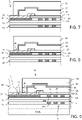
Figure 5 , thenitride layer 42 is conformally (blanket) deposited over thepassivation insulating layer 38. Thenitride layer 42 extends along thesidewall 46 of theopening 39 and further covers (contacts) the exposedportion 37 of the top surface of the metalcap finishing structure 32. The material used fornitride layer 42 may, for example, be a Silicon nitride. - An insulator material, e.g., a photoresist, is coated on the
nitride layer 42. For example, a spin-coating process can be used to produce alayer 49 of the insulator material (insulator material layer 49). SeeFigure 6 . The insulator material may, for example, be a carbon-based polymer resist. - The
insulator material layer 49 is then lithographically defined and temperature cured. As a result, theinsulator material layer 49 forms theinsulator region 50 with a mask opening 51. The result is shown inFigure 7 . - An etching is then performed using the
insulator region 50 as a mask. The etching removes a portion of thenitride layer 42 located in themask opening 51 to expose the top surface of the metalcap finishing structure 32. This etching through thenitride layer 42 further defines the extent of thefoot 48 of theNitride layer 42 so that it is self-aligned to the opening in theinsulator region 50 while remaining in contact with the top surface of the metalcap finishing structure 32. The result is shown inFigure 8 . - The advantage presented by the fabrication process as described above is that no additional dedicated mask for patterning the Nitride layer 42 (and foot 48) is needed. Rather, the fabrication process takes advantage of the masking used in connection with defining the opening in the
insulator region 50 to self-align thefoot 48 of theNitride layer 42. - Reference is made to
Figure 9 which shows a cross-section of an alternative embodiment of theintegrated circuit chip 10. Like references inFigures 1 and9 refer to like or similar components. Thechip 10 ofFigure 9 differs from thechip 10 ofFigure 1 in that the passivation structure includes apassivation nitride layer 40 in addition to theoxide layer 38. The opening in the passivation structure accordingly extends through both passivation layers (nitride and oxide). -
Figures 10 to 16 show steps in the back end of line (BEOL) process to make the structure shown inFigure 9 . -
Figure 10 corresponds toFigure 2 and for the sake of brevity will not be described again. - Next, a conformal (blanket) deposition of a stack of passivation layers is made. The stack includes a passivation
oxide material layer 38 and apassivation nitride layer 40. The material used forlayer 38 may, for example, be a Silicon oxide, and the material used forpassivation nitride layer 40 may, for example, be a Silicon nitride. The result is shown inFigure 11 . - The stack of passivation layers is then lithographically patterned to form an
opening 39 exposing aportion 37 of the top surface of the metalcap finishing structure 32 and define a passivation structure. The result is shown inFigure 12 . - In
Figure 13 , afurther nitride layer 42 is conformally (blanket) deposited over the passivation structure (patterned insulatinglayers 38 and 40). Thenitride layer 42 extends along thesidewall 46 of theopening 39 and further covers (contacts) the exposedportion 37 of the top surface of the metalcap finishing structure 32. The material used fornitride layer 42 may, for example, be a Silicon nitride. - An insulator material is coated on the
nitride layer 42. For example, a spin-coating process can be used to produce aninsulator layer 49, e.g., of a photosensitive insulator material, in the form of a photoresist. See,Figure 14 . The photosensitive insulator material may, for example, be a carbon-based polymer resist. - The
insulator layer 49 is then lithographically defined and temperature cured. As a result, thelayer 49 forms insulatorregion 50 with amask opening 51. The result is shown inFigure 15 . - An etching is then performed using the
insulator region 50 as a mask. The etching removes a portion of thenitride layer 42 in themask opening 51 to expose the top surface of the metalcap finishing structure 32. This etching through thenitride layer 42 further defines the extent of thefoot 48 of theNitride layer 42 so that it is self-aligned to the opening in theinsulator region 50 while remaining in contact with the top surface of the metalcap finishing structure 32. The result is shown inFigure 16 . - Reference is made to
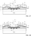
Figures 17 and 18 which show cross-sections of alternative embodiments of theintegrated circuit chip 10. Like references inFigures 1 ,9 and17-18 refer to like or similar components. TheNitride layer 42 withfoot 48 self-aligned to theinsulator region 50 can be used in connection with anylast metal structure 100 of the integrated circuit chip 10 (for example, as shown, located in theupper-most layer 12t of the interconnect). In this embodiment, thelast metal structure 100 may comprise a Copper and/or Aluminum pad inlayer 12t with supportingvias 102 in theunderlying layer 12. The passivation oxide layer 38 (with or without passivation nitride layer 40) covers the peripheral region of thelast metal structure 100 and the insulating material of thelayer 12t. The conformally (blanket) depositedNitride layer 42 is then patterned using the opening in theinsulator region 50 to access the top surface of thelast metal structure 100. - The BEOL process shown in
Figures 3-8 may be used to make the structures as shown inFigure 17 . Additionally, it will be recognized that the passivation structure could instead comprise bothpassivation oxide layer 38 andpassivation nitride layer 40, as shown inFigure 18 , in which case the BEOL process shown inFigures 11-16 may be used to make the structures. - The foregoing description has provided by way of exemplary and non-limiting examples of a full and informative description of the exemplary embodiment of this invention. However, various modifications and adaptations may become apparent to those skilled in the relevant arts in view of the foregoing description, when read in conjunction with the accompanying drawings and the appended claims. However, all such and similar modifications of the teachings of this invention will still fall within the scope of this invention as defined in the appended claims.
- An integrated circuit chip may be summarized as comprising:
- a front end of line (FEOL) structure;
- a back end of line (BEOL) structure over the FEOL structure;
- wherein the BEOL structure includes:
- a last metal structure providing a bonding pad;
- a passivation structure covering a peripheral region of the last metal structure and including a first opening extending through the passivation structure and exposing an upper surface of the last metal structure;
- a conformal nitride layer extending over the passivation structure and in contact with the upper surface of the last metal structure; and
- an
insulator material layer 49 covering the conformal nitride layer and including a second opening extending through both the insulator material layer and the conformal nitride layer, where a foot portion of the conformal nitride layer on the upper surface of the last metal structure is self-aligned with the second opening.
- The passivation structure may comprise an oxide layer.
- The passivation structure may comprise an oxide layer and a nitride layer.
- The last metal structure may comprise an Aluminum pad.
- The last metal structure may comprises a Copper pad.
- The last metal structure may comprise:
- a metal pad at an upper-most metallization layer of the BEOL structure; and
- a metal cap finishing structure in contact with an upper surface of the metal pad.
- The metal pad may be made of Copper and the metal cap finishing structure may be made of Aluminum.
- The integrated circuit chip may further comprise a stack of insulating layers on a top surface of the upper-most metallization layer, wherein a third opening extends through the stack of insulating layers to expose a portion of the upper surface of the metal pad, and wherein said metal cap finishing structure further extends on an upper surface of the stack of insulating layers.
- The stack of insulating layers may comprise:
- a nitride layer on the top surface of the upper-most metallization layer; and
- an oxide layer on top of the nitride layer.
- The integrated circuit chip may further comprise a passive circuit component having a terminal electrically connected to the last metal structure.
- The passive circuit component is formed in one or more metallization layers of the BEOL structure.
- The passive circuit component may be one of an inductor or a capacitor.
- A method of making may be summarize as comprising:
- depositing a passivation layer over a last metal structure providing a bonding pad;
- forming a first opening extending through the passivation layer to define a passivation structure and expose an upper surface of the last metal structure;
- conformally depositing a nitride layer extending over the passivation structure and in contact with the upper surface of the last metal structure;
- coating the nitride layer with an insulator material layer;
- forming a second opening extending through the insulator material layer; and
- using the insulator material layer with the second opening as a mask to etch through the nitride layer and expose the upper surface of the last metal structure, where a foot portion of the nitride layer on the upper surface of the last metal structure is self-aligned with the second opening.
- In the method ,the passivation layer may comprises an oxide layer.
- In the method, the passivation layer may comprise a stack of an oxide layer and a nitride layer.
- In the method, the last metal structure may comprise an Aluminum pad.
- in the method, the last metal structure may comprise a Copper pad.
- in the method , the last metal structure may comprise:
- a metal pad at an upper-most metallization layer of a BEOL structure; and a metal cap finishing structure in contact with an upper surface of the metal pad.
- The method may further comprise:
- depositing a stack of insulating layers extending over the upper-most metallization layer;
- forming a third opening extending through the stack of insulating layers to expose a portion of the upper surface of the metal pad; and
- forming said metal cap finishing structure to extend over an upper surface of the stack of insulating layers.
- In the method, the stack of insulating layers may comprise:
- a nitride layer on the top surface of the upper-most metallization layer; and
- an oxide layer on top of the nitride layer.
- The method may further comprise forming the last metal structure within a back end of line (BEOL) structure of an integrated circuit.
- The method may further comprise forming the last metal structure within an upper-most metallization layer of an integrated circuit.
- The method may further comprise:
- forming a passive circuit component within a back end of line (BEOL) structure of an integrated circuit; and
- electrically connecting a terminal of the passive circuit component to the last metal structure.
- In the method, the passive circuit component may be formed in one or more metallization layers of the BEOL structure.
- In the method, the passive circuit component may be one of an inductor or a capacitor.
Claims (15)
- An integrated circuit chip, comprising:a front end of line (FEOL) structure;a back end of line (BEOL) structure over the FEOL structure;wherein the BEOL structure includes:a last metal structure (20, 32: 100) providing a bonding pad (20);a passivation structure (38; 40) covering a peripheral region of the last metal structure and including a first opening (39) extending through the passivation structure and exposing an upper surface of the last metal structure;a conformal nitride layer (42) extending over the passivation structure and in contact with the upper surface of the last metal structure; andan insulator region (50) covering the conformal nitride layer (42) and including a second opening (51) extending through both the insulator region (50) and the conformal nitride layer (42), where a foot portion of the conformal nitride layer on the upper surface of the last metal structure is self-aligned with the second opening.
- The integrated circuit chip of claim 1, wherein the passivation structure (38; 40) comprises an oxide layer (38).
- The integrated circuit chip of claim 1, wherein the passivation structure (38; 40) comprises an oxide layer (38) and a nitride layer (40).
- The integrated circuit chip of any of the preceding claims, wherein the last metal structure comprises an Aluminum or Copper pad (32).
- The integrated circuit chip of claim 1, wherein the bonding pad (20) is formed in the upper-most metallization layer of the BEOL structure and the last metal structure (32: 100) further comprises:
a metal cap finishing structure (32) in contact with an upper surface of the bonding pad (20). - The integrated circuit chip of the preceding claim, wherein the metal pad (20) is made of Copper and the metal cap finishing structure (32) is made of Aluminum.
- The integrated circuit chip of claim 5 or 6, further comprising a stack of insulating layers (26, 28) on a top surface of the upper-most metallization layer (12t), wherein a third opening extends through the stack of insulating layers to expose a portion of the upper surface of the metal pad (20), and wherein said metal cap finishing structure(32) further extends on an upper surface of the stack of insulating layers.
- The integrated circuit chip of the preceding claim, wherein the stack of insulating layers comprises:a nitride layer (26) on the top surface of the upper-most metallization layer (12t); andan oxide layer (28) on top of the nitride layer.
- A method of making an integrated circuit chip, comprising:depositing a passivation layer (38, 40) over a last metal structure (20, 32: 100) providing a bonding pad (20);forming a first opening extending through the passivation layer to define a passivation structure and expose an upper surface (52) of the last metal structure;conformally depositing a nitride layer (42) extending over the passivation structure (38, 40) and in contact with the upper surface of the last metal structure;coating the nitride layer (42) with an insulator material layer (49);forming a second opening (51) extending through the insulator material layer (49); andusing the insulator material layer with the second opening as a mask to etch through the nitride layer (42) and expose the upper surface of the last metal structure, where a foot portion (48) of the nitride layer (42) on the upper surface of the last metal structure is self-aligned with the second opening.
- The method of the preceding claim, wherein the passivation layer (38; 40) comprises an oxide layer (38) and/or a nitride layer (40).
- The method of claim 9 or 10, wherein the last metal structure (20, 32: 100) comprises an Aluminum or a Copper pad.
- The method of any of claims 9-11, wherein the bonding pad is formed in the upper-most metallization layer of the BEOL structure and the last metal structure further comprises:
a metal cap finishing structure (32) in contact with an upper surface of the bonding pad (20). - The method of any of claim 9-12, further comprising:depositing a stack of insulating layers (26, 28) extending over the upper-most metallization layer (12t);forming a third opening extending through the stack of insulating layers to expose a portion of the upper surface of the bonding pad (20); andforming said metal cap finishing structure (32) to extend over an upper surface of the stack of insulating layers.
- The method of the previous claim, wherein the stack of insulating layers comprises:a nitride layer (26) on the top surface of the upper-most metallization layer (12t); andan oxide layer (28) on top of the nitride layer.
- The method of any of claims 9-14, further comprising forming the last metal structure (32) within a back end of line (BEOL) structure of an integrated circuit.
Applications Claiming Priority (1)
| Application Number | Priority Date | Filing Date | Title |
|---|---|---|---|
| US17/391,192 US11887948B2 (en) | 2021-08-02 | 2021-08-02 | Integrated circuit chip including a passivation nitride layer in contact with a high voltage bonding pad and method of making |
Publications (2)
| Publication Number | Publication Date |
|---|---|
| EP4131364A2 true EP4131364A2 (en) | 2023-02-08 |
| EP4131364A3 EP4131364A3 (en) | 2023-06-14 |
Family
ID=82786857
Family Applications (1)
| Application Number | Title | Priority Date | Filing Date |
|---|---|---|---|
| EP22188099.0A Withdrawn EP4131364A3 (en) | 2021-08-02 | 2022-08-01 | Integrated circuit chip including a passivation nitride layer in contact with a high voltage bonding pad and method of making |
Country Status (3)
| Country | Link |
|---|---|
| US (2) | US11887948B2 (en) |
| EP (1) | EP4131364A3 (en) |
| CN (2) | CN218498062U (en) |
Families Citing this family (1)
| Publication number | Priority date | Publication date | Assignee | Title |
|---|---|---|---|---|
| US11887948B2 (en) * | 2021-08-02 | 2024-01-30 | Stmicroelectronics S.R.L. | Integrated circuit chip including a passivation nitride layer in contact with a high voltage bonding pad and method of making |
Family Cites Families (15)
| Publication number | Priority date | Publication date | Assignee | Title |
|---|---|---|---|---|
| US6709965B1 (en) * | 2002-10-02 | 2004-03-23 | Taiwan Semiconductor Manufacturing Company | Aluminum-copper bond pad design and method of fabrication |
| US7863742B2 (en) | 2007-11-01 | 2011-01-04 | Taiwan Semiconductor Manufacturing Company, Ltd. | Back end integrated WLCSP structure without aluminum pads |
| JP5775321B2 (en) * | 2011-02-17 | 2015-09-09 | トランスフォーム・ジャパン株式会社 | Semiconductor device, manufacturing method thereof, and power supply device |
| US9245833B2 (en) | 2012-08-30 | 2016-01-26 | Taiwan Semiconductor Manufacturing Company, Ltd. | Metal pads with openings in integrated circuits |
| JP6091206B2 (en) * | 2012-12-21 | 2017-03-08 | ルネサスエレクトロニクス株式会社 | Semiconductor device and manufacturing method of semiconductor device |
| US9082761B2 (en) | 2013-06-01 | 2015-07-14 | Taiwan Semiconductor Manufacturing Company, Ltd. | Polymer layers embedded with metal pads for heat dissipation |
| US20150187714A1 (en) | 2013-12-26 | 2015-07-02 | Globalfoundries Singapore Pte. Ltd. | Integrated circuits including copper pillar structures and methods for fabricating the same |
| US10236265B2 (en) | 2014-07-28 | 2019-03-19 | Infineon Technologies Ag | Semiconductor chip and method for forming a chip pad |
| US10438909B2 (en) | 2016-02-12 | 2019-10-08 | Globalfoundries Singapore Pte. Ltd. | Reliable passivation for integrated circuits |
| US10199342B2 (en) * | 2017-01-23 | 2019-02-05 | Globalfoundries Singapore Pte. Ltd. | Reliable pad interconnects |
| US11189538B2 (en) | 2018-09-28 | 2021-11-30 | Taiwan Semiconductor Manufacturing Co., Ltd. | Semiconductor structure with polyimide packaging and manufacturing method |
| KR102782969B1 (en) | 2019-08-08 | 2025-03-18 | 삼성전자주식회사 | Semiconductor package and method of fabricating the same |
| US11289421B2 (en) * | 2019-09-26 | 2022-03-29 | Intel Corporation | Methods and structures for improved electrical contact between bonded integrated circuit interfaces |
| US11244915B2 (en) * | 2019-10-31 | 2022-02-08 | Globalfoundries Singapore Pte. Ltd. | Bond pads of semiconductor devices |
| US11887948B2 (en) * | 2021-08-02 | 2024-01-30 | Stmicroelectronics S.R.L. | Integrated circuit chip including a passivation nitride layer in contact with a high voltage bonding pad and method of making |
-
2021
- 2021-08-02 US US17/391,192 patent/US11887948B2/en active Active
-
2022
- 2022-08-01 CN CN202222005755.3U patent/CN218498062U/en active Active
- 2022-08-01 EP EP22188099.0A patent/EP4131364A3/en not_active Withdrawn
- 2022-08-01 CN CN202210915888.6A patent/CN115701653A/en active Pending
-
2023
- 2023-12-19 US US18/544,747 patent/US12463163B2/en active Active
Also Published As
| Publication number | Publication date |
|---|---|
| US20240120301A1 (en) | 2024-04-11 |
| US11887948B2 (en) | 2024-01-30 |
| EP4131364A3 (en) | 2023-06-14 |
| US20230032635A1 (en) | 2023-02-02 |
| US12463163B2 (en) | 2025-11-04 |
| CN218498062U (en) | 2023-02-17 |
| CN115701653A (en) | 2023-02-10 |
Similar Documents
| Publication | Publication Date | Title |
|---|---|---|
| US7423346B2 (en) | Post passivation interconnection process and structures | |
| KR100279753B1 (en) | Inductor manufacturing method using semiconductor integrated circuit manufacturing process | |
| US8018060B2 (en) | Post passivation interconnection process and structures | |
| US7919835B2 (en) | Semiconductor device and method for manufacturing the same | |
| KR100659801B1 (en) | Wire bonding to copper | |
| US8008775B2 (en) | Post passivation interconnection structures | |
| US20020142592A1 (en) | FBEOL process for Cu metallizations free from Al-wirebond pads | |
| JPH11330231A (en) | Metal coating structure | |
| JP2008210952A (en) | Semiconductor device manufacturing method, silicon interposer manufacturing method, and semiconductor module manufacturing method | |
| JP5258142B2 (en) | Aluminum pad power bus and signal routing technology for integrated circuit devices using copper technology interconnect structures | |
| US12463163B2 (en) | Integrated circuit chip including a passivation nitride layer in contact with a high voltage bonding pad and method of making | |
| KR20010062445A (en) | Dual damascene bond pad structure for lowering stress and allowing circuitry under pads and a process to form the same | |
| US12431442B2 (en) | Semiconductor chips having recessed regions | |
| JP2002093811A (en) | Electrode and method of manufacturing semiconductor device | |
| US7169665B2 (en) | Capacitance process by using passivation film scheme | |
| US7060193B2 (en) | Method to form both high and low-k materials over the same dielectric region, and their application in mixed mode circuits | |
| US11538751B2 (en) | Inductor capacitor filter in far back end of line and integration schemes | |
| KR102784377B1 (en) | Semiconductor devices and methods of manufacture | |
| CN119451561A (en) | MIM capacitor and method for manufacturing the same | |
| EP4264665A1 (en) | Fet construction with copper pillars or bump directly over the fet | |
| US20070075348A1 (en) | High density, high Q capacitor on top of a protective layer | |
| US20250210415A1 (en) | Manufacturing method of semiconductor structure | |
| US7714410B2 (en) | Semiconductor device | |
| TWI473236B (en) | Anti-fusse structure and method of fabricating the same | |
| US20070032060A1 (en) | Method for forming conductive wiring and interconnects |
Legal Events
| Date | Code | Title | Description |
|---|---|---|---|
| PUAI | Public reference made under article 153(3) epc to a published international application that has entered the european phase |
Free format text: ORIGINAL CODE: 0009012 |
|
| STAA | Information on the status of an ep patent application or granted ep patent |
Free format text: STATUS: THE APPLICATION HAS BEEN PUBLISHED |
|
| AK | Designated contracting states |
Kind code of ref document: A2 Designated state(s): AL AT BE BG CH CY CZ DE DK EE ES FI FR GB GR HR HU IE IS IT LI LT LU LV MC MK MT NL NO PL PT RO RS SE SI SK SM TR |
|
| RIC1 | Information provided on ipc code assigned before grant |
Ipc: H01L 23/522 20060101ALN20230127BHEP Ipc: H01L 21/60 20060101ALI20230127BHEP Ipc: H01L 23/31 20060101AFI20230127BHEP |
|
| PUAL | Search report despatched |
Free format text: ORIGINAL CODE: 0009013 |
|
| AK | Designated contracting states |
Kind code of ref document: A3 Designated state(s): AL AT BE BG CH CY CZ DE DK EE ES FI FR GB GR HR HU IE IS IT LI LT LU LV MC MK MT NL NO PL PT RO RS SE SI SK SM TR |
|
| RIC1 | Information provided on ipc code assigned before grant |
Ipc: H01L 23/522 20060101ALN20230509BHEP Ipc: H01L 21/60 20060101ALI20230509BHEP Ipc: H01L 23/31 20060101AFI20230509BHEP |
|
| STAA | Information on the status of an ep patent application or granted ep patent |
Free format text: STATUS: REQUEST FOR EXAMINATION WAS MADE |
|
| 17P | Request for examination filed |
Effective date: 20231211 |
|
| RBV | Designated contracting states (corrected) |
Designated state(s): AL AT BE BG CH CY CZ DE DK EE ES FI FR GB GR HR HU IE IS IT LI LT LU LV MC MK MT NL NO PL PT RO RS SE SI SK SM TR |
|
| STAA | Information on the status of an ep patent application or granted ep patent |
Free format text: STATUS: EXAMINATION IS IN PROGRESS |
|
| 17Q | First examination report despatched |
Effective date: 20250415 |
|
| STAA | Information on the status of an ep patent application or granted ep patent |
Free format text: STATUS: THE APPLICATION IS DEEMED TO BE WITHDRAWN |
|
| 18D | Application deemed to be withdrawn |
Effective date: 20250819 |