EP4131340A1 - Process monitor and process monitoring method - Google Patents
Process monitor and process monitoring method Download PDFInfo
- Publication number
- EP4131340A1 EP4131340A1 EP21777149.2A EP21777149A EP4131340A1 EP 4131340 A1 EP4131340 A1 EP 4131340A1 EP 21777149 A EP21777149 A EP 21777149A EP 4131340 A1 EP4131340 A1 EP 4131340A1
- Authority
- EP
- European Patent Office
- Prior art keywords
- semiconductor member
- annealing
- semiconductor wafer
- light receiving
- photodetector
- Prior art date
- Legal status (The legal status is an assumption and is not a legal conclusion. Google has not performed a legal analysis and makes no representation as to the accuracy of the status listed.)
- Pending
Links
Images




Classifications
-
- G—PHYSICS
- G01—MEASURING; TESTING
- G01J—MEASUREMENT OF INTENSITY, VELOCITY, SPECTRAL CONTENT, POLARISATION, PHASE OR PULSE CHARACTERISTICS OF INFRARED, VISIBLE OR ULTRAVIOLET LIGHT; COLORIMETRY; RADIATION PYROMETRY
- G01J5/00—Radiation pyrometry, e.g. infrared or optical thermometry
- G01J5/60—Radiation pyrometry, e.g. infrared or optical thermometry using determination of colour temperature
-
- H—ELECTRICITY
- H10—SEMICONDUCTOR DEVICES; ELECTRIC SOLID-STATE DEVICES NOT OTHERWISE PROVIDED FOR
- H10P—GENERIC PROCESSES OR APPARATUS FOR THE MANUFACTURE OR TREATMENT OF DEVICES COVERED BY CLASS H10
- H10P72/00—Handling or holding of wafers, substrates or devices during manufacture or treatment thereof
- H10P72/06—Apparatus for monitoring, sorting, marking, testing or measuring
- H10P72/0604—Process monitoring, e.g. flow or thickness monitoring
-
- B—PERFORMING OPERATIONS; TRANSPORTING
- B23—MACHINE TOOLS; METAL-WORKING NOT OTHERWISE PROVIDED FOR
- B23K—SOLDERING OR UNSOLDERING; WELDING; CLADDING OR PLATING BY SOLDERING OR WELDING; CUTTING BY APPLYING HEAT LOCALLY, e.g. FLAME CUTTING; WORKING BY LASER BEAM
- B23K26/00—Working by laser beam, e.g. welding, cutting or boring
- B23K26/352—Working by laser beam, e.g. welding, cutting or boring for surface treatment
- B23K26/354—Working by laser beam, e.g. welding, cutting or boring for surface treatment by melting
-
- G—PHYSICS
- G01—MEASURING; TESTING
- G01J—MEASUREMENT OF INTENSITY, VELOCITY, SPECTRAL CONTENT, POLARISATION, PHASE OR PULSE CHARACTERISTICS OF INFRARED, VISIBLE OR ULTRAVIOLET LIGHT; COLORIMETRY; RADIATION PYROMETRY
- G01J3/00—Spectrometry; Spectrophotometry; Monochromators; Measuring colours
- G01J3/02—Details
-
- G—PHYSICS
- G01—MEASURING; TESTING
- G01J—MEASUREMENT OF INTENSITY, VELOCITY, SPECTRAL CONTENT, POLARISATION, PHASE OR PULSE CHARACTERISTICS OF INFRARED, VISIBLE OR ULTRAVIOLET LIGHT; COLORIMETRY; RADIATION PYROMETRY
- G01J5/00—Radiation pyrometry, e.g. infrared or optical thermometry
-
- G—PHYSICS
- G01—MEASURING; TESTING
- G01J—MEASUREMENT OF INTENSITY, VELOCITY, SPECTRAL CONTENT, POLARISATION, PHASE OR PULSE CHARACTERISTICS OF INFRARED, VISIBLE OR ULTRAVIOLET LIGHT; COLORIMETRY; RADIATION PYROMETRY
- G01J5/00—Radiation pyrometry, e.g. infrared or optical thermometry
- G01J5/0003—Radiation pyrometry, e.g. infrared or optical thermometry for sensing the radiant heat transfer of samples, e.g. emittance meter
- G01J5/0007—Radiation pyrometry, e.g. infrared or optical thermometry for sensing the radiant heat transfer of samples, e.g. emittance meter of wafers or semiconductor substrates, e.g. using Rapid Thermal Processing
-
- H—ELECTRICITY
- H10—SEMICONDUCTOR DEVICES; ELECTRIC SOLID-STATE DEVICES NOT OTHERWISE PROVIDED FOR
- H10P—GENERIC PROCESSES OR APPARATUS FOR THE MANUFACTURE OR TREATMENT OF DEVICES COVERED BY CLASS H10
- H10P34/00—Irradiation with electromagnetic or particle radiation of wafers, substrates or parts of devices
- H10P34/40—Irradiation with electromagnetic or particle radiation of wafers, substrates or parts of devices with high-energy radiation
- H10P34/42—Irradiation with electromagnetic or particle radiation of wafers, substrates or parts of devices with high-energy radiation with electromagnetic radiation, e.g. laser annealing
-
- H—ELECTRICITY
- H10—SEMICONDUCTOR DEVICES; ELECTRIC SOLID-STATE DEVICES NOT OTHERWISE PROVIDED FOR
- H10P—GENERIC PROCESSES OR APPARATUS FOR THE MANUFACTURE OR TREATMENT OF DEVICES COVERED BY CLASS H10
- H10P72/00—Handling or holding of wafers, substrates or devices during manufacture or treatment thereof
- H10P72/04—Apparatus for manufacture or treatment
- H10P72/0431—Apparatus for thermal treatment
- H10P72/0436—Apparatus for thermal treatment mainly by radiation
-
- H—ELECTRICITY
- H10—SEMICONDUCTOR DEVICES; ELECTRIC SOLID-STATE DEVICES NOT OTHERWISE PROVIDED FOR
- H10P—GENERIC PROCESSES OR APPARATUS FOR THE MANUFACTURE OR TREATMENT OF DEVICES COVERED BY CLASS H10
- H10P72/00—Handling or holding of wafers, substrates or devices during manufacture or treatment thereof
- H10P72/06—Apparatus for monitoring, sorting, marking, testing or measuring
- H10P72/0602—Temperature monitoring
Definitions
- the present invention relates to a process monitor and a process monitoring method for obtaining a physical quantity that changes due to annealing of a semiconductor member.
- the four-point probe method is generally used to measure the sheet resistance.
- the measurement of sheet resistance by using the four-point probe method is performed after annealing with a device different from the activation annealing device. Therefore, the measurement of sheet resistance is an offline work, which is troublesome.
- the semiconductor wafer is damaged because the probe needs to be brought into contact with the semiconductor wafer. Further, in order to determine the quality of the annealing result, there is a request to measure the temperature of the semiconductor wafer being annealed.
- An object of the present invention is to provide a process monitor and a process monitoring method capable of measuring a physical quantity related to a semiconductor member that changes due to annealing without damaging the semiconductor member.
- a process monitor including:
- a process monitoring method including:
- the semiconductor member Since the radiant light from the semiconductor member is detected and the physical quantity of the semiconductor member that changes due to annealing is obtained, the semiconductor member is not damaged. Further, by separately measuring the intensities of radiant light in a plurality of wavelength ranges, the measurement accuracy of physical quantities can be improved.
- Fig. 1 is a schematic diagram of a laser annealing device equipped with a process monitor according to the embodiment.
- the laser annealing device includes a laser optical system 10, a chamber 30, a photodetector 20, a processing device 40, a storage device 41, an output device 42, and an input device 43.
- the function of the process monitor is implemented by the photodetector 20, the processing device 40, and the like.
- the laser optical system 10 includes a laser source 11, a uniformizing optical system 12, and a folding mirror 13.
- the laser source 11 outputs a laser beam in the infrared region.
- a laser diode having an oscillation wavelength of 808 nm can be used as the laser source 11, for example, a laser diode having an oscillation wavelength of 808 nm can be used.
- the uniformizing optical system 12 equalizes the beam profile of the laser beam output from the laser source 11.
- the folding mirror 13 reflects the laser beam that has passed through the uniformizing optical system 12 downward.
- a window 32 through which a laser beam is transmitted is provided on the top plate of the chamber 30, and a stage 31 is disposed in the chamber 30.
- the semiconductor wafer 35 which is to be annealed, is held on the stage 31.
- a dopant is injected into the outer layer portion of the semiconductor wafer 35.
- the dopant for example, the ion implantation method is used. Prior to annealing, the dopant is not activated.
- the semiconductor wafer 35 for example, a silicon wafer can be used.
- the dopant for example, phosphorus (P), arsenic (As), boron (B), and the like can be used.
- the laser beam output from the laser optical system 10 transmits through the dichroic mirror 25 and the window 32 and is incident on the semiconductor wafer 35 held on the stage 31.
- a mirror, a lens, or the like may be disposed in the path of the laser beam, if necessary.
- the beam spot of the laser beam on the surface of the semiconductor wafer 35 has a long shape that is long in one direction, and is, for example, about 3 mm to 5 mm in length and about 0.1 mm to 0.3 mm in width.
- the processing device 40 is controlled by the processing device 40 to move the semiconductor wafer 35 in two directions parallel to its surface.
- the outer layer portion at the incident position is heated, so that the dopant is activated.
- the radiant light is emitted from the heated portion.
- a part of the radiant light emitted from the semiconductor wafer 35 is reflected by the dichroic mirror 25 and incident on the photodetector 20.
- the dichroic mirror 25 transmits light in a wavelength range shorter than, for example, 1 ⁇ m, and reflects light in a wavelength range longer than 1 pm.
- a lens, an optical filter, or the like may be disposed in the path of radiant light from the semiconductor wafer 35 to the photodetector 20.
- the photodetector 20 and the optical components on the path of radiant light will be described later with reference to Figs. 2A and 2B .
- the processing device 40 acquires a detection signal output from the photodetector 20 in synchronization with each shot of the pulsed laser beam. Further, the magnitude (output value) of the acquired detection signal is stored in the storage device 41 in association with in-plane position of the semiconductor wafer 35. As an example, for each shot of the pulsed laser beam, the temporal waveform of the output value is obtained corresponding to the temporal change of the intensity of the radiant light.
- the output value stored in the storage device 41 is, for example, the peak value of the temporal waveform of the pulsed laser beam for each shot.
- Various commands and data for instructing the operations of the process monitor and the laser annealing device are input to the processing device 40 through the input device 43.
- the processing device 40 outputs the monitor result from the process monitor to the output device 42.
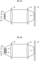
- Fig. 2A is a schematic diagram showing a configuration example of a photodetector 20 and an optical components disposed in a path of radiant light.
- the radiant light is emitted from the region corresponding to the beam spot 37 of the pulsed laser beam incident on the surface of the semiconductor wafer 35.
- the emitted radiant light is incident on the photodetector 20 through the two lenses 26.
- one of the two lenses 26 is disposed between the dichroic mirror 25 ( Fig. 1 ) and the semiconductor wafer 35, and the other is disposed between the dichroic mirror 25 and the photodetector 20.
- the two lenses 26 configure an imaging optical system that forms an image of a beam spot 37 on the surface of the semiconductor wafer 35 at a position where the photodetector 20 is disposed. That is, the surface of the semiconductor wafer 35 and the light receiving surface of the photodetector 20 are an object surface and an image surface, respectively.
- the photodetector 20 includes two light receiving units 21 that separately measure the intensity of radiant light.
- the two light receiving units 21 are disposed at different positions with respect to the longitudinal direction of the image 38 of the beam spot 37.
- the two light receiving units 21 each include an optical sensor 22 having a different peak sensitivity wavelength.
- Each of the optical sensors 22 outputs a signal (voltage) having the sensitivity in the infrared wavelength range and having a magnitude corresponding to the intensity of the input radiant light.
- the signals output from the two optical sensors 22 are input to the processing device 40.
- Fig. 2B is a schematic diagram showing another configuration example of a photodetector 20 and an optical components disposed in a path of radiant light.
- the two light receiving units 21 each include an optical sensor 22 having a different peak sensitivity wavelength.
- the two light receiving units 21 each include an optical sensor 22 having the same spectral sensitivity characteristic and a bandpass filter 23 having a different passing wavelength range. The radiant light transmitted through the bandpass filter 23 is incident on the optical sensor 22. Therefore, the peak sensitivity wavelengths of the two light receiving units 21 are different.
- Fig. 3 is a graph showing an example of a pulse of a pulsed laser beam output from the laser source 11 and an output signal waveform of two light receiving units 21 of the photodetector 20.
- the output value of the light receiving unit 21 gradually increases in response to the temperature increase of the outer layer portion of the semiconductor wafer 35.
- the output value of the light receiving unit 21 gradually decreases in response to the temperature decrease of the outer layer portion of the semiconductor wafer 35.
- the peak intensity Vp of the output of the light receiving unit 21 due to the laser pulse from time t1 to t2 is stored in the storage device 41 for each light receiving unit 21. Normally, this peak intensity Vp differs between the two light receiving units 21.
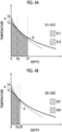
- Figs. 4A and 4B are graphs showing an example of temperature distribution in a depth direction at the time of falling edge of the laser pulse when a pulsed laser beam is incident on the semiconductor wafer 35.
- the horizontal axis of the graphs of Figs. 4A and 4B represents the depth from the surface of the semiconductor wafer 35, and the vertical axis represents the temperature.
- the solid line and the broken line in each of Figs. 4A and 4B respectively show the temperature distributions when a laser pulse having the same pulse energy and a relatively long pulse width and a laser pulse having a relatively short pulse width are incident.
- the shorter the pulse width the larger the peak power. Therefore, the temperature TS of the outermost surface (position of zero depth) when the pulse width is short is higher than the temperature TL of the outermost surface when the pulse width is long.
- the amount of heat conducted in the depth direction during the period during which the laser pulse is incident increases.
- the pulse width decreases the amount of heat conducted in the depth direction during the period during which the laser pulse is incident decreases.
- the deeper the depth from the surface, the lower the temperature, but the shorter the pulse width the smaller the amount of heat conducted in the depth direction, so that the degree of temperature decrease is greater when the pulse width is short. Therefore, in a region deeper than a certain depth Da, the temperature when the pulse width is long is higher than the temperature when the pulse width is short.
- the radiant light emitted from the outermost surface reaches the photodetector 20 without being absorbed by the semiconductor wafer 35.
- a part of the radiant light emitted from the deep region is absorbed by the semiconductor wafer 35 itself by the time the radiant light reaches the photodetector 20.
- the amount absorbed depends on the absorption coefficient of the semiconductor wafer 35. This absorption coefficient depends on the wavelength. The radiant light in the wavelength range having a large absorption coefficient is unlikely to be radiated from the deep region of the semiconductor wafer 35 to the outside.
- one light receiving unit 21 detects radiant light emitted from a region shallower than the depth D1 and the other light receiving unit 21 detects radiant light emitted from a region shallower than the depth D2 (D2 ⁇ D1).
- the detected value of the one light receiving unit 21 changes according to the area of the hatched portion in the region shallower than the depth D1.
- the detected value of the other light receiving unit 21 changes according to the area of the hatched portion in the region shallower than the depth D2.
- the area of the temperature distribution when the pulse width is short is larger than the area of the temperature distribution when the pulse width is long, and the difference is A.
- the area of the temperature distribution when the pulse width is long is larger than the area of the temperature distribution when the pulse width is short, and the difference is B.
- the area S11 of the graph of the temperature distribution when the pulse width is long and the area S12 of the graph of the temperature distribution when the pulse width is short are substantially equal. Therefore, it is not possible to distinguish between the temperature distribution of the solid line and the temperature distribution of the broken line in Fig. 4A only by the detected value of the light receiving unit 21 that detects the radiant light from the region having a depth shallower than D1. Therefore, it is difficult to accurately obtain the maximum ultimate temperature of the outermost surface of the semiconductor wafer 35.
- the area of the temperature distribution when the pulse width is long is larger than the area of the temperature distribution when the pulse width is short, and the difference is C.
- the area C is smaller than the area A. Therefore, the area S21 of the graph of the temperature distribution when the pulse width is long is smaller than the area S22 of the graph of the temperature distribution when the pulse width is short. Since the area S21 and the area S22 are different, it is possible to distinguish between the temperature distribution of the solid line and the temperature distribution of the broken line in Fig. 4B , based on the detected value of the light receiving unit 21 that detects the radiant light from the region having a depth shallower than D2.
- Figs. 5A to 5D are graphs showing the temperature distribution in the depth direction when the pulse width of the pulsed laser beam is constant and the pulse energies are different.
- the horizontal axis of the graphs of Figs. 5A to 5D represents the depth from the surface of the semiconductor wafer 35, and the vertical axis represents the temperature.
- Figs. 5A and 5B show the temperature distribution when one shot of a pulsed laser beam is incident under the condition of pulse energies E1 and E2 (E1 ⁇ E2) in which the temperature of the outermost surface of the semiconductor wafer 35 does not exceed the melting point.
- the temperature of the outermost surface is the highest, and the deeper the depth, the lower the temperature.
- the peak intensity Vp ( Fig. 3 ) of the signal output from the light receiving unit 21 that detects the radiant light from the region whose depth is shallower than D1 has a magnitude corresponding to the area S11 ( Fig. 5A ) when the pulse energy is E1, and has a magnitude corresponding to the sum of the area S11 ( Fig. 5A ) and the increment ⁇ S11 ( Fig. 5A ) when the pulse energy is E2.
- the peak intensity Vp ( Fig. 3 ) of the signal output from the light receiving unit 21 that detects the radiant light from the region whose depth is shallower than D2 has a magnitude corresponding to the area S21 ( Fig. 5B ) when the pulse energy is E1, and has a magnitude corresponding to the sum of the area S21 ( Fig. 5B ) and the increment ⁇ S21 ( Fig. 5B ) when the pulse energy is E2.
- Figs. 5C and 5D show the temperature distribution when one shot of a pulsed laser beam is incident under the condition of pulse energies E3 and E4 (E3 ⁇ E4) in which the temperature of the outermost surface of the semiconductor wafer 35 is equal to or higher than the melting point.
- the pulse energy is E3
- the temperature of the outermost surface of the semiconductor wafer 35 reaches the melting point.
- the pulse energy is E4 the outer layer portion of the semiconductor wafer 35 is melted.
- the temperature of the outermost surface is fixed to almost the melting point. Therefore, the temperature of the outermost surface is almost the same, when the pulse energy is E3 and when the pulse energy is E4. Since the temperature of the deep region where melting is not performed rises with the increase of the pulse energy, the temperature when the pulse energy is E4 is higher than the temperature when the pulse energy is E3.
- the peak intensity Vp ( Fig. 3 ) of the signal output from the light receiving unit 21 that detects the radiant light from the region whose depth is shallower than D1 has a magnitude corresponding to the area S11 ( Fig. 5C ) when the pulse energy is E3, and has a magnitude corresponding to the sum of the area S11 ( Fig. 5C ) and the increment ⁇ S11 ( Fig. 5C ) when the pulse energy is E4.
- the peak intensity Vp ( Fig. 3 ) of the signal output from the light receiving unit 21 that detects the radiant light from the region whose depth is shallower than D2 has a magnitude corresponding to the area S21 ( Fig.
- the ratio of the increment ⁇ S11 to the area S11 ( Fig. 5C ) and the ratio of the increment ⁇ S21 to the area S21 ( Fig. 5D ) is smaller than the ratio when the outermost surface does not melt ( Figs. 5A and 5B ) . That is, the slope of the change in the output value of the light receiving unit 21 with respect to the increase in pulse energy becomes gentle.
- the pulse energy when this slope starts to become gentle can be considered as the energy condition for the start of melting. In order to anneal the semiconductor wafer 35 at a temperature as high as possible under the condition where the semiconductor wafer 35 is not melted, it is desired to accurately find the energy condition where melting starts.
- Fig. 6 is a graph that approximates a curve of a scatter plot in which the output values of the two light receiving units 21 are plotted with respect to the pulse energy.
- the detected values of the light receiving units 21 that detect the radiant light from the regions having depths shallower than D1 and D2 are shown by a thick curve D1 and a thin curve D2, respectively.
- the ratios of the increments ⁇ S11 ( Fig. 5C ) and ⁇ S21 ( Fig. 5D ) to the areas S11 ( Fig. 5C ) and S21 ( Fig. 5D ) after the start of melting are smaller than the ratios of the increments ⁇ S11 ( Fig. 5A ) and ⁇ S21 ( Fig. 5B ) to the areas S11 ( Fig. 5A ) and S21 ( Fig. 5B ) before the start of melting, respectively. Therefore, when the pulse energy exceeds E1, the slope of the graph becomes gentle. However, the degree to which the ratio of the increment ⁇ S21 to the area S21 becomes smaller is larger than the degree to which the ratio of the increment ⁇ S11 to the area S11 becomes smaller. This is because the temperature rise is reduced in the region shallower than the depth D2. Therefore, in the graph shown in Fig. 6 , the degree to which the slope of the graph becomes gentle when the pulse energy exceeds E1 is larger in the curve D2 than in the curve D
- the pulse energy satisfying the condition where melting starts and the output values of the light receiving units 21 at that time can be specified more accurately, by comparing the changes in the output values of the two light receiving units 21 when the pulse energy is changed.
- the pulse energy E1 at the start of melting can be more accurately specified from the relationship between the pulse energy and the difference between the value shown by the curve D1 and the value shown by the curve D2 with respect to the pulse energy.
- the peak sensitivity wavelengths of the two light receiving units 21 may be set so as to satisfy the condition that the larger absorption coefficient is twice or more the smaller absorption coefficient.
- the peak sensitivity wavelength of the one light receiving unit 21 is a wavelength that is not transparent to silicon, for example, 1 um or less, in order to read the temperature information on the outermost surface.
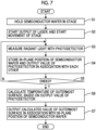
- Fig. 7 is a flowchart showing a procedure for performing laser annealing of the semiconductor wafer 35 by using a laser annealing device equipped with a process monitor according to an embodiment.
- the semiconductor wafer 35 ( Fig. 1 ) into which the dopant is injected is held in the stage 31 ( Fig. 1 ) (step S1) .
- This procedure is performed by, for example, a robot arm or the like.
- the stage 31 fixes the semiconductor wafer 35 by, for example, a vacuum chuck.
- step S2 After holding the semiconductor wafer 35 on the stage 31, the output of the pulsed laser beam from the laser source 11 and the movement of the stage 31 are started (step S2) . While scanning the semiconductor wafer 35 with the pulsed laser beam, the intensity of the radiant light from the semiconductor wafer 35 is measured by the photodetector 20 (step S3) . For example, the processing device 40 acquires the output value of the photodetector 20.
- the processing device 40 stores the in-plane position of the semiconductor wafer 35 on which the laser beam is incident and the output value of the photodetector 20 in the storage device 41 in association with each other (step S4).
- the processes of steps S3 and S4 are repeated until almost the entire surface of the semiconductor wafer 35 is annealed (step S5).
- the processing device 40 calculates the ultimate temperature of the outermost surface of the semiconductor wafer 35, based on the output value of the photodetector 20 (step S6). For example, the relationship between the output values of the two light receiving units 21 and the ultimate temperature of the outermost surface of the semiconductor wafer 35 is obtained in advance and is stored in the storage device 41.
- the processing device 40 outputs the calculated value of the ultimate temperature of the outermost surface of the semiconductor wafer 35 to the output device 42 ( Fig. 1 ) in association with the in-plane position of the semiconductor wafer 35.
- the distribution of the ultimate temperature in the plane of the semiconductor wafer 35 may be represented as a figure.
- the ultimate temperature of the outermost surface of the semiconductor wafer 35 can be obtained with higher accuracy. Therefore, it is possible to determine with high accuracy whether or not the outermost surface of the semiconductor wafer 35 is melted.
- the number of light receiving units 21 ( Figs. 2A and 2B ) included in the photodetector 20 is two, but the photodetector 20 may include a plurality of (three or more) light receiving units 21. Since three or more light receiving units 21 having different peak sensitivity wavelengths are disposed, the photodetector 20 can measure the intensities of radiant light in the plurality of (three or more) wavelength ranges. This makes it possible to improve accuracy of specifying the pulse energy satisfying the condition where melting starts and the output value of the light receiving unit 21 at that time.
- the ultimate temperature of the outermost surface of the semiconductor wafer 35 is obtained based on the measurement result of the photodetector 20, but it is also possible to obtain other physical quantities related to the semiconductor wafer 35 that change due to annealing. For example, by obtaining the relationship between the activation rate of the dopant, the sheet resistance, or the like and the measurement result of the photodetector 20 in advance, these physical quantities can be obtained based on the measurement result of the photodetector 20.
- the semiconductor wafer is to be annealed, but the process monitor according to the embodiment can also be used when a semiconductor member other than the semiconductor wafer is to be annealed.
- laser annealing is applied as an annealing method for the semiconductor wafer, but other annealing methods may be applied. For example, lamp annealing, furnace annealing, or the like may be applied.
- annealing is performed by a method that causes a temperature distribution in the depth direction, a particularly excellent effect can be obtained by using the process monitor according to the above embodiment.
Landscapes
- Physics & Mathematics (AREA)
- Spectroscopy & Molecular Physics (AREA)
- General Physics & Mathematics (AREA)
- Engineering & Computer Science (AREA)
- Optics & Photonics (AREA)
- Plasma & Fusion (AREA)
- Mechanical Engineering (AREA)
- Testing Or Measuring Of Semiconductors Or The Like (AREA)
- Electromagnetism (AREA)
- Health & Medical Sciences (AREA)
- Toxicology (AREA)
- Recrystallisation Techniques (AREA)
Abstract

Description
- The present invention relates to a process monitor and a process monitoring method for obtaining a physical quantity that changes due to annealing of a semiconductor member.
- In the related art, as an example of a method for identifying the in-plane distribution in the activated state of a semiconductor wafer in which a dopant is injected, and activated and annealed, sheet resistance has been measured. The activated state of the dopant can be evaluated from the in-plane distribution of the sheet resistance.
- [PTL 1]
Japanese Unexamined Patent Publication No. 2007-81348 - The four-point probe method is generally used to measure the sheet resistance. The measurement of sheet resistance by using the four-point probe method is performed after annealing with a device different from the activation annealing device. Therefore, the measurement of sheet resistance is an offline work, which is troublesome. In addition, the semiconductor wafer is damaged because the probe needs to be brought into contact with the semiconductor wafer. Further, in order to determine the quality of the annealing result, there is a request to measure the temperature of the semiconductor wafer being annealed.
- An object of the present invention is to provide a process monitor and a process monitoring method capable of measuring a physical quantity related to a semiconductor member that changes due to annealing without damaging the semiconductor member.
- According to an aspect of the present invention, there is provided a process monitor including:
- a photodetector that separately measures intensities of radiant light from a semiconductor member being annealed, in a plurality of wavelength ranges that are different from each other; and
- a processing device that obtains a physical quantity related to the semiconductor member that changes due to annealing, based on the intensities in the plurality of wavelength ranges measured by the photodetector.
- According to another aspect of the present invention, there is provided a process monitoring method including:
- annealing a semiconductor member;
- separately measuring intensities of radiant light from a semiconductor member being annealed, in a plurality of wavelength ranges that are different from each other; and
- obtaining a physical quantity related to the semiconductor member that changes due to annealing, based on a measurement result.
- Since the radiant light from the semiconductor member is detected and the physical quantity of the semiconductor member that changes due to annealing is obtained, the semiconductor member is not damaged. Further, by separately measuring the intensities of radiant light in a plurality of wavelength ranges, the measurement accuracy of physical quantities can be improved.
-
-
Fig. 1 is a schematic diagram of a laser annealing device equipped with a process monitor according to an embodiment. -
Fig. 2A is a schematic diagram showing a configuration example of a photodetector, and optical components disposed in a path of radiant light, andFig. 2B is a schematic diagram showing another configuration example of a photodetector and optical components disposed in the path of radiant light. -
Fig. 3 is a graph showing an example of a pulse of a pulsed laser beam output from a laser source and an output signal waveform of two light receiving units of a photodetector. -
Figs. 4A and 4B are graphs showing an example of temperature distribution in a depth direction when a pulsed laser beam is incident on a semiconductor wafer. -
Figs. 5A to 5D are graphs showing the temperature distribution in the depth direction when the pulse width of the pulsed laser beam is constant and the pulse energies are different. -
Fig. 6 is a graph that approximates a curve of a scatter plot in which an example of the output values of the two light receiving units is plotted with respect to the pulse energy. -
Fig. 7 is a flowchart showing a procedure for performing laser annealing of a semiconductor wafer by using a laser annealing device equipped with a process monitor according to an embodiment. - A process monitor and a process monitoring method according to the embodiment will be described with reference to
Figs. 1 to 7 . -
Fig. 1 is a schematic diagram of a laser annealing device equipped with a process monitor according to the embodiment. The laser annealing device includes a laseroptical system 10, achamber 30, aphotodetector 20, aprocessing device 40, astorage device 41, anoutput device 42, and aninput device 43. The function of the process monitor is implemented by thephotodetector 20, theprocessing device 40, and the like. - The laser
optical system 10 includes alaser source 11, a uniformizingoptical system 12, and afolding mirror 13. Thelaser source 11 outputs a laser beam in the infrared region. As thelaser source 11, for example, a laser diode having an oscillation wavelength of 808 nm can be used. The uniformizingoptical system 12 equalizes the beam profile of the laser beam output from thelaser source 11. Thefolding mirror 13 reflects the laser beam that has passed through the uniformizingoptical system 12 downward. - A
window 32 through which a laser beam is transmitted is provided on the top plate of thechamber 30, and astage 31 is disposed in thechamber 30. Thesemiconductor wafer 35, which is to be annealed, is held on thestage 31. A dopant is injected into the outer layer portion of thesemiconductor wafer 35. For the injection of the dopant, for example, the ion implantation method is used. Prior to annealing, the dopant is not activated. As the semiconductor wafer 35, for example, a silicon wafer can be used. As the dopant, for example, phosphorus (P), arsenic (As), boron (B), and the like can be used. - The laser beam output from the laser
optical system 10 transmits through thedichroic mirror 25 and thewindow 32 and is incident on thesemiconductor wafer 35 held on thestage 31. A mirror, a lens, or the like may be disposed in the path of the laser beam, if necessary. The beam spot of the laser beam on the surface of thesemiconductor wafer 35 has a long shape that is long in one direction, and is, for example, about 3 mm to 5 mm in length and about 0.1 mm to 0.3 mm in width. When the laser beam is incident on the semiconductor wafer 35, the outer layer portion of thesemiconductor wafer 35 is heated at the position of the beam spot. Thestage 31 is controlled by theprocessing device 40 to move thesemiconductor wafer 35 in two directions parallel to its surface. By scanning the beam spot on the surface of the semiconductor wafer 35 in the width direction and sub-scanning in the length direction, almost the entire upper surface of thesemiconductor wafer 35 can be laser-annealed. - When the laser beam is incident on the semiconductor wafer 35, the outer layer portion at the incident position is heated, so that the dopant is activated. The radiant light is emitted from the heated portion. A part of the radiant light emitted from the
semiconductor wafer 35 is reflected by thedichroic mirror 25 and incident on thephotodetector 20. Thedichroic mirror 25 transmits light in a wavelength range shorter than, for example, 1 µm, and reflects light in a wavelength range longer than 1 pm. If necessary, a lens, an optical filter, or the like may be disposed in the path of radiant light from thesemiconductor wafer 35 to thephotodetector 20. Thephotodetector 20 and the optical components on the path of radiant light will be described later with reference toFigs. 2A and 2B . - The
processing device 40 acquires a detection signal output from thephotodetector 20 in synchronization with each shot of the pulsed laser beam. Further, the magnitude (output value) of the acquired detection signal is stored in thestorage device 41 in association with in-plane position of thesemiconductor wafer 35. As an example, for each shot of the pulsed laser beam, the temporal waveform of the output value is obtained corresponding to the temporal change of the intensity of the radiant light. The output value stored in thestorage device 41 is, for example, the peak value of the temporal waveform of the pulsed laser beam for each shot. - Various commands and data for instructing the operations of the process monitor and the laser annealing device are input to the
processing device 40 through theinput device 43. Theprocessing device 40 outputs the monitor result from the process monitor to theoutput device 42. -
Fig. 2A is a schematic diagram showing a configuration example of aphotodetector 20 and an optical components disposed in a path of radiant light. The radiant light is emitted from the region corresponding to thebeam spot 37 of the pulsed laser beam incident on the surface of thesemiconductor wafer 35. The emitted radiant light is incident on thephotodetector 20 through the twolenses 26. For example, one of the twolenses 26 is disposed between the dichroic mirror 25 (Fig. 1 ) and thesemiconductor wafer 35, and the other is disposed between thedichroic mirror 25 and thephotodetector 20. The twolenses 26 configure an imaging optical system that forms an image of abeam spot 37 on the surface of thesemiconductor wafer 35 at a position where thephotodetector 20 is disposed. That is, the surface of thesemiconductor wafer 35 and the light receiving surface of thephotodetector 20 are an object surface and an image surface, respectively. - The
photodetector 20 includes twolight receiving units 21 that separately measure the intensity of radiant light. The twolight receiving units 21 are disposed at different positions with respect to the longitudinal direction of theimage 38 of thebeam spot 37. The twolight receiving units 21 each include anoptical sensor 22 having a different peak sensitivity wavelength. Each of theoptical sensors 22 outputs a signal (voltage) having the sensitivity in the infrared wavelength range and having a magnitude corresponding to the intensity of the input radiant light. The signals output from the twooptical sensors 22 are input to theprocessing device 40. -
Fig. 2B is a schematic diagram showing another configuration example of aphotodetector 20 and an optical components disposed in a path of radiant light. In the configuration example shown inFig. 2A , the twolight receiving units 21 each include anoptical sensor 22 having a different peak sensitivity wavelength. On the other hand, in the configuration example shown inFig. 2B , the twolight receiving units 21 each include anoptical sensor 22 having the same spectral sensitivity characteristic and abandpass filter 23 having a different passing wavelength range. The radiant light transmitted through thebandpass filter 23 is incident on theoptical sensor 22. Therefore, the peak sensitivity wavelengths of the twolight receiving units 21 are different. -
Fig. 3 is a graph showing an example of a pulse of a pulsed laser beam output from thelaser source 11 and an output signal waveform of twolight receiving units 21 of thephotodetector 20. When the laser pulse rises at time t1, the output value of thelight receiving unit 21 gradually increases in response to the temperature increase of the outer layer portion of thesemiconductor wafer 35. When the laser pulse falls at time t2, the output value of thelight receiving unit 21 gradually decreases in response to the temperature decrease of the outer layer portion of thesemiconductor wafer 35. The peak intensity Vp of the output of thelight receiving unit 21 due to the laser pulse from time t1 to t2 is stored in thestorage device 41 for each light receivingunit 21. Normally, this peak intensity Vp differs between the twolight receiving units 21. - Next, the excellent effects of the present embodiment will be described with reference to
Figs. 4A to 5D . -
Figs. 4A and 4B are graphs showing an example of temperature distribution in a depth direction at the time of falling edge of the laser pulse when a pulsed laser beam is incident on thesemiconductor wafer 35. The horizontal axis of the graphs ofFigs. 4A and 4B represents the depth from the surface of thesemiconductor wafer 35, and the vertical axis represents the temperature. The solid line and the broken line in each ofFigs. 4A and 4B respectively show the temperature distributions when a laser pulse having the same pulse energy and a relatively long pulse width and a laser pulse having a relatively short pulse width are incident. - When the pulse energies are the same, the shorter the pulse width, the larger the peak power. Therefore, the temperature TS of the outermost surface (position of zero depth) when the pulse width is short is higher than the temperature TL of the outermost surface when the pulse width is long. As the pulse width increases, the amount of heat conducted in the depth direction during the period during which the laser pulse is incident increases. On the contrary, when the pulse width decreases, the amount of heat conducted in the depth direction during the period during which the laser pulse is incident decreases. Regardless of the pulse width, the deeper the depth from the surface, the lower the temperature, but the shorter the pulse width, the smaller the amount of heat conducted in the depth direction, so that the degree of temperature decrease is greater when the pulse width is short. Therefore, in a region deeper than a certain depth Da, the temperature when the pulse width is long is higher than the temperature when the pulse width is short.
- The radiant light emitted from the outermost surface reaches the
photodetector 20 without being absorbed by thesemiconductor wafer 35. On the other hand, a part of the radiant light emitted from the deep region is absorbed by thesemiconductor wafer 35 itself by the time the radiant light reaches thephotodetector 20. The amount absorbed depends on the absorption coefficient of thesemiconductor wafer 35. This absorption coefficient depends on the wavelength. The radiant light in the wavelength range having a large absorption coefficient is unlikely to be radiated from the deep region of thesemiconductor wafer 35 to the outside. - In the following description, the absorption phenomenon of radiant light is simplified, it is assumed that one
light receiving unit 21 detects radiant light emitted from a region shallower than the depth D1 and the otherlight receiving unit 21 detects radiant light emitted from a region shallower than the depth D2 (D2 < D1). - As shown in
Fig. 4A , the detected value of the onelight receiving unit 21 changes according to the area of the hatched portion in the region shallower than the depth D1. As shown inFig. 4B , the detected value of the otherlight receiving unit 21 changes according to the area of the hatched portion in the region shallower than the depth D2. - In the example shown in
Fig. 4A , in the region where the depth is shallower than Da, the area of the temperature distribution when the pulse width is short is larger than the area of the temperature distribution when the pulse width is long, and the difference is A. In the region where the depth is from Da to D1, conversely, the area of the temperature distribution when the pulse width is long is larger than the area of the temperature distribution when the pulse width is short, and the difference is B. When the area A and the area B are equal, the area S11 of the graph of the temperature distribution when the pulse width is long and the area S12 of the graph of the temperature distribution when the pulse width is short are substantially equal. Therefore, it is not possible to distinguish between the temperature distribution of the solid line and the temperature distribution of the broken line inFig. 4A only by the detected value of thelight receiving unit 21 that detects the radiant light from the region having a depth shallower than D1. Therefore, it is difficult to accurately obtain the maximum ultimate temperature of the outermost surface of thesemiconductor wafer 35. - On the other hand, in the example shown in
Fig. 4B , in the region where the depth is from Da to D2, the area of the temperature distribution when the pulse width is long is larger than the area of the temperature distribution when the pulse width is short, and the difference is C. The area C is smaller than the area A. Therefore, the area S21 of the graph of the temperature distribution when the pulse width is long is smaller than the area S22 of the graph of the temperature distribution when the pulse width is short. Since the area S21 and the area S22 are different, it is possible to distinguish between the temperature distribution of the solid line and the temperature distribution of the broken line inFig. 4B , based on the detected value of thelight receiving unit 21 that detects the radiant light from the region having a depth shallower than D2. - As in the present embodiment, by separately measuring the intensities of radiant light in different wavelength ranges with the two
light receiving units 21, it becomes possible to measure more accurately the temperature of the outermost surface of thesemiconductor wafer 35 when the temperature distribution in the depth direction is different. -
Figs. 5A to 5D are graphs showing the temperature distribution in the depth direction when the pulse width of the pulsed laser beam is constant and the pulse energies are different. The horizontal axis of the graphs ofFigs. 5A to 5D represents the depth from the surface of thesemiconductor wafer 35, and the vertical axis represents the temperature. -
Figs. 5A and 5B show the temperature distribution when one shot of a pulsed laser beam is incident under the condition of pulse energies E1 and E2 (E1 < E2) in which the temperature of the outermost surface of thesemiconductor wafer 35 does not exceed the melting point. The temperature of the outermost surface is the highest, and the deeper the depth, the lower the temperature. When the pulse energy increases from E1 to E2, the temperature at each depth of thesemiconductor wafer 35 rises, but the shape of the temperature distribution is almost maintained. - The peak intensity Vp (
Fig. 3 ) of the signal output from thelight receiving unit 21 that detects the radiant light from the region whose depth is shallower than D1 has a magnitude corresponding to the area S11 (Fig. 5A ) when the pulse energy is E1, and has a magnitude corresponding to the sum of the area S11 (Fig. 5A ) and the increment ΔS11 (Fig. 5A ) when the pulse energy is E2. The peak intensity Vp (Fig. 3 ) of the signal output from thelight receiving unit 21 that detects the radiant light from the region whose depth is shallower than D2 has a magnitude corresponding to the area S21 (Fig. 5B ) when the pulse energy is E1, and has a magnitude corresponding to the sum of the area S21 (Fig. 5B ) and the increment ΔS21 (Fig. 5B ) when the pulse energy is E2. -
Figs. 5C and 5D show the temperature distribution when one shot of a pulsed laser beam is incident under the condition of pulse energies E3 and E4 (E3 < E4) in which the temperature of the outermost surface of thesemiconductor wafer 35 is equal to or higher than the melting point. Under the condition that the pulse energy is E3, the temperature of the outermost surface of thesemiconductor wafer 35 reaches the melting point. Under the condition that the pulse energy is E4, the outer layer portion of thesemiconductor wafer 35 is melted. When the outer layer portion of thesemiconductor wafer 35 begins to melt, the temperature of the outermost surface is fixed to almost the melting point. Therefore, the temperature of the outermost surface is almost the same, when the pulse energy is E3 and when the pulse energy is E4. Since the temperature of the deep region where melting is not performed rises with the increase of the pulse energy, the temperature when the pulse energy is E4 is higher than the temperature when the pulse energy is E3. - The peak intensity Vp (
Fig. 3 ) of the signal output from thelight receiving unit 21 that detects the radiant light from the region whose depth is shallower than D1 has a magnitude corresponding to the area S11 (Fig. 5C ) when the pulse energy is E3, and has a magnitude corresponding to the sum of the area S11 (Fig. 5C ) and the increment ΔS11 (Fig. 5C ) when the pulse energy is E4. The peak intensity Vp (Fig. 3 ) of the signal output from thelight receiving unit 21 that detects the radiant light from the region whose depth is shallower than D2 has a magnitude corresponding to the area S21 (Fig. 5D ) when the pulse energy is E3, and has a magnitude corresponding to the sum of the area S21 (Fig. 5D ) and the increment ΔS21 (Fig. 5D ) when the pulse energy is E4. Here, for the sake of simplicity, the difference between the emissivity from the semiconductor in the molten state and the emissivity from the semiconductor in the solid state is not considered. - When the outermost surface of the
semiconductor wafer 35 begins to melt, the temperature of the outermost surface hardly rises even when the pulse energy is increased. Therefore, the ratio of the increment ΔS11 to the area S11 (Fig. 5C ) and the ratio of the increment ΔS21 to the area S21 (Fig. 5D ) is smaller than the ratio when the outermost surface does not melt (Figs. 5A and 5B ) . That is, the slope of the change in the output value of thelight receiving unit 21 with respect to the increase in pulse energy becomes gentle. The pulse energy when this slope starts to become gentle can be considered as the energy condition for the start of melting. In order to anneal thesemiconductor wafer 35 at a temperature as high as possible under the condition where thesemiconductor wafer 35 is not melted, it is desired to accurately find the energy condition where melting starts. -
Fig. 6 is a graph that approximates a curve of a scatter plot in which the output values of the twolight receiving units 21 are plotted with respect to the pulse energy. The detected values of thelight receiving units 21 that detect the radiant light from the regions having depths shallower than D1 and D2 are shown by a thick curve D1 and a thin curve D2, respectively. - In the scatter plot shown in
Fig. 6 , it is assumed that melting starts under the condition that the pulse energy is E1. The slopes of the graphs change near the condition where melting starts, but no clear bend point appears. Therefore, it is difficult to accurately find the condition where melting starts, from the measurement result of onelight receiving unit 21. - The ratios of the increments ΔS11 (
Fig. 5C ) and ΔS21 (Fig. 5D ) to the areas S11 (Fig. 5C ) and S21 (Fig. 5D ) after the start of melting are smaller than the ratios of the increments ΔS11 (Fig. 5A ) and ΔS21 (Fig. 5B ) to the areas S11 (Fig. 5A ) and S21 (Fig. 5B ) before the start of melting, respectively. Therefore, when the pulse energy exceeds E1, the slope of the graph becomes gentle. However, the degree to which the ratio of the increment ΔS21 to the area S21 becomes smaller is larger than the degree to which the ratio of the increment ΔS11 to the area S11 becomes smaller. This is because the temperature rise is reduced in the region shallower than the depth D2. Therefore, in the graph shown inFig. 6 , the degree to which the slope of the graph becomes gentle when the pulse energy exceeds E1 is larger in the curve D2 than in the curve D1. - Since the degree to which the slope becomes gentle differs between the curve D1 and the curve D2, the pulse energy satisfying the condition where melting starts and the output values of the
light receiving units 21 at that time can be specified more accurately, by comparing the changes in the output values of the twolight receiving units 21 when the pulse energy is changed. For example, the pulse energy E1 at the start of melting can be more accurately specified from the relationship between the pulse energy and the difference between the value shown by the curve D1 and the value shown by the curve D2 with respect to the pulse energy. - In order to improve accuracy of specifying the pulse energy satisfying the condition where melting starts and the output value of the
light receiving unit 21 at that time, it is preferable to increase the difference in the absorption coefficient of thesemiconductor wafer 35 at the peak sensitivity wavelengths of the twolight receiving units 21. For example, the peak sensitivity wavelengths of the twolight receiving units 21 may be set so as to satisfy the condition that the larger absorption coefficient is twice or more the smaller absorption coefficient. - When the
semiconductor wafer 35 is made of silicon, it is preferable that the peak sensitivity wavelength of the onelight receiving unit 21 is a wavelength that is not transparent to silicon, for example, 1 um or less, in order to read the temperature information on the outermost surface. For example, it is preferable to set the wavelength range of visible light having a wavelength of 400 nm or more and 800 nm or less or the wavelength range of near infrared rays having a wavelength of about 900 nm. -
Fig. 7 is a flowchart showing a procedure for performing laser annealing of thesemiconductor wafer 35 by using a laser annealing device equipped with a process monitor according to an embodiment. - First, the semiconductor wafer 35 (
Fig. 1 ) into which the dopant is injected is held in the stage 31 (Fig. 1 ) (step S1) . This procedure is performed by, for example, a robot arm or the like. Thestage 31 fixes thesemiconductor wafer 35 by, for example, a vacuum chuck. - After holding the
semiconductor wafer 35 on thestage 31, the output of the pulsed laser beam from thelaser source 11 and the movement of thestage 31 are started (step S2) . While scanning thesemiconductor wafer 35 with the pulsed laser beam, the intensity of the radiant light from thesemiconductor wafer 35 is measured by the photodetector 20 (step S3) . For example, theprocessing device 40 acquires the output value of thephotodetector 20. - The
processing device 40 stores the in-plane position of thesemiconductor wafer 35 on which the laser beam is incident and the output value of thephotodetector 20 in thestorage device 41 in association with each other (step S4). The processes of steps S3 and S4 are repeated until almost the entire surface of thesemiconductor wafer 35 is annealed (step S5). - When the annealing of almost the entire surface of the
semiconductor wafer 35 is completed, theprocessing device 40 calculates the ultimate temperature of the outermost surface of thesemiconductor wafer 35, based on the output value of the photodetector 20 (step S6). For example, the relationship between the output values of the twolight receiving units 21 and the ultimate temperature of the outermost surface of thesemiconductor wafer 35 is obtained in advance and is stored in thestorage device 41. Theprocessing device 40 outputs the calculated value of the ultimate temperature of the outermost surface of thesemiconductor wafer 35 to the output device 42 (Fig. 1 ) in association with the in-plane position of thesemiconductor wafer 35. For example, the distribution of the ultimate temperature in the plane of thesemiconductor wafer 35 may be represented as a figure. - By using the process monitor according to the above embodiment, the ultimate temperature of the outermost surface of the
semiconductor wafer 35 can be obtained with higher accuracy. Therefore, it is possible to determine with high accuracy whether or not the outermost surface of thesemiconductor wafer 35 is melted. - Next, a modification example of the above embodiment will be described.
- In the above embodiment, the number of light receiving units 21 (
Figs. 2A and 2B ) included in thephotodetector 20 is two, but thephotodetector 20 may include a plurality of (three or more)light receiving units 21. Since three or more light receivingunits 21 having different peak sensitivity wavelengths are disposed, thephotodetector 20 can measure the intensities of radiant light in the plurality of (three or more) wavelength ranges. This makes it possible to improve accuracy of specifying the pulse energy satisfying the condition where melting starts and the output value of thelight receiving unit 21 at that time. - In the above embodiment, the ultimate temperature of the outermost surface of the
semiconductor wafer 35 is obtained based on the measurement result of thephotodetector 20, but it is also possible to obtain other physical quantities related to thesemiconductor wafer 35 that change due to annealing. For example, by obtaining the relationship between the activation rate of the dopant, the sheet resistance, or the like and the measurement result of thephotodetector 20 in advance, these physical quantities can be obtained based on the measurement result of thephotodetector 20. - In the above embodiment, the semiconductor wafer is to be annealed, but the process monitor according to the embodiment can also be used when a semiconductor member other than the semiconductor wafer is to be annealed. Further, in the above embodiment, laser annealing is applied as an annealing method for the semiconductor wafer, but other annealing methods may be applied. For example, lamp annealing, furnace annealing, or the like may be applied. When annealing is performed by a method that causes a temperature distribution in the depth direction, a particularly excellent effect can be obtained by using the process monitor according to the above embodiment.
- Needless to say, the above-described embodiment is merely an example, and partial replacement or combination of the configurations shown in the embodiment and modification example is possible. The same effects due to the same configurations of the embodiment and modification example will not be sequentially described for each of the embodiment and modification example. Further, the present invention is not limited to the above-described embodiment. For example, it will be apparent to those skilled in the art that various modifications, improvements, combinations, or the like can be made.
-
- 10
- Laser optical system
- 11
- Laser source
- 12
- Uniformizing optical system
- 13
- Folding mirror
- 20
- Photodetector
- 21
- Light receiving unit
- 22
- Optical sensor
- 23
- Bandpass filter
- 25
- Dichroic mirror
- 26
- Lens
- 30
- Chamber
- 31
- Stage
- 32
- Window
- 35
- Semiconductor wafer
- 37
- Beam spot
- 38
- Beam spot image
- 40
- Processing device
- 41
- Storage device
- 42
- Output device
- 43
- Input device
Claims (7)
- A process monitor comprising:a photodetector that separately measures intensities of radiant light from a semiconductor member being annealed, in a plurality of wavelength ranges that are different from each other; anda processing device that obtains a physical quantity related to the semiconductor member that changes due to annealing, based on the intensities in the plurality of wavelength ranges measured by the photodetector.
- The process monitor according to claim 1, whereinthe photodetector detects radiant light from the semiconductor member whose outer layer portion is heated by input of a laser beam, andthe processing device obtains an ultimate temperature of an outermost surface of the semiconductor member, as the physical quantity related to the semiconductor member that changes due to annealing.
- The process monitor according to claim 2, whereina beam spot of a laser beam on a surface of the semiconductor member has a long shape that is long in one direction,the photodetector includes a plurality of light receiving units that separately measure the intensities of radiant light in the plurality of wavelength ranges,the process monitor further comprises an imaging optical system that forms an image on the surface of the semiconductor member, andthe plurality of light receiving units are disposed at different positions in a longitudinal direction of the image of the beam spot on the surface of the semiconductor member, the image being formed by the imaging optical system.
- The process monitor according to any one of claims 1 to 3, wherein
the plurality of light receiving units each include an optical sensor having a different peak sensitivity wavelength. - The process monitor according to any one of claims 1 to 3, wherein
the plurality of light receiving units each include an optical sensor having the same spectral sensitivity characteristic, and a bandpass filter having a different passing wavelength range, and radiant light transmitted through the bandpass filter is incident on the optical sensor. - A process monitoring method comprising:annealing a semiconductor member;separately measuring intensities of radiant light from a semiconductor member being annealed, in a plurality of wavelength ranges that are different from each other; andobtaining a physical quantity related to the semiconductor member that changes due to annealing, based on a measurement result.
- The process monitoring method according to claim 6, whereinthe annealing of the semiconductor member is performed by inputting a laser beam to the semiconductor member, andan ultimate temperature of an outermost surface of the semiconductor member is obtained as the physical quantity related to the semiconductor member.
Applications Claiming Priority (2)
| Application Number | Priority Date | Filing Date | Title |
|---|---|---|---|
| JP2020052662 | 2020-03-24 | ||
| PCT/JP2021/007107 WO2021192801A1 (en) | 2020-03-24 | 2021-02-25 | Process monitor and process monitoring method |
Publications (2)
| Publication Number | Publication Date |
|---|---|
| EP4131340A1 true EP4131340A1 (en) | 2023-02-08 |
| EP4131340A4 EP4131340A4 (en) | 2023-10-25 |
Family
ID=77891655
Family Applications (1)
| Application Number | Title | Priority Date | Filing Date |
|---|---|---|---|
| EP21777149.2A Pending EP4131340A4 (en) | 2020-03-24 | 2021-02-25 | PROCESS MONITOR AND PROCESS MONITORING METHOD |
Country Status (6)
| Country | Link |
|---|---|
| US (1) | US12424469B2 (en) |
| EP (1) | EP4131340A4 (en) |
| JP (1) | JP7597792B2 (en) |
| KR (1) | KR102836193B1 (en) |
| CN (1) | CN115298802B (en) |
| WO (1) | WO2021192801A1 (en) |
Family Cites Families (26)
| Publication number | Priority date | Publication date | Assignee | Title |
|---|---|---|---|---|
| GB1463886A (en) * | 1973-06-29 | 1977-02-09 | Hughes Aircraft Co | Processes for fabricating monolithic optoelectronic semicon ductor devices |
| JPS60131430A (en) * | 1983-12-19 | 1985-07-13 | Dainippon Screen Mfg Co Ltd | Semiconductor substrate temperature measurement device |
| US5061084A (en) * | 1988-04-27 | 1991-10-29 | Ag Processing Technologies, Inc. | Pyrometer apparatus and method |
| JPH0936489A (en) * | 1995-07-21 | 1997-02-07 | Rohm Co Ltd | Measuring method for optical semiconductor element |
| JPH11297973A (en) * | 1998-04-07 | 1999-10-29 | Mitsubishi Electric Corp | Infrared imaging device |
| US6555457B1 (en) * | 2000-04-07 | 2003-04-29 | Triquint Technology Holding Co. | Method of forming a laser circuit having low penetration ohmic contact providing impurity gettering and the resultant laser circuit |
| US9952161B2 (en) * | 2001-12-06 | 2018-04-24 | Attofemto, Inc. | Methods for obtaining and analyzing digital interferometric data for computer testing and developing semiconductor and anisotropic devices and materials |
| US6917039B2 (en) * | 2002-02-13 | 2005-07-12 | Therma-Wave, Inc. | Method and system for combined photothermal modulated reflectance and photothermal IR radiometric system |
| JP2003318121A (en) * | 2002-04-26 | 2003-11-07 | Trecenti Technologies Inc | Method for manufacturing semiconductor device |
| US7280215B2 (en) * | 2003-09-24 | 2007-10-09 | Therma-Wave, Inc. | Photothermal system with spectroscopic pump and probe |
| JP2007081348A (en) | 2005-09-16 | 2007-03-29 | Matsushita Electric Ind Co Ltd | Heat treatment temperature adjustment method, substrate heat treatment method, and substrate heat treatment apparatus |
| JP5006560B2 (en) * | 2006-03-27 | 2012-08-22 | 大阪瓦斯株式会社 | Temperature detection method, temperature detection device, and cooking device provided with temperature detection device |
| US7398693B2 (en) * | 2006-03-30 | 2008-07-15 | Applied Materials, Inc. | Adaptive control method for rapid thermal processing of a substrate |
| US7705977B2 (en) * | 2006-12-21 | 2010-04-27 | Kla-Tencor Corporation | Methods for depth profiling in semiconductors using modulated optical reflectance technology |
| JP5507102B2 (en) * | 2009-03-19 | 2014-05-28 | 大日本スクリーン製造株式会社 | Heat treatment apparatus and heat treatment method |
| KR102038720B1 (en) * | 2011-12-07 | 2019-10-30 | 어플라이드 머티어리얼스, 인코포레이티드 | Laser reflectometry for substrate processing |
| US8871605B2 (en) * | 2012-04-18 | 2014-10-28 | Taiwan Semiconductor Manufacturing Co., Ltd. | Methods for fabricating and orienting semiconductor wafers |
| JP5963701B2 (en) * | 2013-03-27 | 2016-08-03 | 住友重機械工業株式会社 | Semiconductor annealing apparatus and temperature measuring method |
| CN106783536B (en) * | 2016-11-29 | 2021-11-30 | 京东方科技集团股份有限公司 | Laser annealing equipment, polycrystalline silicon thin film and preparation method of thin film transistor |
| KR102342848B1 (en) * | 2017-04-21 | 2021-12-23 | 삼성전자주식회사 | Laser annealing apparatus |
| US10418238B2 (en) * | 2017-05-12 | 2019-09-17 | Ohio State Innovation Foundation | Devices, systems, and methods for light emission and detection using amorphous silicon |
| JP6957099B2 (en) * | 2017-09-05 | 2021-11-02 | 住友重機械工業株式会社 | Laser annealing device and sheet resistance calculation device |
| KR102180311B1 (en) * | 2018-07-27 | 2020-11-18 | 주식회사 코윈디에스티 | Laser annealing apparatus |
| TWI776371B (en) * | 2020-01-30 | 2022-09-01 | 漢辰科技股份有限公司 | Method for controlling wafer temperature in an ion implantation system having an ion implanter and a processing station, non-transitory computer-readable storage medium storing one or more programs and ion implantation system |
| WO2023190563A1 (en) * | 2022-03-31 | 2023-10-05 | 古河電気工業株式会社 | Laser cutting method and laser cutting device |
| JP2025131430A (en) | 2024-02-28 | 2025-09-09 | Necプラットフォームズ株式会社 | Sound source generating device, sound source generating method, and sound source generating program. |
-
2021
- 2021-02-25 WO PCT/JP2021/007107 patent/WO2021192801A1/en not_active Ceased
- 2021-02-25 JP JP2022509437A patent/JP7597792B2/en active Active
- 2021-02-25 EP EP21777149.2A patent/EP4131340A4/en active Pending
- 2021-02-25 CN CN202180022297.XA patent/CN115298802B/en active Active
- 2021-02-25 KR KR1020227035868A patent/KR102836193B1/en active Active
-
2022
- 2022-09-17 US US17/933,095 patent/US12424469B2/en active Active
Also Published As
| Publication number | Publication date |
|---|---|
| WO2021192801A1 (en) | 2021-09-30 |
| KR20220157995A (en) | 2022-11-29 |
| US20230011199A1 (en) | 2023-01-12 |
| KR102836193B1 (en) | 2025-07-17 |
| JP7597792B2 (en) | 2024-12-10 |
| US12424469B2 (en) | 2025-09-23 |
| EP4131340A4 (en) | 2023-10-25 |
| CN115298802A (en) | 2022-11-04 |
| CN115298802B (en) | 2025-10-28 |
| JPWO2021192801A1 (en) | 2021-09-30 |
Similar Documents
| Publication | Publication Date | Title |
|---|---|---|
| JP5105903B2 (en) | Laser annealing apparatus and annealing method | |
| EP2210696A1 (en) | Method and apparatus for irradiating a semiconductor material surface by laser energy | |
| US20140314121A1 (en) | Optical non-destructive inspection apparatus and optical non-destructive inspection method | |
| EP2796858A1 (en) | Optical non-destructive inspection apparatus and optical non-destructive inspection method | |
| US12106983B2 (en) | Annealing device and annealing method | |
| WO2018142958A1 (en) | Heat treatment device, heat treatment method, and method for manufacturing semiconductor device | |
| JP2024001046A (en) | Laser power control device, laser processing device and laser power control method | |
| JP6294312B2 (en) | Laser power sensor | |
| US20180283957A1 (en) | Apparatus and method to measure temperature of 3d semiconductor structures via laser diffraction | |
| US20140339429A1 (en) | Optical non-destructive inspection method and optical non-destructive inspection apparatus | |
| JP6809952B2 (en) | Laser processing equipment | |
| EP2796857A1 (en) | Optical non-destructive inspection apparatus and optical non-destructive inspection method | |
| US12424469B2 (en) | Process monitor and process monitoring method | |
| KR102337481B1 (en) | Chuck plate, annealing apparatus, and annealing method | |
| JP5071961B2 (en) | Laser annealing apparatus, annealing method, and melt depth measuring apparatus | |
| KR20210147009A (en) | Non-contact temperature sensor | |
| EP3451370B1 (en) | Laser annealing apparatus and sheet resistance calculation apparatus | |
| KR102258055B1 (en) | Temperature monitoring system of laser annealing equipment | |
| US20220238394A1 (en) | Temperature control method, temperature control device, and optical heating device | |
| JP6976658B2 (en) | Chuck plate and annealing equipment | |
| JP2018132389A (en) | Wafer position measuring device and method for measuring wafer position | |
| KR20250111561A (en) | Laser heat treatment device for providing high-speed temperature monitoring |
Legal Events
| Date | Code | Title | Description |
|---|---|---|---|
| STAA | Information on the status of an ep patent application or granted ep patent |
Free format text: STATUS: THE INTERNATIONAL PUBLICATION HAS BEEN MADE |
|
| PUAI | Public reference made under article 153(3) epc to a published international application that has entered the european phase |
Free format text: ORIGINAL CODE: 0009012 |
|
| STAA | Information on the status of an ep patent application or granted ep patent |
Free format text: STATUS: REQUEST FOR EXAMINATION WAS MADE |
|
| 17P | Request for examination filed |
Effective date: 20220915 |
|
| AK | Designated contracting states |
Kind code of ref document: A1 Designated state(s): AL AT BE BG CH CY CZ DE DK EE ES FI FR GB GR HR HU IE IS IT LI LT LU LV MC MK MT NL NO PL PT RO RS SE SI SK SM TR |
|
| DAV | Request for validation of the european patent (deleted) | ||
| DAX | Request for extension of the european patent (deleted) | ||
| STAA | Information on the status of an ep patent application or granted ep patent |
Free format text: STATUS: EXAMINATION IS IN PROGRESS |
|
| A4 | Supplementary search report drawn up and despatched |
Effective date: 20230927 |
|
| RIC1 | Information provided on ipc code assigned before grant |
Ipc: H01L 21/67 20060101ALI20230921BHEP Ipc: G01J 5/60 20060101ALI20230921BHEP Ipc: G01J 5/00 20220101ALI20230921BHEP Ipc: H01L 21/268 20060101ALI20230921BHEP Ipc: H01L 21/265 20060101AFI20230921BHEP |
|
| 17Q | First examination report despatched |
Effective date: 20231010 |