EP4131333A1 - Electron tube, electron tube module, and optical device - Google Patents
Electron tube, electron tube module, and optical device Download PDFInfo
- Publication number
- EP4131333A1 EP4131333A1 EP21841496.9A EP21841496A EP4131333A1 EP 4131333 A1 EP4131333 A1 EP 4131333A1 EP 21841496 A EP21841496 A EP 21841496A EP 4131333 A1 EP4131333 A1 EP 4131333A1
- Authority
- EP
- European Patent Office
- Prior art keywords
- light
- electron tube
- photocathode
- light incident
- prism
- Prior art date
- Legal status (The legal status is an assumption and is not a legal conclusion. Google has not performed a legal analysis and makes no representation as to the accuracy of the status listed.)
- Pending
Links
- 230000003287 optical effect Effects 0.000 title claims description 61
- 239000000758 substrate Substances 0.000 claims abstract description 68
- 238000001514 detection method Methods 0.000 claims description 80
- 239000004065 semiconductor Substances 0.000 claims description 12
- 238000005259 measurement Methods 0.000 claims description 10
- 230000004044 response Effects 0.000 claims description 6
- 230000001678 irradiating effect Effects 0.000 claims description 5
- 239000000523 sample Substances 0.000 description 28
- 230000005284 excitation Effects 0.000 description 23
- 230000004048 modification Effects 0.000 description 17
- 238000012986 modification Methods 0.000 description 17
- 239000000463 material Substances 0.000 description 14
- 239000000853 adhesive Substances 0.000 description 10
- 230000001070 adhesive effect Effects 0.000 description 10
- 229910052751 metal Inorganic materials 0.000 description 9
- 239000002184 metal Substances 0.000 description 9
- 238000010521 absorption reaction Methods 0.000 description 8
- 230000000694 effects Effects 0.000 description 7
- 238000000034 method Methods 0.000 description 7
- 239000013307 optical fiber Substances 0.000 description 6
- 238000010586 diagram Methods 0.000 description 5
- 238000005520 cutting process Methods 0.000 description 4
- 239000011521 glass Substances 0.000 description 4
- 230000008569 process Effects 0.000 description 4
- 230000005540 biological transmission Effects 0.000 description 3
- 238000005219 brazing Methods 0.000 description 3
- 230000000630 rising effect Effects 0.000 description 3
- XKRFYHLGVUSROY-UHFFFAOYSA-N Argon Chemical compound [Ar] XKRFYHLGVUSROY-UHFFFAOYSA-N 0.000 description 2
- 229910001218 Gallium arsenide Inorganic materials 0.000 description 2
- 229910000530 Gallium indium arsenide Inorganic materials 0.000 description 2
- 238000001069 Raman spectroscopy Methods 0.000 description 2
- VYPSYNLAJGMNEJ-UHFFFAOYSA-N Silicium dioxide Chemical compound O=[Si]=O VYPSYNLAJGMNEJ-UHFFFAOYSA-N 0.000 description 2
- BQCADISMDOOEFD-UHFFFAOYSA-N Silver Chemical compound [Ag] BQCADISMDOOEFD-UHFFFAOYSA-N 0.000 description 2
- GWEVSGVZZGPLCZ-UHFFFAOYSA-N Titan oxide Chemical compound O=[Ti]=O GWEVSGVZZGPLCZ-UHFFFAOYSA-N 0.000 description 2
- 229910045601 alloy Inorganic materials 0.000 description 2
- 239000000956 alloy Substances 0.000 description 2
- 229910052782 aluminium Inorganic materials 0.000 description 2
- XAGFODPZIPBFFR-UHFFFAOYSA-N aluminium Chemical compound [Al] XAGFODPZIPBFFR-UHFFFAOYSA-N 0.000 description 2
- WATWJIUSRGPENY-UHFFFAOYSA-N antimony atom Chemical compound [Sb] WATWJIUSRGPENY-UHFFFAOYSA-N 0.000 description 2
- 229910001635 magnesium fluoride Inorganic materials 0.000 description 2
- 238000003825 pressing Methods 0.000 description 2
- 239000012488 sample solution Substances 0.000 description 2
- 229910052709 silver Inorganic materials 0.000 description 2
- 239000004332 silver Substances 0.000 description 2
- 239000002356 single layer Substances 0.000 description 2
- 230000007480 spreading Effects 0.000 description 2
- 238000003892 spreading Methods 0.000 description 2
- XSOKHXFFCGXDJZ-UHFFFAOYSA-N telluride(2-) Chemical compound [Te-2] XSOKHXFFCGXDJZ-UHFFFAOYSA-N 0.000 description 2
- 239000004925 Acrylic resin Substances 0.000 description 1
- 229920000178 Acrylic resin Polymers 0.000 description 1
- 230000004308 accommodation Effects 0.000 description 1
- 230000001154 acute effect Effects 0.000 description 1
- PNEYBMLMFCGWSK-UHFFFAOYSA-N aluminium oxide Inorganic materials [O-2].[O-2].[O-2].[Al+3].[Al+3] PNEYBMLMFCGWSK-UHFFFAOYSA-N 0.000 description 1
- 230000003321 amplification Effects 0.000 description 1
- 229910052786 argon Inorganic materials 0.000 description 1
- 239000012472 biological sample Substances 0.000 description 1
- 239000000919 ceramic Substances 0.000 description 1
- 238000006243 chemical reaction Methods 0.000 description 1
- 229910052681 coesite Inorganic materials 0.000 description 1
- 229910052593 corundum Inorganic materials 0.000 description 1
- 229910052906 cristobalite Inorganic materials 0.000 description 1
- 230000005684 electric field Effects 0.000 description 1
- 238000000684 flow cytometry Methods 0.000 description 1
- PCHJSUWPFVWCPO-UHFFFAOYSA-N gold Chemical compound [Au] PCHJSUWPFVWCPO-UHFFFAOYSA-N 0.000 description 1
- 229910052737 gold Inorganic materials 0.000 description 1
- 239000010931 gold Substances 0.000 description 1
- 230000006872 improvement Effects 0.000 description 1
- 239000012774 insulation material Substances 0.000 description 1
- 239000010410 layer Substances 0.000 description 1
- 235000012245 magnesium oxide Nutrition 0.000 description 1
- AXZKOIWUVFPNLO-UHFFFAOYSA-N magnesium;oxygen(2-) Chemical class [O-2].[Mg+2] AXZKOIWUVFPNLO-UHFFFAOYSA-N 0.000 description 1
- AMWRITDGCCNYAT-UHFFFAOYSA-L manganese oxide Inorganic materials [Mn].O[Mn]=O.O[Mn]=O AMWRITDGCCNYAT-UHFFFAOYSA-L 0.000 description 1
- PPNAOCWZXJOHFK-UHFFFAOYSA-N manganese(2+);oxygen(2-) Chemical class [O-2].[Mn+2] PPNAOCWZXJOHFK-UHFFFAOYSA-N 0.000 description 1
- 238000003199 nucleic acid amplification method Methods 0.000 description 1
- SOQBVABWOPYFQZ-UHFFFAOYSA-N oxygen(2-);titanium(4+) Chemical class [O-2].[O-2].[Ti+4] SOQBVABWOPYFQZ-UHFFFAOYSA-N 0.000 description 1
- 230000002093 peripheral effect Effects 0.000 description 1
- 229920003229 poly(methyl methacrylate) Polymers 0.000 description 1
- 239000004926 polymethyl methacrylate Substances 0.000 description 1
- 229920001296 polysiloxane Polymers 0.000 description 1
- 238000002310 reflectometry Methods 0.000 description 1
- 239000011347 resin Substances 0.000 description 1
- 229920005989 resin Polymers 0.000 description 1
- 239000000377 silicon dioxide Substances 0.000 description 1
- 125000006850 spacer group Chemical group 0.000 description 1
- 238000004544 sputter deposition Methods 0.000 description 1
- 229910052682 stishovite Inorganic materials 0.000 description 1
- PBCFLUZVCVVTBY-UHFFFAOYSA-N tantalum pentoxide Inorganic materials O=[Ta](=O)O[Ta](=O)=O PBCFLUZVCVVTBY-UHFFFAOYSA-N 0.000 description 1
- OGIDPMRJRNCKJF-UHFFFAOYSA-N titanium oxide Inorganic materials [Ti]=O OGIDPMRJRNCKJF-UHFFFAOYSA-N 0.000 description 1
- 238000002834 transmittance Methods 0.000 description 1
- 229910052905 tridymite Inorganic materials 0.000 description 1
- 238000001771 vacuum deposition Methods 0.000 description 1
- 229910001845 yogo sapphire Inorganic materials 0.000 description 1
Images







Classifications
-
- G—PHYSICS
- G02—OPTICS
- G02B—OPTICAL ELEMENTS, SYSTEMS OR APPARATUS
- G02B5/00—Optical elements other than lenses
- G02B5/04—Prisms
-
- G—PHYSICS
- G01—MEASURING; TESTING
- G01N—INVESTIGATING OR ANALYSING MATERIALS BY DETERMINING THEIR CHEMICAL OR PHYSICAL PROPERTIES
- G01N21/00—Investigating or analysing materials by the use of optical means, i.e. using sub-millimetre waves, infrared, visible or ultraviolet light
- G01N21/62—Systems in which the material investigated is excited whereby it emits light or causes a change in wavelength of the incident light
- G01N21/63—Systems in which the material investigated is excited whereby it emits light or causes a change in wavelength of the incident light optically excited
- G01N21/64—Fluorescence; Phosphorescence
-
- G—PHYSICS
- G02—OPTICS
- G02B—OPTICAL ELEMENTS, SYSTEMS OR APPARATUS
- G02B21/00—Microscopes
- G02B21/0004—Microscopes specially adapted for specific applications
- G02B21/002—Scanning microscopes
- G02B21/0024—Confocal scanning microscopes (CSOMs) or confocal "macroscopes"; Accessories which are not restricted to use with CSOMs, e.g. sample holders
- G02B21/0052—Optical details of the image generation
- G02B21/0076—Optical details of the image generation arrangements using fluorescence or luminescence
-
- G—PHYSICS
- G02—OPTICS
- G02B—OPTICAL ELEMENTS, SYSTEMS OR APPARATUS
- G02B21/00—Microscopes
- G02B21/0004—Microscopes specially adapted for specific applications
- G02B21/002—Scanning microscopes
- G02B21/0024—Confocal scanning microscopes (CSOMs) or confocal "macroscopes"; Accessories which are not restricted to use with CSOMs, e.g. sample holders
- G02B21/008—Details of detection or image processing, including general computer control
-
- H—ELECTRICITY
- H01—ELECTRIC ELEMENTS
- H01J—ELECTRIC DISCHARGE TUBES OR DISCHARGE LAMPS
- H01J40/00—Photoelectric discharge tubes not involving the ionisation of a gas
- H01J40/16—Photoelectric discharge tubes not involving the ionisation of a gas having photo- emissive cathode, e.g. alkaline photoelectric cell
-
- H—ELECTRICITY
- H01—ELECTRIC ELEMENTS
- H01J—ELECTRIC DISCHARGE TUBES OR DISCHARGE LAMPS
- H01J43/00—Secondary-emission tubes; Electron-multiplier tubes
- H01J43/04—Electron multipliers
- H01J43/06—Electrode arrangements
- H01J43/08—Cathode arrangements
-
- H—ELECTRICITY
- H01—ELECTRIC ELEMENTS
- H01J—ELECTRIC DISCHARGE TUBES OR DISCHARGE LAMPS
- H01J43/00—Secondary-emission tubes; Electron-multiplier tubes
- H01J43/04—Electron multipliers
- H01J43/28—Vessels, e.g. wall of the tube; Windows; Screens; Suppressing undesired discharges or currents
-
- H—ELECTRICITY
- H01—ELECTRIC ELEMENTS
- H01J—ELECTRIC DISCHARGE TUBES OR DISCHARGE LAMPS
- H01J40/00—Photoelectric discharge tubes not involving the ionisation of a gas
- H01J40/02—Details
- H01J40/04—Electrodes
- H01J40/06—Photo-emissive cathodes
Definitions
- the present disclosure relates to an electron tube, an electron tube module, and an optical device.
- Non-Patent Document 1 discloses a configuration in which a prism having a semi-spherical surface shape is provided on the outer surface of the light transmitting substrate. In this configuration, light incident to the light incident surface of the prism is reflected at the interface between the photocathode and the vacuum space, and then further reflected at a light reflecting surface opposite to the light incident surface of the prism back to the photocathode. Thus, the quantum efficiency (QE) of the photocathode is improved.
- QE quantum efficiency
- Non-Patent Document 1 J. B. Oke and Rudolph E. Schild. A Practical Multiple Reflection Technique for Improving the Quantum Efficiency of Photomultiplier Tubes. APPLIED OPTICS Vol.7. No.4 617-622 (1968 )
- the light incident surface of the prism is along the semi-spherical surface, and the distance between the light incident surface of the prism and the photocathode is relatively large. Therefore, the light source of the detection target light may not be sufficiently close to the photocathode.
- the prism has a hemispherical shape, the distance from the light incident surface of the prism to the photocathode is large. Therefore, when the detection target light is divergent light, it is assumed that the detection target light (primary light) does not fit into the photocathode.
- Non-Patent Document 1 has room for improvement from the viewpoint of improving the quantum efficiency of the photocathode.
- an object of an aspect of the present disclosure is to provide an electron tube, an electron tube module, and an optical device that can effectively improve the quantum efficiency of a photocathode.
- An electron tube includes: a vacuum container that includes a light transmitting substrate and forms a vacuum space; a photocathode provided on an inner surface of the light transmitting substrate facing the vacuum space and configured to emit photoelectrons into the vacuum space in response to light incident through the light transmitting substrate; an electron detector provided in the vacuum container and configured to detect electrons derived from the photoelectrons; and a prism bonded to an outer surface of the light transmitting substrate opposite to the inner surface thereof.
- the prism includes: a bottom surface bonded to the outer surface of the light transmitting substrate; a light incident surface having a light incident portion to which light is incident; and a light reflecting surface configured to further reflect light, which is incident to the light incident portion and reflected at an interface between the photocathode and the vacuum space, so that the light is incident to the photocathode again.
- the light reflecting surface has an outwardly convex curved surface shape, and the light incident portion is located inward of an imaginary spherical surface that is along the light reflecting surface.
- the electron tube According to the electron tube, light incident from the light incident portion of the prism and reflected by the interface between the photocathode and the vacuum space may be further reflected by the light reflecting surface of the prism and re-incident to the photocathode. As a result, the absorption amount of the detection target light in the photocathode can be increased.
- the light reflecting surface has an outwardly convex curved surface shape, it is possible to suitably return the light, which is directed from the photocathode to the light reflecting surface, to the photocathode.
- the light source can be closer to the photocathode than in the case where the prism is formed in a hemispherical shape (that is, the light incident portion (light incident surface) is formed by the surface of a prism having a semi-spherical surface shape).
- the detection target light is divergent light, it is possible to suppress the detection target light from excessively spreading from the light incident portion to the photocathode, and to suitably cause the detection target light (including light reflected by the light reflecting surface) to be incident to the photocathode.
- the detection target light is convergent light, it is easy to adjust the focus of the detection target light to the vicinity of the photocathode.
- the quantum efficiency of the photocathode can be effectively improved.
- the photocathode may be formed in a flat plate shape along the inner surface of the light transmitting substrate. In this case, the photocathode can be easily formed by forming a film on the inner surface of the light transmitting substrate.
- the photocathode may be formed on a portion of the inner surface of the light transmitting substrate. In this case, the material cost of the photocathode can be reduced as compared with the case where the photocathode is formed on the entire inner surface of the light transmitting substrate.
- the light incident portion may be formed in a flat shape.
- the prism can be produced relatively easily by linearly cutting a hemispherical prism member.
- the light incident portion may have an outwardly convex curved surface shape.
- the light incident portion may have an inwardly convex curved surface shape.
- the light incident portion may be constituted by an entirety of the light incident surface.
- the light incident surface may be configured as a uniform surface, the configuration of the light incident surface may be simplified.
- the light incident portion may be constituted by a concave portion opening to a portion of the light incident surface.
- the light source can be brought closer to the photocathode by inserting the light source of a light guide such as an optical fiber into the concave portion.
- At least the light incident portion of the light incident surface may be provided with an antireflection film.
- a reflection loss of the detection target light at the light incident portion (light incident surface) may be effectively reduced by the antireflection film.
- the absorption amount of the detection target light in the photocathode can be increased, and the quantum efficiency of the photocathode can be more effectively improved.
- the light reflecting surface may be provided with a reflection film.
- the reflection film can reduce a transmission loss of light on the light reflecting surface (a component that is transmitted from the light reflecting surface to the outside). Accordingly, it is possible to suppress a decrease in the amount of light reflected by the light reflecting surface and re-incident to the photocathode, and thus to more effectively improve the quantum efficiency of the photocathode.
- the prism may further include a pair of side surfaces provided between the light incident surface, the light reflecting surface, and the bottom surface, and facing each other with the light incident surface and the light reflecting surface interposed therebetween when viewed from a direction facing the bottom surface.
- a pair of side surfaces functions as surfaces for supporting (holding) the prism.
- the operator can hold the prism by holding a pair of side surfaces. Accordingly, for example, it is possible to improve workability when the prism is attached to the light transmitting substrate.
- the electron tube may further include an electron multiplying unit provided in the vacuum container to multiply the photoelectrons.
- the electron detector may be a semiconductor element that multiplies photoelectrons. According to the above configuration, even in a case where the detection target light is weak light (for example, fluorescence, Raman scattering light, or the like which are secondarily generated by irradiating the measurement target sample with excitation light), it is possible to suitably detect electrons corresponding to the detection target light in the electron detector.
- the curved surface shape of the light reflecting surface may be a curved surface shape configured in a pseudo manner by a plurality of plane portions. In this case, since the light reflecting surface can be formed only by linearly cutting the prism member, the processing becomes easy.
- An electron tube module includes the electron tube and a casing that accommodates the electron tube.
- the casing has a wall portion formed with an opening, and the electron tube is arranged in the casing so that light introduced from the opening is incident to the light incident surface.
- the electron tube module includes the electron tube described above, the same effect as that of the electron tube described above is obtained. Further, by accommodating the electron tube in the casing, it is possible to appropriately protect the electron tube.
- the light incident surface may be formed in a flat shape and arranged to be parallel to the wall portion. This makes it possible to easily position the electron tube in the casing.
- An optical device includes the electron tube and a light source that outputs light with which a measurement target is irradiated.
- the electron tube is disposed such that detection target light generated by irradiating the measurement target with the light is incident to the light incident surface.
- the optical device includes the electron tube as a detection unit that detects the detection target light, the same effect as that of the electron tube described above is obtained.
- the electron tube may be configured such that a part or all of the detection target light incident to the photocathode through the prism and the light transmitting substrate is totally reflected at an interface between the photocathode and the vacuum space. According to the above configuration, it is possible to increase the absorption amount of the detection target light in the photocathode by the detection target light returning to the photocathode again after being totally reflected, and to effectively improve the quantum efficiency of the photocathode.
- an electron tube an electron tube module, and an optical device that can effectively improve the quantum efficiency of the photocathode.
- the electron tube 1A is a photomultiplier tube having an electron multiplying function (an electron multiplying unit 9 described later).
- the Z-axis direction is an extending direction of the electron tube 1A (that is, an extending direction of a side tube 2 described later).
- the Y-axis direction is a direction in which a pair of side surfaces 16d of the prism 16 described later face each other.
- the X-axis direction is a direction orthogonal to the Y-axis direction and the Z-axis direction.
- the X-axis direction is also a direction along an optical axis (central axis) of a detection target light L described later when viewed from the Z-axis direction.
- the electron tube 1A includes a metallic side tube 2 having a substantially cylindrical shape.
- a light transmitting substrate 3 having good light transmittance with respect to incident light (detection target light) is airtightly fixed to an upper end portion of the side tube 2.
- the light transmitting substrate 3 is formed in a disk shape, and a peripheral edge portion of the light transmitting substrate 3 is fixed to the upper end portion of the side tube 2.
- a disk-shaped stem 4 is disposed at a lower opening end of the side tube 2.
- a plurality of conductive stem pins 5 which are disposed in the circumferential direction at intervals are airtightly inserted into the stem 4 at the substantially circumferential positions.
- Each stem pin 5 is inserted through openings 4a formed at the corresponding positions on the upper surface side and the lower surface side of the stem 4. Further, a metallic ring-shaped side tube 6 is airtightly fixed so as to surround the stem 4 from the lateral side. A flange portion 2a formed at the lower end portion of the side tube 2 and a flange portion 6a formed at the upper end portion of the ring-shaped side tube 6 are welded to each other so that the side tube 2 and the ring-shaped side tube 6 are airtightly fixed to each other. In this way, a vacuum container 7 of which an inside is maintained in a vacuum state is formed by the side tube 2, the light transmitting substrate 3, and the stem 4.
- a photocathode 8, an electron multiplying unit 9, and an anode 10 are provided in the vacuum container 7.
- the photocathode 8 is provided on an inner surface 3a of the light transmitting substrate 3 facing the vacuum space S.
- the photocathode 8 may be provided directly on the inner surface 3a of the light transmitting substrate 3, or may be provided on the inner surface 3a of the light transmitting substrate 3 via an underlayer (for example, oxides such as manganese oxides, magnesium oxides, and titanium oxides).
- the photocathode 8 emits photoelectrons into the vacuum space S in response to light incident through the light transmitting substrate 3.
- the photocathode 8 is a so-called transmission type photocathode, and receives light on the upper surface on the light transmitting substrate 3 side and emits photoelectrons from the lower surface on the vacuum space S side.
- the photocathode 8 may be formed of a material such as GaAsP, GaAs, or InGaAs.
- the photocathode 8 may be an alkaline antimonide photocathode or an alkaline telluride photocathode.
- the thickness of the photocathode 8 is large.
- the thickness of the photocathode 8 is small.
- the electron tube 1A can effectively increase the absorption amount of the detection target light in the photocathode 8 by including the prism 16 to be described later, so that the photocathode 8 can be made thinner.
- the film thickness of the photocathode 8 may be 3 ⁇ m or less.
- the thickness of the photocathode 8 may be 0.5 ⁇ m or less.
- the photocathode 8 is formed in a flat plate shape along the inner surface 3a of the light transmitting substrate 3. In this case, the photocathode 8 can be easily formed by forming a film on the inner surface 3a of the light transmitting substrate 3.
- the photocathode 8 is formed on a part of the inner surface 3a of the light transmitting substrate 3.
- the photocathode 8 when viewed from the thickness direction (Z-axis direction) of the light transmitting substrate 3, the photocathode 8 is formed in a circular shape having a substantially central position of the light transmitting substrate 3 as a center and a radius smaller than that of the light transmitting substrate 3. That is, the photocathode 8 is not provided at the outer edge portion of the inner surface 3a of the light transmitting substrate 3. In this case, the material cost of the photocathode 8 can be reduced compared to the case where the photocathode 8 is formed on the entire inner surface 3a of the light transmitting substrate 3.
- the electron multiplying unit 9 multiplies photoelectrons emitted from the photocathode 8.
- the electron multiplying unit 9 is formed in a block shape by stacking a thin plate-shaped dynode plate 11 having a plurality of electron multiplying holes in a plurality of stages and is installed on the upper surface of the stem 4.
- the edge portion of each dynode plate 11 is provided with a dynode plate connection piece 11a which protrudes outward.
- a front end portion of a predetermined stem pin 5 inserted and attached to the stem 4 is welded and fixed to the lower surface side of each dynode plate connection piece 11a. Accordingly, each dynode plate 11 is electrically connected to each stem pin 5.
- the anode 10 detects electrons derived from photoelectrons emitted from the photocathode 8.
- electrons derived from photoelectrons emitted from the photocathode 8 may be photoelectrons itself or electrons generated secondarily based on the photoelectrons.
- the anode 10 detects secondary electrons (that is, electrons secondarily generated based on photoelectrons emitted from the photocathode 8) multiplied by the electron multiplying unit 9.
- the anode 10 is provided at a stage one higher than the dynode plate 11b at the final stage and is configured as a flat plate-shaped anode member for taking out secondary electrons emitted from the dynode plate 11b at the final stage.
- a flat plate-shaped converging electrode 12 which converges photoelectrons emitted from the photocathode 8 to the electron multiplying unit 9 is provided between the photocathode 8 and the electron multiplying unit 9.
- the stem pin 5 is welded and fixed to the converging electrode 12 (not illustrated). Accordingly, the converging electrode 12 is electrically connected to the stem pin 5. Further, one anode pin 5A of the stem pin 5 is welded and fixed to the anode 10. Accordingly, the anode 10 is electrically connected to the anode pin 5A. Then, a voltage is applied by the stem pin 5 connected to a power circuit (for example, the circuit board 41 illustrated in FIG.
- the stem 4 is formed in a three-layer structure by a base material 13, an upper pressing material 14 bonded to the upper side (the inner side) of the base material 13, and a lower pressing material 15 bonded to the lower side (the outer side) of the base material 13.
- the ring-shaped side tube 6 is fixed to the side surface of the stem 4.
- the side surface of the base material 13 and the inner wall surface of the ring-shaped side tube 6 are bonded to each other so that the stem 4 is fixed to the ring-shaped side tube 6.
- the electron tube 1A includes the prism 16 which is a transparent structure outside the vacuum container 7.
- the prism 16 is bonded to the outer surface 3a of the light transmitting substrate 3 opposite to the inner surface 3b.
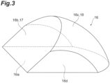
- the prism 16 includes a bottom surface 16a, a light incident surface 16b, a light reflecting surface 16c, and a pair of side surfaces 16d.
- the material of the prism 16 is, for example, acrylic resin, glass, or the like.
- the bottom surface 16a is a surface bonded to the outer surface 3b of the light transmitting substrate 3.
- the bottom surface 16a and the outer surface 3b of the light transmitting substrate 3 may be adhered to each other by an optical adhesive.
- the bottom surface 16a and the outer surface 3b of the light transmitting substrate 3 may be joined together by an optical contact.
- the bottom surface 16a is formed in a flat shape (flat surface).
- the bottom surface 16a is formed in a substantially rectangular shape.
- a light incident surface 16b is connected to one end of the bottom surface 16a in the longitudinal direction (X-axis direction).
- a light reflecting surface 16c is connected to the other end of the bottom surface 16a in the longitudinal direction.
- the side surfaces 16d are connected to each of both ends of the bottom surface 16a in the lateral direction (Y-axis direction).
- the longitudinal length of the bottom surface 16a is approximately equal to a diameter of the light transmitting substrate 3. As shown in FIG. 2 , when viewed from the direction perpendicular to the bottom surface 16a (Z-axis direction), the positions of both ends of the bottom surface 16a in the longitudinal direction coincide with the positions of the edges of the light transmitting substrate 3. Since one end of the bottom surface 16a in the longitudinal direction (i.e., the end connected to the light incident surface 16b) is not located inside the edge of the light transmitting substrate 3, the light incident surface 16b and the inner surface 32c of the ceiling wall 32 of the casing 31 can be brought into contact with each other when the electron tube 1A is disposed in the casing 31 of the electron tube module 30 described later (see FIG. 8 ).
- the end portion of the bottom surface 16a connected to the light incident surface 16b may be located inside the edge portion of the light transmitting substrate 3.
- one end of the bottom surface 16a in the longitudinal direction has a rectangular corner portion.
- the other end in the longitudinal direction of the bottom surface 16a is formed in an arc shape along the edge portion of the light transmitting substrate 3 because the light reflecting surface 16c connected to the other end has a curved surface shape.
- the light incident surface 16b is a surface to which the detection target light L (see FIG. 4 ) is incident.
- the light incident surface 16b is formed in a flat surface. When viewed from the lateral direction (Y-axis direction) of the bottom surface 16a, the light incident surface 16b is inclined with respect to the bottom surface 16a. The angle between the bottom surface 16a and the light incident surface 16b is an acute angle. In the present embodiment, the entire light incident surface 16b constitutes a light incident portion to which the detection target light L is incident.
- An antireflection film 17 is provided on the light incident surface 16b.
- the antireflection film 17 may be a single-layer film or a multilayer film.
- the antireflection film 17 may be formed by MgF 2 or the like, for example.
- the antireflection film 17 may be formed of, for example, TiO 2 , Ta 2 O 5 , SiO 2 , Al 2 O 3 , MgF 2 , or the like.
- a film forming method of the antireflection film 17 for example, a technique such as vacuum deposition or sputtering may be used.
- the light reflecting surface 16c functions as a reflecting portion that further reflects light, which is incident to the photocathode 8 through the prism 16 and the light transmitting substrate 3 and reflected by the interface between the photocathode 8 and the vacuum space S, thereby allowing the light to be incident to the photocathode 8 again.
- the light reflecting surface 16c is formed in an outwardly convex curved surface shape.
- the light reflecting surface 16c is formed in a dome shape (a curved surface shape such as a spherical surface shape or a parabolic surface shape).
- the virtual line in FIG. 1 indicates an imaginary spherical surface P along the light reflecting surface 16c.
- the virtual spherical surface P is a spherical surface approximated to the light reflecting surface 16c, and does not need to completely overlap with the light reflecting surface 16c.
- the light incident surface 16b is located inside the imaginary spherical surface P.
- the light incident surface 16b is not smoothly continuous with the light reflecting surface 16c. That is, the light incident surface 16b is located further inward than if the light incident surface were configured as a smooth continuous surface with the light reflecting surface 16c.
- the light reflecting surface 16c is provided with a reflection film 18 for improving reflectivity of light.
- the reflection film 18 may be formed of, for example, aluminum, an aluminum-based alloy, silver, a silver-based alloy, gold, or a dielectric multilayer film.
- a pair of side surfaces 16d is provided between the light incident surface 16b, the light reflecting surface 16c, and the bottom surface 16a.
- the pair of side surfaces 16d faces each other across the light incident surface 16b and the light reflecting surface 16c when viewed from the direction (Z-axis direction) facing the bottom surface 16a. More particularly, one side surface 16d is provided so as to connect one end portion of the light incident surface 16b in the Y-axis direction, one end portion of the light reflecting surface 16c in the Y-axis direction, and one end portion of the bottom surface 16a in the Y-axis direction.
- the other side surface 16d is provided so as to connect the other ends of the light incident surface 16b and the light reflecting surface 16c in the Y-axis direction and the other end of the bottom surface 16a in the Y-axis direction.
- Each side surface 16d is a surface intersecting the Y-axis direction. In the present embodiment, each side surface 16d is orthogonal to the Y-axis direction and extends along the XZ plane.
- Such a pair of side surfaces 16d functions as surfaces for supporting (holding) the prism 16. In addition, positioning of the center of the prism 16 is facilitated by the pair of side surfaces 16d.
- the pair of side surfaces 16d may be used as surfaces for fixing the electron tube 1A (prism 16) to a casing when modularizing the electron tube 1A.
- the operator can hold the prism 16 by holding the pair of side surfaces 16d. Accordingly, for example, it is possible to improve workability when the prism 16 is attached to the light transmitting substrate 3.
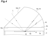
- FIG. 4 schematically illustrates a part of the side tube 2, the light transmitting substrate 3, the photocathode 8, and the prism 16 among the components of the electron tube 1A.
- the detection target light L is light directed to the light incident surface 16b of the prism 16.
- the detection target light L may be parallel light or non-parallel light.
- the detection target light L is light (non-parallel light) collected by a lens or the like (not shown) so as to have a focal point substantially at the center of the photocathode 8.
- the detection target light L enters the photocathode 8 through the prism 16 and the light transmitting substrate 3.
- the electron tube 1A is disposed with respect to the optical axis of the detection target light L such that a part or all of the detection target light L is totally reflected at the interface between the inner surface 8a on the vacuum space S side of the photocathode 8 and the vacuum space S (i.e., such that equation (3) described later is satisfied).
- the detection target light L is totally reflected at the interface between the inner surface 8a of the photocathode 8 and the vacuum space S, and travels toward the light reflecting surface 16c of the prism 16.
- the detection target light L is reflected by the light reflecting surface 16c of the prism 16 provided with the reflection film 18, and is directed to the photocathode 8 again.
- the radius of curvature of the light reflecting surface 16c may be set in accordance with an assumed angle of incident light (light incident to the light incident surface 16b) or the like. That is, the radius of curvature of the light reflecting surface 16c may be optimized such that the incident efficiency (incident amount) of the light reflected by the light reflecting surface 16c to the photocathode 8 is maximized.
- the curvature, position, size, and the like of the light reflecting surface 16c may be designed in accordance with the convergence angle or divergence angle of the light incident to the light incident surface 16b, or the incident light diameters on the photocathode 8.
- the refractive index of the prism 16 is set to n 1 (> 1)
- the refractive index of the light transmitting substrate 3 is set to n 2 (> 1)
- the refractive index of the photocathode 8 is set to n 3 (> 1).
- the refractive index of the vacuum space S is 1.
- the incident angle of the detection target light L incident from the prism 16 to the light transmitting substrate 3 is set to ⁇ 1
- the incident angle of the detection target light L incident from the light transmitting substrate 3 to the photocathode 8 is set to ⁇ 2
- the incident angle of the detection target light L incident from the photocathode 8 to the vacuum space S is set to ⁇ 3
- the critical angle of the detection target light L incident from the photocathode 8 to the vacuum space S (a minimum incident angle in which a total reflection occurs at the interface between the photocathode 8 and the vacuum space S) is set to ⁇ 0 . In this case, the following equations (1) and (2) are established.
- the electron tube 1A may be disposed with respect to the optical axis of the detection target light L so that ⁇ 3 determined based on the incident angle ⁇ 1 with respect to the light transmitting substrate 3 of the detection target light L satisfies the following equation (3). Note that it is not always necessary that all components of the detection target light L satisfy the following expression (3).
- light incident from the light incident portion (in the present embodiment, light incident surface 16b) of the prism 16 and reflected by the interface between the photocathode 8 and the vacuum space S may be further reflected by the light reflecting surface 16c of the prism 16 and may be incident to the photocathode 8 again.
- the absorption amount of the detection target light L in the photocathode 8 can be increased.
- the light reflecting surface 16c has an outwardly convex curved surface shape, it is possible to suitably return the light, which is directed from the photocathode 8 toward the light reflecting surface 16c, to the photocathode 8.
- the light incident portion (light incident surface 16b) of the prism 16 is located inward of the imaginary spherical surface P along the light reflecting surface 16c, the light source can be brought closer to the photocathode 8 than in the case where the prism 16 is formed in a hemispherical shape (that is, the light incident portion is formed by the surface of a prism having a semi-spherical surface shape).
- the detection target light L is divergent light, it is possible to suppress the detection target light L from excessively spreading from the light incident surface 16b to the photocathode 8, and to suitably cause the detection target light L (including light reflected by the light reflecting surface 16c) to be incident to the photocathode 8.
- the detection target light L is convergent light, it is easy to adjust the focus of the detection target light L to the vicinity of the photocathode 8. As described above, according to the electron tube 1A, the quantum efficiency of the photocathode 8 can be effectively improved.
- the light incident portion (light incident surface 16b) is formed in a flat shape (flat surface).
- the prism 16 can be produced relatively easily by linearly cutting a hemispherical prism member, for example.
- the electron tube module 30 described later it is possible to easily perform positioning of the electron tube 1A.
- the light incident portion is constituted by an entirety of the light incident surface 16b.
- the light incident surface 16b can be configured as a uniform surface (a flat surface in the present embodiment), the configuration of the light incident surface 16b can be simplified. That is, since it is not necessary to process a special region for allowing light to be incident on a part of the light incident surface 16b, it is possible to easily process the light incident surface 16b.
- the light incident surface 16b is provided with the antireflection film 17.
- the antireflection film 17 can effectively reduce the reflection loss of the detection target light L in the light incident surface 16b. That is, it is possible to reduce the ratio of the light reflected on the light incident surface 16b without being transmitted through the prism 16 in the detection target light L.
- the absorption amount of the detection target light L in the photocathode 8 can be increased, and the quantum efficiency of the photocathode 8 can be effectively improved.
- the light reflecting surface 16c is provided with the reflection film 18.
- the reflection film 18 can reduce a transmission loss of light in the light reflecting surface 16c (components transmitted from the light reflecting surface 16c to the outside). As a result, it is possible to suppress a decrease in the amount of light reflected by the light reflecting surface 16c and incident to the photocathode 8 again, and thus it is possible to effectively improve the quantum efficiency of the photocathode 8.
- the electron tube 1A includes the electron multiplying unit 9 provided in the vacuum container 7 to multiply the photoelectrons emitted from the photocathode 8. Accordingly, even in a case where the detection target light L is weak light (for example, fluorescence, Raman scattering light, or the like which are secondarily generated by irradiating the measurement target sample with excitation light), it is possible to suitably detect electrons corresponding to the detection target light L in the anode 10.
- the detection target light L is weak light (for example, fluorescence, Raman scattering light, or the like which are secondarily generated by irradiating the measurement target sample with excitation light)
- the electron tube 1B of the second embodiment has a configuration different from that of the electron tube 1A in the structure for multiplying photoelectrons emitted from the photocathode 8 (that is, a structure inside the vacuum container).
- the configurations of the light transmitting substrate 3, the photocathode 8, the prism 16, the antireflection film 17, and the reflection film 18 are the same as those of the electron tube 1A.
- the electron tube 1B is a so-called electron-bombarded multiplication type photo-detector (hybrid photo-detector (HPD)) which accelerates photoelectrons emitted from the photocathode 8 in response to the incidence of light and obtains a high gain in the semiconductor element so that weak light can be detected.
- HPD hybrid photo-detector
- the electron tube 1B includes a vacuum container 20 of which an inside is maintained in a vacuum state.
- the vacuum container 20 includes the light transmitting substrate 3, a cylindrical cathode electrode 21, a cylindrical side plate 22 which is formed of an insulation material such as ceramic, an annular intermediate electrode 23a which is fixed so as to be sandwiched between a first side plate 22a and a second side plate 22b formed by dividing the side plate 22 into four parts, an annular intermediate electrode 23b which is fixed so as to be sandwiched between the second side plate 22b and a third side plate 22c, an annular intermediate electrode 23c which is fixed so as to be sandwiched between the third side plate 22c and a fourth side plate 22d, a metal flange 24, and a disk-shaped stem 25 which is airtightly connected to the metal flange 24.
- the light transmitting substrate 3, the cathode electrode 21, the side plate 22, the intermediate electrode 23, the metal flange 24, and the stem 25 are stacked and arranged
- the side plate 22 is provided between the cathode electrode 21 and the metal flange 24.
- One end of the side plate 22 is airtightly bonded to the end surface of the cathode electrode 21 by brazing or the like.
- the other end of the side plate 22 is airtightly bonded to the metal flange 24 provided in the outer periphery of the stem 25 by brazing or the like.
- the intermediate electrodes 23a, 23b, and 23c are formed in a ring shape having an opening portion centered on the central axis AX of the vacuum container 20 and are arranged electrically independently from the photocathode 8 at a predetermined interval along the inner wall of the side plate 22.
- the outer diameters of the cathode electrode 21, the side plate 22, and the cylindrical portions of the metal flange 24 are substantially the same and the inner diameter of the cathode electrode 21 is smaller than the inner diameter of the side plate 22.
- the inner wall surface of the cathode electrode 21 is located inside in relation to the inner wall surface of the side plate 22 from one end to the other end of the cathode electrode 21 along the central axis AX.
- the inner diameters of the opening portions of the intermediate electrodes 23a, 23b, and 23c are made as small as possible within a range that does not interfere with the electron trajectory, that is, a range that does not become extremely small compared to the diameter of the photocathode 8 and the intermediate electrodes 23a, 23b, and 23c protrude inward in relation to the cathode electrode 21 from the inner wall surface of the cylindrical side plate 22. Accordingly, the charging of the side plate 22 by stray electrons when controlling the trajectory of electrons emitted from the photocathode 8 and the influence on the electron trajectory due to the charging can be eliminated.
- the intermediate electrodes 23a, 23b, and 23c are fixed by brazing or the like while being sandwiched between the side plates 22 so as to be integrated with the side plates 22.
- a ring-shaped rising electrode 26 is fixed to the side of the central axis AX of the metal flange 24 of the vacuum container 20.
- the rising electrode 26 has an opening of a diameter smaller than those of the intermediate electrodes 23a, 23b, and 23c while being disposed concentrically with the metal flange 24.
- the opening forms a substantially columnar front end portion 26a extending along the inner wall of the side plate 22 toward the light transmitting substrate 3.
- a semiconductor element 27 (electron detector) including avalanche photodiode (APD) is fixed onto a surface on the side of the vacuum space S in the stem 25 so as to face the photocathode 8.
- the APD is a semiconductor element which bonds a P region and an N region of a high concentration and forms an electric field high enough for avalanche amplification.
- the semiconductor element 27 multiplies the photoelectrons to be converted into an electrical signal and outputs the signal to the outside through a pin 28 provided through the stem 25.
- the semiconductor element 27 having a function of multiplying photoelectrons serves as an electron detector. According to the above-described configuration, it is possible to appropriately detect electrons in response to the detection target light in the semiconductor element 27 even when the detection target light is weak light. Further, in the electron tube 1B, since the semiconductor element 27 serving as the electron detector has an electron multiplying function, there is no need to provide the electron multiplying unit 9 in the electron tube 1A of the first embodiment. Furthermore, a detailed structure of the electron tube 1B is not limited to the above-described example. For example, a part of the intermediate electrode 23 may be omitted and the rising electrode 26 may be omitted.
- the electron tube module 30 includes an electron tube 1A and a casing 31 that accommodates the electron tube 1A.
- the casing 31 is formed in a substantially rectangular parallelepiped shape.
- the casing 31 is formed of, for example, metal or resin.
- the casing 31 has a ceiling wall 32 (wall portion), a bottom wall 33, and a side wall 34.
- the ceiling wall 32 and the bottom wall 33 face each other in a direction along the central axis AX1 of the casing 31.
- the ceiling wall 32 and the bottom wall 33 are formed in rectangular plate shapes having the same size as viewed from the direction along the central axis AX1.
- the side wall 34 is formed in a square tubular shape extending along the central axis AX1, and connects an edge portion of the ceiling wall 32 and an edge portion of the bottom wall 33.
- a circuit board 41 for supplying a voltage to the electron tube 1A via the stem pin 5, and a booster circuit 42 connected to the circuit board 41 and generating a high voltage to be supplied to the electron tube 1A are housed in the casing 31 together with the electron tube 1A.
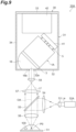
- the electron tube 1A is disposed and fixed in the casing 31 such that a central axis AX2 (an axial line parallel to the Z-axis in FIG. 1 ) of the electron tube 1A is inclined with respect to the central axis AX1 of the casing 31.
- An opening 32a for guiding the detection target light to the electron tube 1A in the casing 31 is formed in the ceiling wall 32.
- the opening 32a extends from the outer surface 32b to the inner surface 32c of the ceiling wall 32.
- the opening 32a is formed in a circular shape when viewed from a direction along the central axis AX1.
- the electron tube 1A is arranged in the casing 31 so that the light introduced from the opening 32a enters the light incident surface 16b.
- the electron tube 1A is disposed in the casing 31 such that the light incident surface 16b of the prism 16 is parallel to the ceiling wall 32 and at least a portion of the light incident surface 16b of the prism 16 is exposed to the outside through the opening 32a.
- the light incident surface 16b of the prism 16 abuts the inner surface 32c of the ceiling wall 32. Accordingly, it is possible to easily and accurately position the electron tube 1A in the casing 31 such that the light incident surface 16b and the ceiling wall 32 (inner surface 32c) are parallel to each other.
- the edge of the light transmitting substrate 3 interferes with the ceiling wall 32, so that a gap is formed between the light incident surface 16b and the inner surface 32c of the ceiling wall 32.
- a spacer member for filling the gap may be disposed between the inner surface 32c of the ceiling wall 32 and the light incident surface 16b.
- the inner surface 32c of the ceiling wall 32 and the light incident surface 16b may be brought into contact with each other by making the ceiling wall 32 thicker in a portion corresponding to the gap than in other portions.
- the light incident surface 16b of the prism 16 is joined to the inner surface 32c of the ceiling wall 32.
- the light incident surface 16b and the inner surface 32c may be joined by, for example, an adhesive.
- an adhesive for example, a glass bonding adhesive such as a silicone-based adhesive may be used.
- a primer suitable for the material of the inner surface 32c may be applied to the inner surface 32c in advance. In this case, after the primer coated on the inner surface 32c is dried, the inner surface 32c coated with the primer and the light incident surface 16b are bonded to each other by the glass bonding adhesive.
- an adhesive having good compatibility with the material of the inner surface 32c may be used as the adhesive.
- a primer for glass may be applied to the light incident surface 16b in advance.
- the entire portion of the light incident surface 16b that comes into contact with the inner surface 32c may be bonded to the inner surface 32c, or a portion of the light incident surface 16b that comes into contact with the inner surface 32c may be bonded to the inner surface 32c.
- the light incident surface 16b does not necessarily need to be joined to the inner surface 32c of the ceiling wall 32, and the electron tube 1A may be fixed to the casing 31 in a portion other than the light incident surface 16b.
- the electron tube module 30 described above includes the electron tube 1A, an effect similar to that of the electron tube 1A described above is obtained.
- the electron tube 1A can be appropriately protected.
- the light incident surface 16b formed in a flat shape is disposed so as to be parallel to the ceiling wall 32, positioning of the electron tube 1A in the casing 31 is facilitated. For example, by bringing the light incident surface 16b into contact with the inner surface 32c of the ceiling wall 32 as described above, it is possible to easily position the electron tube 1A.
- the electron tube module 30 by adjusting the position of the electron tube module 30 so that the ceiling wall 32 is orthogonal to the optical axis of the detection target light, it is possible to easily and appropriately arrange the electron tube module 30.
- the central axis AX1 of the casing 31 and the optical axis of the detection target light are parallel to each other, it is possible to arrange the electron tube module 30 in a natural orientation in a well-fitting manner in an optical system including the electron tube module 30 (optical device 50A to 50C described later or the like).
- the optical devices 50A to 50C including the electron tube (here, as an example, the electron tube module 30 including the electron tube 1A) will be described with reference to FIGS. 9 to 11 .
- an optical device 50A is a two-photon laser microscope (two-photon excitation microscope or two-photon microscope) which irradiates a sample 100 placed on a sample stage 51 with excitation light Le and detects weak fluorescence Lf generated from the sample 100 at a focal position P0 of an objective lens 56.
- the optical device 50A includes the sample stage 51, a laser irradiation unit 52A (light source), a condenser lens 53, a collimator lens 54, a dichroic mirror 55, an objective lens 56, a condenser lens 57, a collimator lens 58, and the electron tube module 30 detecting the fluorescence Lf.
- the collimator lens 58 may be omitted.
- the sample stage 51 is a portion on which the sample 100 of the measurement target is placed.
- the sample stage 51 is, for example, a movable stage.
- the sample 100 is, for example, a biological sample and emits the fluorescence Lf by being irradiated with the excitation light Le.
- the laser irradiation unit 52A is a light source which outputs the excitation light Le (light) irradiating the sample 100 of the measurement target.
- the excitation light Le output by the laser irradiation unit 52A is near-infrared ultrashort pulse laser light. In this embodiment, as an example, the excitation light Le output by the laser irradiation unit 52A is parallel light.
- the condenser lens 53 is disposed on the optical path of the excitation light Le output from the laser irradiation unit 52A and converts the excitation light Le into a point light source by condensing the excitation light Le.
- the collimator lens 54 is disposed at the rear stage in relation to the condenser lens 53 and parallelizes (collimates) the excitation light Le.
- the dichroic mirror 55 is a mirror member formed so that the excitation light Le is reflected and the fluorescence Lf is transmitted and is disposed at the rear stage of the collimator lens 54.
- the excitation light Le which becomes parallel light by the collimator lens 54 is reflected at the dichroic mirror 55, passes through the objective lens 56, and reaches the sample 100. Accordingly, two-photon excitation is generated only at the focal position P0 of the objective lens 56 and the fluorescence Lf is generated from the sample 100 at the focal position P0.
- the fluorescence Lf generated in the sample 100 follows a path opposite to the excitation light Le, passes through the objective lens 56, and is transmitted through the dichroic mirror 55. Then, the fluorescence Lf is condensed by the condenser lens 57.
- the fluorescence Lf condensed by the condenser lens 57 is parallelized by the collimator lens 58 disposed behind the condensing point of the condenser lens 57.
- the electron tube module 30 is disposed at the rear stage of the collimator lens 58 so that the optical axis OA of the fluorescence Lf generated in the sample 100 is orthogonal to the light incident surface 16b of the prism 16.
- the fluorescence Lf is parallelized by the collimator lens 58 so as to enter the opening 32a of the ceiling wall 32.
- the fluorescence Lf which is parallelized in this way is incident to the light incident surface 16b of the prism 16 through the opening 32a and is detected by the electron tube module 30.
- the optical device 50A has the same effect as that of the electron tube module 30 by including the electron tube module 30 as a detector which detects the detection target light (here, fluorescence Lf). That is, it is possible to effectively improve the quantum efficiency of the photocathode 8 in the electron tube 1A by using the prism 16. As a result, it is possible to appropriately detect electrons in response to the fluorescence Lf in the anode 10 of the electron tube 1A. Further, as illustrated in FIG. 9 , since the electron tube 1A is accommodated in the casing 31, the electron tube module 30 can be disposed in an accommodation state so that the central axis AX1 (see FIG. 8 ) of the casing 31 is parallel to the optical axis OA of the detection target light (the fluorescence Lf) in the optical device 50A.
- the electron tube 1A may be configured so that a part or all of the fluorescence Lf (the detection target light) incident to the photocathode 8 through the prism 16 and the light transmitting substrate 3 is totally reflected at the interface between the photocathode 8 and the vacuum space S.
- the electron tube 1A may be configured and disposed in the optical device 50A so that the above-described equation (3) is established for the fluorescence Lf as the detection target light L in FIG. 5 .
- an optical device 50B is a confocal laser microscope which irradiates the sample 100 (measurement target) placed on the sample stage 51 with the excitation light Le and detects weak fluorescence Lf1 generated from the sample 100 at the focal position P0 of the objective lens 56.
- the optical device 50B is different from the optical device 50A in that a laser irradiation unit 52B is provided instead of the laser irradiation unit 52A and a pin hole 59 is further provided and the other configurations are the same as those of the optical device 50A.
- the excitation light Le output by the laser irradiation unit 52B is a visible ultraviolet laser.
- fluorescence is generated from an irradiation region including a region other than the focal position P0 of the objective lens 56.
- the fluorescence Lf1 indicates the fluorescence generated at the focal position P0
- the fluorescence Lf2 indicates the fluorescence generated at a position (here, as an example, in the vicinity of the contact position between the sample 100 and the sample stage 51) other than the focal position P0.
- the pin hole 59 through which only the fluorescence Lf1 generated from the focal position P0 passes is provided at the rear stage of the condenser lens 57. Accordingly, only the fluorescence Lf1 passes through the pin hole 59 and is guided to the incident surface (the light incident surface 16b of the prism 16) of the electron tube module 30 through the collimator lens 58. That is, the pin hole 59 shields the fluorescence Lf2 generated in a region other than the focal position P0. Also in the optical device 50B, the same effect as that of the optical device 50A is obtained.
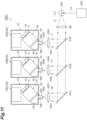
- an optical device 50C is a device (flow cytometer) that performs flow cytometry.
- the optical device 50C includes a laser irradiation unit 52C, a flow cell FC, a collimator lens 60, a plurality of (here, as an example, three) dichroic mirrors 61A, 61B, and 61C, a plurality of condenser lenses 62A, 62B, and 62C, a plurality of collimator lenses 63A, 63B, and 63C, and a plurality of electron tube modules 30A, 30B, and 30C.
- the collimator lenses 63A, 63B, and 63C may be omitted.
- the flow cell FC is a device that distributes a sample solution including the sample 100 such as a plurality of cells to be measured.
- the flow cell FC has a function of aligning the sample 100 in the sample solution so that the samples 100 sequentially flow one by one.
- the laser irradiation unit 52C is configured to irradiate a predetermined irradiation position of the flow cell FC with the excitation light Le (here, as an example, a 488 nm argon laser). Accordingly, each of the samples 100 flowing through the flow cell FC and passing through the irradiation position is sequentially irradiated with the excitation light Le. When the sample 100 is irradiated with the excitation light Le in this way, the fluorescence Lf is generated in the sample 100.
- the collimator lens 60 parallelizes the fluorescence Lf generated in the sample 100.
- the dichroic mirrors 61A, 61B, and 61C are disposed in this order at the rear stage of the collimator lens 60.
- the dichroic mirror 61A of the first stage is configured to reflect the red light Lr and transmit light having a shorter wavelength than the red light Lr.
- the dichroic mirror 61B of the second stage disposed at the rear stage of the dichroic mirror 61A is configured to reflect the yellow light Ly in the light transmitted through the dichroic mirror 61A and transmit light having a shorter wavelength than the yellow light Ly.
- the dichroic mirror 61C of the third stage disposed at the rear stage of the dichroic mirror 61B is configured to reflect the green light Lg in the light transmitted through the dichroic mirror 61B and transmit light having a shorter wavelength than the green light Lg.
- the condenser lens 62A, the collimator lens 63A, and the electron tube module 30A are disposed on the optical path of the red light Lr reflected by the dichroic mirror 61A. That is, the dichroic mirror 61A, the condenser lens 62A, the collimator lens 63A, and the electron tube module 30A constitute an optical system that detects the red light Lr included in the fluorescence Lf.
- the electron tube module 30A is disposed at the rear stage of the collimator lens 63A so that the optical axis OA1 of the red light Lr reflected by the dichroic mirror 61A is orthogonal to the light incident surface 16b of the prism 16.
- the red light Lr is parallelized by the condenser lens 62A and the collimator lens 63A so as to enter the opening 32a of the ceiling wall 32.
- the red light Lr parallelized in this way is incident to the light incident surface 16b of the prism 16 through the opening 32a and is detected by the electron tube module 30A.
- the condenser lens 62B, the collimator lens 63B, and the electron tube module 30B are disposed on the optical path of the yellow light Ly reflected by the dichroic mirror 61B. That is, the dichroic mirror 61B, the condenser lens 62B, the collimator lens 63B, and the electron tube module 30B constitute an optical system that detects the yellow light Ly included in the fluorescence Lf.
- the electron tube module 30B is disposed at the rear stage of the collimator lens 63B so that the optical axis OA2 of the yellow light Ly reflected by the dichroic mirror 61B is orthogonal to the light incident surface 16b of the prism 16.
- the yellow light Ly is parallelized by the condenser lens 62B and the collimator lens 63B so as to enter the opening 32a of the ceiling wall 32.
- the yellow light Ly parallelized in this way is incident to the light incident surface 16b of the prism 16 through the opening 32a and is detected by the electron tube module 30B.
- the condenser lens 62C, the collimator lens 63C, and the electron tube module 30C are disposed on the optical path of the green light Lg reflected by the dichroic mirror 61C. That is, the dichroic mirror 61C, the condenser lens 62C, the collimator lens 63C, and the electron tube module 30C constitute an optical system that detects the green light Lg included in the fluorescence Lf.
- the electron tube module 30C is disposed at the rear stage of the collimator lens 63C so that the optical axis OA3 of the green light Lg reflected by the dichroic mirror 61C is orthogonal to the light incident surface 16b of the prism 16.
- the green light Lg is parallelized by the condenser lens 62C and the collimator lens 63C so as to enter the opening 32a of the ceiling wall 32.
- the green light Lg which is parallelized in this way is incident to the light incident surface 16b of the prism 16 through the opening 32a and is detected by the electron tube module 30C.
- optical devices 50A, 50B, and 50C have been described above as examples of an optical device including an electron tube (here, an electron tube module), the configuration of the optical device is not limited to the above.
- an electron tube 1A that is not housed in the casing 31 may be provided instead of the electron tube module 30 as a portion that detects the detection target light.
- the electron tube 1A, 1B, or the electron tube module 30 may be incorporated into an optical device other than the optical devices 50A, 50B, and 50C exemplified in the present disclosure.
- the electron tube 1A, 1B, or the electron tube module 30 may be used for applications other than the two photon laser microscope, the confocal laser microscope, and the flow cytometer.
- the detection target light may be guided to a light incident portion (light incident surface 16b) of the prism 16 via a light guide body such as an optical fiber, for example, without using an optical system as in the examples of FIGS. 9 to 11 .
- the present disclosure is not limited to the above-described embodiment.
- the material and shape of each component are not limited to those described above, and various materials and shapes may be employed.
- the shape of the prism is not limited to the prism 16 of the above-described embodiment. Some modifications of the prism will be described below.
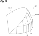
- FIG. 12 is a perspective view showing a prism 16A according to a first modification.
- the curved surface shape of the light reflecting surface 16c is a curved surface shape configured in a pseudo manner by a plurality of plane portions 19. More particularly, the light reflecting surface 16c is formed by a plurality of plane portions 19. That is, the light reflecting surface 16c is formed by connecting a plurality of plane portions 19 to each other. In this case, since the light reflecting surface 16c can be formed only by a process of linearly cutting the prism member, the process becomes easy.
- the number of plane portions 19 constituting the light reflecting surface 16c, and the shape and size of each plane portion 19 are not limited to a specific form. By reducing the size of each plane portion 19 and increasing the number of plane portions 19 constituting the light reflecting surface 16c, a curved surface shape with a high degree of approximation can be obtained.
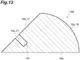
- FIG. 13 is a cross-sectional view illustrating a prism 16B according to a second modification.
- the prism 16B differs from the prism 16 in that a concave portion 16e opening to a portion of the light incident surface 16b is formed.
- the concave portion 16e is, for example, a non-through hole having a cylindrical cross section.
- a light guide such as an optical fiber
- the front end portion of the optical fiber is inserted into the concave portion 16e, so that the distance between the light source and the photocathode 8 can be further reduced.
- the light incident portion is constituted by the concave portion 16e. More particularly, the bottom surface 16f of the concave portion 16e functions as the light incident portion to which light is incident.
- the antireflection film 17 is provided on the entire light incident surface 16b in the prism 16B, the antireflection film 17 may be provided on only the bottom surface 16f (light incident portion) of the concave portion 16e in a case where light is incident to only the bottom surface 16f as described above.
- the bottom surface 16f is formed in a flat shape (flat surface), but the bottom surface 16f may be formed in an inwardly convex curved surface shape or an outwardly convex curved surface shape.
- the light source here, the front end portion of the optical fiber
- the light source is caused to enter the concave portion 16e, and thus the light source can be brought closer to the photocathode 8.
- FIG. 14 is a cross-sectional view showing a prism 16C according to a third modification.
- the prism 16c differs from the prism 16B in that the light incident surface 16b has a curved surface shape that is continuous with the light reflecting surface 16c. That is, the prism 16C is obtained by forming the concave portion 16e on a part of the light incident surface 16b of a hemispherical prism. With such a configuration, the same effect as that of the prism 16B can be obtained.
- FIG. 15 is a cross-sectional view showing a prism 16D according to a fourth modification.
- the prism 16D differs from the prism 16 in that the light incident surface 16b is not a flat surface but has an inwardly convex curved surface shape. According to such a prism 16D, by bringing the light source close to the light incident surface 16b, the interval between the light source and the photocathode 8 can be made shorter than that in the case of using the prism 16.
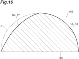
- FIG. 16 is a cross-sectional view showing a prism 16E according to a fifth modification.
- the prism 16E differs from the prism 16 in that the light incident surface 16b is not a flat surface but has an outwardly convex curved surface shape. Note that the radius of curvature of the light incident surface 16b is set within a range that falls inside the imaginary spherical surface P. According to such a prism 16E, for example, in a case where the detection target light incident to the light incident surface 16b is parallel light, it is possible to condense the parallel light toward a substantially central position of the photocathode 8.
- an electron tube 1A or 1B (that is, a photomultiplier tube or an HPD) including an electron multiplication function (the electron multiplying unit 9 in the first embodiment or the semiconductor element 27 in the second embodiment) has been illustrated, but such an electron multiplication function is not essential in the electron tube.
- the electron tubes 1A and 1B may be configured as a photoelectric tube (photoelectric conversion tube) including the photocathode 8 and an anode that directly detects photoelectrons emitted from the photocathode 8 in the vacuum container.
- 1A, 1B electron tube 3 light transmitting substrate; 3a inner surface; 3b outer surface; 7, 20 vacuum container; 8 photocathode; 9 electron multiplying unit; 10 anode (electron detector); 16 prism; 16a bottom surface; 16b light incident surface (light incident portion); 16c.
Landscapes
- Physics & Mathematics (AREA)
- General Physics & Mathematics (AREA)
- Optics & Photonics (AREA)
- Analytical Chemistry (AREA)
- Chemical & Material Sciences (AREA)
- Health & Medical Sciences (AREA)
- General Health & Medical Sciences (AREA)
- Pathology (AREA)
- Immunology (AREA)
- Nuclear Medicine, Radiotherapy & Molecular Imaging (AREA)
- Life Sciences & Earth Sciences (AREA)
- Biochemistry (AREA)
- Engineering & Computer Science (AREA)
- General Engineering & Computer Science (AREA)
- Computer Vision & Pattern Recognition (AREA)
- Electron Tubes For Measurement (AREA)
- Photometry And Measurement Of Optical Pulse Characteristics (AREA)
- Common Detailed Techniques For Electron Tubes Or Discharge Tubes (AREA)
- Microscoopes, Condenser (AREA)
- Surface Treatment Of Optical Elements (AREA)
- Investigating, Analyzing Materials By Fluorescence Or Luminescence (AREA)
- Optical Elements Other Than Lenses (AREA)
- Measurement Of Radiation (AREA)
Abstract
Description
- The present disclosure relates to an electron tube, an electron tube module, and an optical device.
- Conventionally, an electron tube such as a photomultiplier tube for detecting weak light such as fluorescence generated from a sample has been known. The electron tube includes a vacuum container having a light transmitting substrate and a photocathode provided on an inner surface of the vacuum side of the light transmitting substrate. Non-Patent
Document 1 discloses a configuration in which a prism having a semi-spherical surface shape is provided on the outer surface of the light transmitting substrate. In this configuration, light incident to the light incident surface of the prism is reflected at the interface between the photocathode and the vacuum space, and then further reflected at a light reflecting surface opposite to the light incident surface of the prism back to the photocathode. Thus, the quantum efficiency (QE) of the photocathode is improved. - [Non-Patent Document 1] J. B. Oke and Rudolph E. Schild. A Practical Multiple Reflection Technique for Improving the Quantum Efficiency of Photomultiplier Tubes. APPLIED OPTICS Vol.7. No.4 617-622 (1968)
- However, in the configuration disclosed in
Non-Patent Document 1, the light incident surface of the prism is along the semi-spherical surface, and the distance between the light incident surface of the prism and the photocathode is relatively large. Therefore, the light source of the detection target light may not be sufficiently close to the photocathode. For example, when the prism has a hemispherical shape, the distance from the light incident surface of the prism to the photocathode is large. Therefore, when the detection target light is divergent light, it is assumed that the detection target light (primary light) does not fit into the photocathode. When the prism has a hemispherical shape, it is difficult for light reflected at a location other than the center of the photocathode (the center of a sphere corresponding to the prism shape) to return to the photocathode again via the light reflecting surface. For this reason, when the detection target light is convergent light, it is preferable to focus the detection target light on the photocathode from the viewpoint of obtaining good quantum efficiency. However, it may be difficult to adjust the focal position as described above because the light source cannot be sufficiently close to the photocathode. Therefore, the configuration disclosed in Non-PatentDocument 1 has room for improvement from the viewpoint of improving the quantum efficiency of the photocathode. - Hence, an object of an aspect of the present disclosure is to provide an electron tube, an electron tube module, and an optical device that can effectively improve the quantum efficiency of a photocathode.
- An electron tube according to an aspect of the present disclosure includes: a vacuum container that includes a light transmitting substrate and forms a vacuum space; a photocathode provided on an inner surface of the light transmitting substrate facing the vacuum space and configured to emit photoelectrons into the vacuum space in response to light incident through the light transmitting substrate; an electron detector provided in the vacuum container and configured to detect electrons derived from the photoelectrons; and a prism bonded to an outer surface of the light transmitting substrate opposite to the inner surface thereof. The prism includes: a bottom surface bonded to the outer surface of the light transmitting substrate; a light incident surface having a light incident portion to which light is incident; and a light reflecting surface configured to further reflect light, which is incident to the light incident portion and reflected at an interface between the photocathode and the vacuum space, so that the light is incident to the photocathode again. The light reflecting surface has an outwardly convex curved surface shape, and the light incident portion is located inward of an imaginary spherical surface that is along the light reflecting surface.
- According to the electron tube, light incident from the light incident portion of the prism and reflected by the interface between the photocathode and the vacuum space may be further reflected by the light reflecting surface of the prism and re-incident to the photocathode. As a result, the absorption amount of the detection target light in the photocathode can be increased. Here, since the light reflecting surface has an outwardly convex curved surface shape, it is possible to suitably return the light, which is directed from the photocathode to the light reflecting surface, to the photocathode. Further, since the light incident portion of the prism is located inward of the imaginary spherical surface along the light reflecting surface, the light source can be closer to the photocathode than in the case where the prism is formed in a hemispherical shape (that is, the light incident portion (light incident surface) is formed by the surface of a prism having a semi-spherical surface shape). As a result, in a case where the detection target light is divergent light, it is possible to suppress the detection target light from excessively spreading from the light incident portion to the photocathode, and to suitably cause the detection target light (including light reflected by the light reflecting surface) to be incident to the photocathode. When the detection target light is convergent light, it is easy to adjust the focus of the detection target light to the vicinity of the photocathode. As described above, according to the electron tube, the quantum efficiency of the photocathode can be effectively improved.
- The photocathode may be formed in a flat plate shape along the inner surface of the light transmitting substrate. In this case, the photocathode can be easily formed by forming a film on the inner surface of the light transmitting substrate.
- The photocathode may be formed on a portion of the inner surface of the light transmitting substrate. In this case, the material cost of the photocathode can be reduced as compared with the case where the photocathode is formed on the entire inner surface of the light transmitting substrate.
- The light incident portion may be formed in a flat shape. Thus, for example, the prism can be produced relatively easily by linearly cutting a hemispherical prism member. Note that the light incident portion may have an outwardly convex curved surface shape. Alternatively, the light incident portion may have an inwardly convex curved surface shape.
- The light incident portion may be constituted by an entirety of the light incident surface. In this case, since the light incident surface may be configured as a uniform surface, the configuration of the light incident surface may be simplified.
- The light incident portion may be constituted by a concave portion opening to a portion of the light incident surface. In this case, the light source can be brought closer to the photocathode by inserting the light source of a light guide such as an optical fiber into the concave portion.
- At least the light incident portion of the light incident surface may be provided with an antireflection film. In this case, a reflection loss of the detection target light at the light incident portion (light incident surface) may be effectively reduced by the antireflection film. As a result, the absorption amount of the detection target light in the photocathode can be increased, and the quantum efficiency of the photocathode can be more effectively improved.
- The light reflecting surface may be provided with a reflection film. In this case, the reflection film can reduce a transmission loss of light on the light reflecting surface (a component that is transmitted from the light reflecting surface to the outside). Accordingly, it is possible to suppress a decrease in the amount of light reflected by the light reflecting surface and re-incident to the photocathode, and thus to more effectively improve the quantum efficiency of the photocathode.
- The prism may further include a pair of side surfaces provided between the light incident surface, the light reflecting surface, and the bottom surface, and facing each other with the light incident surface and the light reflecting surface interposed therebetween when viewed from a direction facing the bottom surface. Such a pair of side surfaces functions as surfaces for supporting (holding) the prism. For example, the operator can hold the prism by holding a pair of side surfaces. Accordingly, for example, it is possible to improve workability when the prism is attached to the light transmitting substrate.
- The electron tube may further include an electron multiplying unit provided in the vacuum container to multiply the photoelectrons. Alternatively, the electron detector may be a semiconductor element that multiplies photoelectrons. According to the above configuration, even in a case where the detection target light is weak light (for example, fluorescence, Raman scattering light, or the like which are secondarily generated by irradiating the measurement target sample with excitation light), it is possible to suitably detect electrons corresponding to the detection target light in the electron detector.
- The curved surface shape of the light reflecting surface may be a curved surface shape configured in a pseudo manner by a plurality of plane portions. In this case, since the light reflecting surface can be formed only by linearly cutting the prism member, the processing becomes easy.
- An electron tube module according to another aspect of the present disclosure includes the electron tube and a casing that accommodates the electron tube. The casing has a wall portion formed with an opening, and the electron tube is arranged in the casing so that light introduced from the opening is incident to the light incident surface.
- Since the electron tube module includes the electron tube described above, the same effect as that of the electron tube described above is obtained. Further, by accommodating the electron tube in the casing, it is possible to appropriately protect the electron tube.
- The light incident surface may be formed in a flat shape and arranged to be parallel to the wall portion. This makes it possible to easily position the electron tube in the casing.
- An optical device according to still another aspect of the present disclosure includes the electron tube and a light source that outputs light with which a measurement target is irradiated. The electron tube is disposed such that detection target light generated by irradiating the measurement target with the light is incident to the light incident surface.
- Since the optical device includes the electron tube as a detection unit that detects the detection target light, the same effect as that of the electron tube described above is obtained.
- The electron tube may be configured such that a part or all of the detection target light incident to the photocathode through the prism and the light transmitting substrate is totally reflected at an interface between the photocathode and the vacuum space. According to the above configuration, it is possible to increase the absorption amount of the detection target light in the photocathode by the detection target light returning to the photocathode again after being totally reflected, and to effectively improve the quantum efficiency of the photocathode.
- According to the present disclosure, it is possible to provide an electron tube, an electron tube module, and an optical device that can effectively improve the quantum efficiency of the photocathode.
-
-
FIG. 1 is a cross-sectional view of an electron tube according to a first embodiment. -
FIG. 2 is a plan view of the electron tube ofFIG. 1 . -
FIG. 3 is a perspective view of a prism included in the electron tube ofFIG. 1 . -
FIG. 4 is a schematic diagram showing an optical path of detection target light in the electron tube ofFIG. 1 . -
FIG. 5 is a schematic diagram for explaining conditions for total reflection of detection target light at an interface between a photocathode and a vacuum space. -
FIG. 6 is a cross-sectional view of an electron tube according to a second embodiment. -
FIG. 7 is a perspective view of an electron tube module according to an embodiment. -
FIG. 8 is a partial cross-sectional view of the electron tube module. -
FIG. 9 is a schematic configuration diagram of a first example of an optical device. -
FIG. 10 is a schematic configuration diagram of a second example of an optical device. -
FIG. 11 is a schematic configuration diagram of a third example of an optical device. -
FIG. 12 is a perspective view showing a first modification of the prism. -
FIG. 13 is a cross-sectional view showing a second modification of the prism. -
FIG. 14 is a cross-sectional view showing a third modification of the prism. -
FIG. 15 is a cross-sectional view showing a fourth modification of the prism. -
FIG. 16 is a cross-sectional view showing a fifth modification of the prism. - Hereinafter, embodiments of the present disclosure will be described with reference to the drawings. In the drawings, the same or corresponding portions are denoted by the same reference numerals, and redundant description will be omitted.
- As illustrated in
FIGS. 1 and2 , theelectron tube 1A according to the first embodiment is a photomultiplier tube having an electron multiplying function (anelectron multiplying unit 9 described later). InFIGS. 1 and2 , the Z-axis direction is an extending direction of theelectron tube 1A (that is, an extending direction of aside tube 2 described later). The Y-axis direction is a direction in which a pair ofside surfaces 16d of theprism 16 described later face each other. The X-axis direction is a direction orthogonal to the Y-axis direction and the Z-axis direction. The X-axis direction is also a direction along an optical axis (central axis) of a detection target light L described later when viewed from the Z-axis direction. - The
electron tube 1A includes ametallic side tube 2 having a substantially cylindrical shape. Alight transmitting substrate 3 having good light transmittance with respect to incident light (detection target light) is airtightly fixed to an upper end portion of theside tube 2. In the present embodiment, thelight transmitting substrate 3 is formed in a disk shape, and a peripheral edge portion of thelight transmitting substrate 3 is fixed to the upper end portion of theside tube 2. A disk-shapedstem 4 is disposed at a lower opening end of theside tube 2. A plurality of conductive stem pins 5 which are disposed in the circumferential direction at intervals are airtightly inserted into thestem 4 at the substantially circumferential positions. Eachstem pin 5 is inserted throughopenings 4a formed at the corresponding positions on the upper surface side and the lower surface side of thestem 4. Further, a metallic ring-shapedside tube 6 is airtightly fixed so as to surround thestem 4 from the lateral side. Aflange portion 2a formed at the lower end portion of theside tube 2 and aflange portion 6a formed at the upper end portion of the ring-shapedside tube 6 are welded to each other so that theside tube 2 and the ring-shapedside tube 6 are airtightly fixed to each other. In this way, avacuum container 7 of which an inside is maintained in a vacuum state is formed by theside tube 2, thelight transmitting substrate 3, and thestem 4. - A
photocathode 8, anelectron multiplying unit 9, and an anode 10 (electron detector) are provided in thevacuum container 7. Thephotocathode 8 is provided on aninner surface 3a of thelight transmitting substrate 3 facing the vacuum space S. Thephotocathode 8 may be provided directly on theinner surface 3a of thelight transmitting substrate 3, or may be provided on theinner surface 3a of thelight transmitting substrate 3 via an underlayer (for example, oxides such as manganese oxides, magnesium oxides, and titanium oxides). Thephotocathode 8 emits photoelectrons into the vacuum space S in response to light incident through thelight transmitting substrate 3. Thephotocathode 8 is a so-called transmission type photocathode, and receives light on the upper surface on thelight transmitting substrate 3 side and emits photoelectrons from the lower surface on the vacuum space S side. Thephotocathode 8 may be formed of a material such as GaAsP, GaAs, or InGaAs. Alternatively, thephotocathode 8 may be an alkaline antimonide photocathode or an alkaline telluride photocathode. - Here, from the viewpoint of increasing the absorption amount of the detection target light in the
photocathode 8, it is preferable that the thickness of thephotocathode 8 is large. On the other hand, from the viewpoint of improving the electron emission efficiency from thephotocathode 8 to the vacuum space S, it is preferable that the thickness of thephotocathode 8 is small. Theelectron tube 1A can effectively increase the absorption amount of the detection target light in thephotocathode 8 by including theprism 16 to be described later, so that thephotocathode 8 can be made thinner. In view of the above, when thephotocathode 8 is formed of GaAsP, GaAs, or InGaAs, the film thickness of thephotocathode 8 may be 3 µm or less. In the case where thephotocathode 8 is an alkaline antimonide photocathode or an alkaline telluride photocathode, the thickness of thephotocathode 8 may be 0.5 µm or less. - The
photocathode 8 is formed in a flat plate shape along theinner surface 3a of thelight transmitting substrate 3. In this case, thephotocathode 8 can be easily formed by forming a film on theinner surface 3a of thelight transmitting substrate 3. Thephotocathode 8 is formed on a part of theinner surface 3a of thelight transmitting substrate 3. As an example, when viewed from the thickness direction (Z-axis direction) of thelight transmitting substrate 3, thephotocathode 8 is formed in a circular shape having a substantially central position of thelight transmitting substrate 3 as a center and a radius smaller than that of thelight transmitting substrate 3. That is, thephotocathode 8 is not provided at the outer edge portion of theinner surface 3a of thelight transmitting substrate 3. In this case, the material cost of thephotocathode 8 can be reduced compared to the case where thephotocathode 8 is formed on the entireinner surface 3a of thelight transmitting substrate 3. - The
electron multiplying unit 9 multiplies photoelectrons emitted from thephotocathode 8. In this embodiment, theelectron multiplying unit 9 is formed in a block shape by stacking a thin plate-shapeddynode plate 11 having a plurality of electron multiplying holes in a plurality of stages and is installed on the upper surface of thestem 4. The edge portion of eachdynode plate 11 is provided with a dynodeplate connection piece 11a which protrudes outward. A front end portion of apredetermined stem pin 5 inserted and attached to thestem 4 is welded and fixed to the lower surface side of each dynodeplate connection piece 11a. Accordingly, eachdynode plate 11 is electrically connected to eachstem pin 5. - The
anode 10 detects electrons derived from photoelectrons emitted from thephotocathode 8. Here, electrons derived from photoelectrons emitted from thephotocathode 8 may be photoelectrons itself or electrons generated secondarily based on the photoelectrons. In this embodiment, theanode 10 detects secondary electrons (that is, electrons secondarily generated based on photoelectrons emitted from the photocathode 8) multiplied by theelectron multiplying unit 9. In this embodiment, theanode 10 is provided at a stage one higher than thedynode plate 11b at the final stage and is configured as a flat plate-shaped anode member for taking out secondary electrons emitted from thedynode plate 11b at the final stage. - A flat plate-shaped converging
electrode 12 which converges photoelectrons emitted from thephotocathode 8 to theelectron multiplying unit 9 is provided between thephotocathode 8 and theelectron multiplying unit 9. Thestem pin 5 is welded and fixed to the converging electrode 12 (not illustrated). Accordingly, the convergingelectrode 12 is electrically connected to thestem pin 5. Further, oneanode pin 5A of thestem pin 5 is welded and fixed to theanode 10. Accordingly, theanode 10 is electrically connected to theanode pin 5A. Then, a voltage is applied by thestem pin 5 connected to a power circuit (for example, thecircuit board 41 illustrated inFIG. 8 ) so that thephotocathode 8 and the convergingelectrode 12 have the same potential and a potential becomes higher as it goes from the upper stage toward the lower stage of eachdynode plate 11. Further, a voltage is applied to theanode 10 so that the potential becomes higher than that of thedynode plate 11b at the final stage. - The
stem 4 is formed in a three-layer structure by abase material 13, an upperpressing material 14 bonded to the upper side (the inner side) of thebase material 13, and a lowerpressing material 15 bonded to the lower side (the outer side) of thebase material 13. The ring-shapedside tube 6 is fixed to the side surface of thestem 4. In this embodiment, the side surface of thebase material 13 and the inner wall surface of the ring-shapedside tube 6 are bonded to each other so that thestem 4 is fixed to the ring-shapedside tube 6. - The
electron tube 1A includes theprism 16 which is a transparent structure outside thevacuum container 7. Theprism 16 is bonded to theouter surface 3a of thelight transmitting substrate 3 opposite to theinner surface 3b. As illustrated inFIGS. 1 to 3 , theprism 16 includes abottom surface 16a, alight incident surface 16b, alight reflecting surface 16c, and a pair ofside surfaces 16d. The material of theprism 16 is, for example, acrylic resin, glass, or the like. - The
bottom surface 16a is a surface bonded to theouter surface 3b of thelight transmitting substrate 3. Thebottom surface 16a and theouter surface 3b of thelight transmitting substrate 3 may be adhered to each other by an optical adhesive. Alternatively, thebottom surface 16a and theouter surface 3b of thelight transmitting substrate 3 may be joined together by an optical contact. Thebottom surface 16a is formed in a flat shape (flat surface). Thebottom surface 16a is formed in a substantially rectangular shape. Alight incident surface 16b is connected to one end of thebottom surface 16a in the longitudinal direction (X-axis direction). Alight reflecting surface 16c is connected to the other end of thebottom surface 16a in the longitudinal direction. The side surfaces 16d are connected to each of both ends of thebottom surface 16a in the lateral direction (Y-axis direction). - The longitudinal length of the
bottom surface 16a is approximately equal to a diameter of thelight transmitting substrate 3. As shown inFIG. 2 , when viewed from the direction perpendicular to thebottom surface 16a (Z-axis direction), the positions of both ends of thebottom surface 16a in the longitudinal direction coincide with the positions of the edges of thelight transmitting substrate 3. Since one end of thebottom surface 16a in the longitudinal direction (i.e., the end connected to thelight incident surface 16b) is not located inside the edge of thelight transmitting substrate 3, thelight incident surface 16b and theinner surface 32c of theceiling wall 32 of thecasing 31 can be brought into contact with each other when theelectron tube 1A is disposed in thecasing 31 of theelectron tube module 30 described later (seeFIG. 8 ). However, if it is not necessary to dispose theelectron tube 1A in thecasing 31 as described above, the end portion of thebottom surface 16a connected to thelight incident surface 16b may be located inside the edge portion of thelight transmitting substrate 3. In this embodiment, as an example, one end of thebottom surface 16a in the longitudinal direction has a rectangular corner portion. On the other hand, the other end in the longitudinal direction of thebottom surface 16a is formed in an arc shape along the edge portion of thelight transmitting substrate 3 because thelight reflecting surface 16c connected to the other end has a curved surface shape. - The
light incident surface 16b is a surface to which the detection target light L (seeFIG. 4 ) is incident. Thelight incident surface 16b is formed in a flat surface. When viewed from the lateral direction (Y-axis direction) of thebottom surface 16a, thelight incident surface 16b is inclined with respect to thebottom surface 16a. The angle between thebottom surface 16a and thelight incident surface 16b is an acute angle. In the present embodiment, the entirelight incident surface 16b constitutes a light incident portion to which the detection target light L is incident. - An
antireflection film 17 is provided on thelight incident surface 16b. By providing theantireflection film 17 so as to cover thelight incident surface 16b, it is possible to effectively reduce the reflection loss of the detection target light in thelight incident surface 16b. Theantireflection film 17 may be a single-layer film or a multilayer film. When theantireflection film 17 is formed as a single-layer film, theantireflection film 17 may be formed by MgF2 or the like, for example. When theantireflection film 17 is formed as a multilayer film, theantireflection film 17 may be formed of, for example, TiO2, Ta2O5, SiO2, Al2O3, MgF2, or the like. As a film forming method of theantireflection film 17, for example, a technique such as vacuum deposition or sputtering may be used. - The
light reflecting surface 16c functions as a reflecting portion that further reflects light, which is incident to thephotocathode 8 through theprism 16 and thelight transmitting substrate 3 and reflected by the interface between thephotocathode 8 and the vacuum space S, thereby allowing the light to be incident to thephotocathode 8 again. Thelight reflecting surface 16c is formed in an outwardly convex curved surface shape. For example, thelight reflecting surface 16c is formed in a dome shape (a curved surface shape such as a spherical surface shape or a parabolic surface shape). - Here, the virtual line in
FIG. 1 indicates an imaginary spherical surface P along thelight reflecting surface 16c. When thelight reflecting surface 16c has a curved surface shape other than the spherical surface shape, the virtual spherical surface P is a spherical surface approximated to thelight reflecting surface 16c, and does not need to completely overlap with thelight reflecting surface 16c. Thelight incident surface 16b is located inside the imaginary spherical surface P. In other words, in this embodiment, thelight incident surface 16b is not smoothly continuous with thelight reflecting surface 16c. That is, thelight incident surface 16b is located further inward than if the light incident surface were configured as a smooth continuous surface with thelight reflecting surface 16c. With the above-described configuration, the distances between thelight incident surface 16b and thephotocathode 8 are shorter than in the case where the prism is simply formed in a hemispherical shape. - The
light reflecting surface 16c is provided with areflection film 18 for improving reflectivity of light. Thereflection film 18 may be formed of, for example, aluminum, an aluminum-based alloy, silver, a silver-based alloy, gold, or a dielectric multilayer film. - A pair of
side surfaces 16d is provided between thelight incident surface 16b, thelight reflecting surface 16c, and thebottom surface 16a. The pair of side surfaces 16d faces each other across thelight incident surface 16b and thelight reflecting surface 16c when viewed from the direction (Z-axis direction) facing thebottom surface 16a. More particularly, oneside surface 16d is provided so as to connect one end portion of thelight incident surface 16b in the Y-axis direction, one end portion of thelight reflecting surface 16c in the Y-axis direction, and one end portion of thebottom surface 16a in the Y-axis direction. Theother side surface 16d is provided so as to connect the other ends of thelight incident surface 16b and thelight reflecting surface 16c in the Y-axis direction and the other end of thebottom surface 16a in the Y-axis direction. Eachside surface 16d is a surface intersecting the Y-axis direction. In the present embodiment, eachside surface 16d is orthogonal to the Y-axis direction and extends along the XZ plane. Such a pair of side surfaces 16d functions as surfaces for supporting (holding) theprism 16. In addition, positioning of the center of theprism 16 is facilitated by the pair ofside surfaces 16d. In addition, the pair ofside surfaces 16d may be used as surfaces for fixing theelectron tube 1A (prism 16) to a casing when modularizing theelectron tube 1A. For example, the operator can hold theprism 16 by holding the pair ofside surfaces 16d. Accordingly, for example, it is possible to improve workability when theprism 16 is attached to thelight transmitting substrate 3. - The principle of improving the quantum efficiency of the
photocathode 8 by theprism 16 will be described with reference toFIG. 4. FIG. 4 schematically illustrates a part of theside tube 2, thelight transmitting substrate 3, thephotocathode 8, and theprism 16 among the components of theelectron tube 1A. As shown inFIG. 4 , the detection target light L is light directed to thelight incident surface 16b of theprism 16. The detection target light L may be parallel light or non-parallel light. In the example ofFIG. 4 , the detection target light L is light (non-parallel light) collected by a lens or the like (not shown) so as to have a focal point substantially at the center of thephotocathode 8. - As shown in
FIG. 4 , the detection target light L enters thephotocathode 8 through theprism 16 and thelight transmitting substrate 3. In the present embodiment, theelectron tube 1A is disposed with respect to the optical axis of the detection target light L such that a part or all of the detection target light L is totally reflected at the interface between theinner surface 8a on the vacuum space S side of thephotocathode 8 and the vacuum space S (i.e., such that equation (3) described later is satisfied). In this case, the detection target light L is totally reflected at the interface between theinner surface 8a of thephotocathode 8 and the vacuum space S, and travels toward thelight reflecting surface 16c of theprism 16. The detection target light L is reflected by thelight reflecting surface 16c of theprism 16 provided with thereflection film 18, and is directed to thephotocathode 8 again. When thelight reflecting surface 16c is formed in a perfect semi-spherical surface shape, most of the light reflected by thelight reflecting surface 16c may not return to thephotocathode 8. Therefore, the radius of curvature of thelight reflecting surface 16c may be set in accordance with an assumed angle of incident light (light incident to thelight incident surface 16b) or the like. That is, the radius of curvature of thelight reflecting surface 16c may be optimized such that the incident efficiency (incident amount) of the light reflected by thelight reflecting surface 16c to thephotocathode 8 is maximized. More specifically, in order to allow most of the light totally reflected at the interface between thephotocathode 8 and the vacuum space S to re-enter thephotocathode 8, the curvature, position, size, and the like of thelight reflecting surface 16c may be designed in accordance with the convergence angle or divergence angle of the light incident to thelight incident surface 16b, or the incident light diameters on thephotocathode 8. - Referring to
FIG. 5 , a condition that a part or all of the detection target light L is totally reflected at the interface between theinner surface 8a of thephotocathode 8 and the vacuum space S will be described. Here, the refractive index of theprism 16 is set to n1 (> 1), the refractive index of thelight transmitting substrate 3 is set to n2 (> 1), and the refractive index of thephotocathode 8 is set to n3 (> 1). The refractive index of the vacuum space S is 1. Further, the incident angle of the detection target light L incident from theprism 16 to thelight transmitting substrate 3 is set to θ1, the incident angle of the detection target light L incident from thelight transmitting substrate 3 to thephotocathode 8 is set to θ2, and the incident angle of the detection target light L incident from thephotocathode 8 to the vacuum space S is set to θ3. Further, the critical angle of the detection target light L incident from thephotocathode 8 to the vacuum space S (a minimum incident angle in which a total reflection occurs at the interface between thephotocathode 8 and the vacuum space S) is set to θ0. In this case, the following equations (1) and (2) are established. Then, a condition that the detection target light L is totally reflected at the interface between theinner surface 8a of thephotocathode 8 and the vacuum space S is expressed by the equation (3). Thus, in order to totally reflect the detection target light L at the interface between theinner surface 8a of thephotocathode 8 and the vacuum space S, theelectron tube 1A may be disposed with respect to the optical axis of the detection target light L so that θ3 determined based on the incident angle θ1 with respect to thelight transmitting substrate 3 of the detection target light L satisfies the following equation (3). Note that it is not always necessary that all components of the detection target light L satisfy the following expression (3). Even when the arrangement or the like of theelectron tube 1A is adjusted so that a part of the detection target light L satisfies the following expression (3), it is possible to improve the incident efficiency of light to thephotocathode 8.


- According to the
electron tube 1A described above, light incident from the light incident portion (in the present embodiment,light incident surface 16b) of theprism 16 and reflected by the interface between thephotocathode 8 and the vacuum space S may be further reflected by thelight reflecting surface 16c of theprism 16 and may be incident to thephotocathode 8 again. As a result, the absorption amount of the detection target light L in thephotocathode 8 can be increased. Here, since thelight reflecting surface 16c has an outwardly convex curved surface shape, it is possible to suitably return the light, which is directed from thephotocathode 8 toward thelight reflecting surface 16c, to thephotocathode 8. Further, since the light incident portion (light incident surface 16b) of theprism 16 is located inward of the imaginary spherical surface P along thelight reflecting surface 16c, the light source can be brought closer to thephotocathode 8 than in the case where theprism 16 is formed in a hemispherical shape (that is, the light incident portion is formed by the surface of a prism having a semi-spherical surface shape). As a result, in a case where the detection target light L is divergent light, it is possible to suppress the detection target light L from excessively spreading from thelight incident surface 16b to thephotocathode 8, and to suitably cause the detection target light L (including light reflected by thelight reflecting surface 16c) to be incident to thephotocathode 8. When the detection target light L is convergent light, it is easy to adjust the focus of the detection target light L to the vicinity of thephotocathode 8. As described above, according to theelectron tube 1A, the quantum efficiency of thephotocathode 8 can be effectively improved. - In addition, the light incident portion (
light incident surface 16b) is formed in a flat shape (flat surface). Thus, theprism 16 can be produced relatively easily by linearly cutting a hemispherical prism member, for example. In addition, in theelectron tube module 30 described later, it is possible to easily perform positioning of theelectron tube 1A. - The light incident portion is constituted by an entirety of the
light incident surface 16b. In this case, since thelight incident surface 16b can be configured as a uniform surface (a flat surface in the present embodiment), the configuration of thelight incident surface 16b can be simplified. That is, since it is not necessary to process a special region for allowing light to be incident on a part of thelight incident surface 16b, it is possible to easily process thelight incident surface 16b. - The
light incident surface 16b is provided with theantireflection film 17. In this case, theantireflection film 17 can effectively reduce the reflection loss of the detection target light L in thelight incident surface 16b. That is, it is possible to reduce the ratio of the light reflected on thelight incident surface 16b without being transmitted through theprism 16 in the detection target light L. Thus, the absorption amount of the detection target light L in thephotocathode 8 can be increased, and the quantum efficiency of thephotocathode 8 can be effectively improved. - The
light reflecting surface 16c is provided with thereflection film 18. Thereflection film 18 can reduce a transmission loss of light in thelight reflecting surface 16c (components transmitted from thelight reflecting surface 16c to the outside). As a result, it is possible to suppress a decrease in the amount of light reflected by thelight reflecting surface 16c and incident to thephotocathode 8 again, and thus it is possible to effectively improve the quantum efficiency of thephotocathode 8. - The
electron tube 1A includes theelectron multiplying unit 9 provided in thevacuum container 7 to multiply the photoelectrons emitted from thephotocathode 8. Accordingly, even in a case where the detection target light L is weak light (for example, fluorescence, Raman scattering light, or the like which are secondarily generated by irradiating the measurement target sample with excitation light), it is possible to suitably detect electrons corresponding to the detection target light L in theanode 10. - As shown in
FIG. 6 , theelectron tube 1B of the second embodiment has a configuration different from that of theelectron tube 1A in the structure for multiplying photoelectrons emitted from the photocathode 8 (that is, a structure inside the vacuum container). In the configuration of theelectron tube 1B, the configurations of thelight transmitting substrate 3, thephotocathode 8, theprism 16, theantireflection film 17, and thereflection film 18 are the same as those of theelectron tube 1A. Theelectron tube 1B is a so-called electron-bombarded multiplication type photo-detector (hybrid photo-detector (HPD)) which accelerates photoelectrons emitted from thephotocathode 8 in response to the incidence of light and obtains a high gain in the semiconductor element so that weak light can be detected. - As illustrated in
FIG. 6 , theelectron tube 1B includes avacuum container 20 of which an inside is maintained in a vacuum state. In this embodiment, as an example, thevacuum container 20 includes thelight transmitting substrate 3, acylindrical cathode electrode 21, acylindrical side plate 22 which is formed of an insulation material such as ceramic, an annularintermediate electrode 23a which is fixed so as to be sandwiched between afirst side plate 22a and asecond side plate 22b formed by dividing theside plate 22 into four parts, an annularintermediate electrode 23b which is fixed so as to be sandwiched between thesecond side plate 22b and athird side plate 22c, an annularintermediate electrode 23c which is fixed so as to be sandwiched between thethird side plate 22c and afourth side plate 22d, ametal flange 24, and a disk-shapedstem 25 which is airtightly connected to themetal flange 24. Thelight transmitting substrate 3, thecathode electrode 21, theside plate 22, theintermediate electrode 23, themetal flange 24, and thestem 25 are stacked and arranged concentrically. - The
side plate 22 is provided between thecathode electrode 21 and themetal flange 24. One end of theside plate 22 is airtightly bonded to the end surface of thecathode electrode 21 by brazing or the like. The other end of theside plate 22 is airtightly bonded to themetal flange 24 provided in the outer periphery of thestem 25 by brazing or the like. Further, theintermediate electrodes vacuum container 20 and are arranged electrically independently from thephotocathode 8 at a predetermined interval along the inner wall of theside plate 22. Here, the outer diameters of thecathode electrode 21, theside plate 22, and the cylindrical portions of themetal flange 24 are substantially the same and the inner diameter of thecathode electrode 21 is smaller than the inner diameter of theside plate 22. Thus, the inner wall surface of thecathode electrode 21 is located inside in relation to the inner wall surface of theside plate 22 from one end to the other end of thecathode electrode 21 along the central axis AX. In contrast, the inner diameters of the opening portions of theintermediate electrodes photocathode 8 and theintermediate electrodes cathode electrode 21 from the inner wall surface of thecylindrical side plate 22. Accordingly, the charging of theside plate 22 by stray electrons when controlling the trajectory of electrons emitted from thephotocathode 8 and the influence on the electron trajectory due to the charging can be eliminated. Theintermediate electrodes side plates 22 so as to be integrated with theside plates 22. - Further, a ring-shaped rising
electrode 26 is fixed to the side of the central axis AX of themetal flange 24 of thevacuum container 20. The risingelectrode 26 has an opening of a diameter smaller than those of theintermediate electrodes metal flange 24. The opening forms a substantially columnarfront end portion 26a extending along the inner wall of theside plate 22 toward thelight transmitting substrate 3. - A semiconductor element 27 (electron detector) including avalanche photodiode (APD) is fixed onto a surface on the side of the vacuum space S in the
stem 25 so as to face thephotocathode 8. The APD is a semiconductor element which bonds a P region and an N region of a high concentration and forms an electric field high enough for avalanche amplification. When an electron incident surface which is a surface of thesemiconductor element 27 is irradiated with photoelectrons emitted from thephotocathode 8, thesemiconductor element 27 multiplies the photoelectrons to be converted into an electrical signal and outputs the signal to the outside through apin 28 provided through thestem 25. - As described above, in the
electron tube 1B, thesemiconductor element 27 having a function of multiplying photoelectrons serves as an electron detector. According to the above-described configuration, it is possible to appropriately detect electrons in response to the detection target light in thesemiconductor element 27 even when the detection target light is weak light. Further, in theelectron tube 1B, since thesemiconductor element 27 serving as the electron detector has an electron multiplying function, there is no need to provide theelectron multiplying unit 9 in theelectron tube 1A of the first embodiment. Furthermore, a detailed structure of theelectron tube 1B is not limited to the above-described example. For example, a part of theintermediate electrode 23 may be omitted and the risingelectrode 26 may be omitted. - An
electron tube module 30 including the above-described electron tube (here, as an example, anelectron tube 1A) will be described with reference toFIGS. 7 and8 . Theelectron tube module 30 includes anelectron tube 1A and acasing 31 that accommodates theelectron tube 1A. Thecasing 31 is formed in a substantially rectangular parallelepiped shape. Thecasing 31 is formed of, for example, metal or resin. Thecasing 31 has a ceiling wall 32 (wall portion), abottom wall 33, and aside wall 34. Theceiling wall 32 and thebottom wall 33 face each other in a direction along the central axis AX1 of thecasing 31. Theceiling wall 32 and thebottom wall 33 are formed in rectangular plate shapes having the same size as viewed from the direction along the central axis AX1. Theside wall 34 is formed in a square tubular shape extending along the central axis AX1, and connects an edge portion of theceiling wall 32 and an edge portion of thebottom wall 33. - As shown in
FIG. 8 , in the present embodiment, acircuit board 41 for supplying a voltage to theelectron tube 1A via thestem pin 5, and abooster circuit 42 connected to thecircuit board 41 and generating a high voltage to be supplied to theelectron tube 1A are housed in thecasing 31 together with theelectron tube 1A. Theelectron tube 1A is disposed and fixed in thecasing 31 such that a central axis AX2 (an axial line parallel to the Z-axis inFIG. 1 ) of theelectron tube 1A is inclined with respect to the central axis AX1 of thecasing 31. - An
opening 32a for guiding the detection target light to theelectron tube 1A in thecasing 31 is formed in theceiling wall 32. Theopening 32a extends from theouter surface 32b to theinner surface 32c of theceiling wall 32. In the present embodiment, theopening 32a is formed in a circular shape when viewed from a direction along the central axis AX1. - The
electron tube 1A is arranged in thecasing 31 so that the light introduced from theopening 32a enters thelight incident surface 16b. As an example, theelectron tube 1A is disposed in thecasing 31 such that thelight incident surface 16b of theprism 16 is parallel to theceiling wall 32 and at least a portion of thelight incident surface 16b of theprism 16 is exposed to the outside through theopening 32a. Thelight incident surface 16b of theprism 16 abuts theinner surface 32c of theceiling wall 32. Accordingly, it is possible to easily and accurately position theelectron tube 1A in thecasing 31 such that thelight incident surface 16b and the ceiling wall 32 (inner surface 32c) are parallel to each other. - If the end of the
bottom surface 16a (the end on the side connected to thelight incident surface 16b) is located inside the edge of thelight transmitting substrate 3 when viewed from the direction along the central axis AX2, the edge of thelight transmitting substrate 3 interferes with theceiling wall 32, so that a gap is formed between thelight incident surface 16b and theinner surface 32c of theceiling wall 32. In such a case, a spacer member for filling the gap may be disposed between theinner surface 32c of theceiling wall 32 and thelight incident surface 16b. Alternatively, theinner surface 32c of theceiling wall 32 and thelight incident surface 16b may be brought into contact with each other by making theceiling wall 32 thicker in a portion corresponding to the gap than in other portions. - In this embodiment, the
light incident surface 16b of theprism 16 is joined to theinner surface 32c of theceiling wall 32. Thelight incident surface 16b and theinner surface 32c may be joined by, for example, an adhesive. As the adhesive, for example, a glass bonding adhesive such as a silicone-based adhesive may be used. Here, in order to improve compatibility between theinner surface 32c and the glass bonding adhesive, a primer suitable for the material of theinner surface 32c may be applied to theinner surface 32c in advance. In this case, after the primer coated on theinner surface 32c is dried, theinner surface 32c coated with the primer and thelight incident surface 16b are bonded to each other by the glass bonding adhesive. Alternatively, an adhesive having good compatibility with the material of theinner surface 32c may be used as the adhesive. In this case, in order to improve compatibility between thelight incident surface 16b and the adhesive, a primer for glass may be applied to thelight incident surface 16b in advance. However, it is not essential to use a primer as described above. As described above, since theprism 16 of theelectron tube 1A is fixed to theceiling wall 32, it is possible to suitably prevent the positional deviation of theelectron tube 1A with respect to theceiling wall 32. The entire portion of thelight incident surface 16b that comes into contact with theinner surface 32c may be bonded to theinner surface 32c, or a portion of thelight incident surface 16b that comes into contact with theinner surface 32c may be bonded to theinner surface 32c. Further, thelight incident surface 16b does not necessarily need to be joined to theinner surface 32c of theceiling wall 32, and theelectron tube 1A may be fixed to thecasing 31 in a portion other than thelight incident surface 16b. - Since the
electron tube module 30 described above includes theelectron tube 1A, an effect similar to that of theelectron tube 1A described above is obtained. In addition, by accommodating theelectron tube 1A in thecasing 31, theelectron tube 1A can be appropriately protected. In addition, since thelight incident surface 16b formed in a flat shape is disposed so as to be parallel to theceiling wall 32, positioning of theelectron tube 1A in thecasing 31 is facilitated. For example, by bringing thelight incident surface 16b into contact with theinner surface 32c of theceiling wall 32 as described above, it is possible to easily position theelectron tube 1A. In addition, by adjusting the position of theelectron tube module 30 so that theceiling wall 32 is orthogonal to the optical axis of the detection target light, it is possible to easily and appropriately arrange theelectron tube module 30. In addition, since the central axis AX1 of thecasing 31 and the optical axis of the detection target light are parallel to each other, it is possible to arrange theelectron tube module 30 in a natural orientation in a well-fitting manner in an optical system including the electron tube module 30 (optical device 50A to 50C described later or the like). - Next, the
optical devices 50A to 50C including the electron tube (here, as an example, theelectron tube module 30 including theelectron tube 1A) will be described with reference toFIGS. 9 to 11 . - As illustrated in
FIG. 9 , anoptical device 50A according to a first example is a two-photon laser microscope (two-photon excitation microscope or two-photon microscope) which irradiates asample 100 placed on asample stage 51 with excitation light Le and detects weak fluorescence Lf generated from thesample 100 at a focal position P0 of anobjective lens 56. - The
optical device 50A includes thesample stage 51, alaser irradiation unit 52A (light source), acondenser lens 53, acollimator lens 54, adichroic mirror 55, anobjective lens 56, acondenser lens 57, acollimator lens 58, and theelectron tube module 30 detecting the fluorescence Lf. However, thecollimator lens 58 may be omitted. - The
sample stage 51 is a portion on which thesample 100 of the measurement target is placed. Thesample stage 51 is, for example, a movable stage. Thesample 100 is, for example, a biological sample and emits the fluorescence Lf by being irradiated with the excitation light Le. Thelaser irradiation unit 52A is a light source which outputs the excitation light Le (light) irradiating thesample 100 of the measurement target. The excitation light Le output by thelaser irradiation unit 52A is near-infrared ultrashort pulse laser light. In this embodiment, as an example, the excitation light Le output by thelaser irradiation unit 52A is parallel light. Thecondenser lens 53 is disposed on the optical path of the excitation light Le output from thelaser irradiation unit 52A and converts the excitation light Le into a point light source by condensing the excitation light Le. Thecollimator lens 54 is disposed at the rear stage in relation to thecondenser lens 53 and parallelizes (collimates) the excitation light Le. Thedichroic mirror 55 is a mirror member formed so that the excitation light Le is reflected and the fluorescence Lf is transmitted and is disposed at the rear stage of thecollimator lens 54. The excitation light Le which becomes parallel light by thecollimator lens 54 is reflected at thedichroic mirror 55, passes through theobjective lens 56, and reaches thesample 100. Accordingly, two-photon excitation is generated only at the focal position P0 of theobjective lens 56 and the fluorescence Lf is generated from thesample 100 at the focal position P0. - The fluorescence Lf generated in the
sample 100 follows a path opposite to the excitation light Le, passes through theobjective lens 56, and is transmitted through thedichroic mirror 55. Then, the fluorescence Lf is condensed by thecondenser lens 57. The fluorescence Lf condensed by thecondenser lens 57 is parallelized by thecollimator lens 58 disposed behind the condensing point of thecondenser lens 57. As illustrated inFIG. 9 , theelectron tube module 30 is disposed at the rear stage of thecollimator lens 58 so that the optical axis OA of the fluorescence Lf generated in thesample 100 is orthogonal to thelight incident surface 16b of theprism 16. Further, the fluorescence Lf is parallelized by thecollimator lens 58 so as to enter theopening 32a of theceiling wall 32. The fluorescence Lf which is parallelized in this way is incident to thelight incident surface 16b of theprism 16 through theopening 32a and is detected by theelectron tube module 30. - The optical device 50Ahas the same effect as that of the
electron tube module 30 by including theelectron tube module 30 as a detector which detects the detection target light (here, fluorescence Lf). That is, it is possible to effectively improve the quantum efficiency of thephotocathode 8 in theelectron tube 1A by using theprism 16. As a result, it is possible to appropriately detect electrons in response to the fluorescence Lf in theanode 10 of theelectron tube 1A. Further, as illustrated inFIG. 9 , since theelectron tube 1A is accommodated in thecasing 31, theelectron tube module 30 can be disposed in an accommodation state so that the central axis AX1 (seeFIG. 8 ) of thecasing 31 is parallel to the optical axis OA of the detection target light (the fluorescence Lf) in theoptical device 50A. - Further, in the
optical device 50A, theelectron tube 1A may be configured so that a part or all of the fluorescence Lf (the detection target light) incident to thephotocathode 8 through theprism 16 and thelight transmitting substrate 3 is totally reflected at the interface between thephotocathode 8 and the vacuum space S. Specifically, theelectron tube 1A may be configured and disposed in theoptical device 50A so that the above-described equation (3) is established for the fluorescence Lf as the detection target light L inFIG. 5 . In this case, it is possible to increase the absorption amount of the fluorescence Lf in thephotocathode 8 by the fluorescence Lf totally reflected at the interface between thephotocathode 8 and the vacuum space S and returning to thephotocathode 8 again and to effectively improve the quantum efficiency of thephotocathode 8. - As illustrated in
FIG. 10 , anoptical device 50B according to a second example is a confocal laser microscope which irradiates the sample 100 (measurement target) placed on thesample stage 51 with the excitation light Le and detects weak fluorescence Lf1 generated from thesample 100 at the focal position P0 of theobjective lens 56. Theoptical device 50B is different from theoptical device 50A in that alaser irradiation unit 52B is provided instead of thelaser irradiation unit 52A and apin hole 59 is further provided and the other configurations are the same as those of theoptical device 50A. - Specifically, the excitation light Le output by the
laser irradiation unit 52B is a visible ultraviolet laser. In this case, when thesample 100 is irradiated with the excitation light Le, fluorescence is generated from an irradiation region including a region other than the focal position P0 of theobjective lens 56. InFIG. 10 , the fluorescence Lf1 indicates the fluorescence generated at the focal position P0 and the fluorescence Lf2 indicates the fluorescence generated at a position (here, as an example, in the vicinity of the contact position between thesample 100 and the sample stage 51) other than the focal position P0. In this way, in theoptical device 50B, since the fluorescence Lf2 is also generated in a region other than the focal position P0, thepin hole 59 through which only the fluorescence Lf1 generated from the focal position P0 passes is provided at the rear stage of thecondenser lens 57. Accordingly, only the fluorescence Lf1 passes through thepin hole 59 and is guided to the incident surface (thelight incident surface 16b of the prism 16) of theelectron tube module 30 through thecollimator lens 58. That is, thepin hole 59 shields the fluorescence Lf2 generated in a region other than the focal position P0. Also in theoptical device 50B, the same effect as that of theoptical device 50A is obtained. - As illustrated in
FIG. 11 , anoptical device 50C according to a third example is a device (flow cytometer) that performs flow cytometry. Theoptical device 50C includes alaser irradiation unit 52C, a flow cell FC, acollimator lens 60, a plurality of (here, as an example, three)dichroic mirrors condenser lenses collimator lenses electron tube modules collimator lenses - The flow cell FC is a device that distributes a sample solution including the
sample 100 such as a plurality of cells to be measured. The flow cell FC has a function of aligning thesample 100 in the sample solution so that thesamples 100 sequentially flow one by one. Thelaser irradiation unit 52C is configured to irradiate a predetermined irradiation position of the flow cell FC with the excitation light Le (here, as an example, a 488 nm argon laser). Accordingly, each of thesamples 100 flowing through the flow cell FC and passing through the irradiation position is sequentially irradiated with the excitation light Le. When thesample 100 is irradiated with the excitation light Le in this way, the fluorescence Lf is generated in thesample 100. - The
collimator lens 60 parallelizes the fluorescence Lf generated in thesample 100. The dichroic mirrors 61A, 61B, and 61C are disposed in this order at the rear stage of thecollimator lens 60. Here, as an example, thedichroic mirror 61A of the first stage is configured to reflect the red light Lr and transmit light having a shorter wavelength than the red light Lr. Thedichroic mirror 61B of the second stage disposed at the rear stage of thedichroic mirror 61A is configured to reflect the yellow light Ly in the light transmitted through thedichroic mirror 61A and transmit light having a shorter wavelength than the yellow light Ly. Thedichroic mirror 61C of the third stage disposed at the rear stage of thedichroic mirror 61B is configured to reflect the green light Lg in the light transmitted through thedichroic mirror 61B and transmit light having a shorter wavelength than the green light Lg. - The
condenser lens 62A, thecollimator lens 63A, and theelectron tube module 30A are disposed on the optical path of the red light Lr reflected by thedichroic mirror 61A. That is, thedichroic mirror 61A, thecondenser lens 62A, thecollimator lens 63A, and theelectron tube module 30A constitute an optical system that detects the red light Lr included in the fluorescence Lf. Theelectron tube module 30A is disposed at the rear stage of thecollimator lens 63A so that the optical axis OA1 of the red light Lr reflected by thedichroic mirror 61A is orthogonal to thelight incident surface 16b of theprism 16. The red light Lr is parallelized by thecondenser lens 62A and thecollimator lens 63A so as to enter theopening 32a of theceiling wall 32. The red light Lr parallelized in this way is incident to thelight incident surface 16b of theprism 16 through theopening 32a and is detected by theelectron tube module 30A. - The
condenser lens 62B, thecollimator lens 63B, and theelectron tube module 30B are disposed on the optical path of the yellow light Ly reflected by thedichroic mirror 61B. That is, thedichroic mirror 61B, thecondenser lens 62B, thecollimator lens 63B, and theelectron tube module 30B constitute an optical system that detects the yellow light Ly included in the fluorescence Lf. Theelectron tube module 30B is disposed at the rear stage of thecollimator lens 63B so that the optical axis OA2 of the yellow light Ly reflected by thedichroic mirror 61B is orthogonal to thelight incident surface 16b of theprism 16. The yellow light Ly is parallelized by thecondenser lens 62B and thecollimator lens 63B so as to enter theopening 32a of theceiling wall 32. The yellow light Ly parallelized in this way is incident to thelight incident surface 16b of theprism 16 through theopening 32a and is detected by theelectron tube module 30B. - The
condenser lens 62C, thecollimator lens 63C, and theelectron tube module 30C are disposed on the optical path of the green light Lg reflected by thedichroic mirror 61C. That is, thedichroic mirror 61C, thecondenser lens 62C, thecollimator lens 63C, and theelectron tube module 30C constitute an optical system that detects the green light Lg included in the fluorescence Lf. Theelectron tube module 30C is disposed at the rear stage of thecollimator lens 63C so that the optical axis OA3 of the green light Lg reflected by thedichroic mirror 61C is orthogonal to thelight incident surface 16b of theprism 16. The green light Lg is parallelized by thecondenser lens 62C and thecollimator lens 63C so as to enter theopening 32a of theceiling wall 32. The green light Lg which is parallelized in this way is incident to thelight incident surface 16b of theprism 16 through theopening 32a and is detected by theelectron tube module 30C. - Although three
optical devices optical devices electron tube 1A that is not housed in thecasing 31 may be provided instead of theelectron tube module 30 as a portion that detects the detection target light. Further, theelectron tube electron tube module 30 may be incorporated into an optical device other than theoptical devices electron tube electron tube module 30 may be used for applications other than the two photon laser microscope, the confocal laser microscope, and the flow cytometer. The detection target light may be guided to a light incident portion (light incident surface 16b) of theprism 16 via a light guide body such as an optical fiber, for example, without using an optical system as in the examples ofFIGS. 9 to 11 . - Although one embodiment of the present disclosure has been described above, the present disclosure is not limited to the above-described embodiment. For example, the material and shape of each component are not limited to those described above, and various materials and shapes may be employed. For example, the shape of the prism is not limited to the
prism 16 of the above-described embodiment. Some modifications of the prism will be described below. -
FIG. 12 is a perspective view showing aprism 16A according to a first modification. In theprism 16A, the curved surface shape of thelight reflecting surface 16c is a curved surface shape configured in a pseudo manner by a plurality ofplane portions 19. More particularly, thelight reflecting surface 16c is formed by a plurality ofplane portions 19. That is, thelight reflecting surface 16c is formed by connecting a plurality ofplane portions 19 to each other. In this case, since thelight reflecting surface 16c can be formed only by a process of linearly cutting the prism member, the process becomes easy. The number ofplane portions 19 constituting thelight reflecting surface 16c, and the shape and size of eachplane portion 19 are not limited to a specific form. By reducing the size of eachplane portion 19 and increasing the number ofplane portions 19 constituting thelight reflecting surface 16c, a curved surface shape with a high degree of approximation can be obtained. -
FIG. 13 is a cross-sectional view illustrating aprism 16B according to a second modification. Theprism 16B differs from theprism 16 in that aconcave portion 16e opening to a portion of thelight incident surface 16b is formed. Theconcave portion 16e is, for example, a non-through hole having a cylindrical cross section. In theprism 16B, when the detection target light is output from the front end portion of a light guide such as an optical fiber (i.e., when the front end portion of the optical fiber serves as the light source), the front end portion of the optical fiber is inserted into theconcave portion 16e, so that the distance between the light source and thephotocathode 8 can be further reduced. In such aprism 16B, the light incident portion is constituted by theconcave portion 16e. More particularly, thebottom surface 16f of theconcave portion 16e functions as the light incident portion to which light is incident. Although theantireflection film 17 is provided on the entirelight incident surface 16b in theprism 16B, theantireflection film 17 may be provided on only thebottom surface 16f (light incident portion) of theconcave portion 16e in a case where light is incident to only thebottom surface 16f as described above. Further, in theprism 16B, thebottom surface 16f is formed in a flat shape (flat surface), but thebottom surface 16f may be formed in an inwardly convex curved surface shape or an outwardly convex curved surface shape. According to theprism 16B, the light source (here, the front end portion of the optical fiber) is caused to enter theconcave portion 16e, and thus the light source can be brought closer to thephotocathode 8. -
FIG. 14 is a cross-sectional view showing aprism 16C according to a third modification. Theprism 16c differs from theprism 16B in that thelight incident surface 16b has a curved surface shape that is continuous with thelight reflecting surface 16c. That is, theprism 16C is obtained by forming theconcave portion 16e on a part of thelight incident surface 16b of a hemispherical prism. With such a configuration, the same effect as that of theprism 16B can be obtained. -
FIG. 15 is a cross-sectional view showing aprism 16D according to a fourth modification. Theprism 16D differs from theprism 16 in that thelight incident surface 16b is not a flat surface but has an inwardly convex curved surface shape. According to such aprism 16D, by bringing the light source close to thelight incident surface 16b, the interval between the light source and thephotocathode 8 can be made shorter than that in the case of using theprism 16. -
FIG. 16 is a cross-sectional view showing aprism 16E according to a fifth modification. Theprism 16E differs from theprism 16 in that thelight incident surface 16b is not a flat surface but has an outwardly convex curved surface shape. Note that the radius of curvature of thelight incident surface 16b is set within a range that falls inside the imaginary spherical surface P. According to such aprism 16E, for example, in a case where the detection target light incident to thelight incident surface 16b is parallel light, it is possible to condense the parallel light toward a substantially central position of thephotocathode 8. - In addition, as an example of the electron tube, an
electron tube electron multiplying unit 9 in the first embodiment or thesemiconductor element 27 in the second embodiment) has been illustrated, but such an electron multiplication function is not essential in the electron tube. That is, theelectron tubes photocathode 8 and an anode that directly detects photoelectrons emitted from thephotocathode 8 in the vacuum container. - 1A, 1B electron tube; 3 light transmitting substrate; 3a inner surface; 3b outer surface; 7, 20 vacuum container; 8 photocathode; 9 electron multiplying unit; 10 anode (electron detector); 16 prism; 16a bottom surface; 16b light incident surface (light incident portion); 16c. light reflecting surface; 16d side surface; 16e concave portion (light incident portion); 17 antireflection film; 18 reflection film; 27 semiconductor element (electron detector); 30, 30A, 30B, 30C electron tube module; 31 casing; 32 ceiling wall (wall portion); 32a opening; 32b outlet surface; 32c inner surface; 50A, 50B, 50C optical device; 52A, 52B, 52C laser irradiation unit (light source); 57, 62A, 62B, 62C condenser lens; 100 sample (measurement target); L detection target light; Le excitation light (light); Lf fluorescence (detection target light); Lr red light (detection target light); Ly yellow light (detection target light); Lg Green light (detection target light); S vacuum space.
Claims (18)
- An electron tube comprising:a vacuum container that includes a light transmitting substrate and forms a vacuum space;a photocathode provided on an inner surface of the light transmitting substrate facing the vacuum space and configured to emit photoelectrons into the vacuum space in response to light incident through the light transmitting substrate;an electron detector provided in the vacuum container and configured to detect electrons derived from the photoelectrons; anda prism bonded to an outer surface of the light transmitting substrate opposite to the inner surface,wherein the prism includes:a bottom surface bonded to the outer surface of the light transmitting substrate;a light incident surface having a light incident portion to which light is incident; anda light reflecting surface configured to further reflect light, which is incident to the light incident portion and reflected at an interface between the photocathode and the vacuum space, so that the light is incident to the photocathode again,the light reflecting surface has an outwardly convex curved surface shape, andthe light incident portion is located inward of an imaginary spherical surface that is along the light reflecting surface.
- The electron tube according to claim 1, wherein
the photocathode is formed in a flat plate shape along the inner surface of the light transmitting substrate. - The electron tube according to claim 1 or 2, wherein
the photocathode is formed on a portion of the inner surface of the light transmitting substrate. - The electron tube according to any one of claims 1 to 3, wherein the light incident portion is formed in a flat shape.
- The electron tube according to any one of claims 1 to 3, wherein the light incident portion has an outwardly convex curved surface shape.
- The electron tube according to any one of claims 1 to 3, wherein the light incident portion has an inwardly convex curved surface shape.
- The electron tube according to any one of claims 1 to 6, wherein the light incident portion is constituted by an entirety of the light incident surface.
- The electron tube according to any one of claims 1 to 6, wherein the light incident portion is constituted by a concave portion opening to a portion of the light incident surface.
- The electron tube according to any one of claims 1 to 8, wherein at least the light incident portion of the light incident surface is provided with an antireflection film.
- The electron tube according to any one of claims 1 to 9, wherein the light reflecting surface is provided with a reflection film.
- The electron tube according to any one of claims 1 to 10, wherein the prism further includes a pair of side surfaces provided between the light incident surface, the light reflecting surface, and the bottom surface, and facing each other with the light incident surface and the light reflecting surface interposed therebetween when viewed from a direction facing the bottom surface.
- The electron tube according to any one of claims 1 to 11, further comprising an electron multiplying unit provided in the vacuum container to multiply the photoelectrons.
- The electron tube according to any one of claims 1 to 11, wherein the electron detector is a semiconductor element configured to multiply the photoelectrons.
- The electron tube according to any one of claims 1 to 13, wherein the curved surface shape of the light reflecting surface is a curved surface shape configured in a pseudo manner by a plurality of plane portions.
- An electron tube module comprising:the electron tube according to any one of claims 1 to 14; anda casing configured to accommodate the electron tube, whereinthe casing has a wall portion formed with an opening, andthe electron tube is arranged in the casing so that light introduced from the opening is incident to the light incident surface.
- The electron tube module according to claim 15, wherein
the light incident surface is formed in a flat shape and arranged to be parallel to the wall portion. - An optical device comprising:the electron tube according to any one of claims 1 to 14; anda light source configured to output light with which a measurement target is irradiated, whereinthe electron tube is disposed such that detection target light generated by irradiating the measurement target with the light is incident to the light incident surface.
- The optical device according to claim 17, wherein
the electron tube is configured such that a part or all of the detection target light incident to the photocathode through the prism and the light transmitting substrate is totally reflected at an interface between the photocathode and the vacuum space.
Applications Claiming Priority (2)
| Application Number | Priority Date | Filing Date | Title |
|---|---|---|---|
| JP2020122767A JP7369675B2 (en) | 2020-07-17 | 2020-07-17 | Electron tubes, electron tube modules, and optical devices |
| PCT/JP2021/015209 WO2022014111A1 (en) | 2020-07-17 | 2021-04-12 | Electron tube, electron tube module, and optical device |
Publications (2)
| Publication Number | Publication Date |
|---|---|
| EP4131333A1 true EP4131333A1 (en) | 2023-02-08 |
| EP4131333A4 EP4131333A4 (en) | 2024-05-22 |
Family
ID=79554721
Family Applications (1)
| Application Number | Title | Priority Date | Filing Date |
|---|---|---|---|
| EP21841496.9A Pending EP4131333A4 (en) | 2020-07-17 | 2021-04-12 | Electron tube, electron tube module, and optical device |
Country Status (6)
| Country | Link |
|---|---|
| US (1) | US12248159B2 (en) |
| EP (1) | EP4131333A4 (en) |
| JP (1) | JP7369675B2 (en) |
| KR (1) | KR20230038417A (en) |
| CN (1) | CN116157893B (en) |
| WO (1) | WO2022014111A1 (en) |
Families Citing this family (1)
| Publication number | Priority date | Publication date | Assignee | Title |
|---|---|---|---|---|
| JP7690080B1 (en) * | 2024-03-13 | 2025-06-09 | 浜松ホトニクス株式会社 | Photodetector |
Family Cites Families (11)
| Publication number | Priority date | Publication date | Assignee | Title |
|---|---|---|---|---|
| JP3620924B2 (en) * | 1996-06-19 | 2005-02-16 | 浜松ホトニクス株式会社 | Photomultiplier tube |
| JP3770976B2 (en) * | 1996-09-30 | 2006-04-26 | 独立行政法人科学技術振興機構 | Photodetector |
| JP3174549B2 (en) * | 1998-02-26 | 2001-06-11 | 株式会社日立製作所 | Photovoltaic power generation device, photovoltaic power generation module, and method of installing photovoltaic power generation system |
| JP4294566B2 (en) * | 2004-09-30 | 2009-07-15 | 独立行政法人科学技術振興機構 | Total reflection absorption measurement method using total reflection absorption prism |
| JP4832898B2 (en) | 2006-01-04 | 2011-12-07 | 浜松ホトニクス株式会社 | Electron tube |
| JP5291378B2 (en) * | 2008-05-15 | 2013-09-18 | スタンレー電気株式会社 | Photocathode device |
| US20110162712A1 (en) * | 2010-01-07 | 2011-07-07 | Martin David Tillin | Non-tracked low concentration solar apparatus |
| DE102011052738A1 (en) * | 2011-08-16 | 2013-02-21 | Leica Microsystems Cms Gmbh | detecting device |
| JP6965448B2 (en) | 2017-11-13 | 2021-11-10 | サン−ゴバン セラミックス アンド プラスティクス, インコーポレイティドSaint−Gobain Ceramics And Plastics, Inc. | Devices with semiconductor-based photomultiplier tubes and methods for gain stabilization |
| JP2020129441A (en) * | 2019-02-07 | 2020-08-27 | 浜松ホトニクス株式会社 | Electron tube, electron tube module, and optical device |
| JP7097313B2 (en) * | 2019-02-07 | 2022-07-07 | 浜松ホトニクス株式会社 | Electron tube module and optical device |
-
2020
- 2020-07-17 JP JP2020122767A patent/JP7369675B2/en active Active
-
2021
- 2021-04-12 KR KR1020227043230A patent/KR20230038417A/en not_active Ceased
- 2021-04-12 WO PCT/JP2021/015209 patent/WO2022014111A1/en not_active Ceased
- 2021-04-12 US US18/009,067 patent/US12248159B2/en active Active
- 2021-04-12 EP EP21841496.9A patent/EP4131333A4/en active Pending
- 2021-04-12 CN CN202180060630.6A patent/CN116157893B/en active Active
Also Published As
| Publication number | Publication date |
|---|---|
| US20230296816A1 (en) | 2023-09-21 |
| KR20230038417A (en) | 2023-03-20 |
| US12248159B2 (en) | 2025-03-11 |
| CN116157893B (en) | 2025-08-29 |
| JP2022019131A (en) | 2022-01-27 |
| CN116157893A (en) | 2023-05-23 |
| EP4131333A4 (en) | 2024-05-22 |
| JP7369675B2 (en) | 2023-10-26 |
| WO2022014111A1 (en) | 2022-01-20 |
Similar Documents
| Publication | Publication Date | Title |
|---|---|---|
| CN103557938B (en) | Spectral collector with lighting and indicating light | |
| WO2013036576A1 (en) | Transmissive-reflective photocathode | |
| US20240069314A1 (en) | Concentrating lens, photodetector with concentrating lens, concentrating lens unit | |
| US12248159B2 (en) | Electron tube, electron tube module, and optical device | |
| US9086377B2 (en) | Optical system for fluorescence detection and fine particle analyzing apparatus | |
| US20200149959A1 (en) | Electron tube | |
| CN112729124A (en) | Light source component of spectrum confocal displacement sensor and spectrum confocal displacement sensor | |
| CN113008768A (en) | Reflection type fluorescence collecting device for flow cytometer | |
| JP4118965B2 (en) | Microchannel plate and photomultiplier tube | |
| US10101010B2 (en) | Irradiation device including a pump radiation source | |
| US10741371B1 (en) | Electron tube module and optical device | |
| JP5706230B2 (en) | Spectrometer | |
| JP2020129441A (en) | Electron tube, electron tube module, and optical device | |
| CN118380301A (en) | A multi-channel charged particle detector and detection method | |
| CN113687379B (en) | System for reducing interference of background stray light of receiving light path and interference reducing method thereof | |
| JP7798867B2 (en) | Optical Concentration/Collection Systems | |
| US12399354B2 (en) | Light energy collecting system and detection apparatus | |
| US20080197273A1 (en) | Light Detection Apparatus | |
| JPH0125317Y2 (en) | ||
| EP1950790A1 (en) | Light Detection Apparatus | |
| AU2003299446A1 (en) | Achromatic and absorption reducing light collecting system, particularly adapted to optical spectrometric analysis | |
| US9429519B2 (en) | Fluorescent light detection device | |
| JP3620924B2 (en) | Photomultiplier tube | |
| JP3770976B2 (en) | Photodetector | |
| JP2025087268A (en) | Electron tubes and spectroscopes |
Legal Events
| Date | Code | Title | Description |
|---|---|---|---|
| STAA | Information on the status of an ep patent application or granted ep patent |
Free format text: STATUS: THE INTERNATIONAL PUBLICATION HAS BEEN MADE |
|
| PUAI | Public reference made under article 153(3) epc to a published international application that has entered the european phase |
Free format text: ORIGINAL CODE: 0009012 |
|
| STAA | Information on the status of an ep patent application or granted ep patent |
Free format text: STATUS: REQUEST FOR EXAMINATION WAS MADE |
|
| 17P | Request for examination filed |
Effective date: 20221103 |
|
| AK | Designated contracting states |
Kind code of ref document: A1 Designated state(s): AL AT BE BG CH CY CZ DE DK EE ES FI FR GB GR HR HU IE IS IT LI LT LU LV MC MK MT NL NO PL PT RO RS SE SI SK SM TR |
|
| DAV | Request for validation of the european patent (deleted) | ||
| DAX | Request for extension of the european patent (deleted) | ||
| REG | Reference to a national code |
Ref country code: DE Ref legal event code: R079 Free format text: PREVIOUS MAIN CLASS: H01J0040060000 Ipc: H01J0043280000 |
|
| A4 | Supplementary search report drawn up and despatched |
Effective date: 20240418 |
|
| RIC1 | Information provided on ipc code assigned before grant |
Ipc: H01J 40/06 20060101ALN20240412BHEP Ipc: G01N 21/64 20060101ALI20240412BHEP Ipc: H01J 1/34 20060101ALI20240412BHEP Ipc: G02B 5/10 20060101ALI20240412BHEP Ipc: G02B 5/08 20060101ALI20240412BHEP Ipc: G02B 1/11 20150101ALI20240412BHEP Ipc: G02B 21/06 20060101ALI20240412BHEP Ipc: G02B 21/00 20060101ALI20240412BHEP Ipc: G02B 5/04 20060101ALI20240412BHEP Ipc: H01J 43/28 20060101AFI20240412BHEP |