EP4130773A1 - Permeability measuring probe and permeability measuring device - Google Patents
Permeability measuring probe and permeability measuring device Download PDFInfo
- Publication number
- EP4130773A1 EP4130773A1 EP21780006.9A EP21780006A EP4130773A1 EP 4130773 A1 EP4130773 A1 EP 4130773A1 EP 21780006 A EP21780006 A EP 21780006A EP 4130773 A1 EP4130773 A1 EP 4130773A1
- Authority
- EP
- European Patent Office
- Prior art keywords
- conductor
- signal
- magnetic
- magnetic body
- probe
- Prior art date
- Legal status (The legal status is an assumption and is not a legal conclusion. Google has not performed a legal analysis and makes no representation as to the accuracy of the status listed.)
- Pending
Links
Images










Classifications
-
- G—PHYSICS
- G01—MEASURING; TESTING
- G01R—MEASURING ELECTRIC VARIABLES; MEASURING MAGNETIC VARIABLES
- G01R29/00—Arrangements for measuring or indicating electric quantities not covered by groups G01R19/00 - G01R27/00
- G01R29/08—Measuring electromagnetic field characteristics
- G01R29/0864—Measuring electromagnetic field characteristics characterised by constructional or functional features
- G01R29/0878—Sensors; antennas; probes; detectors
-
- G—PHYSICS
- G01—MEASURING; TESTING
- G01R—MEASURING ELECTRIC VARIABLES; MEASURING MAGNETIC VARIABLES
- G01R33/00—Arrangements or instruments for measuring magnetic variables
- G01R33/12—Measuring magnetic properties of articles or specimens of solids or fluids
- G01R33/1223—Measuring permeability, i.e. permeameters
-
- G—PHYSICS
- G01—MEASURING; TESTING
- G01R—MEASURING ELECTRIC VARIABLES; MEASURING MAGNETIC VARIABLES
- G01R33/00—Arrangements or instruments for measuring magnetic variables
- G01R33/12—Measuring magnetic properties of articles or specimens of solids or fluids
- G01R33/1207—Testing individual magnetic storage devices, e.g. records carriers or digital storage elements
Definitions
- the present invention relates to a magnetic permeability measuring probe and a magnetic permeability measuring device using the same
- Non-Patent Literatures 1 to 3 Many methods of measuring a high frequency magnetic permeability of a magnetic body (usually, several hundred kHz to several GHz) have been proposed since the 1950s, but all of the methods result in a method using a coil (or an antenna) (see, for example, Non-Patent Literatures 1 to 3) or a method using a transmission line, a waveguide, or the like (see, for example, Non-Patent Literature 4).
- a method of measuring resistivity by bringing a short needle into contact with a material is a widely used method, but this method is to measure the resistivity of the material, and is not to measure magnetic permeability.
- Patent Literature 1 discloses a measurement method applicable to a magnetic thin film of any size, not limited to a strip.
- Patent Literature 2 discloses a method capable of evaluating magnetic permeability by disposing a meander-shaped probe close to a magnetic thin film.
- Patent Literature 3 discloses a method of measuring magnetic permeability by bringing a linear shape portion of a linear microstrip conductor formed of one linear shape portion close to a magnetic body with an insulator sandwiched therebetween.
- Magnetic permeability of the magnetic thin film is the most basic parameter directly related to a performance of the magnetic device, and evaluation of the magnetic permeability of the magnetic thin film in a manufacturing line is also important from the viewpoint of improving yield of a thin film magnetic device.
- a magnetic thin film having a film thickness of about several nm is fairly important, but the film thickness is about 100 nm or more in a magnetic permeability measuring method in the related art above, and it is difficult to evaluate high frequency magnetic permeability of an ultrathin film having a film thickness of several nm.
- There is a technique for evaluating a high frequency magnetic characteristic such as ferromagnetic resonance but this technique is a technique for integrally fabricating a transmission line and a magnetic thin film by a microfabrication technique and performing evaluation, and is not a general-purpose evaluation technique.
- an object of the invention is to provide a magnetic permeability measuring probe and a magnetic permeability measuring device using the same, which can measure local magnetic permeability of a magnetic body such as a magnetic thin film particularly at a high SN ratio.
- a configuration of a magnetic permeability measuring probe in the invention for achieving the above object is a probe configured to measure magnetic permeability of a magnetic body, the probe including: a first signal conductor and a second signal conductor that form a pair of signal conductors, the first signal conductor and the second signal conductor being a signal transmission path transmitting a supplied current signal; a first ground conductor and a second ground conductor that form a pair of ground conductors disposed in the vicinity of the pair of signal conductors; and a linear conductor that electrically connects tip ends of the first signal conductor and the second signal conductor or tip ends of the first ground conductor and the second ground conductor and that extends between the tip ends, in which (i) the tip ends of the first signal conductor and the second signal conductor are disposed away from a surface of the magnetic body by a predetermined gap length and at a predetermined interval from each other, the tip ends of the first ground conductor and the second ground conductor are in contact with the surface of the magnetic body, and the
- the first signal conductor and the first ground conductor form a first coaxial line
- the second signal conductor and the second ground conductor form a second coaxial line.
- the linear conductor has a width smaller than diameters of the first coaxial line and the second coaxial line.
- the first signal conductor and the first ground conductor form a first coplanar line
- the second signal conductor and the second ground conductor form a second coplanar line
- the first signal conductor and the first ground conductor form a first microstrip line
- the second signal conductor and the second ground conductor form a second microstrip line.
- the linear conductor has a width equal to or smaller than a width of the first signal conductor and the second signal conductor. The linear conductor is in parallel to the surface of the magnetic body and away from the surface of the magnetic body by the gap length.
- Another configuration of the magnetic permeability measuring probe in the invention is a probe configured to measure magnetic permeability of a magnetic body, the probe including: a microstrip line that is a portion in contact with the magnetic body and that is formed by sandwiching a dielectric between a microstrip conductor and a ground conductor; connectors each connected to a respective one of both ends of the microstrip line; and a body that holds the microstrip line and the connectors, in which the body has a convex curved portion on a top portion of the body, and the microstrip line is curved along the convex curved portion straddling the top portion of the body.
- a flat portion is provided at a top portion of the convex curved portion of the body, and a portion of the microstrip line along the flat portion is linearly disposed.
- the connectors are attached to side surfaces extending downward from the top portion of the body.
- a magnetic permeability measuring device includes: the probe having any one of the above configurations; a magnetic field applying portion configured to apply a magnetic field to the magnetic body; a signal measuring instrument that is connected to the probe via a cable and that is configured to measure a signal of a transmission coefficient both presence and absence of magnetic field application by the magnetic field applying portion; and a processing unit configured to obtain, based on the signal of the transmission coefficient measured by the signal measuring instrument, magnetic permeability of the magnetic body by numerical analysis calculation processing.
- the magnetic permeability measuring probe and the magnetic permeability measuring device using the same in the invention deterioration of a characteristic impedance is prevented, and the magnetic permeability can be measured with a high SN ratio and a broad band.
- magnetic permeability of a magnetic thin film in a magnetic device such as an MRAM can be evaluated with high accuracy.
- FIG. 1 is a diagram showing a schematic configuration example of a magnetic permeability measuring device according to an embodiment of the invention.
- a magnetic permeability measuring device according to the embodiment of the invention includes a probe 10, a network analyzer 20 (signal measuring instrument), and a calculation processing device (for example, a computer device such as a personal computer) 30 (processing unit) that executes numerical analysis processing.
- the probe 10 is disposed in contact with or in proximity to a magnetic body 1 as a sample, and is connected to the network analyzer 20 via a signal cable 3.
- the network analyzer 20 is a current supply source capable of supplying a current signal, and measures the transmission coefficient (S 21 ) of the magnetic body 1 to be evaluated by the network analyzer 20, takes signal data thereof into the control personal computer 30, and obtains complex magnetic permeability of a magnetic body by predetermined numerical analysis processing (for example, optimization processing).
- a magnet magnetic field applying portion
- Helmholtz coil electromagnet resonance coil
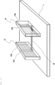
- Fig. 2 is a perspective view showing a first configuration example of the probe 10 according to the embodiment of the invention.
- Fig. 3 is a front view of the first configuration example.
- Fig. 4 is a front view showing an internal configuration of the first configuration example.
- the probe 10 includes a pair of transmission conductors 12 and 14 and a linear conductor 16 connecting signal conductors of the transmission conductors. Dimensions shown in Figs. 2 and 3 are data used in a simulation experiment to be described later.
- the transmission conductors 12 and 14 are coaxial lines, the transmission conductor 12 includes a signal conductor 12a (first signal conductor) which is a core wire and a ground conductor 12b (first ground conductor) which is an outer conductor disposed around (in the vicinity of) the signal conductor 12a via a dielectric layer, and the transmission conductor 14 includes a signal conductor 14a (second signal conductor) which is a core wire and a ground conductor 14b (second ground conductor) which is an outer conductor disposed around (in the vicinity of) the signal conductor 14a via a dielectric layer.
- the transmission conductors 12 and 14 are disposed at a predetermined interval in a width direction.
- Tip ends of the signal conductors 12a and 14a are disposed with a predetermined gap away from a surface of the magnetic body 1 as the sample. Tip ends of the ground conductors 12b and 14b are in contact with the surface of the magnetic body 1 to be evaluated.
- the linear conductor 16 is an elongated strip line extending between the tip ends in a manner of connecting the tip ends of the signal conductors 12a and 14a.
- the linear conductor 16 also extends parallel to the surface of the magnetic body 1 with a predetermined gap length from the surface of the magnetic body 1.
- the linear conductor 16 is formed with a width smaller than that of the ground conductors 12b and 14b forming the outer conductor of the coaxial line so as to prevent spread of a current in the magnetic body 1.
- the ground conductors 12b and 14b around the signal conductors 12a and 14a are processed in a manner of not being in contact with the linear conductor 16.
- the linear conductor 16 may be formed of, for example, a copper wire, a copper foil, or the like.
- the transmission conductors 12 and 14 are connected to the signal cable (for example, coaxial cable) 3 via a connector (not shown) on the other end side, and are connected to the network analyzer 20.
- a current signal supplied from the network analyzer 20 is transmitted through the signal conductors 12a and 14a and the linear conductor 16.
- the transmission conductors 12 and 14 and the linear conductor 16 that constitute the probe 10 are integrally formed using an existing film processing technique such as vapor deposition.
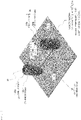
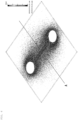
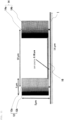
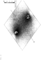
- Figs. 5 and 6 are diagrams showing simulation results of current densities and distributions flowing through the probe 10 and the magnetic body 1.
- Fig. 5 shows a density and distribution of a high frequency current (for example, about 1 GHz) flowing from the signal conductor 12a to the signal conductor 14a via the linear conductor 16.
- Fig. 6 shows a current density and distribution of an eddy current flowing through the magnetic body 1 due to the high frequency current.
- a large current flows in a narrow range along the linear conductor 16, and a result is obtained that the spread of the current in the magnetic body 1 is prevented.
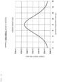
- Fig. 7 is a graph showing a current density on the surface of the magnetic body 1 on a line A (a center line between the transmission conductors) shown in Fig. 6 , and shows a current distribution having a high sharp peak indicating that a large current flows in a thin and narrow range along the linear conductor 16 between the transmission conductors. Accordingly, the spread of the current in the magnetic body 1 is significantly prevented. According to the probe 10 in the invention, the current can be concentrated on a local portion of the magnetic body 1, spread of the current in the magnetic body 1 and reduction of an impedance due to the spread of the current are prevented, and a characteristic impedance is matched to around 50 ⁇ , so that multiple reflections are prevented, a high SN ratio is obtained, and broadband measurement can be performed.
- Fig. 8 is a graph showing a simulation result of a current density when gap lengths between the linear conductor 16 and the magnetic body 1 are different in the first configuration example.
- Fig. 9 is a perspective view showing a second configuration example of the probe 10 according to the embodiment of the invention.
- the transmission conductors 12 and 14 are formed with coplanar lines as compared with the first configuration example.
- the ground conductors 12b and 14b are formed on both sides of the signal conductors 12a and 14a disposed on opposing surfaces of a pair of dielectric substrates.
- the tip ends of the signal conductors 12a and 14a are not in contact with but close to the magnetic body 1.
- the tip ends of the ground conductors 12b and 14b are in contact with the surface of the magnetic body 1 to be evaluated.
- the linear conductor 16 extends between the tip ends of the signal conductors 12a and 14a and connects the tip ends of the signal conductors 12a and 14a.
- the linear conductor 16 has a width equal to or smaller than a width of the signal conductors 12a and 14a so as to prevent the spread of the current in the magnetic body 1.
- the transmission conductors 12 and 14 may be formed with microstrip lines. Also in this case, the linear conductor 16 has the width equal to or smaller than the width of the signal conductors 12a and 14a so as to prevent the spread of the current in the magnetic body 1.
- Fig. 10 is a perspective view showing a third configuration example of the probe 10 according to the embodiment of the invention.
- Fig. 11 is a front view of the third configuration example.
- the probe 10 includes the pair of transmission conductors 12 and 14 and the linear conductor 16 connecting signal conductors of the transmission conductors. Numerical values of dimensions and the like shown in Figs. 10 and 11 are data used in a simulation experiment to be described later.
- the tip ends of the ground conductors 12b and 14b are disposed away from the surface of the magnetic body 1 as the sample by a predetermined gap length, and the tip ends of the signal conductors 12a and 14a are in contact with the surface of the magnetic body 1 to be evaluated.
- the linear conductor 16 is an elongated strip line extending between the tip ends in a manner of connecting the tip ends of the ground conductors 12b and 14b.
- the linear conductor 16 also extends parallel to the surface of the magnetic body 1 and away from the surface of the magnetic body 1 by a predetermined gap length.
- the linear conductor 16 is formed with a width smaller than that of the ground conductors 12b and 14b forming the outer conductor of the coaxial line so as to prevent the spread of the current in the magnetic body 1.
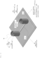
- Figs. 12 and 13 are simulation diagrams showing simulation results of current densities and distributions flowing through the probe 10 and the magnetic body 1.
- Fig. 12 shows the current density and distribution in a plane of the magnetic body 1 of a high frequency current (for example, about 1 GHz) flowing between the signal conductors 12a and 14a in contact with the magnetic body 1.
- Fig. 13 shows the current density and distribution of an eddy current flowing to the linear conductor 16 due to a high frequency current and the ground conductors 12b and 14b.
- a relatively large current flows in the vicinity along the linear conductor 16, and a result is obtained that the spread of the current in the magnetic body 1 is prevented.
- Fig. 14 is a graph showing a current density on the surface of the magnetic body 1 on the line A (the center line between the transmission conductors) shown in Fig. 13 , and shows a current distribution having a high peak indicating that a large current flows in a small and narrow range between the transmission conductors.
- the impedance reduces, and the SN ratio deteriorates due to the reduction of the impedance.
- the probe 10 in the invention since the spread of the current in the magnetic body 1 and the reduction of the impedance due to the spread of the current are prevented, the current can be concentrated on a local portion of the magnetic body 1, and the characteristic impedance is matched to around 50 ⁇ . Therefore, multiple reflections are prevented, a high SN ratio is obtained, and the broadband measurement can be performed.
- Fig. 15 is a perspective view showing a fourth configuration example of the probe 10 according to the embodiment of the invention.
- the transmission conductors 12 and 14 are formed with the microstrip lines as compared with the third configuration example.
- the opposing surfaces of the pair of dielectric substrates are ground conductor surfaces
- the ground conductors 12b and 14b are formed on the ground conductor surfaces
- the signal conductors 12a and 14a are formed on surfaces opposite to the ground conductor surfaces.
- the signal conductors 12a and 14a extend such that the tip ends of the signal conductors 12a and 14a are in contact with the magnetic body 1.
- the tip ends of the ground conductors 12b and 14b are disposed with a predetermined gap away from the surface of the magnetic body 1 as the sample.
- the linear conductor 16 is an elongated strip line extending between the tip ends in a manner of connecting the tip ends of the ground conductors 12b and 14b.
- the linear conductor 16 also extends parallel to the surface of the magnetic body 1 with a predetermined gap length from the surface of the magnetic body 1.
- the linear conductor 16 has a width equal to or smaller than a width of the signal conductors 12a and 14a so as to prevent the spread of the current in the magnetic body 1.
- the transmission conductors 12 and 14 may be formed with coplanar lines. Also in this case, the linear conductor 16 has the width equal to or smaller than the width of the signal conductors 12a and 14a so as to prevent the spread of the current in the magnetic body 1.
- the signal conductors or the ground conductors in the pair of transmission conductors constituting the probe 10 are brought into electrical contact with a magnetic body to be measured, and the remaining ones of the signal conductors and the ground conductors are disposed close to without being in contact with the magnetic body and are electrically connected to each other with a linear conductor. Due to a current flowing through the linear conductor, a current flowing through the sample does not spread in the sample, and a current density in a local portion near the linear conductor significantly protrudes and increases. Accordingly, a local magnetic permeability can be measured with a high SN ratio.
- a film thickness of a manufactured magnetic thin film is as thin as several nm.
- Magnetic permeability of the magnetic thin film is the most basic parameter directly linked to a performance of the magnetic device, and an evaluation of the magnetic permeability of the magnetic thin film in a manufacturing line is extremely important to improve yield of thin-film magnetic devices.
- the probe according to the embodiment of the invention is capable of measuring micron-order local magnetic permeability in a magnetic thin film having an ultrathin film thickness with high accuracy.
- Figs. 16 and 17 are diagrams showing a fifth configuration example of the probe 10 according to the embodiment of the invention, in which Fig. 16 is a perspective view showing an entire configuration of the probe 10, Fig. 17A is a top view, Fig. 17B is a front view, Fig. 17C is a bottom view, and Fig. 17D is a side view.
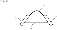
- Fig. 18 is a schematic diagram showing a structure of the probe 10 in the fifth configuration example.
- Fig. 19 is a schematic diagram showing a modification of the structure of the probe 10 in the fifth configuration example.
- the probe 10 includes a microstrip line 17 having a dielectric sandwiched between a microstrip conductor 17a and a ground conductor, and connectors 18 connecting both ends of the microstrip line 17.
- a 50 ⁇ coaxial cable 3 is connected to the connector 18 and is connected to the network analyzer 20.
- the microstrip line 17 is manufactured by etching a printed circuit board made of, for example, fluorine resin (for example, polytetrafluoroethylene (PTFE)).
- fluorine resin for example, polytetrafluoroethylene (PTFE)
- the probe 10 further includes a body 19 that holds the microstrip line 17 and the connectors 18 at predetermined positions.
- the body 19 is formed of a metal such as phosphor bronze or brass, and has a substantially triangular front shape.
- a convex curved portion is formed on a top portion of the body 19, and the microstrip line 17 is curved along the convex curved portion in a manner of straddling the top portion of the body 19.
- the connectors 18 are attached along both inclined surfaces extending downward from the top portion of the body 19.
- the connectors 18 hold the microstrip line 17 disposed in a curved manner at an opening angle of about 90 degrees.
- oblique sides sandwiching the top portion of the body 19 have an opening angle of 90 degrees, and the connectors 18 on both sides are disposed on the body 19 with that angle.
- the probe 10 can be disposed in close proximity without being restricted by a size of the magnetic body, and by forming the microstrip line 17 in a curved shape without a bent portion, deterioration of the characteristic impedance can be minimized, and the broadband measurement can be performed.
- a frequency range up to 40 GHz which is measurable in the related art, can be broadened to a high frequency band up to about 67 GHz.
- the opening angle of the connectors 18 is not limited to the angle of about 90 degrees described above, and can be appropriately determined in an obtuse angle direction within an angle range that falls within a size of the probe 10 that can be disposed between coil intervals of a Helmholtz coil, and in an acute angle direction within an angle range that does not cause impedance mismatch.
- a head portion of the probe 10 is reduced in size, and local magnetic permeability can be measured with a high SN ratio by measuring the magnetic permeability by bringing the probe into direct contact with a local portion of the magnetic body to be evaluated.
- a high SN ratio can be obtained even in a micron-order local portion by a method of directly applying a high frequency current to the magnetic thin film.
- the probe according to the embodiment of the invention can measure micron-order local magnetic permeability in a magnetic thin film having ultrathin film thickness with high accuracy.
- a flat portion 19a is provided at a tip end of the convex curved portion in the top portion of the body 19, and a portion of the microstrip line 17 along the flat portion 19a is linearly disposed.
- an entire length of the microstrip line 17 is about 16 mm
- a width of the flat portion 19a is about 1 mm to 2 mm.
- a thickness of the probe 10 orthogonal to the length of the microstrip line 17 is about 20 mm.
- Shapes of the flat portion and a curved portion are designed in a manner of being continuously connected to each other so as not to form a bent portion (or a step portion or a corner portion).
- Fig. 20 is a diagram showing a measurement result of a characteristic impedance of the probe 10 in the fifth configuration example.
- the characteristic impedance of the probe 10 is measured according to a time domain reflection method (TDR method).
- An end of the probe 10 (an end portion of a connector 16 connected to the coaxial cable 3) is matched with a 50 ⁇ resistance.
- Fig. 21 is a graph of a measurement result of magnetic permeability by a magnetic permeability measuring device using the probe 10 in the fifth configuration example.
- Fig. 22 is a flowchart showing a procedure of a magnetic permeability measuring method according to the embodiment of the invention.
- the transmission coefficient (S 21 ) depending on presence or absence of a permanent magnet for saturating the magnetic body 1 is measured by the network analyzer 20.
- a background is a time when the probe 10 is brought into contact with the magnetic body 1 and the permanent magnet (Helmholtz coil) is disposed in close proximity to saturate the magnetic body 1, and the transmission coefficient at this time is set as a reference signal.
- the transmission coefficient when the permanent magnet is removed is measured.
- the transmission coefficient at this time is a difference signal from the reference signal, that is, a difference value between the transmission coefficients of both presence and absence of the permanent magnet, and this transmission coefficient reflects a magnetic characteristic of the magnetic body 1.
- the difference value between the transmission coefficients is an impedance component due to contribution of the magnetic body 1.
- the impedance, Z is a difference value between the transmission coefficients
- a real part is a loss component (resistance component) R of the magnetic body 1
- an imaginary part is the inductance component L of the magnetic body 1.
- the inductance component L corresponds to the real part ( ⁇ ') of the magnetic permeability of the magnetic body 1
- the resistance component R corresponds to the imaginary part ( ⁇ ") of the magnetic permeability of the magnetic body 1.
- Fig. 23 is a diagram schematically showing a shape of a magnetic thin film as a magnetic body sample to be evaluated.
- the higher a frequency the more current flows only on a surface of the film due to a skin effect.
- ⁇ ' and ⁇ " are repeatedly calculated according to a Newton-Raphson method using, for example, the above equation (2) and following equations (3) and (4) as the numerical analysis processing, and the complex magnetic permeability is obtained by optimization processing such that a predetermined evaluation function value is minimized (S108).
- Equation 4] k 1 + j ⁇ ⁇
- Z is an impedance
- ⁇ is resistivity
- I is a sample length
- w is a sample width
- t is a film thickness
- f is a frequency
- ⁇ is complex magnetic permeability
Landscapes
- Physics & Mathematics (AREA)
- General Physics & Mathematics (AREA)
- Electromagnetism (AREA)
- Condensed Matter Physics & Semiconductors (AREA)
- Measuring Magnetic Variables (AREA)
- Measuring Leads Or Probes (AREA)
Abstract
Description
- The present invention relates to a magnetic permeability measuring probe and a magnetic permeability measuring device using the same
- Many methods of measuring a high frequency magnetic permeability of a magnetic body (usually, several hundred kHz to several GHz) have been proposed since the 1950s, but all of the methods result in a method using a coil (or an antenna) (see, for example, Non-Patent
Literatures 1 to 3) or a method using a transmission line, a waveguide, or the like (see, for example, Non-Patent Literature 4). On the other hand, a method of measuring resistivity by bringing a short needle into contact with a material (for example, see Non-Patent Literature 5) is a widely used method, but this method is to measure the resistivity of the material, and is not to measure magnetic permeability. - The present inventors have published a paper for obtaining magnetic permeability from an impedance of a fine strip thin film having a width of about 100 µm (see, for example, Non-Patent Literature 6).
Patent Literature 1 discloses a measurement method applicable to a magnetic thin film of any size, not limited to a strip.Patent Literature 2 discloses a method capable of evaluating magnetic permeability by disposing a meander-shaped probe close to a magnetic thin film.Patent Literature 3 discloses a method of measuring magnetic permeability by bringing a linear shape portion of a linear microstrip conductor formed of one linear shape portion close to a magnetic body with an insulator sandwiched therebetween. -
- PTL 1:
JP-A-2010-060367 - PTL 2:
JP-A-2012-032165 - PTL 3:
JP-A-2015-172497 -
- Non-Patent Literature 1: P.A.Calcagno, D.A.Thompson, "Semiautomaticpermeance tester for thick magnetic films", Rev. Sci. Instrum, 1975, 46, p.904
- Non-Patent Literature 2: B.C.Webb,M.E.Re, C.V.Jahnes and M.A.Russak, "High-frequency permeability of laminatedand unlaminated, narrow thin-film magnetic stripes", J. Appl. Phys., 1991, vol 69, p.5611-5615
- Non-Patent Literature 3: M.Yamaguchi,S.Yabukami and K.I.Arai, "A New1MHz-2GHz Permeance Meter For Metallic Thin Films", IEEE Trans. Magn., 1997, 33, p.3619
- Non-Patent Literature 4: H.B.Weir, "Automatic Measurement of Complex Dielectric Constant and Permeability atMicrowave Frequencies", Proc IEEE, 1975, 62, p.33
- Non-Patent Literature 5: L.B.Valdes, "Resistivity measurements on germanium for transistors", Proc. IRE, 1954, p.420-427
- Non-Patent Literature 6: S.Yabukami,T.Uo, M.Yamaguchi, K.I.Arai, and M.Takezawa, "High sensitivity permeability measurements of striped films obtained by input impedance", IEEETransactions, Magn., 2001, vol.37, p.2774-2778
- In recent years, a magnetic device using a magnetic thin film has great marketability such as magnetic recording and an MRAM, and a film thickness of the manufactured magnetic thin film is as thin as several nm. Magnetic permeability of the magnetic thin film is the most basic parameter directly related to a performance of the magnetic device, and evaluation of the magnetic permeability of the magnetic thin film in a manufacturing line is also important from the viewpoint of improving yield of a thin film magnetic device.
- As described above, evaluation of a magnetic thin film having a film thickness of about several nm is fairly important, but the film thickness is about 100 nm or more in a magnetic permeability measuring method in the related art above, and it is difficult to evaluate high frequency magnetic permeability of an ultrathin film having a film thickness of several nm. There is a technique for evaluating a high frequency magnetic characteristic such as ferromagnetic resonance, but this technique is a technique for integrally fabricating a transmission line and a magnetic thin film by a microfabrication technique and performing evaluation, and is not a general-purpose evaluation technique.
- There is a need for evaluating a micron-order local magnetic characteristic (measuring magnetic permeability, damping constant, magnetostriction constant, and the like) in a thin film magnetic device represented by an MRAM and the like, and there is a restriction on a size of a probe and the like in a measuring device in the related art, and it is difficult to measure magnetic permeability.
- Therefore, an object of the invention is to provide a magnetic permeability measuring probe and a magnetic permeability measuring device using the same, which can measure local magnetic permeability of a magnetic body such as a magnetic thin film particularly at a high SN ratio.
- A configuration of a magnetic permeability measuring probe in the invention for achieving the above object is a probe configured to measure magnetic permeability of a magnetic body, the probe including: a first signal conductor and a second signal conductor that form a pair of signal conductors, the first signal conductor and the second signal conductor being a signal transmission path transmitting a supplied current signal; a first ground conductor and a second ground conductor that form a pair of ground conductors disposed in the vicinity of the pair of signal conductors; and a linear conductor that electrically connects tip ends of the first signal conductor and the second signal conductor or tip ends of the first ground conductor and the second ground conductor and that extends between the tip ends, in which (i) the tip ends of the first signal conductor and the second signal conductor are disposed away from a surface of the magnetic body by a predetermined gap length and at a predetermined interval from each other, the tip ends of the first ground conductor and the second ground conductor are in contact with the surface of the magnetic body, and the linear conductor electrically connects the tip ends of the first signal conductor and the second signal conductor to each other, or (ii) the tip ends of the first signal conductor and the second signal conductor are in contact with the surface of the magnetic body and are disposed at a predetermined interval from each other, the tip ends of the first ground conductor and the second ground conductor are disposed away from the surface of the magnetic body by a predetermined gap length, and the linear conductor electrically connects the tip ends of the first ground conductor and the second ground conductor to each other.
- As one form example, the first signal conductor and the first ground conductor form a first coaxial line, and the second signal conductor and the second ground conductor form a second coaxial line. When the coaxial line is formed, the linear conductor has a width smaller than diameters of the first coaxial line and the second coaxial line.
- As another form example, the first signal conductor and the first ground conductor form a first coplanar line, and the second signal conductor and the second ground conductor form a second coplanar line. As a further form example, the first signal conductor and the first ground conductor form a first microstrip line, and the second signal conductor and the second ground conductor form a second microstrip line. When the coplanar line or the microstrip line is formed, the linear conductor has a width equal to or smaller than a width of the first signal conductor and the second signal conductor. The linear conductor is in parallel to the surface of the magnetic body and away from the surface of the magnetic body by the gap length.
- Another configuration of the magnetic permeability measuring probe in the invention is a probe configured to measure magnetic permeability of a magnetic body, the probe including: a microstrip line that is a portion in contact with the magnetic body and that is formed by sandwiching a dielectric between a microstrip conductor and a ground conductor; connectors each connected to a respective one of both ends of the microstrip line; and a body that holds the microstrip line and the connectors, in which the body has a convex curved portion on a top portion of the body, and the microstrip line is curved along the convex curved portion straddling the top portion of the body.
- As one form example, a flat portion is provided at a top portion of the convex curved portion of the body, and a portion of the microstrip line along the flat portion is linearly disposed.
- As another form example, the connectors are attached to side surfaces extending downward from the top portion of the body.
- A magnetic permeability measuring device according to the invention includes: the probe having any one of the above configurations; a magnetic field applying portion configured to apply a magnetic field to the magnetic body; a signal measuring instrument that is connected to the probe via a cable and that is configured to measure a signal of a transmission coefficient both presence and absence of magnetic field application by the magnetic field applying portion; and a processing unit configured to obtain, based on the signal of the transmission coefficient measured by the signal measuring instrument, magnetic permeability of the magnetic body by numerical analysis calculation processing.
- According to the magnetic permeability measuring probe and the magnetic permeability measuring device using the same in the invention, deterioration of a characteristic impedance is prevented, and the magnetic permeability can be measured with a high SN ratio and a broad band. In particular, magnetic permeability of a magnetic thin film in a magnetic device such as an MRAM can be evaluated with high accuracy.
-
- [
Fig. 1] Fig. 1 is a diagram showing a schematic configuration example of a magnetic permeability measuring device according to an embodiment of the invention. - [
Fig. 2] Fig. 2 is a perspective view showing a first configuration example of aprobe 10 according to the embodiment of the invention. - [
Fig. 3] Fig. 3 is a front view showing the first configuration example of theprobe 10 according to the embodiment of the invention. - [
Fig. 4] Fig. 4 is a diagram showing an internal configuration of the first configuration example of theprobe 10 according to the embodiment of the invention. - [
Fig. 5] Fig. 5 is a simulation diagram of a current density and distribution flowing through theprobe 10. - [
Fig. 6] Fig. 6 is a simulation diagram of a current density and distribution flowing through amagnetic body 1. - [
Fig. 7] Fig. 7 is a graph showing a current density of a line A shown inFig. 6 . - [
Fig. 8] Fig. 8 is a graph showing a simulation result of a current density when gap lengths between alinear conductor 16 and themagnetic body 1 are different in the first configuration example. - [
Fig. 9] Fig. 9 is a perspective view showing a second configuration example of theprobe 10 according to the embodiment of the invention. - [
Fig. 10] Fig. 10 is a perspective view showing a third configuration example of theprobe 10 according to the embodiment of the invention. - [
Fig. 11] Fig. 11 is a front view showing the third configuration example of theprobe 10 according to the embodiment of the invention. - [
Fig. 12] Fig. 12 is a simulation diagram of current densities and distributions flowing through theprobe 10 and themagnetic body 1. - [
Fig. 13] Fig. 13 is a simulation diagram of a current density and distribution flowing through themagnetic body 1. - [
Fig. 14] Fig. 14 is a graph showing a current density of the line A shown inFig. 13 . - [
Fig. 15] Fig. 15 is a perspective view showing a fourth configuration example of theprobe 10 according to the embodiment of the invention. - [
Fig. 16] Fig. 16 is a diagram showing a fifth configuration example of theprobe 10 according to the embodiment of the invention. - [
Fig. 17] Fig. 17A through Fig. 17D are diagrams showing the fifth configuration example of theprobe 10 according to the embodiment of the invention. - [
Fig. 18] Fig. 18 is a schematic diagram showing a structure of theprobe 10 in the fifth configuration example. - [
Fig. 19] Fig. 19 is a schematic diagram showing a modification of the structure of theprobe 10 in the fifth configuration example. - [
Fig. 20] Fig. 20 is a diagram showing a measurement result of a characteristic impedance of theprobe 10 in the fifth configuration example. - [
Fig. 21] Fig. 21 is a graph of a measurement result of magnetic permeability by a magnetic permeability measuring device using theprobe 10 in the fifth configuration example. - [
Fig. 22] Fig. 22 is a flowchart showing a procedure of a magnetic permeability measuring method according to the embodiment of the invention. - [
Fig. 23] Fig. 23 is a diagram schematically showing a shape of a magnetic thin film as a magnetic body sample to be evaluated. - Hereinafter, an embodiment of the invention will be described with reference to the drawings. However, such an example of the embodiment does not limit the technical scope of the invention.
-
Fig. 1 is a diagram showing a schematic configuration example of a magnetic permeability measuring device according to an embodiment of the invention. A magnetic permeability measuring device according to the embodiment of the invention includes aprobe 10, a network analyzer 20 (signal measuring instrument), and a calculation processing device (for example, a computer device such as a personal computer) 30 (processing unit) that executes numerical analysis processing. - The
probe 10 is disposed in contact with or in proximity to amagnetic body 1 as a sample, and is connected to thenetwork analyzer 20 via asignal cable 3. Thenetwork analyzer 20 is a current supply source capable of supplying a current signal, and measures the transmission coefficient (S21) of themagnetic body 1 to be evaluated by thenetwork analyzer 20, takes signal data thereof into the controlpersonal computer 30, and obtains complex magnetic permeability of a magnetic body by predetermined numerical analysis processing (for example, optimization processing). In order to magnetically saturate themagnetic body 1, a magnet (magnetic field applying portion) formed of a Helmholtz coil (electromagnetic coil) is used. -
Fig. 2 is a perspective view showing a first configuration example of theprobe 10 according to the embodiment of the invention.Fig. 3 is a front view of the first configuration example.Fig. 4 is a front view showing an internal configuration of the first configuration example. Theprobe 10 includes a pair oftransmission conductors linear conductor 16 connecting signal conductors of the transmission conductors. Dimensions shown inFigs. 2 and3 are data used in a simulation experiment to be described later. - The
transmission conductors transmission conductor 12 includes asignal conductor 12a (first signal conductor) which is a core wire and aground conductor 12b (first ground conductor) which is an outer conductor disposed around (in the vicinity of) thesignal conductor 12a via a dielectric layer, and thetransmission conductor 14 includes asignal conductor 14a (second signal conductor) which is a core wire and aground conductor 14b (second ground conductor) which is an outer conductor disposed around (in the vicinity of) thesignal conductor 14a via a dielectric layer. Thetransmission conductors signal conductors magnetic body 1 as the sample. Tip ends of theground conductors magnetic body 1 to be evaluated. - The
linear conductor 16 is an elongated strip line extending between the tip ends in a manner of connecting the tip ends of thesignal conductors linear conductor 16 also extends parallel to the surface of themagnetic body 1 with a predetermined gap length from the surface of themagnetic body 1. Thelinear conductor 16 is formed with a width smaller than that of theground conductors magnetic body 1. As shown, in order to connect the tip ends of thesignal conductors ground conductors signal conductors linear conductor 16. Thelinear conductor 16 may be formed of, for example, a copper wire, a copper foil, or the like. - The
transmission conductors network analyzer 20. A current signal supplied from thenetwork analyzer 20 is transmitted through thesignal conductors linear conductor 16. Thetransmission conductors linear conductor 16 that constitute theprobe 10 are integrally formed using an existing film processing technique such as vapor deposition. -
Figs. 5 and6 are diagrams showing simulation results of current densities and distributions flowing through theprobe 10 and themagnetic body 1.Fig. 5 shows a density and distribution of a high frequency current (for example, about 1 GHz) flowing from thesignal conductor 12a to thesignal conductor 14a via thelinear conductor 16.Fig. 6 shows a current density and distribution of an eddy current flowing through themagnetic body 1 due to the high frequency current. In themagnetic body 1 as the sample, a large current flows in a narrow range along thelinear conductor 16, and a result is obtained that the spread of the current in themagnetic body 1 is prevented. This is because the high frequency current flowing in themagnetic body 1 as the sample is collected directly below thelinear conductor 16, so that a difference between a current distribution and an impedance at the time of calibration by applying a strong magnetic field is increased, and an SN ratio when magnetic permeability is acquired is improved. -
Fig. 7 is a graph showing a current density on the surface of themagnetic body 1 on a line A (a center line between the transmission conductors) shown inFig. 6 , and shows a current distribution having a high sharp peak indicating that a large current flows in a thin and narrow range along thelinear conductor 16 between the transmission conductors. Accordingly, the spread of the current in themagnetic body 1 is significantly prevented. According to theprobe 10 in the invention, the current can be concentrated on a local portion of themagnetic body 1, spread of the current in themagnetic body 1 and reduction of an impedance due to the spread of the current are prevented, and a characteristic impedance is matched to around 50 Ω, so that multiple reflections are prevented, a high SN ratio is obtained, and broadband measurement can be performed. -
Fig. 8 is a graph showing a simulation result of a current density when gap lengths between thelinear conductor 16 and themagnetic body 1 are different in the first configuration example. The narrower the gap length between thelinear conductor 16 and themagnetic body 1, the higher an effect of increasing a current density in a region where thelinear conductor 16 extends. Even with a slightly widened configuration, the current can be collected in a narrow range along thelinear conductor 16, and the spread of the current in themagnetic body 1 is effectively prevented. -
Fig. 9 is a perspective view showing a second configuration example of theprobe 10 according to the embodiment of the invention. In the second configuration example, thetransmission conductors transmission conductors ground conductors signal conductors signal conductors magnetic body 1. The tip ends of theground conductors magnetic body 1 to be evaluated. Thelinear conductor 16 extends between the tip ends of thesignal conductors signal conductors linear conductor 16 has a width equal to or smaller than a width of thesignal conductors magnetic body 1. - Although not shown, in the first configuration example or the second configuration example, the
transmission conductors linear conductor 16 has the width equal to or smaller than the width of thesignal conductors magnetic body 1. -
Fig. 10 is a perspective view showing a third configuration example of theprobe 10 according to the embodiment of the invention.Fig. 11 is a front view of the third configuration example. Similarly to the first configuration example and the second configuration example, theprobe 10 includes the pair oftransmission conductors linear conductor 16 connecting signal conductors of the transmission conductors. Numerical values of dimensions and the like shown inFigs. 10 and11 are data used in a simulation experiment to be described later. - In the third configuration example, as compared with the first configuration example, in the
transmission conductors ground conductors magnetic body 1 as the sample by a predetermined gap length, and the tip ends of thesignal conductors magnetic body 1 to be evaluated. Thelinear conductor 16 is an elongated strip line extending between the tip ends in a manner of connecting the tip ends of theground conductors linear conductor 16 also extends parallel to the surface of themagnetic body 1 and away from the surface of themagnetic body 1 by a predetermined gap length. Thelinear conductor 16 is formed with a width smaller than that of theground conductors magnetic body 1. -
Figs. 12 and13 are simulation diagrams showing simulation results of current densities and distributions flowing through theprobe 10 and themagnetic body 1.Fig. 12 shows the current density and distribution in a plane of themagnetic body 1 of a high frequency current (for example, about 1 GHz) flowing between thesignal conductors magnetic body 1.Fig. 13 shows the current density and distribution of an eddy current flowing to thelinear conductor 16 due to a high frequency current and theground conductors magnetic body 1, a relatively large current flows in the vicinity along thelinear conductor 16, and a result is obtained that the spread of the current in themagnetic body 1 is prevented. -
Fig. 14 is a graph showing a current density on the surface of themagnetic body 1 on the line A (the center line between the transmission conductors) shown inFig. 13 , and shows a current distribution having a high peak indicating that a large current flows in a small and narrow range between the transmission conductors. When the current spreads in the plane of themagnetic body 1, the impedance reduces, and the SN ratio deteriorates due to the reduction of the impedance. However, according to theprobe 10 in the invention, since the spread of the current in themagnetic body 1 and the reduction of the impedance due to the spread of the current are prevented, the current can be concentrated on a local portion of themagnetic body 1, and the characteristic impedance is matched to around 50 Ω. Therefore, multiple reflections are prevented, a high SN ratio is obtained, and the broadband measurement can be performed. -
Fig. 15 is a perspective view showing a fourth configuration example of theprobe 10 according to the embodiment of the invention. In the fourth configuration example, thetransmission conductors - In the
transmission conductors ground conductors signal conductors signal conductors signal conductors magnetic body 1. The tip ends of theground conductors magnetic body 1 as the sample. Thelinear conductor 16 is an elongated strip line extending between the tip ends in a manner of connecting the tip ends of theground conductors linear conductor 16 also extends parallel to the surface of themagnetic body 1 with a predetermined gap length from the surface of themagnetic body 1. Thelinear conductor 16 has a width equal to or smaller than a width of thesignal conductors magnetic body 1. - Although not shown, in the third configuration example or the fourth configuration example, the
transmission conductors linear conductor 16 has the width equal to or smaller than the width of thesignal conductors magnetic body 1. - The signal conductors or the ground conductors in the pair of transmission conductors constituting the
probe 10 are brought into electrical contact with a magnetic body to be measured, and the remaining ones of the signal conductors and the ground conductors are disposed close to without being in contact with the magnetic body and are electrically connected to each other with a linear conductor. Due to a current flowing through the linear conductor, a current flowing through the sample does not spread in the sample, and a current density in a local portion near the linear conductor significantly protrudes and increases. Accordingly, a local magnetic permeability can be measured with a high SN ratio. - For example, in a magnetic device such as a magnetoresistive random access memory (MRAM), a film thickness of a manufactured magnetic thin film is as thin as several nm. Magnetic permeability of the magnetic thin film is the most basic parameter directly linked to a performance of the magnetic device, and an evaluation of the magnetic permeability of the magnetic thin film in a manufacturing line is extremely important to improve yield of thin-film magnetic devices. The probe according to the embodiment of the invention is capable of measuring micron-order local magnetic permeability in a magnetic thin film having an ultrathin film thickness with high accuracy.
-
Figs. 16 and17 are diagrams showing a fifth configuration example of theprobe 10 according to the embodiment of the invention, in whichFig. 16 is a perspective view showing an entire configuration of theprobe 10,Fig. 17A is a top view,Fig. 17B is a front view,Fig. 17C is a bottom view, andFig. 17D is a side view.Fig. 18 is a schematic diagram showing a structure of theprobe 10 in the fifth configuration example.Fig. 19 is a schematic diagram showing a modification of the structure of theprobe 10 in the fifth configuration example. - The
probe 10 includes amicrostrip line 17 having a dielectric sandwiched between amicrostrip conductor 17a and a ground conductor, andconnectors 18 connecting both ends of themicrostrip line 17. A 50 Ωcoaxial cable 3 is connected to theconnector 18 and is connected to thenetwork analyzer 20. Themicrostrip line 17 is manufactured by etching a printed circuit board made of, for example, fluorine resin (for example, polytetrafluoroethylene (PTFE)). - The
probe 10 further includes abody 19 that holds themicrostrip line 17 and theconnectors 18 at predetermined positions. Thebody 19 is formed of a metal such as phosphor bronze or brass, and has a substantially triangular front shape. A convex curved portion is formed on a top portion of thebody 19, and themicrostrip line 17 is curved along the convex curved portion in a manner of straddling the top portion of thebody 19. Theconnectors 18 are attached along both inclined surfaces extending downward from the top portion of thebody 19. Preferably, theconnectors 18 hold themicrostrip line 17 disposed in a curved manner at an opening angle of about 90 degrees. Therefore, oblique sides sandwiching the top portion of thebody 19 have an opening angle of 90 degrees, and theconnectors 18 on both sides are disposed on thebody 19 with that angle. By setting the opening angle of twoconnectors 18 to about 90 degrees, theprobe 10 can be disposed in close proximity without being restricted by a size of the magnetic body, and by forming themicrostrip line 17 in a curved shape without a bent portion, deterioration of the characteristic impedance can be minimized, and the broadband measurement can be performed. In the probe according to the present embodiment, a frequency range up to 40 GHz, which is measurable in the related art, can be broadened to a high frequency band up to about 67 GHz. - The opening angle of the
connectors 18 is not limited to the angle of about 90 degrees described above, and can be appropriately determined in an obtuse angle direction within an angle range that falls within a size of theprobe 10 that can be disposed between coil intervals of a Helmholtz coil, and in an acute angle direction within an angle range that does not cause impedance mismatch. - A head portion of the
probe 10 is reduced in size, and local magnetic permeability can be measured with a high SN ratio by measuring the magnetic permeability by bringing the probe into direct contact with a local portion of the magnetic body to be evaluated. In particular, in the present probe having the ground conductor, a high SN ratio can be obtained even in a micron-order local portion by a method of directly applying a high frequency current to the magnetic thin film. - As described above, for a thin film magnetic device such as a magnetoresistive random access memory (MRAM), the probe according to the embodiment of the invention can measure micron-order local magnetic permeability in a magnetic thin film having ultrathin film thickness with high accuracy.
- As the modification of the structure of the
probe 10 in the fifth configuration example, as shown inFig. 19 , a flat portion 19a is provided at a tip end of the convex curved portion in the top portion of thebody 19, and a portion of themicrostrip line 17 along the flat portion 19a is linearly disposed. For example, an entire length of themicrostrip line 17 is about 16 mm, and a width of the flat portion 19a is about 1 mm to 2 mm. A thickness of theprobe 10 orthogonal to the length of themicrostrip line 17 is about 20 mm. Shapes of the flat portion and a curved portion are designed in a manner of being continuously connected to each other so as not to form a bent portion (or a step portion or a corner portion). By providing the flat portion, it is possible to reliably and easily bring theprobe 10 into contact with a desired position of the magnetic body at the time of measurement, and it is possible to perform measurement efficiently. -
Fig. 20 is a diagram showing a measurement result of a characteristic impedance of theprobe 10 in the fifth configuration example. The characteristic impedance of theprobe 10 is measured according to a time domain reflection method (TDR method). An end of the probe 10 (an end portion of aconnector 16 connected to the coaxial cable 3) is matched with a 50 Ω resistance. -
Fig. 21 is a graph of a measurement result of magnetic permeability by a magnetic permeability measuring device using theprobe 10 in the fifth configuration example. A sample to be evaluated is a Ni-Ferrite thin film (8 mm × 5 mm × 1.2 µm in thickness), and a result was obtained in which complex magnetic permeability (µ = µ' - jµ") up to a high frequency band of about 67 Ghz can be measured at a high SN ratio. - A measurement procedure by the magnetic permeability measuring device provided with each
probe 10 in the above-mentioned first to fifth configuration examples will be described below. -
Fig. 22 is a flowchart showing a procedure of a magnetic permeability measuring method according to the embodiment of the invention. Themicrostrip line 14 of theprobe 10 is brought into contact with themagnetic body 1 to be evaluated (S100). Then, themagnetic body 1 is placed in a Helmholtz coil, a strong DC magnetic field (for example, about 20 kOe) is applied to saturate themagnetic body 1, and calibration is performed by the network analyzer 20 (S102). Accordingly, electrical lengths of theprobe 10 and thecoaxial cable 3, a DC impedance of the magnetic body, a non-magnetic signal, and the like are removed. Thereafter, the DC magnetic field is released, and a transmission coefficient (S21) of contribution of themagnetic body 1 is measured (S104). The transmission coefficient (S21) is converted into an impedance, Z, of themagnetic body 1 according to a following equation (1) (S106).
[Equation 1]
- Specifically, the transmission coefficient (S21) depending on presence or absence of a permanent magnet for saturating the
magnetic body 1 is measured by thenetwork analyzer 20. A background is a time when theprobe 10 is brought into contact with themagnetic body 1 and the permanent magnet (Helmholtz coil) is disposed in close proximity to saturate themagnetic body 1, and the transmission coefficient at this time is set as a reference signal. Next, the transmission coefficient when the permanent magnet is removed is measured. The transmission coefficient at this time is a difference signal from the reference signal, that is, a difference value between the transmission coefficients of both presence and absence of the permanent magnet, and this transmission coefficient reflects a magnetic characteristic of themagnetic body 1. The difference value between the transmission coefficients is an impedance component due to contribution of themagnetic body 1. - According to the equation (1), the impedance, Z, is a difference value between the transmission coefficients, a real part is a loss component (resistance component) R of the
magnetic body 1, and an imaginary part is the inductance component L of themagnetic body 1. The inductance component L corresponds to the real part (µ') of the magnetic permeability of themagnetic body 1, and the resistance component R corresponds to the imaginary part (µ") of the magnetic permeability of themagnetic body 1. The magnetic permeability (complex magnetic permeability) µ of themagnetic body 1 is expressed according to a following equation (2).
[Equation 2]
-
Fig. 23 is a diagram schematically showing a shape of a magnetic thin film as a magnetic body sample to be evaluated. The higher a frequency, the more current flows only on a surface of the film due to a skin effect. Assuming that the impedance, Z, is determined by biasing the current in a film thickness direction due to the skin effect as shown inFig. 23 , µ' and µ" are repeatedly calculated according to a Newton-Raphson method using, for example, the above equation (2) and following equations (3) and (4) as the numerical analysis processing, and the complex magnetic permeability is obtained by optimization processing such that a predetermined evaluation function value is minimized (S108).
[Equation 3]
[Equation 4]
- Z is an impedance, ρ is resistivity, I is a sample length, w is a sample width, t is a film thickness, f is a frequency, and µ is complex magnetic permeability.
- The invention is not limited to the above embodiment, and it is needless to say that design changes that do not depart from the scope of the invention including various modifications and corrections that can be conceived by a person having ordinary knowledge in the field of the invention are included in the invention.
-
- 1 magnetic body (magnetic thin film)
- 3 coaxial cable
- 10 probe
- 12 transmission conductor
- 12a signal conductor
- 12b ground conductor
- 14 transmission conductor
- 14a signal conductor
- 14b ground conductor
- 16 linear conductor
- 17 microstrip line
- 17a microstrip conductor
- 18 connector
- 19 body
- 19a flat portion
- 20 network analyzer (signal measuring instrument)
- 30 calculation processing device
Claims (12)
- A probe configured to measure magnetic permeability of a magnetic body, the probe comprising:a first signal conductor and a second signal conductor that form a pair of signal conductors, the first signal conductor and the second signal conductor being a signal transmission path transmitting a supplied current signal;a first ground conductor and a second ground conductor that form a pair of ground conductors disposed in the vicinity of the pair of signal conductors; anda linear conductor that electrically connects tip ends of the first signal conductor and the second signal conductor or tip ends of the first ground conductor and the second ground conductor and that extends between the tip ends, wherein(i) the tip ends of the first signal conductor and the second signal conductor are disposed away from a surface of the magnetic body by a predetermined gap length and at a predetermined interval from each other, the tip ends of the first ground conductor and the second ground conductor are in contact with the surface of the magnetic body, and the linear conductor electrically connects the tip ends of the first signal conductor and the second signal conductor to each other, or(ii) the tip ends of the first signal conductor and the second signal conductor are in contact with the surface of the magnetic body and are disposed at a predetermined interval from each other, the tip ends of the first ground conductor and the second ground conductor are disposed away from the surface of the magnetic body by a predetermined gap length, and the linear conductor electrically connects the tip ends of the first ground conductor and the second ground conductor to each other.
- The probe according to claim 1, wherein
the first signal conductor and the first ground conductor form a first coaxial line, and the second signal conductor and the second ground conductor form a second coaxial line. - The probe according to claim 1, wherein
the first signal conductor and the first ground conductor form a first coplanar line, and the second signal conductor and the second ground conductor form a second coplanar line. - The probe according to claim 1, wherein
the first signal conductor and the first ground conductor form a first microstrip line, and the second signal conductor and the second ground conductor form a second microstrip line. - The probe according to claim 2, wherein
the linear conductor has a width smaller than diameters of the first coaxial line and the second coaxial line. - The probe according to claim 3 or 4, wherein
the linear conductor has a width equal to or smaller than a width of the first signal conductor and the second signal conductor. - The probe according to any one of claims 1 to 6, wherein
the linear conductor is in parallel with the surface of the magnetic body and away from the surface of the magnetic body by the predetermined gap length. - A probe configured to measure magnetic permeability of a magnetic body, the probe comprising:a microstrip line that is a portion in contact with the magnetic body and that is formed by sandwiching a dielectric between a microstrip conductor and a ground conductor;connectors each connected to a respective one of both ends of the microstrip line; anda body that holds the microstrip line and the connectors, whereinthe body has a convex curved portion on a top portion of the body, and the microstrip line is curved along the convex curved portion straddling the top portion of the body.
- The probe according to claim 8, wherein
a flat portion is provided at a top portion of the convex curved portion of the body, and a portion of the microstrip line along the flat portion is linearly disposed. - The probe according to claim 8 or 9, wherein
the connectors are attached to side surfaces extending downward from the top portion of the body. - The probe according to any one of claims 1 to 10, wherein
the magnetic body is a magnetic thin film. - A magnetic permeability measuring device comprising:the probe according to any one of claims 1 to 11;a magnetic field applying portion configured to apply a magnetic field to the magnetic body;a signal measuring instrument that is connected to the probe via a cable and that is configured to measure a signal of a transmission coefficient both presence and absence of magnetic field application by the magnetic field applying portion; anda processing unit configured to obtain, based on the signal of the transmission coefficient measured by the signal measuring instrument, magnetic permeability of the magnetic body by numerical analysis calculation processing.
Applications Claiming Priority (3)
| Application Number | Priority Date | Filing Date | Title |
|---|---|---|---|
| JP2020061006A JP7489011B2 (en) | 2020-03-30 | 2020-03-30 | Magnetic permeability measuring probe and magnetic permeability measuring device using the same |
| JP2020062596A JP7448898B2 (en) | 2020-03-31 | 2020-03-31 | Magnetic permeability measurement probe and magnetic permeability measurement device using the same |
| PCT/JP2021/012493 WO2021200533A1 (en) | 2020-03-30 | 2021-03-25 | Permeability measuring probe and permeability measuring device |
Publications (2)
| Publication Number | Publication Date |
|---|---|
| EP4130773A1 true EP4130773A1 (en) | 2023-02-08 |
| EP4130773A4 EP4130773A4 (en) | 2023-09-13 |
Family
ID=77929859
Family Applications (1)
| Application Number | Title | Priority Date | Filing Date |
|---|---|---|---|
| EP21780006.9A Pending EP4130773A4 (en) | 2020-03-30 | 2021-03-25 | PERMEABILITY MEASUREMENT PROBE AND PERMEABILITY MEASUREMENT DEVICE |
Country Status (3)
| Country | Link |
|---|---|
| US (1) | US12163990B2 (en) |
| EP (1) | EP4130773A4 (en) |
| WO (1) | WO2021200533A1 (en) |
Families Citing this family (1)
| Publication number | Priority date | Publication date | Assignee | Title |
|---|---|---|---|---|
| WO2025197946A1 (en) * | 2024-03-22 | 2025-09-25 | 国立大学法人東北大学 | Permeability measuring device and permeability measuring method |
Family Cites Families (10)
| Publication number | Priority date | Publication date | Assignee | Title |
|---|---|---|---|---|
| JP2001324522A (en) * | 2000-05-15 | 2001-11-22 | Yuki Shimada | How to measure dielectric constant or magnetic permeability |
| JP4219634B2 (en) * | 2002-08-01 | 2009-02-04 | 凌和電子株式会社 | Magnetic sensor, side-open TEM cell, and apparatus using them |
| JP2006170732A (en) * | 2004-12-15 | 2006-06-29 | Nec Engineering Ltd | Magnetic field sensor |
| JP5151032B2 (en) | 2006-01-13 | 2013-02-27 | 株式会社日立製作所 | Magnetic field probe device and magnetic field probe element |
| KR100877941B1 (en) * | 2007-05-28 | 2009-01-12 | 서울시립대학교 산학협력단 | Probe manufacturing method, probe and measuring device for measuring complex permittivity and complex permeability |
| JP2010060367A (en) * | 2008-09-02 | 2010-03-18 | Tohoku Techno Arch Co Ltd | Permeability measurement device of magnetic substance and permeability measurement method of magnetic substance |
| JP2012032165A (en) * | 2010-07-28 | 2012-02-16 | Makoto Yabugami | Apparatus and method for measuring permeability of magnetic substance |
| JP6362249B2 (en) * | 2014-03-11 | 2018-07-25 | 学校法人東北学院 | Magnetic body permeability measuring device and magnetic body permeability measuring method |
| JP2016053569A (en) * | 2014-09-01 | 2016-04-14 | 学校法人東北学院 | Device and method for measuring magnetic material |
| US10401464B2 (en) * | 2017-03-20 | 2019-09-03 | Taiwan Semiconductor Manufacturing Company, Ltd. | Scanning ferromagnetic resonance (FMR) for wafer-level characterization of magnetic films and multilayers |
-
2021
- 2021-03-25 EP EP21780006.9A patent/EP4130773A4/en active Pending
- 2021-03-25 WO PCT/JP2021/012493 patent/WO2021200533A1/en not_active Ceased
-
2022
- 2022-09-29 US US17/955,732 patent/US12163990B2/en active Active
Also Published As
| Publication number | Publication date |
|---|---|
| US12163990B2 (en) | 2024-12-10 |
| EP4130773A4 (en) | 2023-09-13 |
| US20230025196A1 (en) | 2023-01-26 |
| WO2021200533A1 (en) | 2021-10-07 |
Similar Documents
| Publication | Publication Date | Title |
|---|---|---|
| US12474299B2 (en) | Measurement device and measurement method for measuring permeability and permittivity | |
| JP6362249B2 (en) | Magnetic body permeability measuring device and magnetic body permeability measuring method | |
| US8577632B2 (en) | System and method for identification of complex permittivity of transmission line dielectric | |
| CN106018973B (en) | A kind of micro-strip test nano thin-film Micro-wave low-noise transistor device | |
| Fenner et al. | A comprehensive analysis of free‐space and guided‐wave techniques for extracting the permeability and permittivity of materials using reflection‐only measurements | |
| JP2016053569A (en) | Device and method for measuring magnetic material | |
| JP2010060367A (en) | Permeability measurement device of magnetic substance and permeability measurement method of magnetic substance | |
| JP2012032165A (en) | Apparatus and method for measuring permeability of magnetic substance | |
| CN101819262A (en) | Frequency-conversion ferromagnetic resonance measuring system | |
| CN104297567A (en) | Fixture for measuring antenna impedance on UHF RFID tags | |
| Yabukami et al. | Impact of complex permeability measurements up to millimeter-wave frequency range | |
| US12163990B2 (en) | Permeability measuring probe and permeability measuring device | |
| JP7489011B2 (en) | Magnetic permeability measuring probe and magnetic permeability measuring device using the same | |
| Yabukami et al. | Simultaneous evaluation of permeability and permittivity using a flexible microstrip line-type probe up to 67 GHz | |
| CN205786867U (en) | A kind of nano thin-film Micro-wave low-noise transistor test device | |
| Fernandez et al. | High-frequency magnetoimpedance response of thin-film microstructures using coplanar waveguides | |
| JP7448898B2 (en) | Magnetic permeability measurement probe and magnetic permeability measurement device using the same | |
| TWI759018B (en) | Electromagnetic property measuring device, electromagnetic property measuring system and electromagnetic property measuring method | |
| Rozanov et al. | Microwave measurements of the magnetic film permeability | |
| US7482814B2 (en) | Electric/magnetic field sensor | |
| US5744972A (en) | Device and method to measure the complex permeability of thin films at ultra-high frequencies | |
| JP7752896B2 (en) | Magnetic permeability measurement probe and magnetic permeability measurement device using the same | |
| Azeez et al. | Establishing a new form of primary impedance standard at millimeter-wave frequencies | |
| WO2025027747A1 (en) | Magnetic permeability measuring method | |
| WO2025197946A1 (en) | Permeability measuring device and permeability measuring method |
Legal Events
| Date | Code | Title | Description |
|---|---|---|---|
| STAA | Information on the status of an ep patent application or granted ep patent |
Free format text: STATUS: THE INTERNATIONAL PUBLICATION HAS BEEN MADE |
|
| PUAI | Public reference made under article 153(3) epc to a published international application that has entered the european phase |
Free format text: ORIGINAL CODE: 0009012 |
|
| STAA | Information on the status of an ep patent application or granted ep patent |
Free format text: STATUS: REQUEST FOR EXAMINATION WAS MADE |
|
| 17P | Request for examination filed |
Effective date: 20220914 |
|
| AK | Designated contracting states |
Kind code of ref document: A1 Designated state(s): AL AT BE BG CH CY CZ DE DK EE ES FI FR GB GR HR HU IE IS IT LI LT LU LV MC MK MT NL NO PL PT RO RS SE SI SK SM TR |
|
| DAV | Request for validation of the european patent (deleted) | ||
| DAX | Request for extension of the european patent (deleted) | ||
| A4 | Supplementary search report drawn up and despatched |
Effective date: 20230811 |
|
| RIC1 | Information provided on ipc code assigned before grant |
Ipc: G01N 27/72 20060101ALI20230807BHEP Ipc: G01R 33/12 20060101AFI20230807BHEP |